

Features/Applications
CML Semiconductor Products
PRODUCT INFORMATION
Low-Noise Digitally Controlled
FX009A
Amplifier Array
Publication D/009A/3 July 1994
8 Digitally Controlled Low-Noise
Amplifiers
15 Gain/Attenuation Steps
7 Trimmers, with a ± 3dB Range in
0.43dB Steps
1 'Volume' Trimmer, with a ± 14dB
Range in 2.0dB Steps
SERIAL CLOCK INPUT
SERIAL DATA INPUT
V
DD
V
BIAS
Ch1
Ch2
Ch3
1
2
3
16
12345678
16-LINE STEP CONTROLS TO AMPLIFIERS 1 to 8
OUTPUT MUTE - POWERSAVE*
V
BIAS
*
V
BIAS
*
8 - BIT
SERIAL DATA INPUT
AND
LINE DECODERS
8-Bit Serial Data Control
Output Mute/Powersave Function
Audio and Data Gain Control
Applications
Cellular, PMR, PABX Applications
LOAD/LATCH
LOAD/LATCH
V
5
*
V
BIAS
*
6
SS
Ch5
Ch6
FX009A
V
BIAS
*
7
Ch7
V
4
Ch4
BIAS
*
V
BIAS
4321 56 7
CONTROLLED AUDIO OUTPUT LINES
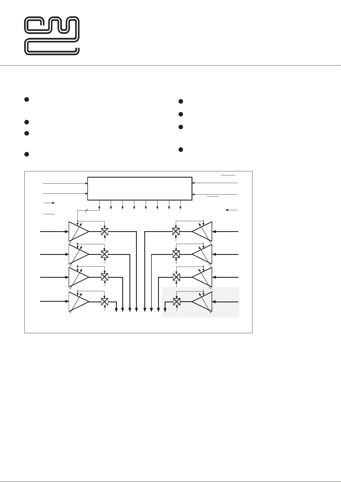
Fig.1 Functional Block Diagram
Brief Description
The FX009A Digitally Adjustable Amplifier Array is
intended to replace trimmer potentiometers and volume
controls in Cellular, PMR, Telephony and
Communications applications where d.c., voice or data
signals need adjustment.
The FX009A is a low-noise single-chip LSI consisting
eight digitally controlled amplifier stages, each with 15
distinct gain/attenuation steps. Control of each
individual amplifier is by an 8-bit serial data stream.
Seven of the amplifier stages offer a +/-3dB range in
steps of 0.43dB, whilst the remaining amplifier offers a
+/-14dB range in steps of 2dB, and is intended for
volume control applications. Each amplifier includes a
16th 'Mute' state which sets the output to bias (VDD/2)
and powersaves the entire section. Minimum current
drain may be achieved by muting all eight sections.
V
BIAS
*
V
8 - VOLUME
BIAS
8
Ch8
This product replaces the need for manual trimming of
audible signals by using the host microprocessor to
digitally control the set-up of all audio levels.
Applications include:
(i) Control, adjustment and set-up of communications
equipment by an Intelligent ATE without manual
intervention – eg. Deviation, Microphone and L/S
Level, Rx Audio Level etc.
(ii) Automatic Dynamic Compensation of drift caused
by variations in temperature, linearity, etc.
(iii)Fully automated servicing and re-alignment.
The FX009A is a low-power, single 5-volt CMOS
device available in both 24-pin DIL and SMD package
versions.
1

Pin Number Function
FX009A
J
FX009A
LG/LS
1
1
Serial Clock : This external clock pulse input is used to “clock in” the Control Data.
See Figure 4, Data Load Timing. This input has an internal 1MΩ pullup resistor.
2
2
Load/Latch : Governs the loading and execution of the control data. During serial
data loading this input should be kept at a logical '0' to ensure that data rippling past
the latches has no effect. When all 8 bits have been loaded, this input should be
strobed '0' ⇒ '1' ⇒ '0' to latch the new data in. Data is executed on the falling edge
of the strobe. If the Load/Latch input is used this pin should be left open circuit. This
input has an internal 1MΩ pullup resistor.
3
3
Load/Latch : The inverted Load/Latch input. This function governs the loading and
execution of the control data. During serial data loading this input should be kept at a
logical '1' to ensure that data rippling past the latches has no effect. When all 8 bits
have been loaded, this input should be strobed '1' - '0' - '1' to latch the new data in.
Data is executed on the rising edge of the strobe. If the Load/Latch input is used this
pin should be left open circuit. This input has an internal 1MΩ pulldown resistor.
4
4
Ch1 Input :
Analogue Inputs :
These individual amplifier inputs are self-biasing, a.c. input
5
5
Ch2 Input :
analogue signals must be capacitively coupled to these pins,
as shown in Figure 2.
6
7
8
6
7
8
Ch3 Input :
Ch4 Input :
V
: The output of the on-chip bias circuitry, held at VDD/2. This pin should be
BIAS
decoupled to VSS as shown in Figure 2.
In the powersave modes the inputs are biased at VDD/2.
Note that amplifiers Ch1 to Ch8 are 'inverting amplifiers.'
9
10
11
12
13
14
15
16
17
18
19
20
21
22
9
10
11
12
13
14
15
16
17
18
19
20
21
22
Ch5 Input :
Analogue Inputs :
Ch6 Input :
Ch7 Input :
Ch8 Input :
VSS : Negative supply rail (GND).
Ch8 Output :
Ch7 Output :
Analogue Outputs :
The individual "Gain Controlled" amplifier outputs.
Ch1 to Ch7 range from -3dB to +3dB in 0.43dB steps, Ch8
Ch6 Output :
could be utilized as a volume control, ranging from -14dB to
+14dB in 2.0dB steps.
Ch5 Output :
In the powersave mode the selected output is biased at VDD/2.
No internal connection. Do not use.
Ch4 Output :
Ch3 Output :
Analogue Outputs
Note that amplifiers Ch1 to Ch8 are 'inverting amplifiers.'
Ch2 Output :
Ch1 Output :
23
24
23
24
VDD : Positive supply rail. A single +5-volt power supply is required.
Control Data Input : Operation of the 8 amplifier channels (Ch1 – Ch8) is controlled
by the 8 bits of data entered serially at this pin . The data is entered (bit 7 to bit 0) on
the rising edge of the external Serial Clock. The data format is described in Tables 1,
2 and Figure 4. This input has an internal 1MΩ pullup resistor.
2

Application Notes
C
V
SS
SERIAL CLOCK INPUT
LOAD/LATCH
LOAD/LATCH
CHANNEL 1 INPUT
C
CHANNEL 2 INPUT
CHANNEL 3 INPUT
CHANNEL 4 INPUT
CHANNEL 5 INPUT
CHANNEL 6 INPUT
CHANNEL 7 INPUT
CHANNEL 8 INPUT
2
C
4
C
6
C
8
Notes
(1) Channel Amplifiers 1 to 8 are inverting amplifiers.
(2) Analogue input capacitors C1 to C8 are only required for a.c.
input signals, d.c. input signals do not require these
components.
10
C
1
C
3
V
C
5
C
7
BIAS
C
9
1
2
3
4
5
FX009A
6
7
J - LG - LS
8
9
10
11
12
V
DD
24
23
22
21
20
19
18
17
16
15
14
13
V
SS
X
Component Unit Value
C1 to C
SERIAL CONTROL DATA INPUT
V
DD
CHANNEL 1 OUTPUT
CHANNEL 2 OUTPUT
CHANNEL 3 OUTPUT
CHANNEL 4 OUTPUT
CHANNEL 5 OUTPUT
CHANNEL 6 OUTPUT
CHANNEL 7 OUTPUT
CHANNEL 8 OUTPUT
V
SS
8
C
9
C
10
0.1µ
1.0µ
1.0µ
Tolerances: C = ± 20%
Fig.2 External Component Connections
Application Recommendations
To avoid excess noise and instability in the final installation it is recommended that the following points be noted.
(a) A noisy or badly regulated power supply can
cause instability and/or variance of selected gains.
(b) Care should be taken on the design and layout of
the printed circuit board.
(c) All external components (Figure 2) should be
kept close to the FX009A package.
(d) Inputs and outputs should be screened wherever
possible.
(e) Tracks should be kept short.
SINAD (dB)
60
50
Input Frequency = 1.0kHz
Input Level 0dB ref: = 775mVrms
Ch1 to Ch8 Gain Set to 0dB
40
(f) Analogue tracks should not run parallel to digital
tracks.
(g) A "Ground Plane" connected to VSS will assist in
eliminating external pick-up on the channel input and
output pins.
(h) Do not run high-level output tracks close to lowlevel input tracks.
(i) Input signal amplitudes should be applied with due
regard to Figure 3.
30
10.0 25.0 75.0 250.0 775.0
-40
-30 -20 -10
Fig.3 SINAD vs Input Level – Typical Values
110.0
-17
1000.0
1730.0
mVrms
7
0
INPUT LEVEL
dB
3

The gain of each amplifier block (Channel 1 to Channel 8)
in the FX009A is set by a separate 8-bit data word ( bit 7
to bit 0 ). This 8-bit word, consisting of 4 Address bits (bit
7 to bit 4) and 4 Gain Control bits (bit 3 to bit 0), is loaded
to the Control Data Input in serial format using the external
data clock.
Data is loaded to the FX009A on the rising edge of the
Serial Clock. Loaded data is executed on the falling
(rising) edge of the Load/Latch (Load/Latch) pulse. Table
1 shows the format of each 4-bit Address word, Table 2
shows the format of each Gain Control word with Figure 4
describing the data loading operation and timing.
Table 1 Address Word Format
Bit 7 Bit 6 Bit 5 Bit 4 Channel
MSB LSB Selected
1000 1
1001 2
1010 3
1011 4
1100 5
1101 6
1110 7
1111 8
Data Loading
The 8-bit data word is loaded
Bit 7 must be a logic “1” to address the chip.
If bit 7 in the word is a logic “0” that 8-bit word will not be
executed. Figure 4 (below) shows the timing information
required to load and operate this device.
bit 7 first and bit 0
last.
Table 2 Gain Control Word Format
Bit 3 Bit2 Bit 1 Bit 0 Stage 1 to 7 Stage 8
MSB LSB (0.43dB) (2.0dB)
0000Powersave Powersave
0001 -3.0 -14.0 dB
0010-2.571 -12.0 dB
0011-2.143 -10.0 dB
0100-1.714 -8.0 dB
0101-1.286 -6.0 dB
0110-0.857 -4.0 dB
0111-0.428 -2.0 dB
1000 0 0dB
1001 0.428 2.0 dB
1010 0.857 4.0 dB
1011 1.286 6.0 dB
1100 1.714 8.0 dB
1101 2.143 10.0 dB
1110 2.571 12.0 dB
1111 3.0 14.0 dB
SERIAL DATA CLOCK
t
PWL
SERIAL DATA IN
(ONE 8-BIT WORD)
LOAD/LATCH
LOAD/LATCH
t
DS
Logic ’1’
Loaded
First
BIT 7
t
Timing
t
PWH
Serial Clock "High" Pulse Width
t
PWL
Serial Clock "Low" Pulse Width
Fig.4 Serial Control Data Loading Diagram
t
DH
PWH
BIT 6
BIT 1
t
DS
Data Set-up Time
t
DH
Data Hold Time
Loaded Last
BIT 0
8th
Clock
Pulse
t
LLD
t
LLW
t
LLD
Load/Latch Delay
t
LLW
Load/Latch Pulse Width
t
LLO
Load/Latch Over Time
Next
Clock
Pulse
t
LLO
4

Specification
Absolute Maximum Ratings
Exceeding the maximum rating can result in device damage. Operation of the device outside the operating limits is
not implied.
Supply voltage -0.3 to 7.0V
Input voltage at any pin (ref V
Sink/source current (supply pins) +/- 30mA
(other pins) +/- 20mA
Total device dissipation @ T
Derating 10mW/°C
Operating temperature range: FX009A J -30°C to +85°C (cerdip)
Storage temperature range: FX009A J -55°C to +125°C (cerdip)
Operating Limits
All device characteristics are measured under the following conditions unless otherwise specified:
V
= 5.0V, T
DD
= 25°C. Audio Level 0dB ref: = 775mVrms. Amplifier Gain Set = 0dB.
AMB
Characteristics See Note Min. Typ. Max. Unit
Static Values
Supply Voltage (VDD) 4.5 5.0 5.5 V
Supply Current –
– All Stages Quiescent – 0.16 – mA
– All Stages Operating – 3.75 – mA
Dynamic Values
Control Functions
Input Logic '1' 3.5 – – V
Input Logic '0' – – 1.5 V
Digital Input Impedances 0.5 1.0 – MΩ
Amplifier Stages (General)
Bandwidth (-3dB) 15.0 – – kHz
Output Impedance – 0.8 3.0 kΩ
Total Harmonic Distortion 1 – 0.35 0.5 %
Output Noise Level (per stage) 2 – 65.0 - µVrms
Onset of Clipping 3 – 1.73 – Vrms
Gain Variation 4 – – 0.1 dB
Interstage Isolation – 60.0 – dB
“Trimmer” Stages (Ch1 – Ch7)
Gain -3.0 +3.0 dB
Gain per Step (15 in No.) – 0.43 – dB
Step Error 5 – – ±0.2 dB
Input Impedance 100.0 – – kΩ
“Volume” Stage (Ch8)
Gain -14.0 +14.0 dB
Gain per Step (15 in No.) – 2.0 – dB
Step Error 5 – – ±0.4 dB
Input Impedance 50.0 – – kΩ
Timing (Figure 4)
Serial Clock "High" Pulse Width (t
Serial Clock "Low" Pulse Width (t
Data Set-up Time (tDS) 150 – – ns
Data Hold Time (tDH)50––ns
Load/Latch Over Time (t
Load/Latch Delay (t
Load/Latch Pulse Width (t
Serial Data Clock Frequency – – 2.0 MHz
Notes
1. Gain Set 0dB, Input Level 1kHz -3.0dB (549mVrms).
2. a.c short-circuit input, measured in a 30kHz bandwidth.
3. See Figure 3.
4. Over temperature and supply voltage range.
5. With reference to a 1.0kHz signal.
= 0V) -0.3 to (V
SS
25°C 800mW Max.
AMB
+ 0.3V)
DD
FX009A LG/LS -30°C to +70°C (plastic)
FX009A LG/LS -40°C to +85°C (plastic)
) 250 – – ns
PWH
) 250 – – ns
PWL
) – – 50.0 ns
LLO
) 200 – – ns
LLD
) 150 – – ns
LLW
5

Package Outlines
The FX009A is available in the package styles outlined
below. Mechanical package diagrams and
specifications are detailed in Section 10 of this
document.
Pin 1 identification marking is shown on the relevant
diagrams and pins on all package styles number anticlockwise when viewed from the top.
Handling Precautions
The FX009A is a CMOS LSI circuit which includes
input protection. However precautions should be
taken to prevent static discharges which may cause
damage.
FX009AJ 24-pin cerdip DIL (J4)
NOT TO SCALE
Max. Body Length 32.00mm
Max. Body Width 13.36mm
FX009ALG 24-pin quad plastic encapsulated
bent and cropped (L1)
NOT TO SCALE
Max. Body Length 10.25mm
Max. Body Width 10.25mm
Ordering Information
FX009AJ 24-pin cerdip DIL (J4)
FX009ALG 24-pin quad plastic
encapsulated bent and cropped
(L1)
FX009ALS 24-lead plastic leaded chip
carrier (L2)
CML does not assume any responsibility for the use of any circuitry described. No circuit patent licences are implied
and CML reserves the right at any time without notice to change the said circuitry.
FX009ALS 24-lead plastic leaded chip
carrier (L2)
NOT TO SCALE
Max. Body Length 10.40mm
Max. Body Width 10.40mm
6
 Loading...