

Page 1
Xiamen Clarion Electrical Enterprise Co., Ltd
8/F., Xiamen Mail Processing Centre, No.275 Lujiang Road , Xiamen,China
Tel:+86-592-2389080 Fax:+86-592-2389089
Clarion Co., Ltd.
7-2, Shintoshin, Chuo-Ku, Saitama-Shi, Saitama 330-0081, Japan
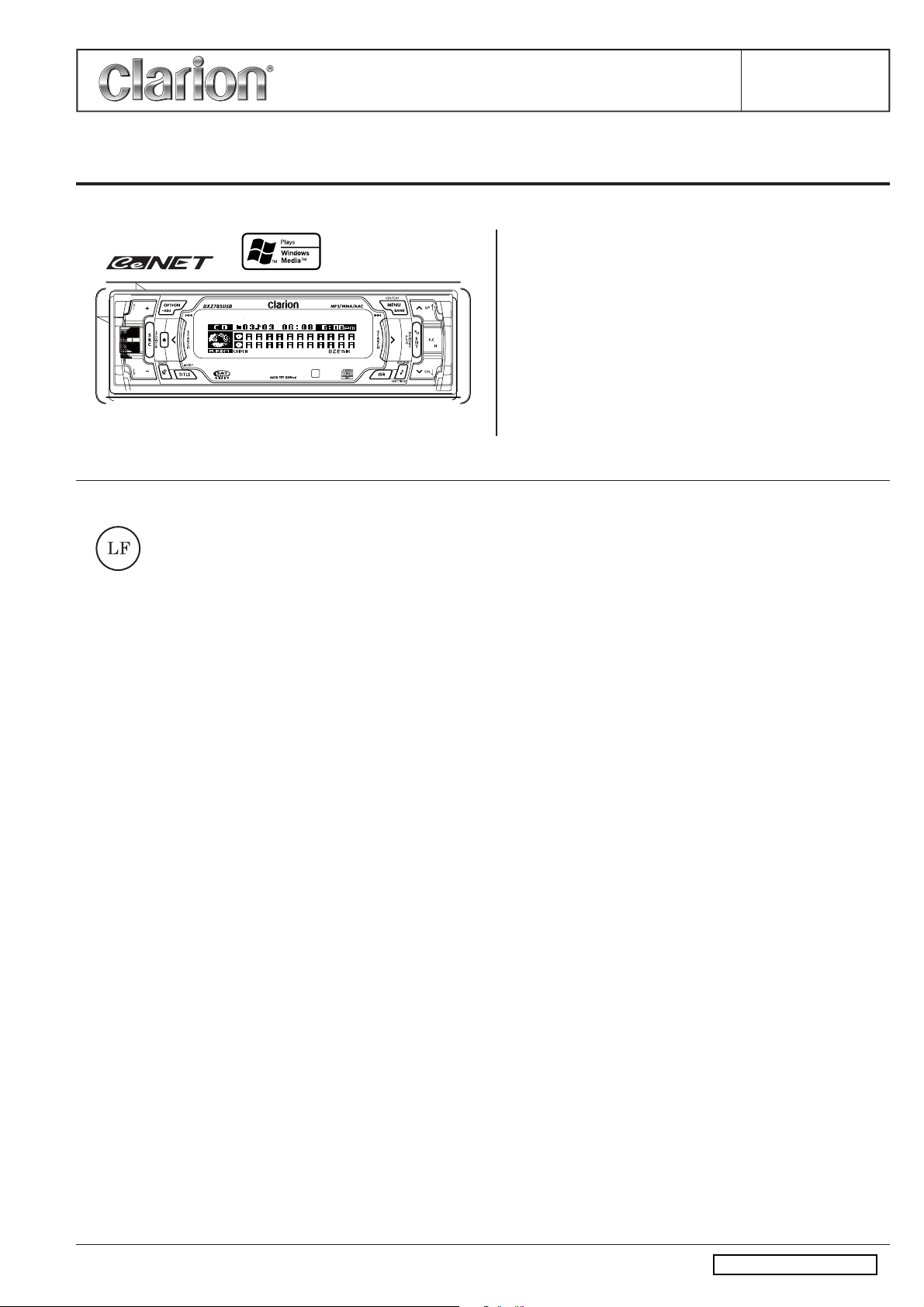
Service Manual
CD/USB/MP3/WMA/AAC Receiver
with CeNET Control
Published by Service Dept.
298-6525-00 JAN. 2008P
Printed in P.R.C.
(DXZ785USB)
This product is a lead free model.
Lead free solder is used in PWB stamped LF mark.
Please keep the following conditions when you repair.
1. Use lead free solder.
* Koki's lead free solder S3X-55M 0.6mm
(CLARION Parts No.642-0231-01)
* Koki's lead free solder S3X-55M 1.0mm
(CLARION Parts No.642-0231-02)
2. Use a nitrogen solder system.
3. Do not use "General solder" and "Lead free solder"
together.
SPECIFICATIONS
FM tuner section
Frequency range: 87.9MHz to 107.9MHz
(PE-3041B-A)
87.0MHz to 108.0MHz
(PE-3041K-A/B)
Usable sensitivity: 9dBf
50dB quieting sensitivity: 15dBf
Alternate channel selectivity: 70dB
Stereo separation: 35dB(1kHz)
Frequency response: 30Hz to 15kHz(+3/-3dB)
AM tuner section
Frequency range: 530kHz to 1710kHz
(PE-3041B-A)
531kHz to 1629kHz
(PE-3041K-A/B)
Usable sensitivity: 25uV
CD player section
System: Compact disc digital audio
system
Usable discs: Compact disc
Model
DXZ785USB
(PE-3041B-A for U.S.A)
Model
DXZ786USB
(PE-3041K-A/B for Other Countries)
Frequency response: 5Hz to 20kHz(+1/-1dB)
Dynamic range: 95dB(1kHz)
Harmonic distortion: 0.01%
MP3/WMA/AAC mode
MP3 Sampling rate: 8kHz to 48kHz
MP3 Bit rate: 8kbps to 320kbps / VBR
WMA Bit rate: 8kbps to 320kbps
AAC Sampling rate: 8kHz to 48kHz
AAC Bit rate: 8kbps to 320kbps / VBR
Logical format: ISO9660 level1, 2
JOLIET or Romeo or APPLE ISO
file system
Audio section
Maximum power output: 53Wx4
Bass control action: +12/-12dB(80Hz)
Treble control action: +12/-12dB(10kHz)
Line output level: 5.8V(CD 1kHz)
General
Power supply voltage: 14.4V DC(10.8 to 15.6V allowable),
negative ground
Current consumption: Less than 15A
Speaker impedance: 4ohm(4ohm to 8ohm allowable)
Weight: Source unit 1.6kg
Remote control unit
40g(including battery)
Dimensions(mm): Source unit
178(W)x50(H)x158(D)
Remote control unit
44(W)x113(H)x11(D)
NOTE
We cannot supply PWB with component parts in principle. When
*
a circuit on PWB has failure, please repair it by component parts
base. Parts which are not mentioned in service manual are not
supplied.
Specifications and design are subject to change without notice for
*
further improvement.
-1-
DXZ785USB/DXZ786USB
Page 2

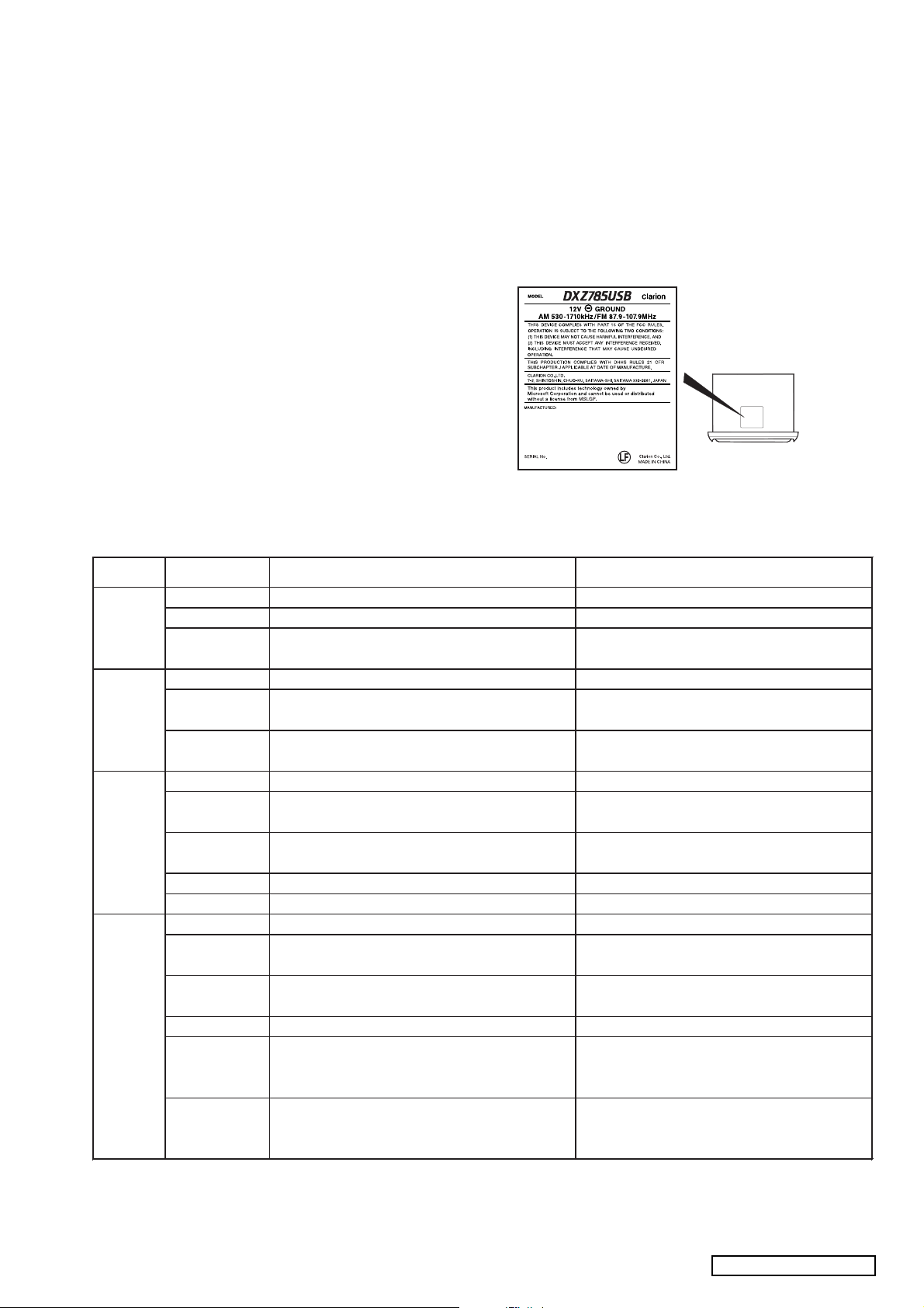
Use only compact discs bearing the or mark.
*
Some CDs recorded in CD-R/CD-RW mode may not be usable.
* Windows Media , and the Windows logo are trademarks, or re-
gistered trademarks of Microsoft Corporation in the United States
and/or other countries.
* WMA is the abbreviation of Windows Media Audio, an audio file
format developed by Microsoft Corporation.
* This product includes technology owned by Microsoft Corporation
and cannot be used or distributed without a license from MSLGP.
* As for this model, the tuner of the DSP type is used.When you
exchange it due to the tuner pack(BL1:880-2091E) trouble, it is
necessary to adjust for S-meter etc.Special JIG is necessary for
an accurate adjustment.The procedure document for the exclusive
use jig is appended to it.
* This DSP IC SAF7730HN219A(051-6706-40) of main PWB is ex-
posed die soldering pad type. The middle of this IC package is so-
ldered with the main PWB, and it cannot remove in an ordinary s-
oldering iron.Please use special removal JIG at the time of IC exc-
hange.
* This unit is compatible with USB 1.1/2.0 with maximum data tran-
sfer rates of 12 Mbps.USB memory devices that can be played by
connecting to the unit's USB connector are limited to those recog-
nized as "USB mass storage class devices"; operation is not gua-
ranteed with all USB memory devices.
* To prevent the accidental loss of data, always back up important
data on your computer.
* This unit does not support connections to a computer.In addition,
connections made through a USB hub device are also not
supported.
* This unit supports USB Digital Media Streaming.USB Digital Media
Streaming is a function used to play music files transmitted using
Media Transfer Protocol (MTP). This function also supports the
playback of WMDRM 10 files.
* Insert and remove a USB memory device only when the device is
not being accessed. Connecting or disconnecting the device at the
following times may result in the loss of data:
- If the USB memory device is removed or power is disconnected
during writing to the device.
* iPod is for legal or rightholder-authorized copying only. Don't st-
eal music. iPod is a trademark of Apple Computer, Inc., registered
in the U.S and other countries.
COMPONENTS
PE-3041B-A/PE-3041K-A/B
1. Source unit 1
2. Remote control unit RCB-176-200 1
3. Battery(CR2025) 1
4. Mounting bracket(PE-3041B-A) 300-8088-00 1
5. Mounting bracket(PE-3041K-A/B) 300-7742-00 1
6. Mounting bracket(PE-3041K-A/B) 300-4976-00 1
7. DCP case 335-6035-04 1
8. Escutcheon(OUT-ES)
9. Extension lead 854-6433-50 1
10. RCA PIN CORD 855-5520-56 1
11. Parts bag
11-1. Removal key 331-2497-00 2
11-2. Part screw(M1.7x6)(PE-3041B-A) 716-0872-61 1
11-3. Screw(M5x8) 716-0496-51 1
11-4. Rubber part 345-3799-20 8
DXZ785USB/DXZ786USB
370-6226-04 1
1
To engineers in charge of repair or inspection of our products.
Before repair or inspection, make sure to follow the
instructions so that customers and Engineers in charge
of repair or inspection can avoid suffering any risk or
injury.
1. Use specified parts.
The system uses parts with special safety features against fire
and voltage. Use only parts with equivalent characteristics
when replacing them.
The use of unspecified parts shall be regarded as remodeling
for which we shall not be liable. The onus of product liability
(PL) shall not be our responsibility in cases where an accident
or failure is as a result of unspecified parts being used.
2. Place the parts and wiring back in their original positions after
replacement or re-wiring.
For proper circuit construction, use of insulation tubes, bond-
ing, gaps to PWB, etc, is involved. The wiring connection and
routing to the PWB are specially planned using clamps to keep
away from heated and high voltage parts. Ensure that they are
placed back in their original positions after repair or inspec-
tion.
If extended damage is caused due to negligence during re-
pair, the legal responsibility shall be with the repairing com-
pany.
3. Check for safety after repair.
Check that the screws, parts and wires are put back securely
in their original position after repair. Ensure for safety reasons
there is no possibility of secondary ploblems around the re-
paired spots.
If extended damage is caused due to negligence of repair, the
legal responsibility shall be with the repairing company.
4. Caution in removal and making wiring connection to the parts
for the automobile.
Disconnect the battery terminal after turning the ignition key
off. If wrong wiring connections are made with the battery con-
nected, a short circuit and/or fire may occur. If extensive dam-
age is caused due to negligence of repair, the legal responsi-
bility shall be with the repairing company.
5. Cautions in soldering
Please do not spread liquid flux in soldering.
Please do not wash the soldering point after soldering.
6. Cautions in soldering for chip capacitors
Please solder the chip capacitors after pre-heating for replace-
ment because they are very weak to heat.
Please do not heat the chip capacitors with a soldering iron
directly.
7. Cautions in handling for chip parts.
Do not reuse removed chips even when no abnormality is ob-
served in their appearance. Always replace them with new
ones. (The chip parts include resistors, capacitors, diodes, tran-
sistors, etc).
Please make an operation test after replacement.
8. Cautions in handling flexible PWB
Before working with a soldering iron, make sure that the iron
tip temperature is around 270
iron tip repeatedly(more than three times)to the same patterns.
Also take care not to apply the tip with force.
9. Turn the unit OFF during disassembly and parts replacement.
Recheck all work before you apply power to the unit.
-2-
. Take care not to apply the
Page 3
10. Cautions in checking that the optical pickup lights up.
Error Display Cause Measure
ERROR 2 A CD is caught inside the CD deck and is not ejected. This is a failure of CD deck’s mechanism.
ERROR 3 A CD cannot be played due to scratches, etc. Replace with a non-scratched, non-warped-disc.
ERROR 6 A CD is loaded upside-down inside the CD deck and Eject the disc then reload it properly.
does not play.
ERROR 2 A CD inside the CD changer is not loaded. This is a failure of CD changer’s mechanism.
ERROR 3 A CD inside the CD changer cannot be played due to Replace with a non-scratched, non-warped disc.
scratches, etc.
ERROR 6 A CD inside the CD changer cannot be played Eject the disc then reload it properly.
because it is loaded upside-down.
ERROR 2 A DISC inside the DVD changer cannot be played. This is a failure of DVD mechanism.
ERROR 3 A DISC cannot be played due to scratches, etc. Retry or replace with a non-scratched,
non-warped disc.
ERROR 6 A DISC inside the DVD changer cannot be played Eject the disc then reload it properly.
because it is loaded upsidedown.
ERROR P Parental level error Set the correct Parental level.
ERROR R Region code error Eject the disc and replace correct region code disc.
ERROR 2 The files are not proper MP3/WMA/AAC format. Use only properly encoded MP3/WMA/AAC files.
ERROR 3 The MP3/WMA/AAC files are improperly encoded. Use only properly encoded MP3/WMA/AAC files.
(USB/MTP mode)
ERROR 3 The iPod contains no audio files. Insert an iPod containing audio files.
(iPod mode)
ERROR 5 The connected devices are not recognized. Disconnect the devices and reconnect.
BUS-PWR Overcurrent detection. Disconnect the devices and reconnect. If the
devices are still not recognized, try replacing with
a different devices.
HUB The connected devices are not recognized. Disconnect the devices and reconnect. If the
devices are still not recognized, try replacing with
a different devices.
CD/MP3/
WMA/AAC
CD
changer
DVD
changer
USB/MTP/
iPod
The laser is focused on the disc reflection surface through the
lens of the optical pickup. When checking that the laser opti-
cal diode lights up, keep your eyes more than 30cms away
from the lens. Prolonged viewing of the laser within 30cms
may damage your eyesight.
11. Cautions in handling the optical pickup
The laser diode of the optical pickup can be damaged by elec-
trostatic charge caused by your clothes and body. Make sure
to avoid electrostatic charges on your clothes or body, or dis-
charge static electricity before handling the optical pickup.
11-1. Laser diode
The laser diode terminals are shorted for transportation in or-
der to prevent electrostatic damage. After replacement, open
the shorted circuit. When removing the pickup from the mecha-
nism, short the terminals by soldering them to prevent this
damage.
11-2. Actuator
The actuator has a powerful magnetic circuit. If a magnetic
material is put close to it. Its characteristics will change. En-
sure that no foreign substances enter through the ventilation
slots in the cover.
11-3. Cleaning the lens
Dust on the optical lens affects performance.
To clean the lens, apply a small amount of isopropyl alcohol to
lens paper and wipe the lens gently.
CAUTION
Use of controls, adjustments, or performance of procedures other
than those specified herein, may result in hazardous radiation ex-
posure.
The compact disc player should not be adjusted or repaired by
anyone except properly qualified service personnel.
276-0379-00
PE-3041B
Bottom view of DXZ785USB
ERROR DISPLAYS
If an error occurs, one of the following displays is displayed. Take the measures described below to eliminate the problem.
* If an error display other than the ones described above appears, press the reset button.
* When the power supply is turned on for the first time, the bolero microcomputer version display is mistake.
It is solved by turning ACC on and off once again.
-3-
DXZ785USB/DXZ786USB
Page 4
TROUBLESHOOTING
Problem Cause Measure
Power does not turn on. Fuse is blown. Replace with a fuse of the same amperage.
(No sound is produced.) Incorrect wiring. Read the attached "Installation/Wire connection Guide" once again
and wire properly.
No sound output when Power antenna lead is shorted to 1. Turn the unit off.
operating the unit with ground or excessive current is 2. Remove all wires attached to the power antenna lead. Check
amplifiers or power required for remote-on the amplifiers each wire for a possible short to ground using an ohm meter.
antenna attached. or power antenna. 3. Turn the unit back on.
4. Reconnect each amplifier remote wire to the power antenna lead
one by one. If the amplifiers turn off before all wires are attached,
an external relay to provide remote-on voltage (excessive current
required).
Nothing happens when The microprocessor has
Turn off the power, then press the [
RELEASE
]
buttons are pressed. malfunctioned due to noise, etc. button and remove the DCP.
Press the reset button for about
Display is not accurate. 2 seconds with a thin rod.
DCP or main unit connectors Wipe the dirt off with a soft cloth moistened with
are dirty. cleaning alcohol.
No sound heard The speaker protection circuit Turn down sound volume. Function can also be restored by
is operating. turning the power off and on again. (Speaker volume is reduced
automatically when the speaker protection circuit operates).
No sound heard MP3/WMA/AAC files are Write MP3/WMA/AAC files onto the disc properly.
absent in a disc.
Files are not recognized as Use MP3/WMA/AAC files encoded properly.
an MP3/WMA/AAC file.
File system is not correct. Use ISO9660 level 1, 2 or JOLIET or Romeo or
APPLE ISO file system.
Sound skips or is noisy. Compact disc is dirty. Clean the compact disc with a soft cloth.
Compact disc is heavily Replace with a compact disc with no scratches.
scratched or warped.
Sound is cut or skipped. MP3/WMA/AAC files are not Use MP3/WMA/AAC files encoded properly.
Noise is generated or encoded properly.
noise is mixed with sound.
Sound is bad directly after Water droplets may form on Let dry for about 1 hour with the power on.
power is turned on. the internal lens when the car
is parked in a humid place.
Wrong filename File system is not correct. Use ISO9660 level 1, 2 or JOLIET or Romeo or
APPLE ISO file system.
No sound heard The device contains no MP3/ Record MP3/WMA/AAC files properly to the device.
WMA/AAC files.
The files are not proper MP3/ Use only properly encoded MP3/WMA/AAC files.
WMA/AAC format.
Connectors are loose. Disconnect the device and reconnect securely.
Sound is interrupted or The MP3/WMA/AAC files are Use only properly encoded MP3/WMA/AAC files.
has noise. improperly encoded.
The device isn’t The device is damaged. Disconnect the device and reconnect. If the device is still not
recognized. Connectors are loose. recognized, try replacing with a different device.
According to the state of operation Disconnect the device and reconnect.
on the device, the communication
fault is caused.
Can’t insert the device. The device has been inserted Try reversing the connection direction of the device
improperly. (usually the brand name surface should be facing left).
The connector is broken. Replace with a new device.
GeneralUSBMTP/iPod CD/MP3/WMA/AAC
Reset button
DXZ785USB/DXZ786USB
-4-
Page 5
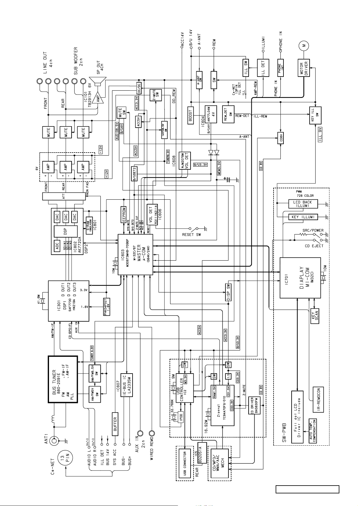
BLOCK DIAGRAM
Main section
Q
CONTROL
RECEPT
RECEPT
BUILT-IN for ALL WORLD
TMP92CD28AFG
-6UP2
FJ
-TR
IC3
M30876MJB-713GP
MECH PWB
IC1
-5-
DXZ785USB/DXZ786USB
Page 6

ADJUSTMENTS
1.Terminal Description
pin 1
:NC:IN:
Ground.
pin 2
:
OEM-REMOCON
:IN:
The steering remote controller signal input.
pin 3
:
IE-BUS-TX
:O:
IE Bus serial data output.
pin 4
:
IE-BUS-RX
:IN:
IE Bus serial data input.
pin 5
:
AUTO-ANT
:O:
Motor antenna signal output.
pin 6
:
BYTE(GND):IN
:
Connect to VSS.
pin 7
:
CNVSS
:IN:
Connect to VSS.
(with internal pull-down resistor)
pin 8
:
XCIN
:IN:
The crystal resonator for sub-clock.
pin 9
:
XCOUT
:IN:
The crystal resonator for sub-clock.
pin 10
:
RESET
:IN:
The reset signal input.
pin 11
:
X-OUT
:O:
The resonator for main clock.
pin 12
:
GND
:-:
Ground.
pin 13
:
X-IN
:IN:
The resonator for main clock.
pin 14
:
VCC1
:-:
Positive power supply.
pin 15
:
VCC
:-:
Positive power supply.
pin 16
:
ACC-DET
:IN:
ACC detection signal input.
pin 17
:
B/U-DET1
:IN:
Backup detection signal input.
pin 18
:
ILL-DET
:IN:
The illumination detection signal input.
pin 19
:
OFFSET-DET:IN
:
The emergency signal input from the power IC.
pin 20
:
E2P-DO
:O:
The serial data output to the E2PROM.
pin 21
:
E2P-SCK
:O:
The clock pulse output to the E2PROM.
pin 22
:
E2P-DI
:IN:
The serial data output to the E2PROM.
pin 23
:
E2P-CS
:O:
E2PROM chip selection signal output.
pin 24
:NC:IN:
Ground.
pin 25
:NC:IN:
Ground.
pin 26
:NC:IN:
Ground.
pin 27
:
TUN-SCL
:O:
The clock pulse output to the BUS tunner.
pin 28
:
TUN-SDA
:
I/O
:
The serial data input/output to the BUS tunner
pin 29
:
FLASH TX
:O:
The flash serial data output.
pin 30
:
FLASH RX
:IN:
The flash serial data input.
pin 31
:
FLASH-SCL:IN
:
Ground.
pin 32
:
FLASH-BUSY:O
:
Not in use.
pin 33
:
BOLERO-SDA:I/O
:
The serial data input/output to the BOLERO.
pin 34
:
BOLERO-SCL:O
:
The clock pulse output when to the BOLERO.
pin 35
:
Z-MUTE-CUT:O:The cut of contral signal output to the MUTE.
(CD:H:no cut; out of CD:L:cut)
pin 36
:
A-MUTE(TEST):IN
:
Test pin.
pin 37
:
EMPH
:O:
Test pin.
052-3977-10 M30873MHB-709GP Main System controller
pin 38
:
BOLERO-RESET
:O:
The reset signal output of the BOLERO.
pin 39
:
FLASH-EPM:IN
:
Ground.
pin 40
:NC:IN:
Not in use.
pin 41
:NC:IN:
Not in use.
pin 42
:NC:IN:
Not in use.
pin 43
:
CATS-LED
:O:
CATS LED drive output.
pin 44
:
FLASH-CE
:IN:
The serial data output for the flash memory.
pin 45
:NC:O:
Not in use.
pin 46
:NC:IN:
Not in use.
pin 47
:NC:IN:
Not in use.
pin 48
:NC:IN:
Not in use.
pin 49
:NC:IN:
Not in use.
pin 50
:
BOLERO-REQ:IN
:
The request signal input to the BOLERO.
pin 51
:
AMP-MUTE
:O:
Muting signal output to the
Audio Power Amplifier.
pin 52
:NC:
I/O
:
Not in use.
pin 53
:NC:O:
Not in use.
pin 54
:NC:O:
Not in use.
pin 55
:
DSP-RESET:O
:
Reset signal output to the DSP IC.
pin 56
:
DSP-INIT
:IN:
The initial finished signal input from the
Radio-Audio-DSP.
pin 57
:
AMP-STBY
:O:
ON signal output to the internal Amplifier.
pin 58
:
EXT-AMP-REM:O
:
ON signal output to the external Amplifier.
pin 59
:
NOISE-CUT:O
:
The cut of contral signal output to the noise.
pin 60
:
VCC
:-:
Positive power supply.
pin 61
:NC:IN:
Ground.
pin 62
:
GND
:-:
Ground.
pin 63
:
AM/FM-ON
:O:
The 8.5V power supply ON signal output.
pin 64
:
AM/FM-5V-ON:O
:
The 5V power supply ON signal output.
pin 65
:
DSP2-INIT
:O:
The initial reset signal output to DSP2.
pin 66
:
DSP2-RESET:O
:
The reset pulse output to DSP2.
pin 67
:
DSP2-REQ
:O:
The request signal output to DSP2.
pin 68
:
DSP2-SCK
:O:
The clock pulse output to DSP2.
pin 69
:
DSP2-SO
:O:
The serial data output to DSP2.
pin 70
:
DSP2-RDY
:IN:
The ready signal input to DSP2.
pin 71
:
KEY-INT
:IN:
Key interrupting signal input.
pin 72
:
B/U-DET2
:IN:
Backup detection signal input.
pin 73
:
BOLERO-ACC:O
:
The ACC signal of the BOLERO.
pin 74
:
PHONE-IN
:IN:
The telephone interrupt signal input.
pin 75
:
AMP-REM-DET:IN
:
Remote controller wire short detection.
pin 76
:
MOTOR+
:O:
The control signal output to the motor.
pin 77
:
MOTOR-
:O:
The control signal output to the motor.
pin 78
:NC:IN:
Ground.
ADJUSTMENT OF BUS-TUNER : 880-2091E
This adjustment sets some values of the tuner.The adjustment
data is written in EEPROM(IC605).The special jig and software
are necessary for this adjustment.
* CeNET-analyzer
* Personal computer
*SG
* Adjustment-Software:Adjustment system for DSP N217
with CeNET(Ver.Y4-S024-103-20060623)
Preparation
1. Installation of software
Execute the windows installer package in the set-folde
of the writing E2P.
PRN data writing
1) Click [prn FILE LOAD], and select PRN-FILE.
2) Click [EEPROM WRITE], the PRN-data is write in EEPROM
of the unit.
Adjustments
1. FM S-meter
1) Set SG output to 65dBuV.(FM)
2) Click [Adjustment] of "FM S-Meter".(Wait until the value stops.)
2. FM IF-Count
1) Click [Adjustment] under "FM IF-COUNT".(The FM-IFOffset data of EEPRON is effective.)
2) Click [Check], and confirm the display is within +/-500.0.
2. Connection
1) Connect CeNET-analyzer to the unit with the CeNET-cable.
2) Connect CeNET-analyzer(MASTER/SLAVE side) to the
PC with the serial crossing cable.
3) Connect POWER-lead of CeNET-analyzer to the
POWER-lead of the unit.
4) Connect the antenna to the unit.(FM-ANT for first adjustment)
5) Turn on CeNET-analyzer,and press the RESET-button of it.
Set up the software
1) Click [ADJ_DSP].
2) Click [open Comm PORT].(To open the COM port of PC)
3) Click [Initialization of JIG].(The BUS-analyzer sounds)
4) Click [Incoming connection].(The unit is recognized to
the BUS-analyzer)
The data is displayed, and the display changes regularly.
EXPLANATION OF IC
Main section
DXZ785USB/DXZ786USB
3. Set up AM IF Offset data
* Exchange the antenna for "AM-ANT-dummy"
1) Click [Adjustment] under "AM IF-COUNT".(The AM-IFOffset data of EEPRON is effective.)
2) Click [Check], and confirm the display is within +/-500.0.
4. AM S-meter
1) Set SG output to 70dBuV.(AM)
2) Click [Adjustment] of "AM S-Meter".(Wait until the value stops.)
Finally, push the reset button of the unit.
When computer continues to freeze, click [RESET] of "MENU", and
readjust the lost adjustment point.IF not returning, press the
RESET-button of CeNET-analyzer.and restart adjustment from
the first step.
-6-
Page 7

pin 79
:
CLOSE-POSI:IN
:
The close position detect signal input.
pin 80
:
OPEN-POSI:IN
:
The open position detect signal input.
pin 81
:
ILL-DET-OUT:O
:
Illumination ON signal output.
pin 82
:
DISP-REM
:O:
The power supply control signal output for the
displayer.
pin 83
:NC:IN:
Ground.
pin 84
:
DD-REM
:O:
pin 85
:
DD-F-SW
:O:
The frequency control signal output
for DC_DC_Converter.
pin 86
:
MOTOR-REM:O
:
Motor power ON signal output.
pin 87
:
KEY-ILL-REM:O
:
The key illumination ON signal output.
pin 88
:
DISP-RESET:O
:
Display reset signal output.
pin 89
:
KEY-A/D
:IN:
The input terminal of the internal ADC
for key judgment.
pin 90
:
SYS-ACC
:O:
ACC detection signal input.
pin 91
:
SYS-MUTE
:O:
System muting signal output.
pin 92
:
INT1
:IN:
The destination setting input.
pin 93
:
INT2
:IN:
The destination setting input.
pin 94
:
AVSS(GND)
:-:
Negative voltage supply for A/D converter.
pin 95
:
TEST
:O:
Test pin.
pin 96
:
VREF
:IN:
Reference vlotage input for A/D converter .
pin 97
:
AVDD
:-:
Positive voltage supply for A/D converter.
pin 98
:
DSP-SCL
:O:
I2BUS serial clock output
for the Radio-Audio-DSP.
pin 99
:
DSP-SDA
:
I/O
:
I2BUS serial data input/output
for the Radio-Audio-DSP.
pin100:NC
:IN:
Ground.
1.Terminal Description
pin 1
:
LCD-ON
:O:
LCD power supply.
pin 2
:
INT1
:IN:
The destination setting input.
pin 3
:
IE-BUS-TX
:O:
IE Bus serial data output.
pin 4
:
IE-BUS-RX
:IN:
Bus serial data input.
pin 5
:
REMOCON
:IN:
Remote controller signal input terminal.
pin 6
:
BYTE(GND)
:IN:
Connect to VSS.
pin 7
:
CNVSS
:IN:
Connect to VSS.
pin 8
:NC:IN:
Ground.
pin 9
:NC:IN:
Ground.
pin 10
:
RESET
:IN:
The reset signal input.
pin 11
:
X-OUT
:O:
The resonator for main clock.
pin 12
:
GND
:-:
Ground.
pin 13
:
X-IN
:IN:
The resonator for main clock.
pin 14
:
VCC
:-:
Positive power supply.
pin 15
:
VCC
:IN:
Positive power supply.
pin 16
:
SYS-ACC-IN
:IN:
ACC detect signal output.
pin 17
:NC:IN:
Ground.
pin 18
:NC:IN:
Ground.
pin 19
:NC:IN:
Ground.
pin 20
:
VARI-BLUE
:O:
Variable blue.
pin 21
:NC:IN:
Ground.
pin 22
:
VARI-GREEN
:O:
Variable green.
pin 23
:
BACK-L-ON
:O:
The backlight control signal output.
pin 24
:
VARI-RED
:O:
Variable red.
pin 25
:
KEY-ILL
:O:
The key illumination ON signal output.
pin 26
:NC:IN:
Ground.
pin 27
:NC:IN:
Ground.
pin 28
:
LCD-CS
:O:
Chip select signal output to LCD.
pin 29
:
FLASH TX
:O:
The serial data output for flash memory.
pin 30
:
FLASH RX
:IN:
The serial data input for flash memory.
pin 31
:
FLASH-SCL
:IN:
Ground.
pin 32
:
FLASH-BUSY
:O:
Not in use.
pin 33
:
LCD-SI
:O:
The serial data input to the LCD driver.
pin 34
:
LCD- AO
:O:
LCDdriverdatatypecontrol.
pin 35
:
LCD-CLK
:O:
The clock pulse output to the LCD driver.
pin 36:LCD-RESET
:O:
LCD driver reset signal output.
pin 37
:NC:IN:
Ground.
pin 38
:NC:IN:
Ground.
pin 39
:
FLASH-EPM
:IN:
Ground.
pin 40
:NC:IN:
Ground.
pin 41
:NC:IN:
Ground.
pin 42
:NC:IN:
Ground.
pin 43
:NC:IN:
Ground.
pin 44
:
FLASH-CE
:IN:
The chip enable signal input for flash memory
pin 45
:NC:IN:
Ground.
pin 46
:NC:IN:
Ground.
pin 47
:NC:IN:
Ground.
pin 48
:NC:IN:
Ground.
052-7302-10 M30876MJB-713GP Switch System controller
pin 49:KO0
:O:
Key scanning output terminal.
pin 50
:
KO1
:O:
Key scanning output terminal.
pin 51
:
KO2
:O:
Key scanning output terminal.
pin 52
:
KO3
:O:
Key scanning output terminal.
pin 53
:NC:IN:
Ground.
pin 54
:NC:IN:
Ground.
pin 55
:
KI0
:IN:
Key scanning intput terminal.
pin 56
:
KI1
:IN:
Key scanning intput terminal.
pin 57
:
KI2
:IN:
Key scanning intput terminal.
pin 58
:
KI3
:IN:
Key scanning intput terminal.
pin 59
:NC:IN:
Ground.
pin 60
:
VCC
:-:
Positive power supply.
pin 61
:NC:IN:
Ground.
pin 62
:
GND
:-:
Ground.
pin 63
:NC:IN:
Ground.
pin 64
:NC:IN:
Ground.
pin 65
:NC:IN:
Ground.
pin 66
:NC:IN:
Ground.
pin 67
:NC:IN:
Ground.
pin 68
:NC:IN:
Ground.
pin 69
:NC:IN:
Ground.
pin 70
:NC:IN:
Ground.
pin 71
:NC:IN:
Ground.
pin 72
:NC:IN:
Ground.
pin 73
:
ILL-DET
:IN:
The illumination detection signal input.
pin 74
:NC:IN:
Ground.
pin 75
:NC:IN:
Ground.
pin 76
:NC:IN:
Ground.
pin 77
:NC:IN:
Ground.
pin 78
:NC:IN:
Ground.
pin 79
:NC:IN:
Ground.
pin 80
:NC:IN:
Ground.
pin 81
:NC:IN:
Ground.
pin 82
:NC:IN:
Ground.
pin 83
:NC:IN:
Ground.
pin 84
:NC:IN:
Ground.
pin 85
:NC:IN:
Ground.
pin 86
:NC:IN:
Ground.
pin 87
:NC:IN:
Ground.
pin 88
:NC:IN:
Ground.
pin 89
:NC:IN:
Ground.
pin 90
:NC:IN:
Ground.
pin 91
:NC:IN:
Ground.
pin 92
:NC:IN:
Ground.
pin 93
:NC:IN:
Ground.
pin 94
:
AVSS(GND)
:-:
Negative voltage supply for A/D converter .
pin 95
:NC:IN:
Ground.
pin 96
:
VREF
:IN:
Reference vlotage input for A/D converter .
pin 97
:
AVDD
:-:
Positive voltage supply for A/D converter.
pin 98
:NC:IN:
Ground.
pin 99
:NC:IN:
Ground.
pin100
:NC:IN:
Ground.
pin 1
:
VCC
:-:
Supply volltage positive terminal.
pin 2
:
XIN
:-:
32.768 kHz crystal oscillator or external
clock sourcer.
pin 3
:
XOUT
:-:
32.768 kHz crystal oscillator or external
clock sourcer.
pin 4
:
CLOCK_ENAB
:I:
CLOCK_OUT enable(active high).
pin 5
:NC:-:
Not in use.
pin 6
:NC:-:
Not in use.
pin 7
:
I2C_SCL
:
I/O
:
I C clock.
pin 8
:
I2C_ADDR0
:I:
I C slave address selection
pin 9
:
I2C_ADDR1
:I:
I C slave address selection
pin 10
:
I2C_ADDR2
:I:
I C slave address selection
pin 11
:
CP_READY
:O:
CP ready to receive next instruction
(active high).
pin 12
:
MODE0
:I:
Operating voltage selection.
pin 13
:
MODE1
:I:
Communication mode selection.
pin 14
:NC:-:
Not in use.
pin 15
:
I2C_SDA
:
I/O
:
ICdata.
pin 16
:
MODE2
:I:
Communication mode selection.
pin 17
:
ROSC
:I:
Connect via 100k¡1% resistorto VCC.
pin 18
:
SPI_nSS
:I:
SPI slave select (active low).
pin 19
:
SPI_SIMO
:I:
SPI master-to-slave data.
pin 20
:
SPI_SOMI
:O:
SPI slave-to-master data.
pin 21
:
SPI_UCLK
:I:
SPI clock.
051-6928-90 341S2094 iPod Authentication Coprocessor Specification
The control signal output for DC_DC_Converter.
-7-
2
2
2
2
2
DXZ785USB/DXZ786USB
Page 8

NO. PART NO. DESCRIPTION Q'TY NO. PART NO. DESCRIPTION Q'TY
1 ----------- SENSOR PWB 1 39 621-1750-20 POWER GEAR C 1
2 966-1743-21 DRIVE-PLT-ASSY 1 40 621-1751-20 POWER GEAR D 1
3 SMA-182-100 SPINDLE MOTOR-ASSY 1 41 621-1752-20 DISC STOPPER 1
4 SMA-197-100 SLED MOTOR-ASSY 1 42 621-1753-20 CLAMPER RING 1
5 345-5476-20 CUSHION RUBBER 1 43 621-1754-20 GEAR BASE 1
6 620-1023-23 CLAMPER PLATE 1 44 622-1571-21 ROLLER SHAFT 1
7 620-1026-21 SPRING PLATE 1 45 624-0020-00 LEAD SCREW 1
8 620-1596-23 CLAMPER LINK 1 46 629-0081-21 DAMPER F 2
9 620-1598-22 UPPER CHASSIS 1 47 629-0082-21 DAMPER R 1
10 620-1752-20 SENSOR ARM 1 48 716-1507-01 SCREW(M2x3) 1
11 620-1753-20 ID-LOCK PLATE 1 49 716-1670-01 SCREW(M2x4) 4
12 620-1766-20 LOWER CHASSIS 1 50 716-1733-01 SCREW(M1.7x2.3) 2
13 621-0608-21 SECOND GEAR 1 51 716-3469-01 SCREW(1.7x4) 2
14 621-0609-20 BASE GEAR 1 52 716-3473-01 SCREW(M2x3) 1
15 621-0610-20 IDLE GEAR A 1 53 716-3551-00 SCREW(M1.4x2.5) 2
16 621-0611-20 IDLE GEAR B 1 54 750-7865-20 SHIFT SPRING 1
17 621-0612-21 ROLLER GEAR A 1 55 750-7866-20 RACK SPRING 1
18 621-0620-20 THREAD GEAR A 1 56 750-7867-20 CLAMPER SPRING 1
19 621-0621-20 THREAD GEAR B 1 57 750-7868-20 ID-LOCK SPRING 1
20 621-0623-23 LS-HOLDER 1 58 750-7869-20 SENSOR SPRING 1
21 621-0624-22 GUIDE RAIL 1 59 750-7870-20 DR-SPRING F 2
22 621-0711-21 LOADING ROLLER 2 60 750-7871-20 DR-SPRING RA 1
23 621-0718-21 ROLLER GUIDE 1 61 750-7872-20 DR-SPRING RB 1
24 621-0719-20 ROLLER GEAR 1 62 750-7873-20 DR-SPRING C 1
25 621-0720-20 ROLLER GEAR C 1 63 750-6797-20 ROLLER SPRING L 1
26 621-0721-20 ROLLER GEAR D 1 64 750-6798-20 ROLLER SPRING R 1
27 621-0728-20 STOPPER LINK 1 65 714-2003-8B SCREW(M2x3) 2
28 621-1719-20 IDLE CASE 1 66 780-2025-00 SCREW(M2x2.5) 3
29 621-1726-20 ROLLER SLEEVE 2 67 781-1730-00 SCREW(M1.7x3) 1
30 621-1729-20 SH-BASE 1 68 803-4906-60 VINYL-COAT-WIRE(ORG) 1
31 621-1742-20 UPPER GUIDE 1 69 969-0071-30 PICKUP-ASSY 1
32 621-1743-20 SHIFT LEVER 1 70 816-2590-00 SPECIAL LEAD(GRN) 1
33 621-1744-20 RACK 1 71 816-2591-00 SPECIAL LEAD(YEL) 1
34 621-1745-20 LOCK ARM L 1 72 816-2592-00 SPECIAL LEAD(BLUE) 1
35 621-1746-20 LOCK ARM R 1 73 816-2593-00 SPECIAL LEAD(PUR) 1
36 621-1747-20 GEAR COVER 1 74 966-1722-20 SH-RACK-ASSY 1
37 621-1748-20 POWER GEAR A 1 75 816-2624-50 FLAT WIRE 1
38 621-1749-20 POWER GEAR B 1
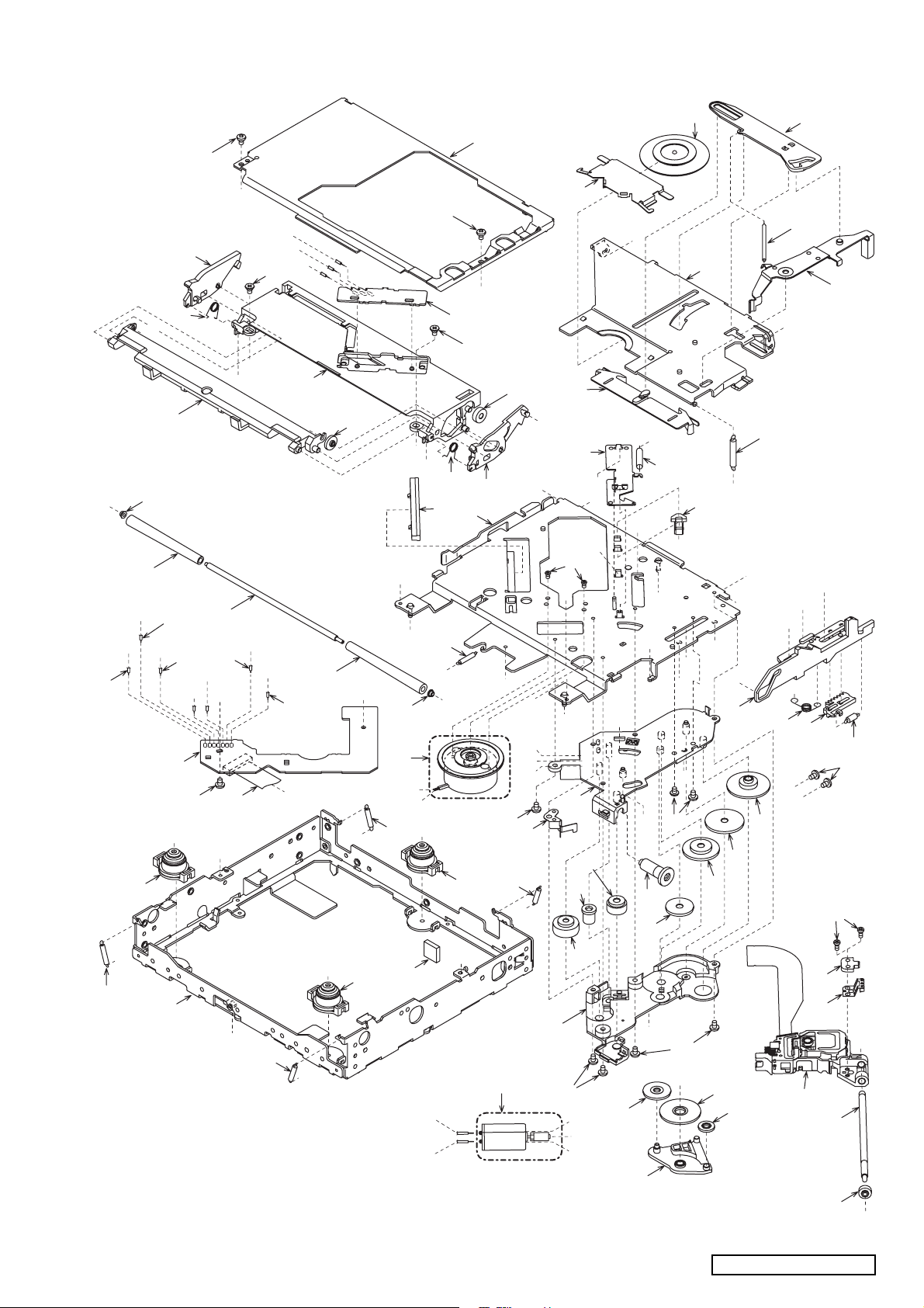
EXPLODED VIEW / PARTS LIST
pin 22
:NC:-:
Not in use.
pin 23
:NC:-:
Not in use.
pin 24
:NC:-:
Not in use.
pin 25
:NC:-:
Not in use.
pin 26
:NC:-:
Not in use.
pin 27
:NC:-:
Not in use.
pin 28
:NC:-:
Not in use.
pin 29
:NC:-:
Not in use.
pin 30
:NC:-:
Not in use.
pin 31
:NC:-:
Not in use.
pin 32
:
CLOCK_OUT
:O:
32.768 kHz clock output, if selected by
CLOCK_ENAB.
pin 33
:NC:-:
Not in use.
pin 34
:NC:-:
Not in use.
pin 35
:NC:-:
Not in use.
pin 36
:NC:-:
Not in use.
pin 37
:NC:-:
Not in use.
pin 38
:
nRESET
:I:
CP reset(active low).
pin 39
:
VSS
:-:
Supply voltage, negative terminal.
pin 40
:
VCC
:-:
Supply volltage positive terminal.
CD mechanism section: 929-5016-80
DXZ785USB/DXZ786USB
-8-
* The exploded view is on page 9
Page 9
65
42
27
9
B1
71
H1
46
H2
22
B2
29
H3
23
73
A1
34
63
1
72
48
H4
H5
44
G6
A4
68
75
A4
D1
G13
H6
H7
52
H3
H1
H2
70
to MAIN
31
B1
22
G2
26
H6
G13
60
29
G12
A1
3
H5
H4
A3
D2
65
21
62
A8
64
B2
1
47
67
2
A5
35
G6
66
61
25
G3
K1
C3
K2
7
E2
G12
M1
A2
41
50
43
18
6
11
G14
G14
K3
K4
17
G2
C2
E2
G5
C1
24
37
G4
G5
A3
57
66
G1
G9
C5
G8
8
20
G11
38
M1
32
G4
39
E1
G3
40
56
54
K3
58
10
E1
G11
G8
G9
C5
33
55
53
K4
51
59
D1
12
A8
59
D2
A2
46
5
A5
13
30
74
H6
H7
36
4
49
K1
C3
K2
16
H6
C1
49
14
15
G1
69
45
28
19
C2
-9-
DXZ785USB/DXZ786USB
Page 10

DCP section
NO. PART NO. DESCRIPTION Q'TY NO. PART NO. DESCRIPTION Q'TY
1 DCP-607-600 DCP ASSY(PE-3041B-A) 1 1-25 345-8647-00 CUSHION 1
DCP-629-800 DCP ASSY(PE-3041K-A/B) 1 1-26 347-6977-00 COVER FILM 1
1-1 335-7724-00 BRAND 1 1-27 335-7992-00 SPRING CVR 1
1-2 373-1125-10 SEEK PLATE(PE-3041B-A) 1 1-28 335-7984-00 IR FILTER 1
373-1125-24 SEEK PLATE(PE-3041K-A/B) 1 1-29 750-6720-00 SPRING (REL) 1
1-3 947-0738-00 VOLUME BARS 1 1-30 382-8167-00 RELEASE BUTTON 1
1-4 947-0737-00 SIDE PARTS ASSY 1 1-31 001-7088-90 DIODE 4
1-5 750-6856-00 SPRING 1 1-32 347-8245-00 LEATHER SHEET 1
1-6 347-8210-00 TRIM CVR 2 1-33 347-8246-00 LEATHER SHEET 1
1-7 716-0872-51 SCREW(M1.7x6) 6 1-34 347-8251-00 FILM 6
1-8 335-8004-01 ROLLER 2 1-35
347-7347-00 SPACER FILM 1
1-9 370-6260-14 ESCUTCHEON(PE-3041B-A) 1 1-36 347-8249-00 DOUBLE FACE 4
370-6260-16
ESCUTCHEON(PE-3041K-A/B)
1 1-37 347-8252-00 FILM 2
1-10 335-7989-00 SPRING CAP 6 1-38 347-8208-00 LEATHER SHEET 4
1-11 750-6825-00 SPRING 2 1-39 331-4373-00 LCD COVER 1
1-12 335-8005-00 SPRING CVR 2 1-40 347-8213-00 SHAFD 1
1-13 382-8169-04 BUTTON(ISR) 1 1-41 379-1381-81 INDICATOR(LCD) 1
1-14 382-8165-00 BUTTON(ENT) 1 1-42 347-8212-00 FILM 1
1-15 382-8166-02 BUTTON(SOUND) 1 1-43 347-8211-00 FILM 1
1-16 335-7985-00 INDICATOR-A 2 1-44 335-7351-00 ILLUMI PLATE 1
1-17 335-7987-00 ILLUMI PLATE(R) 1 1-45 335-7988-00 LCD HOLDER 1
1-18 335-6899-02 REAR CVR 1 1-46 060-4017-90 IR-RECIEVER 1
1-19 347-6628-00 SPACER FILM 1 1-47 ------------- SWITCH PWB 1
1-20 716-0872-62 SCREW(M1.7X6) 5 1-48 076-0708-02 PLUG 2
1-21 335-7986-01 ILLUMI PLATE(L) 1 1-49 013-6524-50 TACT SWITCH 9
1-22 382-8164-02 BUTTON(EJECT) 1 1-50 013-7419-00 SWITCH 3
1-23 382-8163-00 BUTTON(SRC) 1 1-51 074-2226-71 OUTLET SOCKET(21P) 1
1-24 382-8168-02 BUTTON(TITLE) 1 1-52 076-0647-00 PLUG (16P) 1
1-36
1-29
1-30
1-4
A
A
1-38
1-3
1-33
1-1
1-2
A
: SANKOL application
B
: Grease application
Note) SANKOL uses G-311S
Grease uses CFD-409Z
1-8
1-16
1-34
1-6
1-10
1-7
1-32
1-38
1-12
1-37
1-20
1-26
1-25
1-23
1-22
B
B
1-19
1-7
1-27
1-5
1-11
1-10
1-35
A
1-10
A
1-24
1-13
1-28
1-16
1-21
1-15
B
1-11
1-50
1-12
B
1-14
1-17
1-49
1-7
1-49
1-18
1-20
1-52
1-31
1-50
1-46
1-31
1-48
1-51
1-50
1-47
1-6
1-7
1-8
1-36
1-9
1-49
1-31
1-45
1-44
1-43
1
1-42
1-39
1-41
1-40
Note) Some parts depend on each model.
The model name is specified in the
description.
DXZ785USB/DXZ786USB
-10-
Page 11

Inner escutcheon section
Finished figure
33
36
Grease
application
33
Grease
application
34
35
application
28
Grease
12
12
18
19
10
11
9
Grease
application
37
33
20
8
12
17
26
32
Grease
application
30
29
38
8
31
41
8
26
Grease
application
8
13
12
6
22
8
12
3
2
40
39
4
23
21
24
25
12
5
7
8
16
15
12
Grease
14
1
12
27
application
Note): Grease uses FLOIL 31SB
NO. PART NO. DESCRIPTION Q'TY NO. PART NO. DESCRIPTION Q'TY
1 370-5935-07 INNER ESCUTCHEON 1
2 074-1278-01 OUTLET SOCKET(16P) 1
3 347-6528-00 INSULATOR 1
4 039-2409-05 INNER ES FPC 1
(WITHOUT COMPONENT)
5 331-3115-01 DCP HOLDER 1
6 335-6903-00 ARM-COVER(L) 1
7 335-6904-00 ARM-COVER(R) 1
8 716-1468-70 SCREW(M2x2.5) 10
9 335-7484-00 HOOK 1
10 750-3431-02 SPRING(HOOK) 1
11 341-1802-00 SHAFT 1
12 716-1715-52 DECO-SCREW(M2) 11
13 335-6499-00 CN-CVR 1
14 331-3117-01 LEVER-UP(R) 1
15 331-3118-01 LEVER-LO(R) 1
16 335-6505-00 ILLUMI PLATE 1
17 331-3119-00 LEVER-LO(L) 1
18 331-3120-00 LEVER-UP(L) 1
19 716-1758-50 PAD SCREW(M2x5) 2
20 341-1740-00 ROLLER(ARM) 1
21 347-6527-01 CUSHION 1
22 750-3457-00 SPRING 1
23 291-0102-02 STICKER 1
24 345-8627-01 CUSHION 1
25 346-0150-02 LEATHER SHEET 1
26 716-0872-50 PAD SCREW(M1.7x5) 4
27 750-3304-20 SPRING(GEAR) 1
28 854-4380-01 EXTENSION LEAD 1
29 309-0772-02 FRONT PLATE 1
30 613-0719-00 ARM GEAR 1
31 750-3432-00 SPRING(MOTO) 1
32 613-0733-00 HUS-GEAR 1
33 746-0768-70 SPECIAL WASHER 4
34 613-0717-00 INPUT GEAR 1
35 634-0024-00 MOTOR-ASSY 1
36 947-0513-04 T-LIM-GEAR-ASSY 1
37 750-3303-20 SPRING(ARM) 1
38 347-8262-00 FILM(FRONT) 1
39 345-5937-00 CUSHION 1
40 347-7347-00 SPACER 1
41 946-0079-01 GEAR-BOX ASSY 1
-11-
DXZ785USB/DXZ786USB
Page 12

Main section
NO. PART NO. DESCRIPTION Q'TY NO. PART NO. DESCRIPTION Q'TY
1 076-0312-02 PLUG(2P) 1 28 313-1923-00 HEAT SINK 1
2 013-7206-50 DETECTOR SWITCH 1 29 714-3006-8B MACHINE SCREW(M3x6) 7
3 013-7106-00 DETECTOR SWITCH 1 30 074-1138-65 OUTLET SOCKET(15P) 1
4 331-3378-00 SW-HOLDER 1 31 076-0478-55 PLUG(5P) 1
5 880-2091E TUNER 1 32 074-1228-79 OUTLET SOCKET(29P) 1
6 074-1138-79 OUTLET SOCKET(29P) 1 3 3 074-1138-60 OUTLET SOCKET(10P) 1
7 074-1214-50 OUTLET SOCKET(16P) 1 34 ------------- YAMATO PWB 1
8 331-3954-00 IC-HOLDER 1 35 331-2744-00 STOPPER 1
9 076-0368-16 PLUG(16P) 1 36 347-7581-10 CUSHION 2
10 076-6003-18 PLUG(18P) 1 37 303-0472-07 UPPER-CVR 1
11 074-1194-00 OUTLET SOCKET(CeNET) 1 38 347-7579-10 INSULATOR 1
12
347-6215-00 SPACER-FILM 1
39 714-2603-8B MACHINE SCREW(M2.6x3) 7
13 313-1924-00 HEAT SINK 1 40 331-3324-00 CD-SUB-BRKT(R) 1
14 714-3005-8B MACHINE SCREW(M3x5) 4 41 347-8269-00 SPACER 2
15 305-0348-00 SIDE-CVR(R) 1 42 929-5016-80 CD-MECH-MODULE 1
16 013-6100-00 TACT SWITCH 1 43 716-1670-01 SCREW(M2x4) 2
17 ------------- MAIN PWB 1 44 816-4026-50 FLAT WIRE 1
18 001-7062-90 DIODE 1 45 331-4367-00 MECH BRKT(F) 1
19 305-0347-00 SIDE-CVR(L) 1 46 347-6536-00 PROTECT SHEET 1
20
347-8250-00 DOUBLE FACE 1
47 347-7578-10 INSULATOR 1
21 092-2215-50 ANT-RECEPT 1 48 304-0483-00 LOWER-CVR 1
22 074-1198-68 OUTLET SOCKET(18P) 1 49 276-0379-00 SETPLATE(PE-3041B-A) 1
23 307-0723-01 REAR-CVR 1 276-0413-00 SETPLATE(PE-3041K-A) 1
24 074-0898-16 OUTLET SOCKET(16P) 1 276-0414-00 SETPLATE(PE-3041K-B) 1
25 ------------- D/D PWB 1 50
716-0717-60 STEEL SCREW(M2.3x0.4P) 2
26 855-0613-53 USB CABLE 1 51
780-2005-50 SCREW(M2x5) 2
27 731-3006-8B TAPTIGHT(M3x5) 9 52
345-8701-00 CUSHION 1
It attaches in
the open position.
50
51
50
39
20
44
27
46
42
41
39
45
27
29
31
43
26
5
21
40
39
33
28
30
41
39
38
39
34
32
27
27
43
29
37
27
8
7
25
35
36
Inner escutcheon
19
52
4
3
2
9
10
11
24
23
29
13
1
22
18
49
48
47
DXZ785USB/DXZ786USB
12
17
16
-12-
14
6
15
27
14
Page 13

ELECTRICAL PARTS LIST
REF No. PART No. DESCRIPTION REF No. PART No. DESCRIPTION REF No. PART No. DESCRIPTION
ANT1
092-2215-50
ANT-RECEPT C314 043-1804-90 0.1uF C380 043-1735-90 100pF
BL1 880-2091E TUNER C315 043-1735-90 100pF C382 043-1611-90 2200pF
C2 043-1719-90 22pF C316 043-1735-90 100pF C382 046-2222-58 2200pF
C3 042-1631-50 10V 100uF C317 043-1735-90 100pF C383 043-1611-90 2200pF
C4 043-1802-90 0.01uF C318 043-1802-90 0.01uF C383 046-2222-58 2200pF
C5 043-1821-90 0.022uF C320 043-1804-90 0.1uF C384 043-1819-90 2200pF
C7 043-1800-90 1000pF C321 043-1735-90 100pF C385 043-1819-90 2200pF
C8 187-4763-15 6.3V 47uF C322 042-0654-52 6.3V 10uF C386 043-1819-90 2200pF
C9 043-1608-90 0.1uF C324 043-1804-90 0.1uF C387 043-1819-90 2200pF
C9 046-1042-78 0.1uF C325 043-0552-90 6.3V 47uF C402 042-1563-71 16V 100uF
C10 043-1804-90 0.1uF C327 043-1824-91 0.22uF C409 042-1563-71 16V 100uF
C11 043-1739-90 150pF C327 168-2245-79 0.22uF C410 043-1804-90 0.1uF
C12 043-1735-90 100pF C329 043-0540-00 6.3V 10uF C411 043-0540-00 6.3V 10uF
C13 043-1735-90 100pF C330 043-1841-90 0.047uF C412 043-0540-00 6.3V 10uF
C14 043-1800-90 1000pF C331 043-1608-90 0.1uF C413 043-0540-00 6.3V 10uF
C15 043-0552-90 6.3V 47uF C331 046-1042-78 0.1uF C414 043-0540-00 6.3V 10uF
C101 042-1715-00 16V 3300uF C332 163-2273-25 10V 220uF C415 043-0540-00 6.3V 10uF
C102 172-1041-15 0.1uF C333 043-1804-90 0.1uF C416 043-0540-00 6.3V 10uF
C103 189-1083-12 6.3V 1000uF C334 043-1711-90 10pF C417 043-0540-00 6.3V 10uF
C104 042-0654-52 6.3V 10uF C335 043-1824-91 0.22uF C418 043-0540-00 6.3V 10uF
C105 042-0654-52 6.3V 10uF C335 168-2245-79 0.22uF C419 043-0540-00 6.3V 10uF
C106 042-0654-52 6.3V 10uF C336 043-1821-90 0.022uF C420 043-0540-00 6.3V 10uF
C107 042-0654-52 6.3V 10uF C337 043-1606-90 1000pF C421 043-0540-00 6.3V 10uF
C108 042-0654-52 6.3V 10uF C337 046-1022-58 1000pF C422 043-0540-00 6.3V 10uF
C109 042-0654-52 6.3V 10uF C338 043-1606-90 1000pF C423 043-0264-52 1000pF
C110 163-2253-65 50V 2.2uF C338 046-1022-58 1000pF C424 043-1731-90 68pF
C114 178-4742-78 0.47uF C340 043-1751-90 470pF C425 043-1731-90 68pF
C115 178-4742-78 0.47uF C341 043-1821-90 0.022uF C426 0 43-0264-52 1000pF
C116 178-4742-78 0.47uF C342 043-1821-90 0.022uF C427 0 43-0264-51 2200pF
C117 178-4742-78 0.47uF C343 043-1711-90 10pF C428 043-1735-90 100pF
C119 163-1053-65 50V 1uF C344 043-0540-02 16V 1uF C429 043-1735-90 100pF
C120 163-1063-35 16V 10uF C345 043-1821-90 0.022uF C430 043-0264-51 2200pF
C121 043-1802-90 0.01uF C346 043-1821-90 0.022uF C431 0 43-0264-51 2200pF
C124 043-1804-90 0.1uF C347 043-1802-90 0.01uF C432 043-1735-90 100pF
C125 043-1800-90 1000pF C350 043-0540-00 6.3V 10uF C433 043-1735-90 100pF
C126 043-1800-90 1000pF C351 043-1751-90 470pF C434 043-0264-51 2200pF
C127 043-1800-90 1000pF C352 043-1821-90 0.022uF C435 043-1731-90 68pF
C128 043-1800-90 1000pF C355 043-1804-90 0.1uF C436 043-1735-90 100pF
C129 043-1800-90 1000pF C356 043-1606-90 1000pF C437 043-1735-90 100pF
C130 043-1800-90 1000pF C356 046-1022-58 1000pF C438 043-1731-90 68pF
C131 043-1800-90 1000pF C357 043-1741-90 180pF C439 043-1735-90 100pF
C132 043-1800-90 1000pF C357 166-1811-50 180pF C440 043-1735-90 100pF
C133 043-1711-90 10pF C358 043-0551-90 6.3V 4.7uF C441 043-1804-90 0.1uF
C134 043-1711-90 10pF C359 043-0551-90 6.3V 4.7uF C442 043-0264-52 1000pF
C135 043-1711-90 10pF C360 043-1800-90 1000pF C443 043-0264-52 1000pF
C136 043-1711-90 10pF C361 042-0654-52 6.3V 10uF C444 043-0264-51 2200pF
C137 043-1800-90 1000pF C362 043-0551-90 6.3V 4.7uF C445 043-0264-51 2200pF
C138 043-1800-90 1000pF C363 043-1821-90 0.022uF C446 043-0264-51 2200pF
C139 043-1800-90 1000pF C364 043-1831-90 0.033uF C447 043-0264-51 2200pF
C140 043-1800-90 1000pF C365 043-1804-90 0.1uF C452 163-1063-35 16V 10uF
C301 178-4742-78 0.47uF C366 043-1735-90 100pF C600 042-1563-71 16V 100uF
C302 043-0540-00 6.3V 10uF C367 043-1821-90 0.022uF C601 043-1804-90 0.1uF
C303 163-1073-15 6.3V 100uF C368 043-1608-90 0.1uF C602 163-2263-35 16V 22uF
C304 043-1601-90 100pF C368 046-1042-78 0.1uF C603 043-1841-90 0.047uF
C304 045-1011-50 100pF C369 043-0551-90 6.3V 4.7uF C604 043-1735-90 100pF
C305 043-1601-90 100pF C370 042-0654-52 6.3V 10uF C605 042-1631-50 10V 100uF
C305 045-1011-50 100pF C371 043-1608-90 0.1uF C606 043-1606-90 1000pF
C306 043-0540-00 6.3V 10uF C371 046-1042-78 0.1uF C606 046-1022-58 1000pF
C307 043-0540-00 6.3V 10uF C372 042-0654-52 6.3V 10uF C607 043-1606-90 1000pF
C308 043-0540-00 6.3V 10uF C373 043-1608-90 0.1uF C607 046-1022-58 1000pF
C309 043-0540-00 6.3V 10uF C373 046-1042-78 0.1uF C608 187-4763-35 16V 47uF
C310 043-0540-00 6.3V 10uF C374 043-0552-90 6.3V 47uF C609 043-1602-90 18pF
C311 043-1606-90 1000pF C376 043-1821-90 0.022uF C609 045-1801-50 18pF
C311 046-1022-58 1000pF C377 043-1608-90 0.1uF C610 043-1603-90 22pF
C312 043-1606-90 1000pF C377 046-1042-78 0.1uF C610 045-2201-50 22pF
C312 046-1022-58 1000pF C378 043-1601-90 100pF C611 042-1631-50 10V 100uF
C313 043-1606-90 1000pF C378 045-1011-50 100pF C612 043-1804-90 0.1uF
C313 046-1022-58 1000pF C379 043-1735-90 100pF C613 187-4763-35 16V 47uF
Main PWB (B1) section
Note)1. Several different parts of the same reference number are alternative parts.
One of those parts is used in the set.
2. Some parts depend on each model.
The model name is specified in the description.
-13-
DXZ785USB/DXZ786USB
Page 14

DXZ785USB/DXZ786USB
REF No. PART No. DESCRIPTION REF No. PART No. DESCRIPTION REF No. PART No. DESCRIPTION
C614 043-1821-90 0.022uF D606 001-0644-90 MA113 L602 010-6025-00 10uH
C615 163-1073-35 16V 100uF D607 001-1310-00 KDS160 L603 010-3406-54 2.2uH
C616 172-4731-15 0.047uF D608 001-2601-90 MA728 L801 010-3112-91
1.5k ohm/100MHz
C617 042-1576-00 5.5V 0.1F D609 001-1310-00 KDS160 L802 010-3112-91
1.5k ohm/100MHz
C618 042-1577-00 6.3V 100uF D610 001-0466-91 S5688G L803 010-3112-91
1.5k ohm/100MHz
C619 043-0510-51 25V 10uF D611 001-0529-26 MA8047M L805 010-3112-91
1.5k ohm/100MHz
C620 043-0540-00 6.3V 10uF D612 001-1310-00 KDS160 L807 010-3112-91
1.5k ohm/100MHz
C621 043-1607-90 0.01uF D613 001-1310-00 KDS160 L808 010-3112-91
1.5k ohm/100MHz
C621 046-1032-78 0.01uF D614 001-0466-91 S5688G L809 010-3112-91
1.5k ohm/100MHz
C624 043-1824-91 0.22uF D615 001-4301-44 HZU8.2B2 L810 010-3112-91
1.5k ohm/100MHz
C624 168-2245-79 0.22uF D616 001-0504-33 HZS6B2L L811 010-3112-91
1.5k ohm/100MHz
C625 043-1608-91 0.1uF D617 001-0644-90 MA113 L812 010-3112-91
1.5k ohm/100MHz
C625 046-1042-78 0.1uF D618 001-0644-90 MA113 L813 010-3112-91
1.5k ohm/100MHz
C626 187-1063-35 16V 10uF D801 001-0584-16 MA8039M L814 010-3112-91
1.5k ohm/100MHz
C628 043-1804-90 0.1uF FIL401 060-3115-51
CKD310JB1C224ST
L815 010-3105-67 1k ohm/100MHz
C629 163-3363-25 10V 33uF FIL404 060-3115-51
CKD310JB1C224ST
L816 010-3105-67 1k ohm/100MHz
C630 043-1804-90 0.1uF IC1 051-1905-91 AN77L05M L817 010-3105-67 1k ohm/100MHz
C631 043-1802-90 0.01uF IC101 051-2056-00 TB2913HQ L818 010-3105-67 1k ohm/100MHz
C632 043-1804-90 0.1uF IC301 -----------
SAF7730HN219A
L819 010-3105-67 1k ohm/100MHz
C633 043-1606-90 1000pF IC402 051-3026-90 NJM4580V L820 010-3105-67 1k ohm/100MHz
C633 046-1022-58 1000pF IC403 051-3026-90 NJM4580V L821 010-3105-67 1k ohm/100MHz
C634 163-1063-35 16V 10uF IC404 051-3026-90 NJM4580V L822 010-3105-67 1k ohm/100MHz
C635 043-1735-90 100pF IC602 051-6078-90 BA6285AFP L823 010-3105-67 1k ohm/100MHz
C636 163-1063-35 16V 10uF IC603 052-3977-10
M30873MHB-
L824 010-3105-67 1k ohm/100MHz
C637 043-0540-00 6.3V 10uF 709GP L825 010-3105-67 1k ohm/100MHz
C638 043-1804-90 0.1uF IC604 051-3335-90 AN77L04M L826 010-3105-67 1k ohm/100MHz
C639 043-1802-90 0.01uF IC605 051-9402-68 BR93L58F-WE2 L827 010-3105-67 1k ohm/100MHz
C640 043-1601-90 100pF IC606 051-5437-58 R3111N211A Q1 125-7005-90 PHK04P02T
C640 045-1011-50 100pF IC606 051-5437-08 S-80821CNMC- Q2 191-1197-50 2SB1197K
C641 043-1735-90 100pF B8GT2G Q2 190-1365-50 2SA1365
C801 043-1607-90 0.01uF IC607 051-6600-90 LA2335M Q3 125-2027-95
DTC143EUA-T106
C801 046-1032-78 0.01uF IC608 051-3406-90 NJM2078M Q3 125-2041-96 RT1N436M
C802 043-0540-00 6.3V 10uF IC801 051-9109-70 IS62LV256 Q4 125-2027-95
DTC143EUA-T106
C803 043-1804-90 0.1uF IC802 051-6705-00 AK7720A Q4 125-2041-96 RT1N436M
C804 043-0540-00 6.3V 10uF J101 074-1214-50 16P Q5 190-1576-00 2SA1576A-T106
C805 043-0540-00 6 .3V 10uF J102 076-6003-18 18P Q5 125-3014-90 ISA1602A
C806 043-1804-90 0.1uF J602 074-1198-68 18P Q101 125-4012-90 KTD1304
C807 043-0540-00 6.3V 10uF J603 076-0312-02 2P Q102 125-4012-90 KTD1304
C808 043-1804-90 0.1uF J604 074-1194-00 CeNET 13P Q103 125-4012-90 KTD1304
C809 043-1804-90 0.1uF J605 074-1138-79 20P Q104 125-4012-90 KTD1304
C810 043-1804-90 0.1uF J606 076-0368-16 16P Q105 125-4012-90 KTD1304
C811 043-1850-90 6800pF L1 010-2003-04 30uH(Variable) Q106 125-4012-90 KTD1304
C812 043-1804-90 0.1uF L2 010-2279-50 4.7uH Q108 125-2027-92
DTC124EUA-T106
C813 043-1804-90 0.1uF L3 010-2279-50 4.7uH Q108 125-2041-93 RT1N241M
C814 043-1804-90 0.1uF L101 010-8038-01
CHOKE COIL 130uH
Q109 125-0021-95
DTA143ZUA-T106
C815 043-0540-00 6.3V 10uF L102 010-3105-67 1k ohm/100MHz Q109 125-0034-96 RT1P436M
C816 043-0540-00 6.3V 10uF L103 010-3105-67 1k ohm/100MHz Q110 125-2027-95
DTC143EUA-T106
C817 043-1800-90 1000pF L104 010-3105-67 1k ohm/100MHz Q110 125-2041-96 RT1N436M
C818 043-1802-90 0.01uF L105 010-3105-67 1k ohm/100MHz Q112 192-4081-00 2SC4081-T106
C888 043-1802-90 0.01uF L106 010-3105-67 1k ohm/100MHz Q112 192-4155-49 2SC4155A
CCT401
010-3042-54
600 ohm x4/100MHz
L107 010-3105-67 1k ohm/100MHz Q401 125-4012-90 KTD1304
CCT402
010-3042-54
600 ohm x4/100MHz
L303 010-3112-90 1k ohm/100MHz Q402 125-4012-90 KTD1304
CCT403
010-3042-54
600 ohm x4/100MHz
L305 010-3112-90 1k ohm/100MHz Q403 125-4012-90 KTD1304
CCT404
010-3042-54
600 ohm x4/100MHz
L306 010-3112-90 1k ohm/100MHz Q404 125-4012-90 KTD1304
CCT405
010-3042-54
600 ohm x4/100MHz
L309 010-3112-91
1.5k ohm/100MHz
Q405 125-4012-90 KTD1304
CCT406
010-3042-54
600 ohm x4/100MHz
L311 010-3105-67 1k ohm/100MHz Q406 125-4012-90 KTD1304
D1 001-1310-00 KDS160 L312 010-3105-67 1k ohm/100MHz Q407 125-4012-90 KTD1304
D2 001-2601-90 MA728 L313 010-3112-91
1.5k ohm/100MHz
Q408 125-4012-90 KTD1304
D3 001-4301-28 HZU5.1B1 L314 010-3105-67 1k ohm/100MHz Q409 125-4012-90 KTD1304
D101 001-0592-61 1N5404 L315 010-3105-67 1k ohm/100MHz Q410 125-4012-90 KTD1304
D102 001-0466-91 S5688G L316 010-3112-91
1.5k ohm/100MHz
Q411 125-4012-90 KTD1304
D103 001-1310-00 KDS160 L317 010-3112-91
1.5k ohm/100MHz
Q412 125-4012-90 KTD1304
D104 001-1310-00 KDS160 L318 010-3112-91
1.5k ohm/100MHz
Q600 125-4015-90 KTC2026
D105 001-4301-43 HZU8.2B1 L319 010-3112-91
1.5k ohm/100MHz
Q601 198-0302-50 2SK302
D130 001-1310-00 KDS160 L320 010-3112-90 1k ohm/100MHz Q602 190-1576-00 2SA1576A-T106
D600 001-0401-47 HZS9C1-TJ L321 010-3112-91
1.5k ohm/100MHz
Q602 125-3014-90 ISA1602A
D601 001-0504-47 HZS9B3L L323 010-3112-90 1k ohm/100MHz Q603 125-2027-92
DTC124EUA-T106
D602 001-0504-45 HZS9B1L L324 010-3112-90 1k ohm/100MHz Q603 125-2041-93 RT1N241M
D603 001-0347-36 MA4062H L325 010-3112-90 1k ohm/100MHz Q605 125-9015-92 RN4902
D604 001-7062-90 RBR1111C L377 010-3112-91
1.5k ohm/100MHz
Q606 125-2027-92
DTC124EUA-T106
D605 001-0644-90 MA113 L601 010-3112-90 1k ohm/100MHz Q606 125-2041-93 RT1N241M
-14-
Page 15

-15-
REF No. PART No. DESCRIPTION REF No. PART No. DESCRIPTION REF No. PART No. DESCRIPTION
Q607 191-1197-50 2SB1197K R33 119-3331-15 1/10W 33k ohm R303 119-0000-05 1/10W 0 ohm JW
Q607 190-1365-50 2SA1365 R34 119-1831-15 1/10W 18k ohm R304 119-0000-05 1/10W 0 ohm JW
Q608 125-4014-90 KTC2020D R35 119-0000-05 1/10W 0 ohm JW R337 033-1041-15 1/16W 100k ohm
Q609 125-2027-92
DTC124EUA-T106
R36 119-1031-15 1/10W 10k ohm R341 033-1041-15 1/16W 100k ohm
Q609 125-2041-93 RT1N241M R37 119-1031-15 1/10W 10k ohm R355 119-1021-15 1/10W 1k ohm
Q611 125-9015-92 RN4902 R39 119-2201-15 1/10W 22 ohm R361 119-1021-15 1/10W 1k ohm
Q612 125-4014-90 KTC2020D R40 119-0000-05 1/10W 0 ohm JW R401 033-1021-15 1/16W 1k ohm
Q615 125-2041-92 RT1N141M R41 119-1001-15 1/10W 10 ohm R402 033-1021-15 1/16W 1k ohm
Q616 190-1576-00 2SA1576A-T106 R42 119-0000-05 1/10W 0 ohm JW R403 033-1021-15 1/16W 1k ohm
Q616 125-3014-90 ISA1602A R43 119-0000-05 1/10W 0 ohm JW R404 033-1021-15 1/16W 1k ohm
Q617 101-0941-00 2SB941 R44 119-0000-05 1/10W 0 ohm JW R405 033-1021-15 1/16W 1k ohm
Q618 125-0025-93 RN2303-TE85L R45 119-4721-15 1/10W 4.7k ohm R406 0 33-1021-15 1/16W 1k ohm
Q618 125-0034-93 RT1P241M R46 119-4721-15 1/10W 4.7k ohm R407 119-8211-15 1/10W 820 ohm
Q619 190-1576-00 2SA1576A-T106 R49 119-0000-05 1/10W 0 ohm JW R408 119-4711-15 1/10W 470 ohm
Q619 125-3014-90 ISA1602A R50 119-0000-05 1/10W 0 ohm JW R412 032-0140-55
1/10W 4.7k ohm (F)
Q620 190-1576-00 2SA1576A-T106 R51 119-0000-05 1/10W 0 ohm JW R413 032-0140-55
1/10W 4.7k ohm (F)
Q620 125-3014-90 ISA1602A R52 119-0000-05 1/10W 0 ohm JW R414 032-0140-22
1/10W 68k ohm (F)
Q621 192-4081-00 2SC4081-T106 R53 119-1001-15 1/10W 10 ohm R415 032-0140-22
1/10W 68k ohm (F)
Q621 192-4155-49 2SC4155A R54 033-1001-15 1/16W 10 ohm R416 032-0140-55
1/10W 4.7k ohm (F)
Q622 192-4081-00 2SC4081-T106 R56 033-1021-15 1/16W 1k ohm R417 032-0140-55
1/10W 4.7k ohm (F)
Q622 192-4155-49 2SC4155A R59 033-1011-15 1/16W 100 ohm R418 032-0140-07
1/10W 11k ohm (F)
Q623 125-0025-93 RN2303-TE85L R60 119-1031-15 1/10W 10k ohm R419 032-0140-07
1/10W 11k ohm (F)
Q623 125-0034-93 RT1P241M R64 119-0000-05 1/10W 0 ohm JW R420 032-0140-22
1/10W 68k ohm (F)
Q624 125-2027-92
DTC124EUA-T106
R67 119-0000-05 1/10W 0 ohm JW R421 032-0140-22
1/10W 68k ohm (F)
Q624 125-2041-93 RT1N241M R68 033-1011-15 1/16W 100 ohm R422 032-0140-07
1/10W 11k ohm (F)
Q625 125-2027-92
DTC124EUA-T106
R69 119-1031-15 1/10W 10k ohm R423 032-0140-07
1/10W 11k ohm (F)
Q625 125-2041-93 RT1N241M R70 033-1011-15 1/16W 100 ohm R424 032-0140-07
1/10W 11k ohm (F)
Q626 131-1260-00 2SB1260 R71 033-1031-15 1/16W 10k ohm R425 032-0140-07
1/10W 11k ohm (F)
Q627 190-1576-00 2SA1576A-T106 R72 033-1011-15 1/16W 100 ohm R426 032-0140-22
1/10W 68k ohm (F)
Q627 125-3014-90 ISA1602A R73 119-0000-05 1/10W 0 ohm JW R427 032-0140-22
1/10W 68k ohm (F)
Q628 125-2027-92
DTC124EUA-T106
R74 033-1031-15 1/16W 10k ohm R428 032-0140-07
1/10W 11k ohm (F)
Q628 125-2041-93 RT1N241M R75 033-1031-15 1/16W 10k ohm R429 032-0140-07
1/10W 11k ohm (F)
Q629 131-1260-00 2SB1260 R76 119-0000-05 1/10W 0 ohm JW R430 119-4321-15 1/10W 4.3k ohm
Q630 125-4015-90 KTC2026 R77 119-0000-05 1/10W 0 ohm JW R431 032-0140-79
1/10W 2.7k ohm (F)
Q631 125-4015-90 KTC2026 R78 119-1031-15 1/10W 10k ohm R432 032-0140-79
1/10W 2.7k ohm (F)
Q632 190-1576-00 2SA1576A-T106 R79 033-4721-15 1/16W 4.7k ohm R433 119-4321-15 1/10W 4.3k ohm
Q632 125-3014-90 ISA1602A R80 119-1011-15 1/10W 100 ohm R434 119-4321-15 1/10W 4.3k ohm
Q633 125-2027-95
DTC143EUA-T106
R81 119-0000-05 1/10W 0 ohm JW R435 032-0140-79
1/10W 2.7k ohm (F)
Q633 125-2041-96 RT1N436M R82 119-1011-15 1/10W 100 ohm R436 032-0140-79
1/10W 2.7k ohm (F)
Q635 125-0025-93 RN2303-TE85L R86 033-0000-05 0.5A 0 ohm R437 032-0140-79
1/10W 2.7k ohm (F)
Q635 125-0034-93 RT1P241M R87 033-0000-05 0.5A 0 ohm R438 032-0140-79
1/10W 2.7k ohm (F)
Q636 192-4081-00 2SC4081-T106 R90 119-0000-05 1/10W 0 ohm JW R439 119-4321-15 1/10W 4.3k ohm
Q636 192-4155-49 2SC4155A R101 119-1031-15 1/10W 10k ohm R440 032-0140-22
1/10W 68k ohm (F)
Q638 125-9015-92 RN4902 R102 033-3331-15 1/16W 33k ohm R441 032-0140-79
1/10W 2.7k ohm (F)
Q801 125-2027-95
DTC143EUA-T106
R103 033-1021-15 1/16W 1k ohm R442 032-0140-22
1/10W 68k ohm (F)
Q801 125-2041-96 RT1N436M R104 033-5621-15 1/16W 5.6k ohm R443 032-0140-79
1/10W 2.7k ohm (F)
Q907 125-2027-92
DTC124EUA-T106
R108 119-4721-15 1/10W 4.7k ohm R444 032-0140-22
1/10W 68k ohm (F)
Q907 125-2041-93 RT1N241M R110 119-1021-15 1/10W 1k ohm R445 032-0140-22
1/10W 68k ohm (F)
Q908 125-0021-95
DTA143ZUA-T106
R111 119-1021-15 1/10W 1k ohm R446 032-0140-22
1/10W 68k ohm (F)
Q908 125-0034-96 RT1P436M R112 119-1021-15 1/10W 1k ohm R447 032-0140-22
1/10W 68k ohm (F)
R2 119-1031-15 1/10W 10k ohm R113 119-3311-15 1/10W 330 ohm R450 033-1021-15 1/16W 1k ohm
R3 119-1041-15 1/10W 100k ohm R114 119-3311-15 1/10W 330 ohm R452 033-1021-15 1/16W 1k ohm
R6 119-1031-15 1/10W 10k ohm R115 119-3311-15 1/10W 330 ohm R453 033-1021-15 1/16W 1k ohm
R7 119-1031-15 1/10W 10k ohm R116 119-3311-15 1/10W 330 ohm R454 033-1021-15 1/16W 1k ohm
R8 033-1031-15 1/16W 10k ohm R117 119-3311-15 1/10W 330 ohm R455 033-1021-15 1/16W 1k ohm
R10 033-1021-15 1/16W 1k ohm R118 119-3311-15 1/10W 330 ohm R456 033-3311-15 1/16W 330 ohm
R11 033-1031-15 1/16W 10k ohm R119 119-2231-15 1/10W 22k ohm R457 033-1021-15 1/16W 1k ohm
R16 033-1021-15 1/16W 1k ohm R120 119-2231-15 1/10W 22k ohm R458 033-1021-15 1/16W 1k ohm
R17 119-0000-05 1/10W 0 ohm JW R121 119-2231-15 1/10W 22k ohm R459 033-3311-15 1/16W 330 ohm
R18 119-0000-05 1/10W 0 ohm JW R122 119-2231-15 1/10W 22k ohm R460 033-3311-15 1/16W 330 ohm
R22 033-1831-15 1/16W 18k ohm R123 119-2231-15 1/10W 22k ohm R461 033-3311-15 1/16W 330 ohm
R23 119-1031-15 1/10W 10k ohm R124 119-2231-15 1/10W 22k ohm R462 033-1021-15 1/16W 1k ohm
R24 033-1831-15 1/16W 18k ohm R133 116-1521-15 1/4WS 1.5k ohm R463 033-3311-15 1/16W 330 ohm
R25 119-0000-05 1/10W 0 ohm JW R134 119-1021-15 1/10W 1k ohm R464 033-3311-15 1/16W 330 ohm
R26 119-0000-05 1/10W 0 ohm JW R135 119-1021-15 1/10W 1k ohm R465 033-3311-15 1/16W 330 ohm
R27 119-1831-15 1/10W 18k ohm R136 119-1021-15 1/10W 1k ohm R466 033-1021-15 1/16W 1k ohm
R28 119-3331-15 1/10W 33k ohm R137 119-1021-15 1/10W 1k ohm R467 033-3311-15 1/16W 330 ohm
R29 119-1831-15 1/10W 18k ohm R145 032-0140-50
1/10W 10k ohm (F)
R468 033-3311-15 1/16W 330 ohm
R30 119-3331-15 1/10W 33k ohm R151 033-2231-15 1/16W 22k ohm R469 033-1021-15 1/16W 1k ohm
R31 119-3331-15 1/10W 33k ohm R301 119-0000-05 1/10W 0 ohm JW R470 033-3311-15 1/16W 330 ohm
R32 119-1831-15 1/10W 18k ohm R302 119-0000-05 1/10W 0 ohm JW R471 033-1021-15 1/16W 1k ohm
DXZ785USB/DXZ786USB
Page 16

Switch PWB (B2) section
REF No. PART No. DESCRIPTION REF No. PART No. DESCRIPTION REF No. PART No. DESCRIPTION
C701 043-1741-90
180pF
D719 001-7088-90 HSMF-A355 R4 033-3941-15 1/10W 390k ohm
C702 042-0397-59
50V 1uF TAN
D720 001-7088-90 HSMF-A355 R700 033-1031-15 1/10W 10k ohm
C703 042-0397-59
50V 1uF TAN
IC701 052-7302-10
M30876MJB-713GP
R701 033-1031-15 1/10W 10k ohm
C704 042-0397-59
50V 1uF TAN
IC702 051-7507-08
SN74LV125APWR
R702 033-1031-15 1/10W 10k ohm
C705 178-2242-78
50V 0.22uF
IR701 060-4017-90 RS-671 R703 033-1031-15 1/10W 10k ohm
C706 178-2242-78
50V 0.22uF
J701 074-2226-71 16P R704 033-1031-15 1/10W 10k ohm
C707 042-0423-97
16V 10uF TAN
L701 010-3407-59 5.6uH R705 119-1031-15 1/10W 10k ohm
C708 178-2242-78
50V 0.22uF
L702 010-3406-54 2.2uH R706 119-1041-15 1/10W 100k ohm
C709 178-2242-78
50V 0.22uF
L703 010-3112-91 GZ1608D15 R707 119-1031-15 1/10W 10k ohm
C710 178-2242-78
50V 0.22uF
L704 010-3112-91 GZ1608D15 R708 119-0000-05
1/10W 0 ohm J W
C711 043-1608-90 0.1uF L705 010-3112-91 GZ1608D15 R713 033-1031-15 1/10W 10k ohm
C711 046-1042-78 0.1uF L706 010-3112-91 GZ1608D15 R718 033-6811-15 1/10W 680 ohm
C712 043-1608-90 0.1uF L708 010-3112-91 GZ1608D15 R719 033-8211-15 1/10W 820 ohm
C712 046-1042-78 0.1uF L709 010-3112-91 GZ1608D15 R720 033-4711-15 1/10W 470 ohm
C713 043-1608-90 0.1uF L710 010-3112-91 GZ1608D15 R721 033-6811-15 1/10W 680 ohm
C713 046-1042-78 0.1uF P701 076-0647-00 16P R722 033-5611-15 1/10W 560 ohm
C714 043-1608-90 0.1uF Q709 125-2017-96 RN1426 R723 033-1521-15 1/10W 1.5k ohm
C714 046-1042-78 0.1uF Q710 125-2017-96 RN1426 R724 033-1021-15 1/10W 1k ohm
C715 043-1608-90 0.1uF Q711
191-1197-50 2SB1197K
R725 033-8211-15 1/10W 820 ohm
C715 046-1042-78 0.1uF Q711 190-1365-50 2SA1635 R726 033-1021-15 1/10W 1k ohm
C716 178-4742-78 0.47uF Q712
191-1197-50 2SB1197K
R727 033-1021-15 1/10W 1k ohm
C717 178-4742-78 0.47uF Q712 190-1365-50 2SA1635 R735 033-1521-15 1/10W 1.5k ohm
C718 043-1741-90
180pF
Q715 125-2017-96 RN1426 R736 033-1521-15 1/10W 1.5k ohm
C719 042-0423-97
16V 10uF TAN
Q716 125-2017-96 RN1426 R738 033-6811-15 1/10W 680 ohm
D701 001-2601-90 MA728 Q717
191-1197-50 2SB1197K
R739 033-8211-15 1/10W 820 ohm
D702 001-2601-90 MA728 Q717 190-1365-50 2SA1635 R740 033-8211-15 1/10W 820 ohm
D703 001-2601-90 MA728 Q718 125-2017-96 RN1426 R742 033-1031-15 1/10W 10k ohm
D704 001-2601-90 MA728 Q719 125-2017-96 RN1426 R743 033-2221-15 1/10W 2.2k ohm
D714 001-2601-90 MA728 R1 033-2241-15 1/10W 220k ohm R744 033-1031-15 1/10W 10k ohm
D717 001-7088-90 HSMF-A355 R2 033-1031-15 1/10W 10k ohm R745 033-2221-15 1/10W 2.2k ohm
D718 001-7088-90 HSMF-A355 R3 033-8241-15 1/10W 820k ohm R746 033-1031-15 1/10W 10k ohm
REF No. PART No. DESCRIPTION REF No. PART No. DESCRIPTION REF No. PART No. DESCRIPTION
R472 033-1021-15 1/16W 1k ohm R637 033-1031-15 1/16W 10k ohm R693 119-0000-05 1/10W 0 ohm JW
R473 033-3311-15 1/16W 330 ohm R638 033-1031-15 1/16W 10k ohm R697 033-4731-15 1/16W 47k ohm
R474 033-1021-15 1/16W 1k ohm R639 033-5621-15 1/16W 5.6k ohm R650 033-3321-15 1/16W 3.3k ohm
R475 033-3311-15 1/16W 330 ohm R640 033-4721-15 1/16W 4.7k ohm R651 033-1531-15 1/16W 15k ohm
R600 119-1011-15 1/10W 100 ohm R641 033-1031-15 1/16W 10k ohm R652 119-3321-15 1/10W 3.3k ohm
R601 033-1031-15 1/16W 10k ohm R642 033-1041-15 1/16W 100k ohm R653 119-0000-05 1/10W 0 ohm JW
R602 033-2231-15 1/16W 22k ohm R643 116-1801-15 1/4WS 18 ohm R654 032-0140-54
1/10W 22k ohm (F)
R603 119-3921-15 1/10W 3.9k ohm R644 119-1041-15 1/10W 100k ohm R655 033-1051-15 1/16W 1M ohm
R604 119-1031-15 1/10W 10k ohm R645 033-4731-15 1/16W 47k ohm R656 119-0000-05 1/10W 0 ohm JW
R605 116-4711-15 1/4WS 470 ohm R646 119-1031-15 1/10W 10k ohm R657 116-1591-15 1/4WS 1.5 ohm
R606 116-4711-15 1/4WS 470 ohm R647 116-1591-15 1/4WS 1.5 ohm R698 033-1041-15 1/16W 100k ohm
R607 033-1031-15 1/16W 10k ohm R648 032-0140-89
1/10W 47k ohm (F)
R801 119-0000-05 1/10W 0 ohm JW
R608 116-1811-15 1/4WS 180 ohm R649 116-1591-15 1/4WS 1.5 ohm R802 119-0000-05 1/10W 0 ohm JW
R609 033-2221-15 1/16W 2.2k ohm R658 033-2231-15 1/16W 22k ohm R803 119-0000-05 1/10W 0 ohm JW
R610 033-1031-15 1/16W 10k ohm R659 033-1031-15 1/16W 10k ohm R804 119-0000-05 1/10W 0 ohm JW
R611 033-1031-15 1/16W 10k ohm R660 116-1591-15 1/4WS 1.5 ohm R805 033-0000-05 0.5A 0 ohm
R612 033-1031-15 1/16W 10k ohm R661 116-6801-15 1/4WS 68 ohm R806 033-0000-05 0.5A 0 ohm
R613 119-1031-15 1/10W 10k ohm R662 033-1041-15 1/16W 100k ohm R807 033-0000-05 0.5A 0 ohm
(PE-3041B-A) R663 033-1031-15 1/16W 10k ohm R808 033-0000-05 0.5A 0 ohm
R614 119-1031-15 1/10W 10k ohm R664 119-4731-15 1/10W 47k ohm R809 033-5611-15 1/16W 560 ohm
R616 119-0000-05 1/10W 0 ohm JW R665 119-4731-15 1/10W 47k ohm R810 033-4711-15 1/16W 470 ohm
R617 119-2231-15 1/10W 22k ohm R666 116-1221-15 1/4WS 1.2k ohm R811 033-4711-15 1/16W 470 ohm
R620 119-1031-15 1/10W 10k ohm R667 032-0140-66
1/10W 220 ohm (F)
R813 033-5611-15 1/16W 560 ohm
(PE-3041K-A/B) R668 032-0140-67
1/10W 3.3k ohm (F)
R815 119-3311-15 1/10W 330 ohm
R622 119-1031-15 1/10W 10k ohm R670 033-4721-15 1/16W 4.7k ohm R816 119-3311-15 1/10W 330 ohm
R623 033-1811-15 1/16W 180 ohm R671 032-0140-56
1/10W 12k ohm (F)
R817 119-0000-05 1/10W 0 ohm JW
R624 033-1031-15 1/16W 10k ohm R672 119-4721-15 1/10W 4.7k ohm R818 119-5621-15 1/10W 5.6k ohm
R625 116-3911-15 1/4WS 390 ohm R673 033-1031-15 1/16W 10k ohm S601 013-6100-00 TACT SWITCH
R626 119-0000-05 1/10W 0 ohm JW R674 033-1031-15 1/16W 10k ohm S602 013-7106-00
DETECTOR SWITCH
R628 119-1011-15 1/10W 100 ohm R675 116-1221-15 1/4WS 1.2k ohm S603 013-7206-50
DETECTOR SWITCH
R629 033-1011-15 1/16W 100 ohm R676 119-0000-05 1/10W 0 ohm JW SUP1 060-8057-90 CSA20-141N-T
R630 119-1011-15 1/10W 100 ohm R677 119-4721-15 1/10W 4.7k ohm X301 061-3537-90 41.6MHz
R631 033-1011-15 1/16W 100 ohm R685 116-3311-15 1/4WS 330 ohm X601 060-1533-90 10MHz
R633 033-1021-15 1/16W 1k ohm R687 119-0000-05 1/10W 0 ohm JW X602 061-1056-00 32.768kHz
R634 033-1041-15 1/16W 100k ohm R688 033-1031-15 1/16W 10k ohm PWB 039-3049-01 PWB(WITHOUT
R635 119-4721-15 1/10W 4.7k ohm R690 119-4731-15 1/10W 47k ohm COMPONENT)
R636 033-1031-15 1/16W 10k ohm R691 119-1031-15 1/10W 10k ohm
DXZ785USB/DXZ786USB
-16-
Page 17

D/D PWB (B3) section
REF No. PART No. DESCRIPTION REF No. PART No. DESCRIPTION REF No. PART No. DESCRIPTION
C502 042-1563-71 16V 100uF D507 001-0529-57 MA8120H R502 119-1031-15 1/10W 10k ohm
C503 043-1804-90 0.1uF D508 001-2635-90 D1FJ10 R506 119-1031-15 1/10W 10k ohm
C505 042-1563-71 16V 100uF FIL501 060-3116-55
CKD510JB1H102ST
R507 119-4701-15 1/10W 47 ohm
C506 043-1804-90 0.1uF FIL502 060-3116-55
CKD510JB1H102ST
R508 032-0140-90
1/10W 560 ohm F
C507 043-0510-51 25V 10uF FIL503 060-3115-52
CKD510JB1H102ST
R509 032-0164-50 1/10W 0.1 ohm F
C508 043-1800-90 1000pF IC501 051-3924-90 MD1424R R510 032-0164-50 1/10W 0.1 ohm F
C510 043-1800-90 1000pF J501 074-0898-16 16P R511 119-1001-15 1/10W 10 ohm
C511 043-1841-90 0.047uF L501 010-3600-90 2k ohm/100MHz R512 119-5631-15 1/10W 56k ohm
C512 043-1802-90 0.01uF L504 010-3041-90 10uH R513 119-1811-15 1/10W 180 ohm
C513 163-1073-35 16V 100uF L505 010-3108-53
330 ohm/100MHz
R514 119-1811-15 1/10W 180 ohm
C514 042-1697-00 10V 680uF L506 010-2275-50 33uH R516 032-0140-53
1/10W 2.2k ohm F
C517 043-1800-90 1000pF L507 010-2275-50 33uH R521 119-1051-15 1/10W 1M ohm
C521 043-1804-90 0.1uF Q501 125-2027-92
DTC124EUA-T106
R522 119-1031-15 1/10W 10k ohm
C523 163-2263-35 16V 22uF Q501 125-2041-93 RT1N241M R523 032-0140-15
1/10W 6.8k ohm F
C524 163-3363-45 16V 33uF Q502 190-1576-00 2SA1576A-T106 R527 119-1041-15 1/10W 100k ohm
C525 163-2263-35 16V 22uF Q502 125-3014-90 ISA1602A R529 119-3321-15 1/10W 3.3k ohm
C526 163-3363-45 16V 33uF Q503 192-2873-00 2SC2873 R530 119-3321-15 1/10W 3.3k ohm
D502 001-0608-90 D1FS4 Q504 125-2027-92
DTC124EUA-T106
T501 007-1180-00 SRW13EPC
D504 001-0507-90 DAP202K Q504 125-2041-93 RT1N241M PWB 039-3046-00 PWB(WITHOUT
D505 001-0529-57 MA8120H Q506 125-3010-90 KTA1666 COMPONENT)
D506 001-2635-90 D1FJ10 R501 119-1031-15 1/10W 10k ohm
REF No. PART No. DESCRIPTION REF No. PART No. DESCRIPTION REF No. PART No. DESCRIPTION
C2 043-1804-90 0.1uF C41 043-1804-90 0.1uF C90 043-1804-90 0.1uF
C3 042-0636-50 6.3V 100uF C42 043-1804-90 0.1uF C91 163-1063-35 16V 10uF
C4 043-1804-90 0.1uF C43 043-1804-90 0.1uF C92 163-1063-35 16V 10uF
C5 163-1073-35 16V 100uF C44 043-1607-90 0.01uF C93 043-1600-90 10pF
C6 163-1073-35 16V 100uF C45 043-1605-90 68pF C94 043-1600-90 10pF
C7 168-1052-78 1uF C46 043-1804-90 0.1uF C97 043-1804-90 0.1uF
C8 163-1063-35 16V 10uF C47 043-1610-90 0.015uF C98 043-1804-90 0.1uF
C9 168-1052-78 1uF C48 043-1804-90 0.1uF C99 043-1804-90 0.1uF
C10 042-0423-21 10V 22uF TAN C49 043-1607-90 0.01uF C100 043-1600-90 10pF
C11 042-0560-85 6.3V 100uF C50 043-1804-90 0.1uF C101 043-1600-90 10pF
C12 043-0552-90 6.3V 47uF C51 043-1804-90 0.1uF C102 043-1804-90 0.1uF
C13 043-1804-90 0.1uF C52 043-1609-90 1500pF C103 043-1607-90 0.01uF
C14 043-1804-90 0.1uF C53 043-1612-90 3300pF C104 043-1706-90 5pF
C15 168-1052-78 1uF C54 043-1607-90 0.01uF C105 043-1706-90 5pF
C16 168-1052-78 1uF C56 043-1804-90 0.1uF CCT1 050-0140-57
1/32W 10k ohm x4
C17 042-0423-21 10V 22uF TAN C57 043-1610-90 0.015uF CCT2 050-0140-54
1/32W 1k ohm x4
C20 043-1614-90 470pF C60 043-1604-90 47pF D1 001-0367-91 1SS226TE85L
C21 043-1841-90 0.047uF C61 043-1804-90 0.1uF D900 060-8078-00 EZAEG3A50AV
C22 043-1614-90 470pF C62 043-1804-90 0.1uF D901 060-8078-00 EZAEG3A50AV
C23 043-1841-90 0.047uF C63 043-1804-90 0.1uF D903 001-4316-16 LM3Z3V9T1G
C24 043-1713-90 12pF C64 043-1804-90 0.1uF IC1 051-6079-80 BA5830FM
C25 043-1713-90 12pF C65 043-0423-21 10V 22uF TAN IC2 052-3981-10
TMP92CD28AFG
C26 043-1804-90 0.1uF C66 043-1804-90 0.1uF -6UP2
C27 043-1611-90 2200pF C67 043-1804-90 0.1uF IC3 051-6733-20 TC94A70FG-010
C28 043-1804-90 0.1uF C70 168-1052-78 1uF IC5 051-6926-90 BD2051AFJ
C30 043-1617-90 6800pF C72 168-1052-78 1uF IC7 051-5418-08 S-80827CNMC
C31 043-1804-90 0.1uF C73 043-1804-90 0.1uF IC7 051-5418-18 BD4827G
C32 043-1804-90 0.1uF C74 043-1804-90 0.1uF IC8 051-6928-90 341S2094
C33 043-1613-90 0.033uF C78 043-1804-90 0.1uF IC997 051-7226-08 TC7SH00FU
C34 043-1804-90 0.1uF C79 043-1804-90 0.1uF IC998 051-3536-90 AP2121AK-
C35 043-1804-90 0.1uF C80 043-1804-90 0.1uF 1.5TRE1
C37 043-1804-90 0.1uF C81 043-1804-90 0.1uF IC999 051-3536-90 AP2121AK-
C38 043-0423-20 10V 10uF TAN C82 043-1804-90 0.1uF 1.5TRE1
C39 043-1804-90 0.1uF C83 043-1804-90 0.1uF J101 074-2220-79 29P
C40 043-1804-90 0.1uF C89 043-1613-90 0.033uF J201 074-2215-65 15P
REF No. PART No. DESCRIPTION REF No. PART No. DESCRIPTION REF No. PART No. DESCRIPTION
R747 033-1021-15 1/10W 1k ohm R762 033-1011-15 1/10W 100 ohm S709 013-7419-00 SWITCH
R748 033-2221-15 1/10W 2.2k ohm R763 033-1021-15 1/10W 1k ohm S710 013-7419-00 SWITCH
R751 033-1521-15 1/10W 1.5k ohm S701 013-6524-50 TACT SWITCH S711 013-7419-00 SWITCH
R754 033-8211-15 1/10W 820 ohm S702 013-6524-50 TACT SWITCH S715 013-6524-50 TACT SWITCH
R755 033-6811-15 1/10W 680 ohm S703 013-6524-50 TACT SWITCH S716 013-6524-50 TACT SWITCH
R756 033-8211-15 1/10W 820 ohm S704 013-6524-50 TACT SWITCH VR1 012-6004-59 47k ohm
R757 033-6811-15 1/10W 680 ohm S705 013-6524-50 TACT SWITCH X701 060-1533-90 10MHz
R760 033-3921-15 1/10W 3.9k ohm S706 013-6524-50 TACT SWITCH PWB 039-3230-00
PWB(WITHOUT
R761 033-1041-15 1/10W 100k ohm S707 013-6524-50 TACT SWITCH COMPONENT)
MECH PWB (B4) section
-17-
DXZ785USB/DXZ786USB
Page 18

CD mechanism section 929-5016-80
REF No. PART No. DESCRIPTION
J1000 074-1278-01 SOCKET(16P)
REF No. PART No. DESCRIPTION
REF No. PART No. DESCRIPTION REF No. PART No. DESCRIPTION REF No. PART No. DESCRIPTION
D1 001-7058-90 AN1105W-RR Q1 060-4015-91 PS1192HB S2 013-7413-50 LIMIT
D2 001-7058-90 AN1105W-RR Q2 060-4015-91 PS1192HB PWB 039-2675-20 PWB(WITHOUT
J1 074-1138-60 10P S1 013-7414-50 CHUCKING
COMPONENT)
REF No. PART No. DESCRIPTION REF No. PART No. DESCRIPTION REF No. PART No. DESCRIPTION
J301 074-2215-60 10P R35 033-1011-15 1/16W 100 ohm R103 033-1031-15 1/16W 10k ohm
L1 010-3105-67 COIL R36 033-1021-15 1/16W 1k ohm R110 033-0000-05 0.5A 0 ohm
L8 010-3105-69 COIL R37 033-1021-15 1/16W 1k ohm R53 033-1041-15 1/16W 100k ohm
P2 076-0478-55 5P R39 033-4731-15 1/16W 47k ohm R57 033-1041-15 1/16W 100k ohm
Q4 190-2060-00 2SA2060 R40 033-4731-15 1/16W 47k ohm R59 033-4731-15 1/16W 47k ohm
Q5 191-1197-50 2SB1197K R41 033-6831-15 1/16W 68k ohm R60 033-1041-15 1/16W 100k ohm
Q5 190-1365-50 2SA1365 R42 033-6831-15 1/16W 68k ohm R61 033-1041-15 1/16W 100k ohm
Q6 125-2027-92
DTC124EUA-T106
R43 033-2211-15 1/16W 220 ohm R62 033-4731-15 1/16W 47k ohm
Q6 125-2041-93 RT1N241M R44 033-0000-05 0.5A 0 ohm R63 033-0000-05 0.5A 0 ohm
Q7 191-1197-50 2SB1197K R45 033-0000-05 0.5A 0 ohm R64 033-4731-15 1/16W 47k ohm
Q7 190-1365-50 2SA1365 R46 033-4731-15 1/16W 47k ohm R111 033-0000-05 0.5A 0 ohm
Q8 125-2027-92
DTC124EUA-T106
R51 033-4721-15 1/16W 4.7k ohm R114 033-1031-15 1/16W 10k ohm
Q8 125-2041-93 RT1N241M R52 033-4721-15 1/16W 4.7k ohm R115 033-1221-15 1/16W 1.2k ohm
R1 033-5621-15 1/16W 5.6k ohm R65 033-4731-15 1/16W 47k ohm R116 033-0000-05 0.5A 0 ohm
R2 033-1031-15 1/16W 10k ohm R66 033-0000-05 0.5A 0 ohm R117 033-0000-05 0.5A 0 ohm
R3 117-6811-15 1/10W 680 ohm R67 033-0000-05 0.5A 0 ohm R118 033-0000-05 0.5A 0 ohm
R4 033-1051-15 1/16W 1M ohm R68 033-0000-05 0.5A 0 ohm R119 033-1041-15 1/16W 100k ohm
R6 033-1021-15 1/16W 1k ohm R69 033-1041-15 1/16W 100k ohm R124 033-4731-15 1/16W 47k ohm
R7 117-1001-15 1/10W 10 ohm R71 033-2211-15 1/16W 220 ohm R203 033-0000-05 0.5A 0 ohm
R8 033-0000-05 0.5A 0 ohm R72 033-2211-15 1/16W 220 ohm R205 033-0000-05 0.5A 0 ohm
R9 033-0000-05 0.5A 0 ohm R74 033-1041-15 1/16W 100k ohm R206 033-0000-05 0.5A 0 ohm
R10 033-8231-15 1/16W 82k ohm R75 033-1041-15 1/16W 100k ohm R207 033-0000-05 0.5A 0 ohm
R11 032-0140-88
1/16W 100k ohm(F)
R76 033-2211-15 1/16W 220 ohm R208 033-0000-05 0.5A 0 ohm
R12 033-1531-15 1/16W 15k ohm R78 033-2211-15 1/16W 220 ohm R209 033-0000-05 0.5A 0 ohm
R13 033-8231-15 1/16W 82k ohm R79 033-1051-15 1/16W 1M ohm R210 119-0000-05 1/10W 0 ohm JW
R15 033-2731-15 1/16W 27k ohm R80 033-1051-15 1/16W 1M ohm R213 033-0000-05 0.5A 0 ohm
R16 033-4731-15 1/16W 47k ohm R81 033-4701-15 1/16W 47 ohm R214 033-0000-05 0.5A 0 ohm
R17 033-2731-15 1/16W 27k ohm R82 033-0000-05 0.5A 0 ohm R215 033-0000-05 0.5A 0 ohm
R18 033-2211-15 1/16W 220 ohm R86 033-4731-15 1/16W 47k ohm R216 033-0000-05 0.5A 0 ohm
R19 033-2731-15 1/16W 27k ohm R87 033-4731-15 1/16W 47k ohm R218 033-0000-05 0.5A 0 ohm
R20 033-2731-15 1/16W 27k ohm R88 033-4731-15 1/16W 47k ohm R219 033-0000-05 0.5A 0 ohm
R21 033-2221-15 1/16W 2.2k ohm R89 033-4731-15 1/16W 47k ohm R324 033-1021-15 1/16W 1k ohm
R22 033-1051-15 1/16W 1M ohm R92 033-1031-15 1/16W 10k ohm TM101 073-0768-90 TERMINAL
R24 033-2211-15 1/16W 220 ohm R93 033-1221-15 1/16W 1.2k ohm X1 061-3534-90 16.92MHz
R27 033-4731-15 1/16W 47k ohm R94 033-1031-15 1/16W 10k ohm X2 061-3559-90 9MHz
R28 033-2231-15 1/16W 22k ohm R95 033-1041-15 1/16W 100k ohm X3 061-3522-90 32.768kHz
R29 033-2231-15 1/16W 22k ohm R96 033-1531-15 1/16W 15k ohm X4 061-3522-90 32.768kHz
R30 033-4731-15 1/16W 47k ohm R97 033-1531-15 1/16W 15k ohm PWB 039-3214-00 PWB(WITHOUT
R31 033-3341-15 1/16W 330k ohm R98 033-2701-15 1/16W 27 ohm COMPONENT)
R33 033-5621-15 1/16W 5.6k ohm R99 033-2701-15 1/16W 27 ohm
SENSOR PWB (B5) section
INNER ES FPC(B6) section
PWB 039-2409-05 PWB(WITHOUT
DXZ785USB/DXZ786USB
COMPONENT)
-18-
Page 19

PRINTED WIRING BOARD 1/6
Main PWB(B1) section 1/2
PON
854-6433-50
EXTENSION
J
K
I
L
ABCDE FGH
LEAD
M
ANT LEAD
092-2215-50
J102
LINE OUT
Description
No.
REMOCON
1
NC
16P Outlet Socket
P
H
BLACK
2
F-GROUND
3
NC
4
NC
5
IJKLMNO
ABCDEFG
IJKLMNOP
ABCDEFGH
S-GND(L)
6
AUX LEFT
716
S-GND(R)
8
AUX RIGHT
9
2
125
Description
No.
S-GND
10
RIGHT NON FADER
11
LEFT NON FADER
12
S-GND
13
RIGHT/FRONT
14
15
RIGHT/REAR
S-GND
LEFT/FRONT
17
LEFT/REAR
18
REAR/RIGHT
REAR/LEFT
FRONT/RIGHT
FRONT/LEFT
JACK LEAD
24
RED
BLACK
WHITE
RED
GRAY
WHITE
SUB-WOOFER
/RIGHT
SUB-WOOFER
/LEFT
AUX IN/RIGHT
AUX IN/LEFT
To J501 of DD PWB (B3)
(page 21)
16
15
RED
WHITE
RED
WHITE
2
1
BLUE/
PURPLE
RED
855-5520-56
BLACK
1
2
18P RCA
Connector
5
31
42
J604
Description
J102
131197
1715
86
1412
10
16
18
17
18
J604
13P (Ce-NET)
13
2
56
10
9
12
2
13
6
910
12
No.
GND
1
BUS 14V
2
L-CH (+)
3
1
34
7
8
11
3
45
7
8
11
N.C
4
N.C
5
BUS (+)
6
R-CH (+)
7
1
No.
8
9
10
11
12
13
Description
R-CH (-)
SYS-ACC
BUS (-)
L-CH (-)
ILLUMI
N.C
IC Q
BROWN
WHITE
GREEN/BLACK
GREEN
WHITE/BLACK
GRAY
J101
EXTENSION-LEAD CONNECTOR
Description
Por t No.
A
SP R/L
SP F/L
B
SP F/L
C
SP F/R
D
E
SP F/R
F
SP R/R
SP R/R
G
B/U
H
I
SP R/L
J
PHONE INT
ACC
K
AUTO ANT BLUE
L
M
REMOTE
N
ILLUMI
O
BUS 14V
GND
P
GREEN
WHITE/BLACK
WHITE
GRAY
GRAY/BLACK
PURPLE
PURPLE/BLACK
YELLOW
GREEN/BLACK
BROWN
RED
BLUE/WHITE
ORANGE/WHITE
YELLOW
BLACK
BLUE
BLUE/WHITE
LINE COLOR
ORANGE/WHITE
GRAY/BLACK
PURPLE
RED
FUSE(3A) 120-0030-00
PURPLE/BLACK
YELLOW
BLACK
FUSE(15A) 120-0150-00
YELLOW
73
109
76
1
1
37
1
17
26
51
1
15
1
COMPONENT SIDE
Inner ES
039-2409-05
FPC(B6)
J1000
To P701 of Switch PWB(B2)
(page 21)
-19-
1
OPEN/CLOSE
Motor ASSY
51
76
14
118
1
6
26
1
1
5
5
29
1
FLAT WIRE
816-4026-50
To J101 of MECH PWB(B4) (page 22)
DXZ785USB/DXZ786USB
Page 20

PRINTED WIRING BOARD 2/6
Main PWB(B1) section 2/2
SOLDER SIDE
Caution:
SOLDER SIDE: Parts on the solder side seen
from the solder side are indicated.
The parts of a dotted line express the parts on a component side.
1
3
11
45
7
2
13
6
910
8
12
17
18
1
2
2
1
16
15
24
2
125
IJKLMNO P
ABCDEFG H
1
(PE-3041B-A)
29
-20-
DXZ785USB/DXZ786USB
(PE-3041K-A/B)
118
Page 21

PRINTED WIRING BOARD 3/6
Switch PWB(B2) section
COMPONENT SIDE
[P.CH]
[ ENT]
[ ](SOUND)
[MENU]
IC Q
SOLDER SIDE
PRINTED WIRING BOARD 4/6
D/D PWB(B3) section
COMPONENT SIDE
Caution:
COMPONENT SIDE: Parts on the component side seen
from the component side are indicated.
1
[IR RECEIVER]
[ISR]
14
51
76
2
26
1
1
16
15
QIC
1
8
21
1
TO LCD 379-1381-81
To J606 of Main PWB(B1) (page 19)
1
2
15
16
[OPTION]
[VOL]
[SRC]
[ ] (EJECT)
[SEEK PENAL]
[ ] (MUTE)
[TITLE]
16
Caution:
COMPONENT SIDE: Parts on the component side seen
from the component side are indicated.
Caution:
SOLDER SIDE: Parts on the solder side seen
from the solder side are indicated.
1
To J602 of Main
Inner ES FPC(B6)
039-2409-05
PWB(B1) (page 19)
-21-
SOLDER SIDE
Caution:
SOLDER SIDE: Parts on the solder side seen
from the solder side are indicated.
DXZ785USB/DXZ786USB
Page 22

PRINTED WIRING BOARD 5/6
MECH PWB(B4) section
Caution:
COMPONENT SIDE: Parts on the component side seen
from the component side are indicated.
CIRCUIT DIAGRAM 1/8
Caution:
USB CONNECTOR
D/D PWB(B3) section
SOLDER SIDE: Parts on the solder side seen
from the solder side are indicated.
QIC
To J606 of Main PWB(B1) (page 23)
COMPONENT SIDE
28
1
26
51
1
4
31
1
21
11
1
76
4
1
15
1
4
1
76
1
1
15
14
F-GND
5
GND
D+
D-
VCC
1
5
1
51
26
10
USB CABLE
855-0613-53
SOLDER SIDE
29
PRINTED WIRING BOARD 6/6
SENSOR PWB(B5) section
SENSOR PWB(B5)-A
SPINDLE MOTOR ASSY
(SMA-182-100)
BLK
RED(+)
ORG(+)
GRN
SLED MOTOR ASSY
(SMA-197-100)
1
SENSOR PWB(B5)-B
PUR
YEL
BLU
GRN
ORG
BLK
RED
BLU
PUR
YEL
FLAT WIRE
FLAT WIRE (816-2624-50)
816-4026-50
To J605 of Main PWB(B1) (page 19)
PICK UP-ASSY
(969-0071-30)
CIRCUIT DIAGRAM 2/8
SENSOR PWB(B5) section
PWB(B5)-A
To J301 of MECH PWB(B4) (page 28)
connect with FLAT WIRE(816-2624-50)
SENSOR PWB(B5)-B
SPINDLE MOTOR ASSY
M
(SMA-182-100)
SLED MOTOR ASSY
M
(SMA-197-100)
-22-
DXZ785USB/DXZ786USB
Page 23

CIRCUIT DIAGRAM 3/8
Main PWB(B1) section 1/4
To 3/4(page 25)
To 4/4(page 26)
To 2/4
(page 24)
To 3/4(page 25)
To 2/4
(page 24)
To J501 of D/D PWB (B3)(page 22)
TEL ON:3.3
TEL OFF:0
Description
To 2/4
To 4/4
(page 24)
(page 26)
To 4/4
(page 26)
To 2/4(page 24)
To 3/4
(page 25)
To 4/4
(page 26)
(PE-3041B-A)
(PE-3041K-A/B)
To 4/4
To 2/4
To 3/4
(page 26)
(page 24)
(page 25)
To J101 of MECH PWB(B4) (page 28)
connect with FLAT WIRE 816-4026-50
To P701 of Switch PWB(B2)(page 27)
connect with Inner ES FPC(B6)039-2409-05
-23-
DXZ785USB/DXZ786USB
POWER ON:3.2
POWER OFF:0
TUNER ON:3.2
TUNER OFF:0
To 4/4(page 26)
Page 24

CIRCUIT DIAGRAM 4/8
Main PWB(B1) section 2/4
To 4/4(page 26)To 1/4(page 23)
-24-
To 3/4(page 25)
To 1/4(page 23)
To 4/4(page 26)
To 1/4(page 23)
DXZ785USB/DXZ786USB
Page 25

CIRCUIT DIAGRAM 5/8
Main PWB(B1) section 3/4
To 2/4(page 24)
To 1/4(page 23)
x4
x4
x4
x4
x4
x4
To 4/4(page 26)
To 2/4(page 24)
-25-
DXZ785USB/DXZ786USB
To 4/4(page 28)
To 1/4
(page 23)
Page 26

CIRCUIT DIAGRAM 6/8
Main PWB(B1) section 4/4
To 3/4(page 25)
To 1/4(page 23)
TUNER ON:14
TUNER OFF:0
POWER ON:14
POWER OFF:0
To 2/4(page 24)
To 1/4(page 23)
I
A
To 1/4(page 23)
To 2/4(page 24)
To 3/4(page 25)
-26-
HP
DXZ785USB/DXZ786USB
Page 27

CIRCUIT DIAGRAM 7/8
Switch PWB(B2) section
TO LCD 379-1381-81
-27-
DXZ785USB/DXZ786USB
To J602 of Main PWB(B1)(page 23)
connect with Inner ES FPC(B6)039-2409-05
Page 28

CIRCUIT DIAGRAM 8/8
MECH PWB(B4) section
To PICK UP ASSY
To J605 of Main PWB(B1) (page 23)
connect with FLAT WIRE(816-4026-55)
To J1 of SENSOR PWB(B5) (page 22)
connect with FLAT WIRE(816-2624-50)
-28-
To US B
DXZ785USB/DXZ786USB
 Loading...