

Page 1
Clarion Co., Ltd.
5-35-2, Hakusan, Bunkyouku, Tokyo, 112-8608 Japan
Service Dept.- 50 kamitoda,Toda-shi,Saitama,335-8511 Japan Tel: 048-443-1111 FAX: 048-433-6996
Service Manual
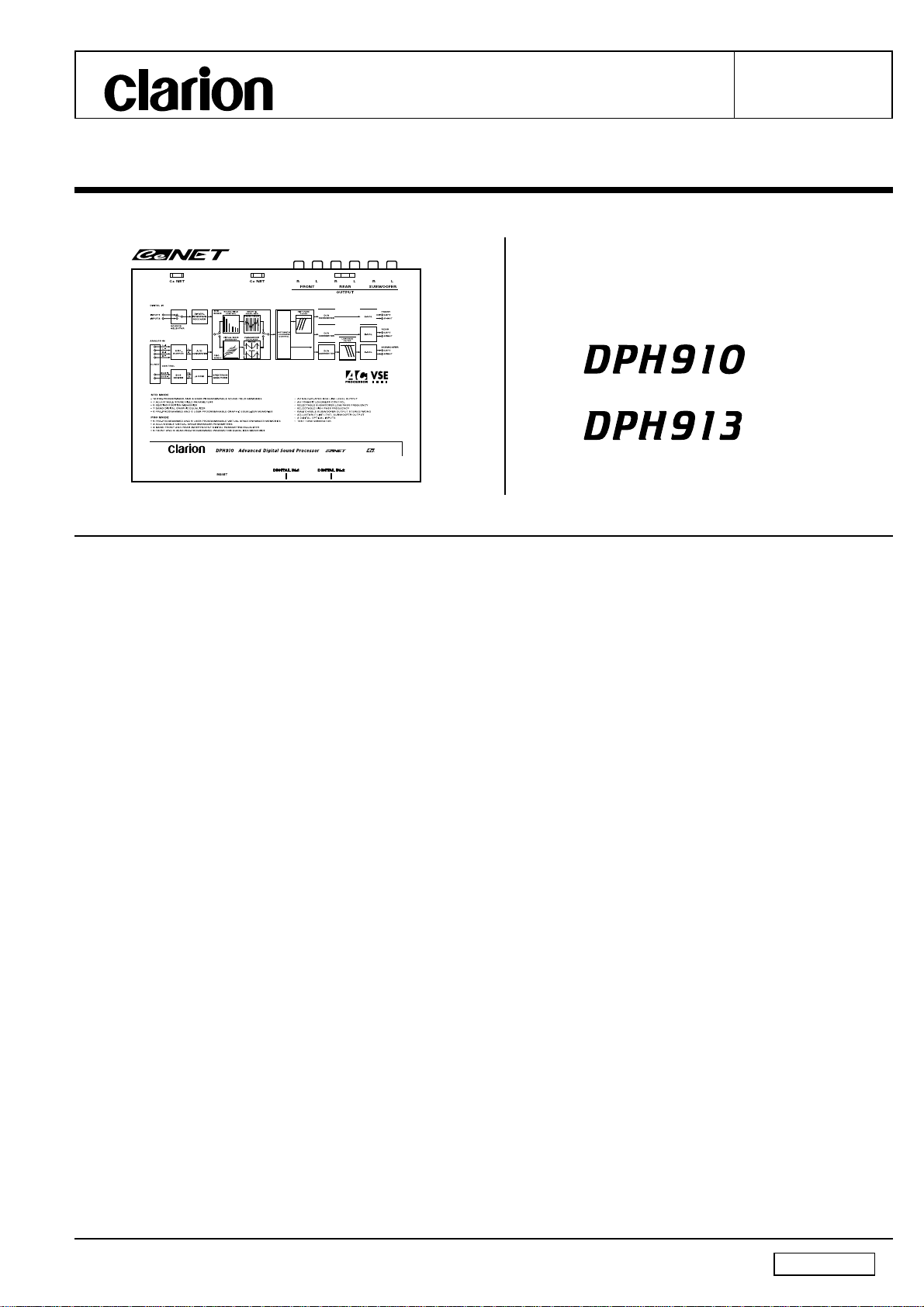
DIGITAL GRAPHIC & PARAMETRIC EQUALIZER/DSP/CROSSOVER PROCESSOR MODULE
Model
(GP-976B / FOR U.S.A.)
Model
(GP-976E / FOR EUROPE)
Published by Service Dept.
298-5921-00
Printed in Japan
Jul.2001 P
■SPECIFICATIONS
S/N retio: 107dB(digital input)
83dB(analogue input)
Frequency response: 10Hz to 20kHz(
Separation: 100dB(digital input)
80dB(analogue input)
Harmonic distortion: 0.006%(digital input,1kHz)
0.006%(analogue input,1kHz)
Voltage gain: 2.5dB(volume max. 4V pre-out)
Analogue input: 1.5VRMS(max.)
Digital input: 44.1kHz sampling frequency,
16-bit digital audio data
A/D conversion: 20-bit linear, 64 times oversamping
D/A conversion: 24-bit linear, 128 times oversamping
DSF: BASIC 12 modes
USER 6 modes
Graphic Eq.(7bands): BASIC 6 modes
USER 6 modes
Virtual Space Eq.: BASIC 6 modes
USER 6 modes
Parametric Eq.: 3 bands x 2(independent front/rear)
Centre freq. 20Hz to 20kHz,
1/3 octave steps, 31 points
Q curve 1 to 20
Gain
Preset 6 types
Auto loudness: on/off
Subwoofer: Voltage gain +12dB
(max.woofer volume)
LPF fc
Through,50Hz,80Hz,120Hz
LPF Slope 24dB/oct
±1dB)
±12dB
Front/Rear: HPF fc
Through,50Hz,80Hz,120Hz
HPF Slope 18dB/oct
Power supply voltage: DC14.4V(10.8 to 15.6V)
negative ground
Power consumption: 560mA
Dimentions(mm): 230(W)x25(H)x170(D)
Weight: 0.95kg
※ Specification and design are subject to change without
notice for further improvement.
■COMPONENTS
GP-976B-51/GP-976E-51
Main unit −−−−− 1
Nameplate 287-1676-00 1
Ground lead 850-2715-00 1
CeNET cable 855-3421-00 1
RCA cable 855-8500-00 2
Parts bag
Mounting bracket 300-7362-00 2
Cord clamp 335-0833-01 2
Canoe clip 335-2515-00 4
Cable clip 335-3744-00 1
Machine screw(M4X8) 714-4008-80 4
−−−−−
■NOTE
We cannot supply PWB with component parts in principle.
When a circuit on PWB has failure , please repair it by component parts base. Parts which are not mentioned in service manual are not supplied.
- 1 -
DPH910/913
Page 2

■To engineers in charge of repair or
inspection of our products.
Before repair or inspection, make sure to follow
the instructions so that customers and Engineers
in charge of repair or inspection can avoid suffering any risk or injury.
1. Use specified parts.
The system uses parts with special safety features against
fire and voltage. Use only parts with equivalent characteristics when replacing them.
The use of unspecified parts shall be regarded as remodeling for which we shall not be liable. The onus of
product liability (PL) shall not be our responsibility in cases
where an accident or failure is as a result of unspecified
parts being used.
2. Place the parts and wiring back in their original positions
after replacement or re-wiring.
For proper circuit construction, use of insulation tubes,
bonding,gaps to PWB, etc, is involved. The wiring connection and routing to the PWB are specially planned
using clamps to keep away from heated and high voltage
parts. Ensure that they are placed back in their original
positions after repair or inspection.
If extended damage is caused due to negligence during
repair, the legal responsibility shall be with the repairing
company.
3. Check for safety after repair.
Check that the screws, parts and wires are put back securely in their original position after repair. Ensure for
safety reasons there is no possibility of secondary
ploblems around the repaired spots.
If extended damage is caused due to negligence of repair, the legal responsibility shall be with the repairing
company.
4. Caution in removal and making wiring connection to the
parts for the automobile.
Disconnect the battery terminal after turning the ignition
key off. If wrong wiring connections are made with the
battery connected, a short circuit and/or fire may occur.
If extensive damage is caused due to negligence of repair, the legal responsibility shall be with the repairing
company.
5. Cautions regarding chips.
Do not reuse removed chips even when no abnormality
is observed in their appearance. Always replace them
with new ones. (The chip parts include resistors, capacitors, diodes, transistors, etc). The negative pole of tantalum capacitors is highly susceptible to heat, so use special care when replacing them and check the operation
afterwards.
6. Cautions in handling flexible PWB
Before working with a soldering iron, make sure that the
iron tip temperature is around 270
apply the iron tip repeatedly(more than three times)to the
same patterns. Also take care not to apply the tip with
force.
7. Turn the unit OFF during disassembly and parts replacement. Recheck all work before you apply power to the
unit.
℃. Take care not to
■RESET SWITCH
When no sound is heard,press this switch.
Pressinng the reset switch performs the system check.
DPH910/913
- 2 -
Page 3
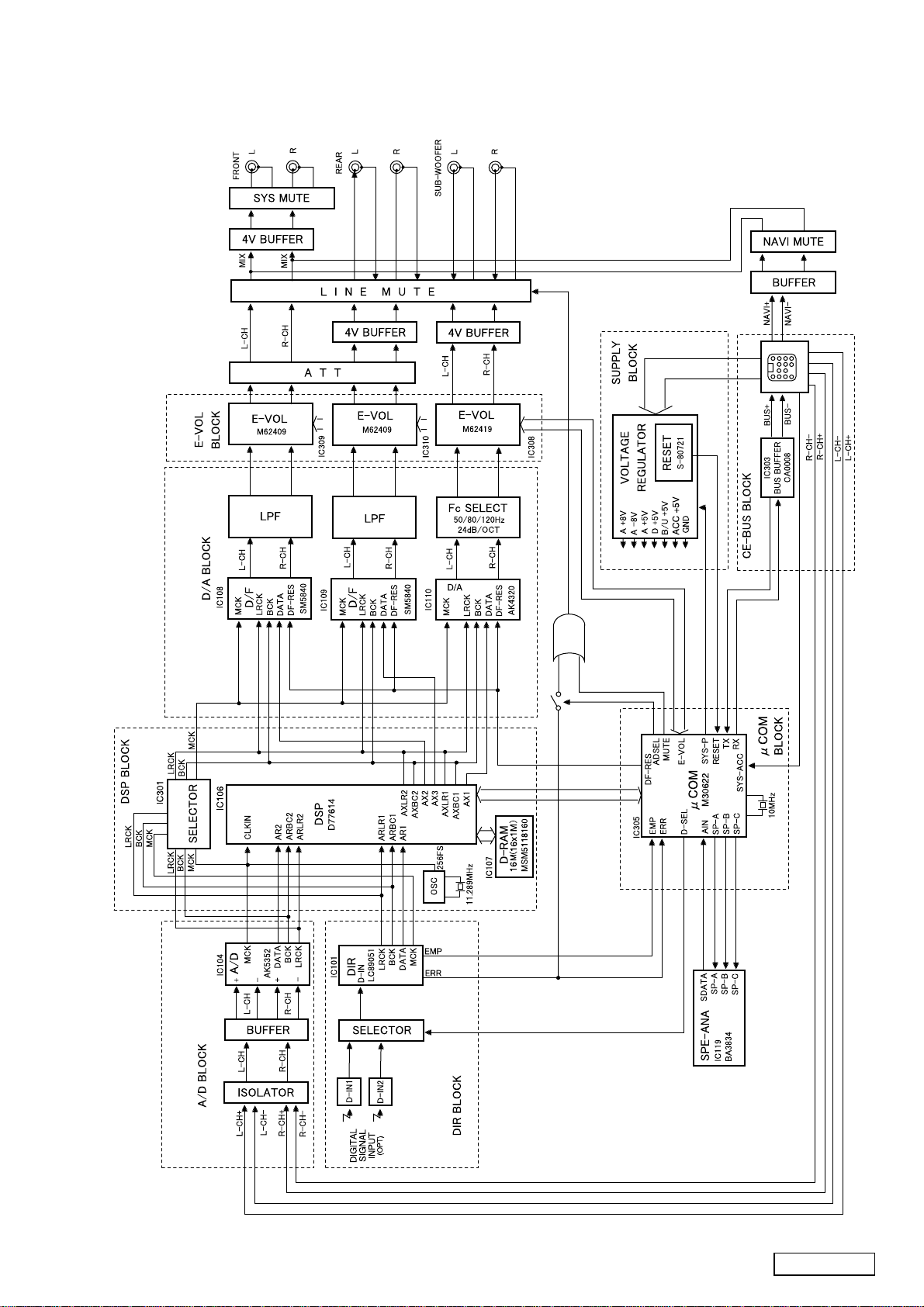
■BLOCK DIAGRAM
- 3 -
DPH910/913
Page 4

■EXPLANATION OF IC
052-7058-00 M30622MCA-E70FP DSP System Controller
1.Terminal Description
pin 1: NU : - : Not in use.
pin 2: D SEL 1 : O : Digital input selection.
pin 3: D SEL 2 : O : Digital input selection.
pin 4: D OFF : O : Digital input OFF = "H".
pin 5: EMPH : IN : The emphasis flag input.
pin 6: DIR ERR : IN: The digital-audio-interface-receiver error de-
tection flag input.
pin 7: NU : - : Not in use.
pin 8: BYTE : IN : The data length selection(8bit/16bit).
pin 9: CN VSS : IN : Inputting "L" at single mode operation.
pin 10: NU : - : Not in use.
pin 11: NU : - : Not in use.
pin 12: RESET : IN : Reset signal input.
pin 13: X OUT : O : Crystal connection.
pin 14: VSS : - : Negative supply voltage.
pin 15: X IN :IN : Crystal connection.
pin 16: VCC : - : Positive supply voltage.
pin 17: NMI :IN: Not in use.
pin 18: SYS ACC : IN : ACC detect signal input.
pin 19: B/U DET : IN : Backup voltage ON signal input.
pin 20: NU : - : Not in use.
pin 21: NU : - : Not in use.
pin 22: NU : - : Not in use.
pin 23: NU : - : Not in use.
pin 24: NU : - : Not in use.
pin 25: NU : - : Not in use.
pin 26: NU : - : Not in use.
pin 27: NU : - : Not in use.
pin 28: NU : - : Not in use.
pin 29: RX : IN : Serial data input from Ce-NET.
pin 30: TX : O : Serial data output to Ce-NET.
pin 31: Band Sel 3 : O : Spectrum analyzer band selection.
pin 32: Band Sel 2 : O : Spectrum analyzer band selection.
pin 33: Band Sel 1 : O : Spectrum analyzer band selection.
pin 34: NU : - : Not in use.
pin 35: NU : - : Not in use.
pin 36: NU : - : Not in use.
pin 37: NU : - : Not in use.
pin 38: NU : - : Not in use.
pin 39: NU : - : Not in use.
pin 40: NU : - : Not in use.
pin 41: NU : - : Not in use.
pin 42: NU : - : Not in use.
pin 43: NU : - : Not in use.
pin 44: NAVI IN : O : Navigation audio signal interrupt flag output.
pin 45: NU : - : Not in use.
pin 46: NU : - : Not in use.
pin 47 : EMPTY : IN : The acceptable flag input for the DSP data
transmission.
pin 48: NU : - : Not in use.
pin 49: HR : O : The serial data output to the DSP IC.
pin 50: HR BCK : O : The bit clock output to the DSP IC.
pin 51: HRS : O : The shift clock output to the DSP IC.
pin 52: D CS : O : The chip selection signal output to the DSP
IC.
pin 53: D RESET : O : The reset pulse output to the DSP IC.
pin 54: D MUTE : O : The mute command output to the DSP IC.
pin 55: SYS MUTE : O : System mute signal output.
pin 56: ATT : O : Attenuation command output.
pin 57: LINE MUTE : O : Audio mute signal output.
pin 58: AD SEL : O : Input selection. Analog/Digital.
pin 59: DF RES : O : Reset pulse output to ADC-IC and DF-IC.
pin 60: NU : - : Not in use.
pin 61: NU : - : Not in use.
pin 62: VCC : - : Positive supply voltage.
pin 63: NU : - : Not in use.
pin 64: VSS : - : Negative supply voltage.
pin 65: NU : - : Not in use.
pin 66: NU : - : Not in use.
pin 67: NU : - : Not in use.
pin 68: VOL S : O : Serial data output to the electric volume IC.
pin 69: VOL CKS : O : Clock pulse output to the electric volume IC.
pin 70: VOL F : O : Serial data output to the electric volume IC.
pin 71: VOL CLOCK : O : Clock pulse output to the electric volume IC.
pin 72: VOL STB : O : Strobe pulse output to the Electric volume
pin 73: NU : - : Not in use.
pin 74: NU : - : Not in use.
pin 75: NU : - : Not in use.
pin 76: NU : - : Not in use.
pin 77: NU : - : Not in use.
pin 78: NU : - : Not in use.
pin 79: NU : - : Not in use.
pin 80: NU : - : Not in use.
pin 81: NU : - : Not in use.
pin 82: NU : - : Not in use.
pin 83: SYS P 1 : O : Power supply control signal output.
pin 84: SYS P 2 : O : Power supply control signal output.
pin 85: NU : - : Not in use.
pin 86: NU : - : Not in use.
pin 87: NU : - : Not in use.
pin 88: NU : - : Not in use.
pin 89: NU : - : Not in use.
pin 90: NU : - : Not in use.
pin 91: NU : - : Not in use.
pin 92: NU : - : Not in use.
pin 93: NU : - : Not in use.
pin 94: SPD : O : Spectrum analyzer data output.
pin 95: NU : - : Not in use.
pin 96: A VSS : - : Analog ground.
pin 97: NU : - : Not in use.
pin 98: Vref : - : Reference voltage
pin 99: A VCC : - : Positive supply voltage for the internal an-
pin100: NU : - : Not in use.
(for the sub woofer)
(for the sub woofer)
(for the front signal & the rear signal)
(for the front signal & the rear signal)
or the digital-audio-interface-receiver.
alog section.
DPH910/913
- 4 -
Page 5

■EXPLOODED VIEW・PARTS LIST
Note)Some parts depend on each model.
The model name is specified in the description.
NO. PART NO. DESCRIPTION Q'TYNO. PART NO. DESCRIPTION Q'TY
1 286-9540-00 SETPLATE(GP-976B) 1
2 310-1642-04 UPPER CASE(GP-976B) 1
3 311-1731-00 LOWER CASE 1
4 347-3819-00 SPACER 1
5 731-2606-81 TAPTIGHT(M2.6x6) 3
6 731-3006-80 TAPTIGHT(M3x6) 8
7 039-1916-00 MAIN PWB 1
8 013-3932-00 SWITCH 1
9 073-0731-01 TERMINAL 2
10 074-1163-03 OUTLET SOCKET(3P) 1
286-9566-01 SETPLATE(GP-976E)
310-1642-06 UPPER CASE(GP-976E)
(WITHOUT COMPONENT)
11 074-1163-11 OUTLET SOCKET(11P) 1
12 074-1194-00 OUTLET SOCKET(CeNET) 2
13 854-9903-00 EXTENSION LEAD 1
14 075-0305-01 JACK(DIGITAL IN) 2
15 075-0336-00 JACK(RCA) 3
16 076-0543-03 PLUG(3P) 1
17 076-0543-11 PLUG(11P) 1
18 103-1266-00 TRANSISTOR(2SD1266) 1
19 331-0162-00 JACK HOLDER 1
20 331-0278-00 CONNECTOR HOLDER 2
21 331-2302-00 CONNECTOR HOLDER 2
■ELECTRICAL PARTS LIST
Main PWB section(B1)
REF No. PART No. DESCRIPTION REF No. PART No. DESCRIPTION REF No. PART No. DESCRIPTION
C101 166-2201-50 22pF CH
C102 168-1032-55 0.01μF
C103 182-1043-69 50V0.1μF
C104 182-4763-29 10V47μF
C105 168-1045-56 0.1μF
C106 182-4763-19 6.3V47μF
C107 168-1045-56 0.1μF
C109 043-0264-58 1500pF
C110 043-0264-58 1500pF
C111 182-1063-35 16V10μF
C112 182-4763-19 6.3V47μF
C113 168-1045-56 0.1μF
C114 168-1045-56 0.1μF
C115 168-1045-56 0.1μF
Note)Several different parts of the same reference number are alternative parts.
One of those parts is used in the set.
C116 182-1063-39 16V10μF
C118 166-1201-50 12pF CH
C119 168-1045-56 0.1μF
C121 166-1201-50 12pF CH
C123 168-1045-56 0.1μF
C124 182-4763-19 6.3V47μF
C128 168-1045-56 0.1μF
C129 182-1073-39 16V100μF
C134 182-1063-39 16V10μF
C135 168-1045-56 0.1μF
C136 182-1063-35 16V10μF
C137 168-1045-56 0.1μF
C138 182-1063-35 16V10μF
C139 168-1022-55 1000pF
C140 168-1022-55 1000pF
C141 168-1022-55 1000pF
C151 168-1045-56 0.1μF
C152 182-1063-35 16V10μF
C153 168-1045-56 0.1μF
C154 168-1045-56 0.1μF
C155 182-1063-35 16V10μF
C156 168-1045-56 0.1μF
C157 042-0554-66 16V10μF
C158 042-0554-66 16V10μF
C159 168-1045-56 0.1μF
C160 042-0554-66 16V10μF
C161 168-1045-56 0.1μF
C162 182-1063-35 16V10μF
- 5 -
DPH910/913
Page 6

REF No. PART No. DESCRIPTION REF No. PART No. DESCRIPTION REF No. PART No. DESCRIPTION
C163 182-1063-35 16V10μF
C164 182-1063-35 16V10μF
C165 182-1063-35 16V10μF
C166 043-0264-63 0.01μF
C167 043-0264-63 0.01μF
C168 168-1045-56 0.1μF
C169 182-4763-19 6.3V47μF
C170 166-5611-50 560pF CH
C171 166-5611-50 560pF CH
C172 043-0264-63 0.01μF
C173 043-0264-63 0.01μF
C174 166-5611-50 560pF CH
C175 166-5611-50 560pF CH
C177 182-1063-35 16V10μF
C178 168-1045-56 0.1μF
C179 042-0554-66 16V10μF
C180 042-0554-66 16V10μF
C181 168-1045-56 0.1μF
C182 042-0554-66 16V10μF
C183 168-1045-56 0.1μF
C184 182-1063-35 16V10μF
C185 182-1063-35 16V10μF
C186 182-1063-35 16V10μF
C187 182-1063-35 16V10μF
C188 043-0264-63 0.01μF
C189 043-0264-63 0.01μF
C190 166-5611-50 560pF CH
C191 166-5611-50 560pF CH
C192 043-0264-63 0.01μF
C193 043-0264-63 0.01μF
C194 168-1045-56 0.1μF
C195 182-4763-19 6.3V47μF
C196 166-5611-50 560pF CH
C197 166-5611-50 560pF CH
C199 182-1063-35 16V10μF
C201 182-1063-39 16V10μF
C202 182-1063-39 16V10μF
C205 182-1043-65 50V0.1μF
C206 182-1043-65 50V0.1μF
C207 168-1045-56 0.1μF
C208 168-1045-56 0.1μF
C209 168-1022-55 1000pF
C210 182-1053-65 50V1μF
C211 182-1053-65 50V1μF
C212 182-1053-65 50V1μF
C213 182-1053-65 50V1μF
C214 182-1063-35 16V10μF
C215 182-1063-35 16V10μF
C216 168-1045-56 0.1μF
C217 168-1045-56 0.1μF
C218 168-1045-56 0.1μF
C219 168-1045-56 0.1μF
C221 168-3312-55 330pF
C222 166-2701-50 27pF CH
C223 166-2701-50 27pF CH
C224 166-2701-50 27pF CH
C225 166-2701-50 27pF CH
C226 166-2701-50 27pF CH
C227 166-2701-50 27pF CH
C228 166-2701-50 27pF CH
C229 166-2701-50 27pF CH
C230 168-1032-55 0.01μF
C231 168-1032-55 0.01μF
C232 168-1032-55 0.01μF
C233 166-1011-50 100pF CH
C301 168-1045-56 0.1μF
C302 168-1045-56 0.1μF
C305 184-2283-31 16V 2200μF
C306 182-3353-65 50V3.3μF
C307 182-3353-65 50V3.3μF
C308 182-3353-65 50V3.3μF
C309 182-3353-65 50V3.3μF
C310 182-4753-59 35V4.7μF
C311 182-1063-39 16V10μF
C312 182-1073-35 16V100μF
C313 182-1063-39 16V10μF
C314 168-1045-56 0.1μF
C316 168-1045-56 0.1μF
C317 182-1063-39 16V10μF
C318 184-2273-19 6.3V220μF
C319 168-1045-56 0.1μF
C320 168-1045-56 0.1μF
C321 168-3332-78 0.033μF
C322 182-1063-35 16V10μF
C324 168-1022-55 1000pF
C325 184-2273-29 10V220μF
C326 182-1063-39 16V10μF
C327 184-2273-19 6.3V220μF
C328 168-1045-56 0.1μF
C329 168-1045-56 0.1μF
C330 182-1063-39 16V10μF
C331 168-2232-55 0.022μF
C332 182-2263-35 16V22μF
C333 168-2232-55 0.022μF
C334 182-2263-35 16V22μF
C335 168-1045-56 0.1μF
C336 184-3373-29 10V330μF
C337 166-2211-50 220pF CH
C338 168-1045-56 0.1μF
C341 182-1073-35 16V100μF
C342 168-1045-56 0.1μF
C343 168-1022-55 1000pF
C344 168-2232-55 0.022μF
C345 182-1063-35 16V10μF
C346 168-2232-55 0.022μF
C347 182-2263-35 16V22μF
C348 168-1045-56 0.1μF
C349 168-1022-55 1000pF
C350 182-4763-25 10V47μF
C351 043-0311-92 10V0.22μF
C352 042-0554-66 16V10μF
C353 168-1022-55 1000pF
C354 182-4763-25 10V47μF
C355 043-0311-92 10V0.22μF
C356 042-0554-66 16V10μF
C357 168-1045-56 0.1μF
C358 182-1063-35 16V10μF
C359 182-1063-35 16V10μF
C360 042-0554-57 6.3V47μF
C361 182-1063-35 16V10μF
C362 182-1063-35 16V10μF
C363 042-0554-57 6.3V47μF
C364 182-1063-35 16V10μF
C365 168-1022-55 1000pF
C366 168-1022-55 1000pF
C367 043-0311-92 10V0.22μF
C368 043-0311-92 10V0.22μF
C369 182-2253-65 50V2.2μF
C370 182-2253-65 50V2.2μF
C371 182-1063-35 16V10μF
C372 182-1063-35 16V10μF
C373 168-1032-55 0.01μF
C374 168-1032-55 0.01μF
C375 168-1032-55 0.01μF
C376 168-1032-55 0.01μF
C377 168-1032-55 0.01μF
C378 168-1032-55 0.01μF
C379 182-3353-65 50V3.3μF
C380 182-3353-65 50V3.3μF
C381 182-3353-65 50V3.3μF
C382 182-3353-65 50V3.3μF
C383 182-4753-55 35V4.7μF
C384 182-4753-55 35V4.7μF
C385 168-1045-56 0.1μF
C386 168-1045-56 0.1μF
C387 172-4741-15 0.47μF
C390 168-1022-55 1000pF
C391 182-1063-35 16V10μF
C392 182-1063-35 16V10μF
C394 168-3332-78 0.033μF
C395 168-3332-78 0.033μF
C396 168-3332-78 0.033μF
C397 168-3332-78 0.033μF
C398 168-3332-78 0.033μF
C399 168-3332-78 0.033μF
C401 182-1063-35 16V10μF
C402 182-1063-35 16V10μF
C403 182-1063-35 16V10μF
C404 182-1063-35 16V10μF
C405 168-1045-56 0.1μF
C406 168-1045-56 0.1μF
C407 168-1045-56 0.1μF
C408 182-1063-35 16V10μF
C409 182-1063-35 16V10μF
C410 182-1063-35 16V10μF
C411 182-1063-35 16V10μF
C412 168-1045-56 0.1μF
C418 182-1063-35 16V10μF
C419 182-1063-35 16V10μF
C420 182-1063-35 16V10μF
C421 182-1063-35 16V10μF
C422 182-1063-35 16V10μF
C423 182-1063-35 16V10μF
C425 182-1063-39 16V10μF
C426 182-1063-39 16V10μF
C427 182-1063-35 16V10μF
C428 168-1045-56 0.1μF
C430 042-0554-66 16V10μF
C431 042-0554-66 16V10μF
C432 042-0554-66 16V10μF
C433 042-0554-66 16V10μF
C434 182-1063-35 16V10μF
C435 182-1063-35 16V10μF
C436 043-0264-56 270pF
C437 043-0264-56 270pF
C438 043-0264-56 270pF
C439 043-0264-56 270pF
C440 043-0264-56 270pF
C441 043-0264-56 270pF
C442 166-2701-50 27pF CH
C443 166-2701-50 27pF CH
C444 166-2701-50 27pF CH
C445 166-2701-50 27pF CH
C446 166-2701-50 27pF CH
C447 166-2701-50 27pF CH
C448 168-1022-55 1000pF
C449 172-4741-15 0.47μF
C454 042-0559-00 5.5V 0.1F
C455 168-1045-56 0.1μF
C456 182-4763-29 10V47μF
C457 168-1045-56 0.1μF
C462 182-3353-65 50V3.3μF
C463 182-3353-65 50V3.3μF
C464 168-1045-56 0.1μF
C471 168-1045-56 0.1μF
C472 172-3341-15 0.33μF
D101 001-0516-90 MA111
D101 001-0517-90 1SS355
D101 001-0580-90 1SS352
D301 001-0516-90 MA111
D301 001-0517-90 1SS355
D301 001-0580-90 1SS352
D302 001-0516-90 MA111
D302 001-0517-90 1SS355
D302 001-0580-90 1SS352
D303 001-0516-90 MA111
D303 001-0517-90 1SS355
D303 001-0580-90 1SS352
D304 001-0516-90 MA111
D304 001-0517-90 1SS355
D304 001-0580-90 1SS352
D310 001-0330-90 2SS119
DPH910/913
- 6 -
Page 7

REF No. PART No. DESCRIPTION REF No. PART No. DESCRIPTION REF No. PART No. DESCRIPTION
D310 001-0294-90 1SS133T
D311 001-0504-36 HZS7A1L
D312 001-0347-32 MA4056MTA
D312 001-0346-32 MTZJ5.6B
D312 001-0401-32 HZS6B1-TJ
D313 001-0529-69 MA8180-M
D313 001-0575-69 DTZ18B
D315 001-0529-69 MA8180-M
D315 001-0575-69 DTZ18B
D316 001-0504-32 HZS6A3L
D317 001-0501-90 DINS4
D317 001-0502-92 1FWJ43
D318 001-0516-90 MA111
D318 001-0517-90 1SS355
D318 001-0580-90 1SS352
D330 001-0516-90 MA111
D330 001-0517-90 1SS355
D330 001-0580-90 1SS352
D331 001-0516-90 MA111
D331 001-0517-90 1SS355
D331 001-0580-90 1SS352
D332 001-0330-90 2SS119
D332 001-0294-90 1SS133T
FIL101 060-3102-91 NFM51R00P206
FIL102 060-3102-91 NFM51R00P206
FIL302 060-3104-90 NFM41P11C204
FIL303 060-3113-95 NFM2012R13C102R
IC101 051-6327-08 LC89051VD
IC102 051-0350-93 NJM4558M
IC103 051-0350-93 NJM4558M
IC104 051-6323-28 AK5352VF
IC105 051-1443-09 TC7WU04F
IC106 051-6331-00 D77614FT
IC107 051-9308-10 HM5118160CTT-6
IC107 051-9308-31 GM71C18160CT-6
IC108 051-6371-08 VSOP20
IC109 051-6371-08 VSOP20
IC110 051-6370-08 AK4380VT
IC111 051-3015-90 NJM4580M
IC112 051-3015-90 NJM4580M
IC113 051-1378-08 TC7S04F
IC117 051-0350-93 NJM4558M
IC118 051-0350-93 NJM4558M
IC119 051-5818-90 BA3834F
IC120 051-7233-08 TC7W74F
IC121 051-7212-08 TC74HC157AF
IC301 051-1124-08 TC74HC153AF
IC303 051-6600-38 CA0008AM
IC304 051-0869-58 NJM2103M
IC305 052-7058-00 M30622MCA-E70FP
IC306 051-3605-90 NJM2360AM
IC308 051-5008-90 M62419FP
IC309 051-5003-90 M62409FP
IC310 051-5003-90 M62409FP
IC311 051-3015-90 NJM4580M
IC312 051-3015-90 NJM4580M
IC313 051-0350-93 NJM4558M
IC315 051-3236-90 BA08FP
IC316 051-0350-93 NJM4558M
IC318 051-0350-93 NJM4558M
IC319 051-5407-08 S-80721AN-DJ
IC320 051-7202-08 TC7S32F
J302 075-0336-00 2P RCA
J303 075-0336-00 2P RCA
J304 075-0336-00 2P RCA
L101 010-2285-61 BLM21P300
L102 010-2285-61 BLM21P300
L104 010-2285-58 BLM21A102FPB
L105 010-2285-58 BLM21A102FPB
L106 010-2285-58 BLM21A102FPB
L107 010-2285-58 BLM21A102FPB
L114 010-2285-58 BLM21A102FPB
L115 010-2285-58 BLM21A102FPB
L116 010-2285-58 BLM21A102FPB
L117 010-2285-58 BLM21A102FPB
L118 010-2285-58 BLM21A102FPB
L119 010-2285-58 BLM21A102FPB
L120 010-2285-58 BLM21A102FPB
L131 010-2285-56 BLM21B222S
L301 010-6009-80 47μH
L302 010-6009-80 47μH
L304 010-6009-76 22μH
L305 010-6009-73 12μH
L306 010-2200-02 270μH
L307 010-6009-73 12μH
L308 010-6009-76 22μH
L322 010-2285-58 BLM21A102FPB
L324 010-2285-58 BLM21A102FPB
L325 010-2285-58 BLM21A102FPB
L327 010-2285-58 BLM21A102FPB
L328 010-2285-58 BLM21A102FPB
L330 010-2285-58 BLM21A102FPB
L332 009-0470-05 CHOKE
L501 010-2285-56 BLM21B222S
L502 010-2285-56 BLM21B222S
L503 010-2285-56 BLM21B222S
L504 010-2285-56 BLM21B222S
L505 010-2285-56 BLM21B222S
L506 010-2285-56 BLM21B222S
L507 010-2285-56 BLM21B222S
L508 010-2285-56 BLM21B222S
L509 010-2285-56 BLM21B222S
P301 075-0305-01 OPT-DIGITAL
P302 075-0305-01 OPT-DIGITAL
P310 076-0543-11 11P
P311 076-0543-03 3P
P501 074-1163-11 11P
P502 074-1194-00 13P DIN
P505 074-1194-00 13P DIN
P507 074-1163-03 3P
Q301 191-1240-00 2SB1240
Q302 125-2031-92 MUN2211
Q302 125-2004-92 RN1402
Q305 193-1858-00 2SD1858
Q306 103-1266-00 2SD1266
Q307 190-1037-00 2SA1037
Q307 190-1162-00 2SA1162
Q308 125-2031-92 MUN2211
Q308 125-2004-92 RN1402
Q310 125-2031-92 MUN2211
Q310 125-2004-92 RN1402
Q311 193-1858-00 2SD1858
Q312 190-1037-00 2SA1037
Q312 190-1162-00 2SA1162
Q313 125-2031-92 MUN2211
Q313 125-2004-92 RN1402
Q314 125-2031-92 MUN2211
Q314 125-2004-92 RN1402
Q315 125-2031-92 MUN2211
Q315 125-2004-92 RN1402
Q316 190-1037-00 2SA1037
Q316 190-1162-00 2SA1162
Q317 125-4001-90 XN1504
Q318 125-4001-90 XN1504
Q319 125-0002-95 RN2405
Q319 125-0014-95 DTA123JK
Q320 125-2031-92 MUN2211
Q320 125-2004-92 RN1402
Q321 193-1306-00 2SD1306
Q321 192-3326-00 2SC3326
Q322 193-1306-00 2SD1306
Q322 192-3326-00 2SC3326
Q323 193-1306-00 2SD1306
Q323 192-3326-00 2SC3326
Q324 193-1306-00 2SD1306
Q324 192-3326-00 2SC3326
Q325 193-1306-00 2SD1306
Q325 192-3326-00 2SC3326
Q326 193-1306-00 2SD1306
Q326 192-3326-00 2SC3326
Q327 125-0002-93 RN2403
Q327 125-0001-92 UN2112
Q328 125-2031-92 MUN2211
Q328 125-2004-92 RN1402
Q329 125-4001-90 XN1504
Q330 190-1037-00 2SA1037
Q330 190-1162-00 2SA1162
Q331 125-2031-92 MUN2211
Q331 125-2004-92 RN1402
Q332 125-2031-92 MUN2211
Q332 125-2004-92 RN1402
Q442 193-1306-00 2SD1306
Q442 192-3326-00 2SC3326
Q443 125-0002-95 RN2405
Q443 125-0014-95 DTA123JK
Q444 125-0002-95 RN2405
Q444 125-0014-95 DTA123JK
Q445 125-0002-95 RN2405
Q445 125-0014-95 DTA123JK
Q446 125-0002-95 RN2405
Q446 125-0014-95 DTA123JK
Q447 125-0002-95 RN2405
Q447 125-0014-95 DTA123JK
Q448 125-0002-95 RN2405
Q448 125-0014-95 DTA123JK
Q449 125-0002-95 RN2405
Q449 125-0014-95 DTA123JK
Q450 125-0002-95 RN2405
Q450 125-0014-95 DTA123JK
Q451 125-0002-95 RN2405
Q451 125-0014-95 DTA123JK
Q452 125-0002-95 RN2405
Q452 125-0014-95 DTA123JK
Q453 125-0002-95 RN2405
Q453 125-0014-95 DTA123JK
Q454 125-0002-95 RN2405
Q454 125-0014-95 DTA123JK
Q455 125-0002-95 RN2405
Q455 125-0014-95 DTA123JK
R101 119-2231-15 1/16W 22kΩ
R102 119-1011-15 1/16W 100Ω
R103 119-5121-15 1/16W 5.1kΩ
R104 119-2431-15 1/16W 24kΩ
R105 032-0140-89 1/4W 47kΩ±1%
R106 032-0140-89 1/4W 47kΩ±1%
R107 032-0140-89 1/4W 47kΩ±1%
R108 032-0140-89 1/4W 47kΩ±1%
R109 032-0140-69 1/4W 16kΩ±1%
R110 032-0140-69 1/4W 16kΩ±1%
R111 032-0140-69 1/4W 16kΩ±1%
R112 032-0140-69 1/4W 16kΩ±1%
R113 119-2421-15 1/16W 2.4kΩ
R114 119-1511-15 1/16W 150Ω
R115 119-1031-15 1/16W 10kΩ
R117 119-1031-15 1/16W 10kΩ
R119 119-1031-15 1/16W 10kΩ
R120 119-1031-15 1/16W 10kΩ
R121 119-2711-15 1/16W 270Ω
R122 119-2711-15 1/16W 270Ω
R123 119-2711-15 1/16W 270Ω
R124 119-3311-15 1/16W 330Ω
R125 119-3311-15 1/16W 330Ω
R126 119-3311-15 1/16W 330Ω
R127 119-3311-15 1/16W 330Ω
R129 119-2711-15 1/16W 270Ω
R130 119-2711-15 1/16W 270Ω
R131 119-2711-15 1/16W 270Ω
R132 119-1051-15 1/16W 1MΩ
R136 119-2711-15 1/16W 270Ω
R137 119-2711-15 1/16W 270Ω
R138 119-2711-15 1/16W 270Ω
R141 119-4731-15 1/16W 47kΩ
- 7 -
DPH910/913
Page 8

REF No. PART No. DESCRIPTION REF No. PART No. DESCRIPTION REF No. PART No. DESCRIPTION
R143 119-4731-15 1/16W 47kΩ
R152 119-4721-15 1/16W 4.7kΩ
R161 119-5121-15 1/16W 5.1kΩ
R165 119-4731-15 1/16W 47kΩ
R166 119-4731-15 1/16W 47kΩ
R167 119-1051-15 1/16W 1MΩ
R168 119-0000-05 1/16W 0Ω JW
R170 032-0140-50 1/16W 10kΩ±1%
R171 032-0140-50 1/16W 10kΩ±1%
R172 032-0140-50 1/16W 10kΩ±1%
R173 032-0140-98 1/16W 120kΩ±1%
R174 032-0140-98 1/16W 120kΩ±1%
R175 032-0140-50 1/16W 10kΩ±1%
R176 032-0140-50 1/16W 10kΩ±1%
R177 032-0140-50 1/16W 10kΩ±1%
R178 119-8221-15 1/16W 8.2kΩ
R179 032-0140-50 1/16W 10kΩ±1%
R180 032-0140-50 1/16W 10kΩ±1%
R181 032-0140-98 1/16W 120kΩ±1%
R182 032-0140-98 1/16W 120kΩ±1%
R183 119-1031-15 1/16W 10kΩ
R184 119-4731-15 1/16W 47kΩ
R185 119-4731-15 1/16W 47kΩ
R186 032-0140-50 1/16W 10kΩ±1%
R187 032-0140-50 1/16W 10kΩ±1%
R188 032-0140-50 1/16W 10kΩ±1%
R189 119-1021-15 1/16W 1kΩ
R190 119-1021-15 1/16W 1kΩ
R191 032-0140-50 1/16W 10kΩ±1%
R192 032-0140-50 1/16W 10kΩ±1%
R193 032-0140-98 1/16W 120kΩ±1%
R194 032-0140-98 1/16W 120kΩ±1%
R195 032-0140-50 1/16W 10kΩ±1%
R196 119-3901-15 1/16W 390Ω
R197 032-0140-50 1/16W 10kΩ±1%
R198 032-0140-50 1/16W 10kΩ±1%
R199 032-0140-98 1/16W 120kΩ±1%
R200 032-0140-98 1/16W 120kΩ±1%
R201 119-2711-15 1/16W 270Ω
R210 119-1041-15 1/16W 100kΩ
R211 119-1041-15 1/16W 100kΩ
R212 119-1541-15 1/16W 150kΩ
R213 119-1541-15 1/16W 150kΩ
R214 119-1221-15 1/16W 1.2kΩ
R216 119-2711-15 1/16W 270Ω
R217 119-2711-15 1/16W 270Ω
R218 119-2711-15 1/16W 270Ω
R219 119-2711-15 1/16W 270Ω
R220 119-1041-15 1/16W 100kΩ
R221 119-1031-15 1/16W 10kΩ
R222 119-1031-15 1/16W 10kΩ
R224 119-1021-15 1/16W 1kΩ
R305 119-2231-15 1/16W 22kΩ
R306 111-1521-94 1/4WS 1.5kΩ
R308 119-8211-15 1/16W 820Ω
R309 119-8211-15 1/16W 820Ω
R311 119-1821-15 1/16W 1.8kΩ
R313 119-4701-15 1/16W 47Ω
R314 119-4701-15 1/16W 47Ω
R318 119-1821-15 1/16W 1.8kΩ
R319 119-1031-15 1/16W 10kΩ
R321 111-4711-94 1/4WS 470Ω
R323 119-2231-15 1/16W 22kΩ
R324 119-2231-15 1/16W 22kΩ
R326 119-2731-15 1/16W 27kΩ
R327 119-1031-15 1/16W 10kΩ
R328 119-1541-15 1/16W 150kΩ
R331 119-1031-15 1/16W 10kΩ
R332 119-4711-15 1/16W 470Ω
R333 119-1831-15 1/16W 18kΩ
R334 119-1031-15 1/16W 10kΩ
R335 119-3321-15 1/16W 3.3kΩ
R336 119-1031-15 1/16W 10kΩ
R337 111-2791-94 1/4WS 2.7Ω
R338 111-2791-94 1/4WS 2.7Ω
R339 119-1031-15 1/16W 10kΩ
R340 119-2041-15 1/16W 200kΩ
R341 119-2041-15 1/16W 200kΩ
R342 119-2041-15 1/16W 200kΩ
R343 119-2041-15 1/16W 200kΩ
R345 119-4731-15 1/16W 47kΩ
R346 119-6831-15 1/16W 68kΩ
R347 119-1241-15 1/16W 120kΩ
R348 119-1241-15 1/16W 120kΩ
R349 119-6831-15 1/16W 68kΩ
R350 119-4731-15 1/16W 47kΩ
R351 119-1841-15 1/16W 180kΩ
R352 119-1841-15 1/16W 180kΩ
R353 119-1041-15 1/16W 100kΩ
R354 119-1041-15 1/16W 100kΩ
R355 119-6831-15 1/16W 68kΩ
R356 119-6831-15 1/16W 68kΩ
R357 119-1021-15 1/16W 1kΩ
R358 119-1041-15 1/16W 100kΩ
R359 119-1241-15 1/16W 120kΩ
R362 119-1241-15 1/16W 120kΩ
R363 119-6831-15 1/16W 68kΩ
R366 119-6831-15 1/16W 68kΩ
R367 119-4731-15 1/16W 47kΩ
R368 119-2221-15 1/16W 2.2kΩ
R369 119-4731-15 1/16W 47kΩ
R372 119-4731-15 1/16W 47kΩ
R373 119-1011-15 1/16W 100Ω
R374 119-1021-15 1/16W 1kΩ
R375 119-1021-15 1/16W 1kΩ
R376 119-1021-15 1/16W 1kΩ
R377 119-1021-15 1/16W 1kΩ
R378 119-1031-15 1/16W 10kΩ
R379 119-1031-15 1/16W 10kΩ
R380 119-1031-15 1/16W 10kΩ
R381 119-1031-15 1/16W 10kΩ
R382 119-1021-15 1/16W 1kΩ
R383 119-9111-15 1/16W 910Ω
R384 119-9111-15 1/16W 910Ω
R385 119-9111-15 1/16W 910Ω
R386 119-9111-15 1/16W 910Ω
R389 119-1231-15 1/16W 12kΩ
R390 119-1231-15 1/16W 12kΩ
R391 032-0144-53 1/10W 10kΩ
R392 032-0144-53 1/10W 10kΩ
R393 032-0144-53 1/10W 10kΩ
R394 032-0144-53 1/10W 10kΩ
R395 119-2731-15 1/16W 27kΩ
R396 119-2731-15 1/16W 27kΩ
R397 119-2731-15 1/16W 27kΩ
R398 119-2731-15 1/16W 27kΩ
R399 119-3031-15 1/16W 30kΩ
R400 119-3031-15 1/16W 30kΩ
R401 119-1021-15 1/16W 1kΩ
R402 119-1021-15 1/16W 1kΩ
R403 119-4731-15 1/16W 47kΩ
R404 119-1011-15 1/16W 100Ω
R405 119-2221-15 1/16W 2.2kΩ
R406 119-1041-15 1/16W 100kΩ
R407 119-3311-15 1/16W 330Ω
R408 119-1021-15 1/16W 1kΩ
R409 119-1021-15 1/16W 1kΩ
R410 119-3311-15 1/16W 330Ω
R411 119-3311-15 1/16W 330Ω
R412 119-1021-15 1/16W 1kΩ
R413 119-1021-15 1/16W 1kΩ
R414 119-3311-15 1/16W 330Ω
R415 119-3311-15 1/16W 330Ω
R416 119-1021-15 1/16W 1kΩ
R417 119-1021-15 1/16W 1kΩ
R418 119-3311-15 1/16W 330Ω
R419 119-2231-15 1/16W 22kΩ
R420 119-2231-15 1/16W 22kΩ
R421 119-2231-15 1/16W 22kΩ
R422 119-2231-15 1/16W 22kΩ
R423 119-2231-15 1/16W 22kΩ
R424 119-2231-15 1/16W 22kΩ
R425 119-4731-15 1/16W 47kΩ
R431 119-1031-15 1/16W 10kΩ
R432 119-2711-15 1/16W 270Ω
R433 119-2711-15 1/16W 270Ω
R434 119-2711-15 1/16W 270Ω
R435 119-2711-15 1/16W 270Ω
R436 119-2711-15 1/16W 270Ω
R440 119-1031-15 1/16W 10kΩ
R441 119-3321-15 1/16W 3.3kΩ
R445 032-0140-89 1/4W 47kΩ±1%
R446 032-0140-89 1/4W 47kΩ±1%
R447 032-0140-50 1/16W 10kΩ±1%
R448 032-0140-50 1/16W 10kΩ±1%
R449 119-1031-15 1/16W 10kΩ
R450 119-5621-15 1/16W 5.6kΩ
R451 119-1021-15 1/16W 1kΩ
R452 119-1031-15 1/16W 10kΩ
R453 119-5621-15 1/16W 5.6kΩ
R455 119-5631-15 1/16W 56kΩ
R456 119-5631-15 1/16W 56kΩ
R457 119-4731-15 1/16W 47kΩ
R458 119-4731-15 1/16W 47kΩ
R459 119-4731-15 1/16W 47kΩ
R462 119-4731-15 1/16W 47kΩ
S301 013-3932-00 SKHHLN
X101 061-3049-00 11.2896MH
X301 060-1505-50 10MHz
DPH910/913
- 8 -
Page 9

■ CIRCUIT DIAGRAM
Main PWB section 1/3 (B1)
- 9 -
DPH910/913
Page 10

Page 11

Page 12

 Loading...