

Page 1
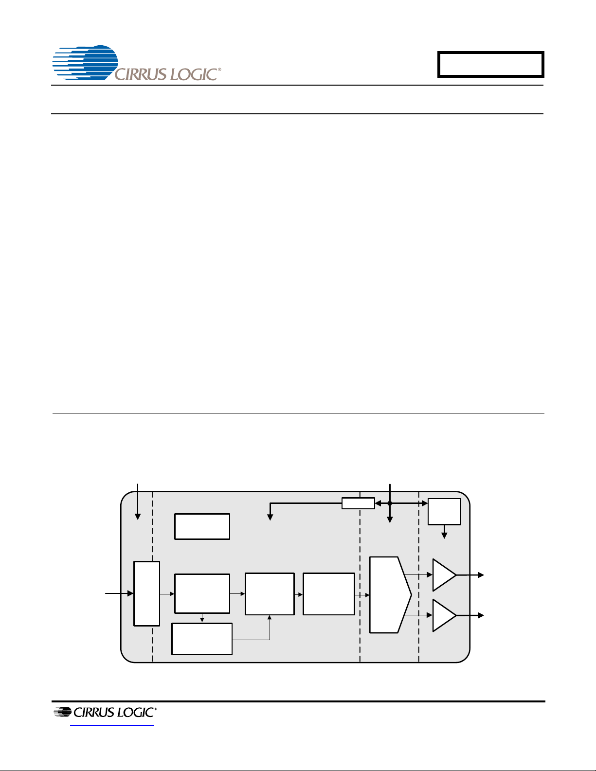
PCM Serial
Audio Port
Level Shifter
I²S Serial
Audio Input
Multibit
Modulator
Interpolation
Filters + HPF
Left Channel
Right Channel
Power-On
Reset
Auto Speed
Mode Detect
Analog Supply (VA)
+5 V
Inverting
Charge
Pump
1.8V reg
-VA
Interface Supply (VL)
+1.8V to +5V
Ground-Centered,
2 Vrms Line Level
Outputs
DAC
CS4354
5-V Stereo DAC with 2-V
Features
Advanced multibit delta–sigma modulator
101 dB A-weighted dynamic range
–86 dB THD+N
Single-ended ground-centered analog
architecture
– No DC-blocking capacitors required
– Integrated inverting charge pump
– Filtered line-level outputs
–2V
Low-latency digital filtering
Supports sample rates up to 192 kHz
24-bit I²S input
+5-V analog supply with integrated inverting
charge pump and regulator for core logic, and
+1.8-V to +5-V interface power supplies
50-mW power consumption
14-pin SOIC, lead-free assembly
full-scale output
RMS
RMS
Ground-Centered Output
Description
The CS4354 is a complete stereo digital-to-analog system including digital interpolation, third-order multi-bit
delta–sigma digital-to-analog conversion, digital de- emphasis, analog filtering, and on-chip 2 V
driver from a 5 V supply.
The advantages of this architecture include ideal differential linearity, no distortion mechanisms due to resistor
matching errors, no linearity drift over time and temperature, high tolerance to clock jitter, and a minimal set of
external components.
These features are ideal for cost-sensitive, two-channel
audio systems including video game consoles, Blu-Ray
®
Disc
and DVD players, set-top boxes, digital TVs, and
DAB/DMB devices.
The CS4354 is available in a 14-pin SOIC package in
Commercial (–40°C to +85°C) grade. The CDB4354
Customer Demonstration Board is also available for device evaluation and implementation suggestions.
Please see “Ordering Information” on page 23 for complete details.
RMS
line-level
http://www.cirrus.com
Copyright Cirrus Logic, Inc. 2011
(All Rights Reserved)
Sept '11
DS895F2
Page 2

TABLE OF CONTENTS
1. PIN DESCRIPTIONS ...................................... ... ... ... .... ... .......................................... ... ... ..................... 4
2. CHARACTERISTICS AND SPECIFICATIONS ...................................................................................... 5
RECOMMENDED OPERATING CONDITIONS .................................................................................... 5
ABSOLUTE MAXIMUM RATINGS ........................................................................................................ 5
DAC ANALOG CHARACTERISTICS .................................................................................................... 6
COMBINED DIGITAL AND ON-CHIP ANALOG FILTER CHARACTERISTICS ................................... 7
SWITCHING SPECIFICATIONS - SERIAL AUDIO INTERFACE ......................................................... 8
DIGITAL INTERFACE CHARACTERISTICS ....... ... ... .... ... ... ... .... ............................................. ... ... ... ... 10
INTERNAL POWER-ON RESET THRESHOLD VOLTAGES ............................................................. 10
DC ELECTRICAL CHARACTERISTICS .............................................................................................. 11
2.1 Digital I/O Pin Characteristics ........................................................................................................ 11
3. TYPICAL CONNECTION DIAGRAM ................................................................................................... 12
4. APPLICATIONS ................................................................................................................................... 13
4.1 Ground-Centered Line Outputs ............................ .... ... ... ... .... ............................................. ... ......... 13
4.2 Sample Rate Range/Operational Mode Detect ................. .... ......................................... .... ... ... ... ... 13
4.3 System Clocking ............................................................................................................................ 13
4.4 Serial Clock .................................................................................................................................... 14
4.4.1 External Serial Clock Mode ................................................................................................... 14
4.4.2 Internal Serial Clock Mode .................................................................................................... 14
4.4.2.1 De-Emphasis Control ................................................................................................. 14
4.5 Internal High-Pass Filter ................................................................................................................ 15
4.6 Digital Interface Format .................................................................................................................. 15
4.7 Internal Power-On Reset ............................................................................................................... 15
4.8 Initialization .................................................................................................................................... 16
4.9 Recommended Operational Sequences ........................................................................................ 18
4.9.1 Power-Up .... ... .......................................... ... .......................................... .... ... ......................... 18
4.9.2 Power-Down ................................... .... ... ... ... .... .......................................... ... ... ... ... ................ 18
4.9.3 Sample Rate Change ......... ... ... ... ... .... .......................................... ... ... ... .... ... ... ... ................... 18
4.10 Grounding and Power Supply Arrangements .............................................................................. 18
4.10.1 Capacitor Placement ........................................................................................................... 19
5. COMBINED DIGITAL AND ON-CHIP ANALOG FILTER RESPONSE PLOTS .............................. 20
6. PARAMETER DEFINITIONS ................................................................................................................ 22
7. PACKAGE INFORMATION .................................................................................................................. 23
7.1 Dimensions .................................................................................................................................... 23
7.2 Thermal Characteristics ................................................................................................................. 23
8. ORDERING INFORMATION ................................................................................................................ 23
9. REVISION HISTORY ............................................................................................................................ 24
CS4354
LIST OF FIGURES
Figure 1. External Serial Clock Mode Input Timing ..................................................................................... 9
Figure 2. Internal Serial Clock Mode Input Timing ................................. ..................................................... 9
Figure 3. Internal Serial Clock Generation .................................................................................................. 9
Figure 4. Power-On Reset Threshold Sequence ...................................................................................... 10
Figure 5. Typical Connection Diagram ...................................................................................................... 12
Figure 6. CS4354 Data Format (I²S) ......................................................................................................... 14
Figure 7. De-Emphasis Curve, Fs = 44.1 kHz .......................................................................................... 15
Figure 8. Internal Power-On Reset Circuit ................................................................................................ 15
Figure 9. Initialization and Power-Down Sequence Diagram .................................................................... 17
Figure 10. Single-Speed Stopband Rejection ........... ... ... .... ... ... ... .... ... ... ... ... .... ... ... ... .... ... ... ... ... .... ... ......... 20
Figure 11. Single-Speed Transition Band ................................. ... .... ... ...................................................... 20
Figure 12. Single-Speed Transition Band (detail) ..................................................................................... 20
Figure 13. Single-Speed Passband Ripple ............................................................................................... 20
2 DS895F2
Page 3

Figure 14. Double-Speed Stopband Rejection ................................................................. ... ... ... .... ... ......... 20
Figure 15. Double-Speed Transition Band ................................................................................................ 20
Figure 16. Double-Speed Transition Band (detail) . ... ... ... .... ... ... ... .... ... ... ... ... .... ... ... ... .... ... ... ... ... .... ... ......... 21
Figure 17. Double-Speed Passband Ripple .............................................................................................. 21
Figure 18. Quad-Speed Stopband Rejection ............................................................................................ 21
Figure 19. Quad-Speed Transition Band .................................................................................................. 21
Figure 20. Quad-Speed Transition Band (detail) ...................................................................................... 21
Figure 21. Quad-Speed Passband Ripple ................................................................................................ 21
LIST OF TABLES
Table 1. Power-On Reset Threshold Voltages .......................................................................................... 10
Table 2. Digital I/O Pin Characteristics ..................................................................... .... ... ... ... ... ................ 11
Table 3. CS4354 Operational Mode Auto-Detect ...................................................................................... 13
Table 4. Common MCLK and LRCK Frequencies .................................................................................... 13
Table 5. Internal SCLK Frequencies ......... ... ... ... .... ... ... ... .... ... ............................................. ... ... ... ............. 14
CS4354
DS895F2 3
Page 4
1. PIN DESCRIPTIONS
VL -VFILT
SDIN FLYN
MCLK FLYP
LRCK VA
SCLK/DEM GND
GND AOUTB
FILT+ AOUTA
1
2
3
4
5
6
7
9
10
11
12
13
14
8
Pin Name Pin # Pin Description
VL 1 Serial Audio Interface Power (Input) - Positive power for the serial audio interface.
SDIN 2 Serial Audio Data Input (Input) - Input for two’s complement serial audio data.
MCLK 3 Master Clock (Input) - Clock source for the delta-sigma modulator and digital filters.
LRCK 4
SCLK/DEM 5 Serial Clock (Input) - Serial clock for the serial audio interface.
FILT+
AOUTA
AOUTB
GND 6, 10 Ground (Input) - Ground reference. See Section 4.10 on page 18 for layout considerations.
VA 11
FLYP
FLYN
-VFILT 14
Left / Right Clock (Input) - Determines which channel, Left or Right, is currently active on the serial
audio data line.
Positive Voltage Reference (Output) - Positive reference voltage for the internal sampling circuits.
7
89Analog Outputs (Output) - The full-scale analog line output level is specified in the Analog Characteris-
tics table.
Analog, Charge Pump, and Regulator Power (Input) - Positive power supply for the analog, inverting
charge pump, and regulator for the digital core logic sections.
1213Inverting Charge Pump Cap Positive/Negative Nodes (Output) - Positive and Negative nodes for the
inverting charge pump’s flying capacitor.
Inverting Charge Pump Filter Connection (Output) - Power supply from the inverting charge pump that
provides the negative rail for the output amplifiers.
CS4354
4 DS895F2
Page 5
CS4354
2. CHARACTERISTICS AND SPECIFICATIONS
RECOMMENDED OPERATING CONDITIONS
GND = 0 V; all voltages with respect to ground.(Note 1)
Parameters Symbol Min Typ Max Units
DC power supply Analog power
Interface power
Ambient operating temperature (power applied) -CSZ T
VA
VL
4.75
1.4
A
-40 - +85 °C
5.0
1.8, 3.3, 5.0
5.25
5.25
V
V
Notes: 1. Device functional operation is guarante ed within these limits. Functionality is not guaranteed or implied
outside of these limits. Operation outside of these limits may adversely affect device reliability.
ABSOLUTE MAXIMUM RATINGS
GND = 0 V; all voltages with respect to ground.
Parameters Symbol Min Max Units
DC power supply Low voltage analog power
Interface power
Input current, any pin except supplies I
Digital input voltage (Note 2) Digital interface V
Ambient operating temperature (power applied) T
Storage temperature T
WARNING:Operation at or beyond these limits may result in permanent damage to the device. Normal operation
is not guaranteed at these extremes.
Notes: 2. The maximum over/under voltage is limited by the input current except on the power supply pin.
VA
VL
IN-L
stg
-0.3
-0.3
in
A
-±10mA
-0.3 VL+ 0.4 V
-55 +125 °C
-65 +150 °C
6.0
6.0
V
V
DS895F2 5
Page 6
CS4354
VRMS
Vpp
22
---------- -=
DAC ANALOG CHARACTERISTICS
Test conditions (unless otherwise specified): TA = 25 °C; VA = 5 V, VL = 3.3 V; GND = 0 V; FILT+, -VFILT, and
FLYP/N capacitors as shown in Figure 5 on page 12; input test signal is a 997 Hz sine wave at 0 dBFS; measure-
ment bandwidth 20 Hz to 20 kHz.
Parameter Symbol Min Typ Max Unit
Dynamic Performance, Fs = 48, 96, and 192 kHz (Notes 3, 5)
Dynamic range 24-bit A-weighted
unweighted
16-bit A-weighted
unweighted
Total harmonic distortion + noise 24-bit 0 dB
-20 dB
-60 dB
16-bit 0 dB
-20 dB
-60 dB
Idle channel noise/signal-to-noise ratio (A-weighted) - 101 - dB
Interchannel Isolation (1 kHz) - 100 - dB
THD+N
Analog Output (Note 4)
Full scale AOUTx output voltage (Notes 6, 7) 0.38•VA 0.40•VA 0.42•VA V
Interchannel gain mismatch - 0.1 - dB
Output offset - ±1 ±8 mV
Gain drift - 100 - ppm/°C
Output impedance Z
Load resistance R
Load capacitance C
OUT
L
L
95
92
-
-
-
-
-
-
-
-
1.07•VA 1.13•VA 1.19•VA V
-100-
3--k
--100pF
101
98
96
93
-86
-78
-38
-86
-73
-33
-
-
-
-
-80
-72
-32
-
-
-
dB
dB
dB
dB
dB
dB
dB
dB
dB
dB
RMS
pp
Notes: 3. Measured at the output of the external low-pass filter on AOUTx as shown in Figure 5 on page 12.
4. Measured between the AOUTx and GND pins.
5. One LSB of triangular PDF dither is added to data.
6. Does not include attenuation due to Z
. Additional impedance between the AOUTx pin and the load
OUT
will lower the voltage delivered to the load.
7. V
is the controlling specification. V
PP
specification valid for sine wave signals only.
RMS
Note that for sine wave signals:
6 DS895F2
Page 7
CS4354
COMBINED DIGITAL AND ON-CHIP ANALOG FILTER CHARACTERISTICS
The filter characteristics have been normalized to the sample rate (Fs) and can be referenced to the desired sample rate by multiplying the given characteristic by Fs. Reference level (0 dB) is set at 997 Hz. (Note 11)
Parameter Min Typ Max Unit
Single-Speed Mode - 48 kHz
Passband (Note 8) to -0.05 dB corner
to -3 dB corner
Frequency response 20 Hz to 20 kHz -0.05 - +0.05 dB
Stopband 0.550 - - Fs
Stopband attenuation (Note 9) 80 dB - - dB
High-pass filter settling time (input signal goes to 95% of its final value) - 2.452•10
Total group delay - 9.4/Fs - s
De-emphasis error (Note 10)(Relative to 1 kHz) Fs = 44.1 kHz - - ±0.14 dB
1.796•10
1.947•10
Double-Speed Mode - 96 kHz
Passband (Note 8) to -0.05 dB corner
to -3 dB corner
Frequency response 20 Hz to 20 kHz -0.05 - +0.05 dB
Stopband 0.583 - - Fs
Stopband attenuation (Note 9) 82 dB - - dB
High-pass filter settling time (input signal goes to 95% of its final value) - 4.903•10
Total group delay - 7.0/Fs - s
8.980•10
9.736•10
Quad-Speed Mode - 192 kHz
Passband (Note 8) to -0.05 dB corner
to -3 dB corner
Frequency response 20 Hz to 20 kHz -0.05 - +0.05 dB
Stopband 0.630 - - Fs
Stopband attenuation (Note 9) 85 dB - - dB
High-pass filter settling time (input signal goes to 95% of its final value) - 9.807•10
Total group delay - 4.9/Fs - s
4.490•10
4.868•10
Notes: 8. Response is clock-dependent and will scale with Fs.
9. For Single- and Double-Speed Mode, the Measurement Bandwidth is from stopband to 3 Fs.
For Quad-Speed Mode, the Measurement Bandwidth is from stopband to 1.34 Fs.
10. De-emphasis is available only in Single-Speed Mode.
11. Amplitude vs. frequency plots of this data are available in “Combined Digital and On-chip Analog Filter
Response Plots” on page 20.
-4
-5
-5
-6
-5
-6
-
-
4
/Fs - s
-
-
4
/Fs - s
-
-
4
/Fs - s
0.470
0.500
0.290
0.500
0.253
0.486
Fs
Fs
Fs
Fs
Fs
Fs
DS895F2 7
Page 8

CS4354
50%
1
2MCLK
----------------------------
–
50%
1
2MCLK
----------------------------+
10
9
SCLK
----------------
109–
4MCLK
-------------------------- -
10
9
4MCLK
-------------------------- -
10
9
512 Fs
---------------------- - 10+
10
9
512 Fs
---------------------- - 15+
10
9
384 Fs
---------------------- - 15+
sclkr
t
sclkw
2
-----------------
10
9
2MCLK
-------------------------- -t
mclkf
++=
SWITCHING SPECIFICATIONS - SERIAL AUDIO INTERFACE
Parameters Symbol Min Typ Max Units
MCLK frequency 7.6 - 55.3 MHz
MCLK duty cycle 35 - 65 %
Input sample rate All MCLK/LRCK ratios combined
(Note 12) (SSM) 256x, 384x, 512x, 768x, 1024x
(DSM) 128x, 192x, 256x, 384x, 512x
(QSM) 128x, 192x, 256x
External SCLK Mode
LRCK duty cycle 45 - 55 %
SCLK pulse width low t
SCLK pulse width hi gh t
SCLK duty cycle 45 - 55 %
SCLK rising to LRCK edge delay t
LRCK edge to SCLK rising delay t
SDIN valid to SCLK rising setup time t
SCLK rising to SDIN hold time t
Internal SCLK Mode
LRCK duty cycle
Fs 30
170
sclkl
sclkh
slrd
slrs
sdlrs
sdh
30
84
-
-
-
-
216
54
108
216
kHz
kHz
kHz
kHz
20 - - ns
20 - - ns
20 - - ns
20 - - ns
20 - - ns
20 - - ns
--
SCLK period (Note 13) t
MCLK falling to LRCK edge t
LRCK edge to SCLK rising t
SDIN valid to SCLK rising setup time t
SCLK rising to SDIN hold time
MCLK / LRCK = 1024, 512, 256, 128
MCLK / LRCK = 768, 384, 192 - -
12. Not all sample rates are supported for all clock ratios. See Section 4.2 “Sample Rate Range/Operational
Mode Detect” on page 13 for supported ratios and frequencies. SSM = Single-Speed Mode,
DSM = Double-Speed Mode, QSM = Quad-Speed Mode.
13. SCLK period is defined by the SCLK / LRCK ratio. The SCLK/LRCK ratio may be either 32, 48, or 64.
See Table 5 on page 14.
14.
sclkw
mclkf
sclkr
sdlrs
t
sdh
--ns
-ns
- (Note 14) -ns
--ns
-ns
8 DS895F2
Page 9

Figure 1. External Serial Clock Mode Input Timing
sclkh
t
slrs
t
slrd
t
sdlrs
t
sdh
t
sclkl
t
SDIN
SCLK
LRCK
SDIN
*
LRCK
MCLK
t
mclkf
sclkr
t
sdh
t
s
dlrs
t
INTERNAL
SCLK
sclkw
t
The SCLK pulses shown are internal to the CS4354.
SDIN
LRCK
MCLK
*INTERNAL SCLK
1
N
2
N
* The SCLK pulses shown are internal to the CS4354.
N equals MCLK divided by SCLK
CS4354
Figure 2. Internal Serial Clock Mode Input Timing
DS895F2 9
Figure 3. Internal Serial Clock Generation
Page 10
CS4354
VA
V
on2
V
on1
V
off
GND
HI
LO
No Power
reset
undefined
reset
active
DAC
Ready
reset
active
reset
(internal)
DIGITAL INTERFACE CHARACTERISTICS
Test conditions (unless otherwise specified): GND = 0V; all voltages with respect to ground.
Parameters Symbol Min Typ Max Units
High-level input voltage 1.8 V VL 5.0 V V
Low-level input voltage 1.8 V VL 5.0 V V
Input leakage current I
IH
IL
in
Input capacitance - 8 - pF
0.7xVL - - V
- - 0.3xVL V
--±10A
INTERNAL POWER-ON RESET THRESHOLD VOLTAGES
Test conditions (unless otherwise specified): GND = 0V; all voltages with respect to ground.
Parameters Symbol Min Typ Max Units
Internal reset asserted at power-on
Internal reset released at power-on
Internal reset asserted at power-off
Ta bl e 1. Power-On Reset Threshold Voltages
V
on1
V
on2
V
off
-0.2-V
-3.6-V
-3.1-V
Figure 4. Power-On Reset Threshold Sequence
10 DS895F2
Page 11
CS4354
DC ELECTRICAL CHARACTERISTICS
Test conditions (unless otherwise specified): VA = 5 V, VL = 3.3 V; GND = 0 V; SDIN = 0; all voltages with respect
to ground.
Parameters Symbol Min Typ Max Units
Power Supplies
Power supply current (Note 15) Normal operation (Note 16 )
Power-down (Note 17)
Power dissipation (all supplies) Normal Operation (Note 16)
(Note 15) Power-Down (Note 17)
Power supply rejection ratio (Note 18) (1 kHz)
(60 Hz)
DC Output Voltages
Pin voltage FILT+ to GND
FL YP to FLYN
GND to -VFILT
Notes: 15. Power supply current increases with increasing sample rate and increasing MCLK frequency. Typical
values are based on Fs = 48 kHz and MCLK = 12.288 MHz. Maximum values are based on highest
sample rate and highest MCLK frequency; see “Switching Specifications - Serial Audio Interface” on
page 8. Variance between speed modes is small.
16. During normal operation, SDIN = 997 Hz sine wave at 0 dBFS with load resistance R
17. Power-down is defined as all clock and data lines held static low. All digital inputs have a weak pulldown (approximately 50 k ) which is only present during power on reset. Opposing this pull-down will
increase the power-down current.
18. Valid with the recommended capacitor values as shown in the “Typical Connection Diagram” on
page 12.
I
VA
I
VL
I
VA
I
VL
PSRR -
-
-
-
-
-
-
-
-
-
-
10
0.1
0.5
1
50
2.5
60
60
3.5
4.9
4.7
13
0.2
-
-
65
-
-
-
-
-
-
= 3 k.
L
mA
mA
mA
A
mW
mW
dB
dB
V
V
V
2.1 Digital I/O Pin Characteristics
Input and output levels and associated typical power supply voltage are shown in Table 2. Logic levels
should not exceed the corresponding power supply voltage.
Pin Name Power Supply I/O Driver Receiver
MCLK VL Input - 1.8 V - 5 V
LRCK VL Input - 1.8 V - 5 V
SCLK VL Input - 1.8 V - 5 V
SDIN VL Input - 1.8 V - 5 V
Table 2. Digital I/O Pin Characteristics
DS895F2 11
Page 12

3. TYPICAL CONNECTION DIAGRAM
VL
+1.8 V to +5 V
LRCK
MCLK
SCLK/DEM
SDIN
-VFILT
AOUTA
V
A
470
2.2 nF
R
ext
R
ext
Line Level Out
Left & Right
Digital Audio
Processor
Capacitors must be
C0G or equivalent.
470
2.2 nF
AOUTB
FILT+
FLYN
FLYP
2.2 µF
0.1 µF
+5 V
0.1 µF
Note 1 :
G
N
D
2.2 µF
2.2 µF
2.2 µF
Note 1
1
5
3
4
2
6
7
11
14
9
8
13
12
10
+
+
+
+
G
N
D
CS4354
Figure 5. Typical Connection Diagram
CS4354
12 DS895F2
Page 13

4. APPLICATIONS
4.1 Ground-Centered Line Outputs
An on-chip charge pump creates a negative supply which allows the full-scale output swing to be centered
around ground. This eliminates the need for large DC-blocking capacitors which create audib le pops at power-on and provides improved low frequency response. See the DAC Analog Characteristics table for the
complete specifications of the full-scale output voltage. It should be noted that external output impedance
between the AOUTx pin and the load will lower the voltage delivered to the load.
4.2 Sample Rate Range/Operational Mode Detect
The CS4354 operates in one of three operational modes. The device will auto-detect the correct mode when
the input sample rate (Fs), defined by the LRCK frequency, falls within one of the ranges illustrated in
Table 3. Sample rates outside the specified range for each mode are not supported. In addition to a valid
LRCK frequency, a valid serial clock (SCLK) and master clock (MCLK) must also be applied to the device
for speed mode auto-detection; see Figure 9.
Input Sample Rate (Fs) Mode
30 kHz - 54 kHz Single-Speed Mode
84 kHz - 108 kHz Double-Speed Mode
170 kHz - 216 kHz Quad-Speed Mode
Table 3. CS4354 Operational Mode Auto-Detect
CS4354
4.3 System Clocking
The device requires external generation of the master (MCLK), left/right (LRCK) and serial (SCLK) clocks.
The left/right clock, defined also as t he input sample rate (Fs), must be synchronously derived from the
MCLK signal according to specified ratios. The specified ratios of MCLK to LRCK, along with several standard audio sample rates and the required MCLK frequency, are illustrated in Table 4 on page 13.
Refer to Section 4.6 for the required SCLK timing associated with the se lected Digital Interface Format an d
to “Switching Specifications - Serial Audio Interface” o n page 8 for the maximum allowed clock frequencies.
LRCK
(kHz)
32 - - 8.1920 12.2880 16.3840 24.5760 32.7680
44.1 - - 11.2896 16.9344 22.5792 33.8688 45.1580
48 - - 12.2880 18.4320 24.5760 36.8640 49.1520
88.2 11.2896 16.9344 22.5792 33.8688 45.1584
96 12.2880 18.4320 24.5760 36.8640 49.1520
176.4 22.5792 33.8688 45.1584 - - - 192 24.5760 36.8640 49.1520 - - - -
Mode
128x 192x 256x 384x 512x 768x 1024x
MCLK (MHz)
QSM
Table 4. Common MCLK and LRCK Frequencies
DSM
- -
- -
SSM
DS895F2 13
Page 14

4.4 Serial Clock
LRCK
SCLK
Left Channel
Right Channel
SDIN +3 +2 +1+5 +4
MSB
-1 -2 -3 -4 -5
+3 +2 +1+5 +4
-1 -2 -3 -4
MSB
LSB
LSB
Figure 6. CS4354 Data Format (I²S)
The serial clock controls the shifting of data into the input data bu ffers. The CS4354 supports both external
and internal serial clock generation modes. Refer to Figure 6 for a diagram of the I²S data format.
In order to support selectable de-emphasis without a dedicated pin, pin 5 (SCLK/DEM) functions both as
a serial clock input and a de-emphasis select. In typical applications where de-emphasis is not required,
the SCLK/DEM pin is the input for an external serial clock - this is known as the External Serial Clock
Mode. To enable de-emphasis selection, the Internal Serial Clock Mode has to be used. Sections 4.4.1
and 4.4.2 describe this feature in detail.
4.4.1 External Serial Clock Mode
The CS4354 will enter the External Serial Clock Mode when 16 low to high transitions are detected on the
SCLK/DEM pin during any phase of the LRCK period. When this mode is enabled, the Internal Serial
Clock Mode and de-emphasis filter are disabled (see Figure 9 for flow diagram).
CS4354
In the External Serial Clock Mode, the CS4354 will support up to 24-bit I²S data, with data valid on the
rising edge of SCLK.
4.4.2 Internal Serial Clock Mode
The CS4354 will switch to Internal Serial Clock Mode if no low to high transitions are detected on the
SCLK/DEM pin for 2 consecutive frames of LRCK (see Figure 9 for flow diagram). In the Internal Serial
Clock Mode, the serial clock is internally derived and synchronous with MCLK and LRCK. The
SCLK/LRCK frequency ratio is either 32, 48, or 64 depending on the speed mode and MCLK frequency.
Operation in this mode is identical to operation with an external serial clock synchronized with LRCK. This
mode allows access to the digital de-emphasis function. Refer to Table 5 for details (all frequencies listed
as multiples of LRCK frequency).
Speed Mode MCLK = 128x 192x 256x 384x 512x 768x 1024x
SSM - - 64x 48x 64x 64x 64x
DSM -48x----QSM - 32x 32x - - - -
Table 5. Internal SCLK Frequencies
4.4.2.1 De-Emphasis Control
The device includes on-chip digital de-emphasis. Figure 7 shows the de-emphasis cu rve for Fs eq ual to
44.1 kHz. The frequency response of the d e-emphasis curve scales with changes in the sa mple rate, Fs.
The de-emphasis error will increase for sample rates other than 44.1 kHz.
When the SCLK/DEM pin is connected to VL (internal SCLK mode), the 44.1 kHz de-emphasis filter is
activated. When the SCLK/DEM pin is connected to GND, the de-emphasis filter is disabled. For more
information see “Internal Serial Clock Mode” on page 14.
De-emphasis selection is disabled in the external SCLK mode.
14 DS895F2
Page 15
Figure 7. De-Emphasis Curve, Fs = 44.1 kHz
Gain
dB
-10dB
0dB
Frequency
T2 = 15 µs
T1=50 µs
F1 F2
3.183 kHz 10.61 kHz
Power-On Reset
Circuit
VA
GND
reset
(internal)
Note: De-emphasis is only available in Single-Speed Mode.
4.5 Internal High-Pass Filter
The CS4354 includes an internal digital high-pass filter. This filter prevents a constant dig ital offset from creating a DC voltage on the analog output pins. The filter’s corner frequency is well be low the audio band; see
“Combined Digital and On-Chip Analog Filter Characteristics” on page 7 for filter specifications.
CS4354
4.6 Digital Interface Format
The device accepts audio samples in the industry standard I²S format only.
For an illustration of the required relationship between the LRCK, SCLK and SDIN, see Figure 6 on page
14. SDIN is valid on the rising edge of SCLK. For more information about serial audio formats, refer to Cirrus
Logic Application Note AN282: The 2-Channel Serial Audio Interface: A Tutorial, available at
http://www.cirrus.com.
4.7 Internal Power-On Reset
The CS4354 features an internal power-on reset (POR) circuit. T his cir cuit mon ito rs the VA supply and automatically asserts or releases an internal reset of the DAC’s digital circuitry when the supply reaches defined thresholds (see “Int ernal Power-On Reset Thresho ld Voltages” on page 10). No external clocks are
required for the POR circuit to function.
Figure 8. Internal Power-On Reset Circuit
DS895F2 15
Page 16

CS4354
When power is first applied, the POR circuit monitors the VA supply voltage to determine when it reaches
a defined threshold, V
digital circuitry. Once the VA supply reaches the secondary threshold, V
internal reset.
. At this time, the POR circuit asserts the internal reset low, resetting all of the
on1
, the POR circuit releases the
on2
When power is removed and the VA voltage reaches a defined threshold, V
internal reset low, resetting all of the digital circuitry.
Note: For correct operation of the internal POR circuit, the voltage on VL must rise before or simulta-
neously with VA.
4.8 Initialization
When power is first applied, the DAC ente rs a reset (low power) state at the beginning of the initialization
sequence. In this state, the AOUTx pins are weakly pulled to ground and FILT+ is connected to GND.
The device will remain in the reset state until V
circuitry is reset and the DAC enters a power-down state until MCLK is applied.
Once MCLK is valid, the device enters an initialization state in which the cha rge pump powers up and charges the capacitors for the negative voltage supply.
Once LRCK is valid, the number of MCLK cycles is counted relative to the LRCK period to determine the
MCLK/LRCK frequency ratio. Next, the device enters the power-up state in which the interpolation filters
and delta-sigma modulators are turned on, the internal voltage reference, FILT+, powers up to normal operation, the analog output pull-down resistors are removed, and power is applied to the output amplifiers.
If a valid SCLK is applied, the device will clock in data according to the applied SCLK. If no SCLK is present,
the device will clock in data using the derived internal SCLK (see Figure 3 on page 9) and will apply the deemphasis filter according to Section 4.4.2.1 on page 14.
After this power-up state sequence is complete, normal operation begins and analog output is generated.
is reached. Once V
ON2
, the POR circuit asserts the
off
is reached, the internal dig ital
ON2
If valid MCLK, LRCK, and SCLK are applied to the DAC before V
is reached, the total time from V
ON2
to the analog audio output from AOUTx is less than 50 ms.
See Figure 9 for a diagram of the device’s states and transition conditions.
ON2
16 DS895F2
Page 17

USER: Apply Power
USER : Apply MCLK
MCLK/LRCK Ratio Detection
USER: Apply LRCK
Power-On Reset State
Power-Down State
Initia liz a tio n Sta te
Power-Up State
Valid M C LK/LRC K R atio
Outputs Muted
USER : Change MC LK/LRCK ratio
USER:
Remove MCLK
USER: Applied SCLK
SCLK m ode = internal
SCLK m ode = external
Normal Operation
De-emphasis
Is S e le c ta ble
Analog Output
is Generated
Normal Operation
De-emphasis
Is D is a b le d
USER: No SCLK
M u te S tate
USER : Change MC LK/LRCK ratio
Valid MCLK/LRCK Ratio
Figure 9. Initialization and Power-Down Sequence Diagram
CS4354
DS895F2 17
Page 18

4.9 Recommended Operational Sequences
The following sequences are recommended for minimal pops and clicks when transitioning between different states of operation.
4.9.1 Power-Up
1. Turn on power supplies.
2. Wait for power supply voltages to stabilize.
3. Apply the serial port clocks and data.
Provide the correct MCLK, LRCK, and SCLK (only in External Serial Clock Mode); please refer to
Section 4.4 on page 14 for common clock frequencies in the External Serial Clock Mode, and
supported modes in the Internal Serial Clock Mode. The sequence will complete and audio will be
output from the AOUTx pins within 50 ms after valid clocks are applied.
4.9.2 Power-Down
1. Stop LRCK.
2. Wait 5 ms.
3. Stop MCLK without applying any glitched pulses to the MCLK pin.
A glitched pulse is any pulse that is shorter than the period defined by the minimum/ma ximum MCLK
signal duty cycle specification and the nominal frequency of the input MCLK signal. A transient may
occur on the analog outputs if the MCLK signal duty cycle specification is violated when the MCLK
signal is removed during normal operation; see “ Switching Specifications - Se rial Audio Interfac e” on
page 8.
4. Turn off power supplies.
CS4354
4.9.3 Sample Rate Change
1. Stop LRCK.
2. Wait 5 ms.
3. Stop MCLK without applying any glitched pulses to the MCLK pin.
A glitched pulse is any pulse that is shorter than the period defined by the minimum/ma ximum MCLK
signal duty cycle specification and the nominal frequency of the input MCLK signal. A transient may
occur on the analog outputs if the MCLK signal duty cycle specification is violated when the MCLK
signal is removed during normal operation; see “ Switching Specifications - Se rial Audio Interfac e” on
page 8.
4. Wait 2 ms.
This wait time is dictated by the discharge time of the recommended 2.2 µF FILT+ capacitor (see
“Typical Connection Diagram” on page 12). Higher capacitance values will require longer wait times.
5. Apply the serial port clocks and data.
Provide the correct MCLK, LRCK, and SCLK (only in External Serial Clock Mode); please refer to
Section 4.4 on page 14 for common clock frequencies in the External Serial Clock Mode, and
supported modes in the Internal Serial Clock Mode. The sequence will complete, and audio will be
output from the AOUTx pins within 50 ms after valid clocks are applied.
4.10 Grounding and Power Supply Arrangements
As with any high-resolution converter, the CS4354 requir es careful attention to power supply and grounding
arrangements if its potential performance is to be realized. The “Typical Connection Diagram” on page 12
18 DS895F2
Page 19

shows the recommended power arrangements with VA and VL connected to clean supplies. It is strongly
recommended that a single ground plane be used with the GND pins conn ected to the co mmo n plane ; this
is important because both pin 6 and pin 10 pro vide analog ground refere nce to the CS4354. Should it be
necessary to split the ground planes, the CS4354 should be placed entirely in the analog plane. In this configuration, it is critical that the digital and analog ground planes be tied togethe r with a lo w-impe da nce connection, ideally a strip of copper on the printed circuit board, at a single point near the CS4 354.
All signals, especially clocks, should be kept away from the FILT+ pin in order to avoid unwanted coupling
into the DAC.
4.10.1 Capacitor Placement
Decoupling capacitors should be placed as close to the device as possible, with the low-value ceramic
capacitor being the closest. To further minimize impedance, these capacitors should be located on the
same PCB layer as the device. See DC Electrical Characteristics for the voltage present across pin p airs.
This is useful for choosing appropriate capacitor voltage ratings and orientation if electrolytic capacitors
are used.
The CDB4354 evaluation board demonstrates the optimum layout and power supply arrangements.
CS4354
DS895F2 19
Page 20

CS4354
0.4 0.5 0.6 0.7 0.8 0.9
1
−120
−100
−80
−60
−40
−20
0
Single−Speed Stopband Rejection
Frequency(normalized to Fs)
Amplitude(dB)
6
Single−Speed Transition Band
Figure 10. Single-Speed Stopband Rejection Figure 11. Single-Speed Transition Band
0.45 0.46 0.47 0.48 0.49 0.5 0.51 0.52 0.53 0.54 0.5
5
−10
−9
−8
−7
−6
−5
−4
−3
−2
−1
0
Single−Speed Transition Band Detail
Frequency(normalized to Fs)
Amplitude(dB)
0 0.05 0.1 0.15 0.2 0.25 0.3 0.35 0.4 0.45 0.
5
−0.06
−0.04
−0.02
0
0.02
0.04
0.06
Single−Speed Passband Ripple
Frequency(normalized to Fs)
Amplitude(dB)
Figure 12. Single-Speed Transition Band (detail) Figure 13. Single-Speed Passband Ripple
0.4 0.5 0.6 0.7 0.8 0.9
1
−120
−100
−80
−60
−40
−20
0
Double−Speed Stopband Rejection
Frequency(normalized to Fs)
Amplitude(dB)
0.4 0.42 0.44 0.46 0.48 0.5 0.52 0.54 0.56 0.58 0.
6
−120
−100
−80
−60
−40
−20
0
Double−Speed Transition Band
Frequency(normalized to Fs)
Amplitude(dB)
Figure 14. Double-Speed Stopband Rejection Figure 15. Double-Speed Transition Band
5. COMBINED DIGITAL AND ON-CHIP ANALOG FILTER RESPONSE PLOTS
0
−20
−40
−60
Amplitude(dB)
−80
−100
−120
0.4 0.42 0.44 0.46 0.48 0.5 0.52 0.54 0.56 0.58 0.
Frequency(normalized to Fs)
20 DS895F2
Page 21

CS4354
5
Double−Speed Transition Band Detail
5
Double−Speed Passband Ripple
Figure 16. Double-Speed Transition Band (detail) Figure 17. Double-Speed Passband Ripple
0.2 0.3 0.4 0.5 0.6 0.7 0.8 0.9
1
−120
−100
−80
−60
−40
−20
0
Quad−Speed Stopband Rejection
Frequency(normalized to Fs)
Amplitude(dB)
0.2 0.3 0.4 0.5 0.6 0.7 0.
8
−120
−100
−80
−60
−40
−20
0
Quad−Speed Transition Band
Frequency(normalized to Fs)
Amplitude(dB)
Figure 18. Quad-Speed Stopband Rejection Figure 19. Quad-Speed Transition Band
0.45 0.46 0.47 0.48 0.49 0.5 0.51 0.52 0.53 0.54 0.5
5
−10
−9
−8
−7
−6
−5
−4
−3
−2
−1
0
Quad−Speed Transition Band Detail
Frequency(normalized to Fs)
Amplitude(dB)
0 0.05 0.1 0.15 0.2 0.25 0.3 0.35 0.
4
−0.2
−0.15
−0.1
−0.05
0
0.05
0.1
0.15
0.2
Quad−Speed Passband Ripple
Frequency(normalized to Fs)
Amplitude(dB)
Figure 20. Quad-Speed Transition Band (detail) Figure 21. Quad-Speed Passband Ripple
0
−1
−2
−3
−4
−5
Amplitude(dB)
−6
−7
−8
−9
−10
0.45 0.46 0.47 0.48 0.49 0.5 0.51 0.52 0.53 0.54 0.5
Frequency(normalized to Fs)
0.2
0.15
0.1
0.05
0
Amplitude(dB)
−0.05
−0.1
−0.15
−0.2
0 0.05 0.1 0.15 0.2 0.2
Frequency(normalized to Fs)
DS895F2 21
Page 22

6. PARAMETER DEFINITIONS
Dynamic Range
The ratio of the full-scale RMS value of the signal to the RMS sum of all othe r spectral components over the
specified bandwidth. Dynamic range is a signal-to-noise measurement over the specified bandwidth made
with a -60 dBFS signal. 60 dB is then added to the resulting measurement to refer the measurement to full
scale. This technique ensures that the distortion components are be low the noise level and do not affect the
measurement. This measurement technique has been accepted by the Audio Engineering Society, AES171991, and the Electronic Industries Association of Japan, EIAJ CP-307.
Gain Drift
The change in gain value with temperature. Units in ppm/°C.
Interchannel Gain Mismatch
The gain difference between left and right channels. Units in decibels.
Interchannel Isolation
A measure of crosstalk between the left and right channels. Measured for each channel at the converter's
output with all zeros to the input under test and a full-scale signa l applied to the other channel. Units in d ecibels.
CS4354
Total Harmonic Distortion + Noise (THD+N)
The ratio of the RMS value of the signal to the RMS sum of all other spectral components over the specified
bandwidth (typically 10 Hz to 20 kHz), including distortion components. Expressed in decibels.
22 DS895F2
Page 23

7. PACKAGE INFORMATION
e
14L SOIC (150 MIL BODY) PACKAGE DRAWING
D
H
E
b
A1
A
c
L
SEATING
PLANE
1
7.1 Dimensions
CS4354
INCHES MILLIMETERS
DIM MIN NOM MAX MIN NOM MAX
A 0.0590 - 0.0708 1.397 - 1.549
A1 0.0040 - 0.0098 0.102 - 0.249
b 0.0138 - 0.0200 0.351 - 0.508
C 0.0075 - 0.0098 0.190 - 0.250
D 0.3380 - 0.3440 8.585 - 8.738
E 0.1520 - 0.1574 3.861 - 3.998
e - 0.050 BSC - - 1.270 BSC H 0.2300 - 0.2440 5.842 - 6.198
L 0.0160 - 0.0350 0.406 - 0.889
0° - 8° 0° - 8°
JEDEC #: MS-012
Controling Dimension is Millimeters
7.2 Thermal Characteristics
Parameter Symbol Min Typ Max Units
Junction-to-Ambient Thermal Impedance
2-layer board
4-layer board
JA
-
-
110
86
8. ORDERING INFORMATION
-
°C/Watt
-
Product Description Package Pb-Free Grade Temp Range Container Order #
CS4354
CDB4354 CS435 4 Evaluation Board - - - - CDB4354
DS895F2 23
5 V Stereo Audio DAC
with 2 V
Line Output
RMS
14-pin
SOIC
YES Commercial -40° to +85° C
Rail CS4354-CSZ
Tape & Reel CS4354-CSZR
Page 24

9. REVISION HISTORY
Contacting Cirrus Logic Support
For all product questions and inquiries, contact a Cirrus Logic Sales Representative.
To find one nearest you, go to www.cirrus.com.
IMPORTANT NOTICE
Cirrus Logic, Inc. and its subsidiaries (“Cirrus”) believe that the information co ntained in this document is accurate and reliabl e. Howeve r, the in fo rmat io n is s ubje ct
to change without notice and is provided “AS IS” without warranty of any kind (express or implied). Customers are advised to obtain the latest version of relevant
information to verify, before placing o rde rs, that in form atio n bei ng re lie d on i s curren t and co mp lete . All prod ucts a re sold subject to the terms and conditions of sale
supplied at the time of order acknowledg ment, including those pertaining to warran ty, indemnification, and limitation of liability. No respo nsibility is assumed by Cirrus
for the use of this information, including use of this information as the basis for manufacture or sale of any items, or for infringement of patents or other rights of third
parties. This document is the property of Cirrus and by furnishing this information, Cirrus grants no license, express or implied under any patents, mask work rights,
copyrights, trademarks, trade secrets or other intellectual p roperty rights. Cirrus owns the cop yrights associated w ith the information contained herein and gives consent for copies to be made of the information only for use within your organization with respect to Cirrus integrated circuits or other products of Cirru s. This co nsent
does not extend to other copying such as copying for ge ne ral distribution, advertising or promotional purposes, or for creating any work for resale.
CERTAIN APPLICATIONS USING SEMICONDUCT OR PRODUCTS MA Y IN VOLVE POTENTIAL RISKS OF DEATH, PERSONAL INJURY, OR SEV ERE PROPERTY OR ENVIRONMENTAL DAMAGE (“CRITICAL APPLICATIONS”). CIRRUS PRODUCTS ARE NOT DESIGNED, AUTHORIZED OR WARRANTED FOR USE
IN PRODUCTS SURGICALLY IMPLANTED INTO THE BODY, AUTOMOTIVE SAFETY OR SECURITY DEVICES, LIFE SUPPORT PRODUCTS OR OTHER CR ITICAL APPLICATIONS. INCLUSION OF CIRRUS PRODUCTS IN SUCH APPLICATIONS IS UN DERSTOOD TO BE FULLY AT THE CUSTOMER ’S RISK AND CIRRUS DISCLAIMS AND MAKES NO WARRANTY, EXPRESS, STATUTORY OR IMPLIED, INCLUDING THE IMPLIED WARRANTIES OF MERCHANTAB ILITY AND
FITNESS FOR PARTICULAR PURPOSE, WITH REGARD TO ANY CIRRUS PRODUCT THAT IS USED IN SUCH A MANNER. IF THE CUSTOMER OR CUSTOM ER’S CUSTOMER USES OR PERMITS THE USE OF CIRRUS PRODUCTS IN CRITICAL APPLICATIONS, CUSTOMER AGREES, BY SUCH USE, TO FULLY
INDEMNIFY CIRRUS, ITS OFFICERS, DIRECTORS, EMPLOYEES, DISTRIBUTORS AND OTHER AGENTS FROM ANY AND ALL LIABI LITY , INCL UDI NG ATTORNEYS’ FEES AND COSTS, THAT MAY RESULT FROM OR ARISE IN CONNECTION WITH THESE USES.
Cirrus Logic, Cirrus, and the Cirrus Logic logo designs are trademarks of Cirrus Logic, Inc. All other brand and product names in this document may be trademarks
or service marks of their respective owners.
Blu-Ray Disc is a registered trademark of SONY KABUSHIKI KAISHA CORPO R A TIO N.
Release Changes
F1
F2
Changed 1.8 V VL 5.0 V to 1.8 V VL 5.0 V for both high- and low-level input voltage parameters in
Digital Interface Characteristics section on page 10.
Updated MCLK duty cycle specification to 35%/65% from 45%/55% in Switching Specifications - Serial
Audio Interface section on page 8.
CS4354
24 DS895F2
 Loading...