

Page 1
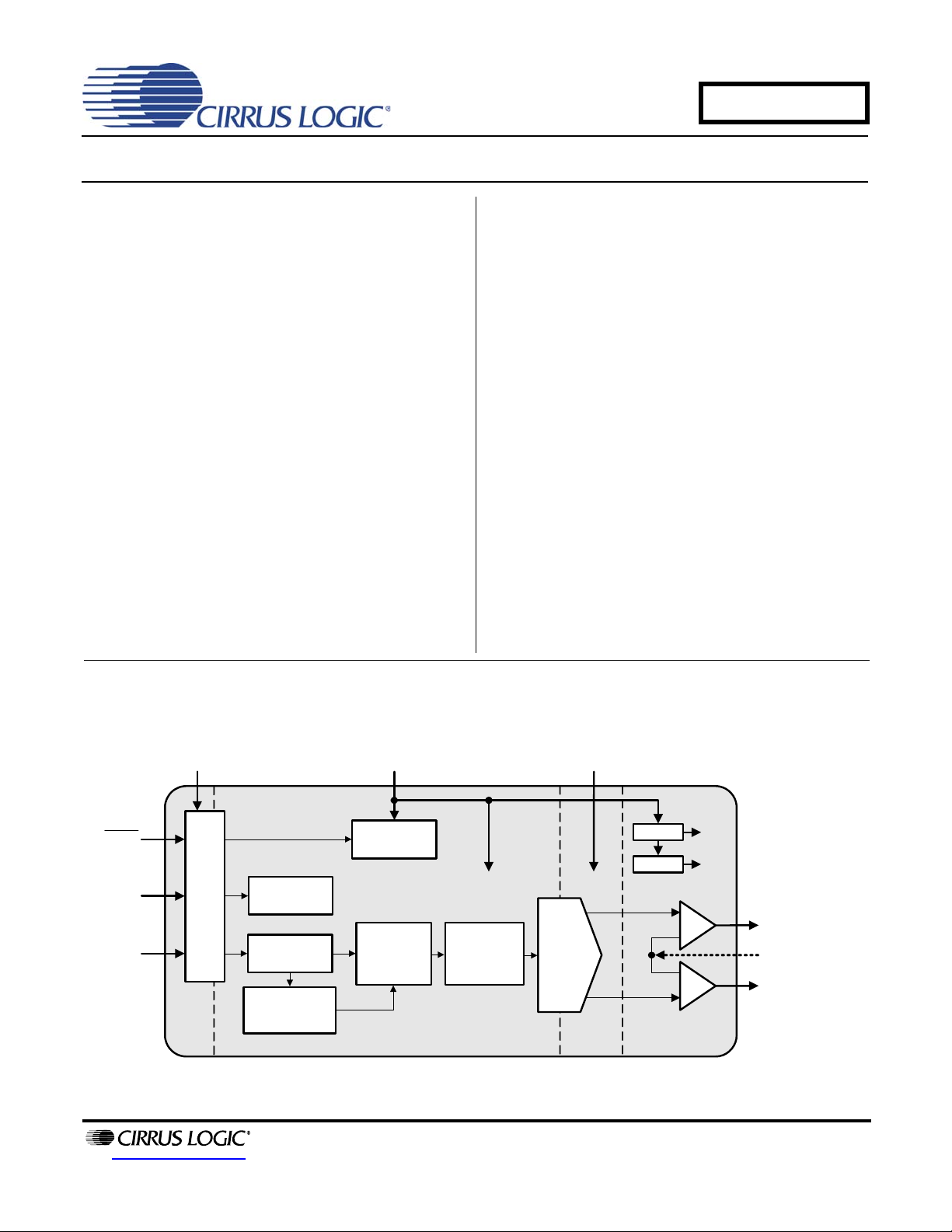
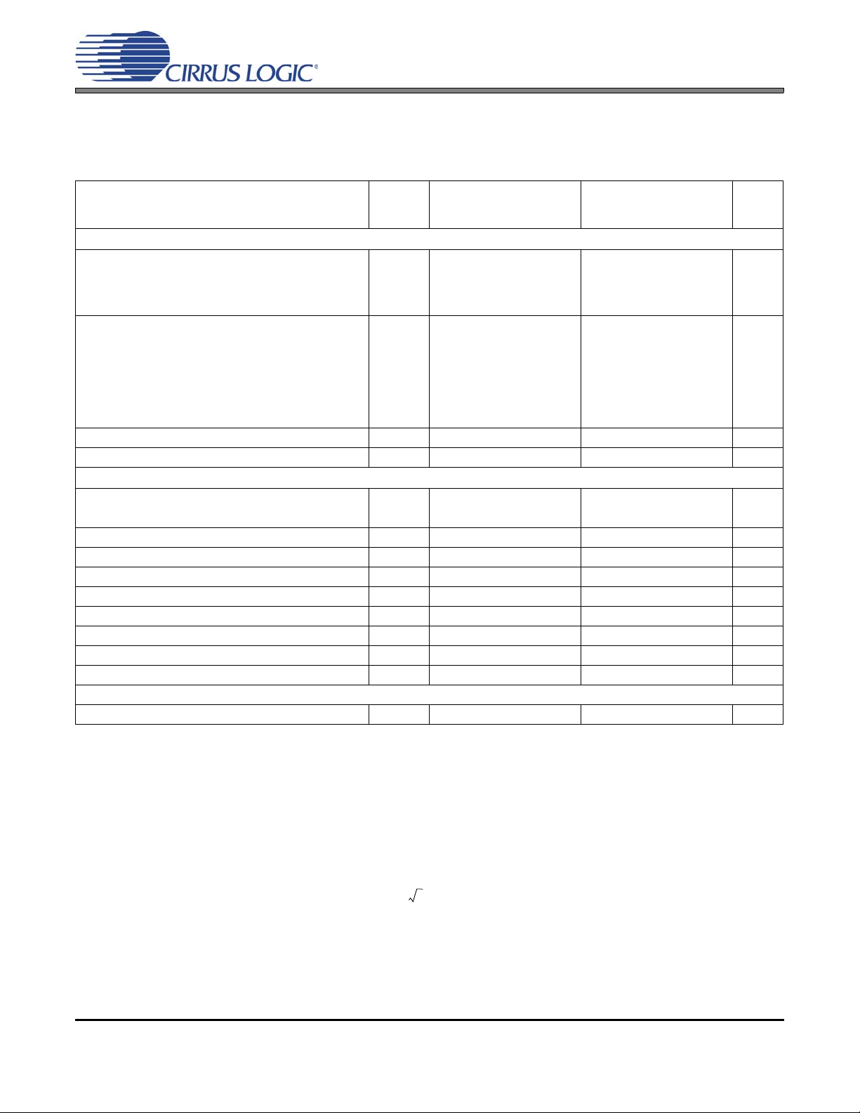
PCM Serial
Audio Port
Level Shifter
Serial
Audio
Input
Multibit
Modulator
Interpolation
Filters
Digital Core Logic and
Charge Pump Supply (VCP)
+3.3 V
Left Channel
Right Channel
Hardware
Control
Power-On
Reset
Hardware
Control
Reset
Auto Speed
Mode Detect
Analog Supply (VA)
+3.3 V
Inverting
Step-Up
+VA_H
-VA_H
Interface Supply (VL)
+0.9 V to +3.3 V
Ground-Centered,
2 Vrms Line Level Outputs
DAC
Pseudo Diff. Input
CS4353
3.3 V Stereo Audio DAC with 2 V
Features
Multi-bit Delta-Sigma Modulator
106 dB A-weighted Dynamic Range
-93 dB THD+N
Single-ended Ground Centered Analog
Architecture
– No DC-blocking Capacitors Required
– Integrated Step-up/Inverting Charge Pump
– Filtered Line-level Outputs
– Selectable 1 or 2 V
Low Clock-jitter Sensitivity
Low-latency Digital Filtering
Supports Sample Rates up to 192 kHz
24-bit Resolution
+3.3 V Charge Pump and Core Logic, +3.3 V
Analog, and +0.9 to 3.3 V Interface Power
Supplies
Low Power Consumption
24-pin QFN, Lead-free Assembly
Full-scale Output
RMS
Description
The CS4353 is a complete stereo digital-to-analog system including digital interpolation, fifth-order multi-bit
delta-sigma digital-to-analog conversion, digital de-emphasis, analog filtering, and on-chip 2 V
driver from a 3.3 V supply.
The advantages of this architecture include ideal differential linearity, no distortion mechanisms due to resistor
matching errors, no linearity drift over time and temperature, high tolerance to clock jitter, and a minimal set of
external components.
The CS4353 is available in a 24-pin QFN package in
Commercial (-40°C to +85°C) grade. The CDB4353
Customer Demonstration Board is also available for device evaluation and implementation suggestions.
Please see “Ordering Information” on page 25 for complete details.
These features are ideal for cost-sensitive, 2-channel
audio systems including video game consoles, DVD
players and recorders, A/V receivers, set-top boxes,
digital TVs, mini-component systems, and mixing
consoles.
RMS
Line Output
line-level
RMS
http://www.cirrus.com
Copyright Cirrus Logic, Inc. 2011
(All Rights Reserved)
MAY ‘11
DS803F3
Page 2

TABLE OF CONTENTS
1. PIN DESCRIPTIONS ............................................................................................................................. 4
2. CHARACTERISTICS AND SPECIFICATIONS ...................................................................................... 6
RECOMMENDED OPERATING CONDITIONS .................................................................................... 6
ABSOLUTE MAXIMUM RATINGS ........................................................................................................ 6
DAC ANALOG CHARACTERISTICS .................................................................................................... 7
COMBINED INTERPOLATION & ON-CHIP ANALOG FILTER RESPONSE ........................................ 8
SWITCHING SPECIFICATIONS - SERIAL AUDIO INTERFACE ................................................... 9
DIGITAL INTERFACE CHARACTERISTICS ....... ... ... .... ... ... ... .... ......................................... .... ... ... ... ... 10
INTERNAL POWER-ON RESET THRESHOLD VOLTAGES ............................................................. 10
DC ELECTRICAL CHARACTERISTICS .............................................................................................. 11
3. TYPICAL CONNECTION DIAGRAM ................................................................................................... 12
4. APPLICATIONS ................................................................................................................................... 13
4.1.1 Ground-centered Outputs ............................ .... .......................................... ... ... ...................... 13
4.1.2 Full-scale Output Amplitude Control ......................................................................................13
4.1.3 Pseudo-differential Outputs ... ... .......................................... ... ... .... ... ... ... .... ............................ 13
4.9.1 Power-up Sequences .. ... .... ... ... ... ... .... ... ................................................................................ 19
4.9.1.1 External RESET Power-up Sequence ....................................................................... 19
4.9.1.2 Internal Power-on Reset Power-up Sequence .......................................................... 19
4.9.2 Power-down Sequences .................... ................................................................................... 19
4.9.2.1 External RESET Power-down Sequence .................................................................. 19
4.9.2.2 Internal Power-on Reset Power-down Sequence ...................................................... 19
4.10.1 Capacitor Placement ........................................................................................................... 20
5. DIGITAL FILTER RESPONSE PLOTS ......................................................................................... 21
6. PARAMETER DEFINITIONS ................................................................................................................ 23
7. PACKAGE DIMENSIONS .................................................................................................................... 24
8. ORDERING INFORMATION ............................................................................................................... 25
9. REVISION HISTORY ........................................................................................................................... 25
CS4353
2 DS803F3
Page 3

LIST OF FIGURES
Figure 1.Serial Input Timing ........................................................................................................................ 9
Figure 2.Power-on Reset Threshold Sequence . .... ... ... ... .......................................................................... 10
Figure 3.Typical Connection Diagram ....................................................................................................... 12
Figure 4.Stereo Pseudo-differential Output ............................................................................................... 13
Figure 5.I²S, up to 24-bit Data ................................................................................................................... 15
Figure 6.Left-justified up to 24-bit Data ..................................................................................................... 15
Figure 7.De-emphasis Curve, Fs = 44.1 kHz ............................................................................................ 16
Figure 8.Internal Power-on Reset Circuit .................................................................................................. 16
Figure 9.Initialization and Power-down Sequence Diagram ............... ... ... ... .... ... ... ... .... ... ... ... ... .... ... ... ... ... 18
Figure 10.Single-speed Stopband Rejection ............................................................................................. 21
Figure 11.Single-speed Transition Band ................................................................................................... 21
Figure 12.Single-speed Transition Band (detail) ....................................................................................... 21
Figure 13.Single-speed Passband Ripple ................................................................................................. 21
Figure 14.Double-speed Stopband Rejection ........................................................................................... 21
Figure 15.Double-speed Transition Band ................................................................................................. 21
Figure 16.Double-speed Transition Band (detail) ..................................................................................... 22
Figure 17.Double-speed Passband Ripple ............................................................................................... 22
Figure 18.Quad-speed Stopband Rejection .............................................................................................. 22
Figure 19.Quad-speed Transition Band .................................................................................................... 22
Figure 20.Quad-speed Transition Band (detail) ........................................................................................ 22
Figure 21.Quad-speed Passband Ripple .. ... ... ... .... ... ... ... .... ... ... ... .... ... ... ... ... .... ... ... ... .... ... ... ... ... .... ... ......... 22
CS4353
LIST OF TABLES
Table 1. Digital I/O Pin Characteristics .................. ... ... ... .... .......................................... ... ... ...................... 11
Table 2. CS4353 Operational Mode Auto-Detect ...................................................................................... 14
Table 3. Single-speed Mode Standard Frequencies .................... .... ... ... ... ... .... ... ...................................... 14
Table 4. Double-speed Mode Standard Frequencies ............................................................................... 14
Table 5. Quad-speed Mode Standard Frequencies ..................................................................................14
Table 6. Digital Interface Format ............... .......................................... ...................................................... 15
DS803F3 3
Page 4
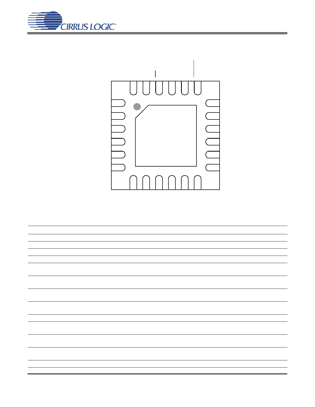
1. PIN DESCRIPTIONS
87
6
5
4
3
2
1
9
10
11 12
19
2021222324
13
14
15
16
17
18
Top-Down (Through Package) View
24-Pin QFN Package
SDIN
LRCK
I²S
/LJ
DEM
1_2VRMS
RESET
FLYP+
VFILT+
FLYN+
CPGND
FLYN-
SCLK
MCLK
VL
DGND
FLYP-
VBIAS
VA
AGND
AOUT_REF
AOUTB
Thermal Pad
VCP
VFILT-
AOUTA
CS4353
Pin Name Pin # Pin Description
SCLK 1 Serial Clock (Input) - Serial clock for the serial audio interface.
MCLK 2 Master Clock (Input) - Clock source for the delta-sigma modulator and digital filters.
VL 3 Serial Audio Interface Power (Input) - Positive power for the serial audio interface
DGND 4 Digital Ground (Input) - Ground reference for the digital section.
FL YP+
FL YPVCP 6
VFILT+ 8
FLYN+
FLYNCPGND 10 Charge Pump Ground (Input) - Ground reference for the Charge Pump section.
VFILT- 12
AOUTB
AOUTA
AOUT_REF 14
AGND 16 Analog Ground (Input) - Ground reference for the low voltage analog section.
4 DS803F3
75Step-up Charge Pump Cap Positive/Negative Nodes (Output) - Positive and Negative nodes for the
step-up charge pump’s flying capacitor.
Charge Pump and Digital Core Logic Power (Input) - Positive power supply for the step-up and invert-
ing charge pumps as well as the digital core logic sections.
Step-up Charge Pump Filter Connection (Output) - Power supply from the step-up charge pump that
provides the positive rail for the output amplifiers
911Inverting Charge Pump Cap Positive/Negative Nodes (Output) - Positive and Negative nodes for the
1315Analog Outputs (Output) - The full-scale analog line output level is specified in the Analog Characteris-
inverting charge pump’s flying capacitor.
Inverting Charge Pump Filter Connection (Output) - Power supply from the inverting charge pump that
provides the negative rail for the output amplifiers.
tics table.
Pseudo Diff. Analog Output Reference (Input) - Ground reference for the analog output amplifiers.
This pin must be at the same nominal DC voltage as the AGND pin.
Page 5
VA 17 Low Voltage Analog Power (Input) - Positive power supply for the analog section.
VBIAS 18 Positive Voltage Reference (Output) - Positive reference voltage for the internal DAC.
Reset (Input) - Optional connection for an external reset control. The device enters a powered-down
RESET
state when this pin is set low (GND) OR when the VCP supply falls below the V
19
“Internal Power-on Reset Threshold Voltages” on page 10.). This pin should be set high (VL) during nor-
threshold (see See
off
mal operation.
1_2VRMS 20
DEM 21
/LJ 22
I²S
LRCK 23
1 or 2 V
selects 1 V
De-emphasis (Input) - Selects the standard 50 s/15 s digital de-emphasis filter response for 44.1 kHz
sample rates when enabled.
Digital Interface Format (Input) - Selects the serial audio interface format. Setting this pin low (GND)
selects I²S, while setting it high (VL) selects Left-Justified.
Left / Right Clock (Input) - Determines which channel, Left or Right, is currently active on the serial
audio data line.
Select (Input) - Selects the analog output full-scale voltage. Setting this pin low (GND)
RMS
, while setting it high (VL) selects 2 V
RMS
RMS
.
SDIN 24 Serial Audio Data Input (Input) - Input for two’s complement serial audio data.
Thermal Pad -
Thermal Relief Pad - This pad may be soldered to the board, however it MUST be electrically isolated
from all board connections.
CS4353
DS803F3 5
Page 6
CS4353
2. CHARACTERISTICS AND SPECIFICATIONS
RECOMMENDED OPERATING CONDITIONS
AGND = DNGD = CPGND = 0 V; all voltages with respect to ground.
Parameters Symbol Min Typ Max Units
DC Power Supply Charge Pump an d Digital Core power (Note 1)
Low Voltage Analog power (Note 1)
Interface power
Ambient Operating Temperature (Power Applied) T
VCP
VA
VL
A
3.13
3.13
0.85
-40 - +85 °C
3.3
3.3
0.9 to 3.3
3.47
3.47
3.47
V
V
V
Note: 1. VCP and VA must be supplied with the same nominal voltage. Additional current draw will occur if the sup-
ply voltages applied to VCP and VA differ by more than 0.5 V.
ABSOLUTE MAXIMUM RATINGS
AGND = DNG D = C P GN D = 0V; all voltages with respect to ground.
Parameters Symbol Min Max Units
DC Power Supply Charge Pump and Digital Core Logic Power
Low Voltage Analog Power
Supply Voltage Difference
Interface Power
Input Current, Any Pin Except Supplies I
Digital Input Voltage Digital Interface V
Analog Input Voltage AOUT_REF V
Ambient Operating Temperature (Power Applied) T
Storage Temperature T
WARNING:Operation at or beyond these limits may result in permanent damage to the device. Normal operation
is not guaranteed at these extremes.
VCP
VA
|VCP - VA|
VL
in
IN-L
IN-A
A
stg
-0.3
-0.3
-
-0.3
-±10mA
-0.3 VL+ 0.4 V
-0.3 0.5 V
-55 +125 °C
-65 +150 °C
3.63
3.63
0.5
3.63
V
V
V
V
6 DS803F3
Page 7
CS4353
VRMS
Vpp
22
----------=
DAC ANALOG CHARACTERISTICS
Test conditions (unless otherwise specified): TA = 25 °C; VCP = VA = 3.3 V; AOUT_REF = AGND = DGND =
CPGND = 0V; VBIAS, VFILT+/-, and FLYP/N+/- capacitors as shown in Figure 3 on page 12; input test signal is a
997 Hz sine wave at 0 dBFS; measurement bandwidth 10 Hz to 20 kHz.
1_2VRMS = 0 1_2VRMS = 1
Parameter Symbol Min Typ Max Min Typ Max Unit
Dynamic Performance, Fs = 48, 96, and 192 kHz (Notes 2, 3, 4)
Dynamic Range 24-bit A-Weighted
unweighted
16-bit A-Weighted
unweighted
Total Harmonic Distortion + Noise
24-bit 0 dB
-20 dB
-60 dB
16-bit 0 dB
-20 dB
-60 dB
Idle Channel Noise / Signal-to-Noise Ratio (A-wt) - 100 - - 106 - dB
Interchannel Isolation (1 kHz) - 115 - - 115 - dB
THD+N
Analog Output (Note 5)
Full Scale AOUTx Output Voltage (Notes 4, 6, 7) 1.021.081.132.042.152.26V
Max Current Draw from an AOUTx Pin I
Interchannel Gain Mismatch - 0.1 - - 0.1 - dB
Output Offset - ±5 ±8 - ±5 ±8 mV
Gain Drift - 100 - - 100 - ppm/°C
Output Impedance Z
AC-Load Resistance R
Load Capacitance C
AOUT_REF Rejection (Notes 8, 9)AOR-40- -40-dB
Analog Reference Input
AOUT_REF Input Voltage (Note 10) --0.2--0.2Vpp
OUTmax
OUT
L
L
94
91
2.89 3.05 3.20 5.78 6.09 6.40 V
5--5--k
100
97
-
-
-
-
-
-
-
-
-
-575- -575- A
-100- -100-
- - 1000 - - 1000 pF
92
89
-93
-77
-37
-93
-75
-29
-87
-71
-31
-
100
-
-
-
-
-
-
97
106
103
-
-
-
-
-
-
-
-
-
98
95
-93
-83
-43
-93
-75
-35
-
-
-
-
-87
-77
-37
-
-
-
dB
dB
dB
dB
dB
dB
dB
dB
dB
dB
RMS
pp
Notes: 2. Measured at the output of the external LPF on AOUTx as shown in Figure 3 on page 12.
3. One LSB of triangular PDF dither is added to data.
4. Measured with the specified minimum AC-Load Resistance present on the AOUTx pins.
5. Measured between the AOUTx and AOUT_REF pins.
6. External impedance between the AOUTx pin and the load will lower the voltage delivered to the load.
7. V
is the controlling specification. V
PP
specification valid for sine wave signals only.
RMS
Note that for sine wave signals:
8. Measured with AOUT_REF connected directly to ground. External impedance between AOUT_REF
and ground will lower the AOUT_REF rejection.
DS803F3 7
Page 8
CS4353
AOR
dB
20 log
10
AOUT_REF
AOUT_REF A OUTx–
---------------------------------------------------------
=
9. SDIN = 0. AOUT_REF input test signal is a 60 Hz, 50 mVpp sine wave. Measured by applying the test
signal into the AOUT_REF pin and measuring the resulting output amplitude on the AOUTx pin. Specification calculated by:
10. Applying a DC voltage on the AOUT_RE F pin will cause a DC offset on the DAC output. See Section
4.1.3 for more information.
COMBINED INTERPOLATION & ON-CHIP ANALOG FILTER RESPONSE
The filter characteristics have been norma lized to th e sample rate (Fs) and can be referenced to the desired sample rate by multiplying the given characteristic by Fs.
Parameter Min Typ Max Unit
Single-Speed Mode - 48 kHz
Passband (Note 11) to -0.01 dB corner
to -3 dB corner
Frequency Response 10 Hz to 20 kHz -0.01 - +0.01 dB
StopBand 0.547 - - Fs
StopBand Attenuation (Note 12) 102 - - dB
Total Group Delay (Fs = Sample Rate) - 9.4/Fs - s
Intra-channel Phase Deviation - - ±0.56/Fs s
Inter-channel Phase Deviation - - 0 s
De-emphasis Error (Note 13) (Relative to 1 kHz) Fs = 44.1 kHz - - ±0.14 dB
Double-Speed Mode - 96 kHz
Passband (Note 11) to -0.01 dB corner
to -3 dB corner
Frequency Response 10 Hz to 20 kHz -0.01 - 0.01 dB
StopBand .583 - - Fs
StopBand Attenuation (Note 12) 80 - - dB
Total Group Delay (Fs = Sample Rate) - 4.6/Fs - s
Intra-channel Phase Deviation - - ±0.03/Fs s
Inter-channel Phase Deviation - - 0 s
Quad-Speed Mode - 192 kHz
Passband (Note 11) to -0.01 dB corner
to -3 dB corner
Frequency Response 10 Hz to 20 kHz -0.01 - 0.01 dB
StopBand .635 - - Fs
StopBand Attenuation (Note 12) 90 - - dB
Total Group Delay (Fs = Sample Rate) - 4.7/Fs - s
High-Pass Filter Characteristics
Passband (Note 11) to -0.05 dB corner
to -3 dB corner
Passband Ripple - - 0.01 dB
Phase Deviation @ 20 Hz - - 1.34 Deg
Filter Settling Time (input signal goes to 95% of its final value) - 5x10
Notes: 11. Response is clock-dependent and will scale with Fs.
12. For Single- and Double-Speed Mode, the Measurement Bandwidth is from stop band to 3 Fs.
For Quad-Speed Mode, the Measurement Bandwidth is from stopband to 1.34 Fs.
13. De-emphasis is available only in Single-Speed Mode.
14. Amplitude vs. Frequency plots of this data are available in “Digital Filter Response Plots” on page 21.
0
0
0
0
0
0
9.00x10
9.74x10
-
-
-
-
-
-
-5
-6
-
-
4
/Fs - s
.454
.499
.430
.499
.105
.490
-
-
Fs
Fs
Fs
Fs
Fs
Fs
Fs
Fs
8 DS803F3
Page 9

CS4353
sclkh
t
slrs
t
slrd
t
sdlrs
t
sdh
t
sclkl
t
SDATA
SCLK
LRCK
Figure 1. Serial Input Timing
1
128Fs
--------------------- -
1
64Fs
------------------
1
64Fs
------------------
SWITCHING SPECIFICATIONS - SERIAL AUDIO INTERFACE
Parameters Symbol Min Max Units
MCLK Frequency 2.048 51.2 MHz
MCLK Duty Cycle 45 55 %
Input Sample Rate (Auto selection) Single-Speed Mode
Double-Speed Mode
Quad-Speed Mode
LRCK Duty Cycle 40 60 %
SCLK Pulse Width Low t
SCLK Pulse Width High t
SCLK Period Single-Speed Mode - s
Double-Speed Mode - s
Quad-Speed Mode - s
Fs
Fs
Fs
sclkl
sclkh
8
84
170
20 - ns
20 - ns
54
108
216
kHz
kHz
kHz
SCLK rising to LRCK edge delay t
SCLK rising to LRCK edge setup time t
SDIN valid to SCLK rising setup time t
SCLK rising to SDIN hold time t
slrd
slrs
sdlrs
sdh
20 - ns
20 - ns
20 - ns
20 - ns
DS803F3 9
Page 10

CS4353
VCP
V
on2
V
on1
V
off
DGND
HI
LO
No Power
reset
undefined
reset
active
DAC
Ready
reset
active
reset
(internal)
DIGITAL INTERFACE CHARACTERISTICS
Test conditions (unless otherwise specified): AGND = DGND = CPGND = 0V; all voltages with respect to ground.
Parameters Symbol Min Typ Max Units
High-Level Input Voltage 1.2 V <VL 3.3 V
0.9 V VL 1.2 V
Low-Level Input Voltage 1.2 V <VL 3.3 V
0.9 V VL 1.2 V
Input Leakage Current I
Input Capacitanc e - 8 - pF
V
IH
V
IH
V
IL
V
IL
in
0.7xVL
0.9xVL
-
-
-
-
-
-
-
-
0.3xVL
0.1xVL
--±10A
V
V
V
V
INTERNAL POWER-ON RESET THRESHOLD VOLTAGES
Test conditions (unless otherwise specified): AGND = DGND = CPGND = 0V; all voltages with respect to ground.
Parameters Symbol Min Typ Max Units
Internal Reset Asserted at Power-On
Internal Reset Released at Power-On
Internal Reset Asserted at Power-Off
V
on1
V
on2
V
off
-1.00- V
-2.36- V
-2.22- V
Figure 2. Power-on Reset Threshold Sequence
10 DS803F3
Page 11

CS4353
DC ELECTRICAL CHARACTERISTICS
Test conditions (unless otherwise specified): VCP = VA = VL = 3.3 V; AGND = DGND = CPGND = 0V; SDIN = 0;
all voltages with respect to ground.
Parameters Symbol Min Typ Max Units
Power Supplies
Power Supply Current (Note 15)
Normal Operation
Power-Down, All Supplies (Note 16)
Power Dissipation (All Supplies) Normal Operation, 1_2VRMS = 0
(Note 15) Power-Down (Note 16)
Power Supply Rejection Ratio (Note 17) (1 kHz)
(60 Hz)
I
VCP
I
VA
I
VL
I
PD
PSRR -
-
-
-
-
-
-
-
DC Output Voltages
Pin Voltage FLYP+ to FLYP-
VFILT+ to GND (Note 18)
FL YN+ to FLYN-
GND to VFILT- (Note 18)
VA to VBIAS
-
-
-
-
-
Notes: 15. Current consumption increases with increasing sample rate and increasing MCLK frequency. Typical
values are based on Fs = 48 kHz and MCLK = 12.288 MHz. Maximum values are based on highest
sample rate and highest MCLK frequency; see Switching Specifications - Serial Audio Interface. Variance between speed modes is small.
16. Power-down is defined as RESET
pin = Low with all clock and data lines held static low. All digital inputs
have a weak pull-down (approximately 50 k) which is only presen t during reset. Opp osing this pulldown will slightly increase the power-down current.
17. Valid with the recommended capacitor value on VBIAS
as shown in the typical connectio n diagram in
Section 3.
18. Typical voltage shown for “Initialization State”; see Section 4.8. Typical voltage may be up to 1.5 V lower
during normal operation.
36
2.4
0.1
65
127
1
60
60
3.3
6.6
6.6
6.6
2.1
43
3
0.2
-
152
-
-
-
-
-
-
-
-
mA
mA
mA
A
mW
mW
dB
dB
V
V
V
V
V
2.1 Digital I/O Pin Characteristics
Input and output levels and associated power supply vo lta ge are shown in Table1. Logic levels should not
exceed the corresponding power supply voltage.
Pin Name Power Supply I/O Driver Receiver
RESET
MCLK Input - 0.9 V - 3.3 V
LRCK Input - 0.9 V - 3.3 V
SCLK Input - 0.9 V - 3.3 V
SDIN Input - 0.9 V - 3.3 V
DEM Input - 0.9 V - 3.3 V
/LJ Input - 0.9 V - 3.3 V
I²S
1_2VRMS Input - 0.9 V - 3.3 V
VL
Table 1. Digital I/O Pin Characteristics
DS803F3 11
Input - 0.9 V - 3.3 V, with Hysteresis
Page 12

3. TYPICAL CONNECTION DIAGRAM
VL+0.9 V to +3.3 V
RESET
LRCK
MCLK
SCLK
AOUT_REF
SDIN
VFILT-
AOUTA
V
A
562
2.2 nF
R
ext
R
ext
Line Level Out
Left & Right
I²S/LJ
DEM
1_2VRMS
VFILT+
Digital Audio
Processor
Hardware
Control
Values shown are for
Fc = 130 kHz.
Capacitors must be
C0G or equivalent.
562
2.2 nF
AOUTB
VBIAS
FLYN-
FLYN+
0.1 µF
0.1 µF
2.2 µF
FLYP-
FLYP+
2.2 µF
0.1 µF
0.1 µF
+3.3 V
0.1 µF
V
C
P
Note 1:
C
P
G
N
D
D
G
N
D
A
G
ND
22 µF
2.2 µF
2.2 µF
2.2 µF
Note 1
3
1
2
23
24
22
19
21
20
10 4 16
18
176
12
11
9
13
14
15
5
7
8
+
+
+
Note 2
Note 2:
Connect RESET
to VL if internal
power-on reset is
used.
+
CS4353
Figure 3. Typical Connection Diagram
CS4353
12 DS803F3
Page 13

4. APPLICATIONS
Internal Left
DAC Signal
AOUTA
AOUT_REF
//
//
Left Output
GND
(pseudo-differential traces)
AOUTB
//
Right Output
(pseudo-differential traces)
Internal Right
DAC Signal
Psuedo-differential output improves common
mode rejection, reducing external system noise
Figure 4. Stereo Pseudo-differential Output
4.1 Line Outputs
4.1.1 Ground-centered Outputs
An on-chip charge pump creates both positive and negative high-voltage supplies, which allows the fullscale output swing to be centered around ground. This eliminates the need for large DC-blocking capacitors which create audible pops at power-on, allows the CS4353 to deliver a larger full-scale output at lower supply voltages, and provides improved bandwidth frequency response .
4.1.2 Full-scale Output Amplitude Control
The full-scale output voltage amplitude is selected via the 1_2VRMS pin. When the pin is connected to
VL, the full-scale output voltage at the AOUTx pins is approximately 2 V
to GND, the full-scale output voltage at the AOUTx pins is approximately 1 V
between the AOUTx pin and the load will lower the voltage delivered to the load. See the DAC Analog
Characteristics table for the complete specifications of the full-scale output voltage.
4.1.3 Pseudo-differential Outputs
The CS4353 implements a pseudo-differential output stage. The AOUT_REF input is intended to be used
as a pseudo-differential reference signal. This featur e provides common mode noise rejection with singleended signals. Figure 4 shows a basic diagram outlining the internal implementation of the pseudo-differential output stage, including a recommended stereo pseudo-differ ential output topology. If pseudo-differential output functionality is not required, simply connect the AOUT_REF pin to ground next to the
CS4353. If a split-ground design is used, the AOUT_REF pin should be connected to AGND. See the Ab-
solute Maximum Ratings table for the maximu m allowable voltag e on the AOUT_REF pin. Applying a DC
voltage on the AOUT_REF pin will cause a DC offset on the DAC output.
CS4353
. When the pin is connected
RMS
. Additional impedance
RMS
DS803F3 13
Page 14

4.2 Sample Rate Range/Operational Mode Detect
The CS4353 operates in one of three operational modes. The device will auto-detect the correct mode when
the input sample rate (Fs), defined by the LRCK frequency, falls within one of the ranges illustrated in
Table 2. Sample rates outside the specified range for each mode are not supported. In addition to a valid
LRCK frequency, a valid serial clock (SCLK) and master clock (MCLK) must also be applied to the device
for speed mode auto-detection; see Figure 9.
Input Sample Rate (Fs) Mode
8 kHz - 54 kHz Single-Speed Mode
84 kHz - 108 kHz Double-Speed Mode
170 kHz - 216 kHz Quad-Speed Mode
T able 2. CS4353 Operational Mode Auto-Detect
4.3 System Clocking
The device requires external generation of the master (MCLK), left/right (LRCK) and serial (SCLK) clocks.
The left/right clock, defined also as the input sample rate (Fs), must be synchronously derived from the
MCLK signal according to specified ratios. The specified ratios of MCLK to LRCK, along with several standard audio sample rates and the required MCLK frequency, are illustrated in Tables 3-5.
Refer to Section 4.4 for the required SCLK timing associated with the selected Digital Interface Format and
to “Switching Specifications - Serial Audio Interface” on page 9 for the maximum allowed clock frequencies.
CS4353
Sample Rate
(kHz)
32 8.1920 12.2880 16.3840 24.5760 32.7680
44.1 1 1.2896 16.9344 22.5792 33.8688 45.1584
48 12.2880 18.4320 24.5760 36.8640 49.1520
256x 384x 512x 768x 1024x
Table 3. Single-speed Mode Standard Frequencies
Sample Rate
(kHz)
88.2 11.2896 16.9344 22.5792 33.8688 45.1584
96 12.2880 18.4320 24.5760 36.8640 49.1520
128x 192x 256x 384x 512x
Table 4. Double-speed Mode Standard Frequencies
Sample Rate
(kHz)
176.4 22.5792 33.8688 45.1584
192 24.5760 36.8640 49.1520
T able 5. Quad-speed Mode Standard Frequencies
128x 192x 256x
MCLK (MHz)
MCLK (MHz)
MCLK (MHz)
14 DS803F3
Page 15

4.4 Digital Interface Format
LRCK
SCLK
Left Channel
Right Channel
SDIN +3 +2 +1+5 +4
MSB
-1 -2 -3 -4 -5
+3 +2 +1+5 +4
-1 -2 -3 -4
MSB
LSB
LSB
LRCK
SCLK
Left Channel
Right Channel
SDIN +3 +2 +1+5 +4
MSB
-1 -2 -3 -4 -5
+3 +2 +1+5 +4
-1 -2 -3 -4
LSB
MSB
LSB
The device will accept audio samples in either I²S or Left-Justified digital interface formats, as illustrated in
Table 6.
CS4353
The desired format is selected via the I²S
/LJ pin. For an illustration of the required relationship between the
LRCK, SCLK and SDIN, see Figures 5-6. For all formats, SDIN is valid on the rising edge of SCLK. Also,
SCLK must have at least 32 cycles per LRCK period in the Left-Justified format.
For more information about serial audio formats, refe r to Cirrus Logic Application Note AN282: The 2-Chan-
nel Serial Audio Interface: A Tutorial, available at http://www.cirrus.com.
I²S
/LJ
0
I²S, up to 24-bit Data
1
Left-Justified, up to 24-bit Data
Table 6. Digital Interface Format
Description Figure
5
6
Figure 5. I²S, up to 24-bit Data
4.5 Internal High-Pass Filter
The device includes an internal digital high-pass filter. This filter prevents a constant digital offset from creating a DC voltage on the analog output pins. The filter’s corner frequency is well be low the audio band; see
the Combined Interpolation & On-Chip Analog Filter Response table for filter specifications.
DS803F3 15
Figure 6. Left-justified up to 24-bit Data
Page 16

4.6 De-emphasis Control
Gain
dB
-10dB
0dB
Frequency
T2 = 15 µs
T1=50 µs
F1 F2
3.183 kHz 10.61 kHz
Figure 7. De-emphasis Curve, Fs = 44.1 kHz
RESET
(external)
Power-On Reset
Circuit
VCP
DGND
reset
(internal)
The device includes on-chip digital de-emphasis. Figure 7 shows the de-emphasis curve for Fs equal to
44.1 kHz. The frequency response of the de-emphasis curve scales with changes in the sample rate, Fs.
The de-emphasis error will increase for sample rates other than 44.1 kHz.
When the DEM pin is connected to VL, the 44.1 kHz de-emphasis filter is activated. When the DEM pin is
connected to GND, the de-emphasis filter is turned off.
Note: De-emphasis is only available in Single-Speed Mode.
CS4353
4.7 Internal Power-on Reset
The CS4353 features an internal power-on reset (POR) circuit. Th e POR circuit allows the RESET pin to be
connected to VL during power-up and power-down sequences if the external reset function is not needed.
This circuit monitors the VCP supply a nd automatically as serts or releases an internal reset of th e DAC’s
digital circuitry when the supply reaches defined thresholds (see “Internal Power-on Reset Thre sho l d Volt-
ages” on page 10). No external clocks are required for the POR circuit to function.
Figure 8. Internal Power-on Reset Circuit
When power is first applied, the POR circuit monitors the VCP supply voltage to determine when it reaches
a defined threshold, V
digital circuitry. Once the VCP supply reaches the secondary threshold, V
internal reset.
Note: For correct operation o f the internal POR circuit, the voltage on VL must rise before or simulta-
neously with VCP.
16 DS803F3
When power is removed and the VCP voltage reaches a de fined thresh old, V
internal reset low, resetting all of the digital circuitry.
. At this time, the POR circuit asserts the internal reset low, resetting all of the
on1
, the POR circuit releases the
on2
, the POR circuit asserts the
off
Page 17

4.8 Initialization
When power is first applied, the DAC enters a reset (low power) state at the beginning of the initialization
sequence. In this state, the AOUTx pins are weakly pulled to ground and VBIAS is connected to VA.
CS4353
The device will remain in the reset state until the RESET
the internal digital circuitry is reset and the DAC enters a power-down state until MCLK is applied. Alternatively, if no external reset control is required, the internal power-on reset can be used by tying the RESET
pin to VL (see Section 4.7).
Once MCLK is valid, the device enters an initialization state in which the charge p ump powers up and charges the capacitors for both the positive and negative high-voltage supplies.
Once LRCK and SCLK are valid, the number of MCLK cycles is counted relative to the LRCK pe riod to determine the MCLK/LRCK frequency ratio. Next, the device enters the power-up state in which the interpolation and decimation filters and delta-sigma modulators are turned on, the internal voltage reference,
VBIAS, powers up to normal operation, the analog output pull-down resistors are removed, and power is
applied to the output amplifiers.
After this power-up state sequence is complete, normal operation begins and analog output is generated.
If valid MCLK, LRCK, and SCLK are applied to the DAC before RESET
SET being set high to the analog audio output from AOUTx is less than 50 ms.
See Figure 9 for a diagram of the device’s states and transition conditions.
pin is brought high. Once the RESET pin is high,
is set high, the total time from RE-
DS803F3 17
Page 18

USER: Apply Power
USER: Apply MCLK
MCLK/LRCK Ratio Detection
USER: Apply LRCK and SCLK
Reset State
Power-Down State
Initialization State
Power-Up State
Outputs Grounded
Normal Operation State
Mute State
Valid MCLK/LRCK Ratio
or
USER: RESET Set High
RESET Tied High (if using POR)
USER: Change MCLK/LRCK ratio
Outputs Muted
Analog Output Generated
USER: RESET
Set Low
USER: Change MCLK/LRCK ratio
Valid MCLK/LRCK Ratio
or
Remove MCLK
Figure 9. Initialization and Power-down Sequence Diagram
CS4353
18 DS803F3
Page 19

4.9 Recommended Power-up and Power-down Sequences
4.9.1 Power-up Sequences
4.9.1.1 External RESET Power-up Sequence
Follow the power-up sequence below if the external RESET pin is used:
1. Hold RESET
The VA and VCP supplies should be applied prior to or simultaneously with the VL supply. If the VL
supply is applied before the VA and VCP supplies, a DC offset will occur on the analog outputs. The
offset level is bimodal: either approximately 0.7 V below the VL supply or app roximately 50 m V. The
first case can only occur if the VL supply is greater than approximately 1.2 V. Either offset level is
removed when the VA and VCP supplies are applied.
2. Set the I²S
3. Provide the correct MCLK, LRCK, and SCLK signals locked to the appropriate frequencies as
discussed in Section 4.3.
4. After the power supplies, configuration pins, and clock signals are stable, bring RESET
device will initiate the power-up sequence seen in Figure 9. The sequence will complete and audio
will be output from AOUTx within 50 ms after RESET
low while the power supplies are turned on.
/LJ, 1_2VRMS, and DEM configuration pins to the desired state.
is set high.
4.9.1.2 Internal Power-on Reset Power-up Sequence
CS4353
high. The
Follow the power-up sequence below if the internal power-on reset is used:
1. Hold RESET
The VA and VCP supplies should be applied prior to or simultaneously with the VL supply. If the VL
supply is applied before the VA and VCP supplies, a DC offset will occur on the analog outputs. The
offset level is bimodal: either approximately 0.7 V below the VL supply or app roximately 50 m V. The
first case can only occur if the VL supply is greater than approximately 1.2 V. Either offset level is
removed when the VA and VCP supplies are applied.
The power-on reset circuitry will function as described in Section 4.7.
2. Set the I²S
3. After the power supplies and configuration pins are stable, provide the correct MCLK, LRCK, and
SCLK signals to progress from the ‘Power-Down State’ in the power-up sequence seen in Figure 9.
The sequence will complete and audio will be output from the AOUTx pins within 50 ms after valid
clocks are applied.
high (connected to VL) while the power supplies are turned on.
/LJ, 1_2VRMS, and DEM configuration pins to the desired state.
4.9.2 Power-down Sequences
4.9.2.1 External RESET
Follow the power-down sequence below if the external RESET pin is used:
1. For minimal pops, set the input digital data to zero for at least 8192 consecutive samples.
2. Bring RESET
3. Remove the power supply voltages.
low.
Power-down Sequence
4.9.2.2 Internal Power-on Reset Power-down Sequence
Follow the power-down sequence below if the internal power-on reset is used:
1. For minimal pops, set the input digital data to zero for at least 8192 consecutive samples.
DS803F3 19
Page 20

2. Remove the MCLK signal without applying any glitched pulses to the MCLK pin.
3. Remove the power supply voltages.
Note: A glitched pulse is any pulse that is shorter than the period defined by the minimum/maximum
MCLK signal duty cycle specification and the nominal frequency of the input MCLK signal. A transient may occur on the analog outputs if the MCLK signal duty cycle specification is violated
when the MCLK signal is removed during normal operatio n; see “Switching Specifications - Serial
Audio Interface” on page 9.
4.10 Grounding and Power Supply Arrangements
As with any high-resolution converter, the CS4353 requir es careful attention to power supply and grounding
arrangements if its potential performance is to be realized. Figure 3 shows the recommended power arrangements, with VCP, VA, and VL connected to clean supplies. It is strongly recommended that a single
ground plane be used, with the DGND, CPGND, an d AGND pins all connected to this common plane.
Should it be necessary to split the ground planes, the DGND and CPGND pins should be connected to the
digital ground plane and the AGND pin should be connected to the analog ground plane. In this configuration, it is critical that the digital and analog ground planes be tied together with a low-impedance connection,
ideally a strip of copper on the printed circuit board, at a single point near the CS4353.
All signals, especially clocks, should be kept away from the VBIAS pin in order to avoid unwanted coupling
into the DAC.
CS4353
4.10.1 Capacitor Placement
Decoupling capacitors should be placed as close to the device as possible, with the low-value ceramic
capacitor being the closest. To further minimize impedance, these capacitors should be located on the
same PCB layer as the device. If desired, all supply pins may be connected to the same supply, but a
decoupling capacitor should still be placed on each supply pin. See DC Electrical Characteristics for the
voltage present across pin pairs. This is useful for choosing appropriate capacitor voltage ratings and orientation if electrolytic capacitors are used.
The CDB4353 evaluation board demonstrates the optimum layout and power supply arrangements.
20 DS803F3
Page 21

5. DIGITAL FILTER RESPONSE PLOTS
0.4 0.5 0.6 0.7 0.8 0.9 1
−120
−100
−80
−60
−40
−20
0
Frequency(normalized to Fs)
Amplitude (dB)
0.4 0.42 0.44 0.46 0.48 0.5 0.52 0.54 0.56 0.58 0.6
−120
−100
−80
−60
−40
−20
0
Frequency(normalized to Fs)
Amplitude (dB)
Figure 10. Single-speed Stopband Rejection Figure 11. Single-speed Transition Band
0.45 0.46 0.47 0.48 0.49 0.5 0.51 0.52 0.53 0.54 0.55
−10
−9
−8
−7
−6
−5
−4
−3
−2
−1
0
Frequency(normalized to Fs)
Amplitude (dB)
0 0.05 0.1 0.15 0.2 0.25 0.3 0.35 0.4 0.45 0.5
−0.02
−0.015
−0.01
−0.005
0
0.005
0.01
0.015
0.02
Frequency(normalized to Fs)
Amplitude (dB)
Figure 12. Single-speed Transition Band (d etail) Figure 13. Single-speed Passband Ripple
0.4 0.5 0.6 0.7 0.8 0.9 1
120
100
80
60
40
20
0
Frequency(normalized to Fs)
Amplitude (dB)
0.4 0.42 0.44 0.46 0.48 0.5 0.52 0.54 0.56 0.58 0.6
120
100
80
60
40
20
0
Frequency(normalized to Fs)
Amplitude (dB)
Figure 14. Double-speed Stopband Rejection Figure 15. Double-speed Transitio n Band
CS4353
DS803F3 21
Page 22

0.45 0.46 0.47 0.48 0.49 0.5 0.51 0.52 0.53 0.54 0.55
10
9
8
7
6
5
4
3
2
1
0
Frequency(normalized to Fs)
Amplitude (dB)
5
0.02
Figure 16. Double-speed Transition Band (detail) Figure 17. Double-speed Passband Ripple
0.2 0.3 0.4 0.5 0.6 0.7 0.8 0.9 1
120
100
80
60
40
20
0
Frequency(normalized to Fs)
Amplitude (dB)
8
Figure 18. Quad-speed Stopband Rejection Figure 19. Quad-speed Transition Band
0.45 0.46 0.47 0.48 0.49 0.5 0.51 0.52 0.53 0.54 0.55
10
9
8
7
6
5
4
3
2
1
0
Frequency(normalized to Fs)
Amplitude (dB)
5
Figure 20. Quad-speed Transition Band (detail) Figure 21. Quad-speed Passband Ripple
0.015
0.01
0.005
0
Amplitude (dB)
0.005
0.01
0.015
0.02
0 0.05 0.1 0.15 0.2 0.25 0.3 0.35 0.4 0.45 0.
0
20
40
Frequency(normalized to Fs)
CS4353
60
Amplitude (dB)
80
100
120
0.2 0.3 0.4 0.5 0.6 0.7 0.
0.2
0.15
0.1
0.05
0
Amplitude (dB)
0.05
0.1
22 DS803F3
0.15
0.2
0 0.05 0.1 0.15 0.2 0.2
Frequency(normalized to Fs)
Frequency(normalized to Fs)
Page 23

6. PARAMETER DEFINITIONS
Total Harmonic Distortion + Noise (THD+N)
The ratio of the RMS value of the signal to the RMS sum of all other spectral components over the spe cified
bandwidth (typically 10 Hz to 20 kHz), including distortion components. Expressed in decibels.
Dynamic Range
The ratio of the full-scale RMS value of the signal to the RMS sum of all other spectral components over the
specified bandwidth. Dynamic range is a signal-to-noise measurement over the specified bandwidth made
with a -60 dBFS signal. 60 dB is then added to the resulting measurement to refer the measurement to full
scale. This technique ensures that the distortion components are below the noise le vel and do not affect the
measurement. This measurement technique has bee n accepted by the Audio En gineering Society, AES171991, and the Electronic Industries Association of Japan, EIAJ CP-307.
Interchannel Isolation
A measure of crosstalk between the left and right channels. Measured for each channel at the conver ter's
output with all zeros to the input under test and a full- scale signal applied to the other channel. Units in decibels.
Interchannel Gain Mismatch
The gain difference between left and right channels. Units in decibels.
CS4353
Gain Drift
The change in gain value with temperature. Units in ppm/°C.
DS803F3 23
Page 24

7. PACKAGE DIMENSIONS
PIN #1
CORNER
L
A
A1
e
b
D2
E2
D
1.00 REF
1.00 REF
PIN #1 IDENTIFIER
LASER MARKING
E
TOP VIEW SIDE VIEW BOTTOM VIEW
24L QFN (4.00 mm BODY) PACKAGE DRAWING
CS4353
INCHES MILLIMETERS
DIM MIN NOM MAX MIN NOM MAX
A - - 0.03937 - - 1.00 1
A1 0.00000 - 0.00197 0.00 - 0.05 1
b 0.00787 0.00984 0.01181 0.20 0.25 0.30 1, 2
e 0.01772 0.01969 0.02165 0.45 0.50 0.55 1
D 0.15748 BSC 4.00 BSC 1
D2 0.10433 0.10630 0.10827 2.65 2.70 2.75 1
E 0.15748 BSC 4.00 BSC 1
E2 0.10433 0.10630 0.10827 2.65 2.70 2.75 1
L 0.01181 0.01575 0.01969 0.30 0.40 0.50 1
Controlling Dimension is Millimeters
Notes: 1. Dimensioning and tolerance per ASME Y 14.5M-1994.
2. Dimensioning lead width applies to the metallized terminal and is measured between 0.15 mm and
0.30 mm from the terminal tip.
Parameter Symbol Min Typ Max Units
Junction to Ambient Thermal Impedance 2 Layer Board
4 Layer Board
JA
JA
-
-
68
28
NOTE
-
-
°C/Watt
°C/Watt
24 DS803F3
Page 25

8. ORDERING INFORMATION
Product Description Package Pb-Free Grade Temp Range Container Order #
CS4353
3.3 V Stereo Audio DAC
with 2 V
RMS
Line Output
24-pin QFN YES Commercial -40° to +85° C
Rail CS4353-CNZ
Tape & Reel CS4353-CNZR
CDB4353 CS4353 Evaluation Board - - - - CDB4353
Contacting Cirrus Logic Support
For all product questions and inquiries, contact a Cirrus Logic Sales Representative.
To find one nearest you, go to www.cirrus.com.
IMPORTANT NOTICE
Cirrus Logic, Inc. and its subsidiaries (“Cirrus”) believe that the information contained in this document is accurate and reliable. However, the information is subject
to change without noti ce and i s provid ed “AS IS” withou t warran ty of an y kind (e xpress or implie d). Cust omers are advised to obtain the latest version of relevant
information to verify, before placing orders, that information being relied on is current and complete. All products are sold subject to the terms and conditions of sale
supplied at the time of order acknowledgm ent, including thos e pertaining to warranty, ind emnification, and li mitation of liability. No responsibility is assumed by Cirrus
for the use of this information, including use of this information as the basis for manufacture or sale of any items, or for infringement of patents or other rights of third
parties. This document is the property of Cirrus and by furnishing this inform atio n, Cirrus gran ts no license , express or implied un der an y patents, mask wor k rights,
copyrights, trademarks, trade secrets or other intellectual property rights. Cirrus owns the copyrights associated with the information contained herein and gives consent for copies to be made of the information only for use with in your organization with respect to Cirrus integrated circuits or other products of Cirrus. This consent
does not extend to other copying such as copying for general distribution, advertising or promotional purposes, or for creating any work for resale.
CERTAIN APPLICATIONS USING SEMI CO NDUCT OR PRODUCT S MAY INVO LVE POT ENTI AL RI SKS OF DEATH, PERS ONAL IN JU RY, OR SEVE RE PROPERTY OR ENVIRONMENTAL DAMAGE (“CRITICAL APPLICATIONS”). CIRRUS PRODUCTS ARE NOT DESIGNED, AUTHORIZED OR WARRANTED FOR USE
IN PRODUCTS SURGICALLY IMPLANTED INTO THE BODY, AUTOMOTIVE SAFETY OR SECURITY DEVICES, LIFE SUPPORT PRODUCTS OR OTHER CRITICAL APPLICATIONS. INCLUSION OF CIRRUS PRODUCTS IN SUCH APPLICATIONS IS UNDERSTOOD TO BE FULLY AT THE CUSTOMER’S RISK AND CIRRUS DISCLAIMS AND MAKES NO WARRANTY, EXPRESS, STATUTORY OR IMPLIED, INCLUDING THE IMPLIED WARRANTIES OF MERCHANTABILITY AND
FITNESS FOR PARTICULAR PURPOSE, WITH REGARD TO ANY CIRRUS PRODUCT THAT IS USED IN SUCH A MANNER. IF THE CUSTOMER OR CUSTOMER’S CUSTOMER USES OR PERMITS THE USE OF CIRRUS PRODUCTS I N CRITICAL APPLICATIONS, CUSTOMER AGREES, BY SUCH USE, TO FULLY
INDEMNIFY CIRRUS, ITS OFFICERS, DIRECTORS, EMPLOYEES, DISTRIBUTORS AND OTHER AGENTS FROM ANY AND ALL LIABILITY, I NCLUDING ATTORNEYS’ FEES AND COSTS, THAT MAY RESULT FROM OR ARISE IN CONNECTION WITH THESE USES.
Cirrus Logic, Cirrus, and the Cirrus Logic logo designs are trademarks of Cirrus Logic, Inc. All other brand and product names in this document may be trademarks
or service marks of their respective owners.
9. REVISION HISTORY
Release Changes
– Updated interchannel isolation specification in the DAC Analog Characteristics specification table.
– Updated minimum Quad-Speed Mode SCLK period in the Switching Specifications - Serial Audio Interface table.
– Updated power supply current and power dissipation specifications in the DC Electrical Characteristics table.
PP1
PP2 – Removed Automotive Grade.
F1
F2
F3 – Updated Step 1 in Section 4.9.1.1 and Section 4.9.1.2.
– Updated the FLYN+ to FLYN- DC voltage in the DC Electrical Chara c teristics table.
– Added “SDIN = 0” to the test conditions in the DC Electrical Characteristics table.
– Updated Section 4.9.1.1 on page 19.
– Updated output impedance specification in the DAC Analog Characteristics specification table.
– Added Note 2 and reference to Note 4 in the Dynamic Performance section of the DAC Analog Characteristics
table.
– Changed “additional” to “external” in Note 6 and 8 on page 7.
– Updated full scale output specification in the DAC Analog Characteristics table.
– Updated Von2 and Voff specifications in the Internal Power-on Reset Threshold Voltages table.
– Added HPF data to Combined Interpolation & On-Chip Analog Filter Response table.
– Added Section 4.5 Internal High-Pass Filter.
– FLYP and FLYN polarity indicators removed from Figure 3.
– Updated Note 3 to read “One LSB of triangular PDF dither is added to data.”
CS4353
DS803F3 25
 Loading...