

Page 1
Confidential Draft
6/18/07
CS4352
192 kHz Stereo DAC with 2 Vrms Line Out
Features
Multi-bit Delta-Sigma Modulator
24-Bit Resolution
Supports Sample Rates up to 192 kHz
106 dB A-wt Dynamic Range
-93 dB THD+N
Integrated Line Driver
2 Vrms Output into 5 kΩ AC Load
Analog Low-Pass Filter
Stereo Mutes with Auto-Mute Function
Low Clock-Jitter Sensitivity
Low-Latency Digital Filtering
Popguard
and Pops
Single-Ended Outputs
+3.3 V Core, +9 to 12 V Analog, and +1.5 to
3.3 V Interface Power Supplies
Low Power Consumption
20-pin TSSOP, Lead-Free Assembly
®
Technology for Control of Clicks
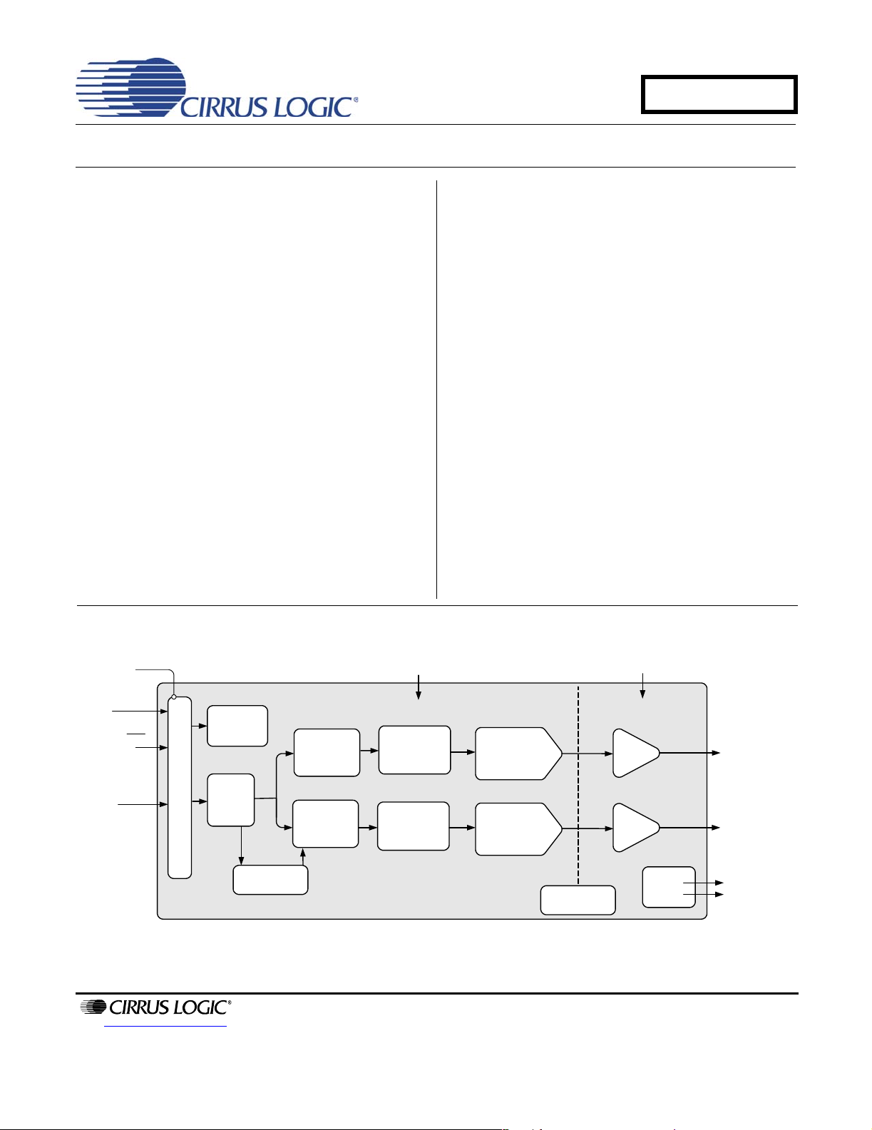
Description
The CS4352 is a complete stereo digital-to-analog system including digital interpolation, fifth-order multi-bit
delta-sigma digital-to-analog conversion, digital de-emphasis, analog filtering, and on-chip 2 Vrms line-level
driver. The advantages of this architecture include ideal
differential linearity, no distortion mechanisms due to resistor matching errors, no linearity drift over time and
temperature, high tolerance to clock jitter, and a minimal
set of external components.
The CS4352 is available in a 20-pin TSSOP package in
both Commercial grade (-40°C to +85°C) and Automotive grade (-40°C to +105°C). The CDB4352 Customer
Demonstration Board is also available for device evaluation and implementation suggestions. Please see
“Ordering Information” on page 20 for complete details.
These features are ideal for cost-sensitive, 2-channel
audio systems including video game consoles, DVD
players, A/V receivers, set-top boxes, digital TVs and
DVD Recorders, mini-component systems, and mixing
consoles.
1.5 V to 3.3 V
Hardware Control
Reset
Serial Audio Input
http://www.cirrus.com
Level Translator
Hardware
Configuration
PCM
Serial
Interface
Auto Speed Mode
Detect
Interpolation
Filter
Interpolation
Filter
3.3 V
Multibit
∆Σ Modulator
Multibit
∆Σ Modulator
Copyright © Cirrus Logic, Inc. 2007
(All Rights Reserved)
DAC
DAC
Internal Voltage
Reference
9 V to 12 V
Amp
+
Filter
Amp
+
Filter
External
Mute
Control
2 Vrms Line Level
Left Channel
Output
2 Vrms Line Level
Right Channel
Output
Left and Right
Mute Controls
JUN '07
DS684F2
Page 2

TABLE OF CONTENTS
1. PIN DESCRIPTIONS ............................................................................................................................. 3
2. CHARACTERISTICS AND SPECIFICATIONS ...................................................................................... 4
RECOMMENDED OPERATING CONDITIONS .................................................................................... 4
ABSOLUTE MAXIMUM RATINGS ........................................................................................................ 4
DAC ANALOG CHARACTERISTICS - COMMERCIAL (-CZZ) ............................................................. 5
DAC ANALOG CHARACTERISTICS - AUTOMOTIVE (-DZZ) .............................................................. 6
COMBINED INTERPOLATION & ON-CHIP ANALOG FILTER RESPONSE ........................................ 7
SWITCHING SPECIFICATIONS - SERIAL AUDIO INTERFACE ................................................... 8
DIGITAL CHARACTERISTICS ...................................................................... ... ... .... ... ... ... ..................... 9
POWER AND THERMAL CHARACTERISTICS ................................................................................... 9
3. TYPICAL CONNECTION DIAGRAM ................................................................................................... 10
4. APPLICATIONS ................................................................................................................................... 11
4.6.1 Capacitor Placement ............................................................................................................. 13
4.7.1 Power-Up .................... ... .... ... ... ... ....................................... ... ... .... ... ...................................... 14
4.7.2 Power-Down ................................ ... .... ... ... ... .... ... ... ....................................... ... ... ... ................ 14
4.7.3 Discharge Time .............. ....................................................................................................... 14
5. DIGITAL FILTER RESPONSE PLOTS ......................................................................................... 16
6. PARAMETER DEFINITIONS ................................................................................................................ 18
7. PACKAGE DIMENSIONS ................................................................................................................... 19
8. ORDERING INFORMATION ............................................................................................................... 20
9. REVISION HISTORY ............................................................................................................................ 20
CS4352
LIST OF FIGURES
Figure 1.Serial Input Timing ...... ... ... ... .... ... ... ... ... .... ... .......................................... ... ... .................................. 8
Figure 2.Typical Connection Diagram ....................................................................................................... 10
Figure 3.I²S, up to 24-Bit Data .................................................................................................................. 12
Figure 4.Right-Justified Data ........................... ... .... ... ... ... .... ... ... ... .... ... ... ................................................... 12
Figure 5.Left-Justified up to 24-Bit Data .................................................................................................... 12
Figure 6.De-Emphasis Curve .................................... ... ... .... ... ... ... .... ......................................................... 13
Figure 7.Single-Speed Stopband Rejection .............................................................................................. 16
Figure 8.Single-Speed Transition Band .................................................................................................... 16
Figure 9.Single-Speed Transition Band (detail) ........................................................................................ 16
Figure 10.Single-Speed Passband Ripple ............. ... ... ... .... ... ... ... .... ... .......................................... ... ......... 16
Figure 11.Double-Speed Stopband Rejection .............................. .... ... ... ... ... .... ... ... ... .... ... ... ... ... .... ... ......... 16
Figure 12.Double-Speed Transition Band ................................................................................................. 16
Figure 13.Double-Speed Transition Band (detail) ..................................................................................... 17
Figure 14.Double-Speed Passband Ripple .................................. .......................................... ................... 17
Figure 15.Quad-Speed Stopband Rejection ............................................................................................. 17
Figure 16.Quad-Speed Transition Band ............................. ... ... ... .... ... ... ... ... .... ... ... ... .... ... ... ... ... .... ... ......... 17
Figure 17.Quad-Speed Transition Band (detail) ................................. ... ... ... .... ... ... ... .... ... ... ... ... .... ... ......... 17
Figure 18.Quad-Speed Passband Ripple ................................................................................................. 17
LIST OF TABLES
Table 1. CS4352 Auto-Detect ................................................................................................................... 11
Table 2. Single-Speed Mode Standard Frequencies ................................................................................11
Table 3. Double-Speed Mode Standard Frequencies ............................................................................... 11
Table 4. Quad-Speed Mode Standard Frequencies ................................................................................. 11
Table 5. Digital Interface Format ............................................................................................................... 12
2 DS684F2
Page 3
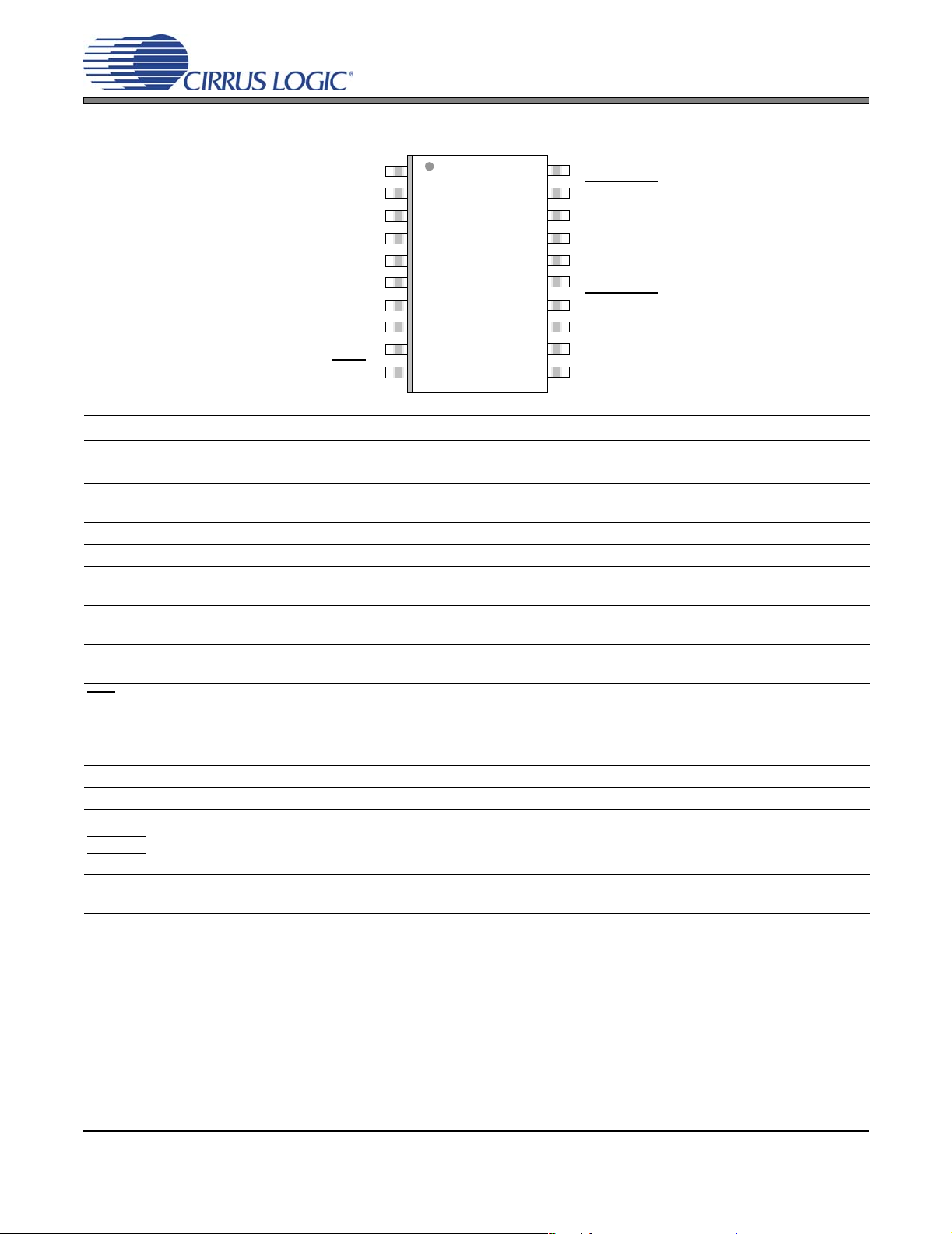
1. PIN DESCRIPTIONS
CS4352
SDIN VL
SCLK AMUTEC
LRCK AOUTA
MCLK VA_H
VD GND
GND AOUTB
DIF1 BMUTEC
DIF0 VQ
DEM VBIAS
RST
1
2
3
4
5
6
7
8
9
10
20
19
18
17
16
15
14
13
12
11
VA
Pin Name Pin # Pin Description
SDIN 1 Serial Audio Data Input (Input) - Input for two’s complement serial audio data.
SCLK 2 Serial Clock (Input) - Serial clock for the serial audio interface.
LRCK 3
MCLK 4 Master Clock (Input) - Clock source for the delta-sigma modulator and digital filters.
VD 5 Digital Power (Input) - Positive power supply for the digital section.
GND
DIF0
DIF1
DEM 9
RST
VA 11 Low Voltage Analog Power (Input) - Positive power supply for the analog section.
VBIAS 12 Positive Voltage Reference (Output) - Positive reference voltage for the internal DAC.
VQ 13 Quiescent Voltage (Output) - Filter connection for internal quiescent voltage.
VA_H 17 High Voltage Analog Power (Input) - Positive power supply for the analog section.
VL 20 Serial Audio Interface Power (Input) - Positive power for the serial audio interface
BMUTEC
AMUTEC
AOUTB
AOUTA
Left / Right Clock (Input) - Determines which channel, Left or Right, is currently active on the serial
audio data line.
6
Ground (Input) - Ground reference.
16
87Digital Interface Format (Input) - Defines the required relationship between the Left/Right Clock, Serial
Clock, and Serial Audio Data.
De-emphasis (Input) - Selects the standard 15 µs/50 µs digital de-emphasis filter response for 44.1 kHz
sample rates
Reset (Input) - Powers down the device and resets all internal registers to their default settings when
10
enabled.
14
Mute Control (Output) - Control signal for optional mute circuit.
19
1518Analog Outputs (Output) - The full-scale analog line output level is specified in the Analog Characteris-
tics table.
DS684F2 3
Page 4
CS4352
2. CHARACTERISTICS AND SPECIFICATIONS
RECOMMENDED OPERATING CONDITIONS
(GND = 0 V; all voltages with respect to ground.)
Parameters Symbol Min Typ Max Units
DC Power Supply High Voltage Analog power
Low Voltage Analog power
Digital power
Interface power
Ambient Operating Temperature (power applied) -CZZ
-DZZ
V
A_H
V
V
V
T
8.40
A
D
L
A
3.13
3.13
1.43
-40
-40
9
3.3
3.3
1.5
12.6
3.47
3.47
3.47
-
-
+85
+105
V
V
V
V
°C
°C
ABSOLUTE MAXIMUM RATINGS
(GND = 0 V; all voltages with respect to ground.)
Parameters Symbol Min Max Units
DC Power Supply High Voltage Analog power
Low Voltage Analog power
Digital power
Interface power
Input Current, Any Pin Except Supplies I
Digital Input Voltage Digital Interface V
Ambient Operating Temperature (power applied) T
Storage Temperature T
Operation at or beyond these limits may result in permanent damage to the device. Normal operation is not guaranteed at these extremes.
V
A_H
V
V
V
in
IN-L
stg
-0.3
A
D
L
A
-0.3
-0.3
-0.3
-±10mA
-0.3 VL+ 0.4 V
-55 +125 °C
-65 +150 °C
14.0
3.63
3.63
3.63
V
V
V
V
4 DS684F2
Page 5
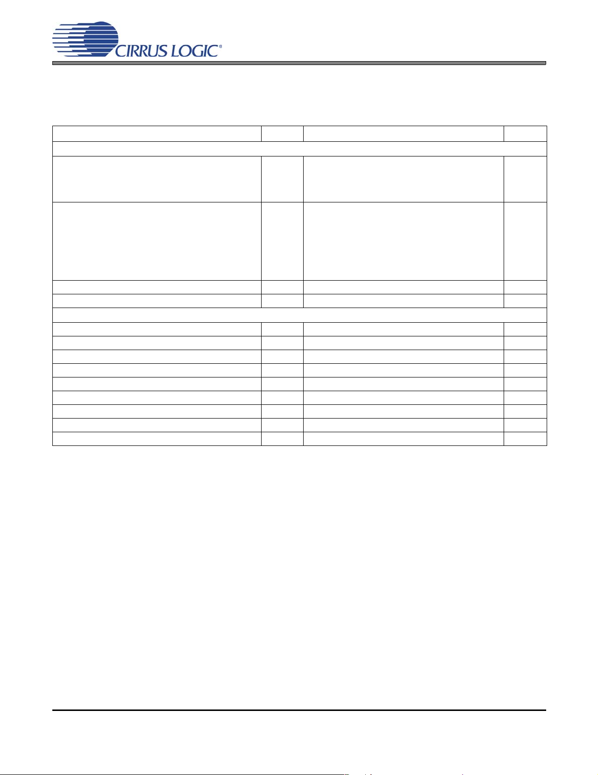
CS4352
DAC ANALOG CHARACTERISTICS - COMMERCIAL (-CZZ)
Test conditions (unless otherwise specified): TA = 25 °C, VA_H = 9 V, VA = 3.3 V, VD = 3.3 V GND = 0 V; VBIAS+
and VQ capacitors as shown in Figure 2 on page 10; input test signal is a 997 Hz sine wave at 0 dBFS; measure-
ment bandwidth 10 Hz to 20 kHz.
Parameter Symbol Min Typ Max Unit
All Speed Modes Fs = 48, 96, and 192 kHz
Dynamic Range (Note 1) 24-bit A-Weighted
unweighted
16-bit A-Weighted
unweighted
Total Harmonic Distortion + Noise (Note 1)
24-bit 0 dB
-20 dB
-60 dB
16-bit 0 dB
-20 dB
-60 dB
Idle Channel Noise / Signal-to-noise ratio (A-wt) - 106 - dB
Interchannel Isolation ( 1 kHz) - 99 - dB
THD+N
Analog Output - All Modes
Full Scale Output Voltage 1.84 2.00 2.11 Vrms
Common Mode Voltage V
Max Current draw from an AOUT pin I
Max Current draw from VQ I
Interchannel Gain Mismatch - 0.1 - dB
Gain Drift - 100 - ppm/°C
Output Impedance Z
AC-Load Resistance R
Load Capacitance C
Q
OUTmax
Qmax
OUT
L
L
100
97
-
-
-
-
-
-
-
-
-
-4-Vdc
- 575 - µA
-1-µA
-50-Ω
5--kΩ
--100pF
106
103
98
95
-93
-83
-43
-93
-75
-35
-
-
-
-
-89
-77
-37
-
-
-
dB
dB
dB
dB
dB
dB
dB
dB
dB
dB
Notes:
1. One-half LSB of triangular PDF dither is added to data.
DS684F2 5
Page 6

CS4352
DAC ANALOG CHARACTERISTICS - AUTOMOTIVE (-DZZ)
Test conditions (unless otherwise specified): TA = -40°C to 85°C, VA_H = 9 V, VA = 3.3 V, VD = 3.3 V GND = 0 V;
VBIAS+ and VQ capacitors as shown in Figure 2 on page 10; input test signal is a 997 Hz sine wave at 0 dBFS;
measurement bandwidth 10 Hz to 20 kHz.
Parameter Symbol Min Typ Max Unit
All Speed Modes Fs = 48, 96, and 192 kHz
Dynamic Range (Note 2) 24-bit A-Weighted
unweighted
16-bit A-Weighted
unweighted
Total Harmonic Distortion + Noise (Note 2)
24-bit 0 dB
-20 dB
-60 dB
16-bit 0 dB
-20 dB
-60 dB
Idle Channel Noise / Signal-to-noise ratio (A-wt) - 106 - dB
Interchannel Isolation (1 kHz) - 99 - dB
THD+N
Analog Output - All Modes
Full Scale Output Voltage 1.81 2.00 2.17 Vrms
Common Mode Voltage V
Max Current draw from an AOUT pin I
Max Current draw from VQ I
Interchannel Gain Mismatch - 0.1 - dB
Gain Drift - 100 - ppm/°C
Output Impedance Z
AC-Load Resistance R
Load Capacitance C
Q
OUTmax
Qmax
OUT
L
L
96
93
-
-
-
-
-
-
-
-
-
-4-Vdc
-575-µA
-1-µA
-50-Ω
5--kΩ
- - 100 pF
106
103
98
95
-93
-83
-43
-93
-75
-35
-
-
-
-
-89
-73
-33
-
-
-
dB
dB
dB
dB
dB
dB
dB
dB
dB
dB
Notes:
2. One-half LSB of triangular PDF dither is added to data.
6 DS684F2
Page 7

CS4352
COMBINED INTERPOLATION & ON-CHIP ANALOG FILTER RESPONSE
(The filter characteristics have been normalized to the sample rate (Fs) and can be referenced to the desired sample rate by multiplying the given characteristic by Fs. Amplitude vs. frequency plots of the data in the table below
are available in “Digital Filter Response Plots” on page 16.)
Parameter Min Typ Max Unit
Combined Digital and On-chip Analog Filter Response - Single-Speed Mode - 48 kHz
Passband (Note 3) to -0.01 dB corner
to -3 dB corner
Frequency Response 10 Hz to 20 kHz -0.01 - +0.01 dB
StopBand 0.547 - - Fs
StopBand Attenuation (Note 4) 102 - - dB
Total Group Delay (Fs = Output Sample Rate) - 9.4/Fs - s
Intra-channel Phase Deviation - - ±0.56/Fs s
Inter-channel Phase Deviation - - 0 s
De-emphasis Error (Note 5)(Relative to 1 kHz) Fs = 44.1 kHz - - ±0.14 dB
Combined Digital and On-chip Analog Filter Response - Double-Speed Mode - 96 kHz
Passband (Note 3) to -0.01 dB corner
to -3 dB corner
Frequency Response 10 Hz to 20 kHz -0.01 - 0.01 dB
StopBand .583 - - Fs
StopBand Attenuation (Note 4) 80 - - dB
Total Group Delay (Fs = Output Sample Rate) - 4.6/Fs - s
Intra-channel Phase Deviation - - ±0.03/Fs s
Inter-channel Phase Deviation - - 0 s
Combined Digital and On-chip Analog Filter Response - Quad-Speed Mode - 192 kHz
Passband (Note 3) to -0.01 dB corner
to -3 dB corner
Frequency Response 10 Hz to 20 kHz -0.01 - 0.01 dB
StopBand .635 - - Fs
StopBand Attenuation (Note 4) 90 - - dB
Total Group Delay (Fs = Output Sample Rate) - 4.7/Fs - s
Intra-channel Phase Deviation - - ±0.01/Fs s
Inter-channel Phase Deviation - - 0 s
0
0
0
0
0
0
-
-
-
-
-
-
.454
.499
.430
.499
.105
.490
Fs
Fs
Fs
Fs
Fs
Fs
Notes:
3. Response is clock-dependent and will scale with Fs.
4. For Single-Speed Mode, the Measurement Bandwidth is from stopband to 3 Fs.
For Double-Speed Mode, the Measurement Bandwidth is from stopband to 3 Fs.
For Quad-Speed Mode, the Measurement Bandwidth is from stopband to 1.34 Fs.
5. De-emphasis is available only in Single-Speed Mode.
DS684F2 7
Page 8

CS4352
SWITCHING SPECIFICATIONS - SERIAL AUDIO INTERFACE
Parameters Symbol Min Max Units
MCLK Frequency 1.024 48.0 MHz
MCLK Duty Cycle 45 55 %
Input Sample Rate (Auto selection) Single-Speed Mode
Double-Speed Mode
Quad-Speed Mode
LRCK Duty Cycle 40 60 %
SCLK Pulse Width Low t
SCLK Pulse Width High t
SCLK Period Single-Speed Mode t
Double-Speed Mode t
Quad-Speed Mode t
Fs
Fs
Fs
sclkl
sclkh
sclkw
sclkw
sclkw
4
84
170
54
108
216
20 - ns
20 - ns
1
--------------------- 128()Fs
1
-----------------64()Fs
2
-----------------
MCLK
--
--
--
kHz
kHz
kHz
SCLK rising to LRCK edge delay t
SCLK rising to LRCK edge setup time t
SDIN valid to SCLK rising setup time t
SCLK rising to SDIN hold time t
LRCK
t
t
slrd
slrs
t
sclkl
SCLK
t
sdlrs
t
sdh
SDATA
Figure 1. Serial Input Timing
slrd
slrs
sdlrs
sdh
t
sclkh
20 - ns
20 - ns
20 - ns
20 - ns
8 DS684F2
Page 9

CS4352
DIGITAL CHARACTERISTICS
Parameters Symbol Min Typ Max Units
High-Level Input Voltage VL = 3.3 V
= 2.5 V
V
L
= 1.5 V
V
L
Low-Level Input Voltage VL = 3.3 V
= 2.5 V
V
L
= 1.5 V
V
L
Input Leakage Current I
V
IH
V
IH
V
IH
V
IL
V
IL
V
IL
in
Input Capacitance - 8 - pF
Maximum MUTEC Drive Current - 2 - mA
MUTEC High-Level Output Voltage V
MUTEC Low-Level Output Voltage V
OH
OL
2.0
1.7
1.05
-
-
-
-
-
-
-
-
-
-
-
-
0.8
0.7
0.38
--±10µA
-VA_H- V
-0- V
V
V
V
V
V
V
POWER AND THERMAL CHARACTERISTICS
Parameters Symbol Min Typ Max Units
Power Supplies
Power Supply Current normal operation, V
(Note 6) V
Interface current V
power-down state, all supplies (Note 7)
Power Dissipation (all supplies) (Note 6)
VA_H = 12V normal operation
power-down (Note 7)
VA_H = 9V normal operation
power-down (Note 7)
Power Supply Rejection Ratio (Note 8) (1 kHz)
Notes:
6. Current consumption increases with increasing FS and increasing MCLK. Typ and Max values are
based on highest FS and highest MCLK. Variance between speed modes is small.
7. Power down mode is defined as RST
inputs have a weak pull-down which is only present during reset. Opposing this pull-down will slightly
increase the power-down current (pull-down is equivalent to a 50 kΩ resistor per pin).
8. Valid with the recommended capacitor values on VQ and V
gram in Section 3.
= 12 V
A_H
= 9 V
A_H
= 3.3 V
V
A
VD= 3.3 V
= 3.3 V
L
(60 Hz)
pin = Low with all clock and data lines held static low. All digital
I
A_H
I
A_H
I
A
I
D
I
L
I
pd
PSRR -
as shown in the typical connection dia-
BIAS
-
-
-
-
-
-
-
-
-
-
-
12
10
3
12
0.02
380
121
1
91
1
60
60
21
16
4
16
0.09
-
158
-
122
-
-
-
mA
mA
mA
mA
mA
µA
mW
mW
mW
mW
dB
dB
DS684F2 9
Page 10

3. TYPICAL CONNECTION DIAGRAM
CS4352
+3.3 V *
*Remove this supply if
optional resistor is present.
The decoupling caps should
remain.
+1.5 V to VD
Source
Mode
Configuration
10 µF
Digital
Audio
0.1 µF
0.1 µF
4
3
2
1
20
10
7
8
9
5 11
VD
MCLK
LRCK
SCLK
SDIN
VL
CS4352
RST
DIF1
DIF0
DEM
D
N
G
6
5.1Ω∗
*Optional
AMUTEC
BMUTEC
15
VBIAS+
VA_H
AOUTA
AOUTB
ND
G
VA
VQ
0.1 µF
12
17
19
18
14
15
13
0.1 µF
3.3 µF
3.3 µF
3.3 µF
10 k
10 k
10 µF
560 Ω
Ω
560 Ω
Ω
10 µF
3.3 µF
+9 V to +12 V
2.2 nF*
2.2 nF*
+3.3 V
Optional
Mute
Circuit
Optional
Mute
Circuit
*Shown value is
for Fc=130 kHz
Left Out
Right Out
Figure 2. Typical Connection Diagram
10 DS684F2
Page 11

4. APPLICATIONS
4.1 Sample Rate Range/Operational Mode Detect
The device operates in one of three operational modes. The allowed sample rate range in each mode is
auto-detected.
The CS4352 will auto-detect the correct mode when the input sample rate (Fs), defined by the LRCK frequency, falls within one of the ranges illustrated in Table 1. Sample rates outside the specified range for
each mode are not supported.
Input Sample Rate (FS) Mode
4 kHz - 54 kHz Single-Speed Mode
84 kHz - 108 kHz Double-Speed Mode
170 kHz - 216 kHz Quad-Speed Mode
Table 1. CS4352 Auto-Detect
4.2 System Clocking
The device requires external generation of the master (MCLK), left/right (LRCK) and serial (SCLK) clocks.
The left/right clock, defined also as the input sample rate (F
MCLK according to specified ratios. The specified ratios of MCLK to LRCK, along with several standard audio sample rates and the required MCLK frequency, are illustrated in Tables 2-4.
CS4352
), must be synchronously derived from the
s
Refer to Section 4.3 for the required SCLK timing associated with the se lected Digital Interface Format an d
to “Switching Specifications - Serial Audio Interface” o n page 8 for the maximum allowed clock frequencies.
Sample Rate
(kHz)
32 8.1920 12.2880 16.3840 24.5760 32.7680
44.1 11.2896 16.9344 22.5792 33.8688 45.1584
48 12.2880 18.4320 24.5760 36.8640 49.1520
256x 384x 512x 768x 1024x
T able 2. Single-Speed Mode Standard Frequencies
Sample Rate
(kHz)
88.2 11.2896 16.9344 22.5792 33.8688 45.1584
96 12.2880 18.4320 24.5760 36.8640 49.1520
128x 192x 256x 384x 512x
Table 3. Double-Speed Mode Standard Frequencies
Sample Rate
(kHz)
176.4 22.5792 33.8688 45.1584
192 24.5760 36.8640 49.1520
Table 4. Quad-Speed Mode Standard Frequencies
128x 192x 256x
MCLK (MHz)
MCLK (MHz)
MCLK (MHz)
DS684F2 11
Page 12

4.3 Digital Interface Format
The device will accept audio samples in 1 of 4 digital interface formats, as illustrated in Table 5.
The desired format is selected via the DIF1 and DIF0 pins. For an illustration of the required relationship
between the LRCK, SCLK and SDIN, see Figures 3-5. For all formats, SDIN is valid on the rising edge of
SCLK. Also, SCLK must have at least 32 cycles per LRCK period in format 2 an d 48 cycles per LRCK period
in format 3.
For more information about serial audio formats, refer to Cirrus Logic Application Note AN282: The 2-Chan-
nel Serial Audio Interface: A Tutorial, available at www.cirrus.com.
DIF1 DIF0 DESCRIPTION FORMAT FIGURE
00
01
10
11
I²S, up to 24-bit Data
Right-Justified, 24-bit Data
Left-Justified, up to 24-bit Data
Right-Justified, 16-bit Data
CS4352
0 3
1 4
2 5
3 4
Table 5. Digital Interface Format
LRCK
SCLK
SDIN +3 +2 +1+5 +4
LRCK
SCLK
MSB
SDIN
MSB
-1 -2 -3 -4 -5
Left Channel
Left C hannel
+1 +2 +3 +4
LRCK
SCLK
SDIN +3 +2 +1+5 +4
MSB
-1 -2 -3 -4 -5
Left C hannel
Right Channel
LSB
MSB
-1 -2 -3 -4
+3 +2 +1+5 +4
LSB
Figure 3. I²S, up to 24-Bit Data
Right Channel
+5
-6 -5 -4 -3 -2 -1-7
LSBMSB
MSB
+1 +2 +3 +4
+5
-6 -5 -4 -3 -2 -1-7
LSB
Figure 4. Right-Justified Data
Right Channel
LSB
MSB
-1 -2 -3 -4
+3 +2 +1+5 +4
LSB
Figure 5. Left-Justified up to 24-Bit Data
12 DS684F2
Page 13

4.4 De-Emphasis Control
The device includes on-chip digital de-emphasis. Figure 6 shows the de-emphasis curve for Fs equal to
44.1 kHz. The frequency response of the de-emphasis curve scales with changes in sample rate, Fs. The
De-emphasis error will increase for sample rates other than 44.1 kHz
When pulled to VL, the DEM pin activates the 44.1 kHz de-emphasis filter. When pulled to GND, the DEM
pin turns off the de-emphasis filter.
-10dB
CS4352
Gain
dB
T1=50 µs
0dB
T2 = 15 µs
F1 F2
3.183 kHz 10.61 kHz
Figure 6. De-Emphasis Curve
Note: De-emphasis is only available in Single-Speed Mode.
4.5 Recommended Power-Up Sequence
1. Hold RST low until the power supplies and configuration pins are stable, and the master and left/right
clocks are locked to the appropriate frequencies, as discussed in Section 4.2. In this state, VQ will remain low and VBIAS will be connected to VA.
2. Bring RST
high. The device will remain in a low power state with VQ low and will initiate the power-up
sequence after approximately 512 LRCK cycles in Single-Speed Mode (1024 LRCK cycles in DoubleSpeed Mode, and 2048 LRCK cycles in Quad-Speed Mode).
4.6 Grounding and Power Supply Arrangements
As with any high-resolution converter, the CS4352 requires careful attention to power supply and grounding
arrangements if its potential performance is to be realized. Figure 2 shows the recommended power arrangements, with VA_H, VA, VD, and VL connected to clean supplies. If the ground planes are split between
digital ground and analog ground, the GND pins of the CS4352 should be connected to the analog ground
plane.
All signals, especially clocks, should be kept away from the VBIAS and VQ pins in order to avoid unwanted
coupling into the DAC.
Frequency
4.6.1 Capacitor Placement
Decoupling capacitors should be placed as close to the DAC as possible, with the low-value ceramic capacitor being the closest. To further minimize impedance, these capacitors should be located on the same
layer as the DAC. If desired, all supply pins may be connected to the same supply, but a decoupling capacitor should still be placed on each supply pin.
Note: All decoupling capacitors should be referenced to analog ground.
The CDB4352 evaluation board demonstrates the optimum layout and power supply arrangements.
DS684F2 13
Page 14

4.7 Popguard Transient Control
The CS4352 uses a novel technique to minimize the effects of output transients du ring power-up and powerdown. This technology, when used with exte rnal DC-blocking capacitors in series with the audio outputs,
minimizes the audio transients commonly produced by single-ended, single-supp ly converte rs. It is activated inside the DAC when the RST
the appropriate DC-blocking capacitors.
pin is toggled and requires no other extern al control, aside from choosing
4.7.1 Power-Up
When the device is initially powered-up, the audio outputs, AOUTA and AOUTB, are clamped to GND.
Following a delay of approximately 1000 sample periods, each output begins to ramp toward the quiescent voltage. Approximately 10,000 LRCK cycles later, the outputs reach V
This gradual voltage ramping allows time for the external DC-blocking capacitors to charge to the quiescent voltage, minimizing audible power-up transients.
4.7.2 Power-Down
To prevent audible transients at power-down, the device must first enter its po wer- down state. Whe n th is
occurs, audio output ceases, and the internal output buffer s are disconnected fr om AOUTA and AOUTB.
In their place, a soft-start current sink is substituted that allows the DC-blocking capacitors to slowly discharge. Once this charge is dissipated, the power to the device may be turned off, and the system is ready
for the next power-on.
CS4352
and audio output begins.
Q
4.7.3 Discharge Time
To prevent an audio transient at the next power-on, the DC-blocking capacitors must fully discharge before turning on the power or exiting the power-down state . If full discharg e does not occu r, a transient will
occur when the audio outputs are initially clamped to GND. The time that the device must remain in the
power-down state is related to the value of the DC-blocking ca pacitance and the output load. For example,
with a 3.3 µF capacitor, the minimum power-down time will be approximately 0.4 seconds.
4.8 Mute Control
The Mute Control pins go active during power-up initialization, reset, muting, or if the MCLK to LRCK ratio
is incorrect. These pins are intended to be used as control for external mute circuits to prevent the clicks
and pops that can occur in any single-ended, single-supply system.
Use of the Mute Control function is not mandatory but recommended for designs requiring the absolute minimum in extraneous clicks and pops. Also, use of the Mute Control function can enable the system designer
to achieve idle channel noise/signal-to-noise ratios which are only limited by the external mute circuit.
Please see the CDB4352 data sheet for a suggested mute circuit for dual-supply systems. Alternately, the
FET muting circuit from the CS4351 data sheet may be used as well. This FET circuit must be placed in
series after the RC filter; otherwise noise may occur during muting conditions. Further ESD protection will
need to be taken into consideration for the FET used.
14 DS684F2
Page 15

4.9 Initialization and Power-Down Sequence Diagram
USER: Apply Power
CS4352
Power-Down State
VQ and outputs low
USER: Apply MCLK, SCLK, LRCK,
and release RST
VQ and outputs ramp up
USER: Apply MCLK, SCLK, and LRCK
Wait State
VQ and outputs
ramp down
USER: Apply RST
USER: Remove
LRCK or MCLK
MCLK/LRCK Ratio Detection
USER: change
MCLK/LRCK ratio
Analog Output
is Generated
DS684F2 15
Page 16

5. DIGITAL FILTER RESPONSE PLOTS
CS4352
0
−20
−40
−60
Amplitude (dB)
−80
−100
−120
0.4 0.5 0.6 0.7 0.8 0.9 1
Frequency(normalized to Fs)
0
−20
−40
−60
Amplitude (dB)
−80
−100
−120
0.4 0.42 0.44 0.46 0.48 0.5 0.52 0.54 0.56 0.58 0.6
Frequency(normalized to Fs)
Figure 7. Single-Speed Stopband Rejection Figure 8. Single-Speed Transition Band
0
−1
−2
−3
−4
−5
Amplitude (dB)
−6
−7
−8
−9
−10
0.45 0.46 0.47 0.48 0.49 0.5 0.51 0.52 0.53 0.54 0.55
Frequency(normalized to Fs)
0.02
0.015
0.01
0.005
0
Amplitude (dB)
−0.005
−0.01
−0.015
−0.02
0 0.05 0.1 0.15 0.2 0.25 0.3 0.35 0.4 0.45 0.5
Frequency(normalized to Fs)
Figure 9. Single-Speed Transition Band (detail) Figure 10. Single-Speed Passband Ripple
0
20
40
60
Amplitude (dB)
80
100
120
0.4 0.5 0.6 0.7 0.8 0.9 1
Frequency(normalized to Fs)
0
20
40
60
Amplitude (dB)
80
100
120
0.4 0.42 0.44 0.46 0.48 0.5 0.52 0.54 0.56 0.58 0.6
Frequency(normalized to Fs)
Figure 11. Double-Speed Stopband Rejection Figure 12. Double-Speed Transition Band
16 DS684F2
Page 17

CS4352
0
1
2
3
4
5
Amplitude (dB)
6
7
8
9
10
0.45 0.46 0.47 0.48 0.49 0.5 0.51 0.52 0.53 0.54 0.55
Frequency(normalized to Fs)
0.02
0.015
0.01
0.005
0
Amplitude (dB)
0.005
0.01
0.015
0.02
0 0.05 0.1 0.15 0.2 0.25 0.3 0.35 0.4 0.45 0.5
Frequency(normalized to Fs)
Figure 13. Double-Speed Transition Band (detail) Figure 14. Double-Speed Passband Ripple
0
20
40
60
Amplitude (dB)
80
0
20
40
60
Amplitude (dB)
80
100
120
0.2 0.3 0.4 0.5 0.6 0.7 0.8 0.9 1
Frequency(normalized to Fs)
100
120
0.2 0.3 0.4 0.5 0.6 0.7 0.8
Frequency(normalized to Fs)
Figure 15. Quad-Speed Stopband Rejection Figure 16. Quad-Speed Transition Band
0
1
2
3
4
5
Amplitude (dB)
6
7
8
9
10
0.45 0.46 0.47 0.48 0.49 0.5 0.51 0.52 0.53 0.54 0.55
Frequency(normalized to Fs)
0.2
0.15
0.1
0.05
0
Amplitude (dB)
0.05
0.1
0.15
0.2
0 0.05 0.1 0.15 0.2 0.25
Frequency(normalized to Fs)
Figure 17. Quad-Speed Transition Band (detail) Figure 18. Quad-Speed Passband Ripple
DS684F2 17
Page 18

6. PARAMETER DEFINITIONS
Total Harmonic Distortion + Noise (THD+N)
The ratio of the rms value of the signal t o the rms su m of all other spectral components over the specified
bandwidth (typically 10 Hz to 20 kHz), including distortion components. Expressed in decibels.
Dynamic Range
The ratio of the full-scale rms value of the signal to the rms sum of all other spectral components over the
specified bandwidth. Dynamic range is a signal-to-noise measurement over the specified bandwidth made
with a -60 dBFS signal. 60 dB is then added to the resulting measurement to refer the measurement to full
scale. This technique ensures that the distortion components are be low the noise level and do not effect the
measurement. This measurement technique has been accepted by the Audio Engineering Society, AES171991, and the Electronic Industries Association of Japan, EIAJ CP-307.
Interchannel Isolation
A measure of crosstalk between the left and right channels. Measured for each channel at the converter's
output with all zeros to the input under test and a full-scale signa l applied to the other channel. Units in d ecibels.
Interchannel Gain Mismatch
The gain difference between left and right channels. Units in decibels.
CS4352
Gain Error
The deviation from the nominal full-scale analog output for a full-scale digital input.
Gain Drift
The change in gain value with temperature. Units in ppm/°C.
Intra-channel Phase Deviation
The deviation from linear phase within a given channel.
Inter-channel Phase Deviation
The difference in phase between channels.
18 DS684F2
Page 19

7. PACKAGE DIMENSIONS 20L TSSOP (4.4 mm BODY) PACKAGE DRAWING
N
CS4352
1
23
TOP VIEW
D
E
e
2
b
SIDE VIEW
A2
A1
A
SEATING
PLANE
L
1
E1
END VIEW
INCHES MILLIMETERS NOTE
DIM MIN NOM MAX MIN NOM MAX
A -- -- 0.043 -- -- 1.10
A1 0.002 0.004 0.006 0.05 -- 0.15
A2 0.03346 0.0354 0.037 0.85 0.90 0.95
b 0.00748 0.0096 0.012 0.19 0.245 0.30 2,3
D 0.252 0.256 0.259 6.40 6.50 6.60 1
E 0.248 0.2519 0.256 6.30 6.40 6.50
E1 0.169 0.1732 0.177 4.30 4.40 4.50 1
e -- -- 0.026 -- -- 0.65
L 0.020 0.024 0.028 0.50 0.60 0.70
µ
0° 4° 8° 0° 4° 8°
∝
JEDEC #: MO-153
Controlling Dimension is Millimeters.
1. “D” and “E1” are reference datums and do not included mold flash or protrusions, but do include mold
mismatch and are measured at the parting line, mold flash or protrusions shall not exceed 0.20 mm per
side.
2. Dimension “b” does not include dambar protrusion/intrusion. Allowable dambar protrusion shall be
0.13 mm total in excess of “b” dimension at maximum material condition. Dambar intrusion shall not reduce dimension “b” by more than 0.07 mm at least material condition.
3. These dimensions apply to the flat section of the lead between 0.10 and 0.25 mm from lead tips.
Parameters Symbol Min Typ Max Units
Package Thermal Resistance 20L TSSOP θ
JA
-72-°C/Watt
DS684F2 19
Page 20

CS4352
8. ORDERING INFORMATION
Product Description Package Pb-Free Grade Temp Range Container Order #
CS4352
20-pin, 192 kHz Stereo
DAC with 2 Vrms Line
Out
20-pin
TSSOP
YES
Commercial -40° to +85° C
Automotive -40° to +105° C
Rail
Tape & Reel
Rail
Tape & Reel
CS4352-CZZ
CS4352-CZZR
CS4352-DZZ
CS4352-DZZR
CDB4352 CS4352 Evaluation Board - - - - CDB4352
9. REVISION HISTORY
Release Changes
Lowered V
PP1
Updated Idle channel noise specification to A-wt.
Updated AOUT current draw specification.
Updated V
F1 Updated performance specifications and limits based on statistical data.
Added Automotive grade specifications and ordering information.
Updated Commercial grade idle channel noise specification.
F2
Lowered V
Updated power supply current specification.
Updated MCLK maximum specification.
minimum specification.
A_H
for VL=1.5V.
IL
maximum specifcation.
IL
Contacting Cirrus Logic Support
For all product questions and inquiries, contact a Cirrus Logic Sales Representative.
To find the one nearest you, go to www.cirrus.com.
IMPORTANT NOTICE
Cirrus Logic, Inc. and its subsidiaries ("Cirrus") believe that the information contained in this document is accurate and reliable. However, the information is subject
to change without not ice and is pr ovided "AS IS" witho ut warr anty of any kind (express or implied). Customers are advised to obtain the latest version of relevant
information to verify, before placing orders, that information being relied on is current and complete. All products are sold subject to the terms and conditions of sale
supplied at the time of order acknowledgment, including those pertaining to warranty, indemnification, and limitation of liability. No responsibility is assumed by Cirrus
for the use of this information, including use of this information as the basis for manufacture or sale of any items, or for infringement of patents or other rights of third
parties. This document is the property of Cirrus and by furnishing this information, Cirrus grants no license, express or implied under any patents, mask work rights,
copyrights, trademarks, trade secrets or other inte llectual property rig hts. Cirrus owns the copyrights associated with the information contained herein and gives consent for copies to be made of the information only for use within your organization with respect to Cirrus integrated circuits or other products of Cirrus. This consent
does not extend to other copying such as copying for general distribution, advertising or promotional purposes, or for creating any work for resale.
CERTAIN APPLICATIONS USING SEMICONDUCTOR PRODUCTS MAY INVOLVE POTENTIAL RISKS OF DEATH, PERSONAL INJURY, OR SEVERE PROPERTY OR ENVIRONMENTAL DAMAGE (“CRITICAL APPLICATIONS”). CIRRUS PRODUCTS ARE NOT DESIGNED, AUTHORIZED OR WARRANTED FOR USE
IN AIRCRAFT SYSTEMS, MILITARY APPLICATIONS, PRODUCTS SURGICALLY IMPLANTED INTO THE BODY, AUTOMOTIVE SAFETY OR SECURITY DEVICES, LIFE SUPPORT PRODUCTS OR OTHER CRITICAL APPLICATIONS. INCLUSION OF CIRRUS PRODUCTS IN SUCH APPLICATIONS IS UNDERSTOOD TO BE FULLY AT THE CUSTOMER’S RISK AND CIRRUS DISCLAIMS AND MAKES NO WARRANTY, EXPRESS, STATUTORY OR IMPLIED,
INCLUDING THE IMPLIED WARRANTIES OF MERCHANTABILITY AND FITNESS FOR PARTICULAR PURPOSE, WITH REGARD TO ANY CIRRUS PRODUCT
THAT IS USED IN SUCH A MANNER. IF THE CUSTOMER OR CUSTOMER’S CUSTOMER USES OR PERMITS THE USE OF CIRRUS PRODUCTS IN CRITICAL
APPLICATIONS, CUSTOMER AGREES, BY SUCH USE, T O FULLY INDEMNIF Y CIRRUS, ITS OF FICE RS, DI RECTORS, EMPLOYEES, DISTRI BUTORS AND
OTHER AGENTS FROM ANY AND ALL LIABILITY, INCLUDING ATTORNEYS’ FEES AND COSTS, THAT MAY RESULT FROM OR ARISE IN CONNECTION
WITH THESE USES.
Cirrus Logic, Cirrus, the Cirrus Logic l ogo de si gns , an d Po pgua rd ar e t r adema rk s o f Ci r ru s Lo gi c, I nc . All other brand and pr oduct names in this document may be
trademarks or service marks of their respective owners.
20 DS684F2
 Loading...