

Page 1
u
CS4351
192 kHz Stereo DAC with 2 Vrms Line Out
Features
! Multi-Bit Delta-Sigma Modulator
! 24-Bit Conversion
! Up to 192 kHz Sample Rates
! 112 dB Dynamic Range
! -100 dB THD+N
! +3.3 V, +9 to 12 V, and VL Power Supplies
! 2 Vrms Output into 5 kΩ AC Load
! Digital Volume Control with Soft Ramp
– 119 dB Attenuation
– 1/2 dB Step Size
– Zero Crossing Click-Free Transitions
! ATAPI Mixing
! Low Clock Jitter Sensitivity
! Popguard
and Pops
®
Technology for Control of Clicks
Description
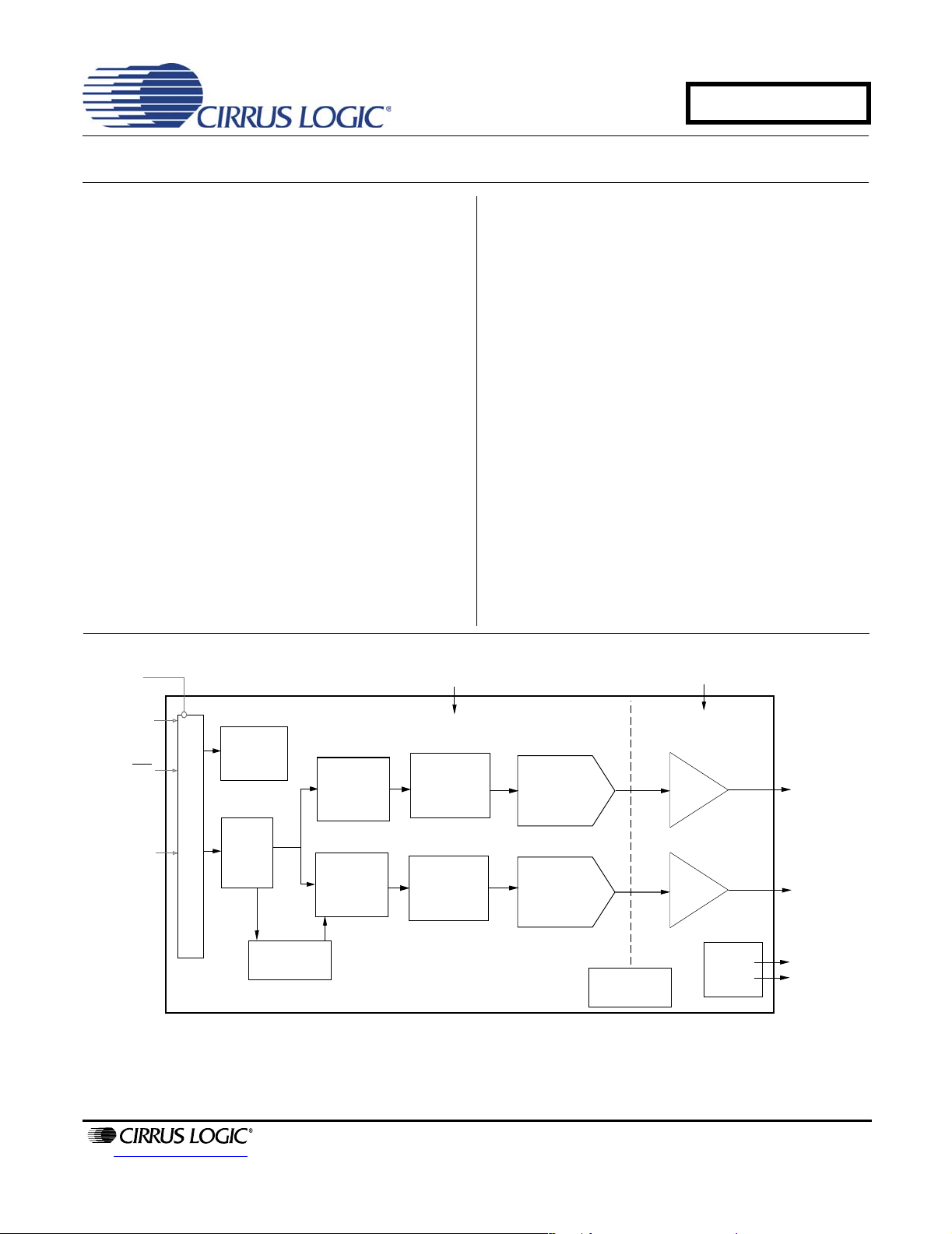
The CS4351 is a complete stereo digital-to-analog system including digital interpolation, fifth-order multi-bit
delta-sigma digital-to-analog conversion, digital de-emphasis, volume control, channel mixing, analog filtering,
and on-chip 2 Vrms line-level driver. The advantages of
this architecture include ideal differential linearity, no
distortion mechanisms due to resistor matching errors,
no linearity drift over time and tem perature, high tolerance to clock jitter, and a minimal set of external
components.
The CS4351 is available in a 20-pin TSSOP package in
both Commercial (-10°C - +70°C) and Automotive
grades (-40°C to +85°C). The CDB4351 Customer
Demonstration board is also available for device evaluation and implementation suggestions. Please see
“Ordering Information” on page 37 for complete details.
These features are ideal for cost-sensitive, 2-channel
audio systems including DVD players, A/V receivers,
set-top boxes, digital TVs and VCRs, mini-component
systems, and mixing consoles.
V to 3.3V
ware or I2C/SPI
Con t r ol Data
Reset
rial Audio Input
Level Translator
Register/Hardware
Configuration
PCM
Serial
Interfa ce
Auto Speed Mode
Detect
Interpolation
Fil ter wit h
Volume Contr ol
Interpolation
Fil ter wit h
Volume Cont r ol
3.3 V
Multibit
∆Σ Modulator
Multibit
∆Σ Modulator
DAC
DAC
Internal V oltage
Reference
9 V to 12 V
Amp
+
Filter
Amp
+
Filter
External
Mute
Contr ol
2 Vrms Line Level
Left Chann el Outp
2 Vrms Line Level
Right Channe l
Output
Left and Right
Mute Controls
http://www.cirrus.com
Copyright © Cirrus Logic, Inc. 2005
(All Rights Reserved)
DECEMBER '05
DS566F1
Page 2

TABLE OF CONTENTS
1. PIN DESCRIPTION ............................. ... ... ....................................... ... ... .... ... ... ... .... ... ... ........................ 5
2. CHARACTERISTICS AND SPECIFICATIONS ..................................................................................... 6
SPECIFIED OPERATING CONDITIONS.............................................................................................. 6
ABSOLUTE MAXIMUM RATINGS........................................................................................................6
DAC ANALOG CHARACTERISTICS .................................................................................................... 7
COMBINED INTERPOLATION & ON-CHIP ANALOG FILTER RESPONSE .......................................8
COMBINED INTERPOLATION & ON-CHIP ANALOG FILTER RESPONSE .......................................9
SWITCHING SPECIFICATIONS - SERIAL AUDIO INTERFACE ...................................................... 10
SWITCHING CHARACTERISTICS - CONTROL PORT - I²C
SWITCHING CHARACTERISTICS - CONTROL PORT - SPI™ FORMAT......................................... 12
DIGITAL CHARACTERISTICS............................... ... .... ... ... .......................................... ... ... ................ 13
POWER AND THERMAL CHARACTERISTICS ................................................................................. 13
3. TYPICAL CONNECTION DIAGRAM ........... .... ... ... ... .... ... ... .......................................... ... ... ................ 14
4. APPLICATIONS .................................................................................................................................. 15
4.1 Sample Rate Range/Operational Mode Detect ................................... ......................................... 15
4.1.1 Auto-Detect Enabled ........................................................................................................ 15
4.1.2 Auto-Detect Disabled ....................................................................................................... 15
4.2 System Clocking ........................................................................................................................... 15
4.3 Digital Interface Format ................................................................................................................ 16
4.3.1 Stand-Alone Mode ........................................................................................................... 16
4.3.2 Control Port Mode ........................................................................................................... 16
4.4 De-Emphasis Control ................................................................................................................... 17
4.4.1 Stand-Alone Mode ........................................................................................................... 18
4.4.2 Control Port Mode ............................................................................................................ 18
4.5 Recommended Power-Up Sequence ........................................................................................... 18
4.5.1 Stand-Alone Mode ........................................................................................................... 18
4.5.2 Control Port Mode ............................................................................................................ 18
4.6 Popguard
4.6.1 Power-Up ......................................................................................................................... 18
4.6.2 Power-Down .................................................................................................................... 19
4.6.3 Discharge Time ................................................................................................................ 19
4.7 Mute Control ................................................................................................................................. 19
4.8 Grounding and Power Supply Arrangements ............................................................................... 19
4.8.1 Capacitor Placement ........................................................................................................ 19
4.9 Control Port Interface ................................................................................................................... 20
4.9.1 MAP Auto Increment ........................................................................................................ 20
4.9.2 I²C Mode .......................................................................................................................... 20
4.9.3 SPI Mode ......................................................................................................................... 21
4.10 Memory Address Pointer (MAP) .................... ... .... ... ... ... .... ... ... ... ... .... ... ... ... ................................ 22
4.10.1 INCR (Auto Map Increment Enable) .............................................................................. 22
4.10.2 MAP (Memory Address Pointer) .................................................................................... 22
5. REGISTER QUICK REFERENCE .......................................... .... ... ... ... ... .... ... ... ................................... 23
6. REGISTER DESCRIPTION .......... .... .......................................... ... ... ................................................... 24
6.1 Chip ID - Register 01h .................................................................................................................. 24
6.2 Mode Control 1 - Register 02h ..................................................................................................... 24
6.2.1 Digital Interface Format (DIF2:0) Bits 6-4 ........................................................................ 24
6.2.2 De-Emphasis Control (DEM1:0) Bits 3-2. ........................................................................ 24
6.2.3 Functional Mode (FM) Bits 1-0 ............................ .... ... ... ... ... .... ... ... ... .... ... ... ... ... .... ... ... ... ... 25
6.3 Volume Mixing and Inversion Control - Register 03h ................................................................... 25
6.3.1 Channel A Volume = Channel B Volume (VOLB=A) Bit 7 ............................................... 25
6.3.2 Invert Signal Polarity (Invert_A) Bit 6 ............................................................................... 25
6.3.3 Invert Signal Polarity (Invert_B) Bit 5 ............................................................................... 25
®
Transient Control ....................................................................................................... 18
CS4351
®
FORMAT........................................... 11
2 DS566F1
Page 3

CS4351
6.3.4 ATAPI Channel Mixing and Muting (ATAPI3:0) Bits 3-0 .................................................. 26
6.4 Mute Control - Register 04h ........... ... ... .... ... .......................................... ... ... ................................ 27
6.4.1 Auto-Mute (AMUTE) Bit 7 ................ ... ... .... ... ... ... .... ... ... ... ... .... ... ...................................... 27
6.4.2 AMUTEC = BMUTEC (MUTEC A=B) Bit 5 ...................................................................... 27
6.4.3 A Channel Mute (MUTE_A) Bit 4
B Channel Mute (MUTE_B) Bit 3 .................................................................................... 27
6.5 Channel A Volume Control - Register 05h
Channel B Volume Control - Register 06h ................................................................................ 27
6.5.1 Digital Volume Control (VOL7:0) Bits 7-0 ........................................................................ 28
6.6 Ramp and Filter Control - Register 07h ........................................................................................ 28
6.6.1 Soft Ramp and Zero Cross Control (SZC1:0) Bits 7-6 ..................................................... 28
6.6.2 Soft Volume Ramp-Up After Error (RMP_UP) Bit 5 ......................................................... 29
6.6.3 Soft Ramp-Down Before Filter Mode Change (RMP_DN) Bit 4 ....................................... 29
6.6.4 Interpolation Filter Select (FILT_SEL) Bit 2 ..................................................................... 29
6.7 Misc Control - Register 08h .......................................................................................................... 29
6.7.1 Power Down (PDN) Bit 7 ................................................................................................. 30
6.7.2 Control Port Enable (CPEN) Bit 6 ....................................... .... ... ...................................... 30
6.7.3 Freeze Controls (Freeze) Bit 5 ......................................................................................... 30
7. DIGITAL FILTER RESPONSE PLOTS ............................................................................................. 31
8. PARAMETER DEFINITIONS ............................................................................................................... 35
9. PACKAGE DIMENSIONS .................................................................................................................. 36
10. ORDERING INFORMATION ............................................................................................................. 37
11. REVISION HISTORY ......................................................................................................................... 37
LIST OF FIGURES
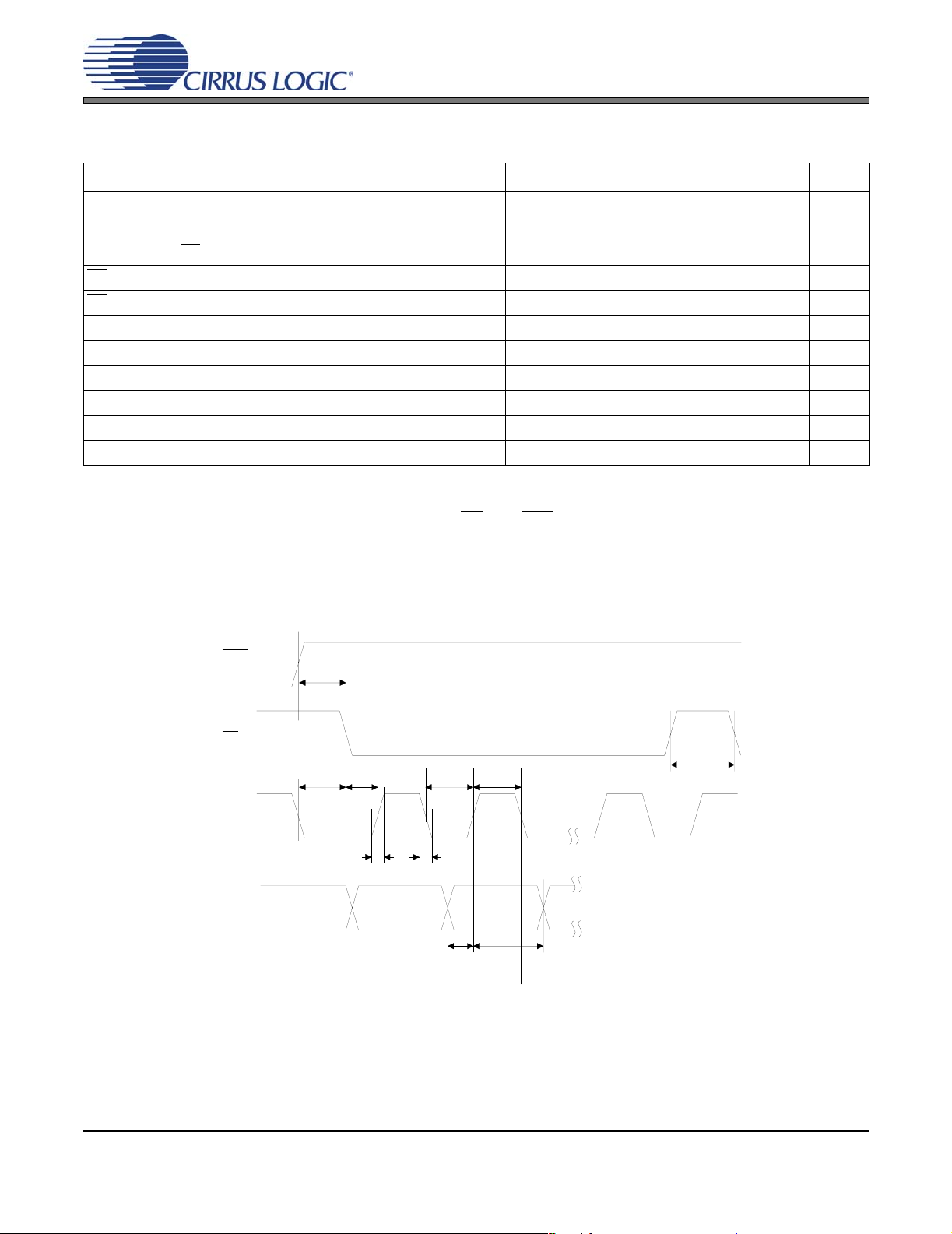
Figure 1. Serial Input Timing..................................................................................................................... 10
Figure 2. Control Port Timing - I²C Format................................................................................................ 11
Figure 3. Control Port Timing - SPI Format (Write)................................................................................... 12
Figure 4. Typical Connection Diagram............................ .... ... ... ... .... ... ... ... ... .... ... ... ... .... ............................ 14
Figure 5. Left-Justified up to 24-Bit Data................................................................................................... 17
Figure 6. I²S, up to 24-Bit Data ................................................................................................................. 17
Figure 7. Right-Justified Data.................................................................................................................... 17
Figure 8. De-Emphasis Curve................................................................................................................... 17
Figure 9. Control Port Timing, I²C Mode................................................................................................... 21
Figure 10.Control Port Timing, SPI mode .................................................................................................. 22
Figure 11.De-Emphasis Curve................................................................................................................... 24
Figure 12.ATAPI Block Diagram ................................................................................................................ 26
Figure 13.Single-Speed (fast) Stopband Rejection.................................................................................... 31
Figure 14.Single-Speed (fast) Transition Band.......................................................................................... 31
Figure 15.Single-Speed (fast) Transition Band (detail).............................................................................. 31
Figure 16.Single-Speed (fast) Passband Ripple........................................................................................ 31
Figure 17.Single-Speed (slow) Stopband Rejection .................................................................................. 31
Figure 18.Single-Speed (slow) Transition Band......................................................................................... 31
Figure 19.Single-Speed (slow) Transition Band (detail)............................................................................. 32
Figure 20.Single-Speed (slow) Passband Ripple....................................................................................... 32
Figure 21.Double-Speed (fast) Stopband Rejection ......................... ......................................... .... ... ... ...... 32
Figure 22.Double-Speed (fast) Transition Band......................................................................................... 32
Figure 23.Double-Speed (fast) Transition Band (detail).......... ... ... .... ... ... ... ... .... ... ... ... ................................ 32
Figure 24.Double-Speed (fast) Passband Ripple....................................................................................... 32
Figure 25.Double-Speed (slow) Stopband Rejection................................................................................. 33
Figure 26.Double-Speed (slow) Transition Band....................................................................................... 33
Figure 27.Double-Speed (slow) Transition Band (detail)........................................................................... 33
Figure 28.Double-Speed (slow) Passband Ripple..................................................................................... 33
DS566F1 3
Page 4

Figure 29.Quad-Speed (fast) Stopband Rejection..................................................................................... 33
Figure 30.Quad-Speed (fast) Transition Band ........................................................................................... 33
Figure 31.Quad-Speed (fast) Transition Band (detail) ............................................................................... 34
Figure 32.Quad-Speed (fast) Passband Ripple ......................................................................................... 34
Figure 33.Quad-Speed (slow) Stopband Rejection........................... ... ... ... ... .... ... ... ... .... ... ... ... ... .... ... ... ... ... 34
Figure 34.Quad-Speed (slow) Transition Band.......................................................................................... 34
Figure 35.Quad-Speed (slow) Transition Band (detail).............................................................................. 34
Figure 36.Quad-Speed (slow) Passband Ripple............................... ... ... ... ... ............................................. 34
LIST OF TABLES
Table 1. CS4351 Auto-Detect.................................................................................................................... 15
Table 2. CS4351 Mode Select................................................................................................................... 15
Table 3. Single-Speed Mode Standard Frequencies.................................................................................16
Table 4. Double-Speed Mode Standard Frequencies................................................................................ 16
Table 5. Quad-Speed Mode Standard Frequencies .................................................................................. 16
Table 6. Digital Interface Format - Stand-Alone Mode............................................................................... 16
Table 7. Digital Interface Formats.............................................................................................................. 24
Table 8. ATAPI Decode ............................................................................................................................. 26
Table 9. Example Digital Volume Settings....... ... .................................................................................... ... 28
Table 10. Revision History......................................................................................................................... 37
CS4351
4 DS566F1
Page 5
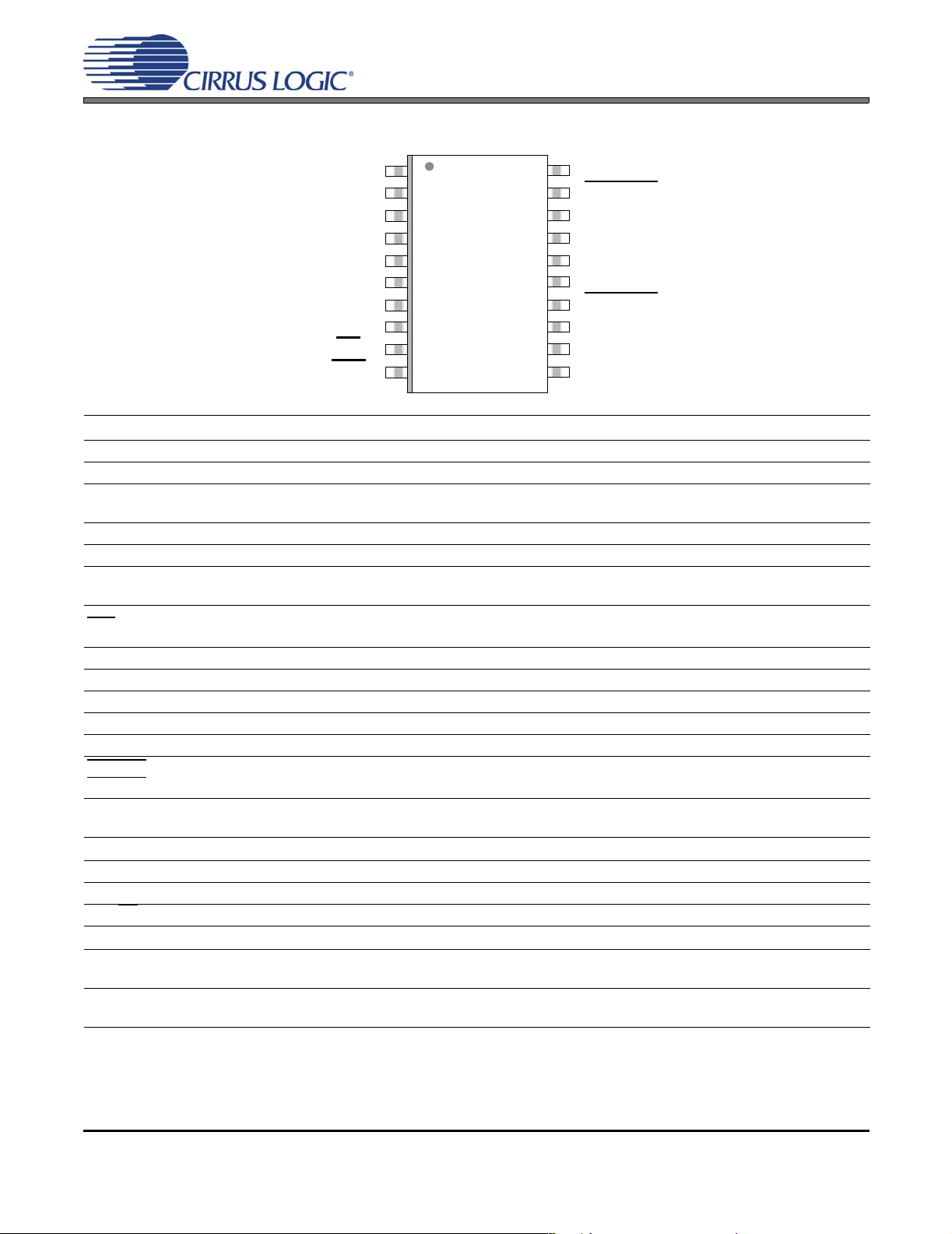
1. PIN DESCRIPTION
CS4351
SDIN VL
SCLK AMUTEC
LRCK AOUTA
MCLK VA_H
VD GND
GND AOUTB
DIF1(SCL/CCLK) BMUTEC
DIF0(SDA/CDIN) VQ
DEM(AD0/CS
) VBIAS
RST
1
2
3
4
5
6
7
8
9
10
20
19
18
17
16
15
14
13
12
11
VA
Pin Name # Pin Description
SDIN 1 Serial Audio Data Input (Input) - Input for two’s complement serial audio data.
SCLK 2 Serial Clock (Input) - Serial clock for the serial audio interface.
LRCK 3
MCLK 4 Master Clock (Input) - Clock source for the delta-sigma modulator and digital filters.
VD 5 Digital Power (Input) - Positive power supply for the digital section.
GND
RST
VA 11 Low Voltage Analog Power (Input) - Positive power supply for the analog section.
VBIAS 12 Positive Voltage Reference (Output) - Positive reference voltage for the internal DAC.
VQ 13 Quiescent Voltage (Output) - Filter connection for internal quiescent voltage.
VA_H 17 High Voltage Analog Power (Input) - Positive power supply for the analog section.
VL 20 Serial Audio Interface Power (Input) - Positive power for the serial audio interface
BMUTEC
AMUTEC
AOUTB
AOUTA
Left / Right Clock (Input) - Determines which channel, Left or Right, is currently active on the serial
audio data line.
6
Ground (Input) - Ground reference.
16
Reset (Input) - Powers down device and resets all internal resisters to their default settings when
10
enabled.
14
Mute Control (Output) - Control signal for optional mute circuit.
19
1518Analog Outputs (Output) - The full scale analog line output level is specified in the Analog Character-
istics table.
Control Port Definitions
SCL/CCLK 7 Serial Control Port Clock (Input) - Serial clock for the control port inter fa ce.
SDA/CDIN 8 Serial Control Data (Input/Output) - Input/Output for I²C data. Input for SPI data.
AD0/CS
9 Address Bit 0 / Chip Select (Input) - Chip address bit in I²C Mode. Control Port enable in SPI Mode.
Stand-Alone Definitions
DIF0
DIF1
DEM 9
87Digital Interface Format (Input) - Defines the required relationship between the Left Right Clock,
Serial Clock, and Serial Audio Data.
De-emphasis (Input) - Selects the standard 15 µs/50 µs digital de-emphasis filter response for 44.1
kHz sample rates
DS566F1 5
Page 6
CS4351
2. CHARACTERISTICS AND SPECIFICATIONS
(Min/Max performance characteristics and specifications are guaranteed over the Specified Operating Conditions.
Typical specifications are derived from performance measurements at T
= 25 °C, VA_H = 12 V, VA = 3.3 V,
A
VD = 3.3 V.)
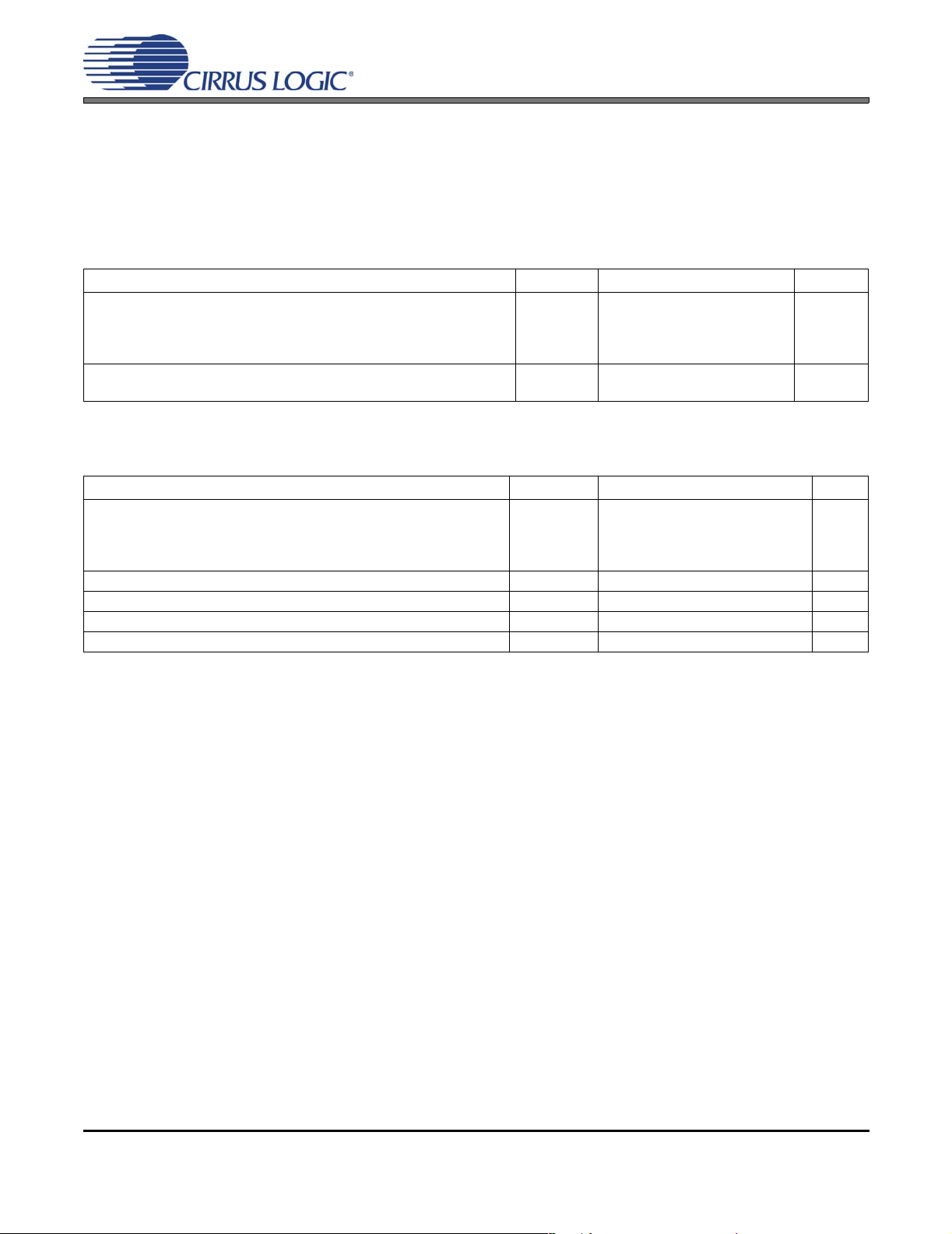
SPECIFIED OPERATING CONDITIONS
(GND = 0 V; all voltages with respect to ground.)
Parameters Symbol Min Typ Max Units
DC Power Supply High Voltage Analog power
Low Voltage Analog power
Digital power
Interface power
Specified Temperature Range -CZZ
-DZZ
V
A_H
V
V
V
T
T
8.55
A
D
L
A
A
3.13
3.13
1.7
-10
-40
12
3.3
3.3
3.3
12.6
3.47
3.47
3.47
-
-
70
85
V
V
V
V
°C
°C
ABSOLUTE MAXIMUM RATINGS
(GND = 0 V; all voltages with respect to ground.)
Parameters Symbol Min Max Units
DC Power Supply High Voltage Analog power
Low Voltage Analog power
Digital power
Interface power
Input Current, Any Pin Except Supplies I
Digital Input Voltage Digital Interface V
Ambient Operating Temperature (power applied) T
Storage Temperature T
Operation at or beyond these limits may result in permanent damage to the device. Normal operation is not guaranteed at these extremes.
V
A_H
V
V
V
in
IN-L
stg
-0.3
A
D
L
A
-0.3
-0.3
-0.3
-±10mA
-0.3 VL+ 0.4 V
-55 125 °C
-65 150 °C
14
3.63
3.63
3.63
V
V
V
V
6 DS566F1
Page 7
CS4351
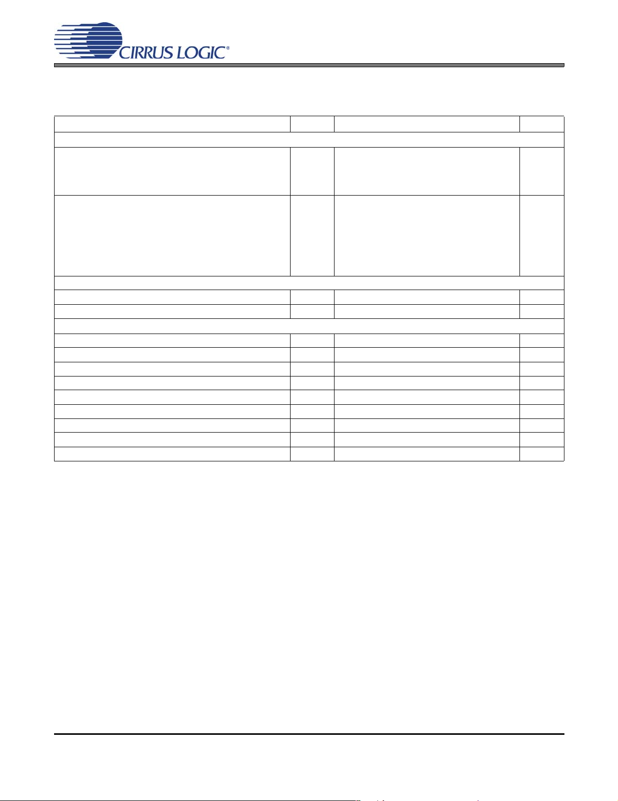
DAC ANALOG CHARACTERISTICS
(Test conditions (unless otherwise specified): input test signal is a 997 Hz sine wave at 0 dBFS; measurement
bandwidth 10 Hz to 20 kHz)
Parameter Symbol Min Typ Max Unit
All Speed Modes Fs = 48, 96, and 192 kHz
Dynamic Range (Note 1) 24-bit unweighted
A-Weighted
16-bit unweighted
A-Weighted
Total Harmonic Distortion + Noise (Note 1)
24-bit 0 dB
-20 dB
-60 dB
16-bit 0 dB
-20 dB
-60 dB
All Speed Modes
Idle Channel Noise / Signal-to-noise ratio - 109 - dB
Interchannel Isolation (1 kHz) - 100 - dB
THD+N -
Analog Output - All Modes
Full Scale Output Voltage 1.85 2.00 2.15 Vrms
Common Mode Voltage V
Max DC Current draw from an AOUT pin I
Max Current draw from VQ I
Interchannel Gain Mismatch - 0.1 - dB
Gain Drift - -10 0 - ppm/°C
Output Impedance Z
AC-Load Resistance R
Load Capacitance C
Q
OUTmax
Qmax
OUT
L
L
99
102
-
-
-
-
-
-
-
-
-4-Vdc
-10-µA
-1-µA
-50-Ω
5--kΩ
--100pF
109
112
95
98
-100
-89
-49
-92
-75
-35
-90
-79
-39
-
-
-
-
-
-
-
dB
dB
dB
dB
dB
dB
dB
dB
dB
dB
Notes:
1. One-half LSB of triangular PDF dither is added to data.
DS566F1 7
Page 8
CS4351
COMBINED INTERPOLATION & ON-CHIP ANALOG FILTER RESPONSE
(The filter characteristics have been normalized to the sample rate (Fs) and can be referenced to the desired sample rate by multiplying the given characteristic by Fs. See
Parameter
Combined Digital and On-Chip Analog Filter Response - Single-Speed Mode - 48 kHz
Passband (Note 3) to -0.01 dB corner
Frequency Response 10 Hz to 20 kHz -0.01 - +0.01 dB
StopBand 0.547 - - Fs
StopBand Attenuation (Note 4) 102 - - dB
Total Group Delay (Fs = Output Sample Rate) - 9.4/Fs - s
Intra-channel Phase Deviation - - ±0.56/Fs s
Inter-channel Phase Deviation - - 0 s
De-emphasis Error (Note 5) Fs = 32 kHz
(Relative to 1 kHz) Fs = 44.1 kHz
Combined Digital and On-Chip Analog Filter Response - Double-Speed Mode - 96 kHz
Passband (Note 3) to -0.01 dB corner
Frequency Response 10 Hz to 20 kHz -0.01 - 0.01 dB
StopBand .583 - - Fs
StopBand Attenuation (Note 4) 80 - - dB
Total Group Delay (Fs = Output Sample Rate) - 4.6/Fs - s
Intra-channel Phase Deviation - - ±0.03/Fs s
Inter-channel Phase Deviation - - 0 s
Combined Digital and On-Chip Analog Filter Response - Quad-Speed Mode - 192 kHz
Passband (Note 3) to -0.01 dB corner
Frequency Response 10 Hz to 20 kHz -0.01 - 0.01 dB
StopBand .635 - - Fs
StopBand Attenuation (Note 4) 90 - - dB
Total Group Delay (Fs = Output Sample Rate) - 4.7/Fs - s
Intra-channel Phase Deviation - - ±0.01/Fs s
Inter-channel Phase Deviation - - 0 s
(Note 6)
to -3 dB corner
Fs = 48 kHz
to -3 dB corner
to -3 dB corner
0
0
-
-
-
0
0
0
0
Fast Roll-Off
-
-
-
-
-
-
-
-
-
.454
.499
±0.23
±0.14
±0.09
.430
.499
.105
.490
UnitMin Typ Max
Fs
Fs
dB
dB
dB
Fs
Fs
Fs
Fs
8 DS566F1
Page 9
CS4351
COMBINED INTERPOLATION & ON-CHIP ANALOG FILTER RESPONSE
(Continued)
Slow Roll-Off (Note 2)
Parameter
Single-Speed Mode - 48 kHz
Passband (Note 3) to -0.01 dB corner
to -3 dB corner
Frequency Response 10 Hz to 20 kHz -0.01 - +0.01 dB
StopBand .583 - - Fs
StopBand Attenuation (Note 4) 64 - - dB
Total Group Delay (Fs = Output Sample Rate) - 6.5/Fs - s
Intra-channel Phase Deviation - - ±0.14/Fs s
Inter-channel Phase Deviation - - 0 s
De-emphasis Error (Note 5) Fs = 32 kHz
(Relative to 1 kHz) Fs = 44.1 kHz
Fs = 48 kHz
0
0
-
-
-
-
-
-
-
-
0.417
0.499
±0.23
±0.14
±0.09
Double-Speed Mode - 96 kHz
Passband (Note 3)) to -0.01 dB corner
to -3 dB corner
Frequency Response 10 Hz to 20 kHz -0.01 - 0.01 dB
StopBand .792 - - Fs
StopBand Attenuation (Note 4) 70 - - dB
Total Group Delay (Fs = Output Sample Rate) - 3.9/Fs - s
Intra-channel Phase Deviation - - ±0.01/Fs s
Inter-channel Phase Deviation - - 0 s
0
0
-
-
.296
.499
Quad-Speed Mode - 192 kHz
Passband (Note 3)) to -0.0 1 dB corner
to -3 dB corner
Frequency Response 10 Hz to 20 kHz -0.01 - 0.01 dB
StopBand .868 - - Fs
StopBand Attenuation (Note 4) 75 - - dB
Group Delay - 4.2/Fs - s
Intra-channel Phase Deviation - ±0.01/Fs s
Inter-channel Phase Deviation - - 0 s
0
0
-
-
.104
.481
UnitMin Typ Max
Fs
Fs
dB
dB
dB
Fs
Fs
Fs
Fs
Notes:
2. Slow Roll-off interpolation filter is only available in Control Port mode.
3. Response is clock dependent and will scale with Fs.
4. For Single-Speed Mode, the Measurement Bandwidth is from stopband to 3 Fs.
For Double-Speed Mode, the Measurement Bandwidth is from stopband to 3 Fs.
For Quad-Speed Mode, the Measurement Bandwidth is from stopband to 1.34 Fs.
5. De-emphasis is available only in Single-Speed Mode; Only 44.1 kHz De-emphasis is available in StandAlone Mode.
6. Amplitude vs. Frequency plots of this data are available in the “Digital Filter Response Plots” on
page 31.
DS566F1 9
Page 10
CS4351
SWITCHING SPECIFICATIONS - SERIAL AUDIO INTERFACE
Parameters Symbol Min Max Units
MCLK Frequency 1.024 51.2 MHz
MCLK Duty Cycle 45 55 %
Input Sample Rate (Manual selection) Single-Speed Mode
Double-Speed Mode
Quad-Speed Mode
Input Sample Rate (Auto selection) Single-Speed Mode
Double-Speed Mode
Quad-Speed Mode
LRCK Duty Cycle 40 60 %
SCLK Pulse Width Low t
SCLK Pulse Width High t
SCLK Period Single-Speed Mode t
Fs
Fs
Fs
Fs
Fs
Fs
sclkl
sclkh
sclkw
4
50
100
4
84
170
50
100
200
50
100
200
20 - ns
20 - ns
1
--------------------- 128()Fs
--
kHz
kHz
kHz
kHz
kHz
kHz
Double-Speed Mode t
Quad-Speed Mode t
SCLK rising to LRCK edge delay t
SCLK rising to LRCK edge setup time t
SDIN valid to SCLK rising setup time t
SCLK rising to SDIN hold time t
LRCK
t
t
slrd
slrs
t
sclkl
SCLK
t
sdlrs
t
sdh
sclkw
sclkw
slrd
slrs
sdlrs
sdh
t
sclkh
1
-----------------64()Fs
2
-----------------
MCLK
--
--
23 - ns
20 - ns
20 - ns
20 - ns
SDATA
Figure 1. Serial Input Timing
10 DS566F1
Page 11
Switching Characteristics - Control Port - I²C® Format
p
(Inputs: Logic 0 = GND, Logic 1 = VL, CL=20pF)
Parameter Symbol Min Max Unit
SCL Clock Frequency f
Rising Edge to Start t
RST
Bus Free Time Between Transmissions t
Start Condition Hold Time (prior to first clock pulse) t
Clock Low time t
Clock High Time t
Setup Time for Repeated Start Condition t
SDA Hold Time from SCL Falling (Note 7) t
SDA Setup time to SCL Rising t
Rise Time of SCL and SDA trc, t
Fall Time SCL and SDA t
Setup Time for Stop Condition t
Acknowledge Delay from SCL Falling t
Notes:
buf
hdst
low
high
sust
hdd
sud
fc
susp
ack
scl
irs
, t
rc
fc
CS4351
- 100 kHz
500 - ns
4.7 - µs
4.0 - µs
4.7 - µs
4.0 - µs
4.7 - µs
0-µs
250 - ns
-1µs
-300ns
4.7 - µs
300 1000 ns
7. Data must be held for sufficient time to bridge the transition time, t
RST
t
irs
Stop Sta rt
SDA
SCL
t
buf
t
hdst
t
low
t
t
high
hdd
t
sud
t
ack
Figure 2. Control Port Timing - I²C Format
, of SCL.
fc
Repeated
Start
t
t
sust
t
hdst
Stop
rd
t
t
rc
t
fd
fc
t
sus
DS566F1 11
Page 12
SWITCHING CHARACTERISTICS - CONTROL PORT - SPI™ FORMAT
(Inputs: Logic 0 = GND, Logic 1 = VL, CL=20pF)
Parameter Symbol Min Max Unit
CCLK Clock Frequency f
RST
Rising Edge to CS Falling t
CCLK Edge to CS
CS High Time Between Transmissions t
CS Falling to CCLK Edge t
CCLK Low Time t
CCLK High Time t
CDIN to CCLK Rising Setup Time t
CCLK Rising to DATA Hold Time (Note 9) t
Rise Time of CCLK and CDIN (Note 10) t
Fall Time of CCLK and CDIN (Note 10) t
Falling (Note 8) t
Notes:
sclk
srs
spi
csh
css
scl
sch
dsu
dh
r2
f2
-6MHz
500 - ns
500 - ns
1.0 - µs
20 - ns
66 - ns
66 - ns
40 - ns
17 - ns
- 100 ns
- 100 ns
CS4351
8. t
only needed before first falling edge of CS after RST rising edge. t
spi
= 0 at all other times.
spi
9. Data must be held for sufficient time to bridge the transition time of CCLK.
10. For F
< 1 MHz.
SCK
RST
t
srs
CS
t
t
spi
css
t
scl
t
sch
CCLK
t
r2
t
f2
CDIN
t
t
dsu
dh
t
csh
Figure 3. Control Port Timing - SPI Format (Write)
12 DS566F1
Page 13

CS4351
DIGITAL CHARACTERISTICS
Parameters Symbol Min Typ Max Units
High-Level Input Voltage VL = 3.3 V
VL = 2.5 V
VL = 1.8 V
Low-Level Input Voltage VL = 3.3 V
VL = 2.5 V
VL = 1.8 V
Input Leakage Current I
Input Capacitance - 8 - pF
Maximum MUTEC Drive Current - 2 - mA
MUTEC High-Level Output Voltage V
MUTEC Low-Level Output Voltage V
V
IH
V
IH
V
IH
V
IL
V
IL
V
IL
in
OH
OL
2.0
1.7
0.65•V
-
-
-
-
-
-
L
-
-
-
-
-
-
0.8
0.7
0.33•V
L
--±10µA
-VA_H- V
-0- V
POWER AND THERMAL CHARACTERISTICS
Parameters Symbol Min Typ Max Units
Power Supplies
Power Supply Current normal operation, V
(Note 11) V
Interface current (Note 12) V
power-down state, all supplies (Note 13)
Power Dissipation (all supplies) (Note 11)
VA_H = 12V normal operation
power-down (Note 13)
VA_H = 9V normal operation
power-down (Note 13)
Power Supply Rejection Ratio (Note 14) (1 kHz)
= 12 V
A_H
= 9 V
A_H
= 3.3 V
V
A
VD= 3.3 V
= 3.3 V
L
(60 Hz)
I
A_H
I
A_H
I
A
I
D
I
L
I
pd
PSRR -
-
-
-
-
-
-
-
-
-
-
-
15
14
6
21
100
200
270
1
216
1
60
60
20
19
8
26
400
-
354
-
285
-
-
-
mW
mW
mW
mW
V
V
V
V
V
V
mA
mA
mA
mA
µA
µA
dB
dB
Notes:
11. Current consumption increases with increasing FS and increasing MCLK. Typ and Max values are
based on highest FS and highest MCLK. Variance between speed modes is small.
12. I
measured with no external loading on pin 8 (SDA).
L
13. Power-Down Mode is defined as RES
14. Valid with the recommended capacitor values on VQ and V
pin = Low with all clock and data lines held static.
as shown in the typical connection dia-
BIAS
gram in Section 3.
DS566F1 13
Page 14
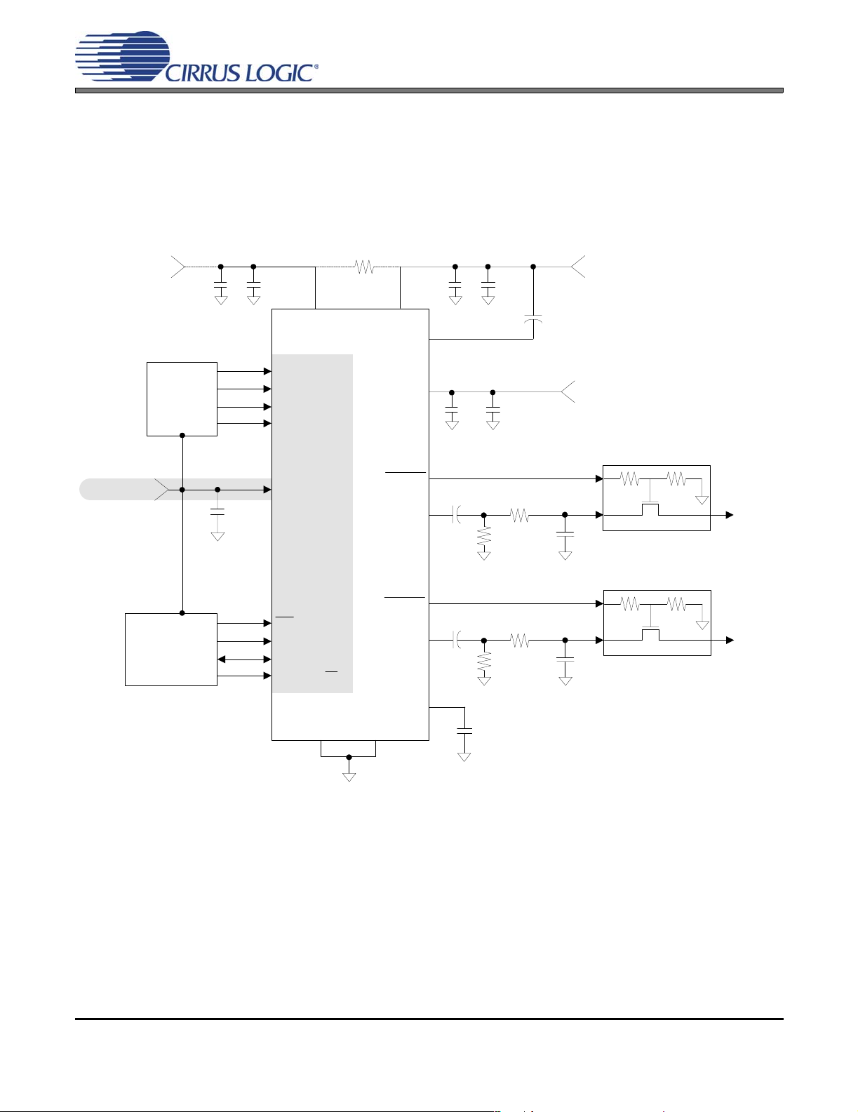
3. TYPICAL CONNECTION DIAGRAM
5.1
+3.3 V *
*Remove this supply if
optional resistor is present.
The decoupling caps should
remain.
10 µF
Digital
Audio
Source
+
0.1 µF
5
VD
4
MCLK
3
LRCK
2
SCLK
1
SDIN
Ω∗
*Optional
11
VA
VBIAS+
VA_H
0.1 µF
12
17
0.1 µF
+
+
10 µF
10 µF
+
CS4351
+3.3 V
3.3 µF
+9 V to +12 V
+1.8 V to VD
µ C/
Mode
Configuration
0.1 µF
20
VL
10
RST
7
DIF1(SCL/CCLK)
8
DIF0(SDA/CDIN)
9
DEM(AD0/CS)
CS4351
GND
6
GND
AMUTEC
AOUTA
BMUTEC
AOUTB
16
VQ
19
18
14
15
13
+
3.3 µF
+
3.3 µF
+
3.3 µF
10 k
10k
560
560
Ω
Ω
Ω
Ω
2.2 nF*
2.2 nF*
*Shown value is
for fc=130kHz
Optional Mute Circuit
576 kΩ412 k
Optional Mute Circuit
576 kΩ412 k
Ω
Ω
AOUTA
AOUTA
Figure 4. Typical Connection Diagram
14 DS566F1
Page 15

4. APPLICATIONS
4.1 Sample Rate Range/Operational Mode Detect
The device operates in one of three operational modes. The allowed sample rate range in each mode will
depend on whether the Auto-Detect Defeat bit is enabled/disabled.
4.1.1 Auto-Detect Enabled
The Auto-Detect feature is enabled by default. In this state, the CS4351 will auto-detect the correct mode
when the input sample rate (F
in Table 1. Sample rates outside the specified range for each mode are not supported.
), defined by the LRCK frequency, falls within one of the ranges illustrated
s
CS4351
Input Sample Rate (F
4 kHz - 50 kHz Single-Speed Mode
84 kHz - 100 kHz Double-Speed Mode
170 kHz - 200 kHz Quad-Speed Mode
4.1.2 Auto-Detect Disabled
The Auto-Detect feature can be defeated only by the format bits in the control port register 02h. In this
state, the CS4351 will not auto-detect the correct mode based on the input sample rate (F
tional mode must then be set manually according to one of the ranges illustrated in Table 2. Please refer
to Section 6.2.3 for implementation details. Sample rates outside the specified range for each mode are
not supported. In stand-alone mode it is not possible to disable auto-detect of sample rates.
FM1 FM0 Input Sample Rate (FS)MODE
0 0 Auto speed mode detect Auto
0 1 4 kHz - 50 kHz Single-Speed Mode
1 0 50 kHz - 100 kHz Double-Speed Mode
1 1 100 kHz - 200 kHz Quad-Speed Mode
4.2 System Clocking
)MODE
S
Table 1. CS4351 Auto-De tect
). The opera-
s
Table 2. CS4351 Mode Select
The device requires external generation of the master (MCLK), left/right (LRCK) and serial (SCLK) clocks.
The left/right clock, defined also as the input sample rate (F
), must be synchronously derived from the
s
MCLK according to specified ratios. The specified ratios of MCLK to LRCK, along with several standard audio sample rates and the required MCLK frequency, are illustrated in Tables 3 through 5.
Refer to Section 4.3 for the required SCLK timing associated with the selected Digital Interface Format and
to the “Switching Specifications - Serial Audio Interface” section on page 10 for the maximum allowed clock
frequencies.
DS566F1 15
Page 16

CS4351
Sample Rate
(kHz)
32 8.1920 12.2880 16.3840 24.5760 32.7680 36.8640
44.1 11.2896 16.9344 22.5792 33.8688 45.1584
48 12.2880 18.4320 24.5760 36.8640 49.1520
256x 384x 512x 768x 1024x 1152x
Table 3. Single-Speed Mode Standard Frequencies
Sample Rate
(kHz)
64 8.1920 12.2880 16.3840 24.5760 32.7680
88.2 11.2896 16.9344 22.5792 33.8688 45.1584
96 12.2880 18.4320 24.5760 36.8640 49.1520
128x 192x 256x 384x 512x
Table 4. Double-Speed Mode Standard Frequencies
Sample Rate
(kHz)
176.4 1 1 .2896 16.9344 22.5792 33.8688 45.1584
192
64x 96x 128x 192x 256x
12.2880 18.4320 24.5760 36.8640 49.1520
Table 5. Quad-Speed Mode Standard Freque n ci es
= Denotes clock modes which are NOT auto detected
MCLK (MHz)
MCLK (MHz)
MCLK (MHz)
4.3 Digital Interface Format
The device will accept audio samples in 1 of 4 digital interface formats in Stand-Alone mode, as illustrated
in Table 6, and 1 of 6 formats in Control Port mode, as illustrated in Table 7.
4.3.1 Stand-Alone Mode
The desired format is selected via the DIF1 and DIF0 pins. For an illustration of the required relationship
between the LRCK, SCLK and SDIN, see Figures 5 through 7. For all formats, SDIN is valid on the rising
edge of SCLK. Also, SCLK must have at least 32 c ycles per LRCK period in format 2, and 48 cycles per
LRCK period in format 3.
DIF0 DIF1 DESCRIPTION FORMAT FIGURE
00
01
10
11
I2S, up to 24-bit Data
Left Justified, up to 24-bit Data
Right Justified, 24-bit Data
Right Justified, 16-bit Data
Table 6. Digital Interface Format - Stand-Alone Mode
4.3.2 Control Port Mode
The desired format is selected via the DIF2, DIF1 and DIF0 bits in the Mode Control 2 register (see section
Section 6.2.1). For an illustration of the required relationship between LRCK, SCLK and SDIN, see
Figures 5 through 7. For all formats, SDIN is v alid on the rising edge of SCLK. Also, SCLK must have at
0 6
1 5
2 7
3 7
16 DS566F1
Page 17

CS4351
least 32 cycles per LRCK period in format 2, 48 cycle s in format 3, 40 cycles in format 4, and 36 cycles
in format 5.
LRCK
SCLK
SDIN +3 +2 +1+5 +4
LRCK
SCLK
SDIN +3 +2 +1+5 +4
LRCK
SCLK
MSB
-1 -2 -3 -4 -5
MSB
-1 -2 -3 -4 -5
Left Channel
Left C hannel
Left Channel
LSB
MSB
-1 -2 -3 -4
Figure 5. Left-Justified up to 24-Bit Data
LSB
MSB
-1 -2 -3 -4
Figure 6. I²S, up to 24-Bit Data
Right Channel
+3 +2 +1+5 +4
Right Channel
+3 +2 +1+5 +4
Right Channel
LSB
LSB
SDIN
MSB
+1 +2 +3 +4
+5
4.4 De-Emphasis Control
The device includes on-chip digital de-emphasis. Figure 8 shows the de-emphasis curve for Fs equal to 44.1
kHz. The frequency response of the de-emphasis curve will scale proportionally with changes in sample
rate, Fs.
-10dB
Gain
dB
0dB
-6 -5 -4 -3 -2 -1-7
LSBMSB
Figure 7. Right-Justified Data
T1=50 µs
T2 = 15 µs
F1 F2
3.183 kHz 10.61 k Hz
Figure 8. De-Emphasis Curve
MSB
+1 +2 +3 +4
Frequency
+5
-6 -5 -4 -3 -2 -1-7
LSB
Note: De-emphasis is only available in Single-Speed Mode.
DS566F1 17
Page 18

4.4.1 Stand-Alone Mode
When pulled to VL the DEM pin activates the 44.1 kHz de-emphasis filter. When pulled to GND the DEM
pin turns off the de-emphasis filter.
4.4.2 Control Port Mode
The Mode Control bits selects either the 32, 44.1, or 48 kHz de-empha sis filter. Plea se see Section 6.2.2
for the desired de-emphasis control.
4.5 Recommended Power-Up Sequence
4.5.1 Stand-Alone Mode
1. Hold RST low until the power supplies and configuration pins are stable, and the master and le ft/right
clocks are locked to the appropriate frequencies, as discussed in Section 4.2. In this state, the control
port is reset to its default settings, VQ will remain low, and VBIAS will be connected to VA.
CS4351
2. Bring RST
Alone power-up sequence after approximately 512 LRCK cycle s in Single-Speed Mode (1024 LRCK
cycles in Double-Speed Mode, and 2048 LRCK cycles in Quad-Speed Mode).
high. The device will remain in a low power state with VQ low and will initiate the Stand-
4.5.2 Control Port Mode
1. Hold RST low until the power supply is stable, and the master and left/right clocks are locked to the
appropriate frequencies, as discussed in Section 4.2. In this state, the control port is reset to its
default settings, VQ will remain low, and VBIAS will be connected to VA.
2. Bring RST
3. Perform a control port write to the CP_EN bit prior to the completion of approximately 512 LRCK
cycles in Single-Speed Mode (1024 LRCK cycles in Double-Speed Mode, and 2048 LRCK cycles in
Quad-Speed Mode). The desired register settings can be loaded wh ile keeping the PDN bit set to 1.
4. Set the PDN bit to 0. This will initiate the power-up sequence, which lasts approximately 50 µs when
the POPG bit is set to 0. If the POPG bit is set to 1, see Section 4.6 for a complete description of
power-up timing.
high. The device will remain in a low power state with VQ low.
4.6 Popguard® Transient Control
The CS4351 uses a novel technique to minimize the effects of output transients du ring power-up and powerdown. This technology, when used with exte rnal DC-blocking capacitors in series with the audio outputs,
minimizes the audio transients commonly produced by single-ended single-s upply converters. It is activated
inside the DAC when the RST
appropriate DC-blocking capacitors.
pin is toggled and requires no other external control, aside from choosing the
4.6.1 Power-Up
When the device is initially powered-up, the audio outputs, AOUTA and AOUTB, are clamped to GND.
Following a delay of approximately 1000 sample periods, each output begins to ramp toward the quiescent voltage. Approximately 10,000 LRCK cycles later, the outputs reach V
This gradual voltage ramping allows time for the external DC-blocking capacitors to charge to the quiescent voltage, minimizing audible power-up transients.
18 DS566F1
and audio output begins.
Q
Page 19

4.6.2 Power-Down
To prevent audible transients at power-down, the device must first enter its power-down state. When this
occurs, audio output ceases and the internal output buffers are disconnected from AOUTA and AOUTB.
In their place, a soft-start current sink is substituted which allows the DC-blocking capacitors to slowly discharge. Once this charge is dissipated, the power to the device may be turn ed off and the system is ready
for the next power-on.
4.6.3 Discharge Time
To prevent an audio transient at the next power-on, the DC-blocking capacitors must fully discharge before turning on the power or exiting the power-down state. If full discharge does not occur, a transient will
occur when the audio outputs are initially clamped to GND. The time that the device must remain in the
power-down state is related to the value of the DC-bl ocking capacitance and the output load. For example,
with a 3.3 µF capacitor, the minimum power-down time will be approximately 0.4 seconds.
4.7 Mute Control
The Mute Control pins go active during power-up initialization, r eset, muting (see Section 6.4.3), or if the
MCLK to LRCK ratio is incorrect. These pins are intended to be used as control for external mute circuits to
prevent the clicks and pops that can occur in any single-ended single supply system.
Use of the Mute Control function is not mandatory but recommended for designs requiring the absolu te minimum in extraneous clicks and pops. Also, use of the Mute Control function can enable the system designer
to achieve idle channel noise/signal-to-noise ratios which are only limited by the external mute circuit.
Please see the “Typical Connection Diagram” on page 14 for a suggested mute circuit for single supply systems. This FET circuit must be placed in series after the RC filter, otherwise noise may occur during muting
conditions. Further ESD protection will need to be taken into consideration for the FET used. If dual supplies
are available, the BJT mute circuit from Figure 12 in the CS4398 datasheet (active Low) may be used.
CS4351
4.8 Grounding and Power Supply Arrangements
As with any high resolution converter, the CS4351 requires careful attention to power supply and grounding
arrangements if its potential performance is to be realized. Figure 4 shows the recommended power arrangements, with VA_H, VA, VD, and VL connected to clean supplies. If the ground planes are split between
digital ground and analog ground, the GND pins of the CS4351 should be connected to the analog ground
plane.
All signals, especially clocks, should be kept away from the VBIAS and VQ pins in order to avoid unwanted
coupling into the DAC.
4.8.1 Capacitor Placement
Decoupling capacitors should be placed as close to the DAC as possible, with the low value ceramic capacitor being the closest. To further minimize impedance, these capacitors should be located on the same
layer as the DAC. If desired, all supply pins may be connected to the same supply, but a decoupling capacitor should still be placed on each supply pin.
Note: All decoupling capacitors should be referenced to analog ground.
The CDB4351 evaluation board demonstrates the optimum layout and power supply arrangements.
DS566F1 19
Page 20

4.9 Control Port Interface
The control port is used to load all the interna l register settings (see Section 6). The operation of the control
port may be completely asynchronous with the audio sample rate. Ho we ver, to a v oid potentia l inter fer ence
problems, the control port pins should remain static if no operation is required.
The control port operates in one of two modes: I²C or SPI.
4.9.1 MAP Auto Increment
The device has MAP (memory address pointer) auto increment capability enabled by the INCR bit (also
the MSB) of the MAP. If INCR is set to 0, MAP will stay constant for successive I²C writes or reads and
SPI writes. If INCR is set to 1, MAP will auto increment after each byte is written, allowing block reads or
writes of successive registers.
4.9.2 I²C Mode
In the I²C mode, data is clocked into and out of the bi-directional serial control data line , SDA, by the serial
control port clock, SCL (see Figure 9 for the clock to data relationship). There is no CS
ables the user to alter the chip address (100110[AD0][R/W
before powering up the device. If the device ever d etects a hi gh to low transition on the AD0/CS
power-up, SPI mode will be selected.
CS4351
pin. Pin AD0 en-
]) and should be tied to VL or GND as required,
pin after
4.9.2.1 I²C Write
To write to the device, follow the procedure below while adhering to the control port Switching Specifications in Section 8.
1. Initiate a START condition to the I²C bus followed by the address byte. The upper 6 bits must be
100110. The seventh bit must match the setting of the AD0 pin, and the eighth must be 0. The eighth
bit of the address byte is the R/W
2. Wait for an acknowledge (ACK) from the part, then write to the memory address pointer, MAP. This
byte points to the register to be written.
3. Wait for an acknowledge (ACK) from the part, then write the desired data to the register p ointed to
by the MAP.
4. If the INCR bit (see Section 4.9.1) is set to 1, repeat the previous step until all the desired registers
are written, then initiate a STOP condition to the bus.
5. If the INCR bit is set to 0 and further I²C writes to other registers are desired, it is necessary to initiate
a repeated START condition and follow the procedure detailed from step 1. If no further writes to other registers are desired, initiate a STOP condition to the bus.
bit.
20 DS566F1
Page 21

CS4351
4.9.2.2 I²C Read
To read from the device, follow the procedure below while adhering to the control port Switching Specifications.
1. Initiate a START condition to the I²C bus followed by the address byte. The upper 6 bits must be
100110. The seventh bit must match the setting of the AD0 pin, and the eighth must be 1. The eighth
bit of the address byte is the R/W
2. After transmitting an acknowledge (ACK), the device will then transmit the contents of the register
pointed to by the MAP. The MAP register will contain the address of the last register written to the
MAP, or the default address (see Section 4.10.2) if an I²C read is the first operation performed on
the device.
3. Once the device has transmitted the contents of the register pointed to by the MAP, issue an ACK.
4. If the INCR bit is set to 1, the device will continue to transmit the contents of successive registers.
Continue providing a clock and issue an ACK after each byte until all the desired registers ar e read,
then initiate a STOP condition to the bus.
5. If the INCR bit is set to 0 and further I²C reads from other registers are desired, it is necessary to
initiate a repeated START condition and follow the procedure detailed from steps 1 and 2 from the
I²C Write instructions followed by step 1 of the I²C Read section. If no further reads from other registers are desired, initiate a STOP condition to the bus.
bit.
4.9.3 SPI Mode
In SPI mode, data is clocked into the serial control data line, CDIN, by the serial control port clock, CCLK
(see Figure 10 for the clock to data relationship). There is no AD0 pin. Pin CS
is used to control SPI writes to the control port. When the device detects a high to low transition on the
AD0/CS
pin after power-up, SPI mode will be selected. All signals are inputs and data is clocked in on the
rising edge of CCLK.
4.9.3.1 SPI Write
To write to the device, follow the procedure below while adhe ring to the control port Switc hing Specifications in Section 8.
NOTE
SDA
SCL
NOTE: If operation is a write, this byte contains the Memory Address Pointer, MAP. If
operation is a read, this byte contains the data of the register pointed to by the MAP.
100110
Start
Figure 9. Control Port Timing, I²C Mode
AD0
R/W
ACK
DATA
1-8
ACK
DATA
1-8
ACK
Stop
is the chip select signal and
1. Bring CS
low.
2. The address byte on the CDIN pin must then be 10011000.
3. Write to the memory address pointer, MAP. This byte points to the register to be written.
DS566F1 21
Page 22

CS4351
4. Write the desired data to the register pointed to by the MAP.
5. If the INCR bit (see Section 4.9.1) is set to 1, repeat the previous step until all the desired registers
are written, then bring CS
6. If the INCR bit is set to 0 and further SPI writes to other registers are desired, it is necessary to bring
CS
high, and follow the procedure detailed from step 1. If no further writes to other register s are de-
sired, bring CS
high.
)
CS
CCLK
high.
CDIN
CHIP
ADDRESS
1001100
MAP = Memory AddressPointer
Figure 10. Control Port Timing, SPI mode
R/W
MAP
MSB
byte 1
DATA
LSB
byte n
4.10 Memory Address Pointer (MAP)
76543210
INCR Reserved Reserved Reserved MAP3 MAP2 MAP1 MAP0
00000000
4.10.1 INC R (AUTO MAP INCREMENT ENABLE)
Default = ‘0’
0 - Disabled
1 - Enabled
4.10.2 MAP (MEMORY ADDRESS POINTER)
Default = ‘0000’
22 DS566F1
Page 23

CS4351
5. REGISTER QUICK REFERENCE
Addr Function 7 6 5 4 3 2 1 0
1h Chip ID PART4 PART3 PART2 PART1 PART0 REV2 REV1 REV0
default 1 1 1 1 1 - - -
2h Mode Control Reserved DIF2 DIF1 DIF0 DEM1 DEM0 FM1 FM0
default0000 0000
3h Volume, Mixing,
and Inversion
Control
default0000 1001
4h Mute Control AMUTE Reserved MUTEC
default1000 0000
5h Channel A Volume
Control
default0000 0000
6h Channel B Volume
Control
default0000 0000
7h Ramp and Filter
Control
default1011 0001
8h Misc. Control PDN CPEN FREEZ E Reserved Reserved Reserved Reserved Reserved
default1000 0000
VOLB=A INVERTA INVERTB Reserved ATAPI3 ATAPI2 ATAPI1 ATAPI0
MUTE_A MUTE_B Reserved Reserved Reserved
A=B
VOL7 VOL6 VOL5 VOL4 VOL3 VOL2 VOL1 VOL0
VOL7 VOL6 VOL5 VOL4 VOL3 VOL2 VOL1 VOL0
SZC1 SZC0 RMP_UP RMP_DN Reserved FILT_SEL Reserved Reserved
DS566F1 23
Page 24

CS4351
6. REGISTER DESCRIPTION
** All register access is R/W unless specified otherwise**
6.1 Chip ID - Register 01h
76543210
PART4 PART3 PART2 PART1 PART0 REV2 REV1 REV0
11111- - -
Function:
This register is Read-Only. Bits 7 through 3 are the part number ID which is 111 11b a nd th e remainin g Bits
(2 through 0) are for the chip revision (Rev. A = 000, Rev. B = 001, ...)
6.2 Mode Control 1 - Register 02h
76543210
Reserved DIF2 DIF1 DIF0 DEM1 DEM0 FM1 FM0
00000000
6.2.1 Digital Interface Format (DIF2:0) Bits 6-4
Function:
These bits select the interface format for the serial audio input.
The required relationship between the Left/Right clock, serial clock and serial data is defined by the Digital
Interface Format and the options are detailed in Figures 5 through 7.
DIF2 DIF1 DIF0 DESCRIPTION Format FIGURE
000
001
010
011
100
101
110
111
Left Justified, up to 24-bit data 0 (Default)
I2S, up to 24-bit data
Right Justified, 16-bit data
Right Justified, 24-bit data
Right Justified, 20-bit data
Right Justified, 18-bit data
Reserved
Reserved
Table 7. Digital Interface Formats
6.2.2 De-Emphasis Control (DEM1:0) Bits 3-2.
Default = 0
00 - No De-emphasis
01 - 44.1 kHz De-emphasis
10 - 48 kHz De-emphasis
11 - 32 kHz De-emphasis
Function:
5
1 6
2 7
3 7
4 7
5 7
Gain
dB
T1=50 µs
0dB
T2 = 15 µs
-10dB
Selects the appropriate digital filter to maintain th e standard 15 µs/50 µs digital de-emphasis filter response at
F1 F2
3.183 kHz 10.61 kHz
Frequency
32, 44.1 or 48 kHz sample rates. (See Figure 11.)
Figure 11. De-Emphasis Curve
Note: De-emphasis is only available in Single-Speed Mode
24 DS566F1
Page 25

CS4351
6.2.3 Functional Mode (FM) Bits 1-0
Default = 00
00 - Auto speed mode detect
01 - Single-Speed Mode (4 to 50 kHz sample rates)
10 - Double-Speed Mode (50 to 100 kHz sample rates)
11 - Quad-Speed Mode (100 to 200 kHz sample rates)
Function:
Selects the required range of input sample rates or DSD Mode.
6.3 Volume Mixing and Inversion Control - Register 03h
B7 B6 B5 B4 B3 B2 B1 B0
VOLB=A INVERT A INVERT B Reserved ATAPI3 ATAPI2 ATAPI1 ATAPI0
00001001
6.3.1 Channel A Volume = Channel B Volume (VOLB=A) Bit 7
Function:
When set to 0 (default) the AOUTA and AOUTB volume levels are independently controlled by the A and
the B Channel Volume Control Bytes.
When set to 1 the volume on both AOUTA and AOUTB are determined by the A Ch annel Attenuation and
Volume Control Bytes, and the B Channel Bytes are ignored.
6.3.2 Invert Signal Polarity (Invert_A) Bit 6
Function:
When set to 1, this bit inverts the signal polarity of channel A.
When set to 0 (default), this function is disabled.
6.3.3 Invert Signal Polarity (Invert_B) Bit 5
Function:
When set to 1, this bit inverts the signal polarity of channel B.
When set to 0 (default), this function is disabled.
DS566F1 25
Page 26

6.3.4 ATAPI Channel Mixing and Muting (ATAPI3:0) Bits 3-0
Default = 1001 - AOUTA=aL, AOUTB=bR (Stereo)
Function:
The CS4351 implements the channel mixing functions of the ATAPI CD-ROM specification. Refer to
Table 8 and Figure 12 for additional information.
CS4351
Left Channel
Audio Data
A Channel
Volume
Control
ΣΣ
Right Channel
Audio Data
Figure 12. ATAPI Block Diagram
ATAPI3 ATAPI2 ATAPI1 ATAPI0 AOUTA AOUTB
0 0 0 0 MUTE MUTE
0001 MUTE bR
0010 MUTE bL
0 0 1 1 MUTE b[(L+R)/2]
0100 aR MUTE
0101 aR bR
0110 aR bL
0 1 1 1 aR b[(L+R)/2]
1000 aL MUTE
1001 aL bR
1010 aL bL
1 0 1 1 aL b[(L+R)/2]
1 1 0 0 a[(L+R)/2] MUTE
1 1 0 1 a[(L+R)/2] bR
1 1 1 0 a[(L+R)/2] bL
1 1 1 1 a[(L+R)/2] b[(L+R)/2]
T able 8. ATAPI Decode
B Channel
Volume
Control
MUTE
MUTE
AoutA
AoutB
26 DS566F1
Page 27

CS4351
6.4 Mute Control - Register 04h
76543210
AMUTE Reserved MUTEC A=B MUTE_A MUTE_B Reserved Reserved Reserved
10000000
6.4.1 Auto-Mute (AMUTE) Bit 7
Function:
When set to 1 (default), the Digital-to-Analog converter output will mute following the reception of 8192
consecutive audio samples of static 0 or -1. A single sample of non-static data will release the mute. Detection and muting is done independently for each channel. The quiescent voltage on the output will be
retained and the Mute Control pin will go active during the mute period. When set to 0, this function is
disabled
6.4.2 AMUTEC = BMUTEC (MUTEC A=B) Bit 5
Function:
When set to 0 (default), the AMUTEC and BMUTEC pins operate independently.
When set to 1, the individual controls for AMUTEC and BMUTEC are internally connected through an
AND gate prior to the output pins. Therefore, the external AMUTEC and BMUTEC pins will go active only
when the requirements for both AMUTEC and BMUTEC are valid.
6.4.3 A Channel Mute (MUTE_A) Bit 4 B Channel Mute (MUTE_B) Bit 3
Function:
When set to 1, the Digital-to-Analog converter output will mute. The quiescent voltage on the output will
be retained. The muting function is effected, similar to attenuation changes, by the Soft and Zero Cross
bits in the Volume and Mixing Control register. The corresponding MUTEC pin will go active following any
ramping due to the soft and zero cross function.
When set to 0 (default), this function is disabled.
6.5 Channel A Volume Control - Register 05h
Channel B Volume Control - Register 06h
76543210
VOL7 VOL6 VOL5 VOL4 VOL3 VOL2 VOL1 VOL0
00000000
DS566F1 27
Page 28

CS4351
6.5.1 Digital Volume Control (VOL7:0) Bits 7-0
Default = 00h (0 dB)
Function:
The Digital Volume Control registers allow independent control of the signal levels in 1/2 dB increments
from 0 to -127.5 dB. Volume settings are decoded as shown in Table 9. The volume changes are implemented as dictated by the Soft and Zero Cross bits in the Power and Muting Control register.
The actual attenuation is determ ined by taking the decimal value of the volume register and multiplying
by 6.02/12.
Binary Code Decimal Value Volume Setting
00000000 0 0 dB
00000001 1 -0.5 dB
00000110 6 -3.0 dB
11111111 255 -127.5 dB
Table 9. Example Digital Volume Settings
6.6 Ramp and Filter Control - Register 07h
76543210
SZC1 SZC0 RMP_UP RMP_DN Reserved FILT_SEL Reserved Reserved
10110001
6.6.1 Soft Ramp and Zero Cross Control (SZC1:0) Bits 7-6
Default = 10
SZC1 SZC0 Description
0 0 Immediate Change
01 Zero Cross
10 Soft Ramp
1 1 Soft Ramp on Zero Crossings
Function:
Immediate Change
When Immediate Change is selected all level changes will take effect immediately in one step.
Zero Cross
Zero Cross Enable dictates that signal level changes, either by attenuation changes or muting, will occur
on a signal zero crossing to minimize audible artifacts. The requested level change will occur after a timeout period between 512 and 1024 sample periods (10.7 ms to 21.3 ms at 48 kHz sample rate) if the signal
does not encounter a zero crossing. The zero cross function is independently monitored and impl emented
for each channel.
Soft Ramp PCM
Soft Ramp allows level changes, both muting and attenuation, to be implemented by incrementally ramp-
ing, in 1/8 dB steps, from the current level to the new level at a rate of 1 dB per 8 left/right clock periods.
28 DS566F1
Page 29

Soft Ramp and Zero Cross
Soft Ramp and Zero Cross Enable dictate that signal leve l changes, either by attenuation changes or mut-
ing, will occur in 1/8 dB steps and be implemented on a signal zero crossing. The 1/8 dB level change will
occur after a time-out period between 512 and 10 24 sample periods (10.7 ms to 21.3 ms at 48 kHz sample
rate) if the signal does not encounter a zer o crossing. The zer o cross function is inde pendently monito red
and implemented for each channel.
6.6.2 Soft Volume Ramp-Up After Error (RMP_UP) Bit 5
Function:
When set to 1 (default), an un-mute will be performed after executing a filter mode change, after a
LRCK/MCLK ratio change or error, and after cha nging the Functional Mode. This un-mute is affected, similar to attenuation changes, by the Soft and Zero Cross bits in the Volume and Mixing Control register.
When set to 0, an immediate un-mute is performed in these instances.
Note: For best results, it is recommended this feature be used in conjunction with the RMP_DN bit.
6.6.3 Soft Ramp-Down Before Filter Mode Change (RMP_DN) Bit 4
Function:
When set to 1 (default), a mute will be performed prior to executing a filter mode change. This mute is
affected, similar to attenuation changes, by the Soft and Zero Cr oss bits in the Volume and Mixing Control
register.
CS4351
When set to 0, an immediate mute is performed prior to executing a filter mode change.
Note: For best results, it is recommended that this feature be used in conjunction with the RMP_UP bit.
6.6.4 Interpolation Filter Select (FILT_SEL) Bit 2
Function:
When set to 0 (default), the Interpolation Filter has a fast roll off.
When set to 1, the Interpolation Filter has a slow roll off.
The specifications for each filter can be found in the “Co mbined Interpolation & On-Chip Analog Filter Re-
sponse” section on page 8, and response plots can be found in Figures 15 to 36.
6.7 Misc Control - Register 08h
76543210
PDN CPEN FREEZE Reserved Reserved R eserved Reserved Reserved
10000000
DS566F1 29
Page 30

6.7.1 Power Down (PDN) Bit 7
Function:
When set to 1 (default), the entire device will enter a low-power state and the contents of the control reg-
isters will be retained. The power-down bit defaults to ‘1’ on power-up and must be disabled before normal
operation in Control Port mode can occur. This bit is ignored if CPEN is not set.
6.7.2 Control Port Enable (CPEN) Bit 6
Function:
This bit is set to 0 by default, allowing the device to power-up in Stand-Alone Mode. Control Port Mode
can be accessed by setting this bit to 1. This will allow operation of the device to be controlled by the registers and the pin definitions will conform to Control Port Mode.
6.7.3 Freeze Controls (Freeze) Bit 5
Function:
When set to 1, this function allows modifications to be made to the registers without the changes taking
effect until FREEZE is set back to 0. To make multiple changes in the Control Port registers take effect
simultaneously, enable the FREEZE bit, make all register changes, then disable the FREEZE bit.
CS4351
When set to 0 (default), register changes take effect immediately.
30 DS566F1
Page 31

7. DIGITAL FILTER RESPONSE PLOTS
1
6
5
5
1
6
CS4351
0
−20
−40
−60
Amplitude (dB)
−80
−100
−120
0.4 0.5 0.6 0.7 0.8 0.9
Frequency(normalized to Fs)
0
−20
−40
−60
Amplitude (dB)
−80
−100
−120
0.4 0.42 0.44 0.46 0.48 0.5 0.52 0.54 0.56 0.58 0.
Frequency(normalized to Fs)
Figure 13. Single-Speed (fast) Stopband Rejection Figure 14. Single-Speed (fast) Transition Band
0
−1
−2
−3
−4
−5
Amplitude (dB)
−6
−7
−8
−9
−10
0.45 0.46 0.47 0.48 0.49 0.5 0.51 0.52 0.53 0.54 0.5
Frequency(normalized to Fs)
0.02
0.015
0.01
0.005
0
Amplitude (dB)
−0.005
−0.01
−0.015
−0.02
0 0.05 0.1 0.15 0.2 0.25 0.3 0.35 0.4 0.45 0.
Frequency(normalized to Fs)
Figure 15. Single-Speed (fast) Transition Band (detail) Figure 16. Single-Speed (fast) Passband Ripple
0
−20
−40
−60
Amplitude (dB)
−80
−100
−120
0.4 0.5 0.6 0.7 0.8 0.9
Frequency(normalized to Fs)
0
−20
−40
−60
Amplitude (dB)
−80
−100
−120
0.4 0.42 0.44 0.46 0.48 0.5 0.52 0.54 0.56 0.58 0.
Frequency(normalized to Fs)
Figure 17. Single-Speed (slow) Stopband Rejection Figure 18. Single-Speed (slow) Transition Band
DS566F1 31
Page 32

CS4351
5
5
1
6
5
5
0
−1
−2
−3
−4
−5
Amplitude (dB)
−6
−7
−8
−9
−10
0.45 0.46 0.47 0.48 0.49 0.5 0.51 0.52 0.53 0.54 0.5
Frequency(normalized to Fs)
Figure 19. Single-Speed (slow) Transition Band (detail) Figure 20. Single-Speed (slow) Passband Ripple
0.02
0.015
0.01
0.005
0
Amplitude (dB)
−0.005
−0.01
−0.015
−0.02
0 0.05 0.1 0.15 0.2 0.25 0.3 0.35 0.4 0.45 0.
Frequency(normalized to Fs)
0
20
40
60
Amplitude (dB)
80
100
120
0.4 0.5 0.6 0.7 0.8 0.9
Frequency(normalized to Fs)
0
20
40
60
Amplitude (dB)
80
100
120
0.4 0.42 0.44 0.46 0.48 0.5 0.52 0.54 0.56 0.58 0.
Frequency(normalized to Fs)
Figure 21. Double-Speed (fast) Stopband Rejection Figure 22. Double-Speed (fast) Transition Band
0
1
2
3
4
5
Amplitude (dB)
6
7
8
9
10
0.45 0.46 0.47 0.48 0.49 0.5 0.51 0.52 0.53 0.54 0.5
Frequency(normalized to Fs)
0.02
0.015
0.01
0.005
0
Amplitude (dB)
0.005
0.01
0.015
0.02
0 0.05 0.1 0.15 0.2 0.25 0.3 0.35 0.4 0.45 0.
Frequency(normalized to Fs)
Figure 23. Double-Speed (fast) Transition Band (detail) Figure 24. Double-Speed (fast) Passband Ripple
32 DS566F1
Page 33

1
8
5
5
1
8
CS4351
0
20
40
60
Amplitude (dB)
80
100
120
0.2 0.3 0.4 0.5 0.6 0.7 0.8 0.9
Frequency(normalized to Fs)
0
20
40
60
Amplitude (dB)
80
100
120
0.2 0.3 0.4 0.5 0.6 0.7 0.
Frequency(normalized to Fs)
Figure 25. Double-Speed (slow) Stopband Rejection Figure 26. Double-Speed (slow) Transition Band
0
1
2
3
4
5
Amplitude (dB)
6
7
8
9
10
0.45 0.46 0.47 0.48 0.49 0.5 0.51 0.52 0.53 0.54 0.5
Frequency(normalized to Fs)
0.02
0.015
0.01
0.005
0
Amplitude (dB)
0.005
0.01
0.015
0.02
0 0.05 0.1 0.15 0.2 0.25 0.3 0.3
Frequency(normalized to Fs)
Figure 27. Double-Speed (slow) Transition Band (detail) Figure 28. Double-Speed (slow) Passband Ripple
0
20
40
60
Amplitude (dB)
80
100
120
0.2 0.3 0.4 0.5 0.6 0.7 0.8 0.9
Frequency(normalized to Fs)
0
20
40
60
Amplitude (dB)
80
100
120
0.2 0.3 0.4 0.5 0.6 0.7 0.
Frequency(normalized to Fs)
Figure 29. Quad-Speed (fast) Stopband Rejection Figure 30. Quad-Speed (fast) Transition Band
DS566F1 33
Page 34

5
5
1
9
5
2
CS4351
0
1
2
3
4
5
Amplitude (dB)
6
7
8
9
10
0.45 0.46 0.47 0.48 0.49 0.5 0.51 0.52 0.53 0.54 0.5
Frequency(normalized to Fs)
0.2
0.15
0.1
0.05
0
Amplitude (dB)
0.05
0.1
0.15
0.2
0 0.05 0.1 0.15 0.2 0.2
Frequency(normalized to Fs)
Figure 31. Quad-Speed (fast) Transition Band (detail) Figure 32. Quad-Speed (fast) Passband Ripple
0
20
40
60
Amplitude (dB)
80
0
20
40
60
Amplitude (dB)
80
100
120
0.1 0.2 0.3 0.4 0.5 0.6 0.7 0.8 0.9
Frequency(normalized to Fs)
100
120
0.1 0.2 0.3 0.4 0.5 0.6 0.7 0.8 0.
Frequency(normalized to Fs)
Figure 33. Quad-Speed (slow) Stopband Rejection Figure 34. Quad-Speed (slow) Transition Band
0
1
2
3
4
5
Amplitude (dB)
6
7
8
9
10
0.45 0.46 0.47 0.48 0.49 0.5 0.51 0.52 0.53 0.54 0.5
Frequency(normalized to Fs)
0.02
0.015
0.01
0.005
0
Amplitude (dB)
0.005
0.01
0.015
0.02
0 0.02 0.04 0.06 0.08 0.1 0.1
Frequency(normalized to Fs)
Figure 35. Quad-Speed (slow) Transition Band (detail) Figure 36. Quad-Speed (slow) Passband Ripple
34 DS566F1
Page 35

8. PARAMETER DEFINITIONS
Total Harmonic Distortion + Noise (THD+N)
The ratio of the rms value of the signal to the rms sum of all other spectral components over the specified
bandwidth (typically 10 Hz to 20 kHz), including distortion components. Expressed in decibels.
Dynamic Range
The ratio of the full scale rms value of the signal to the rms sum of all other spectral components over the
specified bandwidth. Dynamic range is a signal-to-noise measurement over the specified bandwidth made
with a -60 dBFS signal. 60 dB is then added to the resulting measurement to refer the measurement to full
scale. This technique ensures that the distortion components are below the noise le vel and do not effect the
measurement. This measurement technique has bee n accepted by the Audio En gineering Society, AES171991, and the Electronic Industries Association of Japan, EIAJ CP-307.
Interchannel Isolation
A measure of crosstalk between the left and right channels. Measured for each channel at the conver ter's
output with all zeros to the input under test and a full- scale signal applied to the other channel. Units in decibels.
Interchannel Gain Mismatch
The gain difference between left and right channels. Units in decibels.
CS4351
Gain Error
The deviation from the nominal full scale analog output for a full scale digital input.
Gain Drift
The change in gain value with temperature. Units in ppm/°C.
Intra-Channel Phase Deviation
The deviation from linear phase within a given channel.
Inter-Channel Phase Deviation
The difference in phase between channels.
DS566F1 35
Page 36

9. PACKAGE DIMENSIONS 20L TSSOP (4.4 mm BODY) PACKAGE DRAWING
N
CS4351
1
23
TOP VIEW
D
E
e
2
b
SIDE VIEW
A2
A1
A
SEATING
PLANE
L
INCHES MILLIMETERS
1
E1
END VIEW
NOTE
DIM MIN NOM MAX MIN NOM MAX
A -- -- 0.043 -- -- 1.10
A1 0.002 0.004 0.006 0.05 -- 0.15
A2 0.03346 0.0354 0.037 0.85 0.90 0.95
b 0.00748 0.0096 0.012 0.19 0.245 0.30 2,3
D 0.252 0.256 0.259 6.40 6.50 6.60 1
E 0.248 0.2519 0.256 6.30 6.40 6.50
E1 0.169 0.1732 0.177 4.30 4.40 4.50 1
e -- -- 0.026 -- -- 0.65
L 0.020 0.024 0.028 0.50 0.60 0.70
µ
0° 4° 8° 0° 4° 8°
∝
JEDEC #: MO-153
Controlling Dimension is Millimeters.
Notes:
1. “D” and “E1” are reference datums and do not included mold flash or protrusions, but do include mold mismatch and are measured at the parting line, mold flash or protrusions shall not exceed 0.20 mm per side.
2. Dimension “b” does not include dambar protrusion/intrusion. Allowable dambar protrusion shal l be 0.13 mm
total in excess of “b” dimension at maximum material condition. Dambar intrusion shall not reduce dimension “b” by more than 0.07 mm at least material condition.
3. These dimensions apply to the flat section of the lead between 0.10 and 0.2 5 mm from lead tips.
Parameters Symbol Min Typ Max Units
Package Thermal Resistance 20L TSSOP θ
JA
-72-°C/Watt
36 DS566F1
Page 37

CS4351
10.ORDERING INFORMATION
Product Description Package Pb-Free Grade Temp Range Container Order #
CS4351
CDB4351 CS4351 Evaluation Board - - - -
192 kHz Stereo DAC
with 2 Vrms Line Out
20-pin
TSSOP
YES
Commercial -10° to +70° C
Automotive -40 ° to +85° C
Rail
Tape & Reel
Rail
Tape & Reel
CS4351-CZZ
CS4351-CZZR
CS4351-DZZ
CS4351-DZZR
CDB4351
11.REVISION HISTORY
Release Date Changes
PP3 March 2005 Removed CS4351-CZ ordering option.
Added CS4351-DZZ ordering option.
Updated Tslrd spec on page 10.
Updated Tdh spec on page 12.
Updated VIL specification on page 13.
Updated legal text.
PP4 July 2005 Updated full-scale output specification on page 7.
Updated gain drift on page 7
Updated ordering information.
F1 December 2005 Updated status to final
Updated legal text
Table 10. Revision History
Contacting Cirrus Logic Support
For all product questions and inquiries, contact a Cirrus Logic Sales Representative.
To find one nearest you, go to www.cirrus.com/corporate/contacts/sales.cfm
IMPORTANT NOTICE
Cirrus Logic, Inc. an d i ts su bsi di a ri e s ("Ci r r us ") be li eve th at the information con tai n ed in t his doc ument i s ac cu ra te an d r eliable. However, the in f ormat i o n i s s ubj ec t
to change without noti ce and is pr ovided "AS I S" without war ranty of a ny kind (expr ess or impl ied). Custo mers are adv ised to ob tain the latest version of relevant
information to verify, before placing orders, that information being relied on is current and complete. All products are sold subject to the terms and conditions of sale
supplied at the time of order acknowledgment, including those pertaining to warranty, indemnification, and limitation of liability. No responsibility is assumed by Cirrus
for the use of this information, including use of this information as the basis for manufacture or sale of any items, or for infringement of patents or other rights of third
parties. This document is the property of Cirrus and by furnishing this information, Cirrus grants no license, express or implied under any patents, mask work rights,
copyrights, trademarks, trade secrets or other intellectual pr operty rights. Cirrus owns the copyrigh ts associated w ith the information contained herein and gives consent for copies to be made of the information only for u s e within your organization with respect to Cirrus integrated circuits or other products of Cirrus. This consent
does not extend to other copying such as copying for general distribution, advertising or promotional purposes, or for creating any work for resale.
CERTAIN APPLICATIONS USING SEMICONDUCTOR PRODUCTS MAY INVOLVE POTENTIAL RISKS OF DEATH, PERSONAL INJURY, OR SEVERE PROPERTY OR ENVIRONMENTAL DAMAGE (“CRITICAL APPLICATIONS”). CIRRUS PRODUCTS ARE NOT DESIGNED, AUTHORIZED OR WARRANTED FOR USE
IN AIRCRAFT SYSTEMS, MILITARY APPLICATIONS, PRODUCTS SURGICALLY IMPLANTED INTO THE BODY, AUTOMOTIVE SAFETY OR SECURITY DEVICES, LIFE SUPPORT PRODUCTS OR OTHER CRITICAL APPLICATIONS. INCLUSION OF CIRRUS PRODUCTS IN SUCH APPLICATIONS IS UNDERSTOOD
TO BE FULLY AT THE CUSTOMER’S RISK AND CIRRUS DISCLAIMS AND MAKES NO WARRANTY, EXPRESS, STATUTORY OR IMPLIED, INCLUDING THE
IMPLIED WARRANTIES OF MERCHANTABILITY AND FI TNESS FOR PARTICULA R PURPOSE, WITH REGARD TO ANY CI RRUS PR ODUCT T HAT I S USED
IN SUCH A MANNER. IF THE CUSTOMER OR CUSTOMER’S CUSTOMER USES OR PERMITS THE USE OF CIRRUS PRODUCTS IN CRITICAL APPLICATIONS, CUSTOMER AGREES, BY SUCH USE, TO FULLY INDEMNIFY CIRRUS, ITS OFFICERS, DIRECTORS, EMPLOYEES, DISTRIBUTORS AND OTHER
AGENTS FROM ANY AND ALL LIABILITY, INCLUDING ATTORNEYS’ FEES AND COSTS, THAT MAY RESULT FROM OR ARISE IN CONNECTION WITH THESE
USES.
Cirrus Logic, Cirrus , t h e Ci rr us L ogi c l og o des i gn s, and Po pg ua rd ar e t r ad emar ks of Ci rr us L og ic , Inc . Al l ot h er br and an d p roduct names in this document may be
trademarks or service marks of their respective owners.
SPI is a trademark of Motorola, Inc.
I²C is a registered trademark of Philips Semiconductor.
DS566F1 37
 Loading...