

Page 1
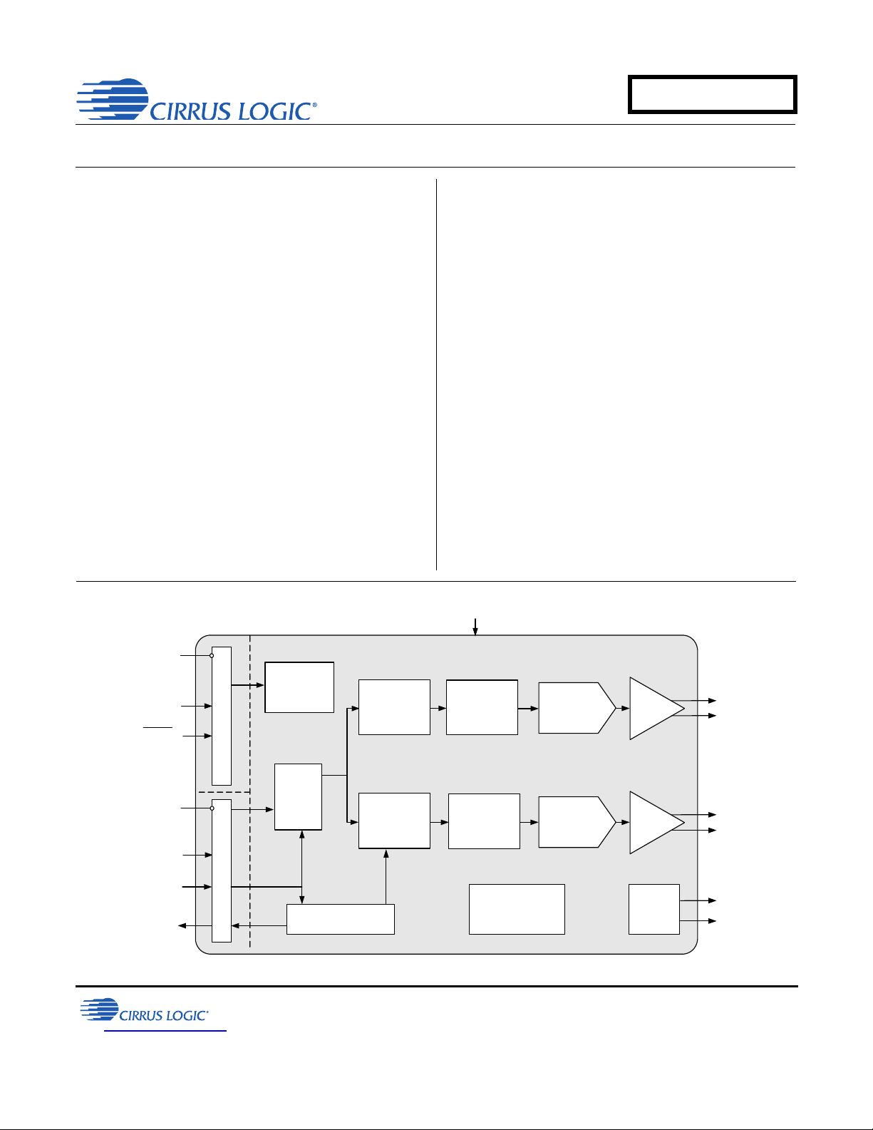
192-kHz Stereo DAC with Integrated PLL
PCM
Serial
Interface
Serial Audio Input
Right
Channel
Output
Left
Channel
Output
Reset
3.3 V to 5.0 V
Register/
Hardware
Configuration
Hardware or I2C/
SPI Control Data
3.3 V to 5.0 V
LRCK
RMCK
RMCK
Recovered MCLK
1.5 V to 5.0 V
Internal Voltage
Reference
and Regulation
Phase Locked Loop
Interpolation
Filter with
Volume
Control
Interpolation
Filter with
Volume
Control
Multibit
Modulator
Multibit
Modulator
Level Translator Level Translator
Amp
+
Filter
Amp
+
Filter
Left and
Right Mute
Controls
External
Mute
Control
DAC
DAC
Features
Advanced multibit delta-sigma architecture
109 dB dynamic range
-91 dB THD+N
24-bit conversion
Supports audio sample rates up to 192 kHz
Low-latency digital filtering
Single-ended or differential analog output
architecture
Integrated PLL locks to incoming left-right
clock
– Eliminates the need for external master-
clock routing
– Reduces interference and jitter sensitivity
– No external loop filter components required
Automatic sample-rate range detection
CS4350
Popguard
pops
Hardware popguard disable for fast startups
Supports all standard serial audio formats
including time-division multiplexed (TDM)
+1.5- to 5.0-V logic supplies for serial port
+3.3- to 5.0-V control port interface
Control Port Mode Features
SPI™ and I²C
ATAPI mixing
Mute control for individual channels
Digital volume control with soft ramp
– 127.5 dB attenuation
– 1/2 dB step size
– Zero-crossing click-free transitions
®
technology for control of clicks and
™
Modes
http://www.cirrus.com
Copyright Cirrus Logic, Inc. 2013
(All Rights Reserved)
APR ‘13
DS691F2
Page 2

CS4350
Description
The CS4350 is a complete stereo digital-to-analog system including PLL-based master clock derivation, digital interpolation, 5th-order multibit delta-sigma digital-to-analog conversion, digital de-emphasis, volume control, channel
mixing, and analog filtering. The advantages of this architecture include ideal differential linearity, no distortion
mechanisms due to resistor matching errors, no linearity drift over time and temperature, high tolerance to clock jitter, and a minimal set of external components.
The CS4350 supports all standard digital audio interface formats, including TDM.
The CS4350 is available in a 24-pin TSSOP package in both Commercial (-40° to +85°C) and Automotive grades
(-40° to +105°C). The CDB4350 Customer Demonstration board is also available for device evaluation and implementation suggestions. Please refer to “Ordering Information” on page 38 for complete ordering information.
These features are ideal for cost-sensitive, two-channel audio systems, including DVD players and recorders, settop boxes, digital TVs, mini-component systems, mixing consoles and automotive audio systems.
2 DS691F2
Page 3

TABLE OF CONTENTS
1 PIN DESCRIPTION................................................................................................................................... 6
2 CHARACTERISTICS AND SPECIFICATIONS........................................................................................ 7
2.1 Recommended Operating Conditions ............................................................................................. 7
2.2 Absolute Maximum Ratings ............................................................................................................. 7
2.3 DAC Analog Characteristics - Commercial (-CZZ) .......................................................................... 8
2.4 DAC Analog Characteristics - Automotive (-DZZ) ........................................................................... 9
2.5 Combined Interpolation and On-Chip Analog Filter Response...................................................... 11
2.6 Switching Specifications - Serial Audio Interface...........................................................................12
2.7 Switching Characteristics - Control Port - I²C Format.................................................................... 13
2.8 Switching Characteristics - Control Port - SPI Format................................................................... 14
2.9 Digital Characteristics .................................................................................................................... 15
2.10 Power and Thermal Characteristics............................................................................................. 15
3 TYPICAL CONNECTION DIAGRAM ................................................................................................... 16
4 APPLICATIONS ..................................................................................................................................... 17
4.1 Sample Rate Range and Oversampling Mode Detect................................................................... 17
4.1.1 Sample Rate Auto-Detect .................................................................................................... 17
4.2 System Clocking ............................................................................................................................ 17
4.2.1 Recovered Master Clock (RMCK)........................................................................................ 17
4.3 Digital Interface Format ................................................................................................................. 18
4.3.1 Time-Division Multiplex (TDM) Mode ................................................................................... 19
4.4 De-Emphasis ................................................................................................................................. 20
4.5 Mute Control .................................................................................................................................. 20
4.6 Recommended Power-Up Sequence ............................................................................................ 20
4.6.1 Stand-Alone Mode ............................................................................................................... 20
4.6.2 Control Port Mode ................................................................................................................ 21
4.7 Popguard Transient Control .......................................................................................................... 21
4.7.1 Power-Up ............................................................................................................................. 21
4.7.2 Power-Down......................................................................................................................... 21
4.7.3 Discharge Time .................................................................................................................... 21
4.8 Analog Output and Filtering ........................................................................................................... 22
4.9 Grounding and Power Supply Arrangements ................................................................................ 22
4.9.1 Capacitor Placement............................................................................................................ 22
5 STAND-ALONE OPERATION................................................................................................................ 23
5.1 Serial Port Format Selection.......................................................................................................... 23
5.2 De-Emphasis Control .................................................................................................................... 23
5.3 Popguard Transient Control .......................................................................................................... 23
6 CONTROL PORT OPERATION ............................................................................................................. 23
6.1 MAP Auto Increment ..................................................................................................................... 23
6.2 I²C Mode........................................................................................................................................ 23
6.2.1 I²C Write ............................................................................................................................... 24
6.2.2 I²C Read............................................................................................................................... 24
6.3 SPI Mode....................................................................................................................................... 25
6.3.1 SPI Write .............................................................................................................................. 25
6.3.2 SPI Read.............................................................................................................................. 25
6.4 Memory Address Pointer (MAP) ................................................................................................... 26
6.4.1 INCR (Auto Map Increment Enable) .................................................................................... 26
6.4.2 MAP (Memory Address Pointer) .......................................................................................... 26
7 REGISTER QUICK REFERENCE .......................................................................................................... 27
8 REGISTER DESCRIPTION .................................................................................................................... 28
8.1 Device and Revision ID - Register 01h.......................................................................................... 28
8.2 Mode Control - Register 02h ......................................................................................................... 28
8.2.1 Digital Interface Format (DIF[2:0]) Bits 6-4 .......................................................................... 28
CS4350
DS691F2 3
Page 4

CS4350
8.2.2 De-Emphasis Control (DEM[1:0]) Bits 3-2 ........................................................................... 29
8.2.3 Functional Mode (FM[1:0]) Bits 1-0...................................................................................... 29
8.3 Volume Mixing and Inversion Control - Register 03h .................................................................... 29
8.3.1 Channel A Volume = Channel B Volume (VOLB=A) Bit 7 ................................................... 29
8.3.2 Invert Signal Polarity (INVERT_A) Bit 6 ............................................................................... 29
8.3.3 Invert Signal Polarity (INVERT_B) Bit 5 ............................................................................... 30
8.3.4 ATAPI Channel Mixing and Muting (ATAPI[3:0]) Bits 3-0 .................................................... 30
8.4 Mute Control - Register 04h .......................................................................................................... 31
8.4.1 Auto-Mute (AMUTE) Bit 7 .................................................................................................... 31
8.4.2 AMUTEC = BMUTEC (MUTEC A=B) Bit 5 .......................................................................... 31
8.4.3 Channel A Mute (MUTE_A) Bit 4 & Channel B Mute (MUTE_B) Bit 3 ................................. 31
8.5 Channel A & B Volume Control - Register 05h & 06h ................................................................... 32
8.6 Ramp and Filter Control - Register 07h ......................................................................................... 32
8.6.1 Soft Ramp and Zero Cross Control (SZC[1:0]) Bits 7-6 ....................................................... 32
8.6.2 Soft Volume Ramp-Up after Error (RMP_UP) Bit 5 ............................................................. 33
8.6.3 Soft Ramp-Down before Filter Mode Change (RMP_DN) Bit 4 ........................................... 33
8.6.4 Interpolation Filter Select (FILT_SEL) Bit 2.......................................................................... 33
8.7 Misc. Control - Register 08h .......................................................................................................... 33
8.7.1 Power Down (PDN) Bit 7...................................................................................................... 33
8.7.2 Freeze Controls (FREEZE) Bit 5.......................................................................................... 34
8.7.3 Popguard Enable (POPG_EN) Bit 4 .................................................................................... 34
8.7.4 RMCK control (RMCK_CTRL[1:0]) Bits 3:2 ......................................................................... 34
8.7.5 RMCK Ratio Select (R_SELECT[1:0]) Bits 2:1 .................................................................... 34
9 FILTER PLOTS ................................................................................................................................... 35
10 PARAMETER DEFINITIONS................................................................................................................ 36
11 PACKAGE DIMENSIONS .................................................................................................................... 37
12 THERMAL CHARACTERISTICS ......................................................................................................... 37
13 ORDERING INFORMATION ................................................................................................................ 38
14 REVISION HISTORY ........................................................................................................................... 38
4 DS691F2
Page 5

LIST OF FIGURES
Figure 1. Equivalent Output Load .............................................................................................................. 10
Figure 2. Maximum Loading....................................................................................................................... 10
Figure 3. THD+N vs Output Amplitude for VA = 5.0 V ............................................................................... 10
Figure 4. THD+N vs Output Amplitude for VA = 3.3 V ............................................................................... 10
Figure 5. THD+N vs Output Amplitude for VA = 3.14 V ............................................................................. 10
Figure 6. Serial Port Timing, Non-TDM Mode............................................................................................ 13
Figure 7. Serial Port Timing, TDM Mode.................................................................................................... 13
Figure 8. Control Port Timing - I²C Format................................................................................................. 13
Figure 9. Control Port Timing - SPI Mode .................................................................................................. 14
Figure 10. Typical Connection Diagram..................................................................................................... 16
Figure 11. Left-Justified up to 24-Bit Data.................................................................................................. 18
Figure 12. I²S, up to 24-Bit Data ................................................................................................................ 18
Figure 13. Right-Justified Data................................................................................................................... 18
Figure 14. TDM Mode Connection Diagram .............................................................................................. 19
Figure 15. TDM Mode Timing .................................................................................................................... 19
Figure 16. De-Emphasis Curve.................................................................................................................. 20
Figure 17. Differential to Single-Ended Output Filter ................................................................................. 22
Figure 18. Passive Single-Ended Output Filter .......................................................................................... 22
Figure 19. Control Port Timing, I²C Mode .................................................................................................. 25
Figure 20. Control Port Timing, SPI Mode ................................................................................................. 26
Figure 21. De-Emphasis Curve.................................................................................................................. 29
Figure 22. ATAPI Block Diagram ............................................................................................................... 30
Figure 23. Stopband Rejection (fast), all Modes ........................................................................................ 35
Figure 24. Stopband Rejection (slow), all Modes....................................................................................... 35
Figure 25. Single-Speed (fast) Passband Detail ........................................................................................ 35
Figure 26. Single-Speed (slow) Passband Detail....................................................................................... 35
Figure 27. Double-Speed (fast) Passband Detail....................................................................................... 35
Figure 28. Double-Speed (slow) Passband Detail ..................................................................................... 35
Figure 29. Quad-Speed (fast) Passband Detail ......................................................................................... 36
Figure 30. Quad-Speed (slow) Passband Detail........................................................................................ 36
CS4350
LIST OF TABLES
Table 1. Recommended Operating Conditions ............................................................................................ 7
Table 2. Absolute Maximum Ratings ........................................................................................................... 7
Table 3. DAC Analog Characteristics - Commercial (-CZZ).........................................................................8
Table 4. DAC Analog Characteristics - Automotive (-DZZ) .......................................................................... 9
Table 5. Combined Interpolation and On-Chip Analog Filter Response .................................................... 11
Table 6. Switching Specifications - Serial Audio Interface ......................................................................... 12
Table 7. Switching Characteristics - Control Port - I²C Format .................................................................. 13
Table 8. Switching Characteristics - Control Port - SPI Format ................................................................. 14
Table 9. Digital Characteristics .................................................................................................................. 15
Table 10. Power and Thermal Characteristics ........................................................................................... 15
Table 11. CS4350 Auto-Detect .................................................................................................................. 17
Table 12. Digital Interface Format - Stand-Alone Mode............................................................................. 23
Table 13. Digital Interface Formats ............................................................................................................ 28
Table 14. ATAPI Decode ........................................................................................................................... 30
Table 15. Example Digital Volume Settings ............................................................................................... 32
Table 16. Thermal Characteristics ............................................................................................................. 37
DS691F2 5
Page 6
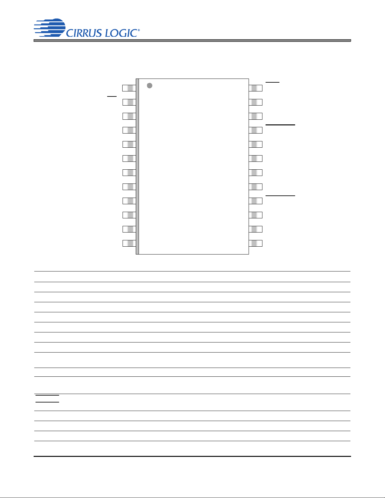
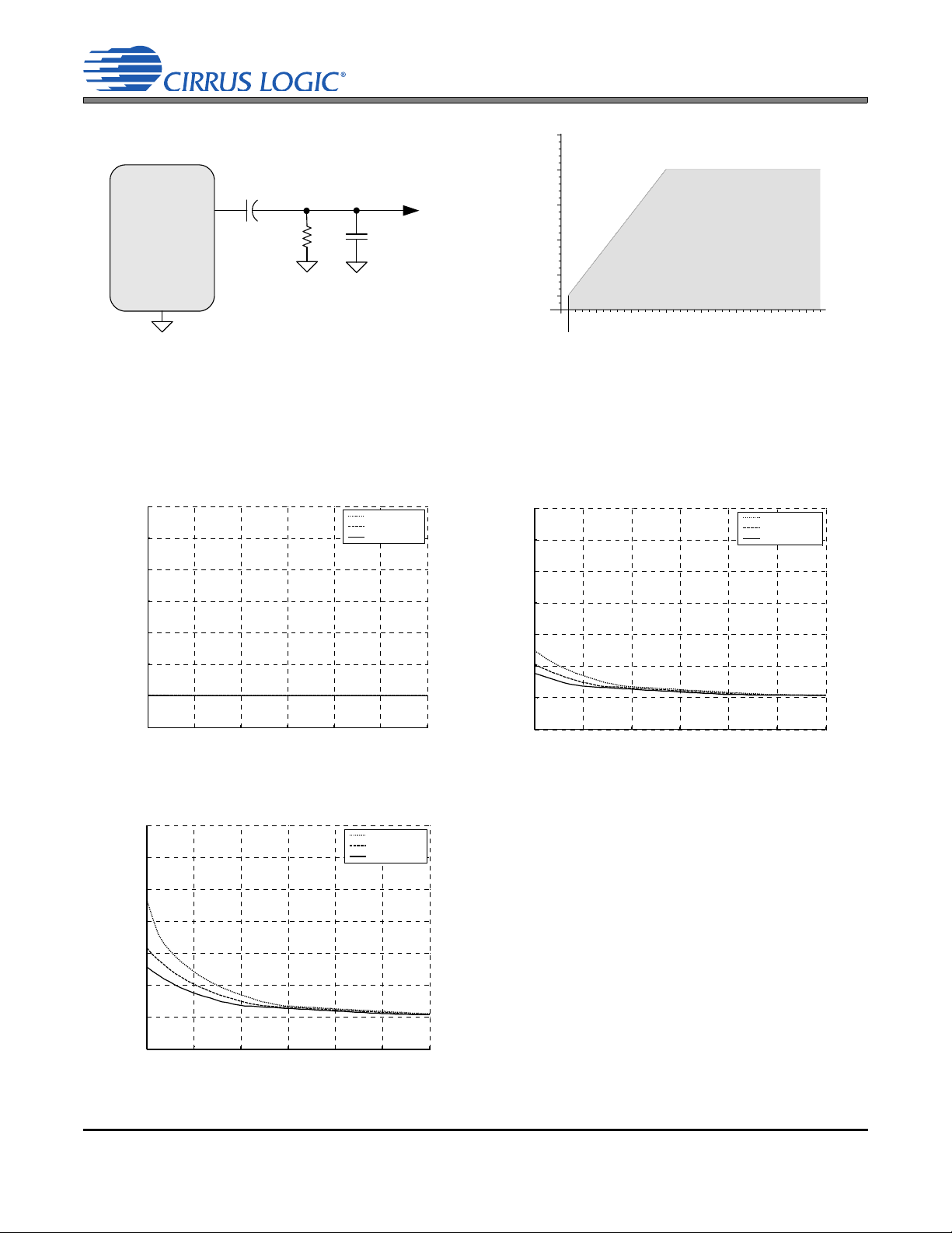
1 PIN DESCRIPTION
DIF2(AD1/CDOUT) RST
DEM(AD0/CS)AOUTB-
DIF0(SDA/CDIN) AOUTB+
DIF1(SCL/CCLK) BMUTEC
VLC VQ
VD_FILT GND
GND VA
RMCK VBIAS+
VLS AMUTEC
SCLK AOUTA+
SDIN AOUTA-
LRCK TSTO
2
3
4
5
6
7
8
17
18
19
20
21
22
23
9
10
11
12
13
14
15
16
24
1
CS4350
Pin Name # Pin Description
VLC
VD_FILT
GND
RMCK
VLS
SCLK
SDIN
LRCK
TSTO 13 Test Output - These pins need to be floating and not connected to any trace or plane.
AOUTA+,AOUTB+,-
AMUTEC
BMUTEC
VBIAS
VA
VQ
14, 15,
6 DS691F2
Control Interface Power (Input) - Positive power for the hardware/software control interface
5
Regulator Voltage (Output) - Filter connection for internal voltage regulator
6
Ground (Input) - Ground reference
7, 19
Recovered Master Clock (Output) - Outputs a master clock derived from LRCK
8
Serial Audio Interface Power (Input) - Positive power for the serial audio interface
9
Serial Clock (Input) - Serial bit-clock for the serial audio interface
10
Serial Audio Data Input (Input) - Input for two’s complement serial audio data
11
Left/Right Clock (Input) - Determines which channel, Left or Right, is currently active on the serial
12
audio data line
Differential Analog Outputs (Output) - The full scale differential output level is specified in “DAC Ana-
log Characteristics - Commercial (-CZZ)” on page 8.
22, 23
16, 21 Mute Control (Output) - Control signals for optional mute circuit.
Positive Voltage Reference (Output) - Positive reference voltage for the internal DAC
17
Analog Power (Input) - Positive power supply for the analog section
18
Quiescent Voltage (Output) - Filter connection for internal quiescent voltage
20
Page 7
Pin Name # Pin Description
RST
Control Port Definitions
AD1/CDOUT
AD0/CS
SDA/CDIN
SCL/CCLK
Stand-Alone Definitions
DIF0
DIF1
DIF2
DEM
Reset (Input) - When pulled low, device will power down and reset all internal registers to their default
24
settings.
1 Address Bit 1/Serial Control Data Out (I/O) - Chip address bit 1 in I²C Mode or data output in SPI Mode
2 Address Bit 0/Chip Select (Input) - Chip address bit 0 in I²C Mode or Chip Select in SPI Mode
3 Serial Control Data In (I/O) - Input/Output for I²C data. Input for SPI data
Serial Control Port Clock (Input) - Serial clock for the control port interface
4
Digital Interface Format (Input) - Defines the required relationship between the Left Right Clock, Serial
1, 3, 4
Clock, and Serial Audio Data
De-emphasis (Input) - Selects the standard 15 s/50 s digital de-emphasis filter response for
2
44.1 kHz sample rates
2 CHARACTERISTICS AND SPECIFICATIONS
2.1 Recommended Operating Conditions
GND = 0 V; all voltages with respect to ground.
Table 1. Recommended Operating Conditions
CS4350
Parameters Symbol Min Typ Max Units
DC Power Supply Analog power VA 4.75 5.0 5.25 V
3.14 3.3 3.46 V
Serial Audio Interface power
Control Interface power
Ambient Operating Temperature (Power Applied)
Commercial (-CZZ) T
Automotive (-DZZ) T
VLS 1.35 3.3 5.25 V
VLC 3.14 3.3 5.25 V
A
A
-40 - +85 °C
-40 - +105 °C
2.2 Absolute Maximum Ratings
GND = 0 V; all voltages with respect to ground (Note 1).
Table 2. Absolute Maximum Ratings
Parameters Symbol Min Max Units
DC Power Supply Analog power VA -0.3 6.0 V
Serial Audio Interface power
Control Interface power
Input Current (Note 2) I
Digital Input Voltage Serial Audio Interface V
Control Interface V
Ambient Operating Temperature (power applied) T
Storage Temperature T
Notes: 1. Operation beyond these limits may result in permanent damage to the device.
Normal operation is not guaranteed at these extremes.
2. Any pin except supplies.
VLS -0.3 6.0 V
VLC -0.3 6.0 V
in
IN-LS
IN-LC
A
stg
-±10mA
-0.3 VLS+ 0.4 V
-0.3 VLC+ 0.4 V
-55 125 °C
-65 150 °C
DS691F2 7
Page 8
CS4350
2.3 DAC Analog Characteristics - Commercial (-CZZ)
Test conditions (unless otherwise specified): VLS = VLC = 3.3 V; TA = 25° C; Input test signal is a 997 Hz
sine wave; Valid with the recommended capacitor values on VD_FILT, VQ, VBIAS (as shown in the typical
connection diagram in Figure 10) and output circuits as shown in Figure 17 and Figure 18; Fs = 48 kHz,
96 kHz, and 192 kHz; measurement bandwidth 10 Hz to 20 kHz.
Table 3. DAC Analog Characteristics - Commercial (-CZZ)
Parameter Symbol Min Typ Max Unit
VA= 5.0 V Single-ended/Differential
Dynamic Range (Note 3) 24-bit A-Weighted
unweighted
16-bit A-Weighted
unweighted
Total Harmonic Distortion + Noise (Note 3)
24-bit 0 dB
-20 dB
-60 dB
16-bit 0 dB
-20 dB
-60 dB
THD+N
VA= 3.3 V Single-ended/Differential
Dynamic Range (Note 3) 24-bit A-Weighted
unweighted
16-bit A-Weighted
unweighted
Total Harmonic Distortion + Noise (Note 3)
24-bit 0 dB
-2 dB
-20 dB
-60 dB
16-bit 0 dB
-20 dB
-60 dB
THD+N
VA= 3.3 to 5.0 V
Interchannel Isolation (1 kHz) - 100 - dB
DC Accuracy
Interchannel Gain Mismatch - 0.1 0.25 dB
Gain Drift - -400 - ppm/°C
Analog Output
Full Scale Output Voltage - Single Ended 2.61 2.78 2.96 Vpp
Full Scale Output Voltage - Differential 5.22 5.56 5.92 Vpp
Quiescent Voltage V
Max DC Current draw from an AOUT pin I
Max Current draw from VQ I
Max AC-Load Resistance (Note 4) R
Max Load Capacitance (Note 4) C
Output Impedance Z
Q
OUTmax
Qmax
L
L
OUT
Notes: 3. One LSB of triangular PDF dither is added to data
4. R
and CL represent the minimum resistance and maximum capacitance required for the CS4350’s in-
L
ternal op-amp to remain stable. See Figure 1 and Figure 2 for more details.
98/106
95/103
-
-
-
-
-
-
-
-
-
98/106
95/103
-
-
-
-
-
-
-
-
-
-0.5•VA-VDC
-10-A
-100-A
-3-k
-100-pF
-100-
101/109
98/106
95/96
92/93
-91
-78/-86
-38/-46
-90
-72/-73
-32/-33
101/109
98/106
95/96
92/93
-86
-91/-93
-78/-86
-38/-46
-83
-72/-73
-32/-33
-
-
-
-
-86/-87
-
-35/-43
-
-
-
-
-
-
-
-77
-
-
-35/-43
-
-
-
dB
dB
dB
dB
dB
dB
dB
dB
dB
dB
dB
dB
dB
dB
dB
dB
dB
dB
dB
dB
dB
8 DS691F2
Page 9

CS4350
2.4 DAC Analog Characteristics - Automotive (-DZZ)
Test conditions (unless otherwise specified): VLS = 1.35 V to 5.25 V, VLC = 3.14 V to 5.25 V, TA = -40° C
to 105° C, input test signal is a 997 Hz sine wave; Valid with the recommended capacitor values on VFILT,
VQ, VBIAS (as shown in the typical connection diagram in Figure 10) and output circuits as shown in
Figure 17 and Figure 18; Fs = 48 kHz, 96 kHz, and 192 kHz; Measurement bandwidth 10 Hz to 20 kHz.
Table 4. DAC Analog Characteristics - Automotive (-DZZ)
Parameter Symbol Min Typ Max Unit
VA= 4.75 V to 5.25 V Single-ended/Differential
Dynamic Range (Note 3) 24-bit A-Weighted
unweighted
16-bit A-Weighted
unweighted
Total Harmonic Distortion + Noise (Note 3)
24-bit 0 dB
-20 dB
-60 dB
16-bit 0 dB
-20 dB
-60 dB
THD+N
VA= 3.14 V to 3.46 V Single-ended/Differential
Dynamic Range (Note 3) 24-bit A-Weighted
unweighted
16-bit A-Weighted
unweighted
Total Harmonic Distortion + Noise (Note 5)
24-bit -1 dB
-2 dB
-20 dB
-60 dB
16-bit 0 dB
-20 dB
-60 dB
THD+N
VA= 3.14 to 5.25 V
Interchannel Isolation (1 kHz) - 100 - dB
DC Accuracy
Interchannel Gain Mismatch - 0.1 0.25 dB
Gain Drift - -400 - ppm/°C
Analog Output
Full Scale Output Voltage - Single Ended 2.55 2.78 3.03 Vpp
Full Scale Output Voltage - Differential 5.10 5.56 6.06 Vpp
Quiescent Voltage V
Max DC Current draw from an AOUT pin I
Max Current draw from VQ I
Max AC-Load Resistance (Note 4) R
Max Load Capacitance (Note 4) C
Output Impedance Z
Q
OUTmax
Qmax
L
L
OUT
Note: 5. One-half LSB of triangular PDF dither is added to data. Also, see Figure 3, Figure 4, and Figure 5 for
more details on the CS4350-DZZ THD+N performance with 0dB input signal.
95/103
92/100
-
-
-
-
-
-
-
-
-
94/103
91/100
-
-
-
-
-
-
-
-
-
-0.5•VA-VDC
-10-A
- 100 - A
-3-k
- 100 - pF
- 100 -
101/109
98/106
95/96
92/93
-91
-78/-86
-38/-46
-90
-72/-73
-32/-33
101/109
98/106
95/96
92/93
-89
-91/-93
-78/-86
-38/-46
-83
-72/-73
-32/-33
-
-
-
-
-85
-
-32/-40
-
-
-
-
-
-
-
-83
-
-
-31/-40
-
-
-
dB
dB
dB
dB
dB
dB
dB
dB
dB
dB
dB
dB
dB
dB
dB
dB
dB
dB
dB
dB
dB
DS691F2 9
Page 10
CS4350
AOUTx
3.3 µF
Analog
Output
+
CS4350
GND
R
L
C
L
100
50
75
25
2.5
51015
Safe Operating
Region
Capacitive Load -- C (pF)
L
Resistive Load -- R (k)
L
125
3
20
Figure 1. Equivalent Output Load Figure 2. Maximum Loading
-3-2.5-2-1.5-1-0.50
-100
-90
-80
-70
-60
-50
-40
-30
Output A mplitude(d B)
THD+N (dB)
TA = -40° C
TA = 25° C
TA = 85° C
-3-2.5-2-1.5-1-0.50
-100
-90
-80
-70
-60
-50
-40
-30
Output Amplitude(dB)
THD+N (dB)
TA = -40° C
TA = 25° C
TA = 85° C
Figure 3. THD+N vs Output Amplitude for VA = 5.0 V Figure 4. THD+N vs Output Amplitude for VA = 3.3 V
-3-2.5-2-1.5-1-0.50
-100
-90
-80
-70
-60
-50
-40
-30
Output Amplitude(dB)
THD+N (dB)
TA = -40° C
TA = 25° C
TA = 85° C
Figure 5. THD+N vs Output Amplitude for VA = 3.14 V
Figures 3 through 5 show typical THD+N performance for CS4350 devices that exhibit the maximum full scale output voltages as specified in the DAC Analog Characteristics tables (see page 8 and 9). With decreasing VA,
THD+N performance is increasingly affected by the full scale output voltage and temperature, with higher full scale
output voltage and lower temperatures corresponding to lower THD+N performance.
10 DS691F2
Page 11
CS4350
2.5 Combined Interpolation and On-Chip Analog Filter Response
The filter characteristics have been normalized to the sample rate (Fs) and is referenced to the desired sample rate by multiplying the given characteristic by Fs. Amplitude vs. Frequency plots of this data are available
in the “Filter Plots” on page 35.
Table 5. Combined Interpolation and On-Chip Analog Filter Response
Parameter Min Typ Max Unit
Fast Roll-Off
Passband (Note 6) -0.01 dB corner (Single Speed) 0 - .454 Fs
-0.1 dB corner (Double Speed) 0 - .42 Fs
-0.2 dB corner (Quad Speed) 0 - .27 Fs
-3 dB corner (All Speed Modes) 0 - .499 Fs
Frequency Response 10 Hz to 20 kHz Single Speed -0.01 - +0.01 dB
Double Speed, Quad Speed -0.02 - +0.02 dB
StopBand 0.547 - - Fs
Stop-Band Attenuation (Note 7) 102 - - dB
Total Group Delay (Fs - Output Sample Rate) TDM Slot 0 Channel B - 8.4/Fs - s
All Other Interface Formats and TDM Slots/Channels - 9.4/Fs - s
Intrachannel Phase Deviation - - ±0.56/Fs s
Interchannel Phase Deviation - - 0 s
De-emphasis Error (Note 8) Fs = 32 kHz - - ±0.23 dB
(Relative to 1 kHz) Fs = 44.1 kHz - - ±0.14 dB
Fs = 48 kHz
Slow Roll-Off (Note 9)
Passband (Note 6) -0.01 dB corner (Single Speed) 0 - 0.417 Fs
-0.1 dB corner (Double Speed) 0 - .37 Fs
-0.2 dB corner (Quad Speed) 0 - .27 Fs
-3 dB corner (All Speed Modes) 0 - .499 Fs
Frequency Response 10 Hz to 20 kHz Single Speed -0.01 - +0.01 dB
Double Speed, Quad Speed -0.02 - +0.02 dB
StopBand .583 - - Fs
Stop-Band Attenuation (Note 7) 64 - - dB
Total Group Delay (Fs - Output Sample Rate) TDM Slot 0 Channel B - 5.5/Fs - s
All Other Interface Formats and TDM Slots/Channels - 6.5/Fs - s
Intrachannel Phase Deviation - - ±0.14/Fs s
Interchannel Phase Deviation - - 0 s
De-emphasis Error (Note 8) Fs = 32 kHz - - ±0.23 dB
(Relative to 1 kHz) Fs = 44.1 kHz - - ±0.14 dB
Fs = 48 kHz
--±0.09dB
--±0.09dB
Notes: 6. Response is clock dependent.
7. The Measurement Bandwidth is from stopband to 3 Fs.
8. De-emphasis is available only in Single-Speed Mode; Only 44.1 kHz De-emphasis is available in StandAlone Mode.
9. Slow Roll-off interpolation filter is only available in Control Port Mode.
DS691F2 11
Page 12
CS4350
2.6 Switching Specifications - Serial Audio Interface
Inputs: Logic 0 = GND; Logic 1 = VLS; CL=20pF.
Table 6. Switching Specifications - Serial Audio Interface
Parameters Symbol Min Max Units
3.14 V
RMCK Output Frequency (Note 10) 7.680 55.3 MHz
RMCK Output Duty Cycle 45 55 %
Input Sample Rate Single-Speed Mode 30 54
LRCK Duty Cycle (Non-TDM Mode) 40 60 %
SDIN Setup Time Before SCLK Rising Edge t
SDIN Hold Time After SCLK Rising Edge t
4.75 V VA 5.25 V and 3.14 V VLS 5.25 V
SCLK Frequency -55.3MHz
SCLK High Time t
SCLK Low Time t
Non-TDM Mode (refer to Figure 6)
LRCK Edge to SCLK Rising Edge t
SCLK Rising Edge to LRCK Edge t
TDM Mode (refer to Figure 7)
LRCK High Time t
SCLK Rising to LRCK Falling Edge t
LRCK Rising Edge to SCLK Rising Edge t
SCLK Frequency -27.7MHz
SCLK High Time t
SCLK Low Time t
Non-TDM Mode (refer to Figure 6)
LRCK Edge to SCLK Rising Edge t
SCLK Rising Edge to LRCK Edge t
TDM Mode (refer to Figure 7)
LRCK High Time t
SCLK Rising to LRCK Falling Edge t
LRCK Rising Edge to SCLK Rising Edge t
VA 5.25 V and 1.35 V VLS 5.25 V
Double-Speed Mode Fs 60 108 kHz
Quad-Speed Mode 120 216
ds
dh
sckh
sckl
lcks
lckd
lrckh
fsh
fss
3.14 V VA < 4.75 V or 1.35 V VLS < 3.14 V
sckh
sckl
lcks
lckd
lrckh
fsh
fss
1-ns
1-ns
6-ns
6-ns
11 - n s
1-ns
6-ns
3-ns
1-ns
11 - n s
11 - n s
16 - ns
1-ns
25 - ns
8-ns
1-ns
Note: 10. RMCK output frequency depends on the input LRCK frequency. See Section 4.1 and Section 4.2 for
more details.
12 DS691F2
Page 13

2.7 Switching Characteristics - Control Port - I²C Format
t
ds
LRCK
(Input)
t
dh
t
sckh
t
sckl
t
fsh
t
fss
SCLK
(Input)
SDIN
(Input)
MSB
MSB-1
t
lrckh
t
ds
MSB
t
dh
MSB-1
LRCK
(input)
SCLK
(input)
SDIN
(input)
t
sckh
t
sckl
t
lcks
t
lckd
Figure 6. Serial Port Timing, Non-TDM Mode Figure 7. Serial Port Timing, TDM Mode
t
buf
t
hdst
t
low
t
hdd
t
high
t
sud
Stop S ta rt
SDA
SCL
t
irs
RST
t
hdst
t
rc
t
fc
t
sust
t
susp
Start
Stop
Repeated
t
rd
t
fd
t
ack
Figure 8. Control Port Timing - I²C Format
Inputs: Logic 0 = GND; Logic 1 = VLC; CL=20pF.
Table 7. Switching Characteristics - Control Port - I²C Format
Parameter Symbol Min Max Unit
SCL Clock Frequency f
RST
Rising Edge to Start t
Bus Free Time Between Transmissions t
Start Condition Hold Time (prior to first clock pulse) t
Clock Low time t
Clock High Time t
Setup Time for Repeated Start Condition t
SDA Hold Time from SCL Falling (Note 11) t
SDA Setup time to SCL Rising t
Rise Time of SCL and SDA t
Fall Time SCL and SDA tfc, t
Setup Time for Stop Condition t
Acknowledge Delay from SCL Falling t
buf
hdst
low
high
sust
hdd
sud
rc
susp
ack
scl
irs
, t
rc
fc
CS4350
- 100 kHz
500 - ns
4.7 - µs
4.0 - µs
4.7 - µs
4.0 - µs
4.7 - µs
0-µs
250 - ns
-1µs
-300ns
4.7 - µs
300 1000 ns
Note: 11. Data must be held for sufficient time to bridge the transition time, t
DS691F2 13
fc
, of SCL.
Page 14

2.8 Switching Characteristics - Control Port - SPI Format
t
r2
t
f2
t
dsu
t
dh
t
sch
t
scl
CS
CCLK
CDIN
t
css
t
csh
t
spi
t
srs
RST
CDOUT
t
scdov
t
scdov
t
cscdo
Hi-Impedance
Inputs: Logic 0 = GND; Logic 1 = VLC; CL=20pF.
Table 8. Switching Characteristics - Control Port - SPI Format
Parameter Symbol Min Max Unit
CCLK Clock Frequency f
RST Rising Edge to CS Falling t
CCLK Edge to CS Falling (Note 12) t
CS
High Time Between Transmissions t
CS Falling to CCLK Edge t
CCLK Low Time t
CCLK High Time t
CDIN to CCLK Rising Setup Time t
CCLK Rising to DATA Hold Time (Note 13) t
Rise Time of CCLK and CDIN (Note 14) t
Fall Time of CCLK and CDIN (Note 14) t
Transition Time from CCLK to CDOUT Valid (Note 15) t
Time from CS
Notes: 12. t
rising to CDOUT High-Z t
only needed before first falling edge of CS after RST rising edge. t
spi
13. Data must be held for sufficient time to bridge the transition time of CCLK.
14. For F
< 1 MHz.
SCK
15. CDOUT should not be sampled during this time.
sclk
srs
spi
csh
css
scl
sch
dsu
dh
r2
f2
scdov
cscdo
CS4350
-6MHz
500 - ns
500 - ns
1.0 - µs
20 - ns
66 - ns
66 - ns
40 - ns
15 - ns
- 100 ns
- 100 ns
- 100 ns
- 100 ns
= 0 at all other times.
spi
Figure 9. Control Port Timing - SPI Mode
14 DS691F2
Page 15

CS4350
2.9 Digital Characteristics
Table 9. Digital Characteristics
Parameters Symbol Min Typ Max Units
High-Level Input Voltage VLC or VLS = 5.0 V V
VLC or VLS = 3.3 V
VLS = 2.5 V
VLS = 1.5 V
High-Level Input Voltage VLC or VLS = 5.0 V V
VLC or VLS = 3.3 V
VLS = 2.5 V
VLS = 1.5 V
Input Leakage Current I
IH
V
IH
V
IH
V
IH
IL
V
IL
V
IL
V
IL
in
Input Capacitance - 8 - pF
High Level Output Voltage (RMCK) I
Low Level Output Voltage (RMCK) I
= 2 mA (VLS 3.0V)
O
= -2 mA (VLS 3.0V)
O
V
OH
V
OL
RMCK Output Load Drive - - 10 pF
Maximum MUTEC Drive Current - 2 - mA
MUTEC High-Level Output Voltage V
MUTEC Low-Level Output Voltage V
OH
OL
0.7•V
L
-- V
2.0 - - V
1.7 - - V
0.75•V
- - 0.35•V
-- V
L
L
--0.8V
--0.7V
- - 0.25•V
L
--±10A
VLS-1.0 - - V
--0.4V
-VA- V
-0- V
V
V
2.10 Power and Thermal Characteristics
Table 10. Power and Thermal Characteristics
Parameters Symbol Min Typ Max Units
Power Supply Current - Normal Operation (Note 16) VA= 5 . 0 V I
VA= 3 . 3 V I
= VLC =5.0 V (Note 17) I
VLS
= VLC =3.3 V (Note 17) I
VLS
= VLC = 5.0 V (Note 18) I
VLS
VLS
= VLC = 3.3 V (Note 18) I
A
A
LS
LS
LC
LC
Power Supply Current - Power-Down State (Note 19)
VA, V L S
VLC I
,
pd
Power Dissipation - Normal Operation (Note 16)
VA = VLC= VLS = 5.0 V - 230 290 mW
VA = VLC= VLS = 3.3 V - 132 171 mW
Power Dissipation - Power-Down State (Note 19)
VA = VLC= VLS = 5.0 V - 0.5 - mW
VA = VLC= VLS = 3.3 V - 0.33 - mW
Power Supply Rejection Ratio (Note 20) (1 kHz) PSRR - 60 - dB
(60 Hz) PSRR - 50 - dB
Notes: 16. Current consumption increases with increasing Fs within the range of a speed mode. Variance between
speed modes is small. Typ and Max values are based on Fs = 48 kHz.
17. I
18. I
19. Power-down mode is defined as RST
measured with no external loading on pin 7 (RMCK).
LS
measured with no external loading on pin 2 (SDA).
LC
pin = Low with all clock and data lines held static.
20. Valid with the recommended capacitor values on VFILT, VQ, and VBIAS+ as shown in the typical connection diagram in Figure 10.
-2834mA
-2429mA
-46mA
-25mA
-1418mA
-1418mA
- 100 - A
DS691F2 15
Page 16

3 TYPICAL CONNECTION DIAGRAM
Digital
Audio
Source
VLS
G
ND
CS4350
RMCK
AOUTA+
0.1 µF
+
10 µF
µ C/
Mode
Configuration
SDIN
DIF1(SCL/CCLK)
DIF0(SDA/CDIN)
3.3 µF
AOUTA
+
VBIAS+
VQ
LRCK
SCLK
AOUTB+
10 µF
VD_FILT
GN
D
0.1 µF
+1.5 V to +5 V
V
A
0.1 µF
10 µF
+3.3 V or +5 V
VLC
0.1 µF
+3.3 V to +5 V
47 k
AOUTA-
AOUTB-
DIF2(AD1/CDOUT)
Differential or Single-
ended Output Filter
AOUTB
T
S
TO
Differential or Single-
ended Output Filter
+
+
8
12
10
11
9
5
24
RST
4
3
2
DEM(AD0/CS)
1
13
7
19
20
23
22
21
BMUTEC
14
15
16
AMUTEC
6
17
18
N.C.
VLS = PopGuard Enable
GND = PopGuard Disable
Figure 10. Typical Connection Diagram
CS4350
16 DS691F2
Page 17

4 APPLICATIONS
4.1 Sample Rate Range and Oversampling Mode Detect
The device operates in one of three oversampling modes based on the input sample rate. In Control Port
Mode, the allowed sample rate range in each mode will depend on how the FM[1:0] bits are configured. In
Stand-Alone Mode, the sample rate range will be according to Table 11.
4.1.1 Sample Rate Auto-Detect
The Auto-Detect feature is enabled by default. In this state, the CS4350 will auto-detect the correct mode
when the input sample rate (Fs), defined by the LRCK frequency, falls within one of the ranges shown in
Table 11. Sample rates outside the specified range for each mode are not supported when Auto-Detect
is enabled.
Table 11. CS4350 Auto-Detect
Input Sample Rate (Fs) Mode
30 kHz - 54 kHz Single-Speed Mode
60 kHz - 108 kHz Double-Speed Mode
120 kHz - 216 kHz Quad-Speed Mode
In Control Port Mode, the Auto-Detect feature can be disabled by the Functional Mode (FM[1:0]) bits in
the control port register 02h. In this state, the CS4350 will not auto-detect the correct mode based on the
input sample rate (Fs). The operational mode must then be set manually according to one of the ranges
referred to in Section 8.2.3. Sample rates outside the specified range for each mode are not supported.
In Stand-Alone Mode it is not possible to disable auto-detect of sample rates.
CS4350
4.2 System Clocking
The device requires external generation of the left/right (LRCK) and serial (SCLK) clocks. The left/right clock
frequency is equal to the input sample rate (Fs).
Refer to Section 4.3 for the required SCLK-to-LRCK timing associated with the selected digital interface format, and “Switching Specifications - Serial Audio Interface” on page 12 for the maximum allowed clock fre-
quencies.
4.2.1 Recovered Master Clock (RMCK)
The CS4350 generates a high-frequency master clock (RMCK) which it derives from the LRCK input,
available on the RMCK pin. In Stand-Alone Mode, the frequency of RMCK is equal to 256 x LRCK in Single-Speed and Double-Speed Mode; and 128 x LRCK in Quad-Speed Mode. In Control-Port Mode, the
frequency of the RMCK signal can be selected through register 08h (see Section 8.7 on page 33 for more
details).
DS691F2 17
Page 18

4.3 Digital Interface Format
+3 +2 +1+5 +4
MSB
-1 -2 -3 -4 -5
+3 +2 +1+5 +4
-1 -2 -3 -4
LSB
MSB
LSB
Left Channel Right Channel
LRCK
SCLK
SDIN
Figure 11. Left-Justified up to 24-Bit Data
+3 +2 +1+5 +4
MSB
-1 -2 -3 -4 -5
+3 +2 +1+5 +4
-1 -2 -3 - 4
MSB
LSB
LSB
Left Channel
Right Channel
LRCK
SCLK
SDIN
Figure 12. I²S, up to 24-Bit Data
SDIN
+6 +5 +4 +3 +2 +1+7
-1 -2 -3 -4
-5
LSB
LSBMSB
-1 -2 -3 -4
-5
LSB
+6 +5 +4 +3 +2 +1+7
MSB
Left Channel
Right Channel
LRCK
SCLK
Figure 13. Right-Justified Data
The device will accept audio samples in 1 of 8 digital interface formats, as shown in Table 12 on page 23
for Stand-Alone Mode and Table 13 on page 28 for Control Port Mode.
The desired serial audio interface format is selected via the DIF[2:0] bits in Control Port Mode (see
Section 8.2.1), or the DIF[2:0] pins in Stand-Alone Mode (see Section 5.1). For illustrations of the required
relationship between LRCK, SCLK and SDIN, see Figures 11-13. For all formats, SDIN is valid on the rising
edge of SCLK.
For more information about serial audio formats, refer to the Cirrus Logic Application Note AN282,
The 2-Channel Serial Audio Interface: A Tutorial, available at www.cirrus.com.
CS4350
18 DS691F2
Page 19

4.3.1 Time-Division Multiplex (TDM) Mode
LRCK
SCLK
SDIN
ILRCK
ISCLK
SDIN
LRCK
SCLK
SDIN
LRCK SCLK TDM_OUT
TDM Source
CS4350
1
CS4350
2
LRCK
SCLK
SDIN
CS4350
3
DIF[2:0] = 100 DIF[2:0] = 101 DIF[2:0] = 110 DIF[2:0] = 111
CS4350
4
Figure 14. TDM Mode Connection Diagram
Slot 1, ch B
LRCK
SCLK
MSB MSB MSB MSB MSB
SDIN1
Slot 3, ch A Slot 3, ch B
Slot 1, ch ASlot 0, ch A
256 clks
32 clks 32 clks 32 clks 32 clks 32 clks
MSB
Slot 2, ch A
32 clks
MSB
Slot 0, ch B
32 clks
MSB
Slot 2, ch B
32 clks
LSBMSB
zero
Data
Figure 15. TDM Mode Timing
Four TDM interface modes are available that allow the CS4350 to input stereo PCM data in one of 4 time
“slots”. Figure 14 shows the serial port connections necessary to input 8-channel TDM data into four
CS4350 devices, and the corresponding DIF[2:0] pin or register-bit settings required for each CS4350.
Figure 15 shows the TDM data format for each of the four CS4350 devices shown in Figure 14.
Note: The group delay for TDM slot 0 channel B differs from the group delay of all other interface for-
mats and TDM slots/channels by one sample. Refer to the group delay specification in the combined interpolation and on-chip analog filter response specifications table.
.
CS4350
DS691F2 19
Page 20

4.4 De-Emphasis
Gain
dB
-10dB
0dB
Frequency
T2 = 15 µs
T1=50 µs
F1 F2
3.183 kHz 10.61 kHz
Figure 16. De-Emphasis Curve
The device includes on-chip digital de-emphasis. Figure 16 shows the de-emphasis curve for Fs equal to
44.1 kHz. The frequency response of the de-emphasis curve will scale proportionally with changes in sample rate, Fs.
Note: De-emphasis is only available in Single-Speed Mode.
4.5 Mute Control
CS4350
The mute control pins (AMUTEC and BMUTEC) go active during power-up initialization, reset, muting (see
Section 8.4.3), and loss of LRCK. These pins are intended to be used as control for external mute circuits
to prevent the clicks and pops that can occur in any single-ended single-supply system.
Use of the mute control function is not mandatory but recommended for designs requiring the absolute minimum in extraneous clicks and pops. Also, use of the Mute Control function can enable the system designer
to achieve idle-channel noise and signal-to-noise ratios which are only limited by the external mute circuit.
4.6 Recommended Power-Up Sequence
4.6.1 Stand-Alone Mode
1. Hold RST low until the power supplies and configuration pins are stable and the left/right clock is fixed
to the appropriate frequencies, as discussed in Section 4.2. In this state, the control port registers are
reset to their default settings, VQ will remain low, and VBIAS will be connected to VA.
2. Bring RST
cycles in Single-Speed Mode (384 LRCK cycles in Double-Speed Mode, and 768 LRCK cycles in
Quad-Speed Mode).
3. The device will then initiate the power up sequence which lasts approximately 130 ms when the
Popguard is disabled. If the Popguard is enabled, see Section 4.7 for a complete description of
power-up timing.
high. The device will remain in a low power state with VQ low for approximately 192 LRCK
20 DS691F2
Page 21

4.6.2 Control Port Mode
1. Hold RST low until the power supply is stable and the left/right clock is fixed to the appropriate
frequency, as discussed in Section 4.2. In this state, the control port is reset to its default settings, VQ
will remain low, and VBIAS will be connected to VA.
CS4350
2. Bring RST
3. Perform a control port write to a valid register prior to the completion of approximately 192 LRCK
cycles in Single-Speed Mode (384 LRCK cycles in Double-Speed Mode, and 768 LRCK cycles in
Quad-Speed Mode). The desired register settings can be loaded while keeping the PDN bit set to 1.
4. Set the PDN bit to 0. This will initiate the power-up sequence, which lasts approximately 130 ms when
the Popguard is disabled. If the Popguard is enabled, see Section 4.7 for a complete description of
power-up timing.
high. The device will remain in a low-power state with VQ low.
4.7 Popguard Transient Control
The CS4350 uses a novel technique to minimize the effects of output transients during power-up and powerdown. This technology, when used with external DC-blocking capacitors in series with the audio outputs,
minimizes the audio transients commonly produced by single-ended single-supply converters. It is activated
inside the DAC when the RST
appropriate DC-blocking capacitors.
pin is toggled and requires no other external control, aside from choosing the
4.7.1 Power-Up
When the device is initially powered-up, the audio outputs, AOUTA and AOUTB, are clamped to GND.
Following a delay of approximately 192 sample periods, each output begins to ramp toward the quiescent
voltage. The amount of time it takes the outputs to ramp is related to the value of the DC-blocking capacitance and the output load. Using the example output circuit from Figure 18, the ramp up time will be approximately 0.25 seconds. When the ramp is complete, the outputs reach V
This gradual voltage ramping allows time for the external DC-blocking capacitors to charge to the quiescent voltage, minimizing audible power-up transients.
and audio output begins.
Q
Note the ramp up time will vary due to internal factors such as variance across device process, supply
voltage, and die temperature corners as well as external output circuit component tolerances.
4.7.2 Power-Down
To prevent audible transients at power-down, the device must first enter its power-down state. When this
occurs, audio output ceases and the internal output buffers are disconnected from AOUTA and AOUTB.
In their place, a soft-start current sink is substituted which allows the DC-blocking capacitors to slowly discharge. Once this charge is dissipated, the power to the device may be turned off, and the system is ready
for the next power-on.
4.7.3 Discharge Time
To prevent an audio transient at the next power-on, the DC-blocking capacitors must fully discharge before turning on the power or exiting the power-down state. If full discharge does not occur, a transient will
occur when the audio outputs are initially clamped to GND. The time that the device must remain in the
power-down state is related to the value of the DC-blocking capacitance and the output load. For example,
with a 3.3 µF capacitor, the minimum power-down time will be approximately 0.2 seconds.
DS691F2 21
Page 22

4.8 Analog Output and Filtering
AOUTx +
AOUTx -
-
+
1000 pF
C0G
562
22 F
4.02 k
5600 pF
C0G
221
392 4.64 k
1.62 k
1.37 k
22 F
2700 pF
C0G
.015 F
C0G
47 k
CS4350
GND
Analog
Output
* See section 4.9 for ground connection details
Figure 17. Differential to Single-Ended Output Filter
AOUTx +
3.3 µF
Analog
Output
2200 pF
+
10 k
CS4350
GND
560
* See section 4.9 for ground connection details
Figure 18. Passive Single-Ended Output Filter
The Cirrus Application Note titled Design Notes for a 2-Pole Filter with Differential Input, available as AN48
at www.cirrus.com, discusses the second-order Butterworth filter and differential-to-single-ended converter
that was implemented on the CS4350 evaluation board, CDB4350. Figure 17 illustrates this
implementation. If only single-ended outputs from the CS4350 are required, the passive output filter shown
in Figure 18 can be used.
CS4350
4.9 Grounding and Power Supply Arrangements
As with any high-resolution converter, the CS4350 requires careful attention to power supply and grounding
arrangements if its potential performance is to be realized. Figure 10 shows the recommended power arrangements, with VA, VLC, and VLS connected to clean supplies. The use of split analog and digital ground
planes is not recommended. However, if planes are split between digital ground and analog ground the
GND pins of the CS4350 should be connected to the analog ground plane.
All signals, especially clocks, should be kept away from the VBIAS, VFILT, and VQ pins in order to avoid
unwanted coupling into the DAC.
4.9.1 Capacitor Placement
Decoupling capacitors should be placed as close to the DAC as possible, with the low value ceramic capacitor being the closest. To further minimize impedance, these capacitors should be located on the same
layer as the DAC. If desired, all supply pins may be connected to the same supply, but a decoupling capacitor should still be placed on each supply pin.
22 DS691F2
Note: All decoupling capacitors should be referenced to GND.
The CDB4350 evaluation board demonstrates the optimum layout and power supply arrangements.
Page 23

5 STAND-ALONE OPERATION
5.1 Serial Port Format Selection
The desired serial audio format is selected with the DIF2, DIF1 and DIF0 pins. For an explanation of the
required relationship between the LRCK, SCLK and SDIN, see Figures 11-13. For all formats, SDIN is valid
on the rising edge of SCLK. TDM Mode requires the selection of which stereo pair time “slot” is used to output data as shown in Table 12 and Figure 15.
Note: The group delay for TDM slot 0 channel B differs from the group delay of all other interface formats
and TDM slots/channels by one sample. Refer to the group delay specification in the combined interpolation and on-chip analog filter response specifications table.
DIF2 DIF1 DIF0 DESCRIPTION FORMAT FIGURE
000
001
010
011
100
101
110
111
Table 12. Digital Interface Format - Stand-Alone Mode
Left-Justified, up to 24-bit data
I²S, up to 24-bit data
Right-Justified, 16-bit data
Right-Justified, 24-bit data
TDM slot 0
TDM slot 1
TDM slot 2
TDM slot 3
CS4350
0 12
1 11
2 13
3 13
4 15
5 15
6 15
7 15
5.2 De-Emphasis Control
When pulled to VLC, the DEM pin activates the 44.1 kHz de-emphasis filter. When pulled to GND, the DEM
pin turns off the de-emphasis filter.
5.3 Popguard Transient Control
In Stand-Alone Mode, Popguard is selected by placing a 47 k resistor between RMCK and VLS. Popguard
is defeated in Stand-Alone Mode by placing a 47 k resistor between RMCK and ground.
6 CONTROL PORT OPERATION
The control port is used to load all the internal register settings (see ”Register Description” on page 28). The operation of the control port may be completely asynchronous with the audio sample rate. However, to avoid potential
interference problems, the control port pins should remain static if no operation is required.
The control port can operate in I²C or SPI mode.
6.1 MAP Auto Increment
The device has a MAP (memory address pointer) auto-increment capability enabled by the INCR bit (also
the MSB) of the MAP. If INCR is set to 0, MAP will stay constant for consecutive writes or reads. If INCR is
set to 1, MAP will auto increment after each byte is read or written, allowing block reads or writes of consecutive registers.
6.2 I²C Mode
In the I²C Mode, data is clocked into and out of the bi-directional serial control data line, SDA, by the serial
control port clock, SCL (see Figure 19 for the clock to data relationship). There is no CS
DS691F2 23
pin. AD1 and AD0
Page 24

enable the user to alter the chip address (10010[AD1][AD0][R/W]) and should be tied to VLC or GND as
required before powering up the device. SPI Mode will be selected if the device ever detects a high to low
transition on the AD0/CS
6.2.1 I²C Write
To write to the device, follow the procedure below while adhering to the control port Switching Specifications in ”Switching Characteristics - Control Port - I²C Format” on page 13.
1. Initiate a START condition to the I²C bus followed by the address byte. The upper 5 bits must be
10010. The sixth and seventh bit must match the settings of the AD1 and AD0 pins respectively, and
the eighth must be 0 (the eighth bit of the address byte is the R/W
2. Wait for an acknowledge (ACK) from the part, then write to the memory address pointer, MAP. This
byte points to the register to be written.
3. Wait for an acknowledge (ACK) from the part, then write the desired data to the register pointed to by
the MAP.
4. If the INCR bit (see Section 6.1) is set to 1, repeat the previous step until all the desired registers are
written, then initiate a STOP condition to the bus.
5. If the INCR bit is set to 0 and further I²C writes to other registers are desired, it is necessary to initiate
a repeated START condition and follow the procedure detailed from step 1. If no further writes to other
registers are desired, initiate a STOP condition to the bus.
CS4350
pin after power-up.
bit).
6.2.2 I²C Read
To read from the device, follow the procedure below while adhering to the control port switching specifications in ”Switching Characteristics - Control Port - I²C Format” on page 13.
1. Initiate a START condition to the I²C bus followed by the address byte. The upper 5 bits must be
10010. The sixth and seventh bits must match the setting of the AD1 and AD0 pins, respectively, and
the eighth must be 1. The eighth bit of the address byte is the R/W
2. After transmitting an acknowledge (ACK), the device will then transmit the contents of the register
pointed to by the MAP. The MAP register will contain the address of the last register written to the
MAP or the default address (see Section 6.4.2) if an I²C read is the first operation performed on the
device.
3. Once the device has transmitted the contents of the register pointed to by the MAP, issue an ACK.
4. If the INCR bit is set to 1, the device will continue to transmit the contents of successive registers.
Continue providing a clock and issue an ACK after each byte until all the desired registers are read;
then initiate a STOP condition to the bus.
5. If the INCR bit is set to 0 and further I²C reads from other registers are desired, it is necessary to
initiate a repeated START condition and follow the procedure detailed from steps 1 and 2 from the I²C
Write instructions, followed by step 1 of the I²C Read section. If no further reads from other registers
are desired, initiate a STOP condition to the bus.
bit.
24 DS691F2
Page 25

4 5 6 7 24 25
SCL
CHIP ADDRESS MAP BYTE DATA
DATA +1
START
ACK
STOP
ACKACKACK
1 0 0 1 0 AD1 AD0 R/W
SDA
6 5 4 3 2 1 0
7 6 1 0 7 6 1 0 7 6 1 0
0 1 2 3 8 9 12 16 17 18 19 10 11 13 14 15 27 28
26
DATA +n
INC
Figure 19. Control Port Timing, I²C Mode
6.3 SPI Mode
In SPI Mode, data is clocked into the serial control data line, CDIN, by the serial control port clock, CCLK
(see Figure 20 for the clock to data relationship). There are no AD0 or AD1 pins. Pin CS
signal and is used to control SPI writes to the control port. When the device detects a high-to-low transition
on the AD0/CS
on the rising edge of CCLK.
6.3.1 SPI Write
To write to the device, follow the procedure below while adhering to the control port switching specifications in ”Switching Characteristics - Control Port - SPI Format” on page 14.
CS4350
is the chip select
pin after power-up, SPI Mode will be selected. All signals are inputs and data is clocked in
1. Bring CS
2. The address byte on the CDIN pin must then be 10011110 (R/W
3. Write to the memory address pointer, MAP. This byte points to the register to be written.
4. Write the desired data to the register pointed to by the MAP.
5. If the INCR bit (see Section 6.1) is set to 1, repeat the previous step until all the desired registers are
written, then bring CS
6. If the INCR bit is set to 0 and further SPI writes to other registers are desired, it is necessary to bring
CS
high, and follow the procedure detailed from step 1. If no further writes to other registers are
desired, bring CS
6.3.2 SPI Read
To read from the device, follow the procedure below while adhering to the values specified in ”Switching
Characteristics - Control Port - SPI Format” on page 14.
1. Bring CS
2. The address byte on the CDIN pin must then be 10011111 (R/W
3. CDOUT pin will then output the data from the register pointed to by the MAP, which is set during the
SPI write operation.
4. If the INCR bit (see Section 6.1) is set to 1, keep CS
read from multiple consecutive registers. Bring CS
low.
=0).
high.
high
low.
=1).
low and continue providing clocks on CCLK to
high when reading is complete.
5. If the INCR bit is set to 0 and further SPI reads from other registers are desired, it is necessary to bring
CS
high, and follow the procedure detailed from step 1. If no further reads from other registers are
DS691F2 25
desired, bring CS
high.
Page 26

CS4350
MAP
MSB
LSB
DATA
byte 1
byte n
R/W
R/W
ADDRESS
CHIP
ADDRESS
CHIP
MSB
LSB
MSB
LSB
MAP = Memory Address Pointer, 8 bits, MSB first
High Impedance
1001111 1001111
CCLK
CDIN
CDOUT
CS
Figure 20. Control Port Timing, SPI Mode
6.4 Memory Address Pointer (MAP)
76543210
INCR Reserved Reserved Reserved MAP3 MAP2 MAP1 MAP0
00000000
6.4.1 INCR (Auto Map Increment Enable)
Default = ‘0’
0 - Disabled
1 - Enabled
6.4.2 MAP (Memory Address Pointer)
Default = ‘0000’
26 DS691F2
Page 27

CS4350
7 REGISTER QUICK REFERENCE
Addr Function 7 6 5 4 3 2 1 0
1h Device and RevID DeviceID4 DeviceID3 DeviceID2 DeviceID1 DeviceID0 RevID2 RevID1 RevID0
default 1 1 1 1 - - - -
2h Mode Control Reserved DIF2 DIF1 DIF0 DEM1 DEM0 FM1 FM0
default000 0 0 000
3h Volume, Mixing,
and Inversion
Control
default000 0 1 001
4h
Mute Control
default100 0 0 001
5h Channel A Volume
Control
default000 0 0 000
6h Channel B Volume
Control
default000 0 0 000
7h Ramp and Filter
Control
default101 1 0 001
8h
Misc. Control
default000 1 0 000
VOLB=A INVERTA INVERTB Reserved ATAPI3 ATAPI2 ATAPI1 ATAPI0
AMUTE Reserved MUTEC
A=B
VOL7 VOL6 VOL5 VOL4 VOL3 VOL2 VOL1 VOL0
VOL7 VOL6 VOL5 VOL4 VOL3 VOL2 VOL1 VOL0
SZC1 SZC0 RMP_UP RMP_DN Reserved FILT_SEL Reserved Reserved
PDN Reserved FREEZE POPG_EN RMCK_
MUTE_A MUTE_B Reserved Reserved Reserved
RMCK_
CTRL1
CTRL0R_SELECT1R_SELECT0
DS691F2 27
Page 28

CS4350
8 REGISTER DESCRIPTION
Note: All register access is Read/Write unless specified otherwise
8.1 Device and Revision ID - Register 01h
76543210
Device4 Device3 Device2 Device1 Device0 Rev2 Rev1 Rev0
1111- - - -
Function:
This register is Read-Only. It is decoded as follows:
Rev Register 01h contents
A 1111,0000
B 1111,0001
C2 1111,1111
8.2 Mode Control - Register 02h
76543210
Reserved DIF2 DIF1 DIF0 DEM1 DEM0 FM1 FM0
00000000
8.2.1 Digital Interface Format (DIF[2:0]) Bits 6-4
Function:
These bits select the interface format for the serial audio input.
The required relationship between the Left/Right clock, serial clock and serial data is defined by the Digital
Interface Format and the options are detailed in Figures 11-13.
Note: The group delay for TDM slot 0 channel B differs from the group delay of all other interface for-
mats and TDM slots/channels by one sample. Refer to the group delay specification in the combined interpolation and on-chip analog filter response specifications table.
Table 13. Digital Interface Formats
DIF2 DIF1 DIF0 Description Format Figure
000
001
010
011
100
101
110
111
Left-Justified, up to 24-bit data 0 (Default)
I²S, up to 24-bit data
Right-Justified, 16-bit data
Right-Justified, 24-bit data
TDM slot 0
TDM slot 1
TDM slot 2
TDM slot 3
11
1 12
2 13
3 13
4 15
5 15
6 15
7 15
28 DS691F2
Page 29

8.2.2 De-Emphasis Control (DEM[1:0]) Bits 3-2
Gain
dB
-10dB
0dB
Frequency
T2 = 15 µs
T1=50 µs
F1 F2
3.183 kHz 10.61 kHz
Figure 21. De-Emphasis Curve
Default = 0
00 - No De-emphasis
01 - 44.1 kHz De-emphasis
10 - 48 kHz De-emphasis
11 - 32 kHz De-emphasis
Function:
Selects the appropriate digital filter to maintain the standard
15 s/50 s digital de-emphasis filter response at 32, 44.1
or 48 kHz sample rates. (See Figure 21)
Note: De-emphasis is only available in Single-Speed
Mode
8.2.3 Functional Mode (FM[1:0]) Bits 1-0
Default = 00
00 - Auto speed mode detect
01 - Single-Speed Mode (30 to 54 kHz sample rates)
10 - Double-Speed Mode (50 to 108 kHz sample rates)
11 - Quad-Speed Mode (100 to 216 kHz sample rates)
CS4350
Function:
Selects the required range of input sample rates or auto speed mode.
8.3 Volume Mixing and Inversion Control - Register 03h
76543210
VOLB=A INVERT_A INVERT_B Reserved ATAPI3 ATAPI2 ATAPI1 ATAPI0
00001001
8.3.1 Channel A Volume = Channel B Volume (VOLB=A) Bit 7
Function:
When set to 0 (default), the AOUTA and AOUTB volume levels are independently controlled by the A and
the B Channel Volume Control Bytes.
When set to 1, the volume on both AOUTA and AOUTB are determined by the A Channel Attenuation and
Volume Control Bytes, and the B Channel Bytes are ignored.
8.3.2 Invert Signal Polarity (INVERT_A) Bit 6
Function:
When set to 1, this bit inverts the signal polarity of channel A.
When set to 0 (default), this function is disabled.
This function is only available for Left Justified, Right Justified 16, and Right Justified 24 data formats.
DS691F2 29
Page 30

8.3.3 Invert Signal Polarity (INVERT_B) Bit 5
A Channel
Volume
Control
AoutA
AoutB
Left Channel
Audio Data
Right Channel
Audio Data
B Channel
Volume
Control
MUTE
MUTE
Figure 22. ATAPI Block Diagram
Function:
When set to 1, this bit inverts the signal polarity of channel B.
When set to 0 (default), this function is disabled.
This function is only available for Left Justified, Right Justified 16, and Right Justified 24 data formats.
8.3.4 ATAPI Channel Mixing and Muting (ATAPI[3:0]) Bits 3-0
Default = 1001 - AOUTA=aL, AOUTB=bR (Stereo)
Function:
The CS4350 implements the channel mixing functions of the ATAPI CD-ROM specification. Refer to
Table 14 and Figure 22 for additional information.
CS4350
Table 14. ATAPI Decode
ATAPI_A1 ATAPI_A0 ATAPI_B1 ATAPI_B0 AOUTA AOUTB
0 0 0 0 MUTE MUTE
0001 MUTE bR
0010 MUTE bL
0 0 1 1 MUTE b[(L+R)/2]
0100 aR MUTE
0101 aR bR
0 1 1 0 aR bL
0 1 1 1 aR b[(L+R)/2]
30 DS691F2
Page 31

CS4350
Table 14. ATAPI Decode (Continued)
ATAPI_A1 ATAPI_A0 ATAPI_B1 ATAPI_B0 AOUTA AOUTB
1000 aL MUTE
1001 aL bR
1010 aL bL
1011 aL b[(L+R)/2]
1100 a[(L+R)/2] MUTE
1 1 0 1 a[(L+R)/2] bR
1110 a[(L+R)/2] bL
1 1 1 1 a[(L+R)/2] b[(L+R)/2]
8.4 Mute Control - Register 04h
76543210
AMUTE Reserved MUTEC A=B MUTE_A MUTE_B Reserved Reserved Reserved
10000000
8.4.1 Auto-Mute (AMUTE) Bit 7
Function:
When set to 1 (default), the Digital-to-Analog converter output will mute following the reception of 8192
consecutive audio samples of static 0 or -1. A single sample of non-static data will release the mute. Detection and muting is done independently for each channel. The quiescent voltage on the output will be
retained and the Mute Control pin will go active during the mute period.
When set to 0, this function is disabled
8.4.2 AMUTEC = BMUTEC (MUTEC A=B) Bit 5
Function:
When set to 0 (default), the AMUTEC
When set to 1, the individual controls for AMUTEC
AND gate prior to the output pins. Therefore, the external AMUTEC
when the requirements for both AMUTEC
and BMUTEC pins operate independently.
and BMUTEC are internally connected through an
and BMUTEC pins go active only
and BMUTEC are valid.
8.4.3 Channel A Mute (MUTE_A) Bit 4 & Channel B Mute (MUTE_B) Bit 3
Function:
When set to 1, the Digital-to-Analog converter output will mute. The quiescent voltage on the output will
be retained. The muting function is affected, similar to attenuation changes, by the Soft and Zero Cross
bits in the Volume and Mixing Control register. The corresponding MUTEC pin will go active following any
ramping due to the soft and zero cross function.
When set to 0 (default), this function is disabled.
DS691F2 31
Page 32

CS4350
8.5 Channel A & B Volume Control - Register 05h & 06h
76543210
VOL7 VOL6 VOL5 VOL4 VOL3 VOL2 VOL1 VOL0
00000000
Digital Volume Control (VOL[7:0]) Bits 7-0
Default = 00h (0 dB)
Function:
The Digital Volume Control registers allow independent control of the signal levels in 1/2 dB increments
from 0 to -127.5 dB. Volume settings are decoded as shown in Table 15. The volume changes are imple-
mented as dictated by the Soft and Zero Cross bits in the Power and Muting Control register. The actual
attenuation is determined by taking the decimal value of the volume register and multiplying by 6.02/12.
Table 15. Example Digital Volume Settings
Binary Code Decimal Value Volume Setting
00000000 0 0 dB
00000001 1 -0.5 dB
00000110 6 -3.0 dB
11111111 255 -127.5 dB
8.6 Ramp and Filter Control - Register 07h
76543210
SZC1 SZC0 RMP_UP RMP_DN Reserved FILT_SEL Reserved Reserved
10110001
8.6.1 Soft Ramp and Zero Cross Control (SZC[1:0]) Bits 7-6
Default = 10
SZC1 SZC0 Description
0 0 Immediate Change
01 Zero Cross
1 0 Soft Ramp
1 1 Soft Ramp on Zero Crossings
Function:
Immediate Change
When Immediate Change is selected, all level changes will take effect immediately in one step.
Zero Cross
Zero Cross Enable dictates that signal level changes, either by attenuation changes or muting, will occur
on a signal zero crossing to minimize audible artifacts. The requested level change will occur after a timeout period between 512 and 1024 sample periods (10.7 ms to 21.3 ms at 48 kHz sample rate) if the signal
does not encounter a zero crossing. The zero cross function is independently monitored and implemented
for each channel.
Soft Ramp PCM
Soft Ramp allows level changes, both muting and attenuation, to be implemented by incrementally ramping, in 1/8 dB steps, from the current level to the new level at a rate of 1 dB per 8 left/right clock periods.
32 DS691F2
Page 33

Soft Ramp and Zero Cross
Soft Ramp and Zero Cross Enable dictate that signal level changes, either by attenuation changes or muting, will occur in 1/8 dB steps and be implemented on a signal zero crossing. The 1/8 dB level change will
occur after a time-out period between 512 and 1024 sample periods (10.7 ms to 21.3 ms at 48 kHz sample
rate) if the signal does not encounter a zero crossing. The zero cross function is independently monitored
and implemented for each channel.
8.6.2 Soft Volume Ramp-Up after Error (RMP_UP) Bit 5
Function:
When set to 1 (default), an un-mute will be performed after executing a filter mode change, after LRCK is
lost, and after changing the Functional Mode. This un-mute is affected, similar to attenuation changes, by
the Soft and Zero Cross bits in the Volume and Mixing Control register.
When set to 0, an immediate un-mute is performed in these instances.
Note: For best results, it is recommended that this feature be used in conjunction with the RMP_DN bit.
8.6.3 Soft Ramp-Down before Filter Mode Change (RMP_DN) Bit 4
Function:
When set to 1 (default), a mute will be performed prior to executing a filter mode change. This mute is
affected, similar to attenuation changes, by the Soft and Zero Cross bits in the Volume and Mixing Control
register.
CS4350
When set to 0, an immediate mute is performed prior to executing a filter mode change.
Note: For best results, it is recommended that this feature be used in conjunction with the RMP_UP bit.
8.6.4 Interpolation Filter Select (FILT_SEL) Bit 2
Function:
When set to 0 (default), the Interpolation Filter has a fast roll off.
When set to 1, the Interpolation Filter has a slow roll off.
The specifications for each filter can be found in the ”Combined Interpolation and On-Chip Analog Filter
Response” on page 11, and response plots can be found in Figures 25 through 30.
8.7 Misc. Control - Register 08h
76543210
PDN Reserved FREEZE POPG_EN RMCK_CTRL1 RMCK_CTRL0 R_SELECT1 R_SELECT0
00010000
8.7.1 Power Down (PDN) Bit 7
Function:
When set to 1 the entire device will enter a low-power state and the contents of the control registers will
be retained. The power-down bit defaults to ‘0’ on power-up.
DS691F2 33
Page 34

8.7.2 Freeze Controls (FREEZE) Bit 5
Function:
When set to 1, this function allows modifications to be made to the registers without the changes taking
effect until FREEZE is set back to 0. To make multiple changes in the Control Port registers take effect
simultaneously, enable the FREEZE bit, make all register changes, then disable the FREEZE bit.
When set to 0 (default), register changes take effect immediately.
8.7.3 Popguard Enable (POPG_EN) Bit 4
Function:
When set to 1, (default) the Device will initiate a ramping function as outlined in Section 4.7 on page 21.
When set to 0, the outputs will step to VQ upon release of PDN.
8.7.4 RMCK control (RMCK_CTRL[1:0]) Bits 3:2
Default = 00
RMCK_CTRL1 RMCK_CTRL0 Mode
0 0 256x LRCK for 48 kHz and 96 kHz, 128x @ 192kHz
0 1 512x @ 48kHz, 256x @ 96 kHz, 128x @ 192kHz
1 0 Manual control (see RMCK Ratio Select)
1 1 RMCK pin driven low
CS4350
Function: These bits set the function of the RMCK pin with respect to the LRCK.
8.7.5 RMCK Ratio Select (R_SELECT[1:0]) Bits 2:1
Default = 00
Function: To select the RMCK-to-LRCK ratio.
R_SELECT1 R_SELECT0 RMCK/LRCK Ratio
00 512
01 256
10 128
11 64
Note: RMCK_CTRL must be set to 10 to enable this function. Please note the maximum RMCK output
frequency as specified in the ”Switching Specifications - Serial Audio Interface” on page 12.
34 DS691F2
Page 35

9 FILTER PLOTS
0.4 0.5 0.6 0.7 0.8 0.9
120
100
80
60
40
20
0
Frequency(normalized to Fs)
Amplitude (dB)
Figure 23. Stopband Rejection (fast), all Modes Figure 24. Stopband Rejection (slow), all Modes
0.4 0.5 0.6 0.7 0.8 0.9
120
100
80
60
40
20
0
Frequency(normalized to Fs)
Amplitude (dB)
Figure 25. Single-Speed (fast) Passband Detail Figure 26. Single-Speed (slow) Passband Detail
0 0.05 0.1 0.15 0.2 0.25 0.3 0.35 0.4 0.45 0.
5
0.02
0.015
0.01
0.005
0
0.005
0.01
0.015
0.02
Frequency(normalized to Fs)
Amplitude (dB)
0 0.05 0.1 0.15 0.2 0.25 0.3 0.35 0.4 0.45 0.
0.02
0.015
0.01
0.005
0
0.005
0.01
0.015
0.02
Frequency(normalized to Fs)
Amplitude (dB)
0 0.05 0.1 0.15 0.2 0.25 0.3 0.35 0.4 0.45 0.
5
−0.5
−0.4
−0.3
−0.2
−0.1
0
0.1
0.2
0.3
0.4
0.5
Frequency (normalized to Fs)
Amplitude (dB)
0 0.05 0.1 0.15 0.2 0.25 0.3 0.35 0.4 0.45 0.
5
−0.5
−0.4
−0.3
−0.2
−0.1
0
0.1
0.2
0.3
0.4
0.5
Frequency (normalized to Fs)
Amplitude (dB)
Figure 27. Double-Speed (fast) Passband Detail Figure 28. Double-Speed (slow) Passband Detail
CS4350
1
5
1
DS691F2 35
Page 36

10 PARAMETER DEFINITIONS
0 0.05 0.1 0.15 0.2 0.25 0.
3
−0.5
−0.4
−0.3
−0.2
−0.1
0
0.1
0.2
0.3
0.4
0.5
Frequency (normalized to Fs)
Amplitude (dB)
0 0.05 0.1 0.15 0.2 0.25 0.
3
−0.5
−0.4
−0.3
−0.2
−0.1
0
0.1
0.2
0.3
0.4
0.5
Frequency (normalized to Fs)
Amplitude (dB)
Figure 29. Quad-Speed (fast) Passband Detail Figure 30. Quad-Speed (slow) Passband Detail
Total Harmonic Distortion + Noise (THD+N)
The ratio of the rms value of the signal to the rms sum of all other spectral components over the specified
bandwidth (typically 10 Hz to 20 kHz), including distortion components. Expressed in decibels.
CS4350
Dynamic Range
The ratio of the full-scale rms value of the signal to the rms sum of all other spectral components over the
specified bandwidth. Dynamic range is a signal-to-noise measurement over the specified bandwidth made
with a -60 dBFS signal. Then, 60 dB is added to the resulting measurement to refer the measurement to full
scale. This technique ensures that the distortion components are below the noise level and do not affect the
measurement. This measurement technique has been accepted by the Audio Engineering Society, AES171991, and the Electronic Industries Association of Japan, EIAJ CP-307.
Interchannel Isolation
A measure of crosstalk between the left and right channels. Measured for each channel at the converter's
output with all zeros to the input under test and a full-scale signal applied to the other channel. Units in decibels.
Interchannel Gain Mismatch
The gain difference between left and right channels. Units in decibels.
Gain Drift
The change in gain value with temperature. Units in ppm/°C.
Intrachannel Phase Deviation
The deviation from linear phase within a given channel.
Interchannel Phase Deviation
The difference in phase between channels.
36 DS691F2
Page 37

11 PACKAGE DIMENSIONS
24L TSSOP (4.4 mm BODY) PACKAGE DRAWING
E
N
1
23
e
b
2
A1
A2
A
D
SEATING
PLANE
E1
1
L
SIDE VIEW
END VIEW
TOP VIEW
INCHES MILLIMETERS NOTE
DIM MIN NOM MAX MIN NOM MAX
A -- -- 0.043 -- -- 1.10
A1 0.002 0.004 0.006 0.05 -- 0.15
A2 0.03346 0.0354 0.037 0.85 0.90 0.95
b 0.00748 0.0096 0.012 0.19 0.245 0.30 2,3
D 0.303 0.307 0.311 7.70 7.80 7.90 1
E 0.248 0.2519 0.256 6.30 6.40 6.50
E1 0.169 0.1732 0.177 4.30 4.40 4.50 1
e -- 0.026 BSC -- -- 0.65 BSC --
L 0.020 0.024 0.028 0.50 0.60 0.70
µ
0° 4° 8° 0° 4° 8°
CS4350
JEDEC #: MO-153
Controlling Dimension is Millimeters.
1. D” and “E1” are reference datums and do not include mold flash or protrusions, but do include mold
mismatch and are measured at the parting line, mold flash or protrusions shall not exceed 0.20 mm per
side.
2. Dimension “b” does not include dambar protrusion/intrusion. Allowable dambar protrusion shall be
0.13 mm total in excess of “b” dimension at maximum material condition. Dambar intrusion shall not reduce dimension “b” by more than 0.07 mm at least material condition.
3. These dimensions apply to the flat section of the lead between 0.10 and 0.25 mm from lead tips.
12 THERMAL CHARACTERISTICS
Package Thermal Resistance Single-Layer PCB
DS691F2 37
Parameters Symbol Min Typ Max Units
Table 16. Thermal Characteristics
Multiple-Layer PCB
JA
-
70
105
-°C/Watt
Page 38

13 ORDERING INFORMATION
Contacting Cirrus Logic Support
For all product questions and inquiries, contact a Cirrus Logic Sales Representative.
To find the one nearest you, go to www.cirrus.com.
IMPORTANT NOTICE
Cirrus Logic, Inc. and its subsidiaries ("Cirrus") believe that the information contained in this document is accurate and reliable. However, the information is subject
to change without notice and is provided "AS IS" without warranty of any kind (express or implied). Customers are advised to obtain the latest version of relevant
information to verify, before placing orders, that information being relied on is current and complete. All products are sold subject to the terms and conditions of sale
supplied at the time of order acknowledgment, including those pertaining to warranty, indemnification, and limitation of liability. No responsibility is assumed by Cirrus
for the use of this information, including use of this information as the basis for manufacture or sale of any items, or for infringement of patents or other rights of third
parties. This document is the property of Cirrus and by furnishing this information, Cirrus grants no license, express or implied under any patents, mask work rights,
copyrights, trademarks, trade secrets or other intellectual property rights. Cirrus owns the copyrights associated with the information contained herein and gives consent for copies to be made of the information only for use within your organization with respect to Cirrus integrated circuits or other products of Cirrus. This consent
does not extend to other copying such as copying for general distribution, advertising or promotional purposes, or for creating any work for resale.
CERTAIN APPLICATIONS USING SEMICONDUCTOR PRODUCTS MAY INVOLVE POTENTIAL RISKS OF DEATH, PERSONAL INJURY, OR SEVERE PROPERTY OR ENVIRONMENTAL DAMAGE (“CRITICAL APPLICATIONS”). CIRRUS PRODUCTS ARE NOT DESIGNED, AUTHORIZED OR WARRANTED FOR USE
IN AIRCRAFT SYSTEMS, MILITARY APPLICATIONS, PRODUCTS SURGICALLY IMPLANTED INTO THE BODY, AUTOMOTIVE SAFETY OR SECURITY DEVICES, LIFE SUPPORT PRODUCTS OR OTHER CRITICAL APPLICATIONS. INCLUSION OF CIRRUS PRODUCTS IN SUCH APPLICATIONS IS UNDERSTOOD
TO BE FULLY AT THE CUSTOMER’S RISK AND CIRRUS DISCLAIMS AND MAKES NO WARRANTY, EXPRESS, STATUTORY OR IMPLIED, INCLUDING THE
IMPLIED WARRANTIES OF MERCHANTABILITY AND FITNESS FOR PARTICULAR PURPOSE, WITH REGARD TO ANY CIRRUS PRODUCT THAT IS USED
IN SUCH A MANNER. IF THE CUSTOMER OR CUSTOMER’S CUSTOMER USES OR PERMITS THE USE OF CIRRUS PRODUCTS IN CRITICAL APPLICATIONS, CUSTOMER AGREES, BY SUCH USE, TO FULLY INDEMNIFY CIRRUS, ITS OFFICERS, DIRECTORS, EMPLOYEES, DISTRIBUTORS AND OTHER
AGENTS FROM ANY AND ALL LIABILITY, INCLUDING ATTORNEYS’ FEES AND COSTS, THAT MAY RESULT FROM OR ARISE IN CONNECTION WITH
THESE USES.
Cirrus Logic, Cirrus, the Cirrus Logic logo designs, and Popguard are trademarks of Cirrus Logic, Inc. All other brand and product names in this document may be
trademarks or service marks of their respective owners.
I²C is a trademark of Philips Semiconductor
SPI is a trademark of Motorola, Inc.
CS4350
Product Description Package
CS4350
192 kHz Stereo DAC
with Integrated PLL
24-TSSOP YES
Pb-Free
Grade Temp Range Container
Commercial -40° to +85°C
Automotive -40° to +105°C
Rail CS4350-CZZ
Tape and Reel CS4350-CZZR
Rail CS4350-DZZ
Tape and Reel CS4350-DZZR
Order#
CDB4350 Evaluation Board for CS4350 - - - - CDB4350
14 REVISION HISTORY
Release Changes
• Updated “DAC Analog Characteristics - Commercial (-CZZ)” on page 8.
• Updated “DAC Analog Characteristics - Automotive (-DZZ)” on page 9.
F1
F2
• Added Figure 3, Figure 4, and Figure 5 on page 10.
• Updated “Switching Specifications - Serial Audio Interface” on page 12.
• Updated “Digital Characteristics” on page 15.
• Updated Total Group Delay typical values in the Combined Interpolation and On-Chip Analog Filter Response table
in Section 2.5.
• Updated RMCK connection in typical connection drawing, Figure 10.
• Updated Figure 15 to show slot numbering from 0–3 rather than 1–4.
• Removed reference to master clock in Step 1 in Section 4.6.1.
• Updated timings in the recommended power-up sequences in Section 4.6.1 and Section 4.6.2.
• Updated sample periods and latency in Section 4.7.1, Power-Up.”
• Updated minimum power-down time in Section 4.7.3, Discharge Time.”
• Updated description in Section 5.3 of how Popguard is selected/defeated in Stand-Alone Mode.
• Added a note regarding differences in group delay for TDM slot 0 channel B to Section 4.3.1, Section 5.1,
Section 8.2.1.
38 DS691F2
 Loading...