

Page 1
CS4341
24-Bit, 96 kHz Stereo DAC with Volume Control
Features
! 101 dB Dynamic Range
! -91 dB THD+N
! +3.0 V or +5.0 V Power Supply
! Low Clock-Jitter Sensitivity
! Filtered Line-Level Outputs
! On-Chip Digital De-Emphasis for 32, 44.1
and 48 kHz
! ATAPI Mixing
! Digital Volume Control with Soft Ramp
– 94 dB Attenuation
– 1 dB Step Size
– Zero Crossing Click-Free Transitions
! Popguard
and Pops
! 33 mW with 3.0 V Supply
I
®
Technology for Control of Clicks
Description
The CS4341 is a complete stereo digital-to-analog system including digital interpolation, fourth-order DeltaSigma digital-to-analog conversion, digital de-emphasis
and switched capacitor analog filtering. The advantages
of this architecture include: ideal differential linearity, no
distortion mechanisms due to resistor matching errors,
no linearity drift over time and temperature and a high
tolerance to clock jitter.
The CS4341 accepts data at audio sample rates from
4 kHz to 100 kHz, consumes very little power, and operates over a wide power supply ran ge. The features of
the CS4341 are ideal for DVD players, CD players, settop box and automotive systems.
ORDERING INFORMATION
CS4341-KS 16-pin SOIC, -10 to 70 °C
CS4341-CZZ, Lead Free 16-pin TSSOP, -10 to 70 °C
CDB4341 Evaluation Board
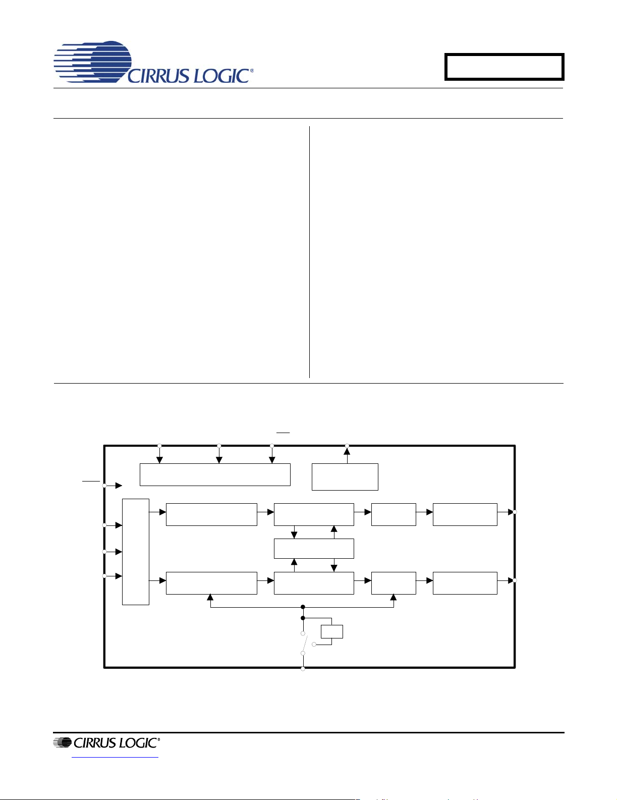
RST
SCLK
LRCK
SDATA
SCL/CCLK MUTECAD0/CS
Serial Port
SDA/CDIN
Control Port
Volume ControlInterpolation Fi lter Analog Filter
Volume ControlInterpolation Fi lter
Mixer
MCLK
External
Mute Control
÷2
∆Σ
∆Σ
DAC
DAC
Analog Filter
AOUTA
AOUTB
http://www.cirrus.com
Copyright © Cirrus Logic, Inc. 2005
(All Rights Reserved)
DECEMBER '05
DS298F5
1
Page 2

TABLE OF CONTENTS
1. CHARACTERISTICS AND SPECIFICATIONS ..................................................................................... 4
SPECIFIED OPERATING CONDITIONS.............................................................................................. 4
ABSOLUTE MAXIMUM RATINGS ........................................................................................................4
ANALOG CHARACTERISTICS (CS4341-KS/CZZ)............................................................................... 5
COMBINED INTERPOLATION & ON-CHIP ANALOG FILTER RESPONSE........................................ 7
SWITCHING SPECIFICATIONS - SERIAL AUDIO INTERFACE........................................................ 10
SWITCHING CHARACTERISTICS - INTERNAL SERIAL CLOCK ..................................................... 11
SWITCHING CHARACTERISTICS - CONTROL PORT INTERFACE (I²C®) ..................................... 12
SWITCHING CHARACTERISTICS - CONTROL PORT INTERFACE (SPI™) ................................... 13
DC ELECTRICAL CHARACTERISTICS.............. ... ... .... ... ... ... .... ... ... .......................................... ... ... ... 14
DIGITAL INPUT CHARACTERISTICS ................................................................................................ 14
DIGITAL INTERFACE SPECIFICATIONS........................................................................................... 14
2. PIN DESCRIPTION ............................................................................................................................. 15
3. TYPICAL CONNECTION DIAGRAM ................................................................................................. 16
4. APPLICATIONS ................................................................................................................................... 17
4.1 Sample Rate Range/Operational Mode ........................................................................................ 17
4.2 System Clocking .................... .... ... ... ... ... .... ...................................... .... ... ... ... .... ... ......................... 17
4.2.1 Internal Serial Clock Mode ...............................................................................................17
4.2.2 External Serial Clock Mode .............................................................................................. 18
4.3 Digital Interface Format ................................................................................................................. 18
4.4 De-Emphasis .......................................................... ...................................................................... 19
4.5 Power-Up Sequence .......... ... .... ... .......................................... ... ................................................... 19
4.6 Popguard
4.6.1 Power-Up ............................................... .... ... ... ... ....................................... ... ... .... ............ 19
4.6.2 Power-Down .................. ... ....................................... ... ... ... ... .... ... ... ................................... 20
4.6.3 Discharge Time ............................................. ... ... .... ...................................... ... .... ... ......... 20
4.7 Mute Control ....................................................... .... ... ... ... .... ... ... ................................................... 20
4.8 Grounding and Power Supply Arrangements ............................................................................... 20
4.9 Control Port Interface .................................................................................................................... 20
4.9.1 Rise Time for Control Port Clock ...................................................................................... 21
4.9.2 Memory Address Pointer (MAP) ...................................................................................... 21
4.9.3 I²C Mode .......................................... ... ... .... ... ....................................... ... ... ... ... .... ............ 21
4.9.4 SPI Mode ............................................ ... .... ... ... ... .... ...................................... ... .... ............ 23
5. REGISTER QUICK REFERENCE ....................................................................................................... 24
6. REGISTER DESCRIPTION ................................................................................................................. 25
6.1 MCLK Control (address 00h)...................... ... ... ............................................................................. 25
6.2 Mode Control (address 01h)............................. ... .... ... ... ... .... ... ... ... ... .... ... ... ... .... ... ......................... 25
6.3 Transition and Mixing Control (address 02h).................................................................................27
6.4 Channel A Volume Control (address 03h)..................................................................................... 29
6.5 Channel B Volume Control (address 04h)..................................................................................... 29
®
Transient Control .............................. .... ... ... ... .... ... ... ... ... .... ... ... ... ................................ 19
4.9.2a INCR (Auto Map Increment) .............................................................................. 21
4.9.2b MAP0-3 (Memory Address Pointer) .................................................................. 21
4.9.3a I²C Write ............................................................................................................ 22
4.9.3b I²C Read ............................................................................................................ 22
4.9.4a SPI Write ........................................................................................................... 23
CS4341
7. PARAMETER DEFINITIONS ............................................................................................................... 31
8. PACKAGE DIMENSIONS .................................................................................................................... 32
2 DS298F5
Page 3

8.1 SOIC ................... ... ... ....................................... ... .... ... ... ....................................... ..........................32
8.2 TSSOP ................................................................... ... ... ... .... ..........................................................33
9. PACKAGE THERMAL RESISTANCE .................................................................................................33
10. REFERENCES ................................ ... ... ... ... .... ... ... ... .... .......................................................................34
11. REVISION HISTORY ..........................................................................................................................34
LIST OF FIGURES
Figure 1. Output Test Load .........................................................................................................................6
Figure 2. Maximum Loading ........................................................................................................................6
Figure 3. Single-Speed Stopband Rejection ...............................................................................................8
Figure 4. Single-Speed Transition Band .....................................................................................................8
Figure 5. Single-Speed Transition Band (Detail) .........................................................................................8
Figure 6. Single-Speed Passband Ripple ...................................................................................................8
Figure 7. Double-Speed Stopband Rejection ..............................................................................................8
Figure 8. Double-Speed Transition Band ....................................................................................................8
Figure 9. Double-Speed Transition Band (Detail) .......................................................................................9
Figure 10. Double-Speed Passband Ripple ..................................................................................................9
Figure 11. Serial Input Timing (External SCLK) ............................................ .... ..........................................10
Figure 12. Internal Serial Mode Input Timing .................................................... ... ... ....................................11
Figure 13. Internal Serial Clock Generation ................................................................................................11
Figure 14. Control Port Timing - I²C Mode ..................................................................................................12
Figure 15. Control Port Timing - SPI Mode .................................................................................................13
Figure 16. Typical Connection Diagram .................................. ................................... .................................16
Figure 17. CS4341 Formats 0-1 - I²S up to 24-Bit Data ..............................................................................18
Figure 18. CS4341 Format 2 - Left Justified up to 24-Bit Data ...................................................................18
Figure 19. CS4341 Formats 3-6 - Right Justified ........................................................................................18
Figure 20. De-Emphasis Curve ...................................................................................................................19
Figure 21. I²C Buffer Example .....................................................................................................................21
Figure 22. I²C Write .....................................................................................................................................22
Figure 23. I²C Read .....................................................................................................................................23
Figure 24. Control Port Timing, SPI Mode ..................................................................................................23
Figure 25. ATAPI Block Diagram ................................................................................................................29
CS4341
LIST OF TABLES
Table 1. CS4341 Speed Modes.....................................................................................................................17
Table 2. Single-Speed Mode Standard Frequencies ................................. ... .......................................... .......17
Table 3. Double-Speed Mode Standard Frequencies....................................................................................17
Table 4. Internal SCLK/LRCK Ratio...............................................................................................................18
Table 5. Digital Interface Format....................................................................................................................26
Table 6. ATAPI Decode.......................... .... ... ... ... ... .... ....................................................................................28
Table 7. Example Digital Volume Settings .....................................................................................................30
DS298F5 3
Page 4
CS4341
1. CHARACTERISTICS AND SPECIFICATIONS
(Min/Max performance characteristics and specifications are guaranteed over the Specified Operating Conditions.
Typical performance characteristics are derived from measurements taken at T
SPECIFIED OPERATING CONDITIONS (All voltages with respect to AGND = 0 V.)
Parameters Symbol Min Nom Max Units
DC Power Supply
Nominal 3.3 V
Nominal 5.0 V
Specified Operating Temperature -KS/CZZ
VA
VA
T
A
(Power Applied)
ABSOLUTE MAXIMUM RATINGS (AGND = 0 V; all voltages with respect to AGND. Operation beyond
these limits may result in permanent damage to the device. Normal opera tion is not guaranteed at these extremes.)
Parameters Symbol Min Max Units
DC Power Supply VA -0.3 6.0 V
Input Current
Digital Input Voltage V
Ambient Operating Temperature (power applied) T
Storage Temperature T
(Note 1) I
in
IND
A
stg
= 25°C.)
A
2.7
4.75
3.3
5.0
3.6
5.5
-10 - +70 °C
-±10mA
-0.3 VA+0.4 V
-55 125 °C
-65 150 °C
V
V
Notes: 1. Any pin except supplies.
4 DS298F5
Page 5
CS4341
ANALOG CHARACTERISTICS (CS4341-KS/CZZ) (Test conditions (unless otherwise specified): Input
test signal is a 997 Hz sine wave at 0 dBFS; measurement bandwidth is 10 Hz to 20 kHz; test load R
= 10 pF (see Figure 1).)
VA = 5.0 V VA = 3.0 V
Parameter
Min Typ Max Min Typ Max Unit
Single-Speed Mode Fs = 48 kHz
Dynamic Range
18 to 24-Bit unweighted
16-Bit unweighted
Total Harmonic Distortion + Noise
18 to 24-Bit 0 dB
16-Bit 0 dB
(Note 2)
A-Weighted
A-Weighted
(Note 2)
-20 dB
-60 dB
-20 dB
-60 dB
93
96
89
98
101
-
-
-
-
-
-
-
-
92
95
-91
-78
-38
-90
-72
-32
-
-
-
-
-86
-
-
-
-
-
92
-
-
-
-
-
-
-
-
94
97
92
95
-94
-74
-34
-91
-72
-32
Double-Speed Mode Fs = 96 kHz
Dynamic Range
18 to 24-Bit unweighted
16-Bit unweighted
Total Harmonic Distortion + Noise
18 to 24-Bit 0 dB
16-Bit 0 dB
(Note 2)
A-Weighted
A-Weighted
(Note 2)
-20 dB
-60 dB
-20 dB
-60 dB
93
96
89
98
101
-
-
-
-
-
-
-
-
92
95
-91
-78
-38
-90
-72
-32
-
-
-
-
-86
-
-
-
-
-
92
-
-
-
-
-
-
-
-
94
97
92
95
-94
-74
-34
-91
-72
-32
=10kΩ, CL
L
-
-
-
-
-89
-
-
-
-
-
-
-
-
-
-89
-
-
-
-
-
dB
dB
dB
dB
dB
dB
dB
dB
dB
dB
dB
dB
dB
dB
dB
dB
dB
dB
dB
dB
DS298F5 5
Page 6
CS4341
ANALOG CHARACTERISTICS (CS4341-KS/CZZ) (Continued)
Parameters Symbol Min Typ Max Units
Dynamic Performance for All Modes
Interchannel Isolation (1 kHz) - 100 - dB
DC Accuracy
Interchannel Gain Mismatch - 0.1 - dB
Gain Drift - ±100 - ppm/°C
Analog Output Characteristics and Specifications
Full-Scale Output Voltage 0.6•VA 0.7•VA 0.8•VA Vpp
Output Impedance - 100 - Ω
Minimum AC-Load Resistance
Maximum Load Capacitance
Notes: 2. One-half LSB of triangular PDF dither is added to data.
3. Refer to Figure 2.
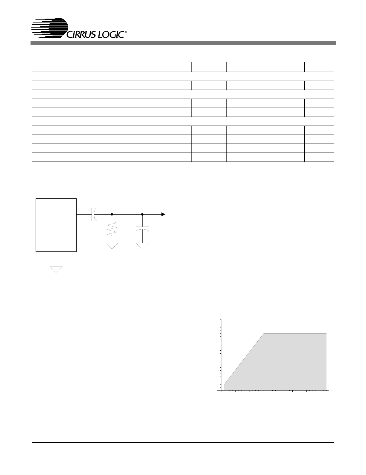
.
3.3 µF
AOUTx
+
(Note 3) R
(Note 3) C
V
out
L
L
-3-kΩ
- 100 - pF
AGND
R
L
Figure 1. Output Test Load
C
L
125
100
L
75
50
25
Capacitive Load -- C (pF)
2.5
51015
3
Safe Operating
Region
Resistive Load -- R (kΩ)
L
20
Figure 2. Maximum Loading
6 DS298F5
Page 7
CS4341
COMBINED INTERPOLATION & ON-CHIP ANALOG FILTER RESPONSE (The filter characteris-
tics and the X-axis of the response plots have been normalized to the sample rate (Fs) and can be referenced to the
desired sample rate by multiplying the given characteristic by Fs.)
Parameter Min Typ Max Unit
Single-Speed Mode - (4 kHz to 50 kHz sample rates)
Passband
to -0.05 dB corner
to -3 dB corner
Frequency Response 10 Hz to 20 kHz -0.02 - +0.08 dB
StopBand 0.5465 - - Fs
StopBand Attenuation
Group Delay - 9/Fs - s
Passband Group Delay Deviation 0 - 20 kHz - ±0.36/Fs - s
De-emphasis Error (Relative to 1 kHz) Fs = 32 kHz
(Note 5) Fs = 44.1 kHz
Fs = 48 kHz
Double-Speed Mode - (50 kHz to 100 kHz sample rates)
Passband
to -0.1 dB corner
to -3 dB corner
Frequency Response 10 Hz to 20 kHz -0.06 - +0.2 dB
StopBand 0.577 - - Fs
StopBand Attenuation
Group Delay - 4/Fs - s
Passband Group Delay Deviation 0 - 40 kHz
0 - 20 kHz
0
0
(Note 4) 50 - - dB
-
-
-
0
0
(Note 4) 55 - - dB
-
-
-
-
-
-
-
-
-
±1.39/Fs
±0.23/Fs
0.4535
0.4998
+0.2/-0.1
+0.05/-0.14
+0/-0.22
0.4621
0.4982
-
-
Fs
Fs
dB
dB
dB
Fs
Fs
s
s
Notes: 4. For Single-Speed Mode, the measurement bandwidth is 0.5465 Fs to 3 Fs.
For Double-Speed Mode, the measurement bandwidth is 0.577 Fs to 1.4 Fs.
5. De-emphasis is only available in Single-Speed Mode.
DS298F5 7
Page 8
CS4341
Figure 3. Single-Speed Stopband Rejection Figure 4. Single-Speed Transition Band
Figure 5. Single-Speed Transition Band (Detail) Figure 6. Single-Speed Passband Ripple
Figure 7. Double-Speed Stopband Rejection Figure 8. Double-Speed Transition Band
8 DS298F5
Page 9
CS4341
Figure 9. Double-Speed Transition Band (Detail) Figure 10. Double-Speed Passband Ripple
DS298F5 9
Page 10
CS4341
SWITCHING SPECIFICATIONS - SERIAL AUDIO INTERFACE
Parameters Symbol Min Max Units
MCLK Frequency 1.024 51.2 MHz
MCLK Duty Cycle 45 55 %
Input Sample Rate Single-Speed Mode
Double-Speed ModeFsFs
4
50
50
100
kHz
kHz
LRCK Duty Cycle 40 60 %
SCLK Pulse Width Low t
SCLK Pulse Width High t
SCLK Frequency Single-Speed Mode
Double-Speed Mode
SCLK rising to LRCK edge delay t
SCLK rising to LRCK edge setup time t
SDIN valid to SCLK rising setup time t
SCLK rising to SDIN hold time t
LRCK
t
t
slrd
slrs
t
sclkl
sclkl
sclkh
slrd
slrs
sdlrs
sdh
t
sclkh
20 - ns
20 - ns
-
-
128xFs
64xFs
Hz
Hz
20 - ns
20 - ns
20 - ns
20 - ns
SCLK
t
sdh
SDATA
t
sdlrs
Figure 11. Serial Input Timing (External SCLK)
10 DS298F5
Page 11
CS4341
SWITCHING CHARACTERISTICS - INTERNAL SERIAL CLOCK
Parameters Symbol Min Typ Max Units
MCLK Frequency 1.024 - 51.2 MHz
MCLK Duty Cycle 45 - 55 %
Input Sample Rate Single-Speed Mode
Double-Speed ModeFsFs
LRCK Duty Cycle
SCLK Period
(Note 7) t
sclkw
SCLK rising to LRCK edge
t
sclkr
SDATA valid to SCLK rising setup time t
SCLK rising to SDATA hold time
sdlrs
t
sdh
MCLK / LRCK = 512, 256 or 128
SCLK rising to SDATA hold time
t
sdh
MCLK / LRCK = 384 or 192
Notes: 6. The Duty Cycle must be 50% +/− 1/2 MCLK Period.
7. See section 4.2.1 for derived internal frequencies.
LRCK
t
sclkr
SDATA
4
50
1
---------------SCLK
--s
1
--------------------- -10+
512()Fs
1
--------------------- -15+
512()Fs
1
--------------------- -15+
384()Fs
-
-
(Note 6)
50
100
kHz
kHz
%
--s
t
sclkw
------------- 2
--ns
--ns
--ns
t
sclkw
t
sdlrstsdh
*INTERNAL SCLK
Figure 12. Internal Serial Mode Input Timing
*The SCLK pulses shown are internal to the CS4341.
LRCK
MCLK
*INTERNAL SCLK
SDATA
1
N
2
N
Figure 13. Internal Serial Clock Generation
* The SCLK pulses shown are internal to the CS4341. N equals MCLK divided by SCLK
DS298F5 11
Page 12

SWITCHING CHARACTERISTICS - CONTROL PORT INTERFACE (I²C®)
Parameter Symbol Min Max Unit
I²C Mode
SCL Clock Frequency f
RST
Rising Edge to Start
Bus Free Time Between Transmissions t
Start Condition Hold Time (prior to first clock pulse) t
Clock Low time t
Clock High Time t
Setup Time for Repeated Start Condition t
SDA Hold Time from SCL Falling
(Note 8) t
SDA Setup time to SCL Rising t
Rise Time of SCL
(Note 9) t
Fall Time of SCL t
Rise Time SDA t
Fall Time of SDA t
Setup Time for Stop Condition t
scl
t
irs
buf
hdst
low
high
sust
hdd
sud
rc
fc
rd
fd
susp
- 100 kHz
500 - ns
4.7 - µs
4.0 - µs
4.7 - µs
4.0 - µs
4.7 - µs
0-µs
250 - ns
-25ns
-25ns
-1µs
-300ns
4.7 - µs
CS4341
Notes: 8. Data must be held for sufficient time to bridge the transition time, tfc, of SCL.
9. See “Rise Time for Control Port Clock” on page 21 for a recommended circuit to meet rise time
specification.
RST
t
SDA
SCL
irs
Stop Start
t
buf
t
hdd
t
high
t
sud
t
hdst
t
low
Figure 14. Control Port Timing - I²C Mode
Repeated
Start
t
sust
t
hdst
t
f
t
r
Stop
t
susp
12 DS298F5
Page 13
SWITCHING CHARACTERISTICS - CONTROL PORT INTERFACE (SPI™)
Parameter Symbol Min Max Unit
SPI Mode
CCLK Clock Frequency f
Rising Edge to CS Falling
RST
CCLK Edge to CS
CS
High Time Between Transmissions
CS
Falling to CCLK Edge
Falling (Note 10)
CCLK Low Time t
CCLK High Time t
CDIN to CCLK Rising Setup Time t
CCLK Rising to DATA Hold Time
Rise Time of CCLK and CDIN
Fall Time of CCLK and CDIN
(Note 11) t
(Note 12) t
(Note 12) t
sclk
t
srs
t
spi
t
csh
t
css
scl
sch
dsu
dh
r2
f2
-6MHz
500 - ns
500 - ns
1.0 - µs
20 - ns
1
----------------MCLK
1
----------------MCLK
40 - ns
15 - ns
-100ns
-100ns
CS4341
-ns
-ns
Notes: 10. t
11. Data must be held for sufficient time to bridge the transition time of CCLK.
12. For f
only needed before first falling edge of CS after RST rising edge. t
spi
< 1 MHz.
sclk
RST
CS
CCLK
CDIN
t
srs
t
t
css
spi
t
r2
Figure 15. Control Port Timing - SPI Mode
t
t
scl
sch
t
f2
t
t
dsu
dh
= 0 at all other times.
spi
t
csh
DS298F5 13
Page 14

CS4341
DC ELECTRICAL CHARACTERISTICS (AGND = 0 V; all voltages with respect to AGND.)
Parameters Symbol Min Typ Max Units
Normal Operation
Power Supply Current VA = 5.0 V
Power Dissipation VA = 5.0 V
Power-down Mode
Power Supply Current VA = 5.0 V
VA = 3.0 V
Power Dissipation VA = 5.0 V
All Modes of Operation
Power Supply Rejection Ratio
V
Nominal Voltage
Q
Output Impedance
Maximum allowable DC current source/sink
Filt+ Nominal Voltage
Output Impedance
Maximum allowable DC current source/sink
MUTEC Low-Level Output Voltage - 0 - V
MUTEC High-Level Output Voltage - VA - V
Maximum MUTEC Drive Current - 3 - mA
(Note 13)
(Note 14)
VA = 3.0 V
VA = 3.0 V
VA = 3.0 V
(Note 15) 1 kHz
60 Hz
I
A
I
A
I
A
PSRR -
-
-
-
-
-
-
-
-
-
-
-
-
-
-
-
15
11
75
33
60
30
0.3
0.09
60
40
0.45•VA
250
0.01
VA
250
0.01
18
14
90
42
mA
mA
mW
mW
-
-
-
-
-
-
µA
µA
mW
mW
dB
dB
-
-
-
kΩ
mA
-
-
-
kΩ
mA
V
V
Notes: 13. Normal operation is defined as RST
= HI with a 997 Hz, 0 dBFS input sampled at the highest Fs for
each speed mode, and open outputs, unless otherwise specified.
14. Power Down Mode is defined as RST
= LO with all clocks and data lines held static.
15. Valid with the recommended capacitor values on FILT+ and VQ as shown in Fig ure 16. Incr easing the
capacitance will also increase the PSRR.
DIGITAL INPUT CHARACTERISTICS (AGND = 0 V; all voltages with respect to AGND.)
Parameters Symbol Min Typ Max Units
Input Leakage Current I
in
--±10µA
Input Capacitance - 8 - pF
DIGITAL INTERFACE SPECIFICATIONS (AGND = 0 V; all voltages with respect to AGND.)
Parameters Symbol Min Max Units
3.3 V Logic (3.0 V to 3.6 V DC Supply)
High-Level Input Voltage V
Low-Level Input Voltage V
5.0 V Logic (4.75 V to 5.25 V DC Supply)
High-Level Input Voltage V
Low-Level Input Voltage V
IH
IL
IH
IL
2.0
-0.8V
2.0 - V
-0.8V
-
V
14 DS298F5
Page 15

2. PIN DESCRIPTION
CS4341
SDATA AOUTA
SCLK VA
LRCK AGND
MCLK AOUTB
SCL/CCLK REF_GND
SDA/CDIN VQ
AD0/CS
Pin Name # Pin Description
RST
SDATA
SCLK
LRCK
MCLK
SCL/CCLK
SDA/CDIN
AD0/CS
FILT+
VQ
REF_GND
AOUTB
AOUTA
AGND
VA
MUTEC
Reset (Input) - Powers down device and resets registers to their default settings.
1
Serial Audio Data (Input) - Input for two’s complement serial audio data.
2
Serial Clock (Input) -Serial clock for the serial audio interface.
3
Left Right Clock (Input) - Determines which channel, Left or Right, is currently active on the
4
serial audio data line.
Master Clock (Input) - Clock source for the delta-sigma modulator and digital filters.
5
Serial Control Port Clock (Input) - Serial clock for the control port interface.
6
7 Serial Control Data I/O (Input/Output) - Input/Output for I²C data. Input for SPI data.
Address Bit / Chip Select (Input) - Chip address bit in I²C Mode. Control signal used to select
8
the chip in SPI mode.
Positive Voltage Reference (Output) - Positive voltage reference for the internal
9
sampling circuits.
Quiescent Voltage (Output) - Filter connection for internal quiescent reference voltage.
10
Reference Ground (Input) - Ground reference for the internal sampling circuits.
11
Analog Outputs (Output) - The full-scale analog output level is specified in the
12
Analog Characteristics table.
15
Analog Ground (Input)
13
14 Power (Input) - Positive power for the analog, digital, and serial audio interface sections.
Mute Control (Output) - Control signal for an optional mute circuit.
16
RST MUTEC
161
152
143
134
125
116
107
98
FILT+
DS298F5 15
Page 16

3. TYPICAL CONNECTION DIAGRAM
CS4341
Serial Audio
Data
Processor
External Clock
Mic r o-Controlled
Configuration
2
3
4
5
6
7
8
1
SDATA
SCLK
LRCK
MCLK
SCL/CC LK
SDA/CDIN
AD0/CS
RST
AGND
14
VA
CS4341
13
0.1 µF
AOUTA
MUTEC
FILT+
VQ
REF_GND
AOUT B
12
15
16
9
10
11
3.3 µF
+
10 k
.1 µ F
3.3 µF
+
10 k
1µF
560
560
+3.0 V or + 5 .0 V
Ω
C
+
0.1 µF
1µF
Ω
C
C=
OPTIONAL
MUTE
CIRCUIT
R560
+
L
π
4
Fs(R
L
560)
Audio
Output A
R
L
Audio
Output B
R
L
+
Ω
1µF
+
Ω
Figure 16. Typical Connection Diagram
16 DS298F5
Page 17

CS4341
4. APPLICATIONS
4.1 Sample Rate Range/Operational Mode
The device operates in one of two operational modes determined by the Master Clock to Left/Right Clock
ratio (see section 4.2). Sample rates outside the specified range for each mode are not supported.
Input Sample Rate (Fs) MODE
4 kHz - 50 kHz Single-Speed Mode
50 kHz - 100 kHz Double-Speed Mode
Table 1. CS4341 Speed Modes
4.2 System Clocking
The device requires external generation of the master (MCLK) and left/right (LRCK) clocks. The device
also requires external generation of the serial clock (SCLK) if the internal serial clock is not used. The
LRCK, defined also as the input sample rate Fs, must be synchronously derived from MCLK according to
specified ratios. The specified ratios of MCLK to LRCK, along with several standard audio sample rates
and the required MCLK frequency, are illustrated in Tables 2 and 3.
Sample Rate
(kHz)
32 8.1920 12.2880 16.3840 24.5760 32.768
44.1 11.2896 16.9344 22.5792 33.8688 45.1584
48 12.2880 18.4320 24.5760 36.8640 49.1520
Sample Rate
(kHz)
64 8.1920 12.2880 16.3840 24.5760
88.2 11.2896 16.9344 22.5792 33.8688
96 12.2880 18.4320 24.5760 36.8640
256x 384x 512x 768x* 1024x*
Table 2. Single-Speed Mode Standard Frequencies
128x 192x 256x* 384x*
Table 3. Double-Speed Mode Standard Frequencies
MCLK (MHz)
MCLK (MHz)
*Requires MCLKDIV bit = 1 in the MCLK Control (address 00h) register.
4.2.1 Internal Serial Clock Mode
The device will enter the Internal Serial Clock Mode if no low to high transitions are detected on
the SCLK pin for 2 consecutive periods of LRCK. In this mode, the SCLK is internally derived and
synchronous with MCLK and LRCK. The SCLK/LRCK ratio is either 32, 48, or 64 depending upo n
the MCLK/LRCK ratio and the Digital Interface Format selection (see Table 4).
Operation in the Internal Serial Clock mode is identical to operation with an external SCLK synchronized with LRCK; however, External SCLK mode is recommended for system clocking applications.
DS298F5 17
Page 18

CS4341
Input
MCLK/LRCK
Ratio
512, 256, 128
384, 192
512, 256, 128
I2S up to 16 or
24 Bits
(Format 1) - - X 32
XX X X48
(Format 0) X X - 64
Digital Interface Format Selection Internal
Left Justified 24
Bits
Right Justified
18, 20 or 24 Bits
Right Justified
16 Bits
SCLK/LRCK
Ratio
Table 4. Internal SCLK/LRCK Ratio
4.2.2 External Serial Clock Mode
The device will enter the External Serial Clock Mode whenever 16 low to high transitions are detected on the SCLK pin during any phase of the LRCK period. The device will revert to Internal
Serial Clock Mode if no low to high transitions are detected on the SCLK pin for 2 consecutive periods of LRCK.
4.3 Digital Interface Format
The device will accept audio samples in several digital interface formats. The desired format is selected
via the DIF0, DIF1 and DIF2 bits in the Mode Control register (see section 6.2.2). For an illustration of the
required relationship between LRCK, SCLK and SDATA, see Figures 17 through 19.
LRCK
SCLK
Left Channel
Right Channel
SDATA +3 +2 +1+5 +4
MSB
-1 -2 -3 -4 -5
Figure 17. CS4341 Formats 0-1 - I²S up to 24-Bit Data
LRCK
SCLK
SDATA +3 +2 +1+5 +4
MSB
-1 -2 -3 -4 -5
Left Channel
Figure 18. CS4341 Format 2 - Left Justified up to 24-Bit Data
LRCK
SCLK
SDATA
LSB
Left Channel
-1 -2 -3 -4
MSB LSB
-5
Figure 19. CS4341 Formats 3-6 - Right Justified
LSB
LSB
+6 +5 +4 +3 +2 +1+7
MSB LSB
-1 -2 -3 -4
MSB
-1 -2 -3 -4
Right Channel
-1 -2 -3 -4
MSB LSB
+3 +2 +1+5 +4
Right Channel
-5
+3 +2 +1+5 +4
LSB
+6 +5 +4 +3 +2 +1+7
18 DS298F5
Page 19

CS4341
4.4 De-Emphasis
The device includes on-chip digital de-emphasis. The Mode Control (address 01h) bits select either the
32, 44.1 or 48 kHz de-emphasis filter. Figure 20 shows the de-emphasis curve for F
The frequency response of the de-emphasis curve will scale proportionally with changes in sample
rate, Fs. Please see section 6.2.3 for the desired de-emphasis control.
De-emphasis is only available in Single-Speed Mode.
Gain
dB
T1=50 µs
0dB
equal to 44.1 kHz.
s
-10dB
F1 F2
3.183 kHz 10.61 kHz
Figure 20. De-Emphasis Curve
T2 = 15 µs
Frequency
4.5 Power-Up Sequence
1) Hold RST low until the power supply is stable, and the master and left/right clocks are locked to the
appropriate frequencies, as discussed in section 4.2. In this state, the control port is reset to its default
settings and VQ will remain low.
2) Bring RST
high. The device will remain in a low power state with VQ low.
3) Load the desired register settings while keeping the PDN bit set to 1.
4) Set the PDN bit to 0. This will initiate the power-up sequence, which lasts approximately 50 µS when
the POR bit is set to 0. If the POR bit is set to 1, see section 4.6 for a complete description of powerup timing.
4.6 Popguard® Transient Control
The CS4341 uses Popguard® technology to minimize the effects of output transients during power-up and
power-down. This technology, when used with external DC-blocking capacitors in series with the audio
outputs, minimizes the audio transients commonly produced by single-ended single-supply converters. It
is activated inside the DAC when RST
from choosing the appropriate DC-blocking capacitors.
is enabled/disabled and requires no other external control, aside
4.6.1 Power-Up
When the device is initially powered-up, the audio outputs, AOUTL and AOUTR, are clamped to
AGND. Following a delay of approximately 1000 sample periods, each output begins to ramp toward the quiescent voltage. Approximately 10,000 LRCK cycles later, the outputs reach V
audio output begins. This gradual voltage ramping allows time for the external DC-blocking capacitors to charge to the quiescent voltage, minimizing the power-up transient.
DS298F5 19
and
Q
Page 20

CS4341
4.6.2 Power-Down
To prevent transients at power-down, the device must first enter its power-down state by enabling
or setting the PDN bit. When this occurs, audio output ceases and the in ternal output buffers
RST
are disconnected from AOUTL and AOUTR. In their place, a soft-start current sink is substituted
which allows the DC-blocking capacitors to slowly discharge. Once this charge is dissipated, the
power to the device may be turned off and the system is ready for the next power-on.
4.6.3 Discharge Time
To prevent an audio transient at the next power-on, it is necessary t o ensure that the DC-blockin g
capacitors have fully discharged before turning on the power or exiting the power-down state. If
not, a transient will occur when the audio outputs are initially clamped to AGND. The time that the
device must remain in the power-down state is related to the value of the DC-blocking capacitance.
For example, with a 3.3 µF capacitor, the minimum power-down time will be approximately
0.4 seconds.
4.7 Mute Control
The Mute Control pin goes high during power-up initialization, reset, muting (see section 6.2.1 a nd 6.5.1)
or if the MCLK to LRCK ratio is incorrect. This pin is intended to be used as a control for an external mute
circuit to prevent the clicks and pops that can occur in any single-ended single supply system.
Use of the Mute Control function is not mandatory but recommended for designs requiring the absolute
minimum in extraneous clicks and pops. Also, use of the Mute Control function can enable the system
designer to achieve idle channel noise/signal-to-noise ratios which are only limited by the external mute
circuit. See the CDB4341 data sheet for a suggested mute circuit.
4.8 Grounding and Power Supply Arrangements
As with any high resolution converter, the CS4341 requires careful attention to power supply and grounding arrangements if its potential performance is to be realized. Figure 16 shows t he recommended power
arrangements, with VA connected to a clean supply. If the ground planes are split betwee n digital ground
and analog ground, REF_GND & AGND should be connected to the analog ground plane.
Decoupling capacitors should be as close to the DAC as possible, with the low value ceramic capacitor
being the closest. To further minimize impedance, these capacitors should be located on the same layer
as the DAC.
All signals, especially clocks, should be kept away from the FILT+ and VQ pins in order to avoid unwanted
coupling into the modulators. The FILT+ and VQ decoupling capacitors, particularly the 0.1 µF, must be
positioned to minimize the electrical path from FILT+ and REF_GND (as well as VQ and REF_GND), and
should also be located on the same layer as the DAC. The CDB4341 evaluation board demonstrates t he
optimum layout and power supply arrangements.
4.9 Control Port Interface
The control port is used to load all the internal register settings (see section 6). The operation o f the control
port may be completely asynchronous with the audio sample rate. However, to avoid potential interference problems, the control port pins should remain static if no operation is required.
The control port operates in one of two modes: I²C or SPI.
Notes: MCLK must be applied during all I²C communication.
20 DS298F5
Page 21

4.9.1 Rise Time for Control Port Clock
When excess capacitive loading is present on the I²C clock line, pin 6 (SCL/CCLK) may not have
sufficient hysteresis to meet the standard I²C rise time specification. This prevents the use of common I²C configurations with a resistor pull-up. A workaround is achieved by placing a Schmitt Trigger buffer, a 74HC14 for example, on the SCL line just prior to the CS4341. This will not affect the
operation of the I²C bus as pin 6 is an input only.
VA
CS4341
SCL
Figure 21. I²C Buffer Example
Pin 6
4.9.2 Memory Address Pointer (MAP)
The MAP byte precedes the control port register byte during a write operation and is not available
again until after a start condition is initiated. During a read operation the byte transmitted after the
will contain the data of the register pointed to by the MAP (see section 4.9.3 for write/read
ACK
details).
76543210
INCR Reserved Reserved Reserved MAP3 MAP2 MAP1 MAP0
00000000
4.9.2a INCR (Auto Map Increment)
The device has a MAP auto increment capability enabled by the INCR bit (the MSB) of the MAP.
If INCR is set to 0, MAP will stay constant for successive I²C writes or reads and SPI writes. If INCR
is set to 1, MAP will auto increment after each byte is written, allowing block reads or writes of successive registers.
Default = ‘0’
0 - Disabled
1 - Enabled
4.9.2b MAP0-3 (Memory Address Pointer)
Default = ‘0000’
4.9.3 I²C Mode
In the I²C Mode, data is clocked into and out of the bi-directional serial control data line, SDA, by
the serial control port clock, SCL. There is no CS
address (001000[AD0][R/W
the device. If the device ever detects a high to low transition on the AD0/CS
SPI mode will be selected.
DS298F5 21
]) and should be tied to VA or AGND as required, before powering up
pin. Pin AD0 enables the user to alter the chip
pin after power-up,
Page 22

CS4341
4.9.3a I²C Write
To write to the device, follow the procedure below while adhering to the control port Switching
Specifications in section 6.
1) Initiate a START condition to the I²C bus followed by the address byte. The upper 6 bits must
be 001000. The seventh bit must match the setting of the AD0 pin, and the eighth must be 0.
The eighth bit of the address byte is the R/W
2) Wait for an acknowledge (ACK) from the part, then write to the memory address pointer, MAP.
This byte points to the register to be written.
3) Wait for an acknowledge (ACK) from the part, then write the desired data to the register pointed to by the MAP.
4) If the INCR bit (see section 4.9.2a) is set to 1, repeat the previous step until all the desired
registers are written, then initiate a STOP condition to the bus.
5) If the INCR bit is set to 0 and further I²C writes to other registers are desired, it is necessary to
repeat the procedure detailed from step 1. If no further writes to other registers are desired,
initiate a STOP condition to the bus.
SDA
SCL
Start
001000 AD0
W
Figure 22. I²C Write
1-8
MAP
ACK
bit.
ACK
DATA
1-8
ACK
Stop
4.9.3b I²C Read
To read from the device, follow the procedure below while adhering to the control port Switching
Specifications. During this operation it is first necessary to write to the device, specifying the appropriate register through the MAP.
1) After writing to the MAP (see section 4.9.3a), initiate a repeated START condition to the I²C
bus followed by the address byte. The upper 6 bits must be 001000. The seventh bit must
match the setting of the AD0 pin, and the eighth must be 1. The eighth bit of the address byte
is the R/W
2) Signal the end of the address byte by not issuing an acknowledge. The device will then transmit the contents of the register pointed to by the MAP. The MAP will contain the address of the
last register written to the MAP.
3) If the INCR bit is set to 1, the device will continue to transmit the contents of successive registers. Continue providing a clock but do not issue an ACK on the bytes clocked out of the device. After all the desired registers are read, initiate a STOP condition to the bus.
4) If the INCR bit is set to 0 and further I²C reads from other registers are desired, it is necessary
to repeat the procedure detailed from step 1. If no further reads from other registers are desired, initiate a STOP condition to the bus.
bit.
22 DS298F5
Page 23

CS4341
SDA
SCL
001000 AD 0 W
Start
4.9.4 SPI Mode
In SPI mode, data is clocked into the serial control data line, CDIN, by the serial control port clock,
CCLK (see Figure 24 for the clock to data relationship). There is no AD0 pin. Pin CS
select signal and is used to control SPI writes to the control port. When the device detects a high
to low transition on the AD0/CS
and data is clocked in on the rising edge of CCLK.
4.9.4a SPI Write
To write to the device, follow the procedure below while adhering to the control port Switching
Specifications in section 1.
1) Bring CS
2) The address byte on the CDIN pin must then be 00100000.
low.
ACK
MAP
1-8
ACK
Repeated START
Aborted WRITE
Figure 23. I²C Read
001000 AD0 R
or
ACK
Data 1-8
(pointed to by MAP)
ACK
Data 1-8
(pointed to by MAP)
Stop
is the chip
pin after power-up, SPI mode will be selected. All signals are inputs
3) Write to the memory address pointer, MAP. This byte points to the register to be written.
4) Write the desired data to the register pointed to by the MAP.
5) If the INCR bit (see section 4.9.2a) is set to 1, repeat the previous step until all the desired
registers are written, then bring CS
high.
6) If the INCR bit is set to 0 and further SPI writes to other registers are desired, it is necessary
to bring CS
registers are desired, bring CS
high, and repeat the procedure detailed from step 1. If no further writes to other
high.
CS
CCLK
CHIP
ADDRESS
CDIN
0010000
MAP = Memory Address Pointer
Figure 24. Control Port Timing, SPI Mode
R/W
MAP
MSB
byte 1
DATA
LSB
byte n
DS298F5 23
Page 24

CS4341
5. REGISTER QUICK REFERENCE
Addr Function 7 6 5 4 3 2 1 0
0h MCLK Control Reserved Rese rved Reserved Reserved Reserved Reserved MCLKDIV Reserved
DEFAULT 00000000
1h Mode Control 2 AMUTE DIF2 DIF1 DIF0 DEM1 DEM1 POR PDN
DEFAULT 10000011
2h Transition and Mixing
Control
DEFAULT 00000000
3h Channel A Volume
Control
DEFAULT 00000000
4h Channel B Volume
Control
DEFAULT 00000000
A = B SCZ1 SCZ0 ATAPI4 ATAPI3 ATAPI2 ATAPI1 ATAPI0
MUTEA VOLA6 VOLA5 VOLA4 VOLA3 VOLA2 VOLA1 VOLA0
MUTEB VOLB6 VOLB5 VOLB4 VOLB3 VOLB2 VOLB1 VOLB0
24 DS298F5
Page 25

CS4341
6. REGISTER DESCRIPTION
NOTE: All registers are read/write in I²C Mode and write only in SPI mode, unless otherwise stated.
6.1 MCLK CONTROL (ADDRESS 00H)
76543210
Reserved Reserved Reserved Reserved Reserved Reserved MCLKDIV Reserved
00000000
6.1.1 MCLK DIVIDE-BY-2 (MCLKDIV) BIT 1
Default = 0
0 - Disabled
1 - Enabled
Function:
The MCLKDIV bit enables a circuit which divides the externally applied MCLK signal by 2.
6.2 MODE CONTROL (ADDRESS 01H)
76543210
AMUTE DIF2 DIF1 DIF0 DEM1 DEM0 POR PDN
10000011
6.2.1 AUTO-MUTE (AMUTE) BIT 7
Default = 1
0 - Disabled
1 - Enabled
Function:
The Digital-to-Analog converter output will mute following the reception of 8192 consecutive audio
samples of static 0 or -1. A single sample of non-zero data will release the mute. Detection and muting
is done independently for each channel. The quiescent voltage on the output will be retained and the
Mute Control pin will go active during the mute period. The muting function is affected, similar to volume control changes, by the Soft and Zero Cross bits in the Transition and Mixing Control (address
02h) register.
DS298F5 25
Page 26
CS4341
6.2.2 DIGITAL INTERFACE FORMAT (DIF) BIT 4-6
Default = 000 - Format 0 (I²S, up to 24-bit data, 64 x Fs Internal SCLK)
Function:
The required relationship between the Left/Right clock, serial clock and serial data is defined by the
Digital Interface Format and the options are detailed in Figures
DIF2 DIF1 DIF0 DESCRIPTION Format FIGURE
0 0 0 I²S, up to 24-bit data, 64Fs Internal SCLK 0 17
0 0 1 I²S, up to 16-bit data, 32Fs Internal SCLK 1 17
0 1 0 Left Justified, up to 24-bit data, 2 18
0 1 1 Right Justified, 24-bit data 3 19
1 0 0 Right Justified, 20-bit data 4 19
1 0 1 Right Justified, 16-bit data 5 19
1 1 0 Right Justified, 18-bit data 6 19
1 1 1 Identical to Format 1 1 17
Table 5. Digital Interface Format
6.2.3 DE-EMPHASIS CONTROL (DEM) BIT 2-3
Default = 00
00 - Disabled
01 - 44.1 kHz
10 - 48 kHz
11 - 32 kHz
17 through 19.
Function:
Implementation of the standard 15µs/50µs digital de-emphasis filter response, Figure 20, requir es reconfiguration of the digital filter to maintain the proper filter response for 32, 44.1 or 48 kHz sample
rates.
NOTE: De-emphasis is only available in Single-Speed Mode.
6.2.4 POPGUARD
®
TRANSIENT CONTROL (POR) BIT 1
Default = 1
0 - Disabled
1 - Enabled
Function:
The Popguard
®
Transient Control allows the quiescent voltage to slowly ramp to and from 0 volts to
the quiescent voltage during power-on or power-down. Please refer to section 4.6 for implementatio n
details.
6.2.5 POWER DOWN (PDN)
Default = 1
0 - Disabled
1 - Enabled
Function:
The device will enter a low-power state when this function is enabled. The power-down bit defaults to
‘enabled’ on power-up and must be disab led befor e normal opera tion can occur. The contents of the
control registers are retained in this mode.
BIT 0
26 DS298F5
Page 27

CS4341
6.3 TRANSITION AND MIXING CONTROL (ADDRESS 02H)
76543210
A = B SZC1 SZC0 ATAPI4 ATAPI3 ATAPI2 ATAPI1 ATAPI0
01001001
6.3.1 CHANNEL A VOLUME = CHANNEL B VOLUME (A = B) BIT 7
Default = 0
0 - Disabled
1 - Enabled
Function:
The AOUTA and AOUTB volume levels are independ ently controlled by the A an d the B Channel Volume Control Bytes when this function is disabled. The volume on both AOUTA and AOUTB are determined by the A Channel Volume Control Byte and the B Channel Byte is ignored when this function
is enabled.
6.3.2 SOFT RAMP AND ZERO CROSS CONTROL (SZCX)
Default = 10
00 - Immediate Changes
01 - Changes On Zero Crossings
10 - Soft Ramped Changes
11 - Soft Ramped Changes On Zero Crossings
Function:
Immediate Changes
When Immediate Changes is selected all level changes will take effect immediately in one step.
Changes On Zero Crossings
Changes on Zero Crossings dictates that signal level changes, either by attenuation changes or mu ting, will occur on a signal zero crossing to minimize audible artifacts. The requested level change will
occur after a timeout period between 512 and 1024 sample periods (10.7 ms to 21.3 ms at 48 kHz
sample rate) if the signal does not encounter a zero crossing. T he zero cross function is independen tly monitored and implemented for each channel.
Soft Ramped Changes
Soft Ramped Changes allows level changes, both muting and attenuation, to be implemented by incrementally ramping, in 1/8 dB steps, from the current level to the new level at a rate of 1dB per 8
left/right clock periods.
BIT 5-6
Soft Ramped Changes on Zero Crossings
Soft Ramped Changes On Zero Crossings dictates that signal level changes, either by attenuation
changes or muting, will occur in 1/8 dB steps implemented on a signal zero crossing. The 1/8 dB level
change will occur after a timeout period between 512 and 1024 sample periods (10.7 ms to 21.3 ms
at 48 kHz sample rate) if the signal does not encounter a zero crossing. The zero cross function is
independently monitored and implemented for each channel.
DS298F5 27
Page 28

6.3.3 ATAPI CHANNEL MIXING AND MUTING (ATAPI) BIT 0-4
Default = 01001 - AOUTA = Left Channel, AOUTB = Right Channel (Stereo)
Function:
The CS4341 implements the channel mixing functions of the ATAPI CD-ROM specification. Refer to
Table 6 and Figure 25 for additional information.
ATAPI4 ATAPI3 ATAPI2 ATAPI1 ATAPI0 AOUTA AOUTB
00000 MUTE MUTE
00001 MUTE bR
00010 MUTE bL
00011 MUTE b[(L+R)/2]
00100 aR MUTE
00101 aR bR
00110 aR bL
00111 aR b[(L+R)/2]
01000 aL MUTE
01001 aL bR
01010 aL bL
01011 aL b[(L+R)/2]
0 1 1 0 0 a[(L+R)/2] MUTE
0 1 1 0 1 a[(L+R)/2] bR
0 1 1 1 0 a[(L+R)/2] bL
0 1 1 1 1 a[(L+R)/2] b[(L+R)/2]
10000 MUTE MUTE
10001 MUTE bR
10010 MUTE bL
10011 MUTE bL/2
10100 aR MUTE
10101 aR bR
10110 aR bL
10111 aR [(aR+bL)/2]
11000 aL MUTE
11001 aL bR
11010 aL bL
1 1 0 1 1 aL [(aL+bR)/2]
11100 aL/2 MUTE
1 1 1 0 1 [(aL+bR)/2] bR
1 1 1 1 0 [(bL+aR)/2] bL
1 1 1 1 1 [(aL+bR)/2] [(aL+bR)/2]
CS4341
Table 6. ATAPI Decode
28 DS298F5
Page 29
CS4341
Left Channel
Audio Data
A Channel
Volume
Control
ΣΣ
Right Channel
Audio Data
Figure 25. ATAPI Block Diagram
6.4 CHANNEL A VOLUME CONTROL (ADDRESS 03H)
Same as CHANNEL B Volume Control.
6.5 CHANNEL B VOLUME CONTROL (ADDRESS 04H)
B Channel
Volume
Control
MUTE
MUTE
AoutA
AoutB
76543210
MUTEx VOLx6 VOLx5 VOLx4 VOLx3 VOLx2 VOLx1 VOLx0
00000000
6.5.1 MUTE (MUTE) BIT 7
Default = 0
0 - Disabled
1 - Enabled
Function:
The Digital-to-Analog converter output will mute when enabled. The quiescent voltage on the output
will be retained. The muting function is affected, similar to attenuation changes, by the Soft and Zero
Cross bits in the Transition and Mixing Control (address 02h) register. The MUTEC will go active during the mute period if the Mute function is enabled for both channels.
DS298F5 29
Page 30
6.5.2 VOLUME (VOLx) BIT 0-6
Default = 0 dB (No Attenuation)
Function:
The digital volume control allows the user to attenuate the signal in 1 dB increments from 0 to -90 dB.
Volume settings are decoded as shown in Table 7. The volume changes are implemented as dictated
by the Soft and Zero Cross bits in the Transition and Mixing Control (address 02 h) register. All volume
settings less than - 94 dB are equivalent to enabling the Mute bit.
Binary Code Decimal Value Volume Setting
CS4341
0000000 0 0 dB
0010100 20 -20 dB
0101000 40 -40 dB
0111100 60 -60 dB
1011010 90 -90 dB
Table 7. Example Digital Volume Settings
30 DS298F5
Page 31

7. PARAMETER DEFINITIONS
Total Harmonic Distortion + Noise (THD+N)
The ratio of the rms value of the signal to the rms sum of all other spectral components over the specified
bandwidth (typically 10 Hz to 20 kHz), including distortion components. Expressed in decibels.
Dynamic Range
The ratio of the full-scale rms value of the signal to the rms sum of all other spe ctral components over the
specified bandwidth. Dynamic range is a signal-to-noise measurement over the specified bandwidth
made with a -60 dBFS signal. 60 dB is then adde d to the resulting measurement to refer the measurement
to full scale. This technique ensures that the distortion components are below the noise level and do not
affect the measurement. This measurement technique has been accepted by the Audio Engineering
Society, AES17-1991, and the Electronic Industries Association of Japan, EIAJ CP-307.
Interchannel Isolation
A measure of crosstalk between the left and right channels. Mea sured for each channel at the converter’s
output with all zeros to the input under test and a full-scale signal applied to the other channel. Units in
decibels.
Interchannel Gain Mismatch
The gain difference between left and right channels. Units in decibels.
CS4341
Gain Error
Gain Drift
The deviation from the nominal full-scale analog output for a full-scale digital input.
The change in gain value with temperature. Units in ppm/°C.
DS298F5 31
Page 32

8. PACKAGE DIMENSIONS
8.1 SOIC
16L SOIC (150 MIL BODY) PACKAGE DRAWING
1
b
CS4341
E
H
c
∝
L
SEATING
PLANE
D
A
e
A1
INCHES MILLIMETERS
DIM MIN NOM MAX MIN NOM MAX
A 0.053 0.064 0.069 1.35 1.63 1.75
A1 0.004 0.006 0.010 0.10 0.15 0.25
b 0.013 0.016 0.020 0.33 0.41 0.51
C 0.0075 0.008 0.010 0.19 0.20 0.25
D 0.386 0.390 0.394 9.80 9.91 10.00
E 0.150 0.154 0.157 3.80 3.90 4.00
e 0.040 0.050 0.060 1.02 1.27 1.52
H 0.228 0.236 0.244 5.80 6.0 6.20
L 0.016 0.025 0.050 0.40 0.64 1.27
∝ 0° 4° 8° 0° 4° 8°
JEDEC #: MS-012
Controling Dimension is Millimeters
32 DS298F5
Page 33

8.2 TSSOP
N
CS4341
16L TSSOP (4.4 mm BODY) PACKAGE DRAWING
1
23
TOP VIEW
D
E
e
2
b
SIDE VIEW
A2
A1
A
SEATING
PLANE
L
INCHES MILLIMETERS
1
E1
END VIEW
NOTE
DIM MIN NOM MAX MIN NOM MAX
A -- -- 0.043 -- -- 1.10
A1 0.002 0.004 0.006 0.05 -- 0.15
A2 0.03346 0.0354 0.037 0.85 0.90 0.95
b 0.00748 0.0096 0.012 0.19 0.245 0.30 2,3
D 0.193 0.1969 0.201 4.90 5.00 5.10 1
E 0.248 0.2519 0.256 6.30 6.40 6.50
E1 0.169 0.1732 0.177 4.30 4.40 4.50 1
e -- 0.026 BSC -- -- 0.65 BSC --
L 0.020 0.024 0.028 0.50 0.60 0.70
∝
0° 4° 8° 0° 4° 8°
∝
JEDEC #: MO-153
Controlling Dimension is Millimeters
Notes: 1. “D” and “E1” are reference datums and do not included mold flash or protrusions, but do include mold
mismatch and are measured at the parting line, mold flash or protrusions shall not exceed 0.20 mm per
side.
2. Dimension “b” does not include dambar protrusion/intrusion. Allowable dambar protrusion shall be
0.13 mm total in excess of “b” dimension at maximum material condition. Dambar intrusion shall not
reduce dimension “b” by more than 0.07 mm at least material condition.
3. These dimensions apply to the flat section of the lead between 0.10 and 0.25 mm from lead tips.
9. PACKAGE THERMAL RESISTANCE
Package Symbol Min Typ Max Units
SOIC
TSSOP (for multi-layer boards)
DS298F5 33
(for multi-layer boards)
θ
JA
θ
JA
-
-
74
89
-
°C/Watt
-
°C/Watt
Page 34

10.REFERENCES
CDB4341 Evaluation Board Datasheet
11.REVISION HISTORY
Revision Changes
F4
F5
Added lead-free packaging information
Corrected Dimension e in TSSOP Package Drawing value for NOM Millimeters from 0.065 to 0.65
CS4341
Contacting Cirrus Logic Support
For all product questions and inquiries, contact a Cirrus Logic Sales Representative.
To find the one nearest to you, go to www.cirrus.com/corporate/contacts/sales.cfm
IMPORTANT NOTICE
Cirrus Logic, Inc. and its subsidiaries ("Cirrus") believe that the information contained in this document is accurate and reliable. However, the information is subject
to change without not ice and is pr ovided "AS IS" witho ut warr anty of any kind (express or implied). Customers are advised to obtain the latest version of relevant
information to verify, before placing orders, that information being relied on is current and complete. All products are sold subject to the terms and conditions of sale
supplied at the time of order acknowledgment, including those pertaining to warranty, indemnification, and limitation of liability. No responsibility is assumed by Cirrus
for the use of this information, including use of this information as the basis for manufacture or sale of any items, or for infringement of patents or other rights of third
parties. This document is the property of Cirrus and by furnishing this information, Cirrus grants no license, express or implied under any patents, mask work rights,
copyrights, trademarks, trade secrets or other intelle ctual property rights. Ci rrus owns the cop yrights associated with the information contained herein and gives consent for copies to be made of the information only for use within your organization with respect to Cirrus integrated circuits or other products of Cirrus. This consent
does not extend to other copying such as copying for general distribution, advertising or promotional purposes, or for creating any work for resale.
CERTAIN APPLICATIONS USING SEMICONDUCTOR PRODUCTS MAY INVOLVE POTENTIAL RISKS OF DEATH, PERSONAL INJURY, OR SEVERE PROPERTY OR ENVIRONMENTAL DAMAGE (“CRITICAL APPLICATIONS”). CIRRUS PRODUCTS ARE NOT DESIGNED, AUTHORIZED OR WARRANTED FOR USE
IN AIRCRAFT SYSTEMS, MILITARY APPLICATIONS, PRODUCTS SURGICALLY IMPLANTED INTO THE BODY, AUTOMOTIVE SAFETY OR SECURITY DEVICES, LIFE SUPPORT PRODUCTS OR OTHER CRITICAL APPLICATIONS. INCLUSION OF CIRRUS PRODUCTS IN SUCH APPLICATIONS IS UNDERSTOOD TO BE FULLY AT THE CUSTOMER’S RISK AND CIRRUS DISCLAIMS AND MAKES NO WARRANTY, EXPRESS, STATUTORY OR IMPLIED,
INCLUDING THE IMPLIED WARRANTIES OF MERCHANTABILITY AND FITNESS FOR PARTICULAR PURPOSE, WITH REGARD TO ANY CIRRUS PRODUCT
THAT IS USED IN SUCH A MANNER. IF THE CUSTOMER OR CUSTOMER’S CUSTOMER USES OR PERMITS THE USE OF CIRRUS PRODUCTS IN CRITICAL
APPLICATIONS, CUSTOMER AGREES, BY SUCH USE, T O FULLY INDEMNIF Y CIRRUS, ITS OF FICE RS, DI RECTORS, EMPLOYEES, DISTRI BUTORS AND
OTHER AGENTS FROM ANY AND ALL LIABILITY, INCLUDING ATTORNEYS’ FEES AND COSTS, THAT MAY RESULT FROM OR ARISE IN CONNECTION
WITH THESE USES.
Cirrus Logic, Cirrus, and the Cirrus Logic logo designs are trademarks of Cirrus Logic, Inc. All other brand and product names in this document may be trademarks
or service marks of their respective owners.
I²C is a registered trademark of Philips Semiconductor.
SPI is a trademark of Motorola, Inc.
34 DS298F5
 Loading...