

Page 1
CS4340A
24-Bit, 192 kHz Stereo DAC for Audio
Features
! 101 dB Dynamic Range
! -91 dB THD+N
! +3.3 V or +5 V Power Supply
! 50 mW with 3.3 V supply
! Low Clock Jitter Sensitivity
! Filtered Line Level Outputs
! On-Chip Digital De-emphasis for 44.1 kHz
! Popguard
and Pops
! Up to 200 kHz Sample Rates
! Automatic Mode Detection for Sample Rates
between 4 and 200 kHz
! Pin Compatible with the CS4340
®
Technology for Control of Clicks
Description
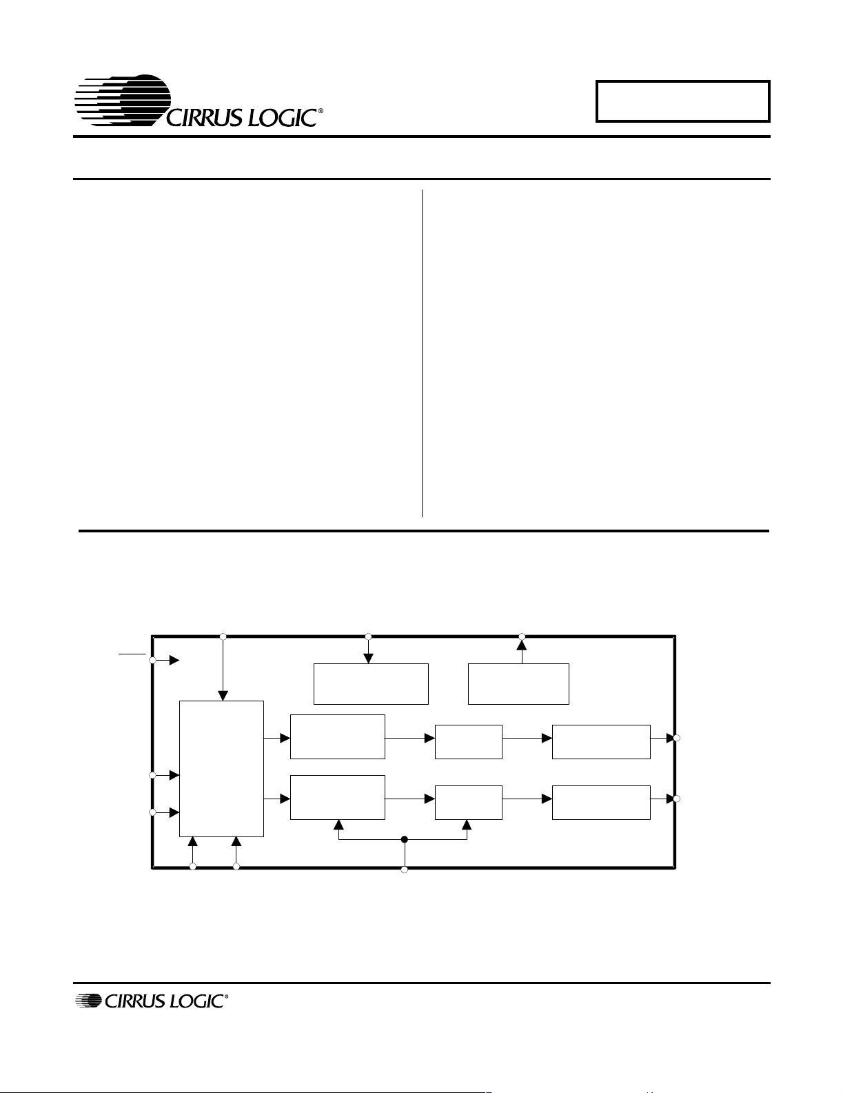
The CS4340A is a complete stereo digital-to-analog system including digital interpolation, fourth-order deltasigma digital-to-analog conversion, digital de-emphasis
and switched capacitor analog filtering. The advantages
of this architecture include: ideal differential linearity, no
distortion mechanisms due to resistor matching errors,
no linearity drift over time and temperature, and a high
tolerance to clock jitter.
The CS4340A accepts data at all standard audio sample
rates up to 192 kHz, consumes very little power, operates over a wide power supply range and is pin
compatible with the CS4340, as described in section 3.1.
These features are ideal for DVD audio players.
ORDERING INFORMATION
CS4340A-KS 16-pin SOIC, -10 to 70 °C
CS4340A-KSZ, Lead Free, 16-pin SOIC, -10 to 70 °C
CDB4340A Evaluation Board
RST
LRCK
SDIN
DIF0 DIF1
http://www.cirrus.com
SCLK
Serial
Audio
Interface
DEM
De-emphasis
Inter polation
Filter
Inter polation
Filter
Copyright © Cirrus Logic, Inc. 2005
∆Σ
DAC
∆Σ
DAC
MCLK
(All Rights Reserved)
MUTEC
External
Mute C ontrol
Analog Filter
Analog Filter
AOUT L
AOUTR
JULY '05
DS590F2
1
Page 2

TABLE OF CONTENTS
1. PIN DESCRIPTION ....................................................................................................................4
2. TYPICAL CONNECTION DIAGRAM......................................................................................5
3. APPLICATIONS .........................................................................................................................6
3.1 Upgrading from the CS4340 to the CS4340A .....................................................................6
3.2 Sample Rate Range/Operational Mode Detect ....................................................................6
3.3 System Clocking ..................................................................................................................6
3.4 Digital Interface Format.......................................................................................................7
3.5 De-Emphasis........................................................................................................................8
3.6 Power-up Sequence..............................................................................................................9
3.7 Popguard® Transient Control...............................................................................................9
3.7.1 Power-up.....................................................................................................................9
3.7.2 Power-down ................................................................................................................9
3.7.3 Discharge Time...........................................................................................................9
3.8 Mute Control......................................................................................................................10
3.9 Grounding and Power Supply Arrangements ....................................................................10
4. CHARACTERISTICS AND SPECIFICATIONS.....................................................................11
RECOMMENDED OPERATING SPECIFICATION .................................................................11
ABSOLUTE MAXIMUM RATINGS...........................................................................................11
ANALOG CHARACTERISTICS (CS4340A-KS/KSZ)...............................................................12
COMBINED INTERPOLATION & ON-CHIP ANALOG FILTER RESPONSE.......................14
SWITCHING SPECIFICATIONS - SERIAL AUDIO INTERFACE ..........................................17
DC ELECTRICAL CHARACTERISTICS ...................................................................................18
DIGITAL INTERFACE SPECIFICATIONS................................................................................18
DIGITAL INPUT CHARACTERISTICS .....................................................................................18
5. PARAMETER DEFINITIONS..................................................................................................19
6. REFERENCES...........................................................................................................................19
7. PACKAGE DIMENSIONS.......................................................................................................20
THERMAL CHARACTERISTICS AND SPECIFICATIONS ....................................................20
8. REVISION HISTORY...............................................................................................................21
CS4340A
2 DS590F2
Page 3

LIST OF FIGURES
CS4340A
Figure 1. Typical Connection Diagram..........................................................................................................5
Figure 2. CS4340A Format 0 - I
Figure 3. CS4340A Format 1 - Left Justified up to 24-Bit Data.....................................................................8
Figure 4. CS4340A Format 2 - Right Justified, 24-Bit Data ..........................................................................8
Figure 5. CS4340A Format 3 - Right Justified, 16-Bit Data ..........................................................................8
Figure 6. De-Emphasis Curve.......................................................................................................................8
Figure 7. Output Test Load.........................................................................................................................13
Figure 8. Maximum Loading........................................................................................................................13
Figure 9. Single-Speed Stopband Rejection...............................................................................................14
Figure 10. Single-Speed Transition Band...................................................................................................14
Figure 11. Single-Speed Transition Band (Detail).......................................................................................15
Figure 12. Single-Speed Passband Ripple.................................................................................................15
Figure 13. Double-Speed Stopband Rejection............................................................................................15
Figure 14. Double-Speed Transition Band..................................................................................................15
Figure 15. Double-Speed Transition Band (Detail).....................................................................................16
Figure 16. Double-Speed Passband Ripple................................................................................................16
Figure 17. Serial Input Timing.....................................................................................................................17
LIST OF TABLES
Table 1. CS4340A Auto-Detect.....................................................................................................................6
Table 2. Single-Speed Mode Standard Frequencies........... ... ... ... .... ... ... ................................................ ......7
Table 3. Double-Speed Mode Standard Frequencies...................................................................................7
Table 4. Quad-Speed Mode Standard Frequencies .....................................................................................7
Table 5. Digital Interface Format - DIF1 and DIF0........................................................................................7
Table 6. De-Emphasis Control......................................................................................................................8
2
S up to 24-Bit Data....................................................................................7
DS590F2 3
Page 4
1. PIN DESCRIPTION
CS4340A
SDIN AOUTL
SCLK VA
LRCK AGND
MCLK AOUTR
DIF1 REF_GND
DIF0 VQ
DEM FILT+
Pin Name # Pin Description
RST
SDIN
SCLK
LRCK
MCLK
DIF1
DIF0
DEM
FILT+
VQ
REF_GND
AOUTR
AOUTL
AGND
VA
MUTEC
Reset (Input) - Powers down device.
1
Serial Audio Data (Input) - Input for two’s complement serial audio data.
2
Serial Clock (Input) -Serial clock for the serial audio interface.
3
Left Right Clock (Input) - Determines which channel, Left or Right, is currently active on the
4
serial audio data line.
Master Clock (Input) - Clock source for the delta-sigma modulator and digital filters.
5
Digital Interface Format (Input) - Defines the required relationship between the Left Right
6
Clock, Serial Clock and Serial Audio Data.
7
De-emphasis Control (Input) - Selects the standard 15µs/50µs digital de-emphasis filter
8
response for the 44.1 kHz sample rate.
Positive Voltage Reference (Output) - Positive voltage reference for the internal
9
sampling circuits.
Quiescent Voltage (Output) - Filter connection for internal quiescent reference voltage.
10
Reference Ground (Input) - Ground reference for the internal sampling circuits.
11
Analog Outputs (Output) - The full scale analog output level is specified in the
12
Analog Characteristics table.
15
Analog Ground (Input)
13
14 Power (Input) - Positive power for the analog, digital and serial audio interface sections.
Mute Control (Output) - Control signal for an optional mute circuit.
16
RST MUTEC
161
152
143
134
125
116
107
98
4 DS590F2
Page 5
2. TYPICAL CONNECTION DIAGRAM
CS4340A
Serial Audio
Data
Processor
External Clock
Mode
Config urati on
1µF
560
560
+3.3V o r + 5 .0 V
Ω
C
+
1µF
0.1 µF
Ω
C
C=
OPTIONAL
MUTE
CIRCUIT
+ 560
R
L
π F
560
4
SRL
R
L
R
L
Left
Audio
Output
Right
Audio
Output
+
.1 µF
+
+
Ω
1µF
+
Ω
14
VA
2
SDIN
3
SCLK
4
LRCK
CS4340A
5
MCLK
6
DIF1
7
DIF0
8
DEM
1
RST
AGND
13
0.1µF
AOUT L
MUTEC
FILT+
VQ
REF_GND
AOUTR
3.3 µF
15
10 k
16
9
10
11
3.3 µF
12
10 k
Figure 1. Typical Connection Diagram
DS590F2 5
Page 6
CS4340A
3. APPLICATIONS
3.1 Upgrading from the CS4340 to the CS4340A
The CS4340A is pin and functionally compatible with all CS4340 designs, operating at the standard audio
sample rates, that use pin 3 as a serial clock input. In addition to the features of the CS4340, the CS4340A
supports standard sample rates up to 192 kHz, as well as automatic mode detection for sample rates between 4 and 200 kHz. The automatic mode detection feature allows sample rate changes between single,
double and quad-speed modes without external intervention.
The CS4340A does not support an internal serial clock mode, sample rates between 50 kHz and 84 kHz,
de-emphasis for 32 and 48 kHz, or 2.7 V operation as does the CS4340.
3.2 Sample Rate Range/Operational Mode Detect
The device operates in one of three operational modes. It will auto-detect the correct mode when the input
sample rate (Fs), defined by the LRCK frequency, falls within one of the ranges illustrated in Table 1. Sample rates outside the specified range for each mode are not supported.
Input Sample Rate (FS)MODE
4 kHz - 50 kHz Single-Speed Mode
84 kHz - 100 kHz Double-Speed Mode
170 kHz - 200 kHz Quad-Speed Mode
Table 1. CS4340A Auto-Detect
3.3 System Clocking
The device requires external generation of the master (MCLK), left/right (LRCK) and serial (SCLK)
clocks. The LRCK, defined also as the input sample rate (Fs), must be synchronously derived from the
MCLK according to specified ratios. The specified ratios of MCLK to LRCK, along with several standard
audio sample rates and the required MCLK frequency, are illustrated in Tables 2-4.
6 DS590F2
Page 7
CS4340A
Sample Rate
(kHz)
256x 384x 512x 768x
32 8.1920 12.2880 16.3840 24.5760
44.1 11.2896 16.9344 22.5792 33.8688
48 12.2880 18.4320 24.5760 36.8640
Table 2. Single-Speed Mode S tandard Frequencies
Sample Rate
(kHz)
88.2 11.2896 16.9344 22.5792 33.8688
96 12.2880 18.4320 24.5760 36.8640
Table 3. Double-Speed Mode Standard Frequencies
Sample Rate
(kHz)
176.4 22.5792 33.8688
192 24.5760 36.8640
Table 4. Quad-Speed Mode Standard Frequencies
3.4 Digital Interface Format
MCLK (MHz)
MCLK (MHz)
128x 192x 256x 384x
MCLK (MHz)
128x 192x
The device will accept audio samples in several digital interface formats as illustrated in Table 5. The desired format is selected via the DIF1 and DIF0 pins. For an illustration of the required relationship between
LRCK, SCLK and SDIN, see Figures 2-5.
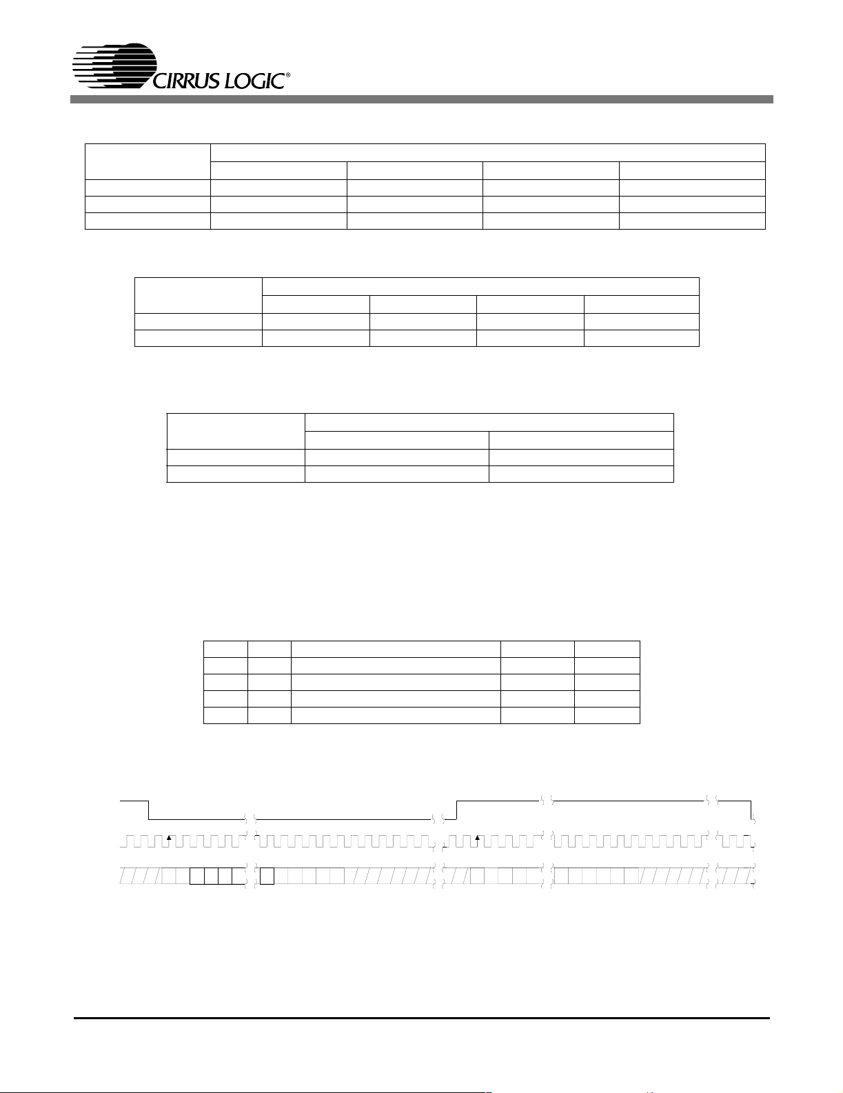
DIF1 DIF0 DESCRIPTION FORMAT FIGURE
00
01
10
11
LRCK
SCLK
SDIN +3 +2 +1+5 +4
MSB
-1 -2 -3 -4 -5
I2S, up to 24-bit data
Left Justified, up to 24-bit data
Right Justified, 24-bit Data
Right Justified, 16-bit Data
Table 5. Digital Interface Format - DIF1 and DIF0
Left C hannel
LSB
MSB LSB
-1 -2 -3 -4
Figure 2. CS4340A Format 0 - I2S up to 24-Bit Data
02
13
24
35
Right Channel
+3 +2 +1+5 +4
DS590F2 7
Page 8
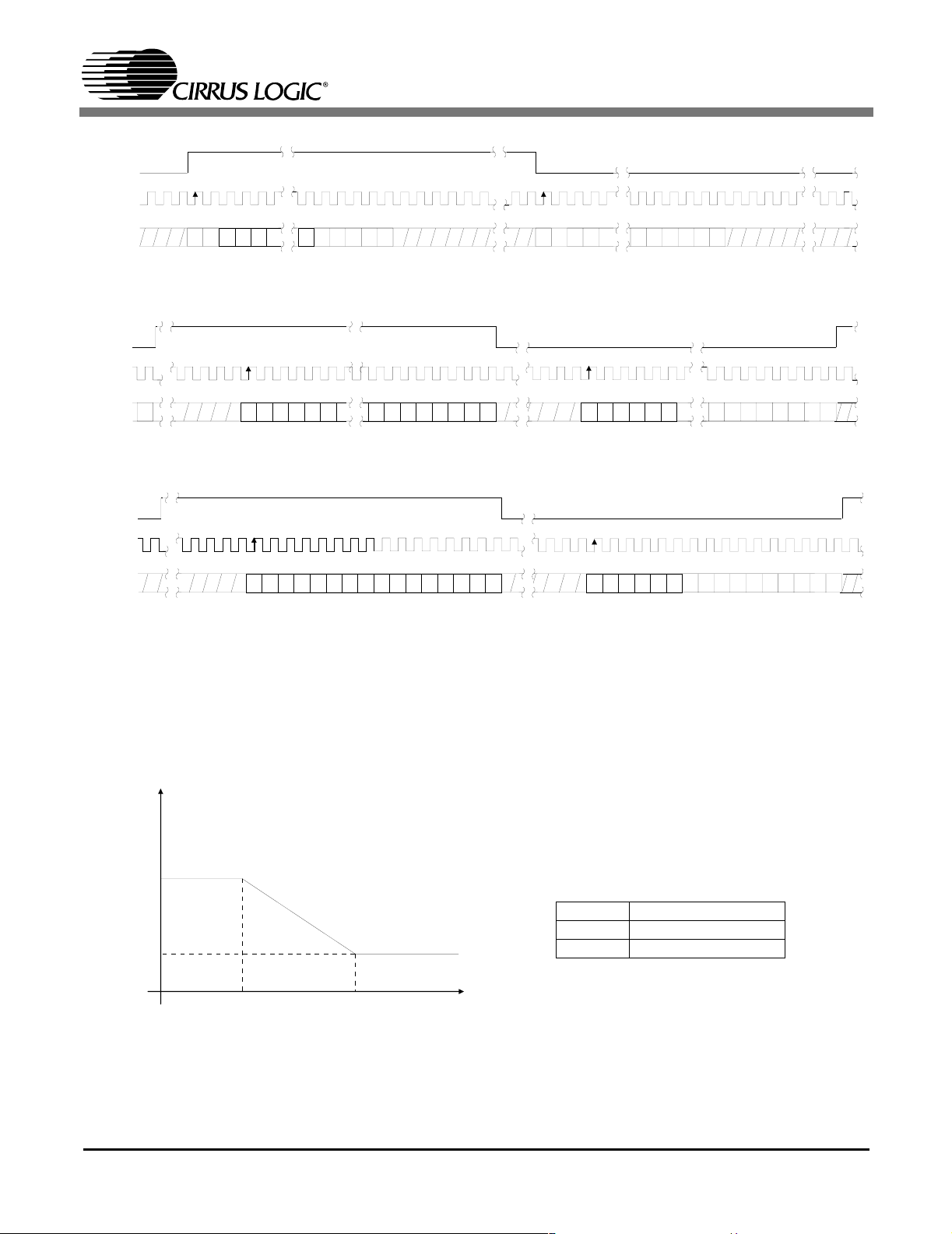
CS4340A
LRCK
SCLK
SDIN +3 +2 +1+5 +4
MSB
-1 -2 -3 -4 -5
Left C hannel
Figure 3. CS4340A Format 1 - Left Justified up to 24-Bit Data
LRCK
SCLK
SDIN
LRCK
SCLK
SDIN
0
Left Cha nnel
23 22 21 20 19 18
Figure 4. CS4340A Format 2 - Right Justified, 24-Bit Data
32 clocks
Left Cha nnel
15 14 13 12 11 10
LSB
Right Channel
LSB
MSB
-1 -2 -3 -4
65432107
6543210987
23 22 21 20 19 18
15 14 13 12 11 10
+3 +2 +1+5 +4
Right Channel
65432107
Right Channel
6543210987
Figure 5. CS4340A Format 3 - Right Justified, 16-Bit Data
32 clocks
3.5 De-Emphasis
The device includes on-chip digital de-emphasis. Figure 6 shows the de-emphasis curve for Fs equal to
44.1 kHz. The frequency response of the de-emphasis curve will scale proportionally with changes in sample rate, Fs. Please see Table 6 for the desired de-emphasis control.
Gain
dB
T1=50 µs
0dB
-10dB
F1 F2
3.183 kHz 10.61 kHz
Figure 6. De-Emphasis Curve
T2 = 15 µs
Frequency
DEM DESCRIPTION
0 Disabled
1 44.1 kHz
Table 6. De-Emphasis Control
8 DS590F2
Page 9

CS4340A
3.6 Power-up Sequence
Reliable power-up can be accomplished by keeping the device in reset until the power supply and configuration pins are stable, and the clocks are locked to the appropriate frequencies discussed in section 3.3. It
is also recommended that reset be enabled if the analog supply drops below the minimum specified operating voltage to prevent power glitch related issues.
3.7 Popguard® Transient Control
The CS4340A uses Popguard® technology to minimize the effects of output transients during power-up
and power-down. This technology, when used with external DC-blocking capacitors in series with the audio outputs, minimizes the audio transients commonly produced by single-ended single-supply converters.
It is activated inside the DAC when RST
from choosing the appropriate DC-blocking capacitors.
3.7.1 Power-up
When the device is initially powered-up, the audio outputs, AOUTL and AOUTR, are clamped to
AGND. Following a delay of approximately 1000 sample periods, each output begins to ramp toward the quiescent voltage. Approximately 10,000 LRCK cycles later, the outputs reach VQ and
audio output begins. This gradual voltage ramping allows time for the external DC-blocking capacitors to charge to the quiescent voltage, minimizing the power-up transient.
is enabled/disabled and requires no other external control, aside
3.7.2 Power-down
To prevent transients at power-down, the device must first enter its power-down state by enabling
RST. When this occurs, audio output ceases and the internal output buffers are disconnected from
AOUTL and AOUTR. In their place, a soft-start current sink is substituted which allows the DCblocking capacitors to slowly discharge. Once this charge is dissipated, the power to the device
may be turned off and the system is ready for the next power-on.
3.7.3 Discharge Time
To prevent an audio transient at the next power-on, it is necessary to ensure that the DC-blocking
capacitors have fully discharged before turning on the power or exiting the power-down state. If
not, a transient will occur when the audio outputs are initially clamped to AGND. The time that the
device must remain in the power-down state is related to the value of the DC-blocking capacitance.
For example, with a 3.3 µF capacitor, the minimum power-down time will be approximately
0.4 seconds.
DS590F2 9
Page 10

CS4340A
3.8 Mute Control
The Mute Control pin goes high during power-up initialization, reset, or if the MCLK to LRCK ratio is
incorrect. The pin will also go high following the reception of 8192 consecutive audio samples of static 0
or -1 on both the left and right channels. A single sample of non-zero data on either channel will cause the
Mute Control pin to go low. This pin is intended to be used as a control for an external mute circuit to prevent the clicks and pops that can occur in any single-ended single supply system.
Use of the Mute Control function is not mandatory but recommended for designs requiring the absolute
minimum in extraneous clicks and pops. Also, use of the Mute Control function can enable the system designer to achieve idle channel noise/signal-to-noise ratios which are only limited by the external mute circuit. See the CDB4340A data sheet for a suggested mute circuit.
3.9 Grounding and Power Supply Arrangements
As with any high resolution converter, the CS4340A requires careful attention to power supply and
grounding arrangements if its potential performance is to be realized. Figure 1 shows the recommended
power arrangements, with VA connected to a clean supply. If the ground planes are split between digital
ground and analog ground, REF_GND & AGND should be connected to the analog ground plane.
Decoupling capacitors should be as close to the DAC as possible, with the low value ceramic capacitor
being the closest. To further minimize impedance, these capacitors should be located on the same layer as
the DAC.
All signals, especially clocks, should be kept away from the FILT+ and VQ pins in order to avoid unwanted coupling into the modulators. The FILT+ and VQ decoupling capacitors, particularly the 0.1 µF, must
be positioned to minimize the electrical path from FILT+ and REF_GND (as well as VQ and REF_GND),
and should also be located on the same layer as the DAC. The CDB4340A evaluation board demonstrates
the optimum layout and power supply arrangements.
10 DS590F2
Page 11

CS4340A
4. CHARACTERISTICS AND SPECIFICATIONS
(Min/Max performance characteristics and specifications are guaranteed over the Specified Operating Conditions.
Typical performance characteristics are derived from measurements taken at T
RECOMMENDED OPERATING SPECIFICATION
Parameters Symbol Min Typ Max Units
DC Power Supply
3.3 V Nominal
5.0 V Nominal
Ambient Operating Temperature (Power Applied) T
VA 3.0
A
= 25°C.)
A
3.3
4.5
-10 - +70 °C
5
3.6
5.5
V
V
ABSOLUTE MAXIMUM RATINGS
beyond these limits may result in permanent damage to the device. Normal operation is not guaranteed at these
extremes.)
Parameters Symbol Min Max Units
DC Power Supply VA -0.3 6.0 V
Input Current
Digital Input Voltage V
Ambient Operating Temperature (power applied) T
Storage Temperature T
1.Any pin except supplies.
(AGND = 0 V; all voltages with respect to AGND. Operation
(Note 1) I
in
IND
A
stg
-±10mA
-0.3 VA+0.4 V
-55 125 °C
-65 150 °C
DS590F2 11
Page 12

CS4340A
ANALOG CHARACTERISTICS (CS4340A-KS/KSZ) (Test conditions (unless otherwise
specified): Input test signal is a 997 Hz sine wave; measurement bandwidth is 10 Hz to 20 kHz; test load
=10kΩ, CL= 10 pF (see Figure 7).)
R
L
VA = 5.0 V VA = 3.3 V
Parameter
Single-Speed Mode Fs = 48 kHz
Dynamic Range
(Note 2)
18 to 24-Bit unweighted
A-Weighted
16-Bit unweighted
A-Weighted
Total Harmonic Distortion + Noise
(Note 2)
18 to 24-Bit 0 dB
-20 dB
-60 dB
16-Bit 0 dB
-20 dB
-60 dB
Double-Speed Mode Fs = 96 kHz
Dynamic Range
(Note 2)
18 to 24-Bit unweighted
A-Weighted
16-Bit unweighted
A-Weighted
Total Harmonic Distortion + Noise
(Note 2)
18 to 24-Bit 0 dB
-20 dB
-60 dB
16-Bit 0 dB
-20 dB
-60 dB
Quad-Speed Mode Fs = 192 kHz
Dynamic Range
(Note 2)
18 to 24-Bit unweighted
A-Weighted
16-Bit unweighted
A-Weighted
Total Harmonic Distortion + Noise
(Note 2)
18 to 24-Bit 0 dB
-20 dB
-60 dB
16-Bit 0 dB
-20 dB
-60 dB
Min Typ Max Min Typ Max Unit
92
95
92
95
92
95
88
98
101
-
-
-
-
-
-
-
-
92
95
-91
-78
-38
-90
-72
-32
98
101
-
-
-
-
-
-
-
-
92
95
-91
-78
-38
-90
-72
-32
98
101
-
-
-
-
-
-
-
-
92
95
-91
-78
-38
-90
-72
-32
-
-
-
-
-85
-
-
-
-
-
-
-
-
-
-85
-
-
-
-
-
-
-
-
-
-85
-
-
-
-
-
91
88
91
88
91
94
97
92
95
-
-94
-
-74
-
-34
-
-91
-
-72
-
-32
-
94
97
92
95
-
-94
-
-74
-
-34
-
-91
-
-72
-
-32
-
94
97
92
95
-
-94
-
-74
-
-34
-
-91
-
-72
-
-32
-
-
-
-
-
-88
-
-
-
-
-
-
-
-
-
-88
-
-
-
-
-
-
-
-
-
-88
-
-
-
-
-
dB
dB
dB
dB
dB
dB
dB
dB
dB
dB
dB
dB
dB
dB
dB
dB
dB
dB
dB
dB
dB
dB
dB
dB
dB
dB
dB
dB
dB
dB
12 DS590F2
Page 13

CS4340A
ANALOG CHARACTERISTICS (CS4340A-KS/KSZ) (Continued)
Parameters Symbol Min Typ Max Units
Dynamic Performance for All Modes
Interchannel Isolation (1 kHz) - 102 - dB
DC Accuracy
Interchannel Gain Mismatch - 0.1 - dB
Gain Drift - ±100 - ppm/°C
Analog Output Characteristics and Specifications
Full Scale Output Voltage 0.6•VA 0.7•VA 0.8•VA Vpp
Output Impedance - 100 - Ω
Minimum AC-Load Resistance
Maximum Load Capacitance
Notes: 2. One-half LSB of triangular PDF dither is added to data.
3. Refer to Figure 8.
(Note 3) R
(Note 3) C
.
L
L
-3-kΩ
- 100 - pF
AGND
3.3 µF
AOUTx
+
Figure 7. Output Test Load
125
100
V
out
R
L
C
L
L
75
50
25
Capacitive Load -- C (pF)
2.5
51015
3
Safe Operating
Region
Resistive Load -- R (kΩ)
L
20
Figure 8. Maximum Loading
DS590F2 13
Page 14
CS4340A
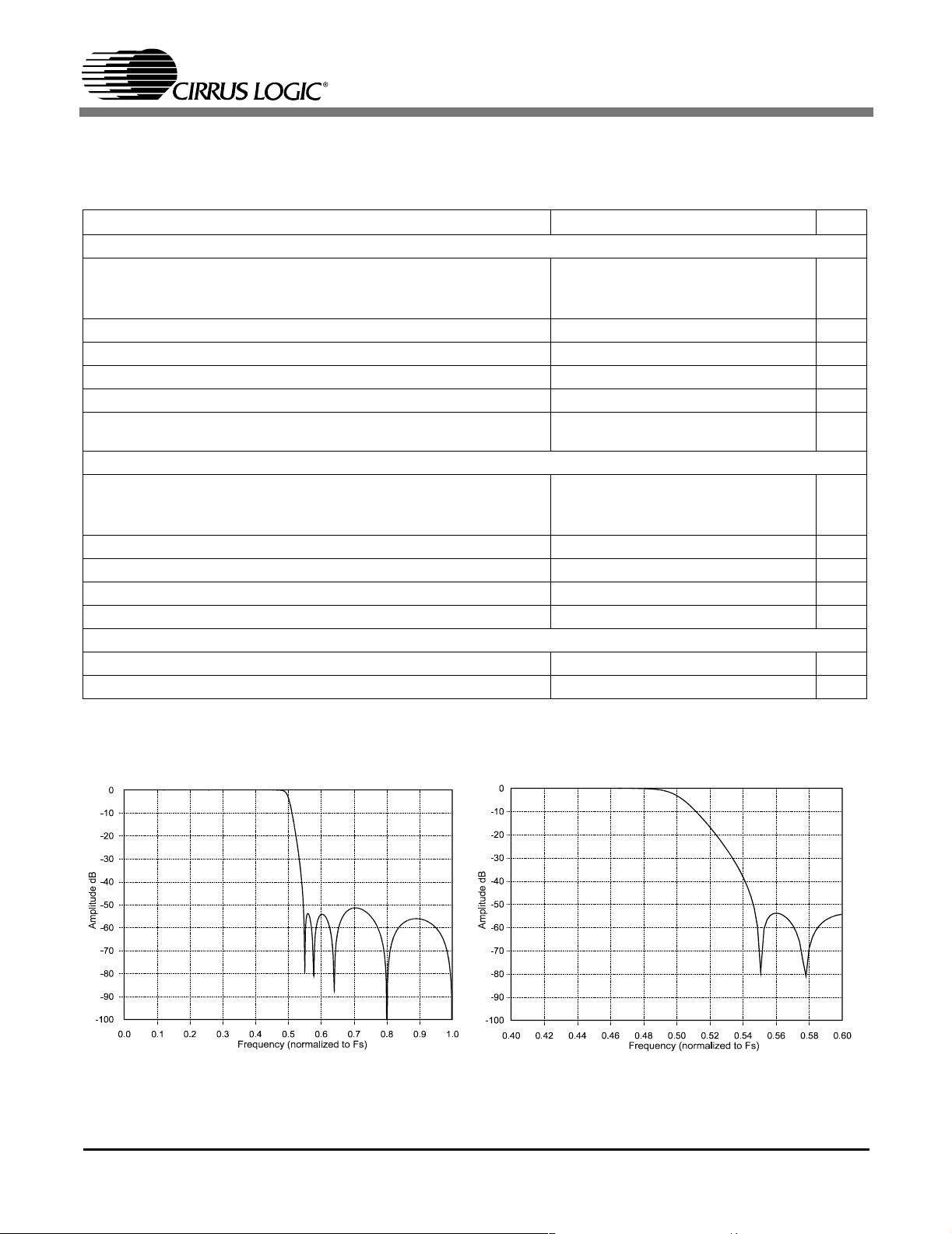
COMBINED INTERPOLATION & ON-CHIP ANALOG FILTER RESPONSE (The
filter characteristics and the X-axis of the response plots have been normalized to the sample rate (Fs) and can be
referenced to the desired sample rate by multiplying the given characteristic by Fs.)
Parameter Min Typ Max Unit
Single-Speed Mode - (4 kHz to 50 kHz sample rates)
Passband
to -0.05 dB corner
to -3 dB corner
Frequency Response 10 Hz to 20 kHz -0.02 - +0.08 dB
StopBand 0.5465 - - Fs
StopBand Attenuation
Group Delay - 9/Fs - s
De-emphasis Error (Relative to 1 kHz) Fs = 44.1 kHz
(Note 5)
Double-Speed Mode - (84 kHz to 100 kHz sample rates)
Passband
to -0.1 dB corner
to -3 dB corner
Frequency Response 10 Hz to 20 kHz -0.06 - +0.2 dB
StopBand 0.577 - - Fs
StopBand Attenuation
Group Delay - 4/Fs - s
Quad-Speed Mode - (170 kHz to 200 kHz sample rates)
Frequency Response 10 Hz to 20 kHz -1 - 0 dB
Group Delay - 3/Fs - s
(Note 4) 50 - - dB
(Note 4) 55 - - dB
0
0
--+0.05/-0.14dB
0
0
-
-
-
-
0.4535
0.4998
0.4621
0.4982
Fs
Fs
Fs
Fs
Notes: 4. For Single-Speed Mode, the measurement bandwidth is 0.5465 Fs to 3 Fs.
For Double-Speed Mode, the measurement bandwidth is 0.577 Fs to 1.4 Fs.
5. De-emphasis is only available in Single-Speed Mode.
Figure 9. Single-Speed Stopband Rejection Figure 10. Single-Speed Transition Band
14 DS590F2
Page 15

CS4340A
Figure 11. Single-Speed Transition Band (Detail) Figure 12. Single-Speed Passband Ripple
Figure 13. Double-Speed Stopband Rejection Figure 14. Double-Speed Transition Band
DS590F2 15
Page 16

CS4340A
Figure 15. Double-Speed Transition Band (Detail) Figure 16. Double-Speed Passband Ripple
16 DS590F2
Page 17

CS4340A
SWITCHING SPECIFICATIONS - SERIAL AUDIO INTERFACE
Parameters Symbol Min Max Units
MCLK Frequency 1.024 38.4 MHz
MCLK Duty Cycle 45 55 %
Input Sample Rate Single-Speed Mode
(Note 6) Double-Speed Mode
Quad-Speed Mode
Fs
Fs
Fs
4
84
170
50
100
200
kHz
kHz
kHz
LRCK Duty Cycle 40 60 %
SCLK Frequency Single-Speed Mode
Double-Speed Mode
Quad-Speed Mode
SCLK Pulse Width Low t
SCLK Pulse Width High t
SCLK rising to LRCK edge delay t
SCLK rising to LRCK edge setup time t
SDIN valid to SCLK rising setup time t
SCLK rising to SDIN hold time t
SCLK rising to MCLK edge delay (Note 7) t
sclkl
sclkh
slrd
slrs
sdlrs
sdh
smd
-
-
-
128xFs
64xFs
MCLK
----------------- -
2
20 - ns
20 - ns
20 - ns
20 - ns
20 - ns
20 - ns
8-ns
Notes: 6. Speed mode is detected automatically, based on the input sample rate.
7. Only required for Quad-Speed Mode.
Hz
Hz
Hz
MCLK
LRCK
SCLK
SDATA
t
t
slrd
smd
t
sdlrs
Figure 17. Serial Input Timing
t
slrs
t
sclkl
t
sdh
t
sclkh
DS590F2 17
Page 18

CS4340A
DC ELECTRICAL CHARACTERISTICS (AGND = 0 V; all voltages with respect to AGND.)
Parameters Symbol Min Typ Max Units
Normal Operation
Power Supply Current VA = 5.0 V
Power Dissipation VA = 5.0 V
Power-down Mode
Power Supply Current VA = 5.0 V
VA = 3.3 V
Power Dissipation VA = 5.0 V
All Modes of Operation
Power Supply Rejection Ratio
V
Nominal Voltage
Q
Output Impedance
Maximum allowable DC current source/sink
Filt+ Nominal Voltage
Output Impedance
Maximum allowable DC current source/sink
MUTEC Low-Level Output Voltage - 0 - V
MUTEC High-Level Output Voltage - VA - V
Maximum MUTEC Drive Current - 3 - mA
(Note 8)
(Note 9)
VA = 3.3 V
VA = 3.3 V
VA = 3.3 V
(Note 10) 1 kHz
60 Hz
I
A
I
A
PSRR -
-
-
-
-
-
-
-
-
-
-
-
-
-
-
-
18
15
90
50
60
35
0.3
0.1
60
40
0.5•VA
250
0.01
VA
250
0.01
25
20
125
100
-
-
-
-
-
-
-
-
-
-
-
-
mA
mA
mW
mW
µA
µA
mW
mW
dB
dB
kΩ
mA
kΩ
mA
V
V
DIGITAL INTERFACE SPECIFICATIONS (GND = 0 V; all voltages with respect to GND.)
Parameters Symbol Min Max Units
3.3 V Logic (2.7 V to 3.6 V DC Supply)
High-Level Input Voltage V
Low-Level Input Voltage V
IH
IL
2.0 - V
-0.8V
5.0 V Logic (4.5 V to 5.5 V DC Supply)
High-Level Input Voltage V
Low-Level Input Voltage V
IH
IL
2.0 - V
-0.8V
DIGITAL INPUT CHARACTERISTICS (AGND = 0 V; all voltages with respect to AGND.)
Parameters Symbol Min Typ Max Units
Input Leakage Current I
in
Input Capacitance - 8 - pF
Notes: 8. Normal operation is defined as RST
= HI with a 997 Hz, 0 dBFS input sampled at the highest Fs for each
speed mode, and open outputs, unless otherwise specified.
9. Power Down Mode is defined as RST
= LO with all clocks and data lines held static.
10. Valid with the recommended capacitor values on FILT+ and VQ as shown in Figure 1. Increasing the
capacitance will also increase the PSRR.
--±10µA
18 DS590F2
Page 19

5. PARAMETER DEFINITIONS
Total Harmonic Distortion + Noise (THD+N)
The ratio of the rms value of the signal to the rms sum of all other spectral components over the specified
bandwidth (typically 10 Hz to 20 kHz), including distortion components. Expressed in decibels.
Dynamic Range
The ratio of the full scale rms value of the signal to the rms sum of all other spe ctral components over the
specified bandwidth. Dynamic range is a signal-to-noise measurement over the specified bandwidth
made with a -60 dBFS signal. 60 dB is then adde d to the resulting measurement to refer the measurement
to full scale. This technique ensures that the distortion components are below the noise level and do not
affect the measurement. This measurement technique has been accepted by the Audio Engineering Society, AES17-1991, and the Electronic Industries Association of Japan, EIAJ CP-307.
Interchannel Isolation
A measure of crosstalk between the left and right channels. Mea sured for each channel at the converter’s
output with all zeros to the input under test and a full-scale signal applied to the other channel. Units in
decibels.
Interchannel Gain Mismatch
The gain difference between left and right channels. Units in decibels.
CS4340A
Gain Drift
The change in gain value with temperature. Units in ppm/°C.
6. REFERENCES
1) CDB4340A Evaluation Board Datasheet
DS590F2 19
Page 20

7. PACKAGE DIMENSIONS
16L SOIC (150 MIL BODY) PACKAGE DRAWING
1
b
CS4340A
E
H
c
∝
L
SEATING
PLANE
D
A
e
A1
INCHES MILLIMETERS
DIM MIN NOM MAX MIN NOM MAX
A 0.053 0.064 0.069 1.35 1.63 1.75
A1 0.004 0.006 0.010 0.10 0.15 0.25
b 0.013 0.016 0.020 0.33 0.41 0.51
C 0.0075 0.008 0.010 0.19 0.20 0.25
D 0.386 0.390 0.394 9.80 9.91 10.00
E 0.150 0.154 0.157 3.80 3.90 4.00
e 0.040 0.050 0.060 1.02 1.27 1.52
H 0.228 0.236 0.244 5.80 6.0 6.20
L 0.016 0.025 0.050 0.40 0.64 1.27
∝ 0° 4° 8° 0° 4° 8°
JEDEC #: MS-012
Controling Dimension is Millimeters
THERMAL CHARACTERISTICS AND SPECIFICATIONS
Parameters Symbol Min Typ Max Units
Package Thermal Resistance
20 DS590F2
(multi-layer boards) θ
JA
-74-°C/Watt
Page 21

8. REVISION HISTORY
Release Date Changes
F2 July 2005 Added Revision History table and updated ordering information.
CS4340A
Contacting Cirrus Logic Support
For all product questions and inquiries contact a Cirrus Logic Sales Representative.
To find one nearest you go to www.cirrus.com
IMPORTANT NOTICE
Cirrus Logic, Inc. and its subsidiaries ("Cirrus") believe that the informatio n contained in this docum ent is accura te and relia ble. How ever, the in formation is sub-
ject to change without notice and is provided "AS IS" without warranty of any kind (express or implied). Customers are advised to obtain the latest version of
relevant information to verify, before placing orders, that information being relied on is current and complete. All products are sold subject to the terms and conditions of sale supplied at the time of order acknowledgment, including those pertaining to warranty, indemnification, and limitation of liability. No responsibility
is assumed by Cirrus for the use of t his i nformati on, incl uding use o f this in formati on as the basis for manufact ure or s ale of any items, or for infringement of
patents or other ri ghts of third p arties. This doc ument is t he propert y of Ci rrus an d by furn ishing t his inf ormation , Cirrus grants no license, express or implied
under any patents, mask work ri g hts , copy ri gh t s, tr ad emar ks, tr ade sec ret s o r other intellectual proper t y ri gh ts . Ci rr us owns t he copyrights associated with the
information contained herein and gives consent for copies to be made of the information only for use within your organization with respect to Cirrus integrated
circuits or other products of Cirrus. This consent does not extend to other copying such as copying for general distribution, advertising or promotional purposes,
or for creating any work for resale.
CERTAIN APPLICATIONS USING SEMICONDUCTOR PRODUCTS MAY INVOLVE POTENTIAL RISKS OF DEATH, PERSONAL INJURY, OR SEVERE
PROPERTY OR ENVIRONMENTAL DAMAGE (“CRITICAL APPLICATIONS”). CIRRUS PRODUCTS ARE NOT DESIGNED, AUTHORIZED OR WARRANTED FOR USE IN AIRCRAFT SYSTEMS, MILITARY AP PLICATIONS, PRODUC TS SURGICALLY IMPLANT ED INTO THE BODY, AU TOMOTIVE SAFETY OR
SECURITY DEVICES, LIFE SUPPORT PRODUCTS OR OTHER CRITICAL APPLICATIONS. INCLUSION OF CIRRUS PRODUCTS IN SUCH APPLICATIONS IS UNDERSTOOD TO BE FULLY AT THE CUSTOMER’S RISK AND CIRRUS DISCLAIMS AND MAKES NO WARRANTY, EXPRESS, STATUTORY
OR IMPLIED, INCLUDING THE IMPLIED WARRANTIES OF MERCHANTABILITY AND FITNESS FOR PARTICULAR PURPOSE, WITH REGA RD TO ANY
CIRRUS PRODUCT THAT IS USED IN SUCH A MANNER. IF THE CUSTOMER OR CUSTOMER’S CUSTOMER USES OR PERMITS THE USE OF CIRRUS
PRODUCTS IN CRITICAL APPLICATIONS, CUS TOMER AGREES, BY SUCH USE, TO FULLY INDEMNIFY CIRRUS, ITS OFFICERS, DIRECTORS, EMPLOYEES, DISTRIBUTORS AND OTHER AGE NTS FROM ANY AND AL L L I ABI LI TY, I NCLUDING AT TORNEYS’ F EES AND COST S, T HAT MA Y RESUL T
FROM OR ARISE IN CONNECTION WITH THESE USES.
Cirrus Logic, Cirrus, the Cirrus Logic logo designs, and Popguard are trademarks of Cirrus Logic, Inc. All other brand and product names in this document may
be trademarks or service marks of their respective owne rs.
DS590F2 21
 Loading...