

Page 1
CS4340
24-Bit, 96 kHz Stereo D/A Converter for Audio
Features
! 101 dB Dynamic Range
! -91 dB THD+N
! +3.0 V or +5.0 V Power Supply
! Low Clock Jitter Sensitivity
! Filtered Line-level Outputs
! On-chip Digital De-emphasis for 32, 44.1 and
48 kHz
! 33 mW with 3V Supply
! Popguard
®
Technology for Control of Clicks
and Pops
! Lead-free Packaging Available
Description
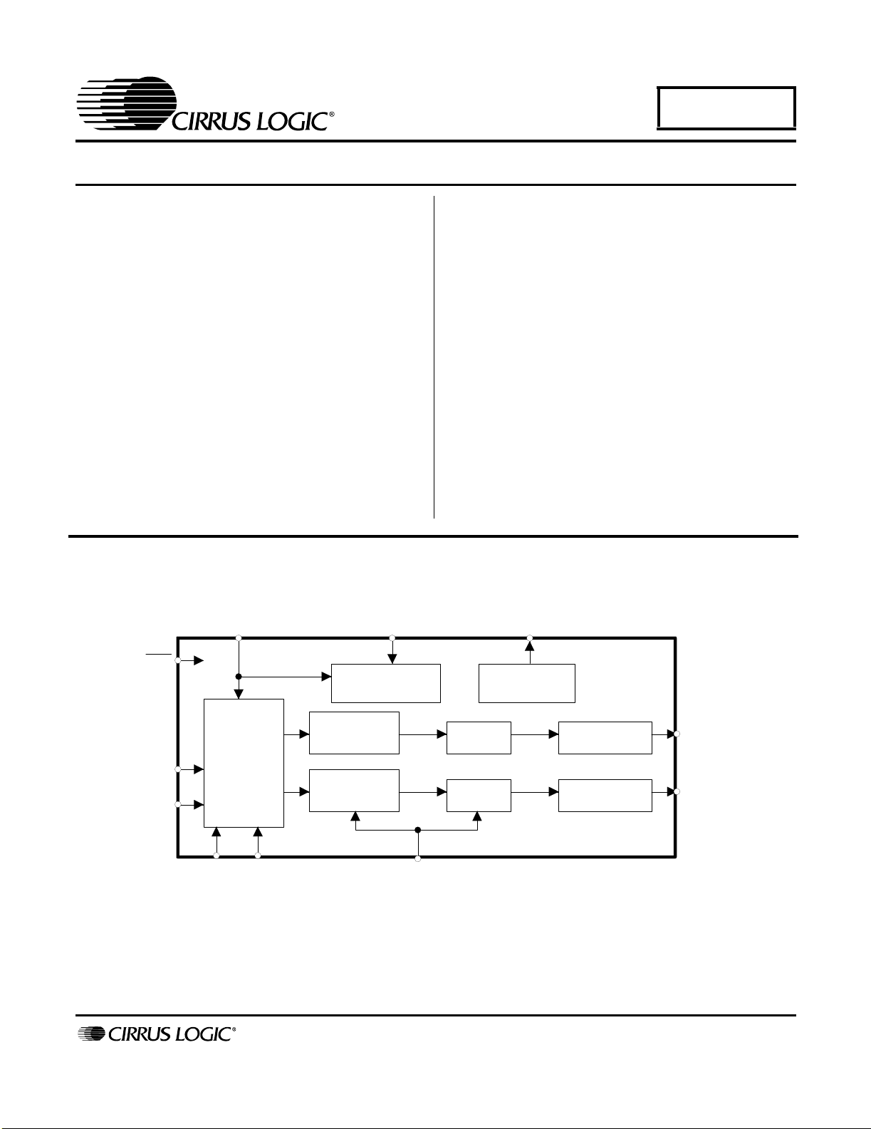
The CS4340 is a complete stereo digital-to-analog system
including digital interpolation, fourth-order delta-sigma dig-
I
ital-to-analog conversion, digital de-emphasis and
switched capacitor analog filtering. The advantages of this
architecture include: ideal differential linearity, no distortion mechanisms due to resistor matching errors, no
linearity drift over time and temperature and a high tolerance to clock jitter.
The CS4340 accepts data at audio sample rates from
4 kHz to 100 kHz, consumes very little power, and operates over a wide power supply range. The features of the
CS4340 are ideal for DVD players, CD players, set-to p box
and automotive systems.
ORDERING INFORMATION
CS4340-DSZ 16-pin SOIC, Lead Free, -40 to 85 °C
CS4340-KS 16-pin SOIC -10 to 70 °C
CS4340-KSZ 16-pin SOIC, Lead Free, -10 to 70 °C
CS4340-CZZ 16-pin TSSOP, Lead Free, -10 to 70 °C
CDB4340 Evaluation Board
RST
LRCK
SDATA
SCLK/DEM1
Serial
Input
Interface
DIF0
DIF1
DEM0
De-emphasis
Interpolation
Filter
Interpolation
Filter
MCLK
Mute Control
DAC
∆Σ
DAC
∆Σ
MUTEC
External
Analog Filter
Analog Filter
AOUTL
AOUTR
www.cirrus.com
Copyright © Cirrus Logic, Inc. 2005
(All Rights Reserved)
JULY '05
DS297F3
1
Page 2
TABLE OF CONTENTS
1. CHARACTERISTICS AND SPECIFICATIONS ..................................................................................... 4
SPECIFIED OPERATING CONDITIONS.............................................................................................. 4
ABSOLUTE MAXIMUM RATINGS ........................................................................................................4
ANALOG CHARACTERISTICS (CS4340-KS/KSZ/CZZ)....................................................................... 5
ANALOG CHARACTERISTICS (CS4340-DSZ).................................................................................... 7
COMBINED INTERPOLATION & ON-CHIP ANALOG FILTER RESPONSE........................................ 8
SWITCHING SPECIFICATIONS - SERIAL AUDIO INTERFACE........................................................ 11
SWITCHING CHARACTERISTICS - INTERNAL SERIAL CLOCK ..................................................... 12
DC ELECTRICAL CHARACTERISTICS.............. ... ... .... ... ... ... .......................................... ... ................ 13
DIGITAL INPUT CHARACTERISTICS ................................................................................................ 13
DIGITAL INTERFACE SPECIFICATIONS........................................................................................... 13
2. PIN DESCRIPTION .............................................................................................................................. 14
3. TYPICAL CONNECTION DIAGRAM ................................................................................................. 15
4. APPLICATIONS ................................................................................................................................... 16
4.1 Sample Rate Range/Operational Mode ........................................................................................ 16
4.2 System Clocking .................... .... ... ... ... ... .... ...................................... .... ... ... ... ................................ 16
4.2.1 Internal Serial Clock Mode ...............................................................................................16
4.2.2 External Serial Clock Mode .............................................................................................. 17
4.3 Digital Interface Format ................................................................................................................. 17
4.4 De-Emphasis ...................................................... .... ... ... ... ....................................... ... ................... 18
4.5 Power-up Sequence .................................................................................................................... 19
4.6 Popguard
4.6.1 Power-up ....................... ... ... ....................................... ... ... ................................................ 19
4.6.2 Power-down ........................................... .... ... ....................................... ... ... ...................... 19
4.6.3 Discharge Time ............................................. ... ... .... ...................................... ... .... ... ......... 19
4.7 Mute Control ....................................................... ....................................... ... .... ... ... ...................... 20
4.8 Grounding and Power Supply Arrangements ............................................................................... 20
®
Transient Control .............................. .... ... ... ... .... ... ... ... ... .... ... ... ... ................................ 19
CS4340
Contacting Cirrus Logic Support
For all product questions and inquiries contact a Cirrus Logic Sales Representative.
To find one nearest you go to www.cirrus.com
IMPORTANT NOTICE
Cirrus Logic, Inc. and it s su bsi di ar i es ( " Ci r ru s" ) bel i eve that the information cont ai ne d in thi s docu ment is acc ura t e and r el iable. However, the inf o rmat io n i s subj ec t
to change without not ice and i s provi ded "AS I S" witho ut warrant y of an y kind ( express o r implie d). Cust omers are a dvised t o obtain the latest version of relevant
information to verify, before placing orders, that information being relied on is current and complete. All products are sold subject to the terms and conditions of sale
supplied at the time of order acknowledgment, including those pertaining to warranty, indemnification, and limitation of liability. No responsibility is assumed by Cirrus
for the use of this information, incl uding use of th is inform ation as the basis for ma nufacture or sa le of any item s, or for in fringement of patents or other rights of third
parties. This document is the property of Cirru s and by furnishing this information, Cirrus gran ts no license, express or implied under any patents, mask wo rk r ights,
copyrights, trademarks, trade secrets or other intellectual property rights. Cirrus owns the copyrights associated with the information contained herein and gives consent for copies to be made of the i nformation only for use within your organization wit h respect to Cirrus integrated circuits or other products of Cirrus. This consent
does not extend to other copying such as copying for general distribution, advertising or promotio na l pu rposes, or for creating any work for re s al e.
CERTAIN APPLICATIONS USING SEMI CONDUCTOR P RODUCT S MAY I NVOL VE PO TENT I AL RI SKS OF DEAT H, PE RS ONAL IN JU RY, OR S EV ERE PRO PERTY OR ENVIRONMENTAL DAMAGE (“CRITICAL APPLICATIONS”). CIRRUS PRODUCTS ARE NOT DESIGNED, AUTHORIZED OR WARRANTED FOR USE
IN AIRCRAFT SYSTEMS, MILITARY APPLICATIONS, PRODUCTS SURGICALLY IMPLANTED INTO THE BODY, AUTOMOTIVE SAFETY OR SECURITY DEVICES, LIFE SUPPORT PRODUCTS OR OTHER CRITICAL APPLICATIONS. INCLUSION OF CIRRUS PRODUCTS IN SUCH APPLICATIONS IS UNDERSTOOD
TO BE FULLY AT THE CUSTOMER’S RISK AND CIRRUS DISCLAIMS AND MAKES NO WARRANTY, EXPRESS, STATUTORY OR IMPLIED, INCLUDING THE
IMPLIED WARRANTIES OF MERCHANTABILITY AND FITNESS FOR PARTICULAR PURPOSE, WITH REGARD TO ANY CIRRUS PRODUCT THAT IS USED
IN SUCH A MANNER. IF THE CUSTOMER OR CUSTOMER’S CUSTOMER USES OR PERMITS THE USE OF CIRRUS PRODUCTS IN CRITICAL APPLICATIONS, CUSTOMER AGREES, BY SUCH USE, TO FULLY INDEMNIFY CIRRUS, ITS OFFICERS, DIRECTORS, EMPLOYEES, DISTRIBUTORS AND OTHER
AGENTS FROM ANY AND ALL LIABILITY, INCLUDING ATTORNEYS’ FEES AND COSTS, THAT MAY RESULT FROM OR ARISE IN CONNECTION WITH
THESE USES.
Cirrus Logic, Cirrus, and the Cirrus Logic logo designs are trademarks of Cirrus Logic, Inc. All other brand and product names in this document may be trade marks
or service marks of their respective owners.
2 DS297F3
Page 3

5. PARAMETER DEFINITIONS ................................................................................................................21
6. REFERENCES ......................................................................................................................................22
7. PACKAGE DIMENSIONS ....................................................................................................................23
7.1 SOIC ................... ....................................... ... ... ....................................... ... ... .................................23
7.2 TSSOP ............................ ... ... .... ...................................... .... ... .......................................................24
8. PACKAGE THERMAL RESISTANCE .................................................................................................25
LIST OF FIGURES
Figure 1. Output Test Load...........................................................................................................................6
Figure 2. Maximum Loading..........................................................................................................................6
Figure 3. Single-Speed Stopband Rejection.................................................................................................9
Figure 4. Single-Speed Transition Band.......................................................................................................9
Figure 5. Single-Speed Transition Band (Detail)...........................................................................................9
Figure 6. Single-Speed Passband Ripple.....................................................................................................9
Figure 7. Double-Speed Stopband Rejection................................................................................................9
Figure 8. Double-Speed Transition Band......................................................................................................9
Figure 9. Double-Speed Transition Band (Detail).......................................................................................10
Figure 10. Double-Speed Passband Ripple................................................................................................10
Figure 11. Serial Input Timing (External SCLK)..........................................................................................11
Figure 12. Internal Serial Mode Input Timing..............................................................................................12
Figure 13. Internal Serial Clock Generation................................................................................................12
Figure 14. Typical Connection Diagram......................................................................................................15
Figure 15. CS4340 Format 0 - I
Figure 16. CS4340 Format 1 - Left Justified up to 24-Bit Data......... ... ... ... ... .... ... ... ....................................17
Figure 17. CS4340 Format 2 - Right Justified, 24-Bit Data............................................................ ... ... ... ....18
Figure 18. CS4340 Format 3 - Right Justified, 16-Bit Data............................................................ ... ... ... ....18
Figure 19. De-Emphasis Curve...................................................................................................................18
CS4340
2
S up to 24-Bit Data ..................................................................................17
LIST OF TABLES
Table 1.CS4340 Speed Modes........ ... .... ... ... ... ... .... ...................................... .... ... ... ... .... ... ... ... ... .................16
Table 2.Single-Speed Mode Standard Frequencies...................................................................................16
Table 3.Double-Speed Mode Standard Frequencies.................................... .... ... ... ... .... ... ... ... ... .... ... ... ... ... .16
Table 4.Internal SCLK/LRCK Ratio.............................................................................................................17
Table 5.Digital Interface Format - DIF1 and DIF0.......................................................................................17
Table 6.De-Emphasis Control.... .................................................................................................................18
DS297F3 3
Page 4
CS4340
1. CHARACTERISTICS AND SPECIFICATIONS
(Min/Max performance characteristics and specifications are guaranteed over the Specified Operating Conditions.
Typical performance characteristics are derived from measurements taken at T
SPECIFIED OPERATING CONDITIONS (All voltages with respect to AGND = 0 V.)
Parameters Symbol Min Nom Max Units
DC Power Supply
Nominal 3.3V
Nominal 5.0V
Specified Operating Temperature -KS/KSZ/CZZ
(Power Applied) -DSZ
VA
VA
T
T
A
A
ABSOLUTE MAXIMUM RATINGS (AGND = 0 V; all voltages with respect to AGND. Operation
beyond these limits may result in permanent damage to the device. Normal operation is not guaranteed at these
extremes.)
Parameters Symbol Min Max Units
DC Power Supply VA -0.3 6.0 V
Input Current
Digital Input Voltage V
Ambient Operating Temperature (power applied) T
Storage Temperature T
(Note 1) I
in
IND
A
stg
= 25°C.)
A
2.7
4.75
-10
-40
3.3
5.0
-+70
-±10mA
-0.3 VA+0.4 V
-55 125 °C
-65 150 °C
3.6
5.5
+85
V
V
°C
°C
Notes: 1. Any pin except supplies.
4 DS297F3
Page 5
CS4340
ANALOG CHARACTERISTICS (CS4340-KS/KSZ/CZZ) (Test conditions (unless otherwise
specified): Input test signal is a 997 Hz sine wave at 0 dBFS; measurement bandwidth is 10 Hz to 20 kHz; test load
=10kΩ, CL = 10 pF (see Figure 1).)
R
L
VA = 5.0 V VA = 3.0 V
Parameter
Single-Speed Mode Fs = 48 kHz
Dynamic Range
18 to 24-Bit unweighted
16-Bit unweighted
Total Harmonic Distortion + Noise
18 to 24-Bit 0 dB
16-Bit 0 dB
Double-Speed Mode Fs = 96 kHz
Dynamic Range
18 to 24-Bit unweighted
16-Bit unweighted
Total Harmonic Distortion + Noise
18 to 24-Bit 0 dB
16-Bit 0 dB
(Note 2)
A-Weighted
A-Weighted
(Note 2)
-20 dB
-60 dB
-20 dB
-60 dB
(Note 2)
A-Weighted
A-Weighted
(Note 2)
-20 dB
-60 dB
-20 dB
-60 dB
Min Typ Max Min Typ Max Unit
93
96
93
96
89
98
101
-
-
-
-
-
-
-
-
-
-
-
-
-
-
-
-
92
95
-91
-78
-38
-90
-72
-32
98
101
92
95
-91
-78
-38
-90
-72
-32
-
-
-
-
-86
-
-
-
-
-
-
-
-
-
-86
-
-
-
-
-
92
-
-
-
-
-
-
-
-
89
92
-
-
-
-
-
-
-
-
94
97
92
95
-94
-74
-34
-91
-72
-32
94
97
92
95
-94
-74
-34
-91
-72
-32
-
-
-
-
-89
-
-
-
-
-
-
-
-
-
-89
-
-
-
-
-
dB
dB
dB
dB
dB
dB
dB
dB
dB
dB
dB
dB
dB
dB
dB
dB
dB
dB
dB
dB
DS297F3 5
Page 6
CS4340
ANALOG CHARACTERISTICS (CS4340-KS/KSZ/CZZ) (Continued)
Parameters Symbol Min Typ Max Units
Dynamic Performance for All Modes
Interchannel Isolation (1 kHz) - 102 - dB
DC Accuracy
Interchannel Gain Mismatch - 0.1 - dB
Gain Drift - ±100 - ppm/°C
Analog Output Characteristics and Specifications
Full Scale Output Voltage 0.6•VA 0.7•VA 0.8•VA Vpp
Output Impedance - 100 - Ω
Minimum AC-Load Resistance
Maximum Load Capacitance
Notes: 2. One-half LSB of triangular PDF dither is added to data.
3. Refer to Figure 2.
.
(Note 3) R
(Note 3) C
L
L
-3-kΩ
- 100 - pF
AGND
3.3 µF
AOUTx
+
R
L
Figure 1. Output Test Load
125
100
V
out
C
L
L
75
50
25
Capacitive Load -- C (pF)
2.5
51015
3
Safe Operating
Region
Resistive Load -- R (kΩ)
L
20
Figure 2. Maximum Loading
6 DS297F3
Page 7

CS4340
ANALOG CHARACTERISTICS (CS4340-DSZ) (Test conditions (unless otherwise specified):
Input test signal is a 997 Hz sine wave at 0 dBFS; measurement bandwidth is 10 Hz to 20 kHz; test load
=10kΩ, CL = 10 pF (see Figure 1).)
R
L
VA = 5.0 V VA = 3.0 V
Parameter
Single-Speed Mode Fs = 48 kHz
Dynamic Range
18 to 24-Bit unweighted
16-Bit unweighted
Total Harmonic Distortion + Noise
18 to 24-Bit 0 dB
16-Bit 0 dB
Double-Speed Mode Fs = 96 kHz
Dynamic Range
18 to 24-Bit unweighted
16-Bit unweighted
Total Harmonic Distortion + Noise
18 to 24-Bit 0 dB
16-Bit 0 dB
(Note 2)
A-Weighted
A-Weighted
(Note 2)
-20 dB
-60 dB
-20 dB
-60 dB
(Note 2)
A-Weighted
A-Weighted
(Note 2)
-20 dB
-60 dB
-20 dB
-60 dB
Min Typ Max Min Typ Max Unit
93
96
93
96
89
98
101
-
-
-
-
-
-
-
-
-
-
-
-
-
-
-
-
92
95
-91
-78
-38
-90
-72
-32
98
101
92
95
-91
-78
-38
-90
-72
-32
-
-
-
-
-86
-
-
-
-
-
-
-
-
-
-86
-
-
-
-
-
92
-
-
-
-
-
-
-
-
89
92
-
-
-
-
-
-
-
-
94
97
92
95
-94
-74
-34
-91
-72
-32
94
97
92
95
-94
-74
-34
-91
-72
-32
-
-
-
-
-87
-
-
-
-
-
-
-
-
-
-87
-
-
-
-
-
dB
dB
dB
dB
dB
dB
dB
dB
dB
dB
dB
dB
dB
dB
dB
dB
dB
dB
dB
dB
DS297F3 7
Page 8
CS4340
ANALOG CHARACTERISTICS (CS4340-DSZ) (Continued)
Parameters Symbol Min Typ Max Units
Dynamic Performance for All Modes
Interchannel Isolation (1 kHz) - 102 - dB
DC Accuracy
Interchannel Gain Mismatch - 0.1 - dB
Gain Drift - ±100 - ppm/°C
Analog Output Characteristics and Specifications
Full Scale Output Voltage 0.6•VA 0.7•VA 0.8•VA Vpp
Output Impedance - 100 - Ω
Minimum AC-Load Resistance
Maximum Load Capacitance
COMBINED INTERPOLATION & ON-CHIP ANALOG FILTER RESPONSE (The
filter characteristics and the X-axis of the response plots have been normalized to the sample rate (Fs) and can be
referenced to the desired sample rate by multiplying the given characteristic by Fs.)
Parameter Min Typ Max Unit
Single-Speed Mode - (4 kHz to 50 kHz sample rates)
Passband
Frequency Response 10 Hz to 20 kHz -0.02 - +0.08 dB
StopBand 0.5465 - - Fs
StopBand Attenuation
Group Delay - 9/Fs - s
Passband Group Delay Deviation 0 - 20 kHz - ±0.36/Fs - s
De-emphasis Error (Relative to 1 kHz) Fs = 44.1 kHz
(Note 5)
Double-Speed Mode - (50 kHz to 100 kHz sample rates)
Passband
Frequency Response 10 Hz to 20 kHz -0.06 - +0.2 dB
StopBand 0.577 - - Fs
StopBand Attenuation
Group Delay - 4/Fs - s
Passband Group Delay Deviation 0 - 40 kHz
(Note 3) R
(Note 3) C
to -0.05 dB corner
to -3 dB corner
(Note 4) 50 - - dB
to -0.1 dB corner
to -3 dB corner
(Note 4) 55 - - dB
0 - 20 kHz
L
L
-3-kΩ
- 100 - pF
0
0
--+0.05/-0.14dB
0
0
-
-
-
-
-
-
±1.39/Fs
±0.23/Fs
0.4535
0.4998
0.4621
0.4982
-
-
Fs
Fs
Fs
Fs
s
s
Notes: 4. For Single-Speed Mode, the measurement bandwidth is 0.5465 Fs to 3 Fs.
For Double-Speed Mode, the measurement bandwidth is 0.577 Fs to 1.4 Fs.
5. De-emphasis is only available in Single-Speed Mode.
8 DS297F3
Page 9

Figure 3. Single-Speed Stopband Rejection Figure 4. Single-Speed Transition Band
CS4340
Figure 5. Single-Speed Transition Band (Detail) Figure 6. Single-Speed Passband Ripple
Figure 7. Double-Speed Stopband Rejection Figure 8. Double-Speed Transition Band
DS297F3 9
Page 10

CS4340
Figure 9. Double-Speed Transition Band (Detail) Figure 10. Double-Speed Passband Ripple
10 DS297F3
Page 11

CS4340
SWITCHING SPECIFICATIONS - SERIAL AUDIO INTERFACE
Parameters Symbol Min Max Units
MCLK Frequency 1.024 25.6 MHz
MCLK Duty Cycle 45 55 %
Input Sample Rate Single-Speed Mode
Double-Speed ModeFsFs
4
50
50
100
kHz
kHz
LRCK Duty Cycle 40 60 %
SCLK Pulse Width Low t
SCLK Pulse Width High t
SCLK Frequency Single-Speed Mode
Double-Speed Mode
SCLK rising to LRCK edge delay t
SCLK rising to LRCK edge setup time t
SDIN valid to SCLK rising setup time t
SCLK rising to SDIN hold time t
LRCK
t
t
slrd
slrs
t
sclkl
sclkl
sclkh
slrd
slrs
sdlrs
sdh
t
sclkh
20 - ns
20 - ns
-
-
128xFs
64xFs
Hz
Hz
20 - ns
20 - ns
20 - ns
20 - ns
SCLK
t
sdh
SDATA
t
sdlrs
Figure 11. Serial Input Timing (External SCLK)
DS297F3 11
Page 12
CS4340
SWITCHING CHARACTERISTICS - INTERNAL SERIAL CLOCK
Parameters Symbol Min Typ Max Units
MCLK Frequency 1.024 - 25.6 MHz
MCLK Duty Cycle 45 - 55 %
Input Sample Rate Single-Speed Mode
Double-Speed ModeFsFs
LRCK Duty Cycle
SCLK Period
(Note 7) t
sclkw
SCLK rising to LRCK edge
t
sclkr
SDATA valid to SCLK rising setup time t
SCLK rising to SDATA hold time
sdlrs
t
sdh
MCLK / LRCK = 512, 256 or 128
SCLK rising to SDATA hold time
t
sdh
MCLK / LRCK = 384 or 192
Notes: 6. The Duty Cycle must be 50% +/− 1/2 MCLK Period.
7. See section 4.2.1 for derived internal frequencies.
LRCK
t
sclkr
SDATA
4
50
1
---------------SCLK
--s
1
--------------------- -10+
512()Fs
1
--------------------- -15+
512()Fs
1
--------------------- -15+
384()Fs
-
-
(Note 6)
50
100
kHz
kHz
%
--s
t
sclkw
------------- 2
--ns
--ns
--ns
t
sclkw
t
sdlrstsdh
*INTERNAL SCLK
Figure 12. Internal Serial Mode Input Timing
*
The SCLK pulses shown are internal to the CS4340.
LRCK
MCLK
*INTERNAL SCLK
SDATA
1
N
2
N
Figure 13. Internal Serial Clock Generation
*
The SCLK pulses shown are internal to the CS4340. N equals MCLK divided by SCLK
12 DS297F3
Page 13
CS4340
DC ELECTRICAL CHARACTERISTICS (AGND = 0 V; all voltages with respect to AGND.)
Parameters Symbol Min Typ Max Units
Normal Operation
Power Supply Current VA = 5.0 V
Power Dissipation VA = 5.0 V
Power-down Mode
Power Supply Current VA = 5.0 V
VA = 3.0 V
Power Dissipation VA = 5.0 V
All Modes of Operation
Power Supply Rejection Ratio
V
Nominal Voltage
Q
Output Impedance
Maximum allowable DC current source/sink
Filt+ Nominal Voltage
Output Impedance
Maximum allowable DC current source/sink
MUTEC Low-Level Output Voltage - 0 - V
MUTEC High-Level Output Voltage - VA - V
Maximum MUTEC Drive Current - 3 - mA
(Note 8)
(Note 9)
VA = 3.0 V
VA = 3.0 V
VA = 3.0 V
(Note 10) 1 kHz
60 Hz
I
A
I
A
I
A
PSRR -
-
-
-
-
-
-
-
-
-
-
-
-
-
-
-
15
11
75
33
60
30
0.3
0.09
60
40
0.45•VA
250
0.01
VA
250
0.01
18
14
90
42
mA
mA
mW
mW
-
-
-
-
-
-
µA
µA
mW
mW
dB
dB
-
-
-
kΩ
mA
-
-
-
kΩ
mA
V
V
Notes: 8. Normal operation is defined as RST
= HI with a 997 Hz, 0 dBFS input sampled at the highest Fs for
each speed mode, and open outputs, unless otherwise specified.
9. Power Down Mode is defined as RST
= LO with all clocks and data lines held static.
10. Valid with the recommended capacitor values on FILT+ and VQ as shown in Figure 14. Increasing the
capacitance will also increase the PSRR.
DIGITAL INPUT CHARACTERISTICS (AGND = 0 V; all voltages with respect to AGND.)
Parameters Symbol Min Typ Max Units
Input Leakage Current I
in
--±10µA
Input Capacitance - 8 - pF
DIGITAL INTERFACE SPECIFICATIONS (AGND = 0 V; all voltages with respect to AGND.)
Parameters Symbol Min Max Units
3.3 V Logic (3.0 V to 3.6 V DC Supply)
High-Level Input Voltage V
Low-Level Input Voltage V
5.0 V Logic (4.75 V to 5.25 V DC Supply)
High-Level Input Voltage V
Low-Level Input Voltage V
IH
IL
IH
IL
2.0
-0.8V
2.0 - V
-0.8V
-
V
DS297F3 13
Page 14

2. PIN DESCRIPTION
CS4340
SDATA AOUTL
SCLK/DEM1 VA
LRCK AGND
MCLK AOUTR
DIF1 REF_GND
DIF0 VQ
DEM0 FILT+
Pin Name # Pin Description
RST
SDATA
SCLK
DEM1
DEM0
LRCK
MCLK
DIF1
DIF0
FILT+
VQ
REF_GND
AOUTR
AOUTL
AGND
VA
MUTEC
Reset (Input) - Powers down device.
1
Serial Audio Data (Input) - Input for two’s complement serial audio data.
2
Serial Clock (Input) -Serial clock for the serial audio interface.
3
De-emphasis Control (Input) - Selects the standard 15 µs/50 µs digital de-emphasis filter
3
response for 44.1 kHz sample rate.
8
Left Right Clock (Input) - Determines which channel, Left or Right, is currently active on the
4
serial audio data line.
Master Clock (Input) - Clock source for the delta-sigma modulator and digital filters.
5
Digital Interface Format (Input) - Defines the required relationship between the Left Right
6
Clock, Serial Clock and Serial Audio Data.
7
Positive Voltage Reference (Output) - Positive voltage reference for the internal sampling cir-
9
cuits.
Quiescent Voltage (Output) - Filter connection for internal quiescent reference voltage.
10
Reference Ground (Input) - Ground reference for the internal sampling circuits.
11
Analog Outputs (Output) - The full scale analog output level is specified in the Analog Charac-
12
teristics table.
15
Analog Ground (Input)
13
14 Power (Input) - Positive power for the analog, digital and serial audio interface sections.
Mute Control (Output) - Control signal for an optional mute circuit.
16
RST MUTEC
161
152
143
134
125
116
107
98
14 DS297F3
Page 15

3. TYPICAL CONNECTION DIAGRAM
CS4340
Serial Audio
Data
Processor
External Clock
Mode
Config urati on
2
3
4
5
6
7
8
1
SDATA
SCLK/DEM1
LRCK
CS4340
MCLK
DIF1
DIF0
DEM0
RST
AGND
14
VA
13
0.1 µF
AOUT L
MUTEC
FILT+
VQ
REF_GND
AOUT R
12
15
16
9
10
11
3.3 µF
+
10 k
.1 µ F
3.3 µF
+
10 k
1µF
560
0.1 µF
560
+3.0 V to +5.0 V
Ω
C
+
1µF
Ω
C
C=
OPTIONAL
MUTE
CIRCUIT
R
+ 560
L
4
π F
560
SRL
R
R
Left
Audio
Output
L
Right
Audio
Output
L
+
Ω
1µF
+
Ω
Figure 14. Typical Connection Diagram
DS297F3 15
Page 16

CS4340
4. APPLICATIONS
4.1 Sample Rate Range/Operational Mode
The device operates in one of two operation al modes d etermined by the Master Clock to Le ft/Right Clock r atio (see
section 4.2). Sample rates outside the specified range for each mode are not supported.
Input Sample Rate (Fs) MODE
4 kHz - 50 kHz Single-Speed Mode
50 kHz - 100 kHz Double-Speed Mode
Table 1. CS4340 Speed Modes
4.2 System Clocking
The device requires external generation of the master (MCLK) and left/right (LRCK) clocks. The device also requires
external generation of the serial clock (SCLK) if the internal serial clock is not used. The LRCK, defined also as the
input sample rate Fs, must be synchronously derived from MCLK according to spe cified ratios. T he specifie d r atios
of MCLK to LRCK, along with several standard audio sample rates and the required MCLK frequency, are illustrated
in Tables 2 and 3.
Sample Rate
(kHz)
32 8.1920 12.2880 16.3840
44.1 11.2896 16.9344 22.5792
48 12.2880 18.4320 24.5760
256x 384x 512x
MCLK (MHz)
Table 2. Single-Speed Mode Standard Frequencies
Sample Rate
(kHz)
64 8.1920 12.2880
88.2 1 1.2896 16.9344
96 12.2880 18.4320
128x 192x
MCLK (MHz)
Table 3. Double-Speed Mode Standard Frequencies
4.2.1 Internal Serial Clock Mode
The device will enter the Internal Serial Clock Mode if no low to high transitions are detected on the SCLK pin
for 2 consecutive periods of LRCK. In this mode, the SCLK is internally derived and synchronous with MCLK
and LRCK. The SCLK/LRCK ratio is either 32, 48, or 64 depending upon the MCLK/LRCK ratio and th e Digital
Interface Format selection (see Table 4).
16 DS297F3
Page 17

CS4340
The internal serial clock is utilized when additional de-emphasis control is required. Operation in the Internal
Serial Clock mode is identical to operation with an external SCLK synchronized with LRCK; however, External
SCLK mode is recommended for system clocking applications.
Input
MCLK/LRCK
Ratio
512, 256, 128
384, 192
512, 256, 128
I2S up to 24
Bits
X- - X32
XX X X48
-XX -64
Digital Interface Format Selection Internal
Left Justified 24
Bits
Right Justified
24 Bits
Right Justified
16 Bits
SCLK/LRCK
Ratio
Table 4. Internal SCLK/LRCK Ratio
4.2.2 External Serial Clock Mode
The device will enter the External Serial Clock Mode whenever 16 low to high transitions are detected on the
SCLK pin during any phase of the LRCK period. The device will revert to Internal Serial Clock Mode if no low
to high transitions are detected on the SCLK pin for 2 consecutive periods of LRCK.
4.3 Digital Interface Format
The device will accept audio samples in several digital interface formats as illustrated in Table 5. The desired format
is selected via the DIF1 and DIF0 pins. For an illustration of the required relationship between LRCK, SCLK and
SDIN, see Figures 15 through 18.
DIF1 DIF0 DESCRIPTION FORMAT FIGURE
00
01
10
11
I2S, up to 24-bit data
Left Justified, up to 24-bit data
Right Justified, 24-bit Data
Right Justified, 16-bit Data
015
116
217
318
Table 5. Digital Interface Format - DIF1 and DIF0
LRCK
SCLK
SDIN +3 +2 +1+5 +4
MSB
-1 -2 -3 -4 -5
Left Channel
LSB
MSB LSB
-1 -2 -3 -4
Right Channel
+3 +2 +1+5 +4
Figure 15. CS4340 Format 0 - I2S up to 24-Bit Data
LRCK
SCLK
SDIN +3 +2 +1+5 +4
MSB
-1 -2 -3 -4 -5
Left Channel
LSB
MSB
-1 -2 -3 -4
Right Channel
+3 +2 +1+5 +4
LSB
Figure 16. CS4340 Format 1 - Left Justified up to 24-Bit Data
DS297F3 17
Page 18

CS4340
LRCK
SCLK
SDIN
LRCK
SCLK
SDIN
Left Channel
0
23 22 21 20 19 18
Figure 17. CS4340 Format 2 - Right Justified, 24-Bit Data
32 clocks
Left Channel
15 14 13 12 11 10
Figure 18. CS4340 Format 3 - Right Justified, 16-Bit Data
32 clocks
65432107
6543210987
23 22 21 20 19 18
15 14 13 12 11 10
Right Channel
65432107
Right Channel
6543210987
4.4 De-Emphasis
The device includes on-chip digital de-emphasis. Figure 19 shows the de-emphasis cur ve for Fs e qual to 44.1 kHz.
The frequency response of the de-emphasis curve will scale proportionally with changes in sample rate, Fs.
Pin 8 is available for de-emphasis control and selects the 44.1 kHz de-emphasis filter. If the Internal Serial Clock is
used, pin 3 is also available for additional de-emphasis control and, in combination with pin 8, selects either the 32,
44.1, or 48 kHz de-emphasis filter. Please see Table 6 for the desired de-emphasis control.
Gain
dB
T1=50 µs
0dB
-10dB
F1 F2
3.183 kHz 10.61 kHz
Figure 19. De-Emphasis Curve
T2 = 15 µs
Frequency
Internal SCLK
DEM1 DEM0 Description DEM0 Description
00
01
10
11
Disabled 0 Disabled
44.1 kHz 1 44.1 kHz
48 kHz
32 kHz
External SCLK
Table 6. De-Emphasis Control
18 DS297F3
Page 19

CS4340
4.5 Power-up Sequence
Reliable power-up can be accomplished by keeping the device in reset un til the power supply and configuration pins
are stable, and the clocks are locked to the appropriate frequencies discussed in section 4.2. It is also recommended
that reset be enabled if the analog supply drops below the minimum specified operating voltage to prevent power
glitch related issues.
4.6 Popguard® Transient Control
The CS4340 uses Popguard® technology to minimize the effects of ou tput transien ts during powe r-up and pow erdown. This technology, when used with external DC-blocking capacitors in series with the audio outputs, minimizes
the audio transients commonly produced by single-ended single-supply converters. It is activated inside the DAC
when RST
blocking capacitors.
4.6.1 Power-up
is enabled/disabled and requires no other external control, aside from choosing the appropriate DC-
When the device is initially powered-up, the audio outputs, AOUTL and AOUTR, are clamped to AGND. Following a delay of approximately 1000 sample periods, each output begins to ramp toward the quiescent voltage. Approximately 10,000 LRCK cycles later, the outputs reach V
voltage ramping allows time for the external DC-blocking capacitors to charge to the quiescent voltage, minimizing the power-up transient.
and audio output begins. This gradual
Q
4.6.2 Power-down
To prevent transients at power-down, the device must fir st enter its power-down state by enabling RST . When
this occurs, audio output ceases and the internal output buffers are disconnected from AOUTL and AOUTR.
In their place, a soft-start current sink is substituted which allows the DC-blocking capacitors to slowly discharge. Once this charge is dissipated, the power to the de vice may be turned off and the system is ready for
the next power-on.
4.6.3 Discharge Time
To prevent an audio transient at the next power-on, it is necessar y to ensure that the DC-blo cking capacitors
have fully discharged before turning on the power or exiting the power-down state. If not, a transient will occur
when the audio outputs are initially clamped to AGND. The time that the device must remain in the powerdown state is related to the value of the DC-blocking capacitance. For example, with a 3.3 µF capacitor, the
minimum power-down time will be approximately 0.4 seconds.
DS297F3 19
Page 20

CS4340
4.7 Mute Control
The Mute Control pin goes high during power-up initialization, reset, or if the MCLK to LRCK ratio is incorrect. The
pin will also go high following the reception of 8192 consecutive audio samples of static 0 or -1 on both the left and
right channels. A single sample of non-zero data on either channel will cause the Mute Control pin to go low. This
pin is intended to be used as a control for an external mute circuit to prevent the clicks and pops that can occur in
any single-ended single supply system.
Use of the Mute Control function is not mandatory but recommended for designs requiri ng the a bsolute m inimum in
extraneous clicks and pops. Also, use of the Mute Control function can enable the system designer to achieve idle
channel noise/signal-to-noise ratios which are only lim ited by the external mute ci rcuit. See the CDB4340 data sheet
for a suggested mute circuit.
4.8 Grounding and Power Supply Arrangements
As with any high resolution converter, the CS4340 requires careful attention to power supply and grounding arrangements if its potential performance is to be realized. Figure 14 shows the recommended power arrangements, with
VA connected to a clean supply. If the ground planes are split betwee n digital ground and analog ground, REF_GND
& AGND should be connected to the analog ground plane.
Decoupling capacitors should be as close to the DAC as possible, with the low value ceramic capacitor being the
closest. To further minimize impedance, these capacitors should be located on the same layer as the DAC.
All signals, especially clocks, should be kept away from the FILT+ and VQ pins in order to avoid unwanted coupling
into the modulators. The FILT+ and VQ decoupling capacitors, particularly the 0.1 µF, must be positioned to minimize the electrical path from FILT+ and REF_GND (as well as VQ and REF_GND), and should also be located on
the same layer as the DAC. The CDB4340 evaluation board demonstrates the optimum layout and power supply
arrangements.
20 DS297F3
Page 21

5. PARAMETER DEFINITIONS
Total Harmonic Distortion + Noise (THD+N)
A measure of crosstalk between the left and right channels. Measured for each channel at the conver ter's
output with all zeros to the input under test and a full-scale signal applied to the other channel. Units in
decibels.
Dynamic Range
The ratio of the full scale rms value of the signal to the rms sum of all other spe ctral components over the
specified bandwidth. Dynamic range is a signal-to-noise measurement over the specified bandwidth
made with a -60 dBFS signal. 60 dB is then adde d to the resulting measurement to refer the measurement
to full scale. This technique ensures that the distortion components are below the noise level and do not
effect the measurement. This measurement technique has been accepted by the Audio Engineering
Society, AES17-1991, and the Electronic Industries Association of Japan, EIAJ CP-307.
Interchannel Isolation
A measure of crosstalk between the left and right channels. Mea sured for each channel at the converter’s
output with all zeros to the input under test and a full-scale signal applied to the other channel. Units in
decibels.
Interchannel Gain Mismatch
The gain difference between left and right channels. Units in decibels.
CS4340
Gain Error
Gain Drift
The deviation from the nominal full scale analog output for a full scale digital input.
The change in gain value with temperature. Units in ppm/°C.
DS297F3 21
Page 22

6. REFERENCES
1) CDB4340 Evaluation Board Datasheet
CS4340
22 DS297F3
Page 23

7. PACKAGE DIMENSIONS
7.1 SOIC
16L SOIC (150 MIL BODY) PACKAGE DRAWING
1
b
CS4340
E
H
c
∝
L
SEATING
PLANE
D
A
e
A1
INCHES MILLIMETERS
DIM MIN NOM MAX MIN NOM MAX
A 0.053 0.064 0.069 1.35 1.63 1.75
A1 0.004 0.006 0.010 0.10 0.15 0.25
b 0.013 0.016 0.020 0.33 0.41 0.51
C 0.0075 0.008 0.010 0.19 0.20 0.25
D 0.386 0.390 0.394 9.80 9.91 10.00
E 0.150 0.154 0.157 3.80 3.90 4.00
e 0.040 0.050 0.060 1.02 1.27 1.52
H 0.228 0.236 0.244 5.80 6.0 6.20
L 0.016 0.025 0.050 0.40 0.64 1.27
∝ 0° 4° 8° 0° 4° 8°
JEDEC #: MS-012
Controling Dimension is Millimeters
DS297F3 23
Page 24

7.2 TSSOP
N
CS4340
16L TSSOP (4.4 mm BODY) PACKAGE DRAWING
1
23
TOP VIEW
D
E
e
2
b
SIDE VIEW
A2
A1
A
SEATING
PLANE
L
INCHES MILLIMETERS
1
E1
END VIEW
NOTE
DIM MIN NOM MAX MIN NOM MAX
A -- -- 0.043 -- -- 1.10
A1 0.002 0.004 0.006 0.05 -- 0.15
A2 0.03346 0.0354 0.037 0.85 0.90 0.95
b 0.00748 0.0096 0.012 0.19 0.245 0.30 2,3
D 0.193 0.1969 0.201 4.90 5.00 5.10 1
E 0.248 0.2519 0.256 6.30 6.40 6.50
E1 0.169 0.1732 0.177 4.30 4.40 4.50 1
e -- 0.026 BSC -- -- 0.065 BSC --
L 0.020 0.024 0.028 0.50 0.60 0.70
∝
0° 4° 8° 0° 4° 8°
∝
JEDEC #: MO-153
Controlling Dimension is Millimeters
Notes: 1. “D” and “E1” are reference datums and do not included mold flash or protrusions, but do include mold
mismatch and are measured at the parting line, mold flash or protrusions shall not exceed 0.20 mm per
side.
2. Dimension “b” does not include dambar protrusion/intrusion. Allowable dambar protrusion shall be
0.13 mm total in excess of “b” dimension at maximum material condition. Dambar intrusion shall not
reduce dimension “b” by more than 0.07 mm at least material condition.
3. These dimensions apply to the flat section of the lead between 0.10 and 0.25 mm from lead tips.
24 DS297F3
Page 25

8. PACKAGE THERMAL RESISTANCE
Package Symbol Min Typ Max Units
SOIC
TSSOP (for multi-layer boards)
(for multi-layer boards)
CS4340
θ
JA
θ
JA
-
-
74
89
-
°C/Watt
-
°C/Watt
DS297F3 25
 Loading...