

Page 1
CS43122
122 dB, 24-Bit, 192 kHz DAC for Digital Audio
Features
l 24 Bit Conversion
l Up to 192 kHz Sample Rates
l 122 dB Dynamic Range
l -102 dB THD+N
l Second-Order Dynamic-Element Matching
l Low Clock Jitter Sensitivity
l 102 dB Stop-band attenuation
l Single +5 V supply
l Soft Mute Control
l Digital De-Emphasis for 32, 44.1, and 48 kHz
l External Reference Input
l Pin-compatible wit h the CS4396
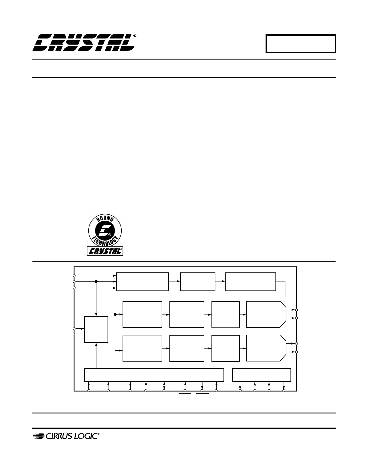
Description
The CS43122 is a complete high performance 24 bit192 kHz stereo digital-to-analog conversion system. The
device includes a digital interpolation filter followed by an
oversampled 5 bit delta-sigma modulator which drives
second generation dynamic-element-matching (DEM)
selection logic. The out put from the DEM block con trols
the input to a multi-element switched capacitor DAC/lowpass filter, with fully-differential outputs. This multi-bit architecture featur es significant ly lower out-of-band noise
and jitter sensitivity than traditional 1-bit designs, and the
advanced second generation DEM guarantees low noise
and distortion at all signal levels.
The CS43122 is the o ptimal D/A converter solution for
any application that requires the highest performance
and best possib le s oun d q ual ity i nclu ding high-end consumer and professional audio products such as
Universal DVD players, A/V receivers, Outboard D/A
Converters, CD Players, and Mixing Consoles.
ORDERING INFORMATION
CS43122-KS -10° to 70° C 28-pin SOIC
CDB43122 Evaluation Board
SCLK
LRCK
SDATA
MCLK
CLOCK
DIVIDER
M4
(AD0/CS)
M3 M2
(AD1/CDIN) (SCL/CCLK)
SERIAL INTERFACE
AND FORMAT SELECT
INTERPOLATION
INTERPOLATION
HARDWARE MODE CONTROL
Advance Product Information
P.O. Box 17847, Austin, Texas 78760
(512) 445 7222 FAX: (512) 445 7581
http://www.cirrus.com
DE-EMPHASIS
FILTER
SWITCHED
CAPACITOR-DAC
AND FILTER
SWITCHED
CAPACITOR-DAC
AND FILTER
VOLTAGE REFERENCE
FILT+
VREF CMOUTFILT-
FILTER
FILTER
(CONTROL PORT)
M1 M0
(SDA/CDOUT)
SOFT MUTE
MULTI-BIT
∆Σ
MODULATOR
MULTI-BIT
∆Σ
MODULATOR
RESET MUTEC MUTE
DYNAMIC
ELEMENT
MATCHING
LOGIC
DYNAMIC
ELEMENT
MATCHING
LOGIC
This document contains information for a new product.
Cirrus Logic reserves the right to modify this product without notice.
Copyright Cirrus Logic, Inc. 2000
(All Rights Reserved)
AOUTL+
AOUTL-
AOUTR+
AOUTR-
DEC ‘00
DS526PP2
1
Page 2

TABLE OF CONTENTS
1. CHARACTERISTICS/SPECIFICATIONS .................................................................................4
ANALOG CHARACTERISTICS................................................................................................ 4
DIGITAL CHARACTERISTICS................................................................................................. 8
ABSOLUTE MAXIMUM RATINGS ...........................................................................................8
RECOMMENDED OPERATING CONDITIONS.......................................................................8
SWITCHING CHARACTERISTICS . ...... ....... ...... ....... ...... ....................................... ...... ....... ..... 9
SWITCHING CHARACTERISTICS - CONTROL PORT.........................................................10
2. TYPICAL CONNECTION DIAGRAM ...................................................................................... 12
3. REGISTER DESCRIPTION .................................................................................................... 13
3.1 Mode Control Register (Address 01H)..............................................................................13
4. PIN DESCRIPTION ................................ ....... ...................................... ....... ...... ....... ...... .... ... ... 15
5. APPLICATIONS ......................................................................................................................19
5.1 Recommended Power-up Sequence ............................................................................... 19
6. CONTROL PORT INTERFACE .................................................................................... ....... ... 19
6.1 SPI Mode ......................................................................................................................... 19
6.2 2 Wire Mode ..................................................................................................................... 19
6.3 Memory Address Pointer (MAP) ..................................................................................... 20
7. PARAMETER DEFINITIONS ..................................................................................................25
8. REFERENCES ........................................................................................................................25
9. PACKAGE DIMENSIONS ....................................................................................................... 26
CS43122
Contacting Cirrus Logic Support
For a complete listing of Direct Sales, Distributor, and Sales Representative contacts, visit the Cirrus Logic web site at:
http://www.cirrus.com/corporate/contacts/sales.cfm
Preliminary product inf o rmation describes products whi ch are i n production, but for whi ch f ul l characterization data is not yet available. Advance product information describes products which are in development and subject to development changes. Cirrus Logic, Inc. has made best efforts to ensure that the information
contained in this document i s accurat e and reli able. However , t he infor mation is subje ct to chang e without noti ce and is provi d ed “AS IS” without warrant y of
any kind (express or implied). Customers are advised to obtain the latest version of relevant information to verify, before placing orders, that information being
relied on is current and complete. All products are sold subject to the terms and conditions of sale supplied at the time of order acknowledgment, including those
pertaining to warran t y , pa tent infringement, an d limitation of liability. No re s p onsibility is assumed b y Cirrus Logic, Inc. for the use of this informa tion, including
use of this inf orma t i on as the basis for manufacture or sale o f a ny i t e ms, nor for infrin gements of patents or other rights of third parties. This document i s the
property of Cirrus Logic, Inc. a nd by furni shing th is i nformati on, Cir rus L ogic, In c. grant s no l icense, express or i mpli ed under any patent s, mask work righ ts,
copyrights, trademarks, trad e secrets o r ot her i ntellect ual pro pert y right s of Cirrus L ogic, I nc. Ci rrus L ogic, In c., cop yright owner of the in forma tion co ntaine d
herein, gives consent for copies to be made of the information only for use within your organization with respect to Cirrus Logic integrated circuits or other parts
of Cirrus Logic, Inc. The same consent is gi ven for simi lar inf ormat ion con tai ned on a ny Cirru s Logic we bsite or disk. T his consent does not extend to othe r
copying such as copying for general distribution, advertising or promotional purposes, or for creating any work for resale. The names of products of Cirrus Logic,
Inc. or other vendors and suppliers appearing in this document may be trademarks or service marks of their respective owners which may be registered in some
jurisdictions. A list of Cirrus Logic, Inc. trademarks and service marks can be found at http://www.cirrus.com
.
2
Page 3

LIST OF FIGURES
Figure 1. Serial Audio Input Timing................................................................................................. 9
Figure 2. 2 Wire Mode Control Port Timing................................................................................... 10
Figure 3. SPI Control Port Timing ................ ....... ...................................... ....... ...... ....... ...... ..........11
Figure 4. Typical Connection Diagram...................... ....... ...... ...... ....... ...... ....... ............................. 1 2
Figure 5. Control Port Timing, SPI mode ...................................................................................... 20
Figure 6. Control Port Timing, 2 wire Mode................................................................................... 20
Figure 7. Operational Mode 0 Transition Band ............................................................................ 22
Figure 8. Operational Mode 0 Stopband Rejection ......................................................................22
Figure 9. Operational Mode 0 Transition Band ............................................................................ 22
Figure 10. Operational Mode 0 Frequency Response .................................................................22
Figure 11. Operational Mode 0 Stopband .....................................................................................22
Figure 12. Operational Mode 0 Transition Band ..........................................................................22
Figure 13. Operational Mode 0 Transition Band ..........................................................................22
Figure 14. Operational Mode 0 Frequency Response .................................................................22
Figure 15. Operational Mode 2 Stopband Rejection....................................................................23
Figure 16. Operational Mode 2 Transition Band ..........................................................................23
Figure 17. Operational Mode 2 Transition Band ..........................................................................23
Figure 18. Operational Mode 2 Frequency Response .................................................................23
Figure 19. De-Emphasis Curve.....................................................................................................23
Figure 20. Format 0, Left Justified................................................................................................24
Figure 21. Format 1, I
Figure 22. Format 2, Right Justified, 16-Bit Data .........................................................................24
Figure 23. Format 3, Right Justified, 24-Bit Data ..........................................................................24
CS43122
2
S..............................................................................................................24
LIST OF TABLES
Table 1. Operational Mode 0 (16 to 55 kHz sample rates) Common Clock Frequencies ................16
Table 2. Operational Mode 1 (45 to 105 kHz sample rates) Common Clock Frequencies .............16
Table 3. Operational Mode 2 (95 to 200 kHz sample rates) Common Clock Frequencies .............16
Table 4. Operational Mode 0 (16 to 55 kHz) Digital Interface Format Options................................. 21
Table 5. Operational Mode 0 (16 to 55 kHz) De-Emphasis Options ................................................ 21
Table 6. Operational Mode 1 (45 to 105 kHz) Sample Rate Mode Options .....................................21
Table 7. Operational Mode 2 (95 to 200 kHz) Sample Rate Mode Options .....................................21
3
Page 4
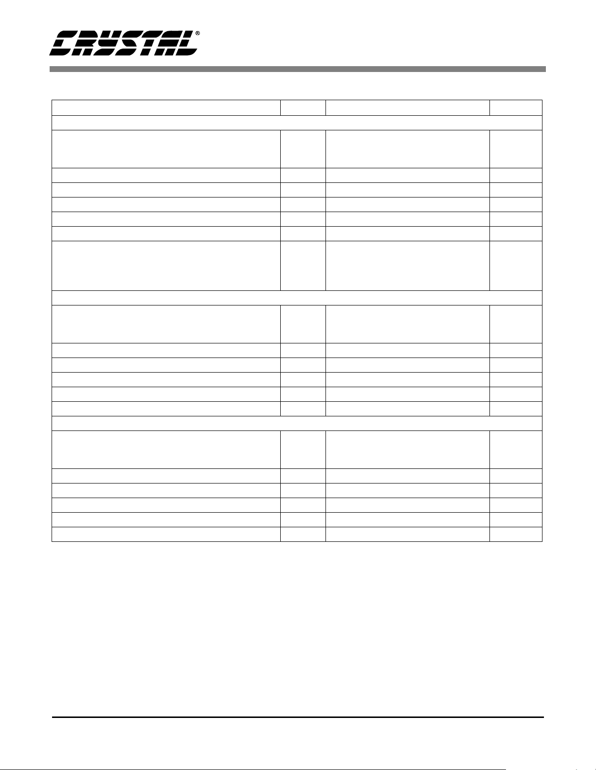
1. CHARACTERISTICS/SPECIFICATIONS
CS43122
ANALOG CHARACTERISTICS (T
= DGND;Full-Scale Output Sine Wave, 997 Hz; MCLK = 12.288 MHz; SCLK = 3.072 MHz; Measurement Bandwidth 10 Hz to 20 kHz, unless otherwise specified. Test load = R
Parameter Symbol Min Typ Max Unit
= 25° C; Logic "1" = VD = 3 V; VA = 5.5 V;VREF=5.5 V Logic "0"
A
= 1kΩ, CL = 10 pF)
L
Dynamic Performance - Operational Mode 1 (Fs = 48 kHz)
Dynamic Range (Note 1)
24-Bit unweighted
A-Weighted
16-Bit unweighted
(Note 2) A-Weighted
Total Harmonic Distortion + Noise (Note 1)
24-Bit 0 dB
-20 dB
-60 dB
16-Bit 0 dB
(Note 2) -20 dB
-60 dB
THD+N
TBD
TBD
-
-
-
-
-
-
-
-
119
122
95
98
-102
-99
-59
-95
-75
-35
-
-
-
-
TBD
TBD
TBD
-
-
-
dB
dB
dB
dB
dB
dB
dB
dB
dB
dB
4
Page 5
ANALOG CHARACTERISTICS (CONTINUED)
Parameter Symbol Min T yp Max Unit
Dynamic Performance - Operational Mode 0 (Fs = 48 kHz)
Dynamic Range (Note 1)
24-Bit unweighted
A-Weighted
16-Bit unweighted
(Note 2) A-Weighted
Total Harmonic Distortion + Noise (Note 1)
24-Bit 0 dB
-20 dB
-60 dB
16-Bit 0 dB
(Note 2) -20 dB
-60 dB
Dynamic Performance - Operational Mode 1 (Fs = 96 kHz)
Dynamic Range (Note 1)
24-Bit unweighted
A-Weighted
40 kHz bandwidth
unweighted
16-Bit unweighted
(Note 2) A-Weighted
Total Harmonic Distortion + Noise (Note 1)
24-Bit 0 dB
-20 dB
-60 dB
16-Bit 0 dB
(Note 2) -20 dB
-60 dB
Dynamic Performance - Operational Mode 2 (Fs = 192 kHz)
Dynamic Range (Note 1)
24-Bit unweighted
A-Weighted
40 kHz bandwidth
unweighted
16-Bit unweighted
(Note 2) A-Weighted
Total Harmonic Distortion + Noise (Note 1)
24-Bit 0 dB
-20 dB
-60 dB
16-Bit 0 dB
(Note 2) -20 dB
-60 dB
THD+N
THD+N
THD+N
TBD
TBD
-
-
-
-
-
-
-
-
TBD
TBD
TBD
-
-
-
-
-
-
-
-
TBD
TBD
TBD
-
-
-
-
-
-
-
-
117
120
95
98
-100
-97
-55
-95
-75
-35
117
120
114
92
98
-100
-97
-55
-95
-75
-35
117
120
114
95
98
-100
-97
-55
-95
-75
-35
CS43122
-
-
-
-
TBD
TBD
TBD
-
-
-
-
-
-
-
-
TBD
TBD
TBD
-
-
-
-
-
-
-
-
TBD
TBD
TBD
-
-
-
dB
dB
dB
dB
dB
dB
dB
dB
dB
dB
dB
dB
dB
dB
dB
dB
dB
dB
dB
dB
dB
dB
dB
dB
dB
dB
dB
dB
dB
dB
dB
dB
5
Page 6
CS43122
ANALOG CHARACTERISTICS (CONTINUED)
Parameter Symbol VD = 3 V VD = 5 V Unit
Power Supplies
Supply Current normal operation
VA = 5 .0V normal operation
power-down state
I
I
ID + I
Power Dissipation normal operation
VA = 5 .0V power-down
Power Supply Rejection Ratio (1 kHz) (Note 3)
PSRR -
(120 Hz)
Parameter Symbol Min Typ Max Unit
Analog Output
Full Scale Differential Output Voltage TBD 1.33VREF TBD Vpp
Common Mode Voltage - 0.5VREF - VDC
Interchannel Gain Mismatch - 0.1 - dB
Gain Drift - 100 - ppm/°C
Differential DC Offset - 2.0 TBD mV
AC-Load Resistance R
Load Capacitance C
Interchannel Isolation (1 kHz) - 90 - dB
Min Typ Max Min Typ Max
-
17
A
D
-
-
A
-
-
-
L
L
1.0 - - kΩ
--100pF
27
60
166
0.3
60
40
TBD -
TBD--
-
-
-
-
-
-
-
17
24
30
205
0.3
60
40
TBD
mA
mA
-
µA
TBD-mW
mW
-
-
dB
dB
Notes: 1. Triangular PDF dithered data.
2. Performance limite d b y 16 -bi t qu an ti zation noise.
3. Valid with the recommended capacitor values on FILT+ and CMOUT as shown in Figure 1. Increasing
the capacitance will also increase the PSRR.
6
Page 7
CS43122
ANALOG CHARACTERISTICS (Continued)
Parameter Symbol Min Typ Max Unit
Combined Digital and On-chip Analog Filter Response - Operational Mode 0
Passband (Note 4)
to -0.1 dB corner
to -3 dB corner
Frequency Response 10 Hz to 20 kHz -.020 - +0.015 dB
Passband Ripple - - ±0.0001 dB
StopBand .5465 - - Fs
StopBand Attenuation (Note 5) 102 - - dB
Group Delay (Note 6) tgd - 37/Fs - s
De-emphasis Error (Note 7)
Fs = 32 kHz
(Relative to 1 kHz) Fs = 44.1 kHz
Fs = 48 kHz
Combined Digital and On-chip Analog Filter Response - Operational Mode 1
Passband (Note 4)
to -0.1 dB corner
to -3 dB corner
Frequency Response 10 Hz to 20 kHz -0.017 - 0.035 dB
Passband Ripple - - ±0.0008 dB
StopBand .570 - - Fs
StopBand Attenuation (Note 5) 82 - - dB
Group Delay tgd - 20/Fs - s
Combined Digital and On-chip Analog Filter Response - Operational Mode 2
Passband (Note 4)
to -0.1 dB corner
to -3 dB corner
Frequency Response 10 Hz to 20 kHz 0 - +0.015 dB
Passband Ripple - - ±0.00065 dB
StopBand 0.635 - - Fs
StopBand Attenuation (Note 5) 83 - - dB
Group Delay tgd - 11/Fs - s
-
-
-
-
-
0
0
-
-
-
-
-
-
-
-
-
-
-
0.470
0.492
±0.10
±0.10
±0.13
0.448
0.486
0.385
0.472
dB
dB
dB
Fs
Fs
Fs
Fs
Fs
Fs
Notes: 4. Response is clock dependent and will scale with Fs. Note that the response plots (Figures 7-18) have
been normalized to Fs and can be de-normalized by multiplying the X-axis scale by Fs.
5. For Operational Mode 0, the Measurement Bandwidth is 0.5465 Fs to 1.4 Fs.
For Operational Mode 1, the Measurement Bandwidth is 0.570 Fs to 1.4 Fs.
For Operational Mode 2, the Measurement Bandwidth is 0.635 Fs to 1.3 Fs.
6. Group Delay for Fs=48 kHz 37/48 kHz=770 µs
7. De-em pha si s is availab le onl y in Op er ati ona l Mode 0.
7
Page 8

CS43122
DIGITAL CHARACTERISTICS (T
= 25° C; VD = 3.0 V - 5.25 V)
A
Parameters Symbol Min Typ Max Units
High-Level Input Voltage VD = 5 V
VD = 3 V
Low-Level Input Voltage VD = 5 V
VD = 3 V
Input Leakage Current I
V
IH
2.0
2.0
V
IL
-
-
in
--±10µA
-
-
-
-
-
-
0.8
0.8
V
V
V
V
Input Capacitance - 8 - pF
Maximum MUTEC Drive Current - 3 - mA
ABSOLUTE MAXIMUM RATINGS (AGND = 0 V, all voltages with respect to ground.)
Parameter Symbol Min Max Unit
DC Power Supply: Positive Analog
Positive Digital
Reference Voltage
Input Current, Any Pin Except Supplies I
Digital Input Voltage V
Ambient Operating Temperature (power applied) T
Storage Temperature T
WARNING: WARNING:Operation at or beyond these limits may result in permanent damage to the device. Normal
operation is not guaranteed at these extremes.
VA
VD
VREF
in
IND
A
stg
-0.3
-0.3
-0.3
6.0
6.0
VA
V
V
V
-±10mA
-0.3 (VD)+0.4 V
-55 125 °C
-65 150 °C
RECOMMENDED OPERATING CONDITIONS
Parameter Symbol Min Typ Max Unit
DC Power Supply: Positive Digital
Positive Analog
Reference Voltage
Specified Temperature Range T
VD
VA
VREF
(DGND = 0V; all voltages with respect to ground)
3.0
5.25
5.25
A
-10 - 70 °C
3.3
5.5
5.5
5.25
5.75
VA
V
V
V
8
Page 9
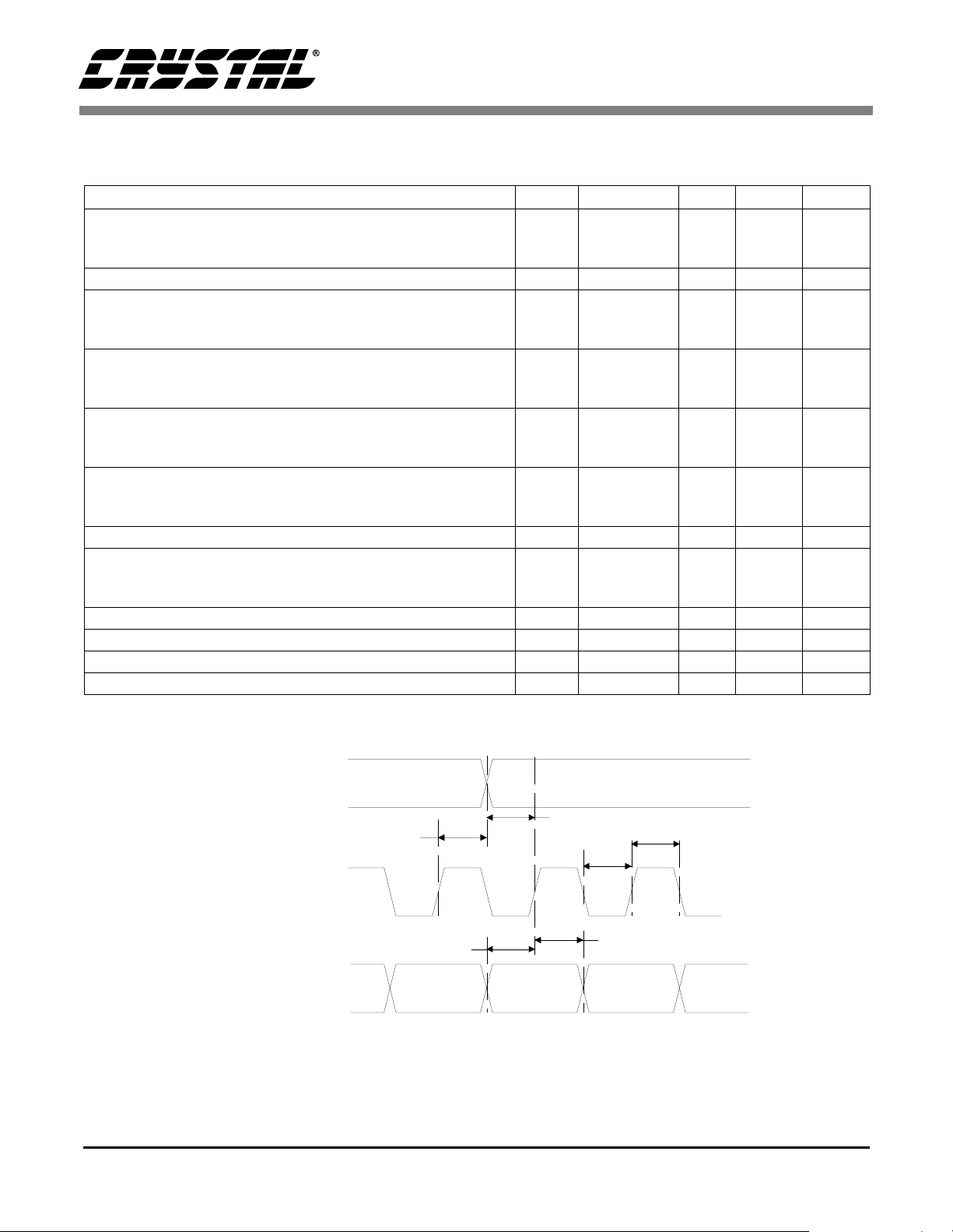
CS43122
SWITCHING CHARACTERISTICS (T
1 = VD = 5.25 to 3.0 Volts; C
=20pF)
L
= -10 to 70° C; Logic 0 = AGND = DGND; Logic
A
Parameter Symbol Min Typ Max Unit
Input Sample Rate (Operational Mode 0)
(Operational Mode 1)
(Operational Mode 2)
Fs
Fs
Fs
16
45
95
-
-
-
55
105
200
kHz
kHz
kHz
LRCK Duty Cycle 45 50 55 %
MCLK Frequency (Operational Mode 0, 256 Fs)
(Operational Mode 1, 128 Fs)
4.096
- 14.08 MHz
(Operational Mode 2, 64 Fs)
MCLK Frequency (Operational Mode 0, 384 Fs)
(Operational Mode 1, 192 Fs)
6.144
- 21.12 MHz
(Operational Mode 2, 96 Fs)
MCLK Frequency (Operational Mode 0, 512 Fs)
(Operational Mode 1, 256 Fs)
8.192
- 28.16 MHz
(Operational Mode 2 , 128 Fs)
MCLK Frequency (Operational Mode 0, 768 Fs)
(Operational Mode 1, 384 Fs)
12.288
- 42.24 MHz
(Operational Mode 2 , 192 Fs)
MCLK Duty Cycle 40 50 60 %
SCLK Frequency (Operational
Mode 0) (Operational Mode 1)
(Operational Mode 2)
SCLK rising to LRCK edge delay t
SCLK rising to LRCK edge setup time t
SDATA valid to SCLK rising setup time t
SCLK rising to SDATA hold time t
slrd
slrs
sdlrs
sdh
-
-
-
-
-
-
256×Fs
128×Fs
64×Fs
20 - - ns
20 - - ns
20 - - ns
20 - - ns
Hz
Hz
Hz
LRCK
SCLK
SDATA
t
t
slrd
t
sdlrs
slrs
t
sclkl
Figure 1. Serial Audio Input Timing
t
sdh
t
sclkh
9
Page 10
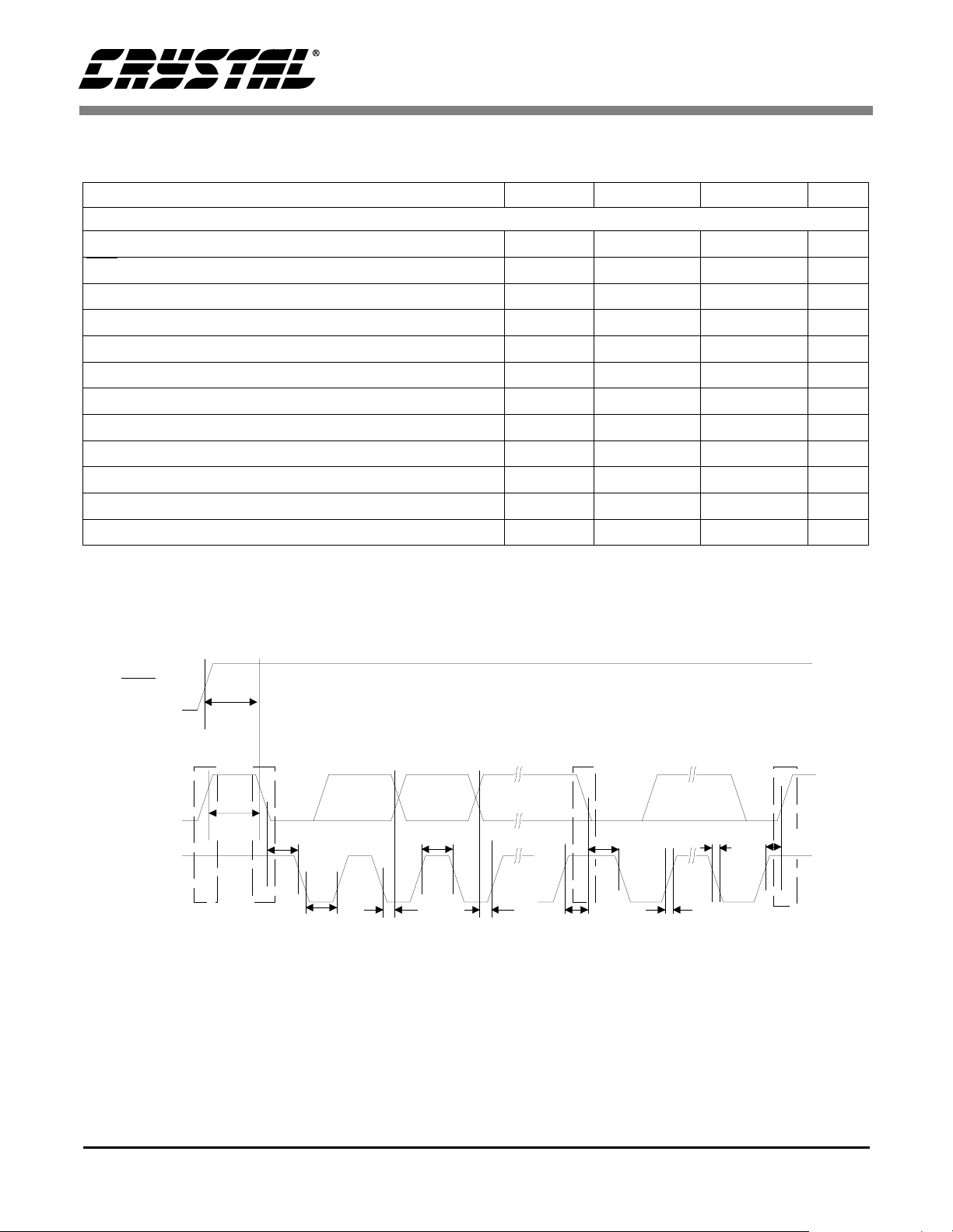
SWITCHING CHARACTERISTICS - CONTROL PORT
(TA = 25° C; VD = 5.25 V to 3.0 Volts; Inputs: logic 0 = AGND, logic 1 = VD, CL = 30 pF)
Parameter Symbol Min Max Unit
2 Wire Mode
SCL Clock Frequency f
Rising Edge to Start t
RST
Bus Free Time Between Transmissions t
Start Condition Hold Time (prior to first clock pulse) t
Clock Low time t
Clock High Time t
Setup Time for Repeated Start Condition t
SDA Hold Time from SCL Falling (Note 8) t
SDA Setup time to SCL Rising t
Rise Time of Both SDA and SCL Lines t
Fall Time of Both SDA and SCL Lines t
Setup Time for Stop Condition t
scl
irs
buf
hdst
low
high
sust
hdd
sud
r
f
susp
-100KHz
500 - ns
4.7 - µs
4.0 - µs
4.7 - µs
4.0 - µs
4.7 - µs
0-µs
250 - ns
-1µs
-300ns
4.7 - µs
CS43122
Notes: 8. Data must be held for sufficient time to bridge the 300 ns transition time of SCL.
RST
t
SDA
SCL
irs
Stop Start
t
buf
t
t
hdst
low
t
hdd
t
high
t
sud
Repeated
Start
t
t
sust
hdst
t
f
t
r
Figure 2. 2 Wire Mode Control Port Timing
Stop
t
susp
10
Page 11
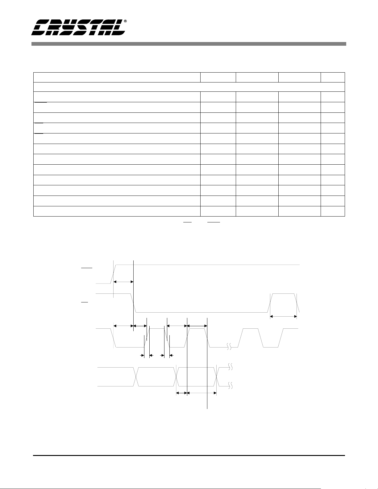
SWITCHING CHARACTERISTICS - CONTROL PORT
(TA = 25° C; VD = 5.25 V to 3.0 Volts; Inputs: logic 0 = AGND, logic 1 = VD, CL = 30 pF)
Parameter Symbol Min Max Unit
SPI Mode
CCLK Clock Frequency f
Rising Edge to CS Falling t
RST
CCLK Edge to CS
High Time Between Transmissions t
CS
Falling to CCLK Edge t
CS
CCLK Low Time t
CCLK High Time t
CDIN to CCLK Rising Setup Time t
CCLK Rising to DATA Hold Time (Note 10) t
Rise Time of CCLK and CDIN (Note 11) t
Fall Time of CCLK and CDIN (Note 11) t
CCLK Falling to CDOUT valid t
Falling (Note 9) t
sclk
srs
spi
csh
css
scl
sch
dsu
dh
r2
f2
ov
-6MHz
500 - ns
500 - ns
1.0 - µs
20 - ns
66 - ns
66 - ns
40 - ns
15 - ns
-100ns
-100ns
45 ns
CS43122
Notes: 9. t
10. Data must be held for sufficient time to bridge the transition time of CCLK.
11. For F
only needed before first falling edge of CS after RST rising edge. t
spi
< 1 MHz
SCK
RST
t
srs
CS
t
t
spi
css
t
scl
t
sch
CCLK
t
r2
t
f2
CDIN
t
dsu
t
dh
= 0 at all other times.
spi
t
csh
Figure 3. SPI Control Port Timing
11
Page 12

2. TYPICAL CONNECTION DIAGRAM
CS43122
3.3 - 5.0 V
Processor
Mode
Select
Audio
Data
+
10 µf
0.1µF
5
14
4
3
2
12
11
13
15
7
VD
M0
M1
M2
M3
M4
LRCK
SCLK
SDATA
MUTE
8
VD
CS43122
22
VA
VREF
FILT+
FILT-
AOUTL-
AOUTL+
MUTEC
AOUTR-
28
27
26
24
23
17
19
0.1 µf
+
.01 µf
+
0.1 µf 100 µf
Analog
Conditioning
Analog
Conditioning
10
µf
+5.5V
100 µf
+
+
+5.5V
12
External Clock
1
RST
10
MCLK
16
C/H
DGND
6
Figure 4. Typical Connection Diagram
AOUTR+
CMOUT
AGND
21
189
20
25
.01 µf 10 µf
+
Page 13

CS43122
3. REGISTER DESCRIPTION
3.1 MODE CONTROL REGISTER (ADDRESS 01H)
76543210
CAL MUTE
00
4.11 Differential DC offset calibration (CAL)
Default = 0
0 - Disabled
1 - Enabled
Function:
Enabling this function will initiate a calibration to minimize the differential DC offset. This function will
be automatically reset following completion of the calibration sequence.
4.12 Soft Mute (MUTE)
Default = 0
0 - Disabled
1 - Enabled
M4 M3 M2 M1 M0 PDN
000000
Function:
The analog outputs will ramp to a muted state when enabled. The ramp requires 1152 left/right clock
cycles in Operational Mode 0, 2304 cycles in Operational Mode 1 and 4608 cycles in Operational
Mode 2 . The bias voltage on the outputs will be retained and MUTEC
of the ramp period.
The analog outputs will ramp to a normal state when this function transitions from the enabled to disabled state. The ramp requires 1152 left/right clock cycles in Operational Mode 0, 2304 cycles in Operational Mode 1 and 4608 cycles in Operational Mode 2 . The MUTEC
disabling of MUTE
4.13 Mode Select (M4-M0)
.
will go low at the completion
will go high immediately on
Default = 00000
Function:
The Mode Select pins determine the operational mode of the device as detailed in T ables 4-7. The options
include:
Selection of the Digital Interface Format which determines the required relationship between the
Left/Right clock, serial clock and serial data as detailed in Figures 20-23
Selection of the standard 15 µs/50 µs digital de-emphasis filter response, Figure 28, which requires reconfiguration of the digital filter to maintain the proper filter response for 32, 44.1 or 48 kHz sample rates.
Selection of the appropriate operational clocking mode to match the input sample rates.
13
Page 14

CS43122
4.14 Power Down (PDN)
Default = 1
0 - Disabled
1 - Enabled
Function:
The analog and digital sections will be placed into a power-down mode when this function is enabled.
This bit must be cleared to resume normal operation.
14
Page 15
4. PIN DESCRIPTION
CS43122
Reset RST
See Description M4(AD0/CS
See Description M 3(AD1/CDIN) FILT- Reference Ground
See Description M2(SCL/CCLK) CMOUT Common ModeS Voltage
See Description M0(SDA/CDOUT) AOUTL- Differential Output
Digital Ground DGND AOUTL+ Differential Output
Digital Power VD VA Analog Power
Digital Power VD AGND Analog Ground
Digital Ground DGND AOUTR+ Differential Output
Master Clock MCLK AOUTR- Differential Output
Serial Clock SCLK AGND Analog Ground
Left/Right Clock LRCK MUTEC
Serial Data SDATA C/H
See Description M1 MUTE
RST
DGND
VD
1
6, 9
7, 8
Reset (
registers are reset when low. When high, the device will be in a normal operation
mode.
Digital Ground (
Digital Power (
Input
1
1
) FILT+ Reference Filter
2
2
3
4
5
5
6
6
7
8
9
10
11
12
13
14
) - The device enters a low power mode and all internal state machines
Input
Input
28
27
26
25
24
23
22
21
20
19
18
17
16
15
) - Digital ground reference.
) - Digital power supply. Typically 3.0 to 5.0 VDC.
VREF Voltage Reference
Mute Control
Control port/Hardware select
Soft Mute
15
Page 16

CS43122
MCLK
10
Master Clock (
512x or 768x the input sample rate in Operational Mode 0; either 128x, 192x 256x
or 384x the input sample rate in Operational Mode 1 ; or 64x, 96x 128x or 192x the
input sample rate in Operational Mode 2 . Tables 4-6 illustrate the standard audio
sample rates and the required master clock frequencies.
Sample Rate
(kHz)
32 8.1920 12.2880 16.3840 24.5760
44.1 11.2896 16.9344 22.5792 33.8688
48 12.2880 18.4320 24.5760 36.8640
Table 1. Operational Mode 0 (16 to 55 kHz sample rates ) C ommon Clock
Sample Rate
(kHz)
48 6.1440 8.1920 12.2880 16.3840
64 8.1920 12.2880 16.3840 24.5760
88.2 11.2896 16.9344 22.5792 33.8688
96 12.2880 18.4320 24.5760 36.8640
Table 2. Operational Mode 1 (45 to 105 kHz sample rates) Common Clock
Sample Rate
(kHz)
176.4 11.2896 16.9344 22.5792 33.8688
192 12.2880 18.4320 24.5760 36.8640
Table 3. Operational Mode 2 (95 to 200 kHz sample rates) Common Clock
Input
) - The master clock frequency must be either 256x, 384x,
MCLK (MHz)
256x 384x 512x 768x
Frequencies
MCLK (MHz)
128x 192x 256x 384x
Frequencies
MCLK (MHz)
64x 96x 128x 192x
Frequencies
SCLK
LRCK
SDATA
16
11
12
13
Serial Clock
required relationship between the Left/Right clock, serial clock and serial data is
defined by either the Mode Control Byte in Control Port Mode or the M0 - M4 pins
in Hardware Mode. The options are detailed in Figures 20-23.
Left/Right Clock
rently being input on the serial audio data input, SDATA. The frequency of the
Left/Right clock must be at the input sample rate. Audio samples in Left/Right
sample pairs will be simultaneously output from the digital-to-analog converter
whereas Right/Left pairs will exhibit a one sample period difference. The required
relationship between the Left/Right clock, serial clock and serial data is defined by
the Mode Control Byte and the options are detailed in Figures 20-23.
Serial Audio Data
this pin. The data is clocked into SDATA via the serial clock and the channel is
determined by the Left/Right clock. The required relationship between the
Left/Right clock, serial clock and serial data is defined by the Mode Control Byte
and the options are detailed inin Figures 20-23.
(Input) -
(Input) -
(Input) -
Clocks individual bits of serial data into the SDATA pin. The
The Left/Right clock determines which channel is cur-
Two’s complement MSB-first serial data is input on
Page 17

CS43122
MUTE
C/H
MUTEC
AGND
AOUTR- , AOUTR+
AOUTL- , AOUTL+
VA
CMOUT
FILT-
FILT+
VREF
M0, M1, M2, M3, M4
(Hardware Mode)
AD0 / CS
(Control Port Mode)
15
16
17
18, 21
19, 20,
23, 24
22
25
26
27
28
2, 3, 4,
5,14
2
Soft Mute
(Input) -
The analog outputs will ramp to a muted state when enabled.
The ramp requires 1152 left/right clock cycles in Operational Mode 0, 2304 cycles
in Operational Mode 1 and 4608 cycles in Operational Mode 2 . The bias voltage
on the outputs will be retained and MUTEC
will go active at the completion of the
ramp period.
The analog outputs will ramp to a normal state when this function transitions from
the enabled to disabled state. The ramp requires 1152 left/right clock cycles in
Operational Mode 0, 2304 cycles in Operational Mode 1 and 4608 cycles in Operational Mode 2 . The MUTEC
will release immediately on setting MUTE = 1.
The converter analog outputs will mute when enabled. The bias voltage on the
outputs will be retained and MUTEC
Control Port / Hardware Mode Select
will go active during the mute period
(Input) -
Determines if the device will oper-
ate in either the Hardware Mode or Control Port Mode.
Mute Control
(Output)
- The
Mute Control pin goes low during power-up initialization, reset, muting, maste r clock to left/right clock frequency ratio is incorrect or
power-down. T his pin is inte nded to be use d as a contro l for a n extern al m ute circ uit
to prevent the clicks and pops that can occur in any single supply system. Use of
Mute Control is not mandatory but recommended for designs requiring the absolute
minimum in extraneous clicks
Analog Ground
(Inputs) -
Differential Analog Outputs
and pops.
Analog ground reference.
(Outputs)
- The full scale differential analog output
level is specified in the Analog Characteristics specifications table.
Analog Power
(Input)
- Power for the analog and reference circuits. Typically
5.5 V DC.
Common Mode Voltage
(Output)
- Filter connection for internal bias voltage, typically 50% of VREF. Capacitors must be connected from CMOUT to analog
ground, as shown in the Typical Connection Diagram. CMOUT has a typical
source impedence of 25 kΩ and any current drawn from this pin will alter device
performance.
Reference Ground
(Input) -
Ground reference for the internal sampling circuits.
Must be connected to analog ground.
Referenc e Fi l t er
(Output)
- Positive reference for internal sampling circuits. External capacitors are required from FILT+ to analog ground, as shown in the Typical
Connection Diagram. The recommended values will typically provide 60 dB of
PSRR at 1 kHz and 40 dB of PSRR at 120 Hz. FILT+ is not intended to supply
external current.
Voltage Reference Input
Mode Select
(Inputs) -
(Input) -
Analog voltage reference. Typically 5.5 VDC.
The Mode Select pins determine the operational mode of
the device as detailed in Tables 4-7. The options include;
Selection of the Digital Interface Format which determines the required relationship between the Left/Right clock, serial clock and serial data as detailed in Figures 20-23Selection of the standard 15 µs/50 µs digital de-emphasis filter
response, Figure 28, which requires reconfiguration of the digital filter to maintain
the proper filter response for 32, 44.1 or 48 kHz sample rates.
Selection of the appropriate clocking mode to match the input sample rates.
Address Bit 0 / Chip Select
is used to enable the control port interface in SPI mode. The device will enter
CS
(Input) -
In 2 wire mode, AD0 is a chip address bit.
the SPI mode at anytime a high to low transition is detected on this pin. Once the
device has entered the SPI mode, it will remain until either the part is reset or
undergoes a power-down cycle.
17
Page 18

CS43122
AD1/CDIN
(Control Port Mode)
SCL/CCLK
(Control Port Mode)
SDA/CDOUT
(Control Port Mode)
M1
(Control Port Mode)
14
3
Address Bit 1 / Control Data Input
(Input) -
In 2 Wire Mode, AD1 is a chip
address bit. CDIN is the control data input line for the control port interface in SPI
mode.
4
Serial Control Interface Clock
(Input) -
In 2 Wire Mode, SCL clocks the serial
control data into or from SDA/CDOUT.
In SPI mode, CCLK clocks the serial data into AD1/CDIN and out of SDA/CDOUT.
5
Serial Control Data I/O
(Input/Output) -
In 2 Wire Mode, SDA is a data input/out-
put. CDOUT is the control data output for the control port interface in SPI mode.
Mode Select
(Input) -
This pin is not used in Control Port Mode and must be termi-
nated to ground.
18
Page 19

CS43122
5. APPLICATIONS
5.1 Recommended Power-up Sequence
1) Hold RST high until the power supplies, master
clock, and left/right clock are stable.
2) Bring RST high.
6. CONTROL PORT INTERFACE
The control port is used to load all the internal settings of the CS43122. The operation of the control
port may be completely asynchronous to the audio
sample rate. However, to avoid potential interference problems, the control port pins should remain
static if no operation is required.
The control port has 2 modes: SPI and “2 wire”,
with the CS43122 operating as a slave device in
both modes. If 2 wire operation is desired, AD0/CS
should be tied to VD or DGND. If the CS43122
ever detects a high to low transition on AD0/CS after power-up, SPI mode will be selected.
6.1 SPI Mode
next 8 bits are the data which will be plac ed into the
register designated by the MAP.
6.2 2 Wire Mode
In 2 Wire Mode, SDA is a bi-directional data line.
Data is clocked into and out of the part by the clock,
SCL, with the clock to data relationship as shown
in Figure 2. There is no CS pin. Pins AD0 and AD1
form the partial chip address and should be tied to
VD or DGND as required. The 7-bit addres s field,
which is the first byte sent to the CS43122, m ust be
00100(AD1)(AD0) where (AD1) and (AD0) match
the setting of the AD0 and AD1 pins. The eighth bit
of the address byte is the R/W bit (high for a read,
low for a write). If the operation is a write, the next
byte is the Memory Address Pointer, MAP, which
selects the register to be read or written. The MAP
is then followed by the data to be written. If the operation is a read, then the contents of the register
pointed to by the MAP will be output after the chip
address.
In SPI mode, CS is the CS43122 chip select signal,
CCLK is the control port bit cl ock, C DIN i s the input data line from the microcontroller, CDOUT is
the data output and the chip address is 0010000.
The data is clocked on the rising edge of CCLK.
Figure 5 shows the operation of the control port in
SPI mode. To write to a register, bring CS low. The
first 7 bits on CDIN form the chip address, and
must be 0010000. The eighth bit is a read/write indicator (R/W). The next 8 bits form the Memory
Address Pointer (MAP), which is set to 01h. The
19
Page 20

CS43122
6.3 Memory Address Pointer (MAP)
76543210
INCR Reserved Reserved Reserved Reserved MAP2 MAP1 MAP0
00000001
INCR (Auto MAP Increment Enable) MAP0-2 (Memory Address Pointer)
Default = ‘0’ Default = ‘001’
0 - Disabled
1 - Enabled
SDA
SCL
RST
CS
CCLK
CDIN
001000
t
srs
t
t
css
spi
tr2t
t
t
sch
scl
f2
t
t
dsu
dh
Figure 5. Control Port Timing, SPI mode
Note 1
ADDR
AD0
R/W
ACK
DATA
1-8
ACK
t
csh
DATA
1-8
ACK
20
Start
Stop
Note: If operation is a write, t his byte contains the Memory Address Pointer, MAP.
Figure 6. Control Port Timing, 2 wire Mode
Page 21

CS43122
M4 M1
(DIF1)
M0
(DIF0)
DESCRIPTION FORMAT FIGURE
0 0 0 Left Justified, up to 24-bit data 0 20
00 1
2
S, up to 24-bit data
I
121
0 1 0 Right Justified, 16-bit Data 2 22
0 1 1 Right Justified, 24-bit Data 3 23
Table 4. Operational Mode 0 (16 to 55kHz) Digital Interface Format Options
M4 M3
(DEM1)
M2
(DEM0)
DESCRIPTION FIGURE
0 0 0 32 kHz De-Emphasis 19
0 0 1 44.1 kHz De-Emphasis 19
0 1 0 48 kHz De-Emphasis 19
0 1 1 De-Emphasis Disabled -
Table 5. Operational Mode 0 (16 to 55kHz) De-Emphasis Options
M4 M3 M2 M1 M0 DESCRIPTION
11100Left Justified up to 24-bit data, Format 0
11101
2
S up to 24-bit data, Format 1
I
11110Right Justified 16-bit data, Format 2
11111Right Justified 24-bit data, Format 3
Table 6. Operational Mode 1 (45 to 105 kHz) Sample Rate Mode Options
M4 M3 M2 M1 M0 DESCRIPTION
11000Left Justified up to 24-bit data, Format 0
11001
2
I
S up to 24-bit data, Format 1
11010Right Justified 16-bit data, Format 2
11011Right Justified 24-bit data, Format 3
Table 7. Operational Mode 2 (95 to 200 kHz) Sample Rate Mode Options
21
Page 22

0
-20
-40
-60
-80
-100
Amplitude dB
-120
-140
-160
0.46 0.48 0.50 0.52 0.54 0.56 0.58 0.6
0.45 0.46 0.47 0.480.49 0.5 0.51 0.52 0.53 0.54 0.55 0.56 0.570.58 0.59 0.6
Frequency (normalized to Fs)
Figure 7. Operational Mode 0 Transition Band Figure 8. Operational Mode 0 Stopband Rejection
0
-20
-40
-60
-80
-100
Amplitude dB
-120
-140
-160
0.45 0.5 0.55 0.6 0.65 0.7 0.75 0.8 0.85 0.9 0.95 1
Freque ncy (normalized to Fs)
CS43122
0
-1
-2
-3
-4
-5
-6
Amplitude dB
-7
-8
-9
-10
0.45 0.46 0.47 0.48 0.49 0.5 0.51 0.52
Frequency (normal i zed to Fs)
0.1
0.08
0.06
0.04
0.02
0
-0.02
Amplitude dB
-0.04
-0.06
-0.08
-0.1
0 0.05 0.1 0.15 0.2 0.25 0.3 0.35 0.4 0.45
Frequency (normal i z ed to Fs)
Figure 9. Operational Mode 0 Transition Band Figure 10. Operational Mode 0 Frequency Response
0
-20
-40
-60
-80
Amplitude dB
-100
-120
-140
0.4 0.45 0.5 0.55 0.6 0.65 0.7 0.75 0.8 0.85 0.9 0.95 1
Freque ncy (normali z ed to Fs)
0
-20
-40
-60
-80
Amplitude dB
-100
-120
-140
0.4 0.45 0.5 0.55 0.6
Freque ncy (normali z ed to Fs)
Figure 11. Operational Mode 0 Stopband Figure 12. Operational Mode 0 Transition Band
0
-1
-2
-3
-4
-5
-6
Amplitude dB
-7
-8
-9
-10
0.42 0.43 0.44 0.45 0.46 0.47 0.48 0.49 0.5 0.51 0.52
Frequency (normal i zed to Fs)
0.1
0.08
0.06
0.04
0.02
0
-0.02
Amplitude dB
-0.04
-0.06
-0.08
-0.1
0 0.05 0.1 0.15 0.2 0.25 0.3 0.35 0.4 0.45
Frequency (normal i z ed to Fs)
Figure 13. Operational Mode 0 Transition Band Figure 14. Operational Mode 0 Frequency Response
22
Page 23

CS43122
0
-20
-40
-60
-80
-100
Amplitude dB
-120
-140
-160
0.4 0.45 0.5 0.55 0.6 0.65 0.7 0.75 0.8 0.85 0.9 0.95 1
Freque ncy (normali z ed to Fs)
0
-20
-40
-60
-80
-100
Amplitude dB
-120
-140
-160
0.5 0.52 0.54 0.56 0.58 0.6 0.62 0.64 0.66 0.68 0.7
Freque ncy (normali z ed to Fs)
Figure 15. Operational Mode 2 Stopband Rejection Figure 16. Operational Mode 2 Transition Band
0
-1
-2
-3
-4
-5
-6
Amplitude dB
-7
-8
-9
-10
0.35 0.37 0.39 0.41 0.43 0.45 0.47 0.49 0.51 0.53
Frequency (normal i zed to Fs)
0.1
0.08
0.06
0.04
0.02
0
-0.02
Amplitude dB
-0.04
-0.06
-0.08
-0.1
0 0.05 0.1 0.15 0.2 0.25 0.3 0.35 0.4
Frequency (normal i z ed to Fs)
Figure 17. Operational Mode 2 Transition Band Figure 18. Operational Mode 2 Frequency Response
Gain
dB
0dB
-10dB
T1=50 µs
F1 F2
3.183 kHz 10.61 kHz
Figure 19. De-Emphasis Curve
T2 = 15 µs
Frequency
23
Page 24

CS43122
LRCK
SCLK
SDATA +3 +2 +1
LRCK
SCLK
SDATA +3 +2 +1
MSB
-1 -2 -3 -4 -5
MSB
-1 -2 -3 -4 -5
Left Channel
+5 +4
Left Channel
+5 +4
LSB
MSB
-1 -2 -3 -4
Figure 20. Format 0, Left Justified
LSB
MSB
-1 -2 -3 -4
Figure 21. Format 1, I2S
Right Channel
+3 +2 +1
+5 +4
Right Channel
+3 +2 +1
+5 +4
LSB
LSB
LRCK
SCLK
SDATA
LRCK
SCLK
SDATA
Left Channel
15 14 13 12 11 10
32 clocks
6543210987
15 14 13 12 11 10
Right Channel
6543210987
Figure 22. Format 2, Right Justified, 16-Bit Data
Left Channel
0
23 22 21 20 19 18
32 clocks
65432107
23 22 21 20 19 18
Right Channel
65432107
Figure 23. Format 3, Right Justified, 24-Bit Data
24
Page 25

7. PARAMETER DEFINITIONS
Total Harmonic Distortion + Noise (THD+N)
The ratio of the rms value of the signal to the rms sum of all other spectral components over the specified
bandwidth (typically 10 Hz to 20 kHz), including distortion components. Expressed in decibels.
Dynamic Range
The ratio of the full scale rms value of the signal to the rms sum of all other spectral components over the
specified bandwidth. Dynamic range is a signal-to-noise measurement over the specified bandwidth
made with a -60 dBFS signal. 60 dB is then added to the resulting measurement to refer the measurement
to full scale. This technique ensures that the distortion components are below the noise level and do not
effect the measurement. This measurement technique has been accepted by the Audio Engineering Society, AES17-1991, and the Electronic Industries Association of Japan, EIAJ CP-307.
Interchannel Isolation
A measure of crosstalk between the left and right channels. Measured for each channel at the converter’s
output with all zeros to the input under test and a full-scale signal applied to the other channel. Units in
decibels.
Interchannel Gain Mismatch
The gain difference between left and right channels. Units in decibels.
CS43122
Gain Error
The deviation from the nominal full scale analog output for a full scale digital input.
Gain Drift
The change in gain value with temperature. Units in ppm/°C.
8. REFERENCES
1) "How to Achieve Optimum Performance from Delta-Sigma A/D & D/A Converters" by Steven Harris.
Paper presented at the 93rd Convention of the Audio Engineering Society, October 1992.
2) CDB43122 Evaluation Board Datasheet
25
Page 26
9. PACKAGE DIMENSIONS
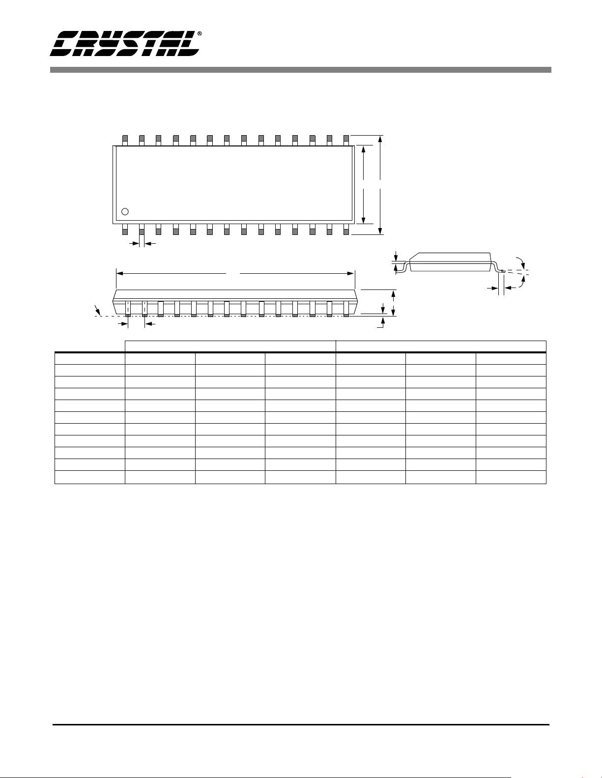
28L SOIC (300 MIL BODY) PACKAGE DRAWING
1
b
CS43122
HE
c
D
SEATING
PLANE
e
A
A1
INCHES MILLIMETERS
DIM MIN NOM MAX MIN NOM MAX
A 0.093 0.098 0.104 2.35 2.50 2.65
A1 0.004 0.008 0.012 0.10 0.20 0.30
b 0.013 0.017 0.020 0.33 0.42 0.51
C 0.009 0.011 0.013 0.23 0.28 0.32
D 0.697 0.705 0.713 17.70 17.90 18.10
E 0.291 0.295 0.299 7.40 7.50 7.60
e 0.040 0.050 0.060 1.02 1.27 1.52
H 0.394 0.407 0.419 10.00 10.34 10.65
L 0.016 0.026 0.050 0.40 0.65 1.27
∝
0° 4° 8° 0° 4° 8°
JEDEC #: MS-013
Controling Dimension is Millimeters
∝
L
26
Page 27

• Notes •
Page 28

 Loading...