

Page 1

`
Line Outputs
Pseudo Diff. Input
-
+
+VCP_FILT
-VCP_FILT
Digital Processing
Level Shifters
CS42L73
Decimator,
HPF,
Noise
Gate,
ALC,
Volume,
Mute,
Swap/Mono
Volume, Mute, Limiter
MCLK
Stereo
Multi-bit
DAC
MCLK
Stereo
Multi-bit
DAC
LDO
VD_FILT
Headphone Outputs
Pseudo Diff. Input
-
+
+VCP_FILT
-VCP_FILT
Ear Speaker Output
VA
-
+
B
Speakerphone Line
Output (Right)
-
+
VP
B
VP
Speakerphone Output
(Left)
-
+
VP
A
VA
VA
Digital MIC Interface
Digital MIC Interface
VL
MCLK
Stereo
Multi-bit
ADC
-6 to +12 dB,
0.5 dB steps
-
+
MIC 2
MIC 1
Pseudo Diff. Input
Pseudo Diff. Input
Line Input (Left)
Line Input (Right)
Pseudo Diff. Input
+10 or
+20 dB
-
+
+10 or
+20 dB
-
+
MIC 1 Bias
MIC 2 Bias
MIC Bias Short DetectMIC Bias
Audio Serial Port
Voice Serial Port
Auxiliary Serial Port
Audio
Serial Port
SDOUT
SDIN
ASRC
ASRC
Voice
Serial Port
SDOUT
ASRC
Auxiliary
Serial Port
SDIN
ASRC
SDOUT
ASRC
SDIN
ASRC
-VCP_FILT
Inverting
Step-Down
VCP +VCP_FILT
+VCP_FILT
-VCP_FILT
MCLK
MCLK1
MCLK2
Control Port
Control Port
VP
VD_FILT
Digital Mixer
Volume, Mute, Limiter
MIC2_SDET
+
Audio Serial Port
Voice Serial Port
Auxiliary Serial Port
MIC/Line Input Path
CS42L73
Ultralow Power Mobile Audio and Telephony CODEC
Product Overview
Stereo analog-to-digital converter (ADC)
Dual analog or digital mic support
Dual mic bias generators
Four digital-to-analog converters (DACs)
coupled to five outputs
– Ground-centered stereo headphone amp.
– Ground-centered stereo line output
– Mono ear speaker amplifier
– Mono 1-W speakerphone amplifier
– Mono speakerphone line output for stereo
speakerphone expansion
Three serial ports with asynchronous sample
rate converters
Digital audio mixing and routing
Ultralow Power Consumption
3.8-mW quiescent headphone playback
Applications
Smart phones, ultramobile PCs, and mobile
Internet devices
System Features
Native (no PLL required) support for 6/12/
24 MHz, 13/26 MHz, and 19.2/38.4 MHz
master clock rates and typical audio clock rates
Integrated high-efficiency power management
reduces power consumption
– Internal LDO regulator to reduce internal
digital operating voltage to VL/2 V
– Step-down charge pump provides low
headphone/line out supply voltage
– Inverting charge pump accommodates low
system voltage by providing negative rail for
HP and line amplifier
Flexible speakerphone amplifier powering
– 3.00–5.25 V range
– Independent cycling
Power-down management
– Individual controls for ADCs, digital mic
interface, mic bias generators, serial ports,
and output amplifiers and associated DACs
Programmable thermal overload notification
High-speed I²C™ control port (400 kHz)
(Features continued on page 2)
http://www.cirrus.com
Copyright Cirrus Logic, Inc. 2013
(All Rights Reserved)
JULY '13
DS882F1
Page 2

CS42L73
Stereo Analog-to-Digital Features
91-db dynamic range (A-weighted)
-85 dB THD+N
Independent ADC channel control
2:1 stereo analog input MUX
Stereo line input: Shared pseudodifferential
reference input
Dual analog mic inputs
– Pseudodifferential or single-ended
– Two, independent, programmable, low-noise
mic bias outputs
– Mic short detect to support headset button
Analog programmable gain amplifier (PGA)
(+12 to -6 dB in 0.5 dB steps)
+10 dB or +20 dB analog mic boost in addition
to PGA gain settings
Programmable automatic level control (ALC)
– Noise gate for noise suppression
– Programmable threshold and attack/release
rates
Dual Digital Microphone Interface
Programmable clock rate: Integer divide by 2 or
4 of internal MCLK
Stereo DAC to Headphone Amplifier
94-dB dynamic range (A-weighted)
-81 dB THD+N into 32
Integrated step-down/inverting charge pump
Class H amplifier, automatic supply adjustment
– High efficiency
–Low EMI
Pseudodifferential ground-centered outputs
High HP power output at -70/-81 dB THD+N
– 2 x 16/8.1 mW into 16/32 @ 1.8 V
Pop and click suppression
Analog volume control (+12 to -50 dB in 1 dB
steps; to -76 dB in 2 dB steps) with zero-cross
transitions
Digital volume control (+12 to -102 dB in 0.5 dB
steps) with soft-ramp transitions
Programmable peak-detect and limiter
Stereo DAC to Line Outputs
97 dB dynamic range (A-weighted)
-86 dB THD+N
Class-H amplifier
Pseudodifferential ground-centered outputs
1-V
Pop and click suppression
Analog volume control (+12 to -50 dB in 1 dB
line output @ 1.8 V
RMS
steps; to -76 dB in 2 dB steps) with zero-cross
transitions
Digital volume control (+12 to -102 dB in 0.5 dB
steps) with soft-ramp transitions
Programmable peak-detect and limiter
Mono DAC to Ear Speaker Amplifier
High-power output at -70 dB (0.032%) THD+N:
45 mW into 16 @ 1.8 V
Pop and click suppression
Digital volume control (+12 to -102 dB in 0.5 dB
steps) with soft-ramp transitions
Programmable peak-detect and limiter
Mono DAC to Speakerphone Amplifier
High output power at 1% THD+N: 1.06/0.76/
0.59 W into 8 @ 5.0/4.2/3.7 V
Direct battery-powered operation
Pop and click suppression
Digital volume control (+12 to -102 dB in 0.5 dB
steps) with soft-ramp transitions
Programmable peak-detect and limiter
Mono DAC-to-Speakerphone Line
Output
84 dB dynamic range (A-weighted)
-65 dB THD+N
High voltage (2 V
@ VA = 1.8 V, VP =
RMS
3.7 V) line output to ensure maximum output
from a wide variety of external amplifiers
Pop and click suppression
Digital volume control (+12 to -102 dB in 0.5 dB
steps) with soft-ramp transitions
Programmable peak-detect and limiter
Serial Ports
Three independent serial ports: auxiliary serial
port (XSP), audio serial port (ASP), and voice
serial port (VSP)
8.00, 11.025, 12.00, 16.00, 22.05, 24.00,
32.00, 44.10, and 48.00 kHz sample rates
All ports support master or slave operation with
I²S interface
XSP and VSP support slave operation with
PCM interface
XSP and ASP are stereo-input/stereo-output
to/from digital mixer
VSP is mono-input/stereo-output to/from digital
mixer
Integrated asynchronous sample rate
converters
2 DS882F1
Page 3

CS42L73
General Description
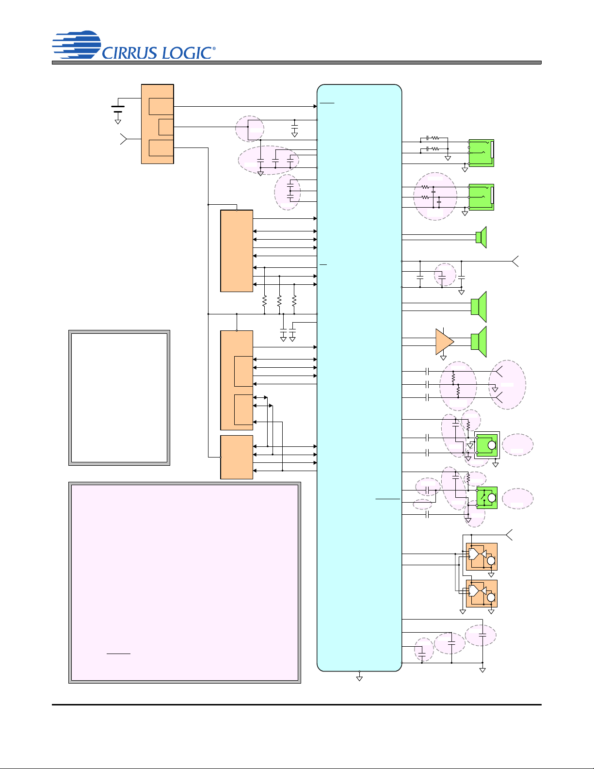
The CS42L73 is a highly integrated, low-power, audio and telephony CODEC for portable applications such as
smartphones and ultramobile personal computers.
The CS42L73 features a flexible clocking architecture, allowing the device to use reference clock frequencies of
6, 12, 24, 13, 26, 19.2, or 38.4 MHz, or any standard audio master clock. As many as two reference/master clock
sources may be connected; either one can be selected to drive the internal clocks and processing rate of the
CS42L73. Thus, multiple master clock sources within a system can be dynamically activated and deactivated to
minimize system-level power consumption.
Three asynchronous bidirectional serial ports (auxiliary, audio, and voice serial ports (XSP, ASP, and VSP,
respectively) support multiple clock domains of various digital audio sources or destinations. Three low-latency,
fast-locking, integrated high-performance asynchronous sample rate converters synchronize and convert the
audio samples to the internal processing rate of the CS42L73.
A stereo line input or two mono (one stereo) mic inputs are routed to a stereo ADC. The mic inputs may be
selectively preamplified by +10 or +20 dB. Two independent, low-noise mic bias voltage supplies are also provided.
A PGA is applied to the inputs before they reach the ADC.
The stereo input path that follows the stereo ADC begins with a multiplexer to selectively choose data from a
digital mic interface. Following the multiplexer, the data is decimated, selectively DC high-pass filtered,
channel-swapped or mono-to-stereo routed (fanned-out), and volume adjusted or muted. The volume levels can be
automatically adjusted via a programmable ALC and noise gate.
A digital mixer is used to mix and route the CS42L73’s inputs (analog inputs to ADC, digital mic, or serial ports) to
outputs (DAC-fed amplifiers or serial ports). There is independent attenuation on each mixer input for each output.
The processing along the output paths from the digital mixer to the two stereo DACs includes volume adjustment
and mute control. A peak-detector can be used to automatically adjust the volume levels via a programmable limiter.
The first stereo DAC feeds the stereo headphone and line output amplifiers, which are powered from a dedicated
positive supply. An integrated charge pump provides a negative supply. This allows a ground-centered analog
output with a wide signal swing, and eliminates external DC-blocking capacitors while reducing pops and clicks.
Tri-level Class H amplification is used to reduce power consumption under low-signal-level conditions. Analog
volume controls are provided on the stereo headphone and line outputs.
The second stereo DAC feeds several mono outputs. The left channel of the DAC sources a mono,
differential-drive, speakerphone amplifier for driving the handset speakerphone. The right channel sources a
mono, differential-drive, earphone amplifier for driving the handset earphone. The right channel is also routed to
a mono, differential-drive, speakerphone line output, which may be connected to an external amplifier to
implement a stereo speakerphone configuration when it is used in conjunction with the integrated speakerphone
amplifier.
The CS42L73 implements robust power management to achieve ultralow power consumption. High granularity in
power-down controls allows individual functional blocks to be powered down when unused. The internal low-dropout
regulator (LDO) saves power by running the internal digital circuits at half the logic interface supply voltage (VL/2).
A high-speed I
The CS42L73 is available in space-saving 64-ball WLCSP and 65-ball FBGA packages for the commercial (-40° to
+85° C) grade.
2
C control port interface capable of up to 400 kHz operation facilitates register programming.
DS882F1 3
Page 4

TABLE OF CONTENTS
1. PACKAGE PIN/BALL ASSIGNMENTS AND CONFIGURATIONS ..................................................... 12
1.1 64-Ball Wafer-Level Chip Scale Package (WLCSP) ...................................................................... 12
1.2 65-Ball Fine-Pitch Ball Grid Array (FBGA) Package ...................................................................... 13
1.3 Pin/Ball Descriptions ...................................................................................................................... 14
1.4 Digital Pin/Ball I/O Configurations .................................................................................................. 16
2. TYPICAL CONNECTION DIAGRAM ................................................................................................... 17
2.1 Low-Profile Charge-Pump Capacitors ........................................................................................... 18
2.2 Ceramic Capacitor Derating ........................................................................................................... 18
3. CHARACTERISTIC AND SPECIFICATIONS ...................................................................................... 19
4. APPLICATIONS ................................................................................................................................... 41
4.1 Overview ........................................................................................................................................ 41
4.1.1 Basic Architecture ................................................................................................................. 41
4.1.2 Line and Microphone Inputs .................................................................................................. 41
4.1.3 Line and Headphone Outputs (Class H, Ground-Centered Amplifiers) ................................. 41
4.1.4 Digital Mixer ........................................................................................................................... 41
4.1.5 Power Management .............................................................................................................. 41
4.2 Internal Master Clock Generation .................................................................................................. 42
4.3 Thermal Overload Notification ....................................................................................................... 42
4.4 Pseudodifferential Outputs ............................................................................................................. 43
4.5 Class H Amplifier .......................................................................................................................... 44
4.5.1 Power Control Options .......................................................................................................... 44
4.5.1.1 Standard Class AB Operation (Mode 001, 010, and 011) ......................................... 45
4.5.1.2 Adapt-to-Volume Settings (Mode 000) ...................................................................... 45
4.5.1.3 Adapt-to-Output Signal (Mode 111) ........................................................................... 46
4.5.2 Power Supply Transitions ...................................................................................................... 46
4.5.3 Efficiency ............................................................................................................................... 49
4.6 DAC Limiter .................................................................................................................................... 49
4.7 Analog Output Current Limiter ....................................................................................................... 51
4.8 Serial Ports .................................................................................................................................... 51
4.8.1 Power Management .............................................................................................................. 51
4.8.2 I/O .......................................................................................................................................... 51
4.8.3 High-impedance Mode .......................................................................................................... 52
4.8.4 Master and Slave Timing ....................................................................................................... 52
4.8.4.1 SCLK = MCLK Modes ............................................................................................... 53
4.8.5 Serial Port Sample Rates and Master Mode Settings ........................................................... 53
4.8.6 Formats ................................................................................................................................. 54
4.8.6.1 I²S Format .................................................................................................................. 55
4.8.6.2 PCM Format .............................................................................................................. 55
4.8.7 Mono/Stereo .......................................................................................................................... 57
4.8.8 Data Bit Depths ..................................................................................................................... 57
4.8.8.1 I²S Format Bit Depths ................................................................................................ 57
4.8.8.2 PCM Format Bit Depths ............................................................................................. 58
4.9 Asynchronous Sample Rate Converters (ASRCs) ......................................................................... 59
4.10 Input Paths ................................................................................................................................... 59
4.10.1 Input Path Source Selection and Powering ......................................................................... 59
4.10.2 Digital Microphone (DMIC) Interface ................................................................................... 60
4.10.2.1 DMIC Interface Description ...................................................................................... 60
4.10.2.2 DMIC Interface Signaling ......................................................................................... 60
4.10.2.3 DMIC Interface Powering ......................................................................................... 60
4.10.2.4 DMIC Interface Clock Generation ............................................................................ 61
4.11 Digital Mixer ................................................................................................................................. 61
4.11.1 Mono and Stereo Paths ....................................................................................................... 63
CS42L73
4 DS882F1
Page 5

CS42L73
4.11.2 Mixer Input Attenuation Adjustment .................................................................................... 63
4.11.3 Powered-Down Mixer Inputs ...............................................................................................64
4.11.4 Avoiding Mixer Clipping ....................................................................................................... 64
4.11.5 Mixer Attenuation Values .................................................................................................... 65
4.12 Recommended Operating Procedures ........................................................................................ 65
4.12.1 Initial Power-Up Sequence .................................................................................................. 65
4.12.2 Power-Up Sequence (xSP to HP/LO) ................................................................................. 66
4.12.3 Power-Down Sequence (xSP to HP/LO) ............................................................................. 67
4.12.4 Recommended Sequence for Modification of the MCLK Signal ......................................... 67
4.12.5 Microphone Enabling/Switching Sequence ......................................................................... 68
4.12.6 Final Power-Down Sequence .............................................................................................. 68
4.13 Using MIC2_SDET as Headphone Plug Detect ........................................................................... 69
4.14 Headphone Plug Detect and Mic Short Detect ............................................................................ 70
4.15 Interrupts ...................................................................................................................................... 70
4.16 Control Port Operation ................................................................................................................. 71
4.16.1 I²C Control ........................................................................................................................... 71
4.17 Fast Start Mode ........................................................................................................................... 73
4.18 Headphone High-Impedance Mode .............................................................................................75
5. REGISTER QUICK REFERENCE ........................................................................................................ 76
6. REGISTER DESCRIPTION .................................................................................................................. 81
6.1 Fast Mode Enable (Address 00h) .................................................................................................. 81
6.1.1 Test Bits ................................................................................................................................ 81
6.2 Device ID A and B (Address 01h), C and D (Address 02h), and E (Address 03h) (Read Only) . 81
6.2.1 Device I.D. (Read Only) ........................................................................................................ 81
6.3 Revision ID (Address 05h) (Read Only) ......................................................................................... 81
6.3.1 Alpha Revision (Read Only) .................................................................................................. 81
6.3.2 Metal Revision (Read Only) .................................................................................................. 81
6.4 Power Control 1 (Address 06h) ...................................................................................................... 82
6.4.1 Power Down ADC x ............................................................................................................... 82
6.4.2 Power Down Digital Mic x ...................................................................................................... 82
6.4.3 Discharge Filt+ Capacitor ...................................................................................................... 82
6.4.4 Power Down Device .............................................................................................................. 82
6.5 Power Control 2 (Address 07h) ...................................................................................................... 83
6.5.1 Power Down MICx Bias ......................................................................................................... 83
6.5.2 Power Down VSP .................................................................................................................. 83
6.5.3 Power Down ASP SDOUT Path ............................................................................................ 83
6.5.4 Power Down ASP SDIN Path ................................................................................................ 83
6.5.5 Power Down XSP SDOUT Path ............................................................................................ 83
6.5.6 Power Down XSP SDIN Path ................................................................................................
6.6 Power Control 3 and Thermal Overload Threshold Control (Address 08h) ................................... 84
6.6.1 Thermal Overload Threshold Settings ................................................................................... 84
6.6.2 Power Down Thermal Sense .................................................................................................84
6.6.3 Power Down Speakerphone Line Output .............................................................................. 84
6.6.4 Power Down Ear Speaker ..................................................................................................... 84
6.6.5 Power Down Speakerphone ..................................................................................................84
6.6.6 Power Down Line Output ...................................................................................................... 85
6.6.7 Power Down Headphone ...................................................................................................... 85
6.7 Charge Pump Frequency and Class H Configuration (Address 09h) ............................................ 85
6.7.1 Charge Pump Frequency ...................................................................................................... 85
6.7.2 Adaptive Power Adjustment .................................................................................................. 85
6.8 Output Load, Mic Bias, and MIC2 Short Detect Configuration (Address 0Ah) ............................... 86
6.8.1 VP Supply Minimum Voltage Setting ..................................................................................... 86
6.8.2 Speakerphone Light Load Mode Enable ............................................................................... 86
6.8.3 Mic Bias Output Control ........................................................................................................ 86
83
DS882F1 5
Page 6

CS42L73
6.8.4 Short Detect Automatic Mute Control .................................................................................... 86
6.9 Digital Mic and Master Clock Control (Address 0Bh) ..................................................................... 87
6.9.1 Digital Mic Shift Clock Divide Ratio ....................................................................................... 87
6.9.2 Master Clock Source Selection ............................................................................................. 87
6.9.3 Master Clock Divide Ratio ..................................................................................................... 87
6.9.4 Master Clock Disable ............................................................................................................ 87
6.10 XSP Control (Address 0Ch) ......................................................................................................... 88
6.10.1 Tristate XSP Interface ......................................................................................................... 88
6.10.2 XSP Digital Interface Format ............................................................................................... 88
6.10.3 XSP PCM Interface Mode ................................................................................................... 88
6.10.4 XSP PCM Format Bit Order ................................................................................................88
6.10.5 XSP SCLK Source Equals MCLK ....................................................................................... 88
6.11 XSP Master Mode Clocking Control (Address 0Dh) .................................................................... 89
6.11.1 XSP Master/Slave Mode ..................................................................................................... 89
6.11.2 XSP Master Mode Clock Control Dividers ........................................................................... 89
6.12 ASP Control (Address 0Eh) ......................................................................................................... 89
6.12.1 Tristate ASP Interface ......................................................................................................... 89
6.12.2 ASP Sample Rate ............................................................................................................... 90
6.12.3 ASP SCLK Source Equals MCLK ....................................................................................... 90
6.13 ASP Master Mode Clocking Control (Address 0Fh) ..................................................................... 90
6.13.1 ASP Master/Slave Mode ..................................................................................................... 90
6.13.2 ASP Master Mode Clock Control Dividers ........................................................................... 90
6.14 VSP Control (Address 10h) .......................................................................................................... 91
6.14.1 Tristate VSP Interface .................................................................................................
6.14.2 VSP Digital Interface Format ............................................................................................... 91
6.14.3 VSP PCM Interface Mode ................................................................................................... 91
6.14.4 VSP PCM Format Bit Order ................................................................................................91
6.14.5 VSP SDIN Location ............................................................................................................. 92
6.14.6 VSP SCLK Source Equals MCLK ....................................................................................... 92
6.15 VSP Master Mode Clocking Control (Address 11h) ..................................................................... 92
6.15.1 VSP Master/Slave Mode ..................................................................................................... 92
6.15.2 VSP Master Mode Clock Control Dividers ........................................................................... 92
6.16 VSP and XSP Sample Rate (Address 12h) ................................................................................. 93
6.16.1 VSP Sample Rate ............................................................................................................... 93
6.16.2 XSP Sample Rate ............................................................................................................... 93
6.17 Miscellaneous Input and Output Path Control (Address 13h) ...................................................... 94
6.17.1 Digital Swap/Mono .............................................................................................................. 94
6.17.2 Input Path Channel B=A ...................................................................................................... 94
6.17.3 PREAMP and PGA Channel B=A ....................................................................................... 94
6.17.4 PGA Soft-Ramp ................................................................................................................... 95
6.17.5 Analog Zero Cross .............................................................................................................. 95
6.17.6 Digital Soft-Ramp ................................................................................................................ 96
6.17.7 Analog Output Soft Ramp ................................................................................................... 96
6.18 ADC/Input Path Control (Address 14h) ........................................................................................ 97
6.18.1 PGA x Input Select .............................................................................................................. 97
6.18.2 Boost x ................................................................................................................................ 97
6.18.3 Invert ADCx Signal Polarity ................................................................................................. 97
6.18.4 Input Path x Digital Mute ..................................................................................................... 97
6.19 Mic PreAmp and PGA Volume Control: Channel A (Mic 1, Address 15h) and Channel B
(Mic 2, Address 16h) .......................................................................................................................... 98
6.19.1 Mic PREAMP x Volume ....................................................................................................... 98
6.19.2 PGAx Volume ...................................................................................................................... 98
6.20 Input Path x Digital Volume Control: Channel A (Address 17h) and B (Address 18h) ................. 99
6.20.1 Input Path x Digital Volume Control .................................................................................... 99
........ 91
6 DS882F1
Page 7

CS42L73
6.21 Playback Digital Control (Address 19h) ..................................................................................... 100
6.21.1 Speakerphone [A], Ear Speaker/Speakerphone Line Output [B] (SES) Playback
Channels B=A ............................................................................................................................ 100
6.21.2 Headphone/Line Output (HL) Playback Channels B=A .................................................... 100
6.21.3 Limiter Soft-Ramp Disable ................................................................................................ 100
6.21.4 Ear Speaker/Speakerphone Line Output Digital Mute ...................................................... 100
6.21.5 Speakerphone Digital Mute ...............................................................................................101
6.21.6 Headphone/Line Output (HL) x Digital Mute ..................................................................... 101
6.22 Headphone/Line Output (HL) x Digital Volume Control: Channel A (Address 1Ah) and B
(Address 1Bh) .................................................................................................................................. 101
6.22.1 Headphone/Line Output (HL) x Digital Volume Control ..................................................... 101
6.23 Speakerphone Out [A] Digital Volume Control (Address 1Ch) .................................................. 102
6.23.1 Speakerphone Out [A] Digital Volume Control .................................................................. 102
6.24 Ear Speaker/Speakerphone Line Output (ESL) [B] Digital Volume Control (Address 1Dh) ...... 102
6.24.1 Ear Speaker/Speakerphone Line Output (ESL) [B] Digital Volume Control ...................... 102
6.25 Headphone Analog Volume Control: Channel A (Address 1Eh) and B (Address 1Fh) ............. 103
6.25.1 Headphone x Analog Mute ................................................................................................ 103
6.25.2 Headphone x Analog Volume Control ............................................................................... 103
6.26 Line Output Analog Volume Control: Channel A (Address 20h) and B (Address 21h) .............. 104
6.26.1 Line Output x Analog Mute ................................................................................................ 104
6.26.2 Line Output x Analog Volume Control ............................................................................... 104
6.27 Stereo Input Path Advisory Volume (Address 22h) ................................................................... 105
6.27.1 Stereo Input Path Advisory Volume .................................................................................. 105
6.28 XSP Input Advisory Volume (Address 23h) ............................................................................... 105
6.28.1 XSP Input Advisory Volume .............................................................................................. 105
6.29 ASP Input Advisory Volume (Address 24h) ............................................................................... 106
6.29.1 ASP Input Advisory Volume .............................................................................................. 106
6.30 VSP Input Advisory Volume (Address 25h) ............................................................................... 106
6.30.1 VSP Input Advisory Volume .............................................................................................. 106
6.31 Limiter Attack Rate Headphone/Line Output (HL) (Address 26h) .............................................. 107
6.31.1 Limiter Attack Rate HL ...................................................................................................... 107
6.32 Limiter Control, Release Rate Headphone/Line Output (HL) (Address 27h) ............................. 107
6.32.1 Peak Detect and Limiter HL ..............................................................................................107
6.32.2 Peak Signal Limit All Channels HL .................................................................................... 107
6.32.3 Limiter Release Rate HL ................................................................................................... 107
6.33 Limiter Min/Max Thresholds Headphone/Line Output (HL) (Address 28h) ................................ 108
6.33.1 Limiter Maximum Threshold HL ........................................................................................ 108
6.33.2 Limiter Cushion Threshold HL ........................................................................................... 108
6.34 Limiter Attack Rate Speakerphone [A] (Address 29h) ............................................................... 108
6.34.1 Limiter Attack Rate Speakerphone [A] .............................................................................. 108
6.35 Limiter Control, Release Rate Speakerphone [A] (Address 2Ah) .............................................. 109
6.35.1 Peak Detect and Limiter Speakerphone [A] ...................................................................... 109
6.35.2 Peak Signal Limit All Channels Speakerphone ................................................................. 109
6.35.3 Limiter Release Rate Speakerphone [A] ........................................................................... 109
6.36 Limiter Min/Max Thresholds Speakerphone [A] (Address 2Bh) ................................................. 110
6.36.1 Limiter Maximum Threshold Speakerphone [A] ................................................................ 110
6.36.2 Limiter Cushion Threshold Speakerphone [A] ................................................................... 110
6.37 Limiter Attack Rate Ear Speaker/Speakerphone Line Output (ESL) [B] .................................... 111
6.37.1 Limiter Attack Rate ESL [B] ............................................................................................... 111
6.38 Limiter Control, Release Rate Ear Speaker/Speakerphone Line Output (ESL) [B]
(Address 2Dh) .................................................................................................................................. 111
6.38.1 Peak Detect and Limiter ESL [B] ....................................................................................... 111
6.38.2 Limiter Release Rate ESL [B] ............................................................................................111
6.39 Limiter Min/Max Thresholds Ear Speaker/Speakerphone Line Output (ESL) [B] ...................... 112
DS882F1 7
Page 8

CS42L73
6.39.1 Limiter Maximum Threshold ESL [B] ................................................................................. 112
6.39.2 Limiter Cushion Threshold ESL [B] ................................................................................... 112
6.40 ALC Enable and Attack Rate AB (Address 2Fh) ........................................................................ 113
6.40.1 ALC for Channels A and B (ALCx) .................................................................................... 113
6.40.2 ALC Attack Rate for Channels A and B ............................................................................. 113
6.41 ALC Release Rate AB (Address 30h) ........................................................................................ 113
6.41.1 ALC Release Rate for Channels A and B ......................................................................... 113
6.42 ALC Threshold AB (Address 31h) .............................................................................................. 114
6.42.1 ALC Maximum Threshold for Channels A and B ............................................................... 114
6.42.2 ALC Minimum Threshold for Channels A and B ................................................................ 114
6.43 Noise Gate Control AB (Address 32h) .......................................................................................115
6.43.1 Noise Gate Enable for Channels A and B (NGx) .............................................................. 115
6.43.2 Noise gate Threshold and Boost for Channels A and B .................................................... 115
6.43.3 Noise Gate Delay Timing for Channels A and B ............................................................... 115
6.44 ALC and Noise Gate Misc Control (Address 33h) ..................................................................... 116
6.44.1 ALC Ganging of Channels A and B ................................................................................... 116
6.44.2 Noise Gate Ganging of Channels A and B ........................................................................ 116
6.44.3 ALCx Soft-Ramp Disable ..................................................................................................116
6.44.4 ALCx Zero Cross Disable .................................................................................................. 116
6.45 Mixer Control (Address 34h) ..................................................................................................... 117
6.45.1 VSP Mixer Output Stereo .................................................................................................. 117
6.45.2 XSP Mixer Output Stereo .................................................................................................. 117
6.45.3 Mixer Soft-Ramp Enable ................................................................................................... 117
6.45.4 Mixer Soft-Ramp Step Size/Period .................................................................................... 117
6.46 Stereo Mixer Input Attenuation (Addresses 35h through 54h) ................................................... 118
6.46.1 Stereo Mixer Input Attenuation ..........................................................................................119
6.47 Mono Mixer Controls (Address 55h) .......................................................................................... 120
6.47.1 Speakerphone (SPK) Mixer, ASP Select .......................................................................... 120
6.47.2 Speakerphone (SPK) Mixer, XSP Select .......................................................................... 120
6.47.3 Ear Speaker/Speakerphone Line Output (ESL) Mixer, ASP Select .................................. 120
6.47.4 ESL Mixer, Auxiliary Serial Port (XSP) Select ................................................................... 120
6.48 Mono Mixer Input Attenuation (Addresses 56h through 5Dh) .................................................... 121
6.48.1 Mono Mixer Input Attenuation ........................................................................................... 121
6.49 Interrupt Mask Register 1 (Address 5Eh) ...................................................................................122
6.50 Interrupt Mask Register 2 (Address 5Fh) ...................................................................................122
6.51 Interrupt Status Register 1 (Address 60h) .................................................................................122
6.51.1 MIC2 Short Detect ............................................................................................................. 122
6.51.2 Thermal Overload Detect .................................................................................................. 122
6.51.3 Digital Mixer Overflow ....................................................................................................... 123
6.51.4 Input Path x Overflow ........................................................................................................ 123
6.52 Interrupt Status Register 2 (Address 61h) .................................................................................123
6.52.1 Voice ASRC Data Out Lock .............................................................................................. 123
6.52.2 Voice ASRC Data In Lock .................................................................................................123
6.52.3 Audio ASRC Data Out Lock .............................................................................................. 124
6.52.4 Audio ASRC Data In Lock .................................................................................................124
6.52.5 Auxiliary ASRC Data Out Lock .......................................................................................... 124
6.52.6 Auxiliary ASRC Data In Lock .............................................................................................124
6.53 Fast Mode 1 (Address 7Eh) ....................................................................................................... 125
6.53.1 Fast Mode Bits 15:8 .......................................................................................................... 125
6.54 Fast Mode 2 (Address 7Fh) ....................................................................................................... 125
6.54.1 Fast Mode Bits 7:0 ............................................................................................................ 125
7. PCB LAYOUT CONSIDERATIONS ...................................................................................................125
7.1 Power Supply ............................................................................................................................... 125
7.2 Grounding .................................................................................................................................... 125
8 DS882F1
Page 9

CS42L73
7.3 Layout With Fine-Pitch, Ball-Grid Packages ................................................................................ 125
8. PERFORMANCE DATA ..................................................................................................................... 126
8.1 Analog Input Path Attributes ........................................................................................................ 126
8.1.1 PGA Analog Volume Nonlinearity (DNL and INL) ............................................................... 126
8.2 Analog Mic/Line ADC and Digital Mic Input Path Attributes ......................................................... 127
8.2.1 Input Path Digital LPF Response ........................................................................................ 127
8.2.2 Input Path Digital HPF Response ........................................................................................ 128
8.3 Core Circuitry Attributes ............................................................................................................... 129
8.3.1 ASRC Attributes .................................................................................................................. 129
8.3.1.1 Response ................................................................................................................. 129
8.3.1.2 Group Delay ............................................................................................................. 130
8.3.1.3 Lock Time ................................................................................................................ 130
8.4 Analog Output Paths Attributes .................................................................................................... 131
8.4.1 DAC Digital LPF Response .................................................................................................131
8.4.2 DAC HPF Response ........................................................................................................... 132
8.4.3 Output Analog Volume Nonlinearity (DNL and INL) ............................................................ 132
8.4.4 Startup Times ...................................................................................................................... 133
9. PARAMETER DEFINITIONS .............................................................................................................. 134
10. PACKAGE DIMENSIONS ................................................................................................................ 135
10.1 WLCSP Package ....................................................................................................................... 135
10.2 FBGA Package .......................................................................................................................... 136
11. THERMAL CHARACTERISTICS ..................................................................................................... 137
12. ORDERING INFORMATION ............................................................................................................ 137
13. REFERENCES .................................................................................................................................. 137
14. REVISION HISTORY ........................................................................................................................ 138
LIST OF FIGURES
Figure 1.Typical Connection Diagram ....................................................................................................... 17
Figure 2.MICx Dynamic Range Test Configuration ................................................................................... 24
Figure 3.Analog Input CMRR Test Setup .................................................................................................. 24
Figure 4.LINEIN_REF/MICx_REF Input Voltage Test Setup .................................................................... 24
Figure 5.Headphone Output Test Configuration ....................................................................................... 28
Figure 6.Line Output Test Configuration ................................................................................................... 29
Figure 7.Ear Speaker Output Test Configuration ...................................................................................... 30
Figure 8.Speakerphone and Speakerphone Line Output Test Configuration ........................................... 32
Figure 9.Power Consumption Test Configuration ..................................................................................... 34
Figure 10.Power and Reset Sequencing .................................................................................................. 36
Figure 11.Digital Mic Interface Timing ....................................................................................................... 37
Figure 12.Serial Port Interface Timing—I²S Format .................................................................................. 39
Figure 13.Serial Port Interface Timing—PCM Format ..............................................................................39
Figure 14.I²C Control Port Timing ............................................................................................................. 40
Figure 15.Single-Ended Output Configuration .......................................................................................... 43
Figure 16.Pseudodifferential Output Configuration ................................................................................... 43
Figure 17.Class H Operation ..................................................................................................................... 44
Figure 18.Class H Control - Adapt-to-Volume Mode ................................................................................. 45
Figure 19.VCP_FILT Transitions ............................................................................................................... 47
Figure 20.VCP_FILT Hysteresis ............................................................................................................... 48
Figure 21.Input Power vs. Output Power .................................................................................................. 49
Figure 22.Peak Detect & Limiter ............................................................................................................... 50
Figure 23.HP Short Circuit Setup .............................................................................................................. 51
Figure 24.Line Short Circuit Setup ............................................................................................................ 51
Figure 25.Serial Port Busing when Mastering Timing ............................................................................... 52
Figure 26.Serial Port Busing When Slave Timed ...................................................................................... 52
DS882F1 9
Page 10

CS42L73
Figure 27.I²S Format ................................................................................................................................. 55
Figure 28.PCM Format—Mode 0 .............................................................................................................. 56
Figure 29.PCM Format—Mode 1 .............................................................................................................. 56
Figure 30.PCM Format—Mode 2 .............................................................................................................. 57
Figure 31.Digital Mic Interface Signaling ................................................................................................... 60
Figure 32.Digital Mixer Diagram ................................................................................................................ 62
Figure 33.Connection Diagram for Using MIC2_SDET as Headphone Detect ......................................... 69
Figure 34.Flow Diagram Showing the INT
Figure 35.Connection Diagram for Headphone Detect with Additional Short Detect ................................ 70
Figure 36.Example of Rising-Edge Sensitive, Sticky, Interrupt Status Bit Behavior ................................. 71
Figure 37.Control Port Timing, I²C Writes with Autoincrement ................................................................. 72
Figure 38.Control Port Timing, I²C Reads with Autoincrement ................................................................. 72
Figure 39.Control Port Timing, I²C Reads with Preamble and Autoincrement .......................................... 73
Figure 40.Fast Start Pop ........................................................................................................................... 74
Figure 41.Start Up Transition Diagram ..................................................................................................... 75
Figure 42.PGA DNL ................................................................................................................................ 126
Figure 43.PGA INL .................................................................................................................................. 126
Figure 44.PGA + Preamp (+10 dB) DNL ................................................................................................. 126
Figure 45.PGA + Preamp (+10 dB) INL .................................................................................................. 126
Figure 46.PGA + Preamp (+20 dB) DNL ................................................................................................. 127
Figure 47.PGA + Preamp (+20 dB) INL .................................................................................................. 127
Figure 48.Input Path LPF Frequency Response ..................................................................................... 127
Figure 49.Input Path LPF Stopband Rejection ........................................................................................ 127
Figure 50.Input Path LPF Transition Band .............................................................................................. 128
Figure 51.Input Path LPF Transition Band Detail .................................................................................... 128
Figure 52.Input Path HPF Frequency Response ....................................................................................128
Figure 53.ASRC Frequency Response ................................................................................................... 129
Figure 54.ASRC Passband Frequency Response .................................................................................. 129
Figure 55.ASRC Group Delay vs. Serial Port and Internal Sample Rates .............................................. 130
Figure 56.DAC LPF Frequency Response .............................................................................................. 131
Figure 57.DAC LPF Stopband Rejection to 1x Fs ................................................................................... 131
Figure 58.DAC LPF Stopband Rejection to 3x Fs ................................................................................... 131
Figure 59.DAC HPF Frequency Response ............................................................................................. 132
Figure 60.HPOUTx DNL (-50 to +12 dB) ................................................................................................ 132
Figure 61.HPOUTx DNL (-76 to -52 dB) ................................................................................................. 132
Figure 62.HPOUTx INL (-50 to +12 dB) .................................................................................................. 132
Figure 63.HPOUTx INL (-76 to -52 dB) ................................................................................................... 132
Figure 64.LINEOUTx DNL (-50 to +12 dB) ............................................................................................. 133
Figure 65.LINEOUTx DNL (-76 to -52 dB) .............................................................................................. 133
Figure 66.LINEOUTx INL (-50 to +12 dB) ............................................................................................... 133
Figure 67.LINEOUTx INL (-76 to -52 dB) ................................................................................................ 133
Pin State in Response to MIC2_SDET State Changes .......... 69
LIST OF TABLES
Table 1. Internal Master Clock Generation ............................................................................................... 42
Table 2. Example of Impedance in Reference Path .................................................................................. 44
Table 3. Current through VCP with Varying Short Circuits .......................................................................51
Table 4. Supported MCLK1/MCLK2 Rates for Pre-MCLK Mode .............................................................. 53
Table 5. Serial Port Rates and Master Mode Settings .............................................................................. 53
Table 6. Actual xSP_LRCK Rate/Deviation Selector for Note 3 ............................................................... 54
Table 7. Supported Serial Port Formats .................................................................................................... 54
Table 8. Input Path Source Select and Digital Power States .................................................................... 59
Table 9. Digital Mic Interface Power States .............................................................................................. 60
Table 10. Digital Microphone Interface Clock Generation ......................................................................... 61
10 DS882F1
Page 11

CS42L73
Table 11. Digital Mixer Soft Ramp Rates .................................................................................................. 63
Table 12. Digital Mixer Nonclipping Attenuation Settings ......................................................................... 64
Table 13. Start Up Times .......................................................................................................................... 73
Table 14. Start Up Transition Values ........................................................................................................ 75
Table 15. ASRC Lock Times ................................................................................................................... 130
Table 16. Analog Output Startup Times .................................................................................................. 133
Table 17. WLCSP Package Dimensions ................................................................................................. 135
Table 18. FBGA Package Dimensions .................................................................................................... 136
DS882F1 11
Page 12
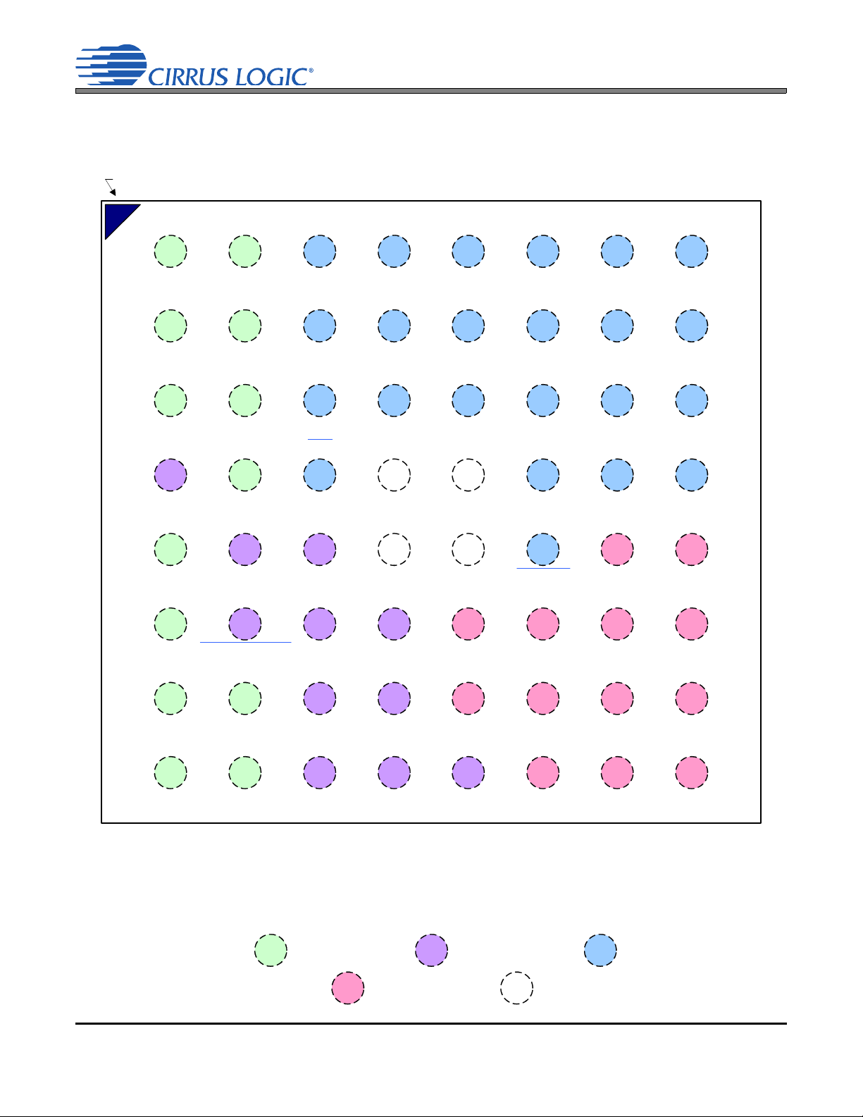
1. PACKAGE PIN/BALL ASSIGNMENTS AND CONFIGURATIONS
Top-Down
(Though Package)
View
H5
SPK_VQ
XSP_SDIN
DGND
B5
LINEINA
A5
MIC1
H6
HPOUTA
-VCP_FILT
XSP_SCLK
B6
ASP_LRCK
A6
XSP_SDOUT
H1 H2
B1 B2
A1 A2
H3 H4
VA
EAROUT-
B3 B4
LINEIN_REF
A3
LINEINB
A4
H7 H8
VL
B7
ASP_SDOUT
B8
A7
MCLK1
A8
ASP_SDIN
VD_FILT
Ball A1 Location Indicator
VP HPOUTB
DMIC_SCLK
PGND
C5
MIC2
C6
XSP_LRCK
DMIC_SD
C1 C2 C3 C4
MIC1_REF
VSP_SDOUT
C7
ASP_SCLK
C8
VSP_SDIN
SCL
D5
MICB_FILT
D6
THERM
D1 D2 D3 D4
MIC2_REF
VSP_SCLK
D7
MCLK2
D8
VSP_LRCK
E5
ANA_VQ
E6
THERM
THERM
E1 E2 E3 E4
MIC2_BIAS
VCP
E7 E8
FLYP
F5
FILT+
F6
LINEOUTB
SPKLINEO+
F1 F2 F3 F4
+VCP_FILT
F7
LINEOUTA
F8
FLYC
SPKLINEO-
G5
AGND
G6
LINEO_REF
SPKOUT+
G1 G2 G3 G4
EAROUT+
CPGND
G7
HPOUT_REF
G8
FLYN
SPKOUT-
SDA
INT
THERM
RESET
MIC2_SDET
MIC1_BIAS
VA I/O VL I/OVP I/O
VCP I/O Ground
1.1 64-Ball Wafer-Level Chip Scale Package (WLCSP)
CS42L73
12 DS882F1
Page 13
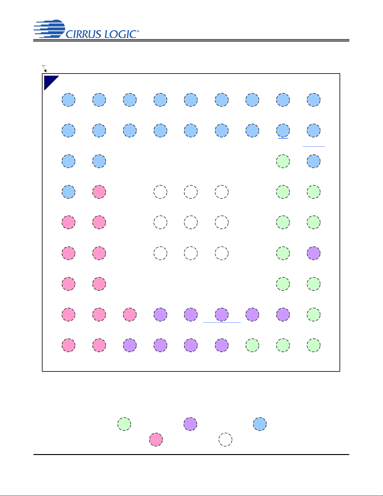
1.2 65-Ball Fine-Pitch Ball Grid Array (FBGA) Package
Top-Down
(Though Package)
View
H5
SPKLINEO-
ASP_LRCK
DMIC_SD
B5
VL
A5
VSP_SDIN
H6
MIC1_BIAS
MIC2_BIAS
ASP_SDOUT
B6
XSP_SDIN
A6
ASP_SCLK
H1 H2
B1 B2
A1 A2
H3 H4
-VCP_FILT
HPOUT_REF
B3 B4
VD_FILT
A3
MCLK2
A4
H7 H8
DMIC_SCLK
B7
XSP_SDOUT
B8
A7
XSP_SCLK
A8
XSP_LRCK
Ball A1 Location Indicator
SPKLINEO+
MCLK1
LINEO_REF
VSP_SDOUT
C1 C2
VSP_SCLK
C8
LINEIN_REF
D5
VSP_LRCK
D6
GND
D1 D2 D4
VCP GND
D8
LINEINA
E5
FLYP
E6
GND
GND
E1 E2 E4
+VCP_FILT
E8
MIC2_REF
F5
FLYC
F6
GND
GND
F1 F2 F4
GND
F8
MIC1_REF
FLYN
G1 G2
LINEOUTA
G8
MIC1
VA I/O VL I/OVP I/O
ASP_SDIN
GND
GND
LINEOUTB
SCL
FILT+
H9
B9
A9
SDA
C9
D9
LINEINB
E9
MIC2
F9
MICB_FILT
G9
ANA_VQ
J5
VP
J6
EAROUT-
EAROUT+
J1 J2 J3 J4
HPOUTA
HPOUTB
J7 J8
SPKOUT+ SPKOUT-
SPK_VQ VA
J9
INT
RESET
MIC2_SDET
VCP I/O Ground
CS42L73
DS882F1 13
Page 14
1.3 Pin/Ball Descriptions
Name Location Description
WLCSP FBGA
MCLK1
MCLK2
RESET
SCL C3 A9 Serial Control Port Clock (Input)
A6
D6
B3B2High Speed Clock (Input). Potential clock sources for the converters and the device core. Clock
source for optional serial port mastering.
E6 C9 Reset (Input). The device enters a low-power mode when this pin is driven low.
. Serial clock for the I²C control interfaces.
CS42L73
SDA A3 B9 Serial Control Data (Input/Output)
INT
LINEINA
LINEINB
LINEIN_REF A2 C8
MIC1
MIC2
MIC1_REF
MIC2_REF
MIC1_BIAS
MIC2_BIAS
D3 B8 Interrupt Request (Output). Open-drain active low interrupt request output.
A1
B2
D8D9Analog Line Inputs, A and B (LEFT and RIGHT) (Input)
Analog Input Characteristics specification table.
Analog Line Input Pseudodifferential Reference (Input)
input buffers LINEINA and LINEINB.
B1
C1
C2
D2
E3
E2
G8E9Microphone Inputs 1 and 2 (Input)
inputs. The full-scale level is specified in the Analog Input Characteristics specification table.
F8E8Microphone Inputs 1 and 2 Pseudodifferential References (Input)
microphone inputs MIC1 and MIC2.
H7
Microphone Bias Voltages 1 and 2 (Output)
H8
Microphone 2 Short Detect (Input)
MIC2_SDET
F2 H6
interrupts that represent the pressing and releasing of a button that shorts the headset
. SDA is the bidirectional data pin for the I²C control interface.
. The full-scale level is specified in the
. Ground reference for the analog line
. The handset (MIC1) and headset (MIC2) microphone signal
. Ground references for the
. Bias voltage for the microphones MIC1 and MIC2.
. Transitions on this input can be configured to cause
microphone to ground.
DMIC_SCLK B3 B7 Digital Mic Serial Clock (Output). The high-speed clock output to the digital microphone(s).
DMIC_SD
XSP_SCLK
XSP_LRCK C5 A7
C4 A8
A4 A6
Digital Mic Serial Data (Input)
Auxiliary Serial Port (XSP), Serial Clock (Input/Output)
XSP, Left/Right Clock (Input/Output)
. The serialized data input from the digital microphone(s).
. Serial shift clock for the interface.
. Identifies the start of each serialized PCM data word. When
the I²S interface format is selected, this signal also indicates which channel, Left or Right, is
currently active on the serial PCM audio data lines.
XSP_SDIN A5 B5 XSP, Data Input (Input)
XSP_SDOUT B4 B6 XSP, Data Output (Output)
. Input for two’s complement serial PCM audio data.
. Output for two’s complement serial PCM audio data.
ASP_SCLK C6 B4 Audio Serial Port (ASP), Serial Clock (Input/Output)
ASP_LRCK B5 A5
ASP_SDIN A7 A3 ASP, Data Input (Input)
ASP, Left/Right Clock (Input/Output)
indicates which channel, Left or Right, is currently active on the serial PCM audio data lines.
. Input for two’s complement serial PCM audio data.
ASP_SDOUT B6 A4 ASP, Data Output (Output)
. Output for two’s complement serial PCM audio data.
. Identifies the start of each serialized PCM data word and
VSP_SCLK D7 C2 Voice Serial Port (VSP), Serial Clock (Input/Output)
Voice Serial Port, Left/Right Clock (Input/Output)
VSP_LRCK D8 D1
data word. When the I²S interface format is selected, this signal also indicates which channel, Left
. Serial shift clock for the interface.
. Serial shift clock for the interface.
. Identifies the start of each serialized PCM
or Right, is currently active on the serial PCM audio data lines.
VSP_SDIN C8 B1 VSP, Data Input (Input)
VSP_SDOUT C7 C1 VSP, Data Output (Output)
HPOUTA
HPOUTB
HPOUT_REF G6 H2
H7
H6
J1J2Headphone Audio Output (Output)
Characteristics specification table.
Pseudodifferential Headphone Output Reference (Input)
amplifiers.
. Input for two’s complement serial PCM audio data.
. Output for two’s complement serial PCM audio data.
. The full-scale output level is specified in the HP Output
. Ground reference for the headphone
14 DS882F1
Page 15
Name Location Description
WLCSP FBGA
LINEOUTA
LINEOUTB
F6
F5
G2F2Line Audio Output (Output). The full-scale output level is specified in the Line Output
Characteristics specification table.
LINEO_REF G5 H3 Pseudodifferential Line Output Reference (Input)
EAROUT+
EAROUT-
SPKOUT+
SPKOUT-
SPKLINEO+
SPKLINEO-
VA H1 J9 Analog Power (Input)
VP
G2
J8J7Ear Speaker Audio Output (Output)
H2
G4
J4J6Speakerphone Audio Output (Output)
G3
F4
H4H5Speakerphone Audio Line Output (Output)
F3
H4 J5
Output Characteristics specification table.
Speakerphone Output Characteristics specification table.
Speakerphone Line Output Characteristics specification table.
. Power supply for the internal analog section.
Speakerphone Power (Input)
generators.
VCP E7 D2 Step-down Charge Pump Power (Input)
VL B7 A1
+VCP_FILT F7 E2
-VCP_FILT
FLYP
H8 H1
E8 E1
FLYC F8 F1
FLYN G8 G1
VD_FILT B8 A2
Digital Interface/Core Power (Input)
port, and digital mic interface. Power supply for the digital core logic step-down regulator.
Step-down Charge Pump Filter Connection (Output)
pump that provides the positive rail for the headphone and line amplifiers.
Inverting Charge Pump Filter Connection (Output)
pump that provides the negative rail for the headphone and line amplifiers.
Charge Pump Cap Positive Node (Output)
step-down charge pump’s flying capacitor.
Charge Pump Cap Common Node (Output)
amplifiers’ step-down and inverting charge pumps’ flying capacitors.
Charge Pump Cap Negative Node (Output)
amplifiers’ inverting charge pump’s flying capacitor.
Regulator Filter Connection (Output)
that provides the low voltage power to the digital section.
ANA_VQ E1 G9 Quiescent Voltage, Analog (Output)
. The full-scale output level is specified in the Ear Speaker
. The full-scale output level is specified in the
. The full-scale output level is specified in the
. Power supply for the speakerphone output amplifier and mic bias
. Power supply for the step-down charge pump.
. Power Supply for the serial PCM audio ports, I²C control
. Positive node for the headphone and line amplifiers’
. Common positive node for the headphone and line
. Negative node for the headphone and line
. Power supply filter connection for the step-down regulator
. Filter connection for the internal VA quiescent voltage.
CS42L73
. Ground reference for the line amplifiers.
. Power supply from the step-down charge
. Power supply from the inverting charge
SPK_VQ H5 J3 Quiescent Voltage, Speaker (Output)
FILT+ F1 H9 Positive Voltage Reference (Output)
MICB_FILT D1 F9
AGND G1 N/A Analog Ground (Input)
PGND H3 N/A
CPGND G7 N/A
DGND A8 N/A Digital Ground (Input)
D4, D5,
D6, E4,
GND N/A
E5, E6,
F4, F5,
THERM
D4, D5,
E4, E5
NC - -
Microphone Bias Source Voltage Filter (Output)
voltage used for the MICx_BIAS outputs.
. Ground reference for the internal analog section.
Speakerphone Ground (Input)
output amplifiers. Connect to ground plane(s) on board to conduct heat away from the part.
Charge Pump Ground (Input)
charge pump.
. Ground reference for the internal digital section.
Ground
. Ground reference for internal analog (AGND), speakerphone and speakerphone line
output amplifiers (PGND), internal headphone and line amplifiers (CPGND), and the internal
digital section (DGND). These balls also provide thermal relief for the device. Connect to the
Ground plane of the circuit board.
F6
Thermal Relief Balls
N/A
are not electrically connected to the device.
No Connect. No connection is required for these pins.
. Connect to the Ground plane of the circuit board. The Thermal Relief Balls
. Filter connection for the internal VP quiescent voltage.
. Positive reference voltage for the internal sampling circuits.
. Filter connection for the internal quiescent
. Ground reference for the speakerphone and speakerphone line
. Ground reference for the internal headphone and line amplifiers
DS882F1 15
Page 16
1.4 Digital Pin/Ball I/O Configurations
CS42L73
Power
Supply I/O Name Direction
VL
MCLK1 Input Weak Pull-down
MCLK2
RESET
Input Weak Pull-down
Input -
SCL Input -
SDA Input/Output -
INT Output Weak Pull-up
XSP_SCLK Input/Output Weak Pull-down
XSP_LRCK Input/Output Weak Pull-down
XSP_SDIN Input Weak Pull-down
XSP_SDOUT Output Weak Pull-down
ASP_SCLK Input/Output Weak Pull-down
ASP_LRCK Input/Output Weak Pull-down
ASP_SDIN Input Weak Pull-down
ASP_SDOUT Output Weak Pull-down
VSP_SCLK Input/Output Weak Pull-down
VSP_LRCK Input/Output Weak Pull-down
VSP_SDIN Input Weak Pull-down
VSP_SDOUT Output Weak Pull-down
DMIC_SCLK Output -
DMIC_SD Input Weak Pull-down
Internal
Connections Configuration
Hysteresis on CMOS Input
Hysteresis on CMOS Input
Hysteresis on CMOS Input
Hysteresis on CMOS Input
Hysteresis on CMOS Input/
CMOS Open-drain Output
CMOS Open-drain Output
Hysteresis on CMOS Input/CMOS Output
Hysteresis on CMOS Input/CMOS Output
Hysteresis on CMOS Input
Tristateable CMOS Output
Hysteresis on CMOS Input/
CMOS Output
Hysteresis on CMOS Input/CMOS Output
Hysteresis on CMOS Input
Tristateable CMOS Output
Hysteresis on CMOS Input/CMOS Output
Hysteresis on CMOS Input/CMOS Output
Hysteresis on CMOS Input
Tristateable CMOS Output
CMOS Output
Hysteresis on CMOS Input
Notes:
• All outputs are disabled when RESET is active.
• Internal weak pull up/down minimum and typical resistances are 550 k and 1 M
• Typical hysteresis is 500 mV within the 650 mV to 1.15 V window.
• The xSP_SCLK, xSP_LRCK, and xSP_SDOUT (x = X, A, or V) outputs may be disabled via register controls as
described in sections “High-impedance Mode” on page 52 and “Master and Slave Timing” on page 52.
• Refer to specification table “Digital Interface Specifications and Characteristics” on page 35 for details on the digital
I/O DC characteristics (output voltages/load-capacity, input switching threshold voltages, etc.). Inputs without integrated pull-ups/downs must not be left floating. All inputs must be driven or pulled (internally and/or externally) to a
valid high or low level, as defined in the specification table.
• Refer to specification tables “Switching Specifications—Serial Ports—I²S Format” on page 38 on page 47, “Switch-
ing Specifications—Serial Ports—PCM Format” on page 39, and “Switching Specifications—Control Port” on
page 40 for digital I/O AC characteristics (timing specifications).
• I/O voltage levels must not exceed the I/O’s corresponding power supply voltage. I/O voltage levels must not exceed
the voltage listed in “Absolute Maximum Ratings” on page 20.
16 DS882F1
Page 17
2. TYPICAL CONNECTION DIAGRAM
Note 13
Optional
Bias Res.
Note 9
Note 4
DGND
VL
SCL
SDA
R
P
ASP_LRCK
Applicati ons
Processor
ASP_SCLK
ASP_SDIN
ASP_SDOUT
CS42L73
MIC2_B IAS
Line Level Out
Left & Right
SPKOUT+
SPKOUT-
MIC2
MIC2_R EF
2.2 µF
SPK_VQ
AGND
2.2 µF
FILT+
EAROUT+
EAROUT-
VP
VBAT
LINEINA
Line In
Left
100 k
LINEINB
Line In
Right
100 k
0.1 µF 4.7 µF
Note 2
2.2 µF
Note 1
+VCP_FILT
FLYC
FLYN
-VCP_FILT
2.2 µF
2.2 µF
VCP
VANA
FLYP
2.2 µF
HPOUTB
HPOUTA
100
33 nF
HPOUT_REF
LINEOUTB
LINEOUTA
LINEIN_REF
C
INA
VSP_LRCK
Baseband
Processor
MCLK1
VSP_SCLK
VSP_SDIN
VSP_SDOUT
2.2 µF
VD_FILT
1.0 µF
LINEO_RE F
CPGND
C
INA
C
INA
PGND
MIC1_B IAS
MIC1
MIC1_R EF
R
P
ANA_VQ
4.7 µF
INT
RESET
C
INM
C
INM
Note 7
1 µF
C
INM
C
INM
Note 7
Note 8
Headphone Out
Left & Right
100
33 nF
Speakerphone
(Left)
Ear Speake r
(Receiver)
Note 6
+
+
+
+
+
**
**
**
**
**
**
**
*
*
*
*
***
*
*
Note 5
R
I_P
3300 pF
562
562
3300 pF
Note 10
Optional
LPF
Ground Ring
+
+
***
***
Note 4
Note 3
0.1 µF
*
Note 11
Note 12
MCLK2
DMIC_SD
DMIC_SCLK
SPKLINEO+
SPKLINEO-
XSP_LRCK
XSP_SCLK
XSP_SDIN
XSP_SDOUT
MICB_F ILT
Note 4
4.7 µF
+
*!*
R
BIAS
Note 9
Headset
Microphone
Handset
Microphone
Note 9
1 µF
Note 8
Note 6
R
BIAS
MIC2_SDET
Speakerphone
(Right)
L/R
DATA
L/R
DATA
Bluetooth
Transceiver
Cellular
Voice
SP
AEC
SP
Right /Data2
Digit al
Microphone
Left/Data1
Digit al
Microphone
VANA
VA
0.1 µF
*
PMU
USB
+5 V
VBAT
LDO
Switching
Regulator
Reset
Generator
+1.8 V
+1.8 V
VDIG
VDIG
VBAT
*
*
Class-D
CS35L0x
+
*!*
+
Notes:
1. The headphone amplifier’s output power and distortion are rated using t he nominal capacitance shown.
Larger capacitanc e reduces the ripple on the inter nal amplifiers’ suppl ies and in turn reduces the amplif ier’s
distort ion at high output power levels. Smaller capaci tance may not sufficiently r educe ripple to achieve the
rated output power and distortion. Since the act ual value of typical X7R/X5R cer amic capacitors deviates fr om
the nominal val ue by a percentage specified in the manufact urer’s data sheet, capacit ors should be selected
based on the minimum output power and maximum dist ortion required.
2. The headphone amplifier’ s output power and distortion ar e rated using the nominal capacitance shown and
using the defaul t charge pump switching frequency. The requi red capacitance follows an inver se relationship
with the char ge pump’s switchi ng frequency. When increasing the switchi ng frequency, the capacitance may
decrease; when lowering the switchi ng frequency, the capaci tance must increase. Since the actual val ue of
typical X7R/X5R cerami c capacitors deviates from the nominal value by a percentage specified i n the
manufacturer’ s data sheet, capacitors should be sel ected based on the minimum output power, maximum
distort ion and maximum charge pump switching frequency required.
3. Lowering the capacitance below the value shown will affect PSRR, ADC-DAC isolation and intermodulation,
interchannel isolation and intermodulati on and THD+N performance.
4. Additional bulk capacitance may be added to improve PSRR at low frequencies .
5. Series resi stance in the path of the power suppli es must be avoided. Any voltage drop on VCP direct ly affects
the negative char ge pump supply (-VHPFILT) and cl ips the audio output.
6. The mic cartri dge dictates the value of R
BIAS
, a bias resi stor used with electret condenser microphones.
7. The reference ter minal of the MICx inputs connects t o the ground pin of the microphone cartr idge. Gain is
applied only t o the positive terminal.
8. The MICx_BIAS compensation capacitor must be 1 uF or greater . The capacitor’s gr ound terminal shoul d be
connected to the same ground poi nt as the MICx_REF ground connection.
9. Analog signal i nputs (MICx & MICx_REF or LINEINx & LINEIN_REF) should be left f loating if unused.
10. An optional passi ve Low Pass Filter (LPF) may be used to reduce quant ization noise.
11. If tantal um capacitor use is desi red, 2 tantalum capacitors of value 2x C
INM
, configured i n series with both
anodes or both cathodes connected , must be used to avoid potential ly damaging reverse voltages across the
tantalum capacit ors.
12. If unused, t ie MIC2_SDET to VP.
13. Optional bias besi stors are used to minimize disturbances on the l ine inputs if their a/ c coupling capacitors are
left fl oating and then reconnected to signal (e.g. when the Line Input signal comes from a connector that is not
always present). If the Line Input signal is always present, the Bias Resi stors are not required.
Key for Capacitor Types Required:
* Use low ESR, X7R/X5R capacitor s
** Use low ESR, X7 R/X5R capacitor s, or,
if improved micr ophonic performance is
required, use t antalum capacitor s with
equal or exceeding charact eristics
*** Use NPO/C0G capacitors
*!* Use low ESR, X7R/X5R capacitor s, or,
if derati ng factors reduce the effecti ve
capacitance si gnificantly, use tantal um
capacitors wi th equal or exceeding
characteristics
If no type symbol i s shown next to a capacitor,
any type may be used.
Note, one should be mindful of ceramic
capacitor de- rating factors (e.g. percentage
the effecti ve value reduced when d/c or small
a/c voltages are appli ed) when selecting
capacitor ty pe, brand, and size.
Figure 1. Typical Connection Diagram
Other Notes:
All external passive component values shown
are nominal values.
R
P_I
and RP values are defined in section
“Digital Interface Specifications and Characteristics” on page 35.
For the spec. values listed in section “Charac-
teristic and Specifications” on page 19, a val-
ue of 1 F is used for C
INA
and a value of 0.1
F is used for C
INM
.
As required, add protection circuitry to ensure
compliance with the Absolute Maximum Rat-
ings found on page 20.
®
CS42L73
DS882F1 17
Page 18

CS42L73
2.1 Low-Profile Charge-Pump Capacitors
The “Typical Connection Diagram” on page 17 shows that the recommended capacitor values for the charge pump
circuitry are all 2.2
itors may use the following parts with a nominal height of only 0.5 mm:
F and the types are all X7R/X5R. Applications that require low-profile versions of these capac-
Description: 2.2
Manufacturer, Part Number:
• KEMET, C0402C225M9PAC
F ±20%, 6.3 V, X5R, 0402, Height = 0.5 mm
2.2 Ceramic Capacitor Derating
The Typical Connection Diagram Capacitor Key highlights that ceramic capacitor derating factors can significantly
affect the in-circuit capacitance value and thus the performance of the CS42L73.
As is noted on the Typical Connection Diagram, the 4.7
low-frequency PSRR performance. Numerous types and brands of ceramic capacitors, under typical conditions, exhibit effective capacitances well below their tolerance of ±20%, with some being derated by as much as -50%. These
same capacitors, when tested by a multimeter, read much closer to their rated value. A similar derating effect has
not been observed with tantalum capacitors.
The amount of derating observed varied with manufacturer and physical size; larger capacitors performed better as
did ones from Kemet Electronics Corp. and TDK Corp. of any size. This derating effect is described in datasheets
and applications notes from capacitor manufacturers. For instance, as DC and AC voltages are varied from the standard test points (applied DC and AC voltages for standard test points vs. PSRR test are 0 V and 1 V
vs. 0.9 V and ~1 mV
Based on these tests, the following ANA_VQ/SPKR_VQ capacitor parts are recommended for applications that require ceramic capacitors with the smallest PCB footprint:
Description: 4.7
Manufacturer, Part Number:
• KEMET, C0603C475M9PAC
• TDK, C1608X5R0J475M
@ 20 Hz to 20 kHz), it is documented that the capacitance varies significantly.
RMS
F ±20%, 6.3V, X5R, 0603
F ceramic capacitors used for ANA_VQ or SPKR_VQ affect
@ 1 kHz
RMS
18 DS882F1
Page 19
CS42L73
3. CHARACTERISTIC AND SPECIFICATIONS
RECOMMENDED OPERATING CONDITIONS
Test Conditions: GND = AGND = PGND = CPGND = DGND = 0 V; all voltages are with respect to ground (GND).
Equivalent Tolerance
Parameters (Note 1) (Note 2) Symbol Min Nom Max Units
DC Power Supplies
Analog
Speakerphone Amplifiers, Mic Bias Generators (Note 3)
Mic Bias with High Voltage Selected and VP_MIN = 1b
Otherwise
Charge Pump (Headphone and Lineout Amplifiers)
Digital Core,
Serial/Control/Digital-Mic Interfaces
Temperature
Ambient Temperature (local to device) Commercial: CWZR
VA 1.66 1.80 1.94 V ±7.8%
VP
3.20
3.00--
VCP 1.66 1.80 1.94 V ±7.8%
VL 1.66 1.80 1.94 V ±7.8%
T
-40 - +85 C-
A
5.25
5.25
V-
Notes:
1. Device functional operation is guaranteed within these limits. Functionality is not guaranteed or implied outside of these
limits. Operation outside of these limits may adversely affect device reliability.
2. “Parameter Definitions” on page 134 describes some parameters in detail.
3. The recommended operation range of the VP supply depends on how the CS42L73 is configured. If either mic bias is
enabled (PDN_MIC1_BIAS = 0b or PDN_MIC2_BIAS = 0b) and the mic bias generators are set for their higher voltage
(MIC_BIAS_CTRL = 1b), either VP must be held above 3.2 V or VP_MIN must be set to 0b. With this configuration and
a VP level between 3.00 and 3.20 V, VP_MIN must be set to 0b to ensure the bias generators bypass one of their two
LDO stages, ensuring there is enough headroom to avoid dropout. Refer to “Mic BIAS Characteristics” on page 26 for
details on how much setting VP_MIN to 0b reduces PSRR performance.
from Nominal
-
DS882F1 19
Page 20
ABSOLUTE MAXIMUM RATINGS
Test Conditions: GND = AGND = PGND = CPGND = DGND = 0 V; all voltages are with respect to ground (GND).
Parameters (Note 2) Symbol Min Max Units
DC Power Supply
Analog, Charge Pump, Digital Core (LDO fed),
Serial/Control/Digital-Mic Interfaces
Speakerphone Amplifiers, Mic Bias Generators
Input Current (Note 5)
Voltages Applied to I/Os
External Voltage Applied LINEINx, MICx, x_REF
to Analog Input (Note 6) MIC2_SDET
External Voltage HPOUT, LINEOUT
Applied to Analog EAROUT
Output (Note 7) SPKOUT, SPKLINEO, MICx_BIAS
External Voltage Applied to Digital Input (Note 6)
External Voltage Applied to Digital Output (Note 7)
Temperature
Ambient Operating Temperature Commercial: CWZR
(local to device, power applied)
Storage Temperature (no power applied)
VA, VCP, VL
VP (Note 4)
I
in
V
IN-AI
V
IN-AI-SD
V
FLT-HP_LINE
V
FLT-EAR
V
FLT-SPK_MB
V
IN-DI
V
FLT-DO
T
A
T
stg
-0.3
-0.3
-±10mA
AGND – 0.3
PGND – 0.3
-VCP_FILT – 0.3
AGND – 0.3
PGND – 0.3
2.22
5.6
VA + 0. 3
VP + 0.3
+VCP_FILT + 0.3
VA + 0. 3
VP + 0.3
-0.3 VL + 0.3 V
-0.3 VL + 0.3 V
-50 +110 °C
-65 +150 °C
CS42L73
V
V
V
V
V
V
V
WARNING: Operation at or beyond these limits may result in permanent damage to the device. Normal operation
is not guaranteed at these extremes.
Notes:
4. VP must be applied before VA is applied. VP must be removed after VA is removed.
5. Any pin except supplies. Transient currents of up to ±100 mA on the analog input pins will not cause SCR latch-up.
6. The maximum over/under voltage is limited by the input current.
7. • V
• ±VCPFILT are specified in “DC Electrical Characteristics” on page 21.
• The specification applies to both the signal and pseudodifferential reference pins, where applicable.
is the applied voltage that causes a contention fault condition between its source and the CS42L73 output.
FLT-x
20 DS882F1
Page 21
CS42L73
DC ELECTRICAL CHARACTERISTICS
Test Conditions: Connections to the CS42L73 are shown in the “Typical Connection Diagram” on page 17; GND = AGND =
PGND = CPGND = DGND = 0 V; all voltages are with respect to ground (GND); VA = VCP = 1.80 V, VP = 3.70 V; T
Parameters (Note 2) Min Typ Max Units
ANA_VQ Characteristics
Nominal Voltage
SPK_VQ Characteristics
Nominal Voltage
VCPFILT Characteristics (Note 8)
VCP Mode +VCPFILT
-VCPFILT
VCP/2 Mode +VCPFILT
-VCPFILT
VCP/3 Mode +VCPFILT
-VCPFILT
FILT+ Characteristics
Nominal Voltage
VD_FILT Characteristics
Nominal Voltage
MICB_FILT Characteristics
Nominal Voltage MIC_BIAS_CTRL = 0b
MIC_BIAS_CTRL = 1b
Analog Output Current Limiter Characteristics
Current Limiter On Threshold (Note 9)
-VA/2-V
- VP/2 - V
-
-
-
-
-
-
-VA-V
-0.9-V
-
-
100 120 150 mA
VCP
-VCP
VCP/2
-VCP/2
VCP/3
-VCP/3
2.00
2.75
= +25 C.
A
-
-
-
-
-
-
-
-
V
V
V
V
V
V
V
V
Notes:
8. No load (from specification tables “Serial Port to Stereo HP Output Characteristics” on page 27 and “Serial Port to Ste-
reo Line Output Characteristics” on page 29, RL = and CL = 0 pF) connected to Headphone and Line Outputs
(HPOUTx and LINEOUTx). Headphone Zobel Network remains connected.
9. See “Analog Output Current Limiter” on page 51.
DS882F1 21
Page 22
CS42L73
ANALOG INPUT TO SERIAL PORT CHARACTERISTICS
Test Conditions (unless otherwise specified): Connections to the CS42L73 are shown in the “Typical Connection Diagram” on
page 17; Input is a 1-kHz sine wave through the passive input filter shown in Figure 1; GND = AGND = PGND = CPGND =
DGND = 0 V; all voltages are with respect to ground (GND); VA = 1.80 V; TA = +25 C; Measurement Bandwidth is 20 Hz to
20 kHz; Fs = 48 kHz (Note 10); ASP is used and is in slave mode with Fs
0 dB; Mixer Attenuation and Digital Volume = 0 dB, Digital Mute is disabled.
Parameters (Note 2) (Note 11) Min Typ Max Units
LINEINA/LINEINB to PGA to ADC
Dynamic Range
PGA Setting: 0 dB A-weighted
PGA Setting: +12 dB A-weighted
Total Harmonic Distortion + Noise
PGA Setting: 0 dB -1 dBFS
PGA Setting: +12 dB -1 dBFS
Common Mode Rejection (Note 12)
MIC1/MIC2 to PREAMP to PGA to ADC, MIC_PREAMPx = +10 dB Gain
Dynamic Range (Note 13)
PGA Setting: 0 dB A-weighted
PGA Setting: +12 dB A-weighted
Total Harmonic Distortion + Noise
PGA Setting: 0 dB -1 dBFS
PGA Setting: +12 dB -1 dBFS
Common Mode Rejection (Note 12)
MIC1/MIC2 to PREAMP to PGA to ADC, MIC_PREAMPx = +20 dB Gain
Dynamic Range (Note 13)
PGA Setting: 0 dB A-weighted
PGA Setting: +12 dB A-weighted
Total Harmonic Distortion + Noise
PGA Setting: 0 dB -1 dBFS
PGA Setting: +12 dB -1 dBFS
Common Mode Rejection (Note 12)
DC Accuracy
Interchannel Gain Mismatch
Gain Drift
Offset Error
= 48 kHz; MIC_PREAMPx = +10 dB, PGAxVOL =
ext
unweighted
unweighted
-60 dBFS
unweighted
unweighted
unweighted
unweighted
85
82
78
75
-
-
--81-75dB
-40-dB
-
-
-
-
--77- dB
--64- dB
-40-dB
-
-
-
-
--71- dB
--63- dB
-40-dB
-0.2-dB
- ±100 - ppm/°C
- 352 - LSB
91
88
84
81
-85
-28
88
86
78
75
82
79
70
67
-
-
-
-
-79
-22
-
-
-
-
-
-
-
-
dB
dB
dB
dB
dB
dB
dB
dB
dB
dB
dB
dB
dB
dB
22 DS882F1
Page 23
CS42L73
ANALOG INPUT TO SERIAL PORT CHARACTERISTICS (CONTINUED)
Test Conditions (unless otherwise specified): Connections to the CS42L73 are shown in the “Typical Connection Diagram” on
page 17; Input is a 1-kHz sine wave through the passive input filter shown in Figure 1; GND = AGND = PGND = CPGND =
DGND = 0 V; all voltages are with respect to ground (GND); VA = 1.80 V; TA = +25 C; Measurement Bandwidth is 20 Hz to
20 kHz; Fs = 48 kHz (Note 10); ASP is used and is in slave mode with Fs
0 dB; Mixer Attenuation and Digital Volume = 0 dB, Digital Mute is disabled.
Parameters (Note 2) (Note 11) Min Typ Max Units
Input
Interchannel Isolation (1 kHz) LINEINA to LINEINB, PGAxVOL = +12 dB
MIC1 to MIC2, MIC_PREAMPx = +20 dB, PGAxVOL = +12 dB
HP Amp to Analog Input Isolation RL = 3 k
(Note 14) R
Full-scale Signal Input Voltage PGAxVOL = 0 dB
LINEINA/LINEINB (Note 15) PGAxVOL = +12 dB
Full-scale Signal Input Voltage MIC_PREAMPx = +10 dB, PGAxVOL = +0 dB
MIC1/MIC2 MIC_PREAMPx = +20 dB, PGAxVOL = +0 dB
(Note 15) MIC_PREAMPx = +10 dB, PGAxVOL = +12 dB
MIC_PREAMPx = +20 dB, PGAxVOL = +12 dB
LINEIN_REF/MICx_REF Input Voltage (Note 16)
Input Impedance (Note 17), LINEINA/LINEINB 1 kHz
Input Impedance (Note 17), MIC1/MIC2 1 kHz
DC Voltage at Analog Input (Pin Floating)
LINEINA/LINEINAB PSRR
- 100 mV
- LINEINA and LINEINB connected to LINEIN_REF 1 kHz
- PGAxVOL = 0 dB 20 kHz
MIC1/MIC2 PSRR
- 100 mV
- MICx connected to MICx_REF 1 kHz
- MIC_PREAMPx = +20 dB, PGAxVOL = +12 dB 20 kHz
signal AC-coupled to VA supply (Note 18) 217 Hz
PP
signal AC-coupled to VA supply (Note 18) 217 Hz
PP
= 48 kHz; MIC_PREAMPx = +10 dB, PGAxVOL =
ext
= 16
L
-
-
84
77
0.78•VA-0.82•VA
-
-
-
-
90
80
90
83
0.198•VA
0.258•VA
0.081•VA
0.064•VA
0.020•VA
-
-
-
-
0.86•VA-V
-
-
-
-
V
V
V
V
V
- - 0.300 V
-50-k
-1.0-M
- 0.50•VA - V
-
-
-
-
-
-
50
65
40
50
65
35
-
-
-
-
-
-
dB
dB
dB
PP
PP
PP
PP
PP
PP
PP
dB
dB
dB
dB
dB
dB
Notes:
10. Fs is the sampling frequency used by the core and the A/D and D/A converters. For specifications, a default value of 48
kHz is used. Refer to section “Applications” on page 41 for a description of how Fs relates to the CS42L73‘s clock inputs.
11. Measures are referred to the applicable typical full-scale voltages. Applies to all THD+N and dynamic range values in
the table.
12. Refer to Figure 3 below.
13. Includes noise from MICx_BIAS output through series 2.21 kseries resistor to MICx. Refer to Figure 2 below. Input
signal is -60 dB down from corresponding full-scale voltage.
14. Measurement taken with the following analog gain settings:
• LINEINA/LINEINB: PGAxVOL = +12 dB
• MIC1/MIC2: MIC_PREAMPx= + 20 dB, PGAxVOL = +12 dB
• HPxAVOL = +2 dB for R
= 3 k, -4 dB for RL = 16
L
15. The full-scale input voltages given refer to the maximum voltage difference between the LINEINx/MICx and LINEIN_
REF/MICx_REF pins. Providing an input signal at these pins that exceeds the full-scale input voltage will result in the
clipping of the analog signal.
16. The PGA output clips if the voltage difference between the LINEINx/MICx and LINEIN_REF/MICx_REF signals exceeds
the full-scale voltage specification. If the LINEIN_REF/MICx_REF signal level exceeds the specified maximum value,
PGA linearity may be degraded and analog input performance may be adversely affected. Refer to Figure 4 below.
17. Measured between LINEINx/MICy and AGND. Input impedance can vary from nominal value by ±20%.
18. The PGA is biased with ANA_VQ, created by a resistor divider from the VA supply. Increasing the capacitance on ANA_
VQ will increase the PSRR at low frequencies.
DS882F1 23
Page 24
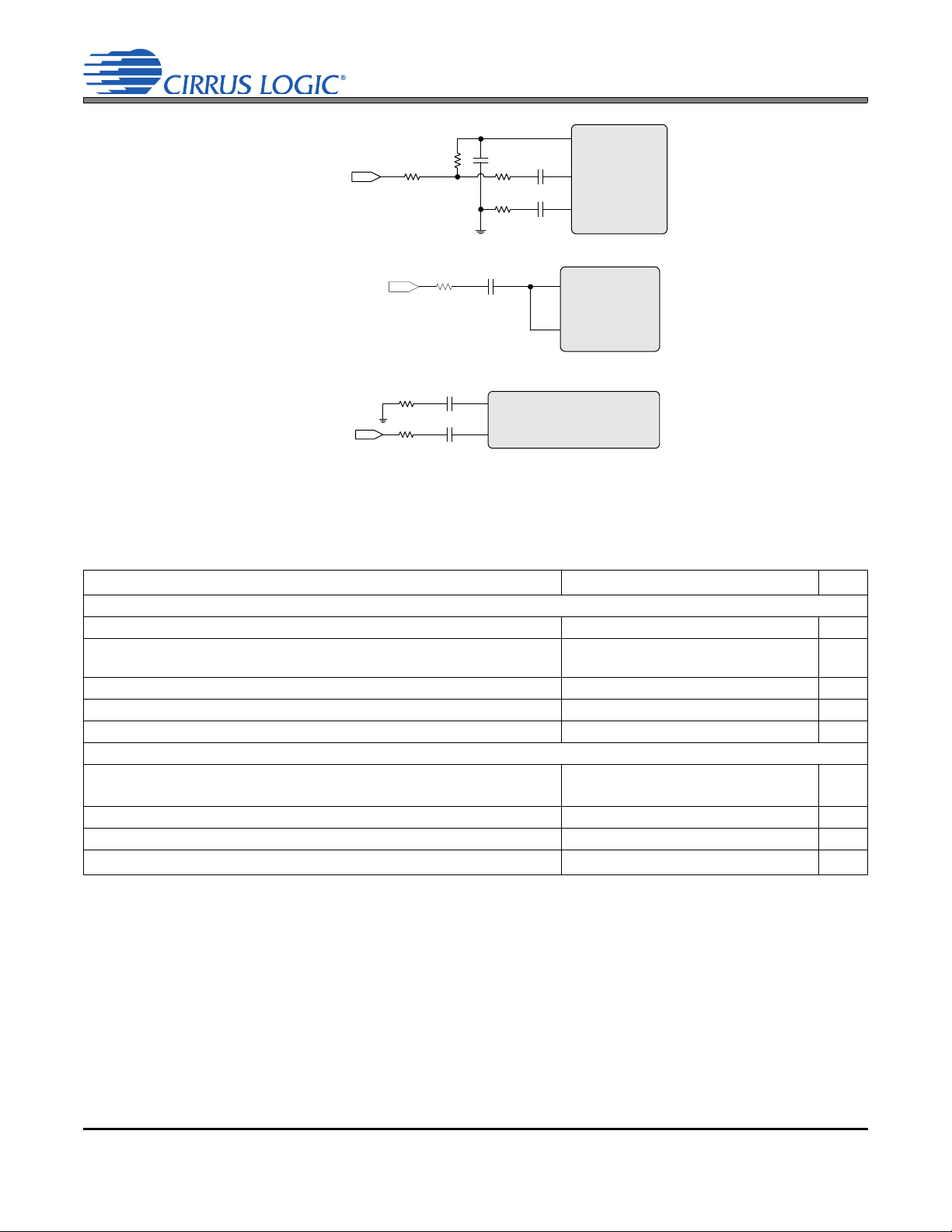
STEREO-ADC AND DUAL-DIGITAL-MIC DIGITAL FILTER
-60 dBFS,
1 kHz
0.1 µF
MICx
MICx_REF
100
MICx_BIAS
2.21 k
0.1 µF
100
2.21 k
1.0 µF
Figure 2. MICx Dynamic Range Test Configuration
100 mVPP,
25 Hz
100
1 F
LINEINx or
MICy
LINEINx_REF
or MICy_REF
Figure 3. Analog Input CMRR Test Setup
0.1 µF
LINEINx or MICx
LINEIN_REF or MICx_REF
100
300 mV
PP,
1 kHz
0.1 µF
100
Figure 4. LINEIN_REF/MICx_REF Input Voltage Test Setup
CHARACTERISTICS
Test Conditions (unless otherwise specified): Fs = 48 kHz (Note 10), f
DMIC_SCLK
= 3.072 MHz (Note 19).
CS42L73
Parameters (Note 2) Min Typ Max Units
Low-Pass Filter Characteristics (Note 20)
Frequency Response (20 Hz to 20 kHz)
Passband to -0.05 dB corner
to -3.0 dB corner
Stopband (Note 21)
Stopband Attenuation
Total Input Path Digital Filter Group Delay
-0.07 - +0.02 dB
-
-
0.41
0.49
-
-
0.60 - - Fs
33 - - dB
- 4.3/Fs - s
High-Pass Filter Characteristics (Note 20) (Note 22)
Passband to -3.0 dB corner
to -0.05 dB corner
Passband Ripple
Phase Deviation @ 20 Hz
Filter Settling Time (input signal goes to 95% of its final value)
-
-
4.10x10
3.57x10
-5
-4
- - 0.01 dB
-5.30-Deg
3
- 12.2x10
/Fs - s
-
-
Notes:
19. Refer to section “Digital Microphone (DMIC) Interface” on page 60 for a description of how the digital mic shift clock
frequency (f
DMIC_SCLK
20. Responses are clock-dependent and will scale with Fs. Note that the response plots (Figures 48 to 52 on pages 127 and
128) have been normalized to Fs and can be denormalized by multiplying the X-axis scale by Fs.
21. Measurement Bandwidth is from Stopband to 3 Fs.
22. High-pass filter is applied after low-pass filter.
) relates to the CS42L73‘s internal master clock rate.
Fs
Fs
Fs
Fs
24 DS882F1
Page 25
CS42L73
THERMAL OVERLOAD DETECT CHARACTERISTICS
Test Conditions: Connections to the CS42L73 are shown in the “Typical Connection Diagram” on page 17; GND = AGND =
PGND = CPGND = DGND = 0 V; all voltages are with respect to ground (GND); VA = 1.80 V.
Parameters Min Typ Max Units
Thermal Overload Detect Threshold Characteristics
Threshold Junction Temperature (T
) (Note 23) THMOVLD_THLD[1:0] = 00b
J
THMOVLD_THLD[1:0] = 01b
THMOVLD_THLD[1:0] = 10b
THMOVLD_THLD[1:0] = 11b
-
-
-
-
150
132
115
98
-
-
-
-
°C
°C
°C
°C
Notes:
23. The thermal overload detect threshold temperature level can vary from the nominal value by ±10 °C.
ASRC DIGITAL FILTER CHARACTERISTICS
Test Conditions (unless otherwise specified): Fs = 48 kHz (Note 10); Fs
Parameters (Note 2) (Note 25) Min Typ Max Units
Low-Pass Filter Characteristics (Note 24)
Frequency Response (0 Hz to 20 kHz)
Passband to -0.05 dB corner
to -3.0 dB corner
Stopband
Stopband Attenuation
Total ASRC Group Delay
= 48 kHz (Note 24).
ext
-0.07 - +0.04 dB
-
-
0.55 - - Fs
125 - - dB
- (Note 26) -s
0.48
0.50
-
-
Fs
ext
ext
Notes:
24. Fs
25. Refer to Response plots in Figures 53 and 54 on page 129.
26. The equations for the group delay through the sample rate converters are:
is the sample rate of the serial port (XSP, ASP, or VSP) interface.
ext
• Input (from the serial ports to the core): 6.9/Fs
• Output (from the core to the serial ports): 2.6/Fs
A plot of ASRC group delay values for the extreme supported internal sample rates (Fs) and standard audio sample
rates is found in section “Group Delay” on page 130.
+ 3.0/Fs
ext
+ 14.1/Fs.
ext
DS882F1 25
Page 26
CS42L73
MIC BIAS CHARACTERISTICS
Test Conditions (unless otherwise specified): Connections to the CS42L73 are shown in the “Typical Connection Diagram” on
page 17; GND = AGND = PGND = CPGND = DGND = 0 V; all voltages are with respect to ground (GND); VA = 1.80 V, VP =
3.70 V; TA = +25 C; I
MIC1_BIAS and MIC2_BIAS Characteristics
Output Voltage (Note 27) MIC_BIAS_CTRL = 0b
DC Output Current (I
(Note 28) Total for both outputs
Output Resistance (R
Dropout Voltage (Note 29)
= 500 A; only one bias output is powered up at a time; VP_MIN = 1b, MIC_BIAS_CTRL = 1b.
OUT
Parameters (Note 2) Min Typ Max Units
MIC_BIAS_CTRL = 1b
) Per output
OUT
)
OUT
1.85
2.59
-
-
-35-
- - 340 mV
2.00
2.75
-
-
2.15
2.89
3.0
5.0
V
V
mA
mA
PSRR with 100 mV
PSRR with 100 mV
VP_MIN = 0b, VP = 3.10 V (Note 3) 217 Hz
PSRR with 1 V
VP_MIN = 1b, VP = 3.70 V 217 Hz
signal AC-coupled to VA supply
PP
signal AC-coupled to VP supply
PP
signal AC-coupled to VP supply
PP
217 Hz
1 kHz
20 kHz
1 kHz
20 kHz
1 kHz
20 kHz
-
-
-
-
-
-
-
-
-
105
100
90
90
90
70
110
105
90
-
-
-
-
-
-
-
-
-
Notes:
27. The output voltage includes attenuation due to the Mic Bias Output Resistance (R
28. Specifies use limits for the normal operation and MIC2 short conditions.
29. Dropout Voltage indicates the point where an output’s voltage starts to vary significantly with reductions to its supply
voltage. When the VP supply voltage drops below the programmed MIC2_BIAS output voltage plus the Dropout Voltage, the MIC2_BIAS output voltage will progressively decrease as its supply decreases. Dropout Voltage is measured
by reducing the VP supply until MIC2_BIAS drops 10 mV from its initial voltage with the default typical test condition VP
voltage (= 3.80 V from table heading above). The difference between the VP supply voltage and the MIC2_BIAS voltage
at this point is the dropout voltage. For instance, if the initial MIC2_BIAS output is 2.86 V when VP = 3.80 V and VP =
3.19 V when MIC2_BIAS drops to 2.85 V (-10mV), the Dropout Voltage is 340 mV (3.19 V – 2.85 V).
OUT
).
dB
dB
dB
dB
dB
dB
dB
dB
dB
26 DS882F1
Page 27
CS42L73
SERIAL PORT TO STEREO HP OUTPUT CHARACTERISTICS
Test conditions (unless otherwise specified): “Typical Connection Diagram” on page 17 shows CS42L73 connections (including
Zobel Networks on outputs); Input test signal is a 24-bit full-scale 997-Hz sine wave with 1 LSB of triangular PDF dither applied;
GND = AGND = PGND = CPGND = DGND = 0 V; all voltages are with respect to ground (GND); VA = VCP = 1.80 V; T
C; VCP Mode; Measurement Bandwidth is 20 Hz to 20 kHz; Fs = 48 kHz (Note 10); ASP is used and is in slave mode with Fs
= 48 kHz; test loading is configured as per Figure 5 on page 28 (R
and CL(= C
L
) as indicated in the table below); Mixer
L(Max)
Attenuation and Digital Volume = 0 dB, Digital and Analog Mutes are disabled.
Parameters (Note 2) Min Typ Max Units
Load RL = 16 (Analog Gain = -4 dB) (Note 30)
Dynamic Range
18 to 24-Bit A-weighted
unweighted
16-Bit A-weighted
unweighted
Total Harmonic Distortion + Noise (Note 31) (Note 32) 0 dBFS
Full-scale Output Voltage (Note 32)
Output Power (Full-scale, Per Channel) (P
) (Note 32)
OUT
2 Channels Driven, THD+N -60 dB (0.1%) Analog Vol. = -4 dB, Dig. Vol. = 0 dB
2 Channels Driven, THD+N -40 dB (1%) Analog Vol. = -3 dB, Dig. Vol. = 0 dB
2 Channels Driven, THD+N -20 dB (10%) Analog Vol. = -1 dB, Dig. Vol. = 0 dB
1 Channel Driven, THD+N -60 dB (0.1%) Analog Vol. = -2 dB, Dig. Vol. = 0 dB
1 Channel Driven, THD+N -40 dB (1%) Analog Vol. = -1 dB, Dig. Vol. = 0 dB
1 Channel Driven, THD+N -20 dB (10%) Analog Vol. = +1 dB, Dig. Vol. = 0 dB
Load R
= 32 (Analog Gain = -4 dB) (Note 30)
L
Dynamic Range
18 to 24-Bit A-weighted
unweighted
16-Bit A-weighted
unweighted
Total Harmonic Distortion + Noise (Note 31) (Note 32) 0 dBFS
Full-scale Output Voltage (Note 32)
Output Power (Full-scale, Per Channel) (P
) (Note 32)
OUT
2 Channels Driven, THD+N -75 dB (0.018%) Analog Vol. = -4 dB, Dig. Vol. = 0 dB
2 Channels Driven, THD+N -60 dB (0.1%) Analog Vol. = -1 dB, Dig. Vol. = 0 dB
2 Channels Driven, THD+N -40 dB (1%) Analog Vol. = 0 dB, Dig. Vol. = -0.5 dB
2 Channels Driven, THD+N -20 dB (10%) Analog Vol. = +2 dB, Dig. Vol. = -0.5 dB
1 Channel Driven, THD+N -75 dB (0.018%) Analog Vol. = 0 dB, Dig. Vol. = 0 dB
1 Channel Driven, THD+N -60 dB (0.1%) Analog Vol. = +1 dB, Dig. Vol. = -0.5 dB
1 Channel Driven, THD+N -40 dB (1%) Analog Vol. = +1 dB, Dig. Vol. = 0 dB
1 Channel Driven, THD+N -20 dB (10%) Analog Vol. = +3 dB, Dig. Vol. = -0.5 dB
Load R
= 3 k (Analog Gain = +2 dB) (Note 30)
L
Dynamic Range
18 to 24-Bit A-weighted
unweighted
16-Bit A-weighted
unweighted
Total Harmonic Distortion + Noise (Note 31) (Note 32)
18 to 24-Bit 0 dBFS
-20 dBFS
-60 dBFS
16-Bit 0 dBFS
-20 dBFS
-60 dBFS
87
84
85
82
--70-60dB
0.73•VA 0.79•VA 0.85•VA V
-
-
-
-
-
-
88
85
86
83
93
90
91
88
16
20
27
25
32
44
94
91
92
89
--81-75dB
0.74•VA 0.80•VA 0.86•VA V
-
-
-
-
-
-
-
-
90
87
88
85
-
-
-
-
-
-
8.1
16
17
25
20
23
25
35
96
93
94
91
-85
-73
-33
-83
-71
-31
-
-
-
-
-
-
-
-
-
-
-
-
-
-
-
-
-
-
-
-
-
-
-
-
-
-
-79
-
-27
-77
-
-25
= +25
A
dB
dB
dB
dB
PP
mW
mW
mW
mW
mW
mW
dB
dB
dB
dB
PP
mW
mW
mW
mW
mW
mW
mW
mW
dB
dB
dB
dB
dB
dB
dB
dB
dB
dB
ext
DS882F1 27
Page 28
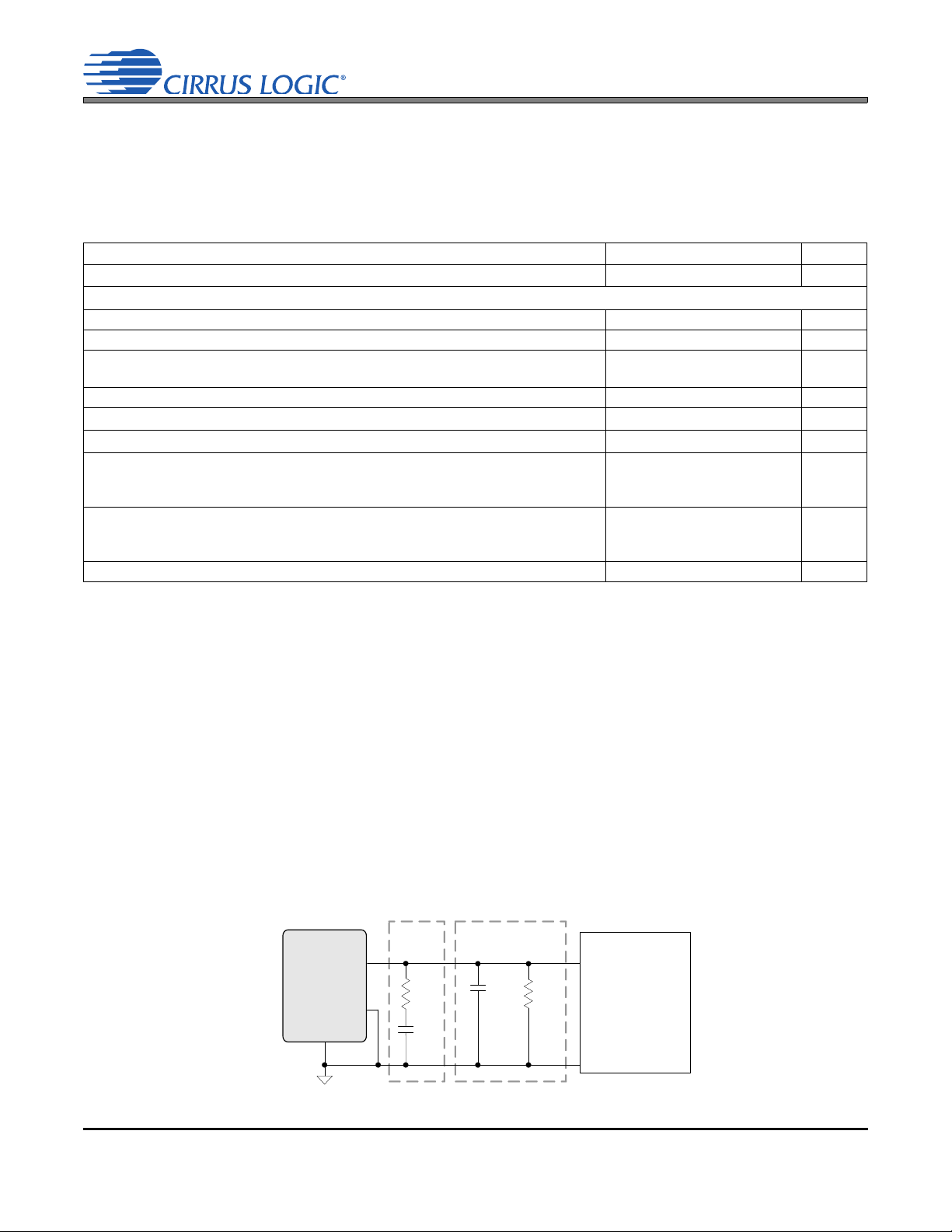
CS42L73
Zobel
Network
Test Load
HPOUTx
CPGND/AGND
C
L
33 nF
100
HPOUT_REF
R
L
Measurement
Device
-
+
Figure 5. Headphone Output Test Configuration
SERIAL PORT TO STEREO HP OUTPUT CHARACTERISTICS (CONTINUED)
Test conditions (unless otherwise specified): “Typical Connection Diagram” on page 17 shows CS42L73 connections (including
Zobel Networks on outputs); Input test signal is a 24-bit full-scale 997-Hz sine wave with 1 LSB of triangular PDF dither applied;
GND = AGND = PGND = CPGND = DGND = 0 V; all voltages are with respect to ground (GND); VA = VCP = 1.80 V; T
C; VCP Mode; Measurement Bandwidth is 20 Hz to 20 kHz; Fs = 48 kHz (Note 10); ASP is used and is in slave mode with Fs
= 48 kHz; test loading is configured as per Figure 5 on page 28 (R
and CL(= C
L
) as indicated in the table below); Mixer
L(Max)
Attenuation and Digital Volume = 0 dB, Digital and Analog Mutes are disabled.
Parameters (Note 2) Min Typ Max Units
Full-scale Output Voltage (Note 32)
Other Characteristics for RL = 16
, 32
or 3 k(Note 33)
Interchannel Isolation (Note 34)
Interchannel Gain Mismatch (Note 34)
Output Offset Voltage (DAC to HPOUTx) Analog mute enabled
0 dB analog gain
Gain Drift
Load Resistance (R
Load Capacitance (C
PSRR with 100 mV
) (Note 35)
L
) (Note 35)
L
signal AC-coupled to VA supply 217 Hz
PP
- Analog Gain = 0 dB; Input test signal held low (all zeros data) 1 kHz
(Note 8) (Note 36) 20 kHz
PSRR with 100 mV
signal AC-coupled to VCP supply 217 Hz
PP
- Analog Gain = 0 dB; Input test signal held low (all zeros data) 1 kHz
(Note 8) (Note 36) 20 kHz
Output Impedance High-Impedance Mode (Note 37)
1.56•VA 1.64•VA 1.73•VA V
-90-dB
- ±0.1 ±0.25 dB
-
-
±0.1
±0.3
±1.0
±2.0
- ±100 - ppm/°C
16 - -
- - 150 pF
-
-
-
-
-
-
75
75
70
85
85
70
-
-
-
-
-
-
3.0 3.14 - k
= +25
A
PP
mV
mV
dB
dB
dB
dB
dB
dB
ext
Notes:
30. Analog Gain setting (refer to “Headphone x Analog Volume Control” on page 103 or “Line Output x Analog Volume Con-
trol” on page 104) must be configured as indicated to achieve specified output characteristics.
31. If the VCP supply level is less than the VA supply level, clipping may occur as the audio signal is handed from the VA
to the VCP powered circuits in the output amplifier. This clipping would occur as the audio signal approaches full-scale,
maximum power output and could prevent achievement of THD+N performance.
32. Full-scale output voltage and power are determined by analog gain settings. Full-scale output voltage values here refer
to the maximum voltage difference achievable on the analog output pins, measured between the HPOUTx/LINEOUTx
and HPOUT_REF/LINEO_REF pins. Modifying internal gain settings to increase peak-to-peak voltage may cause analog output signal clipping, degrading THD+N performance.
33. Unless otherwise specified, measurement is taken for each load resistance test case with the gain set as indicated for
the dynamic range, etc., performance specifications at the given load resistances.
34. Measured between stereo pairs (HPOUTA to HPOUTB or LINEOUTA to LINEOUTB).
35. Figure 5 on page 28 and Figure 6 on page 29 shows headphone and line output test configurations.
36. Valid with the recommended capacitor values on FILT+ and ANA_VQ. Increasing capacitance on FILT+ and ANA_VQ
increases the PSRR at low frequencies.
37. High-impedance state enabled as described in Section 4.18.
28 DS882F1
Page 29
CS42L73
Test Load
LINEOUTx
CPGND/AGND
C
L
LINEO_REF
R
L
Measurement
Device
-
+
Figure 6. Line Output Test Configuration
SERIAL PORT TO STEREO LINE OUTPUT CHARACTERISTICS
Test conditions (unless otherwise specified): Connections to the CS42L73 are shown in the “Typical Connection Diagram” on
page 17; Input test signal is a 24-bit full-scale 997 Hz sine wave with 1 LSB of triangular PDF dither applied; GND = AGND =
PGND = CPGND = DGND = 0 V; all voltages are with respect to ground (GND); VA = VCP = 1.80 V; T
Measurement Bandwidth is 20 Hz to 20 kHz; Fs = 48 kHz (Note 10); ASP is used and is in slave mode with Fs
loading is configured as per Figure 6 on page 29 (R
and CL as indicated in the table below for R
L
L(Min)
uation and Digital Volume = 0 dB, Analog Gain = +2 dB; Digital and Analog Mutes are disabled.
Parameters (Note 2) Min Typ Max Units
(Analog Gain = +2 dB) (Note 30)
Dynamic Range
18 to 24-Bit A-weighted
unweighted
16-Bit A-weighted
unweighted
Total Harmonic Distortion + Noise (Note 31) (Note 32)
18 to 24-Bit 0 dBFS
-20 dBFS
-60 dBFS
16-Bit 0 dBFS
-20 dBFS
-60 dBFS
Full-scale Output Voltage (Note 32) (Note 38)
Other Characteristics
Interchannel Isolation (Note 34)
Interchannel Gain Mismatch (Note 34)
Output Offset Voltage (DAC to LINEOUTx) Analog mute enabled
0 dB analog gain
Gain Drift
Output Resistance (R
Load Resistance (R
Load Capacitances (C
PSRR with 100 mV
)
OUT
) (Note 35)
L
) (Note 35)
L
signal AC-coupled to VA supply 217 Hz
PP
- Analog Gain = 0 dB; Input test signal held low (all zeros data) 1 kHz
(Note 8) (Note 36) 20 kHz
PSRR with 100 mV
signal AC-coupled to VCP supply 217 Hz
PP
- Analog Gain = 0 dB; Input test signal held low (all zeros data) 1 kHz
(Note 8) (Note 36) 20 kHz
91
88
88
85
-
-
-
-
-
-
1.50•VA 1.58•VA 1.66•VA V
-90-dB
- ±0.1 ±0.25 dB
-
-
-±100-ppm/°C
-100-
3--k
--150pF
-
-
-
-
-
-
= +25 C; VCP Mode;
A
and C
97
94
94
91
-86
-74
-34
-84
-71
-31
±0.1
±0.3
70
70
70
85
85
65
= 48 kHz; test
ext
L(Max)
-
-
-
-
-80
-
-28
-78
-
-25
±0.5
±1.0
-
-
-
-
-
-
); Mixer Atten-
dB
dB
dB
dB
dB
dB
dB
dB
dB
dB
PP
mV
mV
dB
dB
dB
dB
dB
dB
Notes:
38. The full-scale output voltage includes attenuation due to the Stereo Line Output Resistance (R
DS882F1 29
OUT
).
Page 30
CS42L73
Test Load
EAROUT+
AGND
R
L
EAROUT-
C
L2
C
L2
C
L1
Measurement
Device
-
+
Figure 7. Ear Speaker Output Test Configuration
SERIAL PORT TO MONO EAR SPEAKER OUTPUT CHARACTERISTICS
Test conditions (unless otherwise specified): Connections to the CS42L73 are shown in the “Typical Connection Diagram” on
page 17; Input test signal is a 24-bit full-scale 997 Hz sine wave with 1 LSB of triangular PDF dither applied; GND = AGND =
PGND = CPGND = DGND = 0 V; all voltages are with respect to ground (GND); VA = 1.80 V; TA = +25 C; Measurement Bandwidth is 20 Hz to 20 kHz; Fs = 48 kHz (Note 10); ASP is used and is in slave mode with Fs
as per Figure 7 on page 30 (R
, CL1, and CL2 as indicated in the table below for R
L
L(Min)
tion = 0 dB, Digital Volume = -2.5 dB, Digital Mute is disabled.
Parameters (Note 2) Min Typ Max Units
Dynamic Range
16 to 24-Bit A-weighted
unweighted
Total Harmonic Distortion + Noise (Note 39), 16 to 24-Bit
0 dBFS, P
Full-scale Output Voltage (Note 39) (Diff. EAROUT ±, see Note 40)
Output Power (Full-scale) (P
) (Note 39)
OUT
THD+N -65 dB (0.056%) Dig. Vol. = -2.5 dB
THD+N -60 dB (0.1%) Dig. Vol. = -2.0 dB
THD+N -40 dB (1%) Dig. Vol. = -1.5 dB
THD+N -20 dB (10%) Dig. Vol. = -0.5 dB
Other Characteristics
Output Offset Voltage (DC offset of diff. EAROUT ±, see Note 40)
Gain Drift
Load Resistance (R
Load Capacitances C
(Note 41) C
PSRR with 100 mV
) (Note 41)
L
L1
from each output to ground
L2
signal AC-coupled to VA supply 217 Hz
PP
- Input test signal held low (all zeros data) 1 kHz
(Note 36) 20 kHz
= 45 mW
OUT
across outputs
= 48 kHz; test loading is configured
ext
, C
82
79
L1(Max)
, and C
88
85
); Mixer Attenua-
L2(Max)
-
-
dB
dB
--70-65dB
1.24•VA 1.34•VA 1.44•VA V
-
-
-
-
45
51
56
66
-
-
-
-
PP
mW
mW
mW
mW
-±2.5±4.0mV
- ±100 - ppm/°C
16 - -
-
-
-
-
-
70
70
70
-
-
150
50
-
-
-
pF
pF
dB
dB
dB
Notes:
39. Modifying internal gain settings to achieve a higher peak-to-peak voltage may result in clipping the analog output signal,
degrading the THD+N performance.
40. Differential peak-to-peak voltage is measured from the extremes (peaks) of the waveform that represents the difference
between the positive and negative signals of the differential pair [i.e. the voltage between the maximum and minimum
(= V+ – V-)].
of V
41. Refer to Figure 7 on page 30 and Figure 8 on page 32 to observe Ear-Speaker, Speakerphone, and Speakerphone
30 DS882F1
Diff
Line-Output test configurations.
Page 31
CS42L73
SERIAL PORT-TO-MONO SPEAKERPHONE OUTPUT CHARACTERISTICS
Test conditions (unless otherwise specified): “Typical Connection Diagram” on page 17 shows CS42L73 connections; Input test
signal is a 24-bit full-scale 997 Hz sine wave with 1 LSB of triangular PDF dither applied; GND = AGND = PGND = CPGND =
DGND = 0 V; all voltages are with respect to ground (GND); VA = 1.80 V, VP = 3.70 V; TA = +25 C; Measurement Bandwidth is
20 Hz to 20 kHz; Fs = 48 kHz (Note 10); ASP is used and is in slave mode with Fs
Figure 8 on page 32 (R
, C
(= C
L
L1
L1(Max)
) and CL2 (= C
) as indicated in the table below); Mixer Attenuation = 0 dB, Digital
L2(Max)
Volume = -5.5 dB, Digital Mute is disabled, SPK_LITE_LOAD = 0b and 1b for R
Parameters (Note 2) Min Typ Max Units
Load RL = 8 (SPK_LITE_LOAD = 0)
Dynamic Range
16 to 24-Bit A-weighted
unweighted
Total Harmonic Distortion + Noise (Note 39) (Note 42), 16- to 24-Bit
0 dBFS, P
Full-scale Output Voltage (Note 39) (Diff. SPKOUT ±, see Note 40)
Output Power (P
THD+N -62 dB (0.079%) VP = 3.70 V, Dig. Vol. = -5.5 dB
THD+N -40 dB (1.0%) VP = 3.70 V, Dig. Vol. = -4.5 dB
THD+N -20 dB (10%) VP = 3.70 V, Dig. Vol. = -2.5 dB
Load RL = 50 k(SPK_LITE_LOAD = 1)
Dynamic Range
16 to 24-Bit A-weighted
Total Harmonic Distortion + Noise (Note 39) (Note 42) 16 to 24-Bit 0 dBFS
Full-scale Output Voltage (Note 39) (Diff. SPKOUT ±, see Note 40)
Other Characteristics for RL = 8 or 50 k(Note 33)
Output Offset Voltage (DC offset of diff. SPKOUT ±, see Note 40)
Gain Drift
Load Resistance (R
Load Capacitances C
(Note 41) (Note 43) C
PSRR with 100 mV
- Input test signal held low (all zeros data) 1 kHz
(Note 36) 20 kHz
PSRR with 100 mV
- Input test signal held low (all zeros data) 1 kHz
(Note 44) 20 kHz
OUT
= 0.48 W
) (Continuous Average) (Note 39)
OUT
VP = 4.20 V, Dig. Vol. = -3.5 dB
VP = 5.00 V, Dig. Vol. = -2.0 dB
VP = 4.20 V, Dig. Vol. = -1.5 dB
VP = 5.00 V, Dig. Vol. = 0.0 dB
) (Note 41) SPK_LITE_LOAD = 0b
L
SPK_LITE_LOAD = 1b
across outputs/load
L1
from each output to ground
L2
signal AC-coupled to VA supply 217 Hz
PP
signal AC-coupled to VP supply 217 Hz
PP
unweighted
= 48 kHz; test loading is configured as per
ext
= 8 and 50 krespectively.
L
80
77
-
-
86
83
-65
0.056
-
-
-62
0.079
2.85•VA 3.09•VA 3.33•VA V
-
-
-
-
-
-
-
78
75
0.48
0.59
0.76
1.06
0.75
0.95
1.36
84
81
-
-
-
-
-
-
-
-
-
--65-60dB
2.99•VA 3.23•VA 3.47•VA V
-±5.0±10.0mV
-±100-ppm/°C
6.5
3.0
-
-
-
-
-
-
-
-
50
70
70
70
70
80
60
8
100
-
-
-
150
50
-
-
-
-
-
-
dB
dB
dB
%
PP
W
W
W
W
W
W
W
dB
dB
PP
k
pF
pF
dB
dB
dB
dB
dB
dB
Notes:
42. When the VP supply level is low and the VA supply level is high, clipping may occur as the audio signal is handed off
from the VA to the VP powered circuits within the output amplifier. This clipping would occur as the audio signal approached full-scale, maximum power output and could result in the specified THD+N performance not being achieved.
43. The maximum speakerphone capacitance across the load is specified as C
. If more load capacitance is desired, con-
L1
tact Cirrus Logic for alternatives using additional external circuitry.
44. Valid with the recommended capacitor values on FILT+ and SPK_VQ. Increasing the capacitance on FILT+ and SPK_
VQ will increase the PSRR at low frequencies.
DS882F1 31
Page 32

CS42L73
Test Load
SPKOUT+
or SPKLINEO+
PGND/AGND
R
L
SPKOUT-
or SPKLINEO-
C
L2
C
L2
C
L1
Measurement
Device
-
+
Figure 8. Speakerphone and Speakerphone Line Output Test Configuration
SERIAL PORT TO MONO SPEAKERPHONE LINE OUTPUT CHARACTERISTICS
Test conditions (unless otherwise specified): Connections to the CS42L73 are shown in the “Typical Connection Diagram” on
page 17; Input test signal is a 24-bit full-scale 997-Hz sine wave with 1 LSB of triangular PDF dither applied; GND = AGND =
PGND = CPGND = DGND = 0 V; all voltages are with respect to ground (GND); VA = 1.80 V, VP = 3.70 V; TA = +25 C; Measurement Bandwidth is 20 Hz to 20 kHz; Fs = 48 kHz (Note 10); ASP is used and is in slave mode with Fs
ing is configured as per Figure 8 on page 32 (R
C
); Mixer Attenuation = 0 dB, Digital Mute is disabled.
L2(Max)
, CL1, and CL2 as indicated in the table below for R
L
L(Typ)
= 48 kHz; test load-
ext
, C
L1(Max)
, and
Parameters (Note 2) Min Typ Max Units
Digital Volume = -5.5 dB
Dynamic Range
16 to 24-Bit A-weighted
unweighted
Total Harmonic Distortion + Noise (Note 39) (Note 42), 16 to 24-Bit 0 dBFS
Full-scale Output Voltage (Note 39) (Note 45) (Diff. SPKLINEO±, see Note 40)
78
75
--65-60dB
2.97•VA 3.21•VA 3.45•VA V
84
81
Other Characteristics
Output Offset Voltage (DC offset of diff. SPKLINEO±, see Note 40)
Gain Drift
Output Resistance (R
Load Resistance (R
Load Capacitances C
(Note 41) (Note 43) C
PSRR with 100 mV
) (Note 46)
OUT
) (Note 41)
L
across outputs/load
L1
from each output to ground
L2
signal AC-coupled to VA supply 217 Hz
PP
–Input test signal held low (all zeros data) 1 kHz
(Note 36) 20 kHz
PSRR with 100 mV
signal AC-coupled to VP supply 217 Hz
PP
–Input test signal held low (all zeros data) 1 kHz
(Note 44) 20 kHz
- ±5.0 ±10.0 mV
- ±100 - ppm/°C
- 100 -
350-k
-
-
-
-
-
-
-
-
-
-
70
70
70
70
80
75
Notes:
45. The full-scale output voltage includes attenuation due to the Speakerphone Line Output Resistance (R
46. The specified output resistance is present on each of the SPKLINEO pins.
-
-
150
50
-
-
-
-
-
-
OUT
dB
dB
PP
pF
pF
dB
dB
dB
dB
dB
dB
).
32 DS882F1
Page 33

CS42L73
STEREO/MONO DAC INTERPOLATION AND ON-CHIP DIGITAL/ANALOG FILTER CHARACTERISTICS
Test Conditions (unless otherwise specified): Fs = 48 kHz (Note 10).
Parameters (Note 2), (Note 47) Min Typ Max Units
DAC Low-Pass Filter Characteristics—EAR/HP/LINE
Frequency Response (0.453x10
Passband to -0.05 dB corner
DAC Low-Pass Filter Characteristics—SPK/SPKLINEOUT
Frequency Response (0.453x10
Passband to -0.05 dB corner
DAC Low-Pass Filter Characteristics—All
Stopband @ -60 dB (Note 21)
Total DAC Group Delay
Post-DAC High-Pass Filter Characteristics
Passband to -3.0 dB corner
Passband Ripple
Phase Deviation @ 20 Hz
Filter Settling Time (input signal goes to 95% of its final value)
-3
x Fs to 0.453 x Fs)
-3
x Fs to 0.453 x Fs)
to -3.0 dB corner
to -3.0 dB corner
to -0.05 dB corner
-0.02 - 0.10 dB
-
-
-0.29 - 0.02 dB
-
-
0.55 - - Fs
- 3.8/Fs - s
-
-
- - 0.01 dB
-0.61-Deg
-
0.48
0.50
0.36
0.50
5.2x10
4.4x10
5
10
/Fs
-
-
-
-
-6
-5
-
-
-s
Fs
Fs
Fs
Fs
Fs
Fs
Notes:
47. Responses are clock dependent and scale with Fs. Note that the response plots (Figures 56 to 59 on pages 131 and 132)
have been normalized to Fs and can be denormalized by multiplying the X-axis scale by Fs.
DS882F1 33
Page 34

CS42L73
Note:
The current draw on each CS42L73 power supply
pin, except VP, is derived from the measured voltage drop across a 10- series resistor between
the associated supply source and each voltage
supply pin. Given the larger currents that are possible on the VP supply, an ammeter is used on
that rail.
Voltmeter
-
+
-
+
-
+
Power Supply
Ammeter
VA
AGND/CPGND/
DGND/PGND
VCP
0.1 µF
2.2 µF
VP
4.7 µF 0.1 µF
VL
CS42L73
0.1 µF
DAC
+
-
10
DAC
+
-
10
DAC
+
-
10
Figure 9. Power Consumption Test Configuration
POWER CONSUMPTION
Test conditions (unless otherwise specified): Connections to the CS42L73 are shown in the “Typical Connection Diagram” on
page 17; GND = AGND = PGND = CPGND = DGND = 0 V; all voltages are with respect to ground (GND); VA = VCP = VL =
1.80 V, VP = 3.70 V; T
derived from MCLK1 input (/1) (thus, Fs = 48 kHz); f
= +25 C; RESET pin inactive; f
A
DMIC_SCLK
attached; SCL inactive, SDA held high; XSP and ASP are in I²S slave mode, VSP is in PCM mode, Fs
48 kHz, Fs
(VSP) = 8 kHz; XSP, ASP, and VSP clocks are held low unless port is in use; XSP, ASP, VSP and DMIC data
ext
inputs are held low (all zeros data), XSP, ASP, and VSP data output lines are not driven by other devices in system; no load on
analog outputs except for HP Zobel; PDN, PDN_ADCx, PDN_BIASx, PDN_DMICx, PDN_XSPSDOUT, PDN_XSPSDIN, PDN_
ASPSDOUT, PDN_ASPSDIN, PDN_VSP, PDN_HP, PDN_EAR, PDN_LO, PDN_SPK, PDN_SPKLO, PDN_THMS = 1b; all
other register controls as per defaults; Figure 9 on page 34 describes the current-measuring method.
= 6.144 MHz, MCLK2 is held low; Internal MCLK enabled and
MCLK1
= 1.536 MHz (/4); silence on analog inputs, microphones are not
(XSP and ASP) =
ext
Case/Configuration
1 Reset RESET
2 Standby (PDN = 1b) MCLK1 held low, MCLK from MCLK1, MCLKDIS = 1b
Stereo Play to HP: ASP to HP
3
Stereo Play to HP - 32 load (Note 48): ASP to HP
4
Handset Voice Call (Digital Mic): DMICA to VSP, Mono VSP to EAR
5
Handset Voice Call (Analog Mic): MIC1 to VSP, Mono VSP to EAR
6
Headset Voice Call: MIC2 to VSP, Mono VSP to Stereo HP
7
Headset Voice Call - 32 load (Note 48): MIC2 to VSP, Mono VSP to Stereo HP
8
and MCLK1 held low, PDN* = x, MCLKDIS = x
PDN_ASPSDIN, PDN_HP = 0b
PDN_ASPSDIN, PDN_HP = 0b
PDN_DMICA, PDN_VSP, PDN_EAR = 0b
PDN_BIAS1, PDN_ADCA, PDN_VSP, PDN_EAR = 0b
PDN_BIAS2, PDN_ADCB, PDN_VSP, PDN_HP = 0b
PDN_BIAS2, PDN_ADCB, PDN_VSP, PDN_HP = 0b
Class
Mode
VCP/3
VCP/2
VCP
VCP/3
VCP/2
VCP
VCP/3 1794 112 475 1280
VCP/3 1794 112 1598 1329
Typical Current (A) Total
H
i
VAiVPiVCPiVL
121 4
-
-1417
4
611
468 1029
611 4 556 1029
611 4 913 1029
611 4 1598 1338
611 4 2238 1338
611 4 4255 1338
- 1233 4 1 1232
- 2377 107 1 1160
Notes:
48. In accordance with the JEITA CP-2905B standard, 0.1 mW per channel is delivered to headphone loads via a 1 kHz
sine wave. The popular 32 headphone loading is used.
Power
(W)
18
31
3809
3968
4610
6399
7551
1118 2
4454
6764
6803
8912
34 DS882F1
Page 35

CS42L73
DIGITAL INTERFACE SPECIFICATIONS AND CHARACTERISTICS
Test Conditions (unless otherwise specified): Connections to the CS42L73 are shown in the “Typical Connection Diagram” on
page 17; GND = AGND = PGND = CPGND = DGND = 0 V; all voltages are with respect to ground (GND); VA = VL = 1.80 V, VP
= 3.70 V; T
Input Leakage Current Inputs with pull-up/downs
(Note 49) (Note 50) Inputs without pull-up/downs
Input Capacitance (Note 49)
SDA Pull-up Resistance (Note 51)
Pull-up Resistance (Note 51)
INT
Logic I/Os
High-Level Output Voltage (I
Low-Level Output Voltage All outputs (I
High-Level Input Voltage
Low-Level Input Voltage
MIC2_SDET Input
High-Level Input Voltage
Low-Level Input Voltage
= +25 C.
A
Parameters (Note 2) Symbol Min Max Units
= -100 A)
OH
SDA and INT
(IOL as per R
P(min)
and R
OL
P_I(min)
= 100 A)
) (Note 51)
I
in
-
-
- - 10 pF
R
P
R
P_I
V
OH
V
OL
500 -
2-k
VL – 0.2 - V
-
-
0.70•VL - V
-0.30•VLV
0.55 - V
-0.35V
V
V
V
IH
V
IL
IH-SD
IL-SD
±4000
±800
0.2
0.2•VL
nA
nA
V
V
Notes:
49. Specification is per pin.
50. Specification includes current through internal pull up/down resistors, where applicable (as defined in section “Digital
Pin/Ball I/O Configurations” on page 16).
51. The minimum values of the pull-up resistors R
and specified in “Digital Interface Specifications and Characteristics” on page 35) are determined using the maximum
level of VL, the minimum sink current strength of their respective output, and the maximum low-level output voltage (V
in “Digital Interface Specifications and Characteristics” on page 35). The maximum values of RP and R
termined by the how fast their associated signals must transition (e.g., the lower the value of RP, the faster the I²C bus
will be able to operate for a given bus load capacitance). Refer to “Switching Specifications—Control Port” on page 40
and to the I²C bus specification (see section “References” on page 137) for more details.
and R
P
(as shown in the “Typical Connection Diagram” on page 17
P_I
may be de-
P_I
OL
DS882F1 35
Page 36

CS42L73
Power Supplies
(other than VP)
V
min
GND
Internal supplies stable
V
operating
t
rh(PWR-RH)
t
irs
Control port active
t
pwr-rs
t
rs(RL-PWR)
t
pwr-rs
RESET
t
pwr-rud
t
pwr-rud
t
pwr-rud
t
pwr-rud
1
st
Supply
Up
Last
Supply
Up
1
st
Supply
Down
Last
Supply
Down
Figure 10. Power and Reset Sequencing
SWITCHING SPECIFICATIONS—POWER, RESET, AND MASTER CLOCKS
Test conditions (unless otherwise specified): Connections to the CS42L73 are shown in the “Typical Connection Diagram” on
page 17; GND = AGND = PGND = CPGND = DGND = 0 V; all voltages are with respect to ground (GND); VA = VCP = VL =
1.80 V, VP = 3.70 V; TA = +25 C; Inputs: Logic 0 = GND, Logic 1 = VL.
Parameters (Note 2) Symbol Min Max Units
Power Supplies (Note 52)
Power Supply Ramp Up/Down
Power Supply Ramp Skew
Reset (Note 52)
t
pwr-rud
t
pwr-rs
-
-
100
1
ms
s
RESET low (Logic 0) Pulse Width t
RESET Hold Time After Power Supplies Ramp Up t
RESET
Setup Time Before Power Supplies Ramp Down t
rh(PWR-RH)
rs(RL-PWR)
rlpw
1-ms
1-ms
1-ms
Master Clocks
MCLK1 or MCLK2 Frequency (Note 53)
MCLK1 or MCLK2 Duty Cycle
-
-4555
-
38.5
Notes:
52. Refer to Figure 10 on page 36.
53. Maximum frequency for highest supported nominal rate is indicated. The supported nominal MCLK1/MCLK2 rates and
their associated configurations are found in section “Internal Master Clock Generation” on page 42. Likewise, the sup-
ported nominal serial port sample rates are found in section “Serial Port Sample Rates and Master Mode Settings” on
page 53.
MHz
%
36 DS882F1
Page 37

CS42L73
DMIC_SCLK
DMIC_SD
t
h(CLKR-SD)
t
P
t
r
t
f
t
h(CLKF-SD)
t
s(SD-CLKR)
t
s(SD-CLKF)
V
IH
V
IL
V
90%
V
10%
Figure 11. Digital Mic Interface Timing
SWITCHING SPECIFICATIONS—DIGITAL MIC INTERFACE
Test conditions: Inputs: Logic 0 = GND = DGND = 0 V, Logic 1 = VL; TA = +25 C; C
Parameters (Note 2) Symbol Min Max Units
Output Clock (DMIC_CLK) Frequency
DMIC_CLK Duty Cycle
DMIC_CLK Rise Time (10% to 90% of VL)
DMIC_CLK Fall Time (90% to 10% of VL)
DMIC_SD Setup Time Before DMIC_CLK Rising Edge (Note 55)
DMIC_SD Hold Time After DMIC_CLK Rising Edge (Note 55)
DMIC_SD Setup Time Before DMIC_CLK Falling Edge (Note 55)
DMIC_SD Hold Time After DMIC_CLK Falling Edge (Note 55)
t
s(SD-CLKR)
t
h(CLKR-SD)
t
s(SD-CLKF)
t
h(CLKF-SD)
Notes:
54. The output clock frequency will follow the master clock (MCLK) rate divided down as per the tables in sections “Digital
Microphone (DMIC) Interface” on page 60. Any deviation of the Master Clock source from the nominal supported rates
will be directly imparted to the output clock rate by the same factor (e.g., +100 ppm offset in the frequency of MCLK1/
MCLK2 will become a +100 ppm offset in DMIC_CLK).
55. Data is valid at the high-level input voltage (V
terface Specifications and Characteristics” on page 35.
) and the low-level input voltage (VIL), which are specified in “Digital In-
IH
1/t
LOAD
P
-
t
r
t
f
= 30 pF.
45
10 -
10 -
600 -
-
(Note 54)
55
-22
-10
0-
kHz
%
ns
ns
ns
ns
ns
ps
DS882F1 37
Page 38

CS42L73
t
h(SK-SDO)
//
t
s(SDI-SK)
xSP_LRCK
xSP_SCLK
xSP_SDOUT
xSP_SDIN
t
P
t
h(SK-SDI)
t
s(SDO -SK)
Note:
x = X, A, or V;
= “s” or “m”
t
s(LK-SK)
t
h(SK-LK)
Figure 12. Serial Port Interface Timing—I²S Format
SWITCHING SPECIFICATIONS—SERIAL PORTS—I²S FORMAT
Test conditions: Inputs: Logic 0 = GND = DGND = 0 V, Logic 1 = VL; TA = +25 C; x = X, A, or V; xSP_LRCK, xSP_SCLK, xSP_
SDOUT; C
Slave Mode
Input sample Rate (xSP_LRCK) (Note 24) (Note 53)
xSP_LRCK Duty Cycle
xSP_SCLK Frequency (Note 10)
xSP_SCLK Duty Cycle
xSP_LRCK Setup Time Before xSP_SCLK Rising Edge
xSP_LRCK Hold Time After xSP_SCLK Rising Edge
xSP_SDOUT Setup Time Before xSP_SCLK Rising Edge
xSP_SDOUT Hold Time After xSP_SCLK Rising Edge
xSP_SDIN Setup Time Before xSP_SCLK Rising Edge
xSP_SDIN Hold Time After xSP_SCLK Rising Edge
Master Mode
Output Sample Rate (xSP_LRCK) (Note 24)
xSP_LRCK Duty Cycle
xSP_SCLK Frequency “SCLK MCLK” Mode
xSP_SCLK Duty Cycle
xSP_LRCK Setup Time Before xSP_SCLK Rising Edge
xSP_LRCK Hold Time After xSP_SCLK Rising Edge
xSP_SDOUT Setup Time Before xSP_SCLK Rising Edge
xSP_SDOUT Hold Time After xSP_SCLK Rising Edge
xSP_SDIN Setup Time Before xSP_SCLK Rising Edge
xSP_SDIN Hold Time After xSP_SCLK Rising Edge
LOAD
= 15 pF.
Parameters (Note 2) Symbol Min Max Units
“SCLK = MCLK” Mode
“SCLK = Pre-MCLK” Mode (Note 57)
Fs
ext-s
-
50
-4555
1/t
Ps
- 68•Fs
-4555
t
ss(LK-SK)
t
hs(SK-LK)
t
ss(SDO-SK)
t
hs(SK-SDO)
t
ss(SDI-SK)
t
hs(SK-SDI)
Fs
ext-m
-
1/t
Pm
40 -
20 -
20 -
30 -
20 -
20 -
-
(Note 56)
45
-
-
-
68•Fs
MCLK
12.1
55
-4555
t
sm(LK-SK)
t
hm(SK-LK)
t
sm(SDO-SK)
t
hm(SK-SDO)
t
sm(SDI-SK)
t
hm(SK-SDI)
35 -
20 -
20 -
30 -
20 -
20 -
ext-m
kHz
%
Hz
%
ns
ns
ns
ns
ns
ns
kHz
%
Hz
Hz
MHz
%
ns
ns
ns
ns
ns
ns
Notes:
56. In Master Mode, the output sample rate follows the Master Clock source (MCLK1 or MCLK2) rate divided down per “In-
ternal Master Clock Generation” on page 42 and “Serial Port Sample Rates and Master Mode Settings” on page 53.
Any Master Clock source deviation from the nominal supported rates is directly imparted to the output sample rate by
the same factor (e.g., +100 ppm offset in the MCLK1/MCLK2 frequency becomes a +100 ppm xSP_LRCK offset).
57. Maximum frequency for highest supported nominal rate is indicated. The supported nominal rates are described in section “SCLK = MCLK Modes” on page 53.
38 DS882F1
Page 39

CS42L73
t
hs(SK-SDO)
//
t
ss(SDI-SK)
xSP_LRCK
xSP_SCLK
xSP_SDOUT
xSP_SDIN
t
Ps
t
hs(SK-SDI)
t
ss(SDO-SK)
t
ss(LK-SK)
t
hs(SK-LK)
Note:
x = X, A, or V
Figure 13. Serial Port Interface Timing—PCM Format
SWITCHING SPECIFICATIONS—SERIAL PORTS—PCM FORMAT
Test condition: Inputs: Logic 0 = GND = DGND = 0 V, Logic 1 = VL; TA = +25 C; x = X or V; xSP_LRCK, xSP_SCLK, xSP_
SDOUT; C
Slave Mode
Input Sample Rate (xSP_LRCK) (Note 24) (Note 53)
xSP_LRCK Duty Cycle
xSP_SCLK Frequency (Note 10)
xSP_SCLK Duty Cycle
xSP_LRCK Setup Time Before xSP_SCLK Falling Edge
xSP_LRCK Hold Time After xSP_SCLK Falling Edge
xSP_SDOUT Setup Time Before xSP_SCLK Falling Edge
xSP_SDOUT Hold Time After xSP_SCLK Falling Edge
xSP_SDIN Setup Time Before xSP_SCLK Falling Edge
xSP_SDIN Hold Time After xSP_SCLK Falling Edge
LOAD
= 15 pF.
Parameters (Note 2) Symbol Min Max Units
Fs
ext-s
-
-4555
1/t
Ps
-68•Fs
-4555
t
ss(LK-SK)
t
hs(SK-LK)
t
ss(SDO-SK)
t
hs(SK-SDO)
t
ss(SDI-SK)
t
hs(SK-SDI)
40 -
20 -
20 -
30 -
20 -
20 -
50
kHz
%
Hz
%
ns
ns
ns
ns
ns
ns
DS882F1 39
Page 40

CS42L73
t
buf
t
hdst
t
hdst
t
low
t
r
t
f
t
hdd
t
high
t
sud
t
sust
t
susp
Stop Start
Start
Stop
Repeated
SDA
SCL
t
irs
RESET
Figure 14. I²C Control Port Timing
SWITCHING SPECIFICATIONS—CONTROL PORT
Test conditions: Inputs: Logic 0 = GND = DGND = 0 V, Logic 1 = VL; TA = +25 C; SDA load capacitance equal to maximum
value of Cb specified below (Note 58); minimum SDA pull-up resistance (R
Parameters (Note 2) Symbol Min Max Unit
RESET Rising Edge to Start (Note 52) t
SCL Clock Frequency
Start Condition Hold Time (prior to first clock pulse)
Clock Low time
Clock High Time
Setup Time for Repeated Start Condition
SDA Input Hold Time from SCL Falling (Note 59)
SDA Output Hold Time from SCL Falling
SDA Setup Time to SCL Rising
Rise Time of SCL and SDA
Fall Time SCL and SDA
Setup Time for Stop Condition
Bus Free Time Between Transmissions
SDA Bus Load Capacitance (Note 51)
P(min)
) (Note 51).
irs
f
scl
t
hdst
t
low
t
high
t
sust
t
hddi
t
hddo
t
sud
t
r
t
f
t
susp
t
buf
C
b
500 - ns
- 550 kHz
0.6 - µs
1.3 - µs
0.6 - µs
0.6 - µs
00.9µs
0.2 0.9 µs
100 - ns
- 300 ns
- 300 ns
0.6 - µs
1.3 - µs
- 400 pF
Notes:
58. All specifications are valid for the signals at the pins of the CS42L73 with the specified load capacitance.
59. Data must be held for sufficient time to bridge the transition time, t
, of SCL.
f
40 DS882F1
Page 41

4. APPLICATIONS
4.1 Overview
4.1.1 Basic Architecture
The CS42L73 is a highly integrated, ultralow power, 24-bit audio CODEC comprising a stereo ADC and
two stereo DAC converters. The ADC is fed by pseudodifferential inputs. The DACs feed two stereo pseudodifferential output amplifiers and three mono (or one mono and one stereo, depending on configuration)
full-differential amplifiers. The ADC and DAC are designed using multibit delta-sigma techniques. Both
converters operate at a low oversampling ratio, maximizing power savings while maintaining high performance.
The serial data interface ports of the CS42L73 may operate at standard audio sample rates as either the
master or slave of timing. The timing of the core of the CS42L73 is flexibly sourced, without the need of
a PLL, by clocks with typical audio clock rates (N x 5.6448 or 6.1440 MHz; N = 1 or 2), USB rates (6, 12,
or 24 MHz), or common cell phone reference rates (N x 13.0 or 19.2 MHz; N = 1 or 2).
Designed with a very low voltage digital core and low voltage Class H amplifiers (powered from an integrated LDO regulator and a step-down/inverting charge pump, respectively), the CS42L73 provides significant reduction in overall power consumption.
4.1.2 Line and Microphone Inputs
CS42L73
The analog input portion of the CODEC allows selection from stereo line-level or mic sources. The selected source is fed into a microphone preamplifier (when applicable) and then a PGA, before entering the
stereo ADC.
When used, the pseudodifferential analog input configuration provides noise-rejection for single-ended
analog inputs to the CS42L73.
4.1.3 Line and Headphone Outputs (Class H, Ground-Centered Amplifiers)
The analog output portion of the CODEC includes separate pseudodifferential headphone and line out
Class H amplifiers. An on-chip step-down/inverting charge pump creates a positive and negative voltage
equal to the input, one-half the input, or one-third the input supply for the amplifiers, allowing an adaptable,
full-scale output swing centered around ground. The inverting architecture eliminates the need for large
DC-blocking capacitors and allows the amplifier to deliver more power to headphone loads at lower supply
voltages. The step-down architecture allows the amplifier’s power supply to adapt to the required output
signal. This adaptive power supply scheme converts traditional Class AB amplifiers into more power-efficient Class H amplifiers.
4.1.4 Digital Mixer
The digital mixer facilitates the mixing and routing of the ADC and serial port audio data to the device analog and Serial port outputs. All routes from inputs to outputs are supported.
All paths have selectable attenuation before being mixed to allow relative volume control and to avoid clipping.
4.1.5 Power Management
Several control registers and bits provide independent power down control of the analog and digital sections of the CS42L73, allowing operation in select applications with minimal power consumption.
DS882F1 41
Page 42

4.2 Internal Master Clock Generation
Table 1 outlines the supported internal Master Clock (MCLK) nominal frequencies and how they are derived
from the supported frequencies of the external MCLK sources (MCLK1 and MCLK2).
Table 1. Internal Master Clock Generation
CS42L73
MCLK1/MCLK2
Rate (MHz)
5.6448 1 5.6448 44.100 000
11.2896 2 010
6.0000 1 6.0000 46.875 000
12.0000 2 010
24.0000 4 100
6.1440 1 6.1440 48.000 000
12.2880 2 010
13.0000 2 6.5000 50.781 010
26.0000 4 100
19.2000 3 6.4000 50.000 011
38.4000 6 101
Required Divide
Ratio
Notes:
1. The MCLKDIV[2:0] register control is described in section “Master Clock Divide Ratio” on page 87.
2. To save power, MCLK may be disabled using the MCLKDIS register control (refer to section “Master
Clock Disable” on page 87).
3. Refer to section “SCLK = MCLK Modes” on page 53 for a description of the frequency limitations on
MCLK1 and MCLK2 when using the “SCLK = MCLK” or “SCLK = Pre-MCLK” modes.
4.3 Thermal Overload Notification
The CS42L73 can be configured to notify the system processor when its die temperature is too high. The
processor can use this notification prevent possible damage to the CS42L73 and other devices in the system. When notified, the processor should react by powering down CS42L73 (and/or other devices in the
system) partially or entirely, depending on the extent to which the CS42L73’s power dissipation is the cause
of its excessive die temperature. Note, the Speakerphone output, when used, accounts for the vast majority
of the power dissipation from the CS42L73.
MCLK Rate
(MHz)
Internal Fs
(kHz)
Settings for MCLKDIV[2:0]
(Note 1)
To use thermal overload notification:
1. Enable the thermal sense circuitry by programming PDN_THMS.
2. Configure the threshold temperature (via control bits THMOVLD_THLD[1:0]), over which the Thermal
Overload Interrupt Status bit will be set.
3. If an interrupt is desired when the Thermal Overload Detect (THMOVLD) bit toggles from 0b to 1b, set
the M_THMOVLD control to 1b. If polling is desired, set it to 0b.
4. Monitor (read after interrupt or poll) THMOVLD and react accordingly.
Referenced Control Register Location
PDN_THMS.........................
THMOVLD_THLD[1:0].........
M_THMOVLD ......................
THMOVLD ...........................
“Power Down Thermal Sense” on page 84,
“Thermal Overload Threshold Settings” on page 84
“Interrupt Mask Register 1 (Address 5Eh)” on page 122
“Thermal Overload Detect” on page 122
42 DS882F1
Page 43

4.4 Pseudodifferential Outputs
V
N-LOCAL
V
N-JACK
PGND/DGND/CPGND/AGND
PCB
CS42 L73
JACK
LOAD
≈ V
N-LOC AL
V
N-LOA D
≈ V
N-LOCAL-VN-JACK
HPOUT_REF
LINEO_REF
HPOUTx
LINE OUTx
Figure 15. Single-Ended Output Configuration
V
N-JACK
GNDD/ GNDA/GND CP
PCB
CS42L73
JACK
LOAD
≈ V
N-JACK
V
N-LOAD
≈ 0
HPOUT_REF
LINEO_REF
HPOUTx
LINE OUTA
LINE OUTB
Figure 16. Pseudodifferential Output Configuration
The CS42L73 provides access to the headphone and line output amplifiers’ reference inputs via the
HPOUT_REF and LINEO_REF pins. These pins may be connected to either the ground at the device, or
the ground return pin of each amplifier’s corresponding output connector. By routing HPOUT_REF and
LINEO_REF to the ground at the device, the respective amplifier’s common mode is dictated by the
ground local to the device. An equivalent circuit is shown in Figure 15 where the ground-noise voltages
developed local to the device and the jack are modeled as voltage sources V
spectively. V
N-LOCAL
across the load (V
distances to an output connector, V
nificant and can compromise dynamic range performance.
is transferred to the output of the amplifier. V
). For PCB designs in which the headphone or line output signals traverse long
N-LOAD
N-LOCAL
and V
N-LOCAL
can be different. As such, V
N-JACK
- V
N-LOCAL
N-JACK
CS42L73
and V
is then presented
N-LOAD
may be sig-
N-JACK
, re-
By routing HPOUT_REF and LINEO_REF to the corresponding output connector as shown in Figure 16,
however, the amplifier’s common mode is dictated by the ground local to the jack. This connection is useful in systems for which, as described above, the ground noise local to the device differs from the ground
noise at the jack. As this noise voltage couples to HPOUT_REF and LINEO_REF, it is also transferred
through the amplifier to its output. This behavior allows the ground noise at the jack to be seen as common
mode at the load, and as a result, V
Minimize any impedance from the HPOUT_REF and LINEO_REF pins to the corresponding load ground
(typically the connector ground). Impedance in this path affects analog output attenuation of the output
N-LOAD
amplifier, which affects output offset and step deviation. Table 2 shows the effects of impedance on the
reference pin with regard to output attenuation:
DS882F1 43
is minimized.
Page 44

External Impedance () Maximum Attenuation Possible @ -76 dB Setting (dB)
VCP
+VCPFILT
ADPT PWR[2:0]
+VCP
+VC P /2
Cl ass H Control
Step-down/I nverting
Ch arg e P ump
CHGFREQ[3 :0]
+VC P /3
-VCPF ILT
-VCP
-VC P /2
-VC P /3
Figure 17. Class H Operation
0-76.0
1-74.5
10 -72.3
50 -64.8
100 -60.0
4.5 Class H Amplifier
CS42L73
Table 2. Example of Impedance in Reference Path
Referenced Control Register Location
Analog Output
ADPTPWR[2:0] “Adaptive Power Adjustment” on page 85
The CS42L73 headphone and line output amplifiers use a patent-pending Cirrus Logic Tri-Modal Class H
technology. This technology maximizes operating efficiency of the typical Class AB amplifier while maintaining high performance. In a Class H amplifier design, the rail voltages supplied to the amplifier vary with the
needs of the music passage that is being amplified. This prevents unnecessarily wasting energy during low
power passages of program material or when the program material is played back at a low volume level.
The central component of the Tri-Modal Class H technology found in the CS42L73 is the internal charge
pump, which creates the rail voltages for the headphone and line amplifiers of the device. The charge pump
receives its input voltage from the voltage present on the CS42L73 VCP pin. From this input voltage, the
charge pump creates three sets of the differential rail voltages that are supplied to the amplifier output stages: ±VCP, ±VCP/2, and ±VCP/3.
4.5.1 Power Control Options
The method by which the CS42L73 selects the set of rail voltages supplied to the amplifier output stages
depends on the settings of the ADPTPWR[2:0] bits found in “Charge Pump Frequency and Class H Con-
figuration (Address 09h)” section on page 85. There are five possible settings for these bits: Mode 000,
001, 010, 011, and 111.
Referenced Control Register Location
44 DS882F1
ADPTPWR[2:0].................... “Adaptive Power Adjustment” on page 85
Page 45

CS42L73
HL_PLYBCKB=A
HLxDMUTE
HLxDVOL
Charge Pump
Headphone
Amplifiers
Lineout
Amplifiers
ASPINV
VSPINV
XSPINV
PDN_ HP
HPxAVOL
HPxAMUTE
PDN_L O
LOxAVOL
LOxAMUTE
PDN_ ADC x
PDN _DM I Cx
IPB=A
PGAB = A
PGAxMU X
Headphone
Volume Settings:
Lineout
Volume Settings:
Analog Input
Volume Settings:
ASP/VSP/XSP
Advisory
Volume Settings:
DAC
Volume Settings:
DAC Limiter
ALC
DAC Mixer
HLx_IPx
HL x_XSPx
HL x_ASPx
HL x_VSPM
STRI NV
Stereo Input
Advisory
Volume Settings:
BOOSTx
IPxMUTE
MI C_PREAM Px
PGAxVOL
IPxDVOL
Figure 18. Class H Control - Adapt-to-Volume Mode
4.5.1.1 Standard Class AB Operation (Mode 001, 010, and 011)
When the ADPTPWR is set to 001, 010, or 011, the rail voltages supplied to the amplifiers will be held to
±VCP, ±VCP/2, or ±VCP/3, respectively. For these settings, the rail voltages supplied to the output stages
are held constant, regardless of the signal level, internal volume settings, or the settings of the advisory
volume registers. In these settings, the amplifiers in the CS42L73 simply operate in a traditional Class AB
configuration.
Note: In the 010 or 011 setting, clipping can occur if the input signal level exceeds the headroom of the
output amplifier.
4.5.1.2 Adapt-to-Volume Settings (Mode 000)
If the Adaptive Power bits are set to 000, the CS42L73 determines which set of rail voltages to send to
the amplifiers based upon the gain and attenuation levels of all active internal processing blocks. To adjust
for digital (DSP) input volume settings, it also takes into account the settings of the advisory volume registers. The combined effect of all volume settings is shown in Figure 18.
DS882F1 45
If the total gain and attenuation set in the volume control registers would cause the amplifiers to clip the
signal with the lowest voltage setting (±VCP/3), the control logic instructs the charge pump to provide the
next higher set of the rail voltages (±VCP/2, then ±VCP) to the amplifiers until the signal is no longer
clipped or the charge pump is in its highest mode (±VCP).
Note that the A and B channels of each respective volume control must both cross the threshold to trigger
a change to a lower VCP mode. If either channel crossed the threshold in an upward direction, the charge
pump will switch to a higher VCP mode. The control logic also monitors various functions (listed in the
following table) that may affect the total gain and attenuation of the signal applied to the amplifiers.
Page 46

Referenced Control Register Location
PDN_HP..............................
HPxAVOL ............................
HPxAMUTE .........................
PDN_LO ..............................
LOxAVOL ............................
LOxAMUTE .........................
HL_PLYBCKB=A.................
HLxDMUTE .........................
HLxDVOL ............................
PDN_ADCx .........................
PDN_DMICx........................
IPB=A ..................................
PGAB=A..............................
PGAxMUX ...........................
BOOSTx ..............................
IPxMUTE .............................
MIC_PREAMPx...................
PGAxVOL............................
IPxDVOL .............................
HLx_IPx...............................
HLx_XSPx ...........................
HLx_ASPx ...........................
HLx_VSPM..........................
STRINV ...............................
ASPINV ...............................
VSPINV ...............................
XSPINV ...............................
“Power Down Headphone” on page 85
“Headphone x Analog Volume Control” on page 103
“Headphone x Analog Mute” on page 103
“Power Down Line Output” on page 85
“Line Output x Analog Volume Control” on page 104
“Line Output x Analog Mute” on page 104
“Headphone/Line Output (HL) Playback Channels B=A” on page 100
“Headphone/Line Output (HL) x Digital Mute” on page 101
“Headphone/Line Output (HL) x Digital Volume Control” on page 101
“Power Down ADC x” on page 82
“Power Down Digital Mic x” on page 82
“Input Path Channel B=A” on page 94
“PREAMP and PGA Channel B=A” on page 94
“PGA x Input Select” on page 97
“Boost x” on page 97
“Input Path x Digital Mute” on page 97
“Mic PREAMP x Volume” on page 98
“PGAx Volume” on page 98
“Input Path x Digital Volume Control” on page 99
“Stereo Mixer Input Attenuation” on page 119
“Stereo Mixer Input Attenuation” on page 119
“Stereo Mixer Input Attenuation” on page 119
“Stereo Mixer Input Attenuation” on page 119
“Stereo Input Path Advisory Volume” on page 105
“ASP Input Advisory Volume” on page 106
“VSP Input Advisory Volume” on page 106
“XSP Input Advisory Volume” on page 105
CS42L73
4.5.1.3 Adapt-to-Output Signal (Mode 111)
If the Adaptive Power bits are set to 111, the CS42L73 determines which of the three sets of rail voltages
to send to the amplifiers based solely on the level of the signal being sent to the amplifiers. If that signal
would cause the amplifiers to clip when operating on the lower set of rail voltages, the control logic instructs the charge pump to provide the next higher set of rail voltages to the amplifiers. If that signal would
not cause the amplifiers to clip when operating on the lower set of rail voltages, control logic instructs the
charge pump to provide the lower set of rail voltages to the amplifiers. This mode eliminates the need to
advise the CS42L73 of volume settings external to the device.
4.5.2 Power Supply Transitions
Charge pump transitions from the lower to the higher set of rail voltages occur on the next FLYN/FLYP
clock cycle. Despite the system’s fast response time, the capacitive elements on the VCP_FILT pins prevent the rail voltages from changing instantaneously. Instead, the voltages ramp up from the lower to the
higher supply, based on the time constant created by the output impedance of the charge pump and the
capacitor on the VCP_FILT pin (the transition time is approximately 20 µs). The behavior of ±VCP/2 to
and from ±VCP is shown in Figure 19. During this charging transition, a high dv/dt transient on the inputs
may briefly clip the outputs before the rail voltages charge to the full higher supply level. This transitory
clipping has been found to be inaudible in listening tests.
46 DS882F1
Page 47

CS42L73
+VCP
+VCP
2
Ideal Transition
Actual Transition caused
by +VCP_FILT Capacitor
Time
+VCP
3
-VCP
-VCP
2
-VCP
3
Figure 19. VCP_FILT Transitions
When the charge pump transitions from the higher set of rail voltages to the lower set, there is a 2-second
delay before the charge pump supplies the lower rail voltages to the amplifiers. This hysteresis ensures
that the charge pump does not toggle between the two rail voltages as signals approach the clip threshold.
It also prevents clipping in the instance of repetitive high-level transients in the input signal. The timing
diagram of ±VCP/2 to/from ±VCP for this transitional behavior is detailed in Figure 20.
DS882F1 47
Page 48

CS42L73
Output Level
-15 dB
+VCP
2 seconds
Amplifier Rail
Voltage
Time
Time
+VCP
2
+VCP
3
2 seconds
-VCP
-VCP
2
-VCP
3
-11 dB
Figure 20. VCP_FILT Hysteresis
48 DS882F1
Page 49

4.5.3 Efficiency
0.001 0. 01 0. 1 1 10
0
10
20
30
40
50
60
70
80
90
Power Delivered to Two 30 Loads (mW)
Power Taken From All Supplies (mW)
VCP/ 3 Mode
VCP/ 2 Mode
VCP Mode
Class H Enabled
Figure 21. Input Power vs. Output Power
As discussed in previous sections, the HPOUTx and LINEOUTx amplifiers may operate from one of three
pairs of rail voltages based on the amplitude of the output signal or the relevant volume settings in the
signal path. Figure 21 shows total power drawn by the device vs. power delivered to two headphone loads
when the rails are held constant at each of the three available settings, or when the Class H controller is
set to Adapt-to-Volume mode.
CS42L73
Note: Test Conditions: VCP = VL = VA = 1.8 V, VP = 5 V; MCLK = 6 MHz, LRCK = 44.118 kHz; full-scale
input signal applied through HPOUTA and HPOUTB.
If rail voltages are set to ±VCP Mode, the output amplifiers operate in their least-efficient mode for low-level signals. When rail voltages are held at ±VCP/2 or ±VCP/3, the amplifiers operate in a more efficient
mode, but clip when amplifying a full-scale signal.
The blue trace in Figure 21 shows the benefit of the Tri-Modal Class H design. At lower output levels, the
output of the amplifiers is represented by the ±VCP/3 or ±VCP/2 curves, depending on the signal level.
At higher output levels, the output is represented by the ±VCP curve. The duration in which the amplifiers
operate within any of the three rail pairs (±VCP/3, ±VCP/2, or ±VCP) depends on both the content and
the output level of the program material being amplified. The highest efficiency results from maintaining
an output level that is close to, but does not exceed, the clip threshold of a particular supply curve.
4.6 DAC Limiter
When enabled, the limiter monitors the digital input signal before the DAC modulators, detects when levels
exceed the maximum threshold settings and lowers the volume at a programmable attack rate below the
DS882F1 49
Page 50

CS42L73
LMAXx[2:0]
Output
(after Li miter)
Input
LIMRRATEx[2:0]
LIMARATEx[2:0]
Volume
Limiter
CUSHx[2:0]
ATTA CK/R ELEASE SOUND
CUSHION
LMAXx[2:0]
Figure 22. Peak Detect & Limiter
maximum threshold. When the input signal level falls below the maximum threshold, the AOUT volume returns to its original level set in the HP/LO Volume Control register at a programmable release rate. Attack
and release rates are affected by the DAC soft ramp settings and sample rate, Fs. Limiter soft ramp dependency may be independently enabled/disabled using the LIMSRDIS.
Note that the limiter maintains the output signal between the CUSHSPK, CUSHHL, CUSHESL and LMAXSPK, LMAXHL, LMAXESL thresholds. As the digital input signal level changes, the level-controlled output
may not always be the same, but always falls within the thresholds.
Recommended settings: Best limiting performance may be realized with the fastest attack and slowest release setting with soft ramp enabled in the control registers. The CUSHx bits allow the user to set a threshold slightly below the maximum threshold for hysteresis control—this cushions the sound as the limiter
attacks and releases.
Referenced Control Register Location
Limiter Rates ....................... “Limiter Attack Rate HL” on page 107, “Limiter Release Rate HL” on page 107
Limiter Thresholds............... “Limiter Cushion Threshold HL” on page 108, “Limiter Maximum Threshold HL” on page 108
LIMSRDIS ........................... “Limiter Soft-Ramp Disable” on page 100
Volume Controls.................. “Headphone/Line Output (HL) x Digital Volume Control” on page 101
“Limiter Attack Rate Speakerphone [A]” on page 108, “Limiter Release Rate Speakerphone [A]” on
“Limiter Attack Rate ESL [B]” on page 111, “Limiter Release Rate ESL [B]” on page 111
“Limiter Cushion Threshold Speakerphone [A]” on page 110, “Limiter Maximum Threshold Speaker-
“Limiter Cushion Threshold ESL [B]” on page 112, “Limiter Maximum Threshold ESL [B]” on page 112
“Speakerphone Out [A] Digital Volume Control” on page 102
“Ear Speaker/Speakerphone Line Output (ESL) [B] Digital Volume Control” on page 102
“Speakerphone Out [A] Digital Volume Control” on page 102
page 109
phone [A]” on page 110
50 DS882F1
Page 51

4.7 Analog Output Current Limiter
GND/AGND
R
S
I
VCP
R
S
HPOUTA
HPOUTB
GND/AGND
R
S
I
VCP
R
S
LIN EOU TA
LIN EOU TB
100
100
Figure 23. HP Short Circuit Setup Figure 24. Line Short Circuit Setup
The CS42L73 features built-in current-limit protection for both the headphone and line output amplifiers. The
approximate current through VCP during the short circuit conditions shown in Figure 23 and Figure 24 is
described in Table 3.
Note: 100 is always required in series with the line-output amplifiers. These amplifiers must never be
shorted directly to ground.
While the values in Table 3 show that the device is protected from permanent damage during a short circuit,
they do not represent maximum specification. See “DC Electrical Characteristics” on page 21.
CS42L73
R
Amplifier
HPOUTx
S
()
Maximum Current (mA)
3.3 120
0120
LINEOUTx 0 120
Table 3. Current through VCP with Varying Short Circuits
4.8 Serial Ports
The three independent, highly configurable, serial ports XSP, ASP, and VSP communicate audio and voice
data to and from other devices in the system, such as application processors, Bluetooth transceivers, and
cell-phone modems.
4.8.1 Power Management
The XSP and ASP have separate power-down controls (PDN_XSP_SDOUT, PDN_XSP_SDIN, PDN_
ASP_SDOUT, and PDN_ASP_SDIN) for their input and output data paths. Separating power state controls minimizes power consumption if only monoplex communication is required (e.g., music playback).
The VSP, being targeted for duplex voice communication, has a single power-down control, PDN_VSP.
4.8.2 I/O
Each serial port interface consists to four signals (x = X, A, or V):
• xSP_SCLK Serial data shift clock
• xSP_LRCK Left/right clock
DS882F1 51
• Identifies the start of each serialized data word
• Identifies where each channel (left or right) is located within the data
word when I²S format (refer to section “I²S Format” on page 55) is used
Page 52

CS42L73
CS42L73 x Interface
Transmitting Device #1
Transmitting Device #2
Receiving Device
xSP_SDOUT
xSP_SCLK,
xSP_LRCK
Note:
x = X, A, or V
3ST_xSP
Figure 25. Serial Port Busing when Mastering Timing
CS42L73 x Interface
Transmitting Device #1
Transmitting Device #2
Receiving Device
3ST_xSP
xSP_SDOUT
xSP_SCLK,
xSP_LRCK
Note:
x = X, A, or V
Figure 26. Serial Port Busing When Slave Timed
• Toggles at external sample rate (Fs
• xSP_SDIN Serial data input
• xSP_SDOUT Serial data output
4.8.3 High-impedance Mode
The serial ports may be placed on a clock/data bus that allows multiple masters, without the need for external buffers. The 3ST_XSP, 3ST_ASP, and 3ST_VSP bits place the internal buffers for the respective
serial port interface signals in a high-impedance state, allowing another device to transmit clocks and data
without bus contention. When the CS42L73 serial port is a timing slave, its xSP_SCLK and xSP_LRCK I/
Os are always inputs and are thus unaffected by the 3ST_xSP control.
Figure 25 and Figure 26 show the busing of the serial port interface for both the master and slave timing
CS42L73 serial port use cases.
ext
)
4.8.4 Master and Slave Timing
52 DS882F1
The serial ports can independently operate as either the master of timing or a slave to another device’s
timing. When mastering, xSP_SCLK and xSP_LRCK are outputs, when slaved, they are inputs. Master/
Slave mode is configured by the X_M/S
, A_M/S, and V_M/S bits. Note, master mode is not supported
when the PCM interface format is selected (refer to section “PCM Format” on page 55).
In master mode, the xSP_SCLK and xSP_LRCK clock outputs are derived from either the internal MCLK
(MCLK) or (for a subset of SCLK = MCLK modes, refer to section “SCLK = MCLK Modes” on page 53)
directly from its source, MCLK1 or MCLK2.
When in slave mode, the supported interface sample rates (Fs
in the table “Serial Port Rates and Master Mode Settings” on page 53.
) are as is shown for MCLK = 6.000 MHz
ext
Page 53

CS42L73
The master mode supported rates for each supported MCLK are listed in the aforementioned table. The
table also documents how to program the X_MMCC[5:0], A_MMCC[5:0], and V_MMCC[5:0] registers to
derive the desired master mode Fs
4.8.4.1 SCLK = MCLK Modes
The frequency of the Serial Clock (xSP_SCLK) is programmable in master mode using the register controls X_SCLK = MCLK[1:0], A_SCLK=MCLK[1:0], and V_SCLK = MCLK[1:0]. It can be either automatically derived to approximate 64 cycles per xSP_LRCK period, be equal to MCLK, or it can be set to be
equal to Pre-MCLK, the predivided version of MCLK (MCLK1 or MCLK2 as per register control MCLKSEL).
When in MCLK mode, all the MCLK1/MCLK2 rates and corresponding supported MCLK rates shown in
Table 1. “Internal Master Clock Generation” on page 42 are supported. When in Pre-MCLK mode, the
supported MCLK1/MCLK2 rates are as is shown in the following table.
Table 4. Supported MCLK1/MCLK2 Rates for Pre-MCLK
MCLK1/MCLK2 = xSP_SCLK Rate (MHz)
and how much the derived Fs
ext
5.6448
11.2896
6.0000
12.0000
6.1440
rate deviates from the desired rate.
ext
Mode
4.8.5 Serial Port Sample Rates and Master Mode Settings
Table 5 illustrates the supported serial port nominal audio sample rates (Fs
to generate them when in master mode. See the notes on the following page.
Table 5. Serial Port Rates and Master Mode Settings
MCLK Rate
(MHz) (Note 1)
5.6448
6.0000 22.0500 22.0588
(Note 3) 32.0000 32.0000/31.9149
6.1440
Standard Audio
Sample Rate (kHz)
11.0250 11.0250
22.0500 22.0500
44.1000 44.1000
8.0000 8.0000
11.0250 11.0294
12.0000 12.0000
16.0000 16.0000
24.0000 24.0000
44.1000 44.1176
48.0000 48.0000
8.0000 8.0000
12.0000 12.0000
16.0000 16.0000
24.0000 24.0000
32.0000 32.0000
48.0000 48.0000
Actual Master Mode xSP_
LRCK Rate (Fs
ext)
Deviation (%) Settings for x_
(kHz)
0.00
0.00
0.00
0.00
0.04
0.00
0.00
0.04
0.00
0.00/–0.27
0.04
0.00
0.00
0.00
0.00
0.00
0.00
0.00
) and the settings required
ext
MMCC[5:0] (Note 2)
11 0000
10 0000
01 0000
11 1001
11 0 0 11
11 0001
10 1001
10 0011
10 0001
01 1001
01 0011
01 0001
11 1000
11 0000
10 1000
10 0000
01 1000
01 0000
DS882F1 53
Page 54

Table 5. Serial Port Rates and Master Mode Settings
CS42L73
MCLK Rate
(MHz) (Note 1)
6.5000
6.4000
Standard Audio
Sample Rate (kHz)
8.0000 7.9951
11.0250 11.0169
12.0000 11.9926
16.0000 15.9902
22.0500 22.0339
24.0000 23.9852
32.0000 31.9803
44.1000 44.0678
48.0000 47.9705
8.0000 8.0000
11.0250 11.0345
12.0000 12.0000
16.0000 16.0000
22.0500 22.0690
24.0000 24.0000
32.0000 32.0000
44.1000 44.1379
48.0000 48.0000
Actual Master Mode xSP_
LRCK Rate (Fs
ext)
(kHz)
Deviation (%) Settings for x_
MMCC[5:0] (Note 2)
-0.06
-0.07
-0.06
-0.06
-0.07
-0.06
-0.06
-0.07
-0.06
0.00
0.09
0.00
0.00
0.09
0.00
0.00
0.09
0.00
11 11 0 0
11 0101
11 0100
10 1100
10 0101
10 0100
01 1100
01 0101
01 0100
11 111 0
11 0 111
11 0 11 0
10 1110
10 0111
10 0110
01 1110
01 0111
01 0110
Notes:
1. Refer to section “Internal Master Clock Generation” on page 42.
2. See “XSP Master Mode Clock Control Dividers” on page 89, “ASP Master Mode Clock Control Dividers” on
page 90, and “VSP Master Mode Clock Control Dividers” on page 92 for details regarding MMCC control.
3. For this row, the xSP_LRCK rate and resulting deviation varies based on the programming of MCLKDIV and
x_SCLK=MCLK. The values given, ValueA/ValueB, are applicable according to the rule set in Table 6.
Table 6. Actual xSP_LRCK Rate/Deviation Selector for Note 3
MCLKDIV[2:0] MCLK Divide Ratio x_SCLK=MCLK SCLK=MCLK Mode Applicable Value
xxx x 00b SCLK MCLK ValueA
xxx x 10b SCLK = MCLK ValueB
000 1 11b SCLK = Pre-MCLK ValueB
010 2 11b SCLK = Pre-MCLK ValueA
4.8.6 Formats
Table 7 lists formats supported on the CS42L73 serial ports:
Table 7. Supported Serial Port Formats
Serial Port I²S Format PCM Format
XSP
ASP x
VSP
The XSPDIF and VSPDIF register bits are used to select the format for the XSP and VSP. There is no
selector for the ASP, since it always uses I²S format.
54 DS882F1
Page 55

CS42L73
Figure 27. I²S Format
xSP_LRCK
xSP_SCLK
xSP_SDIN
xSP_SDOUT
MSB MSB-1 LSB+1 LSB
1/Fs
ext
Note:
x = X, A, or V
MSB MSB-1 LSB+1 LSB MSB
xSP_SCLK may
stop or continue
t
extraA =
None to some time
xSP_SCLK may
stop or continue
t
extraB =
None to some time
Left (A) Channel Right (B) Channel
4.8.6.1 I²S Format
Selecting I²S format provides the following behavior:
• Up to 24 bits/sample of stereo data can be transported (see “Data Bit Depths” on page 57)
• Master or Slave timing may be selected
• xSP_LRCK identifies the start of a new sample word and the active stereo channel (A or B)
• Data is clocked into the xSP_SDIN input using the rising edge of xSP_SCLK
• Data is clocked out of the xSP_SDOUT output using the falling edge of xSP_SCLK
• Bit order is MSB to LSB
Refer to section “Mono/Stereo” on page 57 for details on how the stereo nature of the I²S format impacts
the operation of the VSP.
The signaling for I²S format is shown in Figure 27.
4.8.6.2 PCM Format
If PCM format is selected:
• 16 bits/sample of mono data can be transported (refer to “Data Bit Depths” on page 57)
• Slave timing is supported
• xSP_LRCK (aka WA) identifies the start of a new sample word, acting as a Word-Aligner
• Data is clocked into the xSP_SDIN input using the falling edge of xSP_SCLK
• Data is clocked out of the xSP_SDOUT output using the rising edge of xSP_SCLK
• Bit order may selected as MSB-to-LSB or LSB-to-MSB
• The PCM Mode must be selected
PCM Format supports word bit-order reversal (LSB-to-MSB vs. MSB-to-LSB) via the XPCM_BIT_ORDER
and VPCM_BIT_ORDER bits. If enabled, the data in the location (refer to the signaling waveforms in
Figures 28 to 30) normally occupied by the data’s MSB bit is occupied by the data’s LSB bit, the location
normally occupied by the data’s MSB-1 bit is occupied by the data’s LSB+1 bit, and so on.
The X_PCM_MODE[1:0] and V_PCM_MODE[1:0] fields select how WA (xSP_LRCK) may vary in width
and location vs. the data.
Mode 0:
– WA may be one or two xSP_SCLK periods wide
– 1st data bit is transported in the cycle following WA
– No data is sampled into the CS42L73 during WA
– When WA is 2 xSP_SCLK periods wide, the first data bit is output from the CS42L73 for 2 cycles,
during the last active cycle of WA and during the bit that follows WA (as usual)
Section “Mono/Stereo” on page 57 describes how the mono nature of the PCM format affects operation.
Signaling for all PCM format modes, with xPCM_BIT_ORDER = 0b (MSB-to-LSB), are shown in
Figures 28 to 30).
DS882F1 55
Page 56

CS42L73
Figure 28. PCM Format—Mode 0
xSP_LRCK
(WA )
xSP_SCLK
xSP_SDIN
16 bits
xSP_SDOUT
xSP_SCLK may stop or continue,
t
extra
= 0 to N xSP_SCLK periods
MSB M SB-1 MSB-2 MSB-3 LSB +2 LSB+1 LSB MSB
1/Fs
ext
17 xSP_SCLK periods when WA is 1 xSP_SCLK period wide,
18 xSP_SCLK periods when WA is 2 xSP_SCLK periods wide
xSP_LRCK
(WA )
xSP_SCLK
xSP_SDIN
xSP_SDOUT
MSB
t
extra
= 0,
WA is 1 xSP_SCLK period wide,
1/Fs
ext
= 17 xSP_SCLK periods
LSB
xSP_LRCK
(WA )
xSP_SCLK
xSP_SDIN
xSP_SDOUT
MSB
t
extra
= 0,
WA is 2 xSP_SCLK periods wide,
1/Fs
ext
= 18 xSP_SCLK periods
LSB
xSP_LRCK
(WA )
xSP_SCLK
xSP_SDIN
xSP_SDOUT
MSB
t
extra
= 1 xSP_SCLK period,
WA is 1 xSP_SCLK period wide,
1/Fs
ext
= 18 xSP_SCLK periods
LSB
PCM_SCLK ma y
stop or continue
MSB-1 M SB-2 MSB-3 LSB +2 LSB+1 LSB
LSB MSB
MSB MSB MSBMSB
Note:
x = X, A, or V
Figure 29. PCM Format—Mode 1
xSP_LRCK
(WA )
xSP_SCLK
xSP_SDIN
16 bits
xSP_SDOUT
xSP_SCLK may stop or continue
MSB MSB-1 MSB-2 MSB-3 LSB+2 LSB+1 LSB MSB
1/Fs
ext
16 xSP_SCLK periods
xSP_LRCK
(WA )
xSP_SCLK
xSP_SDIN
xSP_SDOUT
MSB-1
t
extra
= 0,
1/Fs
ext
= 16 xSP_SCLK periods
LSB
MSB-1
WA may be one or up to all-but-one xSP_SCLK periods wide
MSBLSB+1
t
extra
= 0 to N xSP_SCLK periods
(time between LSB and MSB data)
xSP_LRCK
(WA )
xSP_SCLK
xSP_SDIN
xSP_SDOUT
MSB-1
t
extra
= 1 xSP_SCLK period,
1/Fs
ext
= 17 xSP_SCLK periods
LSB MSBLSB+1
xSP_LRCK
(WA )
xSP_SCLK
xSP_SDIN
xSP_SDOUT
MSB-1
t
extra
= 2 xSP_SCLK periods,
1/Fs
ext
= 18 xSP_SCLK periods
LSB MSBLSB+1
xSP_SC LK ma y
stop or continue
Note:
x = X, A , or V
Mode 1:
– WA may be one or up to all-but-one xSP_SCLK periods wide
– 1st data bit is aligned to WA
56 DS882F1
Mode 2:
– WA may be one xSP_SCLK period wide
– 1st data bit follows WA
– Last data bit may be aligned to WA
Page 57

CS42L73
Figure 30. PCM Format—Mode 2
xSP_LRCK
(WA)
xSP_SCLK
xSP_SDIN
16 bits
xSP_SDOUT
xSP_SCLK may stop or continue
MSB MSB-1 MSB-2 LSB +2 LSB +1 LSB
1/Fs
ext
16 xSP_SCLK periods
xSP_LRCK
(WA)
xSP_SCLK
xSP_SDIN
xSP_SDOUT
t
extra
= 0,
1/Fs
ext
= 16 xSP_SCLK periods
LSB
MSB
MSBLSB+1
t
extra
= 0 to N xSP_SCLK periods
(time between LSB and MSB data)
xSP_LRCK
(WA )
xSP_SCLK
xSP_SDIN
xSP_SDOUT
t
extra
= 1 xSP_SCLK period,
1/Fs
ext
= 17 xSP_SCLK periods
LSB MSBLSB+1
xSP_LRCK
(WA)
xSP_SCLK
xSP_SDIN
xSP_SDOUT
t
extra
= 2 xSP_SCLK periods,
1/Fs
ext
= 18 xSP_SCLK periods
LSB MSBLSB+1
xSP_SCL K may
stop o r co ntin ue
Note:
x = X, A, or V
4.8.7 Mono/Stereo
Stereo/mono conversion is required whenever the number of channels for a serial port interface format
does not match the number of channels of the ASRC that connects the serial port to the digital mixer.
When the mono PCM format is configured on a port that has a stereo input ASRC, the mono input data
is automatically fanned-out by the CS42L73 to both ASRC channels. The XSP is the only serial port where
this configuration is possible.
When the stereo I²S format is configured on a port that has a mono input ASRC, one of the input channels
is selected by the user to be sent to the ASRC. The VSP is the only serial port where this configuration is
possible. The channel selection register bit is named V_SDIN_LOC.
When serial port that supports the stereo I²S format, naturally, a stereo ASRC will feed that port. If that
port also supports the mono PCM format, only one of the ASRC’s output channels will be transmitted
when PCM format is selected. In this case, the digital mixer must be configured to output a mono-mix of
its output to both stereo ASRC inputs that are destined for the serial port in question (for more information,
including programming instructions, refer to section “Mono and Stereo Paths” on page 63). The XSP and
VSP are the only serial ports where this configuration is possible.
4.8.8 Data Bit Depths
The CS42L73’s Serial Ports can transmit and receive up to 24 bits of audio data per sample. The number
of bits varies depending on the interface format selected and the clocking used.
4.8.8.1 I²S Format Bit Depths
DS882F1 57
The data word length of the I²S interface format (refer to section “I²S Format” on page 55) is ambiguous.
Fortunately, the I²S format also left justified, having a MSB-to-LSB bit ordering, which negates the need
for a word length control register. The following text describes how different bit depths are handled with
the I²S format.
Page 58
CS42L73
The CS42L73 will always transmit 24-bit-deep data if at least 24 serial clocks are present per channel
sample. If less than 24 serial clocks are present per channel sample, it will output as many bits as there
are clocks. If there are more than 24 serial clocks per channel sample, it will output zeros for the additional
clock cycles after the 24th bit. The receiving device is expected to load the data in MSB-to-LSB order until
its word depth is reached, whereupon it must discard any remaining LSBs from the interface.
The CS42L73 will always attempt to receive 24 bits of data, regardless of the sourcing device’s data-bit-depth. If there are less than 24 serial clock cycles per channel sample, it will load the MSBs of its
internal 24-bit-wide word with the data associated with all the serial clocks and then augment this data by
filling in the LSBs with zeros. If there are more than 24 serial clock cycles per channel sample, all the received data after the 24th bit is discarded.
For instance, if the source data is 16 bits long and the serial clock toggles for 20 cycles per channel, the
16 MSBs of the 24-bit internal data word will be loaded with the 16 bits of source data, whatever follows
on the xSP_SDIN input for the remaining 4 cycles will be loaded into the next 4 bits, and then the 4 LSBs
will be filled with zeros.
4.8.8.2 PCM Format Bit Depths
For the PCM interface format (refer to section “PCM Format” on page 55), the data bit depth is always 16
bits per sample. Given this unambiguous word length, the following simpler process is used to handle the
fact that less than 24 bits are used.
The CS42L73 places the 16 MSBs of its internal 24-bit-wide word into the shorter transmitted (xSP_SDOUT) word and, if, before the next sample word sync pulse, there are additional serial clocks after the
16th transmitted bit, the data associated with the additional serial clocks is to be discarded by the receiving device.
The CS42L73 loads the 16-bit received (xSP_SDIN) word into the MSBs of its internal 24-bit-wide word
and then augments the received data with zeros to fill the 8 LSBs of the internal 24-bit word.
Referenced Control Register Location
MCLKSEL ...........................
PDN_VSP ...........................
PDN_ASP_SDOUT.............
PDN_ASP_SDIN.................
PDN_XSP_SDOUT.............
PDN_XSP_SDIN.................
3ST_XSP ............................
XSPDIF ...............................
X_PCM_MODE[1:0]............
XPCM_BIT_ORDER ...........
X_SCK=MCK[1:0] ...............
X_M/S
.................................
X_MMCC[5:0] .....................
3ST_ASP ............................
A_SCK=MCK[1:0] ...............
A_M/S
.................................
A_MMCC[5:0] .....................
3ST_VSP ............................
VSPDIF ...............................
V_PCM_MODE[1:0]............
VPCM_BIT_ORDER ...........
V_SDIN_LOC......................
V_SCK=MCK[1:0] ...............
V_M/S
.................................
V_MMCC[5:0] .....................
“Master Clock Source Selection” on page 87
“Power Down VSP” on page 83
“Power Down ASP SDOUT Path” on page 83
“Power Down ASP SDIN Path” on page 83
“Power Down XSP SDOUT Path” on page 83
“Power Down XSP SDIN Path” on page 83
“Tristate XSP Interface” on page 88
“XSP Digital Interface Format” on page 88
“XSP PCM Interface Mode” on page 88
“XSP PCM Format Bit Order” on page 88
“XSP SCLK Source Equals MCLK” on page 88
“XSP Master/Slave Mode” on page 89
“XSP Master Mode Clock Control Dividers” on page 89
“Tristate ASP Interface” on page 89
“ASP SCLK Source Equals MCLK” on page 90
“ASP Master/Slave Mode” on page 90
“ASP Master Mode Clock Control Dividers” on page 90
“Tristate VSP Interface” on page 91
“VSP Digital Interface Format” on page 91
“VSP PCM Interface Mode” on page 91
“VSP PCM Format Bit Order” on page 91
“VSP SDIN Location” on page 92
“VSP SCLK Source Equals MCLK” on page 92
“VSP Master/Slave Mode” on page 92
“VSP Master Mode Clock Control Dividers” on page 92
58 DS882F1
Page 59

4.9 Asynchronous Sample Rate Converters (ASRCs)
The CS42L73 uses ASRCs to bridge potentially different sample rates at the serial ports and within the Digital Processing core. Two stereo ASRCs are used for the XSP and ASP paths, one mono ASRC is used for
the VSP input path, and three stereo ASRCs are used for the XSP, ASP, and VSP output paths. The Digital
Processing side (as opposed to the serial port side) of the ASRCs connect to the digital mixer (refer to section “Digital Mixer” on page 41). The architecture and operation of the ASRCs is described in this section.
Multirate digital signal processing techniques are used to conceptually up-sample the incoming data to a
very high rate and then down-sample to the outgoing rate.
Internal filtering is designed so that a full input audio bandwidth of 20 kHz is preserved if the input sample
and output sample rates are greater than or equal to 44.1 kHz. When the output sample rate becomes less
than the input sample rate, the input is automatically band limited to avoid aliasing artifacts in the output
signal.
Any jitter in the incoming signal has little effect on the dynamic performance of the rate converter and has
no influence on the output clock.
A Digital PLL (DPLL) continually measures the heavily low-pass-filtered phase difference and frequency ratio between input and output sample rate clocks. The DPLL, using these measures, adjusts on-the-fly the
coefficients of a linear time varying filter. This filter processes a synchronously oversampled version of the
input data. The output of this filter is then resampled to the output sample rate.
The input and output sample rate clocks are derived from the external serial port sample clock (xSP_LRCK)
and the internal Fs clock respectively in the case of the input serial ports. They are derived in the reverse
order in the case of the output serial ports.
CS42L73
The lock time of the ASRCs can be minimized by programming the serial port interface sample rates into
the register control words XSPFS[3:0], ASPFS[3:0], and VSPFS[3:0]. If the rates are unknown, program
these register control words to “don’t know” and incur longer lock times. Proper operation is not assured if
the sample rates are mis-programmed.
Refer to section “ASRC Attributes” on page 129 for additional information regarding the ASRCs.
Referenced Control Register Location
XSPFS[3:0]..........................
ASPFS[3:0]..........................
VSPFS[3:0]..........................
“XSP Sample Rate” on page 93
“ASP Sample Rate” on page 90
“VSP Sample Rate” on page 93
4.10 Input Paths
4.10.1 Input Path Source Selection and Powering
Table 8 describes how the PDN_ADCx and PDN_DMICx controls affect the CS42L73 Input Path. PDN_
ADCx has priority over PDN_DMICx.
Table 8. Input Path Source Select and Digital Power States
Control Register States
0X ADCx On
10 DMICx
1Don’t Care Off
Selected Input Path x
Data Source
Input Path x Digital
Power StatePDN_ADCx PDN_DMICx
DS882F1 59
Page 60
4.10.2 Digital Microphone (DMIC) Interface
DMIC_CLK
DMIC_SD
Left
(A, DATA1 )
Channel Data
Right
(B, DATA2 )
Channel Data
Left
(A, DAT A1)
Channel Data
Figure 31. Digital Mic Interface Signaling
The DMIC Interface can be used to collect Pulse Density Modulation (PDM) audio data from the integrated
ADCs of one or two digital microphones. The following sections outline how the interface may be used.
4.10.2.1 DMIC Interface Description
The DMIC Interface consists of a serial-data shift clock output (DMIC_SCLK) and a serial data input
(DMIC_SD). The “Typical Connection Diagram” on page 17 shows how to connect two digital microphones (Left and Right) to the CS42L73. Note how the clock is fanned out to both digital microphones and
both digital microphone’s data outputs share a single signal line to the CS42L73. To share a line, the digital microphones tristate their output during one phase of the clock (high or low part of cycle, depending
on how they are configured via their L
bit of data and then the other microphone outputting a bit of data, the digital microphones time domain
multiplex on the signal data line. Data line contention is avoided by entering the high-impedance tristate
faster than removing it.
If only one digital microphone is to be used, the connections to the remaining digital microphone are unchanged from those used for two digital microphones.
The DMIC_SD signal is weakly pulled (up to power or down to ground as per table “Digital Pin/Ball I/O
Configurations” on page 16) by its CS42L73 input. When the DMIC Interface is active, this pulling is not
strong enough to affect the multiplexed data line significantly while it is in tristate between data slots.
When the interface is disabled and the data line is not driven, the weak pulling will ensure the CS42L73
input avoids the power-consuming mid-rail voltage.
/R input). Alternating between one digital microphone outputting a
CS42L73
4.10.2.2 DMIC Interface Signaling
The signaling on the DMIC Interface is illustrated in following figure. Notice how the left channel (i.e., A or
DATA1 Channel) data from the “left” microphone is sampled on the rising edge of the clock and the right
channel (i.e., B or DATA2 channel) data from the “right” microphone is sampled on the falling edge.
4.10.2.3 DMIC Interface Powering
The DMIC Interface is powered up or down (via the register controls PDN_ADCx and PDN_DMICx) according to the logic shown in Table 9.
Table 9. Digital Mic Interface Power States
Control Register States
PDN_ADCA
10XX
XX10
PDN_DMICA PDN_ADCB PDN_DMICB
Otherwise
Note: When the DMIC Interface is off, the DMIC_SCLK pin is set to inactive low.
Digital Mic Interface Power
State
On
Off
60 DS882F1
Page 61

CS42L73
4.10.2.4 DMIC Interface Clock Generation
Table 10 outlines the supported DMIC Interface Serial Clock (DMIC_SCLK) nominal frequencies and how
they are derived from the internal Master Clock (MCLK).
Table 10. Digital Microphone Interface Clock Generation
4.11 Digital Mixer
The digital mixer facilitates the mixing and routing of the CODEC’s inputs to its outputs. Figure 32. Digital
Mixer Diagram on page 62 illustrates the architecture and connectivity of the digital mixer.
MCLK Rate
(MHz)
5.6448 2 2.8224 0
6.0000 2 3.0000 0
6.1440 2 3.0720 0
6.5000 2 3.2500 0
6.4000 2 3.2000 0
Divide Ratio DMIC_SCLK
Rate (MHz)
41.4112 1
41.5000 1
41.5360 1
41.6250 1
41.6000 1
DMIC_SCLK_DIV
Programming
DS882F1 61
Page 62
CS42L73
0
1
2
Attenuation
+
Attenuation
3
0
1
2
Attenuation
3
+
Attenuation
Attenuation
Attenuation
Attenuation
Attenuation
0
1
2
Attenuation
+
Attenuation
3
0
1
2
Attenuation
Attenuation
3
+
Attenuation
Attenuation
Attenuation
Attenuation
Stereo
Headphone /
Line Output
(HL)
Output Path
Audio
Serial Port (ASP),
Stereo Input
(via ASRC)
Voice
Serial Port (VSP),
Mono Input
(via ASRC)
Audio
Serial Port (ASP),
Stereo Output
(via ASRC)
Voice
Serial Port (VSP),
Stereo Output
(via ASRC)
Left
Right
Left
Right
VSPO_STEREO
Left
Right
0
0
Mono
Mix
3
1100
Mono Mix
-6 dB
-6 dB
+
Right
Left
Right
Left
Right
Left
Mono
Speakerphone (SPK)
[Speakerphone Left]
Output Path
Mono
Ear Speaker /
Speakerphone Line
(ESL)
[Speakerphone Ri ght]
Output Path
Auxiliary
Serial Port (XSP),
Stereo Input
(via ASRC)
3
SPK_XSP_SEL[1:0]
0
1
2
Attenuation
Attenuation
3
+
Attenuation
Attenuation
0
1
2
Attenuation
+
Attenuation
3
0
1
2
Attenuation
Attenuation
3
+
Attenuation
Attenuation
Attenuation
Attenuation
Auxiliary
Serial Port (XSP),
Stereo Output
(via ASRC)
XSPO_STEREO
Mono
Mix
1100
Right
Left
Right
Left
0
1
2
Attenuation
+
Attenuation
3
0
1
2
Attenuation
Attenuation
3
+
Attenuation
Attenuation
Attenuation
Attenuation
-6 dB
-6 dB
00
01
1x
00
01
1x
SPK_ASP_SEL[1:0]
ESL_XSP_SEL[1:0]
0
1
2
Attenuation
Attenuation
3
+
Attenuation
Attenuation
00
01
1x
00
01
1x
ESL_ASP_SEL[1:0]
-6 dB
-6 dB
Left
Right
Mono Mix
Left
Right
Mono Mix
Mono
2
2
1
1
Stereo
Input Path (IP)
(Originating from
ADCs / Digital MICs)
+
+
++
Figure 32. Digital Mixer Diagram
Refer to section
“Input Paths” on
page 59
Refer to sections “Serial Ports” on page 51 and “Asyn-
chronous Sample Rate Converters (ASRCs)” on page 59
62 DS882F1
Page 63
4.11.1 Mono and Stereo Paths
Notice how Figure 32 distinguishes between stereo and mono channels; there are buses for the stereo
inputs and the digital mixer’s inputs, outputs, and programmable attenuation mixers are color coded
(green for mono, blue for stereo).
The figure also illustrates how the outputs destined, via their respective ASRCs, for the XSP and VSP can
be configured for normal stereo channeling or to send a mono mix to both stereo channels (as per register
bits XSPO_STEREO and VSPO_STEREO). For details on when to use these controls, refer to section
“Mono/Stereo” on page 57).
The mixers that fed the green mono analog outputs have flexible ASP and XSP input source selectors
(refer to register controls ESL_ASP_SEL[1:0]. ESL_XSP_SEL[1:0], SPK_ASP_SEL[1:0], and SPK_
XSP_SEL[1:0]). These selectors are used to either pick one of the stereo inputs or a mono mix of them.
One use of these selectors would be to configure stereo play of the ASP input to the Speakerphone (SPK)
and Speakerphone Line Outputs (SPKLO). The left channel of the ASP would be routed to the SPK and
the right ASP channel would be routed to the SPKLO.
4.11.2 Mixer Input Attenuation Adjustment
Each time a mixer’s input attenuation is adjusted, including the setting or resetting the mute condition (via
register controls “Stereo *_A[5:0]” and “Mono *_A[5:0]”), a soft ramp can selectively (via register control
bit MXR_SFTR_EN) be used to smooth the transition, ensuring no inharmonious artifacts are introduced.
The only exception to the selectivity of soft ramping occurs when an ASRC that feeds the digital mixer
loses lock. In this situation, to prevent unpredictable data from reaching an device output, the ASRC freezes its last output value sent to the mixer and the mixer soft ramps the affected inputs to mute.
CS42L73
Soft-ramping logarithmically traverses the digital mixer’s -90 to 0 dB attenuation range according to the
register control MXR_STEP[2:0]. The inaudible steps from/to mute (- dB) to/from -90 dB occur in a linear
(vs. logarithmic) magnitude manner. Table 11 lists mixer soft ramping rates for the nominal and extreme
internal sample rates (Fs) and all MXR_STEP[2:0] configurations.
Table 11. Digital Mixer Soft Ramp Rates
Fs Rate
(kHz)
44.100
48.000
50.781
MXR_STEP[1:0]
Setting
000 1/8 1 5,512.5
001 1/4 1 11,025.0
010 1/2 1 22,050.0
011 1 1 44,100.0
100 1/8 4 1,378.1
101 1/8 2 2,756.3
000 1/8 1 6,000.0
001 1/4 1 12,000.0
010 1/2 1 24,000.0
011 1 1 48,000.0
100 1/8 4 1,500.0
101 1/8 2 3,000.0
000 1/8 1 6,347.6
001 1/4 1 12,695.3
010 1/2 1 25,390.5
011 1 1 50,781.0
100 1/8 4 1,586.9
101 1/8 2 3,173.8
Step Size
(dB)
Step Period
(# Fs period/step)
Soft Ramp Rate
(dB/s)
DS882F1 63
Page 64

4.11.3 Powered-Down Mixer Inputs
If an input to the digital mixer is powered down (refer to register controls “Power Control 1 (Address 06h)”
on page 82 and “Power Control 2 (Address 07h)” on page 83), that input must be muted. The CS42L73
does not automatically mute mixer inputs that are powered down. If a mixer input is not to be used and is
not muted upstream, set the input’s attenuation to mute.
To minimize audio disturbances, it is recommended that the mute on the mixer input (that is to be powered
down) be applied (at the mixer or upstream) using a soft ramp and that the power-down only occur after
the attenuation has ramped fully to mute.
4.11.4 Avoiding Mixer Clipping
Digital mixers are essentially adders. As such, when more than one input is fed into a mixer the potential
for overflow exists, depending on the bit word length of the inputs and the mixer and depending on the
input value range. For example, if two full-range, signed 4-bit channels were mixed to a signed 4-bit result,
whenever the sum of the two inputs falls outside the -8 to +7 range, the hypothetical mixer would overflow
causing undesired output signal distortion (wrapping).
No mixers within CS42L73’s digital mixer are susceptible to overflow because they all have a sufficient
number of accumulator bits. If any mixer’s result exceeds the bit width of the signal data path, the result
is forced either to the full-scale maximum or the minimum value, which ensures the signal is clipped vs.
being distorted (by the wrapping effect of truncating the accumulator result to fit into the data path width).
CS42L73
Attention is required to ensure clipping does not occur within the digital mixer. Of course, if the digital mixer is fed a signal that was clipped elsewhere, its output reflects that external clipping.
The three mixers in Figure 32 that provide mono versions of input stereo channels (the Input Path, XSP,
and ASP inputs) are impervious to clipping by design. They have -6 dB of attenuation applied to their inputs (see “Mixer Attenuation Values” on page 65). Mathematically this amounts to InputA/2 + InputB/2,
which illustrates that, given the input and mixer output bit widths are the same, the result can never clip.
Refer to the mixers on the lower-right side of Figure 32 that are used to provide mono versions of XSP
and VSP output channels. They rely on the input attenuation settings of the stereo mixers that feed them
to avoid clipping. If the XSP or VSP output is configured as mono, the user must program the sourcing
stereo mixer’s attenuators to provide mixer outputs that are at least 6 dB down from full scale. This will
prevent mixer-caused clipping of the signals that are sent to the XSP and VSP.
All the other mixers are susceptible to clipping. For these mixers, the recommended minimum premixer
attenuation level settings (refer to “Mixer Attenuation Values” on page 65) to avoid mixer clipping are provided in Table 12.
Table 12. Digital Mixer Nonclipping Attenuation Settings
Number of Active
Channels into Mixer
11 0
21/2 6
31/3 10
41/4 12
Max Signal Strength
Allowed per Input
Minimum Attenuation (dB)
Setting Allowed per Input
For this table, full-scale inputs are assumed (no preattenuation) and that there is no relative volume adjustment between inputs. If any inputs are at less than full scale, less attenuation can be set while still avoiding
mixer clipping. If there is to be a relative volume adjustment between the inputs, less attenuation can be set
for one or more inputs so long as the other input(s) are attenuated sufficiently to avoid clipping (e.g., with
three full-scale inputs, one input could be attenuated by 6 dB, if the other two are attenuated by 12 dB).
64 DS882F1
Page 65

4.11.5 Mixer Attenuation Values
The digital mixer contains fixed attenuation blocks and programmable attenuation blocks. The attenuation
values associated with these blocks are as described in Figure 32 or in the related control register descriptions, except for one caveat. The caveat is the result of the binary math of the mixer circuit and design
intent. For all settings other than 0 dB, the actual attenuation on the mixer input is a little more than the
rounded-to-integer number listed in the register description. These small offsets increase with larger
amounts of attenuation. At the largest attenuation setting, -62 dB, the applied attenuation is actually
-62.216 dB.
The benefits of the offsets are twofold and relate to how premixer attenuation is applied (refer to the
“Avoiding Mixer Clipping” section on page 64). First, for commonly used -6n dB (n 1, 2, etc.}) attenua-
tion settings, the offset rounds the attenuation to exactly the desired 1/2
dB, not 6.000 dB). Secondly, for attenuation settings other than -6n dB, the always positive offset provides
slightly more attenuation, yielding some margin to ensure that mixer clipping is avoided.
Referenced Control Register Location
XSPO_STEREO .................
VSPO_STEREO .................
MXR_SFTR_EN..................
MXR_STEP[2:0]..................
“Stereo *_A[5:0]” .................
ESL_ASP_SEL[1:0] ............
ESL_XSP_SEL[1:0] ............
SPK_ASP_SEL[1:0]............
SPK_XSP_SEL[1:0]............
“Mono *_A[5:0]”...................
“XSP Mixer Output Stereo” on page 117
“VSP Mixer Output Stereo” on page 117
“Mixer Soft-Ramp Enable” on page 117
“Mixer Soft-Ramp Step Size/Period” on page 117
“Stereo Mixer Input Attenuation” on page 119
“Ear Speaker/Speakerphone Line Output (ESL) Mixer, ASP Select” on page 120
“ESL Mixer, Auxiliary Serial Port (XSP) Select” on page 120
“Speakerphone (SPK) Mixer, ASP Select” on page 120
“Speakerphone (SPK) Mixer, XSP Select” on page 120
“Mono Mixer Input Attenuation” on page 121
CS42L73
n
factor (e.g., 20Log(1/2) = 6.021
4.12 Recommended Operating Procedures
The following sections describe the recommended power-up and power-down sequences for typical use
cases. Implement these to minimize audible artifacts and to provide the best-possible user experience.
4.12.1 Initial Power-Up Sequence
The initial power-up sequence must be executed whenever power is applied to the CS42L73 from a powered-down state, or if there is a known or suspected disturbance on the power supply that brings it below
the “Recommended Operating Conditions” on page 19.
1. Hold
2. Continue to hold RESET
3. Bring RESET
4. Wait the specified minimum time (t
Refer to the specifications on page 36, page 40, and Figure 10 on page 36 to find the durations referenced
in this power-up sequence.
RESET low (active) until all the power supply rails have risen to greater than or equal to the
minimum recommended operating voltages.
– Ensure the ramping-up of each of the supplies is smooth (no down-slope regions) and does not
take longer than the specified time (
t
pwr-rud
– The last power supply rail to reach its operating voltage must do so within the specified time (t
from when the first power rail reaches its operating voltage. Exception: the VP supply may be
applied or removed independently of RESET
see (Note 4)).
low for at least the specified hold time (t
reach their operating voltage.
high.
) following RESET going high before using the control port.
ris
).
and the other power rails (except for the VA supply,
rh(PWR-RH)
) after power supplies
pwr-rs
)
Note: A valid MCLK signal is not required to be present to communicate with the control port, however
changes made to the control port will not take effect until a valid MCLK signal is present. An MCLK
DS882F1 65
Page 66

signal may be applied any time during the power-up sequence. If an MCLK signal is present when
RESET
falling edge of MCLK. After RESET
pulses. A glitched pulse is any pulse that is shorter than the period defined by the minimum/maximum MCLK signal duty cycle specification and the nominal frequency of the MCLK; see the specifications on page 36.
is brought high, it is recommended that the rising edge of RESET be synchronized to the
is brought high, the MCLK signal must not have any glitched
4.12.2 Power-Up Sequence (xSP to HP/LO)
This sequence powers up the CS42L73 and sets basic mixing paths to achieve a playback path to the
headphones or lineout. Other output path settings can be substituted for HP/LO. Execute this sequence
when playback is desired after either the initial power-up sequence or the power-down sequence.
1. Start with the sequence specified in “Initial Power-Up Sequence” on page 65. If power is already
applied, the CS42L73 is to be awakened from a powered down state (refer to section “Power-Down
Sequence (xSP to HP/LO)” on page 67) using the following procedure. In either case, the device is in
a PDN, PDN_HP/PDN_LO, PDN_xSPSDIN = 1b condition at this point.
2. Activate the MCLK signal feeding one of the MCLKx pins. Configure the internal MCLK according to
which pin the clock is applied to. Refer to Section 4.2 “Internal Master Clock Generation” on page 42
for the required configuration. Enable the internal MCLK signal by clearing MCLKDIS.
Register Controls: MCLKSEL, MCLKDIV, and MCLKDIS
3. To minimize pops on the headphone or line amplifier, the respective analog output must first be
muted. Apply the mute immediately by ensuring Analog Soft Ramping (ANLGOSFT) is disabled
before changing the HP/LO settings.
Register Controls: ANLGOSFT and then
Register Controls: HPxAMUTE/LOxAMUTE
4. Now that the headphone or line amplifiers are muted, start the power-up of the core and HP/LO DAC.
Register Controls: PDN and PDN_HP/PDN_LO
5. If the serial port (xSP) is to be operated in slave mode, activate the external xSP clock signals (xSP_
SCLK and xSP_LRCK).
6. Configure the serial port.
Register Controls: Refer to the xSP control and master mode clocking control registers.
7. Power up the xSP input path.
Register Controls: PDN_xSPSDIN
8. Configure digital volume/muting for the ramping desired for audio startup:
• Analog soft ramping. Set the associated enable bit now that the analog mutes have had time to be
applied.
Register Controls: ANLGOSFT, mixer volumes
• Digital soft ramping. Ensure the digital mixer and/or HP/LO DAC digital volume is muted and digital
soft-ramping is configured/enabled.
Register Controls: DIGSFT, HLxDMUTE, mixer volumes
• No soft ramping. Configure the digital and analog soft-ramp controls accordingly and set the digital
mixer volume to the desired level.
Register Controls: ANLGOSFT, DIGSFT, mixer volumes
9. Set analog volumes, according to whether soft ramping is used:
• Soft ramping (digital or analog). Set the desired analog volumes on the HP/LO output.
• No soft-ramping. Set the analog volume to maximum attenuation.
Register Controls: HPx_AVOL/LOx_AVOL
10. Set the desired digital volume on the HP/LO output.
Register Controls: HLx_DVOL
11. Wait for the headphone/line amplifier to finish powering up. For most configurations, the used ASRC
should lock during this time (refer to section “Lock Time” on page 130) as indicated by the status bit
CS42L73
66 DS882F1
Page 67

in “Audio ASRC Data In Lock” on page 124.
12. Start transmission of audio data to device.
13. Ramp up audio output.
• Unmute the analog volume for the headphone or line amplifiers.
Register Controls: HPxAMUTE/LOxAMUTE
• If digital soft-ramping is used, unmute the mixer path (setting mixer volume) and/or DAC digital vol-
ume.
Register Controls: mixer volume and/or HLxDMUTE
• If no soft ramping is used, ramp up the analog and mixer volume to the desired level with however
many steps (control port writes) desired. This method (vs. using CS42L73’s soft-ramp features) allows for potentially faster but more zipper-noise like volume ramp-ups or for ultraslow ramp ups with
equal-to (vs. analog soft-ramping) or coarser/noisier (vs. digital soft-ramping) steps.
4.12.3 Power-Down Sequence (xSP to HP/LO)
The power-down sequence must be used when the playback path is no longer needed and low power
consumption is desired and/or before calling the final power-down sequence.
1. To minimize pops on the headphone or line amplifier, according to the soft-ramping configuration:
• Analog soft ramping. Mute the analog outputs.
Register Controls: HPxAMUTE/LOxAMUTE
• Digital soft ramping. Mute the mixer path and/or DAC digital volume.
Register Controls: mixer volume and/or HLxDMUTE
If either digital or analog soft ramping is being used, wait until the soft ramping to mute is completed
(refer to sections “Analog Output Soft Ramp” on page 96, “Digital Soft-Ramp” on page 96, and “Mix-
er Soft-Ramp Step Size/Period” on page 117 for ramp rate values that can be used to calculate the
ramp-to-mute time).
• No soft-ramping. Ramp the analog and/or digital volume down to the minimum level (maximum at-
tenuation) with however many steps (control port writes) as is desired.
Register Controls: HPx_AVOL/LOx_AVOL, “Stereo Mixer Input Attenuation (Addresses 35h
through 54h)” on page 118, and/or HLx_DVOL
2. Power down the device.
Register Controls: PDN, PDN_HP/PDN_LO, and PDN_xSPSDIN
3. Wait to allow the CS42L73’s circuits to finish powering down. The amount of time to wait depends on
which output path is being powered down.
HPOUT: 30 ms
EAR SPKOUT or LINEOUT: 50 ms
SPKOUT or SPKLINEOUT: 150 ms
4. Deactivate external xSP input signals.
5. Deactivate the MCLK signal first by using the MCLKDIS (if possible) and then by removing the
external source.
CS42L73
Note: The PDN and PDN_xx bits do not take effect if the MCLK signal is removed first.
6. If the device is to be completely powered down by removing the power supply rails, follow the
sequence specified in “Final Power-Down Sequence” on page 68. Otherwise, optionally bring RESET
low to achieve the lowest quiescent current. Note, by setting RESET
values will return to their default states.
low, the Control Port register
4.12.4 Recommended Sequence for Modification of the MCLK Signal
The CS42L73 requires the MCLK signal to be stable in frequency and uninterrupted whenever any subblocks (PDN_xx) are powered up. When it is known there is going to be a change to the MCLK frequency
or that it will be stopping/starting, the following procedure should be executed.
DS882F1 67
Page 68

1. The CS42L73 must be put into a powered down state using the procedure in section “Power-Down
Sequence (xSP to HP/LO)” on page 67.
2. The MCLK signal may then be modified or disabled at its external source (when applicable), and/or
changes to the related CS42L73 control registers (see register controls list below) can be made. Use
the procedure in section “Power-Up Sequence (xSP to HP/LO)” on page 66 to bring the CS42L73 out
of the powered down state.
Register Controls: MCLKSEL, MCLKDIV, and MCLKDIS
4.12.5 Microphone Enabling/Switching Sequence
When the microphone inputs are enabled or disabled, temporary disturbances will occur on them. In addition, switching the PGA Mux will cause an audible discontinuity disturbance. To avoid the transmission
of these disturbances, the following procedure must be used.
1. Mute the ADC output (Input Path Digital) with the soft mute enabled if it is not already muted, and wait
until the ADC is fully muted (mute soft-ramp rate is defined in register description “Digital Soft-Ramp”
on page 96). Note for initializing the Microphone soft-ramp enable of mute is not necessary.
Register Controls: IPxMUTE and DIGSFT
2. Enable and/or disable the MIC bias outputs as desired and wait until all MIC inputs have stabilized
(about 20 ms for C
Register Controls: PDN_MICx_BIAS
3. If desired, switch the input to the ADC (MICx/LINEx).
Register Controls: PGAxMUX
4. Soft-release ADC mute.
= 1 F; refer to “Typical Connection Diagram” on page 17).
INM
CS42L73
4.12.6 Final Power-Down Sequence
The final power-down sequence must be executed before removing the power for the CS42L73.
1. If not already completed, follow the sequence specified in “Power-Down Sequence (xSP to HP/LO)”
on page 67 and the disable steps of “Microphone Enabling/Switching Sequence” on page 68. If other
audio paths are active in the CS42L73, use a similar approach to avoid pops and properly shutdown
each sub-block of the device.
2. Power down the CS42L73 by setting register bit PDN = 1. If step 1 is not followed a wait of 50 ms is
recommended before proceeding.
3. To minimize pops and clicks when the power supplies are pulled to ground, it is recommended that
the DISCHG_FILT bit is set before the supplies are pulled to ground. This will discharge the
recommended 2.2 µF FILT+ capacitor within approximately 10 ms.
Register Controls: DISCHG_FILT
4. Set RESET
5. Wait the specified setup time (t
minimum recommended operating voltages (specified in spec. table “Recommended Operating
Conditions” on page 19).
6. Continue to hold RESET
– Ensure the ramping-down of each of the supplies is smooth (no up-slope regions) and does not
take longer than the specified time (t
– The last power supply rail to reach ground must do so within the specified time (t
the first power rail reaches ground. Exception: the VP supply may be applied or removed
independently of RESET
low (active).
rs(RL-PWR)
low at least until all the power supplies have ramped down to ground.
and the other power rails (except for the VA supply, see (Note 4)).
) before lowering the power supply rails to less than the
).
pwr-rud
) from when
pwr-rs
Refer to Section on page 36, and Figure 10 on page 36 to find the durations referenced in this power-down sequence.
68 DS882F1
Page 69
4.13 Using MIC2_SDET as Headphone Plug Detect
Jack Dete ct Pi n
Tip
Ring
Sleeve
47 k
100 33 nF
100 33 nF
HPOUT_REF
HPOUTB
HPOUTA
MIC 2_SDET
INT
VL Supply
2 k
To System
Microcontroller
VL Supply
Figure 33. Connection Diagram for Using MIC2_SDET as Headphone Detect
INT = Low INT = High
Read Register 0x60
MIC2_SDET l ow-to-hi gh transition
MIC2_SDET high-to-low transition
Set Register 0x5E = 0x40
(M_MIC2_SDET = 1)
Figure 34. Flow Diagram Showing the INT Pin State in Response to MIC2_SDET State Changes
Although the CS42L73 does not have a dedicated headphone plug detect pin, the MIC2_SDET pin may be
used to perform a similar function. However, doing so requires that MIC2_SDET
phone button short detect.
CS42L73
not be used as a micro-
To use the MIC2_SDET
pin as a headphone detect pin, connect the headphone jack pins to the CS42L73
as shown in Figure 33.
.
Next, set register 0x5E bit 6 = 1. If no state change other than MIC2_SDET is required to trigger the INT pin,
then the value of register 0x5E may be set to 0x40. This unmasks the MIC2_SDET status bit (register 0x60
bit 6) so that the INT
pin will be driven low or pulled high based on the MIC2_SDET status bit.
With the system connected and registers configured as described above, the CS42L73 will drive the INT
low when a high-to-low transition on MIC2_SDET
pin will also be asserted when a low-to-high transition on MIC2_SDET is detected (indicating headphone
plug removal). The INT
pin high. The MIC2_SDET state (shorted or not shorted) can be read via register 0x60 bit 6 at any time.
Figure 34 summarizes the behavior of the INT
DS882F1 69
pin
is detected (indicating headphone plug insertion). The INT
pin will remain low unless register 0x60 is read; reading register 0x60 sets the INT
pin when register 0x5E = 0x40.
Page 70
4.14 Headphone Plug Detect and Mic Short Detect
Figure 35. Connection Diagram for Headphone Detect with Additional Short Detect
Jack Detect Pin B
Tip
Ring 1
Sleeve
100 33 nF
100 33 nF
HPOUT_REF
HPOUTB
HPOUTA
MIC2_SDET
INT
VL Supply
2 k
To System
Microcontroller
Jack Detect Pin A
Ring 2
MIC2
0.1 F
MIC2_BIAS
1 F
2.21 k
MIC2_REF
0.1 F
VL Supply
47 k
To implement “headphone plug detect,” a suitable jack and system GPIO are required. Figure 35 shows two
common implementations of headphone plug using additional pins within the jack. Jack detect pin type B
(refer to Figure 35) is preferred, because type A requires additional filtering to remove signal from the
HPOUTA pin when the headset is disconnected.
CS42L73
Note that Figure 35 shows one possible configuration of TRRS (Tip, Ring 1, Ring 2, Sleeve) signaling regarding ring 2 and sleeve. Some headsets in the marketplace use an alternate pinout and assign the mic
signal to sleeve and ground to ring 2. The decision of which headset type to support must be made in hardware, as the CS42L73 does not support detection of or automatic reconfiguring of the pins for alternate
headset pinout assignments.
Microphone short detect is accomplished using the internal detect feature of the CS42L73. Connect the
short detect pin as shown in Figure 35. Next, set register 0x5E bit 6 = 1. If no other state change other than
MIC2_SDET
the MIC2_SDET status bit (register 0x60 bit 6) so that the INT
the MIC2_SDET
With the system connected and registers configured as described above, the CS42L73 will drive the INT
low when a high-to-low transition on MIC2_SDET
pressed). The INT
dicating the button has been released). The INT
register 0x60 sets the INT
0x60 bit 6 at any time.
The flow diagram in Figure 34 summarizes the behavior of the INT
4.15 Interrupts
The CS42L73 includes an open-drain, active-low interrupt output. The registers “Interrupt Mask Register 1
(Address 5Eh)” on page 122 and “Interrupt Mask Register 2 (Address 5Fh)” on page 122 must be used to
unmask any interrupt status bits (registers “Interrupt Status Register 1 (Address 60h)” on page 122 and “In-
70 DS882F1
is required to trigger the INT pin, the value of register 0x5E may be set to 0x40. This unmasks
pin will be driven low or pulled high based on
status bit.
is detected (indicating the mic short button has been
pin will also be driven low when a low-to-high transition on MIC2_SDET is detected (in-
pin will remain low unless register 0x60 is read; reading
pin high. The MIC2_SDET state (shorted or not shorted) can be read via register
pin when Register 0x5E = 0x40.
pin
Page 71

CS42L73
Raw signal feeding
Status Reg. bit
Status Reg. bit
___
INT pin
Register read
signal
Status read value
0 110 10
Read Source
10
Poll cycle
Interrupt
service
Extra read for
present state
Interrupt
service
Extra read for
present state
Poll cycle
Extra read for
present state
Poll cycle
Figure 36. Example of Rising-Edge Sensitive, Sticky, Interrupt Status Bit Behavior
terrupt Status Register 2 (Address 61h)” on page 123) that are desired to cause an interrupt. The interrupt
pin is either rising-edge or rising-and-falling-edge sensitive to any unmasked interrupt status change event.
It will be set low when any of the unmasked status bits change state in the sensitive direction(s) and it will
remain low until the status register(s) with the interrupt causing bit(s) is (are) read.
Most status bits are “sticky”: If the raw signal feeding the status register bit becomes high, the status register
bit remains high, regardless of the raw signal’s state, at least until the next status register read is completed.
Status bits are implemented as sticky to ensure that transient events are not missed. Reads of the status
register facilitate the clearing of the status bits when the raw signals are no longer high.
With little effort, the present state of a sticky status signals can optionally be determined. Any read indicating
a low level is assured to be the present state. If a high is read, reading the status register again in quick
succession will promptly provide the present, non-sticky state of the status signal.
4.16 Control Port Operation
4.16.1 I²C Control
DS882F1 71
The control port is used to access the registers allowing the CODEC to be configured for the desired operational modes and formats. The operation of the control port may be completely asynchronous with respect
to the audio sample rates. However, to avoid potential interference problems, the control port pins must remain static if no operation is required.
The control port operates using an I²C interface with the CODEC acting as a slave device. Device communication must not begin until the reset and power-up timing requirements specified in tables “Switching
Specifications—Power, Reset, and Master Clocks” on page 36 and “Switching Specifications—Control
Port” on page 40 are satisfied.
Note: The MCLK signal is not required for I²C communication with the CS42L73. However, an MCLK sig-
nal is required to be present for the programmed registers to take effect; this is because the state
machines affected by register settings cannot be operated without an MCLK signal.
SDA is a bidirectional data line. Data is clocked into and out of the CS42L73 by the clock, SCL. The signal
timings for read and write cycles are shown in Figures 37, 38, and 39. A Start condition is defined as a
falling transition of SDA while the clock is high. A Stop condition is defined as a rising transition of SDA
while the clock is high. All other transitions of SDA occur while the clock is low.
Page 72

CS42L73
4 5 6 7 24 25
SCL
CHIP ADDRESS (WRITE) MAP BYTE DATA
DATA
START
STOP
ACKACK
SDA
7 6 1 0
0 1 2 3 8 9 12 16 17 18 19 10 11 13 14 15 27 28
26
DATA
SDA
Source
Master Master Master
Pullup
Slave Slave Slave Slave
Master
Pullup
ACK ACK
7 6 5 4 3 2 1 0
MAP Addr = X
INCR = 1
Slave Addr = 1001010
7 6 5 4 3 2 1 0
R/W = 0
Data to Addr X+1
Data to Addr X+n
Master Master
Slave
Data to Addr X
7 6 1 0
7 6 1 0
Figure 37. Control Port Timing, I²C Writes with Autoincrement
SCL
DATA
STOP
ACK
ACK
SDA
7 0
7 0
CHIP ADDRESS (READ)
START
7 0
NO
258 9 184 5 6 7 0 1 2 3 16 17 34 35 36
ACK Slave Addr = 1001010
7 6 5 4 3 2 1 0
R/W = 1
DATA DATA
Data from Addr X+n+1
Data from Addr X+n+2
Data from Addr X+n+3
SDA
Source
Master
Pullup
Slave Slave Slave
Master Master Master
Pullup
27
Figure 38. Control Port Timing, I²C Reads with Autoincrement
The first byte sent to the CS42L73 after a Start condition consists of a 7-bit chip address field and a R/W
bit (high for a read, low for a write) in the LSB. To communicate with the CS42L73, the chip address field,
must match 1001010b.
If the operation is a write, the next byte is the Memory Address Pointer (MAP); the 7 LSBs of the MAP
byte select the address of the register to be read or written to next. The MSB of the MAP byte, INCR, selects whether autoincrementing is to be used (INCR = 1), allowing successive reads or writes of consecutive registers.
Each byte is separated by an acknowledge bit. The ACK bit is output from the CS42L73 after each input
byte is read and is input to the CS42L73 from the microcontroller after each transmitted byte.
If the operation is a write, the bytes following the MAP byte will be written to the CS42L73 register addresses pointed to by the last received MAP address, plus however many autoincrements have occurred.
Figure 37 illustrates a write pattern with autoincrementing.
If the operation is a read, the contents of the register pointed to by the last received MAP address, plus
however many autoincrements have occurred, will be output in the next byte. Figure 38 illustrates a read
pattern following the write pattern in Figure 37. Notice how the read addresses are based on the MAP
byte from Figure 37.
-
72 DS882F1
Page 73

CS42L73
SCL
CHIP ADDRESS (WRITE) MAP BYTE DATA
START
ACK
STOP
ACK
ACKACK
SDA
7 0 7 0
CHIP ADDRESS (READ)
START
7 6 5 4 3 2 1 0
7 0
NO
16 8 9 12 13 14 15 4 5 6 7 0 1 20 21 22 23 24
26 27 28
2 3 10 11 17 18 19 25
ACK
STOP
MAP Addr = Z
INCR = 1
Slave Addr = 1001010
7 6 5 4 3 2 1 0
R/W = 0
Slave Addr = 1001010
7 6 5 4 3 2 1 0
R/W = 1
DATA DATA
Data from Addr Z
Data from Addr Z+1
Data from Addr Z+n
SDA
Source
Master Master Master
Pullup
Slave Slave
Slave Slave Slave
Master Master Master
Pullup
Figure 39. Control Port Timing, I²C Reads with Preamble and Autoincrement
If a read address different from that which is based on the last received MAP address is desired, an aborted write operation can be used as a preamble that sets the desired read address. This preamble technique is illustrated in Figure 39. In the figure, a write operation is aborted (after the acknowledge for the
MAP byte) by sending a stop condition.
The following pseudocode illustrates an aborted write operation followed by a single read operation. For
multiple read operations, autoincrement would be set on (as is shown in Figure 39).
Send start condition.
Send 10010100 (chip address and write operation).
Receive acknowledge bit.
Send MAP byte, autoincrement off.
Receive acknowledge bit.
Send stop condition, aborting write.
Send start condition.
Send 10010101 (chip address and read operation).
Receive acknowledge bit.
Receive byte, contents of selected register.
Send acknowledge bit.
Send stop condition.
4.17 Fast Start Mode
Using fast start mode can reduce the transition time from a low power state to producing audio in the default
power-up sequence (“Power-Up Sequence (xSP to HP/LO)” on page 66) to meet stricter requirements. See
Table 13 for typical power up times for normal mode and fast start mode. See “Startup Times” on page 133
for setup conditions.
Table 13. Start Up Times
Output Path Normal Mode Fast Start Mode Unit
HPOUT/LINEOUT 70 30 ms
EAR SPKOUT 46 35 ms
SPKOUT/SPKLINEOUT 140 45 ms
Also, a system may want the CS42L73 to be in a low power state but still needs the MIC2_SDET
phone button short detection to function as a system wake feature. In this case, reducing the MCLK frequency will help to lower the power consumption without affecting audio performance since all of the ADCs and
DS882F1 73
DACs are powered down. To support this power state, fast start mode needs to be enabled to properly detect microphone button presses with a slow MCLK frequency.
micro-
Page 74
CS42L73
SPKOUT
SPKLINEOUT
EARSPKOUT
t = 50ms
MUTE
PDN
Figure 40. Fast Start Pop
To use fast start mode, a set of registers must be written in a certain sequence. To enable fast start mode,
perform the following sequence of register writes:
1. Register 00h = 99h
2. Register 7Eh = 81h
3. Register 7Fh = 01h
4. Register 00h = 00h
To disable fast start mode, perform the following sequence of register writes:
1. Register 00h = 99h
2. Register 7Eh = 81h
3. Register 7Fh = 00h
4. Register 00h = 00h
To use fast start mode to reduce the power up time, write the enable sequence prior to step 4 in the default
power up sequence (“Power-Up Sequence (xSP to HP/LO)” on page 66). After the power up sequence is
completed, write the disable sequence.
To use fast start mode for microphone button short detection with a slow MCLK frequency, write the enable
sequence while PDN=1, then clear the PDN and PDN_MIC2_BIAS bits. Make sure all ADCs and DACs are
powered down.
The following paragraphs describe behavior when using fast start mode.
The speakerphone output, speakerphone line output, and ear speakerphone output paths create an audible
pop during power up if fast start mode is enabled. To avoid hearing this pop on the speaker line output path,
mute the external speaker amplifier connected to the CS42L73 during the period when the pop occurs, and
then unmute the external amplifier afterwards. Figure 40 shows the pop behavior for fast start mode and the
recommended mute control for the external amplifier.
Also, in fast start mode, bias voltages have slower ramp-up times than normal, which may affect the audio
quality (reduced volume and increased clipping) while the device powers up. This behavior is seen only on
the speakerphone output, speakerphone line output, and ear speakerphone output paths. Figure 41 and
Table 14 show the approximate time periods when the output audio may be affected.
74 DS882F1
Page 75

Table 14. Start Up Transition Values
PDN
t = 0
Normal audioNo audio
t1
Clipped/R amping audio
t2
Outp ut
Figure 41. Start Up Transition Diagram
CS42L73
Output Path
HPOUT/LINEOUT65257030ms
EAR SPKOUT 40 35 46 180 ms
SPKLINEOUT 140 45 500 500 ms
SPKOUT 140 45 700 700 ms
Normal Mode Fast Start Mode Normal Mode Fast Start Mode
t1 t2
4.18 Headphone High-Impedance Mode
During normal operation, the headphone output pins are driven by the CS42L73 with low impedance drivers
to support low impedance loads. While the headphone amplifier is powered down, the headphone output
pins are clamped to ground to prevent undesired transients. Systems that support headset jack–type detection with an external circuit may require the headphone output pins to be in a high-impedance state to properly detect the connected headset type. To accommodate this case, the headphone output pins can be
placed into a high-impedance state while the headphone amplifier is powered down. Once the headset type
detection has completed, the headphone output pins should be returned to the normal-impedance mode.
To enable high-impedance mode, perform the following sequence of register writes:
1. Power down the headphone amplifier by following Section 4.12.3 through Step 3.
2. Register 00h = 99h
3. Register 7Eh = 96h
4. Register 7Fh = 95h
5. Register 00h = 00h
Unit
To disable high-impedance mode, perform the following sequence of register writes:
1. Register 00h = 99h
2. Register 7Eh = 96h
3. Register 7Fh = 94h
4. Register 00h = 00h
DS882F1 75
Page 76

5. REGISTER QUICK REFERENCE
(Default values are shown below the bit names)
I²C Address: 1001010[R/W]—10010100 = 0x94(Write); 10010101 = 0x95(Read)
Adr.
00h
p81
01h
p81
02h
p81
03h
p81
04h
-
05h
p81
06h
p82
07h
p83
08h
p84
09h
p85
0Ah
p86
0Bh
p87
0Ch
p88
0Dh
p89
0Eh
p89
0Fh
p90
10h
p91
11h
p92
12h
p93
13h
p94
14h
p97
Function
Fast Mode
Enable.
Device ID A and
B (Read Only).
Device ID C and
(Read Only).
D
Device ID E
(Read Only)
Reserved.
Rev ID (Read
Only)
Power Ctl 1.
Power Ctl 2.
Power Ctl 3,
Thermal Overload Threshold.
Charge Pump
Freq. and Class
H Control.
Output Load,
Mic Bias, and
MIC2 Short
Detect Config.
Digital Mic and
Master Clock
Control.
XSP Control.
XSP Master
Mode Clocking
Control.
ASP Control.
ASP Master
Mode Clocking
Control.
VSP Control.
VSP Master
Mode Clocking
Control.
VSP and XSP
Sample Rate.
Misc. Input and
Output Path
Control.
ADC/IP Control.
.
.
76543210
FM_EN7 FM_EN6 FM_EN5 FM_EN4 FM_EN3 FM_EN2 FM_EN1 FM_EN0
00000000
DEVIDA3 DEVIDA2 DEVIDA1 DEVIDA0 DEVIDB3 DEVIDB2 DEVIDB1 DEVIDB0
01000010
DEVIDC3 DEVIDC2 DEVIDC1 DEVIDC0 DEVIDD3 DEVIDD2 DEVIDD1 DEVIDD0
10100111
DEVIDE3 DEVIDE2 DEVIDE1 DEVIDE0 Reserved Reserved Reserved Reserved
00110000
Reserved Reserved Reserved Reserved Reserved Reserved Reserved Reserved
0000xx xx
AREVID3 AREVID2 AREVID1 AREVID0 MTLREVID3 MTLREVID2 MTLREVID1 MTLREVID0
xxxxxxxx
PDN_ADCB PDN_DMICB PDN_ADCA PDN_DMICA Reserved Reserved DISCHG_FILT PDN
11110001
PDN_MIC2_
BIAS
11011111
THMOVLD_
THLD1
00111111
CHGFREQ3 CHGFREQ2 CHGFREQ1 CHGFREQ0 Reserved ADPTPWR2 ADPTPWR1 ADPTPWR0
01010000
Reserved VP_MIN SPK_LITE_
01010011
DMIC_SCLK_
DIV
00000000
3ST_XSP XSPDIF X_PCM_
00000000
X_M/S
00010101
3ST_ASP Reserved ASPFS3 ASPFS2 ASPFS1 ASPFS0 A_SCK=MCK1 A_SCK=MCK0
00000000
A_M/S
00010101
3ST_VSP VSPDIF V_PCM_
00000000
V_M/S
00010101
VSPFS3 VSPFS2 VSPFS1 VSPFS0 XSPFS3 XSPFS2 XSPFS1 XSPFS0
00000000
D_SWAP_
MONO_CTL1
00000110
PGABMUX BOOSTB INV_ADCB IPBMUTE PGAAMUX BOOSTA INV_ADCA IPAMUTE
00000000
PDN_MIC1_
BIAS
THMOVLD_
THLD0
Reserved Reserved MCLKSEL MCLKDIV2 MCLKDIV1 MCLKDIV0 MCLKDIS
Reserved X_MMCC5 X_MMCC4 X_MMCC3 X_MMCC2 X_MMCC1 X_MMCC0
Reserved A_MMCC5 A_MMCC4 A_MMCC3 A_MMCC2 A_MMCC1 A_MMCC0
Reserved V_MMCC5 V_MMCC4 V_MMCC3 V_MMCC2 V_MMCC1 V_MMCC0
D_SWAP_
MONO_CTL0
Reserved PDN_VSP PDN_
PDN_THMS PDN_SPKLO PDN_EAR PDN_SPK PDN_LO PDN_HP
LOAD
MODE1
MODE1
IPB=A PGAB=A PGASFT ANLGZC DIGSFT ANLGOSFT
MIC_BIAS_
CTRL
X_PCM_
MODE0
V_PCM_
MODE0
CS42L73
ASPSDOUT
SDET_AMUTE Reserved Reserved Reserved
X_PCM_BIT_
ORDER
V_PCM_BIT_
ORDER
PDN_
ASPSDIN
Reserved X_SCK=MCK1 X_SCK=MCK0
V_SDIN_LOC V_SCK=MCK1 V_SCK=MCK0
PDN_
XSPSDOUT
PDN_
XSPSDIN
76 DS882F1
Page 77
I²C Address: 1001010[R/W]—10010100 = 0x94(Write); 10010101 = 0x95(Read)
Adr.
15h
p98
16h
p98
17h
p99
18h
p99
19h
p 100
1Ah
p 101
1Bh
p 101
1Ch
p 102
1Dh
p 102
1Eh
p 103
1Fh
p 103
20h
p 104
21h
p 104
22h
p 105
23h
p 105
24h
p 106
25h
p 106
26h
p 107
27h
p 107
28h
p 108
29h
p 108
2Ah
p 109
Function
Mic 1 [A] PreAmp, PGAA
Vol.
Mic 2 [B] PreAmp, PGAA
Vol.
Input Path A
Digital Volume.
Input Path B
Digital Volume.
Playback Digital
Control.
Headphone/Line
A Out Digital
Vol.
Headphone/Line
B Out Digital
Vol.
Speakerphone
Out [A] Digital
Vol .
Ear/Speakerphone-Line Out
[B] Digital Vol.
Headphone A
Analog Volume.
Headphone B
Analog Volume.
Line Out A Analog Volume.
Line Out B Analog Volume.
Stereo Input
Path Adv. Vol.
Auxiliary Serial
Port Input Advisory Vol.
Audio Serial
Port Input Advisory Vol.
Voice Serial Port
Input Advisory
Vol.
Limiter Attack
Rate Headphone/Line.
Limiter Ctl, Rel.
Rate Headphone/Line.
Limiter Thresholds Headphone/Line.
Limiter Attack
Rate Speakerphone [A].
Limiter Ctl,
Release Rate
Speakerph. [A].
76543210
Reserved MIC_
00000000
Reserved MIC_
00000000
IPADVOL7 IPADVOL6 IPADVOL5 IPADVOL4 IPADVOL3 IPADVOL2 IPADVOL1 IPADVOL0
00000000
IPBDVOL7 IPBDVOL6 IPBDVOL5 IPBDVOL4 IPBDVOL3 IPBDVOL2 IPBDVOL1 IPBDVOL0
00000000
SES_
PLYBCKB=A
00000000
HLADVOL7 HLADVOL6 HLADVOL5 HLADVOL4 HLADVOL3 HLADVOL2 HLADVOL1 HLADVOL0
00000000
HLBDVOL7 HLBDVOL6 HLBDVOL5 HLBDVOL4 HLBDVOL3 HLBDVOL2 HLBDVOL1 HLBDVOL0
00000000
SPKDVOL7 SPKDVOL6 SPKDVOL5 SPKDVOL4 SPKDVOL3 SPKDVOL2 SPKDVOL1 SPKDVOL0
00000000
ESLDVOL7 ESLDVOL6 ESLDVOL5 ESLDVOL4 ESLDVOL3 ESLDVOL2 ESLDVOL1 ESLDVOL0
00000000
HPAAMUTE HPAAVOL6 HPAAVOL5 HPAAVOL4 HPAAVOL3 HPAAVOL2 HPAAVOL1 HPAAVOL0
00000000
HPBAMUTE HPBAVOL6 HPBAVOL5 HPBAVOL4 HPBAVOL3 HPBAVOL2 HPBAVOL1 HPBAVOL0
00000000
LOAAMUTE LOAAVOL6 LOAAVOL5 LOAAVOL4 LOAAVOL3 LOAAVOL2 LOAAVOL1 LOAAVOL0
00000000
LOBAMUTE LOBAVOL6 LOBAVOL5 LOBAVOL4 LOBAVOL3 LOBAVOL2 LOBAVOL1 LOBAVOL0
00000000
STRINV7 STRINV6 STRINV5 STRINV4 STRINV3 STRINV2 STRINV1 STRINV0
00000000
XSPINV7 XSPINV6 XSPINV5 XSPINV4 XSPINV3 XSPINV2 XSPINV1 XSPINV0
00000000
ASPINV7 ASPINV6 ASPINV5 ASPINV4 ASPINV3 ASPINV2 ASPINV1 ASPINV0
00000000
VSPINV7 VSPINV6 VSPINV5 VSPINV4 VSPINV3 VSPINV2 VSPINV1 VSPINV0
00000000
Reserved Reserved LIMARATEHL5 LIMARATEHL4 LIMARATEHL3 LIMARATEHL2 LIMARATEHL1 LIMARATEHL0
00000000
LIMITHL LIMIT_ALLHL LIMRRATEHL5 LIMRRATEHL4 LIMRRATEHL3 LIMRRATEHL2 LIMRRATEHL1 LIMRRATEHL0
01111111
LMAXHL2 LMAXHL1 LMAXHL0 CUSHHL2 CUSHHL1 CUSHHL0 Reserved Reserved
00000000
Reserved Reserved LIMARATESPK5LIMARATESPK4LIMARATESPK3LIMARATESPK2LIMARATESPK1LIMARATESPK
00000000
LIMITSPK LIMIT_ALLSPK LIMRRATESPK5LIMRRATESPK4LIMRRATESPK3LIMRRATESPK2LIMRRATESPK1LIMRRATESPK
00111111
PREAMPA
PREAMPB
HL_
PLYBCKB=A
PGAAVOL5 PGAAVOL4 PGAAVOL3 PGAAVOL2 PGAAVOL1 PGAAVOL0
PGABVOL5 PGABVOL4 PGABVOL3 PGABVOL2 PGABVOL1 PGABVOL0
LIMSRDIS Reserved ESLDMUTE SPKDMUTE HLBDMUTE HLADMUTE
CS42L73
0
0
DS882F1 77
Page 78

I²C Address: 1001010[R/W]—10010100 = 0x94(Write); 10010101 = 0x95(Read)
Adr.
2Bh
p110
2Ch
p111
2Dh
p111
2Eh
p112
2Fh
p113
30h
p113
31h
p114
32h
p115
33h
p116
34h
p117
35h
p118
36h
p118
37h
p118
38h
p118
39h
p118
3Ah
p118
3Bh
p118
3Ch
p118
3Dh
p118
3Eh
p118
3Fh
p118
Function
Limiter Thresholds Speakerphone [A].
Limiter Attack
Rate Ear/Speakerph.-Line [B].
Limiter Ctl,
Release Rate
Ear/Speakerphone-Line [B].
Limiter Thresholds Ear/Speakerph.-Line [B].
ALC Enable,
Attack Rate AB.
ALC Release
Rate AB.
ALC Thresholds
AB.
Noise Gate Ctl
AB.
ALC and Noise
Gate Misc Ctl.
Mixer Control.
HP/LO Left
Mixer: Input
Path Left Atten.
HP/LO Right
Mixer: Input
Path Rt. Atten.
HP/LO Left
Mixer: XSP Left
Attenuation.
HP/LO Right
Mixer: XSP Rt.
Attenuation.
HP/LO Left
Mixer: ASP Left
Attenuation.
HP/LO Right
Mixer: ASP Rt.
Attenuation.
HP/LO Left
Mixer: VSP
Mono Atten.
HP/LO Right
Mixer: VSP
Mono Atten.
XSP Left Mixer:
Input Path Left
Attenuation.
XSP Rt. Mixer:
Input Path Right
Attenuation.
XSP Left Mixer:
XSP Left Attenuation.
76543210
LMAXSPK2 LMAXSPK1 LMAXSPK0 CUSHSPK2 CUSHSPK1 CUSHSPK0 Reserved Reserved
00000000
Reserved Reserved LIMARATEESL5LIMARATEESL4LIMARATEESL3LIMARATEESL2LIMARATEESL1LIMARATEESL
00000000
LIMITESL Reserved LIMRRATEESL5LIMRRATEESL4LIMRRATEESL3LIMRRATEESL2LIMRRATEESL1LIMRRATEESL
00111111
LMAXESL2 LMAXESL1 LMAXESL0 CUSHESL2 CUSHESL1 CUSHESL0 Reserved Reserved
00000000
ALCB ALCA ALCARATEAB5ALCARATEAB4ALCARATEAB3ALCARATEAB2ALCARATEAB1ALCARATEAB
00000000
Reserved Reserved ALCRRATEAB5ALCRRATEAB4ALCRRATEAB3ALCRRATEAB2ALCRRATEAB1ALCRRATEAB
00111111
ALCMAXAB2 ALCMAXAB1 ALCMAXAB0 ALCMINAB2 ALCMINAB1 ALCMINAB0 Reserved Reserved
00000000
NGB NGA NG_BOOSTAB THRESHAB2 THRESHAB1 THRESHAB0 NGDELAYAB1 NGDELAYAB0
00000000
ALC_AB NG_AB ALCBSRDIS ALCBZCDIS ALCASRDIS ALCAZCDIS Reserved Reserved
00000000
Reserved Reserved VSPO_
STEREO
00011000
Reserved Reserved HLA_IPA_A5 HLA_IPA_A4 HLA_IPA_A3 HLA_IPA_A2 HLA_IPA_A1 HLA_IPA_A0
00111111
Reserved Reserved HLB_IPB_A5 HLB_IPB_A4 HLB_IPB_A3 HLB_IPB_A2 HLB_IPB_A1 HLB_IPB_A0
00111111
Reserved Reserved HLA_XSPA_A5 HLA_XSPA_A4 HLA_XSPA_A3 HLA_XSPA_A2 HLA_XSPA_A1 HLA_XSPA_A0
00111111
Reserved Reserved HLB_XSPB_A5 HLB_XSPB_A4 HLB_XSPB_A3 HLB_XSPB_A2 HLB_XSPB_A1 HLB_XSPB_A0
00111111
Reserved Reserved HLA_ASPA_A5 HLA_ASPA_A4 HLA_ASPA_A3 HLA_ASPA_A2 HLA_ASPA_A1 HLA_ASPA_A0
00111111
Reserved Reserved HLB_ASPB_A5 HLB_ASPB_A4 HLB_ASPB_A3 HLB_ASPB_A2 HLB_ASPB_A1 HLB_ASPB_A0
00111111
Reserved Reserved HLA_VSPM_A5HLA_VSPM_A4HLA_VSPM_A3HLA_VSPM_A2HLA_VSPM_A1HLA_VSPM_
00111111
Reserved Reserved HLB_VSPM_A5HLB_VSPM_A4HLB_VSPM_A3HLB_VSPM_A2HLB_VSPM_A1HLB_VSPM_
00111111
Reserved Reserved XSPA_IPA_A5 XSPA_IPA_A4 XSPA_IPA_A3 XSPA_IPA_A2 XSPA_IPA_A1 XSPA_IPA_A0
00111111
Reserved Reserved XSPB_IPB_A5 XSPB_IPB_A4 XSPB_IPB_A3 XSPB_IPB_A2 XSPB_IPB_A1 XSPB_IPB_A0
00111111
Reserved Reserved XSPA_XSPA_A5XSPA_XSPA_A4XSPA_XSPA€_A3XSPA_XSPA_A2XSPA_XSPA_A1XSPA_XSPA_
00111111
XSPO_
STEREO
CS42L73
0
0
0
0
MXR_SFTR_ENMXR_STEP2 MXR_STEP1 MXR_STEP0
A0
A0
A0
78 DS882F1
Page 79
I²C Address: 1001010[R/W]—10010100 = 0x94(Write); 10010101 = 0x95(Read)
Adr.
40h
p 118
41h
p 118
42h
p 118
43h
p 118
44h
p 118
45h
p 118
46h
p 118
47h
p 118
48h
p 118
49h
p 118
4Ah
p 118
4Bh
p 118
4Ch
p 118
4Dh
p 118
4Eh
p 118
4Fh
p 118
50h
p 118
51h
p 118
52h
p 118
53h
p 118
Function
XSP Rt. Mixer:
XSP Right
Attenuation.
XSP Left Mixer:
ASP Left Attenuation.
XSP Rt. Mixer:
ASP Right
Attenuation.
XSP Left Mixer:
VSP Mono
Attenuation.
XSP Rt. Mixer:
VSP Mono
Attenuation.
ASP Left Mixer:
Input Path Left
Attenuation.
ASP Rt. Mixer:
Input Path Right
Attenuation.
ASP Left Mixer:
XSP Left Attenuation.
ASP Rt. Mixer:
XSP Right
Attenuation.
ASP Left Mixer:
ASP Left Attenuation.
ASP Rt. Mixer:
ASP Right
Attenuation.
ASP Left Mixer:
VSP Mono
Attenuation.
ASP Rt. Mixer:
VSP Mono
Attenuation.
VSP Left Mixer:
Input Path Left
Attenuation.
VSP Rt. Mixer:
Input Path Right
Attenuation.
VSP Left Mixer:
XSP Left Attenuation.
VSP Rt. Mixer:
XSP Right
Attenuation.
VSP Left Mixer:
ASP Left Attenuation.
VSP Rt. Mixer:
ASP Right
Attenuation.
VSP Left Mixer:
VSP Mono
Attenuation.
76543210
Reserved Reserved XSPB_XSPB_A5XSPB_XSPB_A4XSPB_XSPB_A3XSPB_XSPB_A2XSPB_XSPB_A1XSPB_XSPB_
00111111
Reserved Reserved XSPA_ASPA_A5XSPA_ASPA_A4XSPA_ASPA_A3XSPA_ASPA_A2XSPA_ASPA_A1XSPA_ASPA_
00111111
Reserved Reserved XSPB_ASPB_A5XSPB_ASPB_A4XSPB_ASPB_A3XSPB_ASPB_A2XSPB_ASPB_A1XSPB_ASPB_
00111111
Reserved Reserved XSPA_VSPM_A5XSPA_VSPM_A4XSPA_VSPM_A3XSPA_VSPM_A2XSPA_VSPM_A1XSPA_VSPM_
00111111
Reserved Reserved XSPB_VSPM_A5XSPB_VSPM_A4XSPB_VSPM_A3XSPB_VSPM_A2XSPB_VSPM_A1XSPB_VSPM_
00111111
Reserved Reserved ASPA_IPA_A5 ASPA_IPA_A4 ASPA_IPA_A3 ASPA_IPA_A2 ASPA_IPA_A1 ASPA_IPA_A0
00111111
Reserved Reserved ASPB_IPB_A5 ASPB_IPB_A4 ASPB_IPB_A3 ASPB_IPB_A2 ASPB_IPB_A1 ASPB_IPB_A0
00111111
Reserved Reserved ASPA_XSPA_A5ASPA_XSPA_A4ASPA_XSPA_A3ASPA_XSPA_A2ASPA_XSPA_A1ASPA_XSPA_
00111111
Reserved Reserved ASPB_XSPB_A5ASPB_XSPB_A4ASPB_XSPB_A3ASPB_XSPB_A2ASPB_XSPB_A1ASPB_XSPB_
00111111
Reserved Reserved ASPA_ASPA_A5ASPA_ASPA_A4ASPA_ASPA_A3ASPA_ASPA_A2ASPA_ASPA_A1ASPA_ASPA_
00111111
Reserved Reserved ASPB_ASPB_A5ASPB_ASPB_A4ASPB_ASPB_A3ASPB_ASPB_A2ASPB_ASPB_A1ASPB_ASPB_
00111111
Reserved Reserved ASPA_VSPM_A5ASPA_VSPM_A4ASPA_VSPM_A3ASPA_VSPM_A2ASPA_VSPM_A1ASPA_VSPM_
00111111
Reserved Reserved ASPB_VSPM_A5ASPB_VSPM_A4ASPB_VSPM_A3ASPB_VSPM_A2ASPB_VSPM_A1ASPB_VSPM_
00111111
Reserved Reserved VSPA_IPA_A5 VSPA_IPA_A4 VSPA_IPA_A3 VSPA_IPA_A2 VSPA_IPA_A1 VSPA_IPA_A0
00111111
Reserved Reserved VSPB_IPB_A5 VSPB_IPB_A4 VSPB_IPB_A3 VSPB_IPB_A2 VSPB_IPB_A1 VSPB_IPB_A0
00111111
Reserved Reserved VSPA_XSPA_A5VSPA_XSPA_A4VSPA_XSPA_A3VSPA_XSPA_A2VSPA_XSPA_A1VSPA_XSPA_
00111111
Reserved Reserved VSPB_XSPB_A5VSPB_XSPB_A4VSPB_XSPB_A3VSPB_XSPB_A2VSPB_XSPB_A1VSPB_XSPB_
00111111
Reserved Reserved VSPA_ASPA_A5VSPA_ASPA_A4VSPA_ASPA_A3VSPA_ASPA_A2VSPA_ASPA_A1VSPA_ASPA_
00111111
Reserved Reserved VSPB_ASPB_A5VSPB_ASPB_A4VSPB_ASPB_A3VSPB_ASPB_A2VSPB_ASPB_A1VSPB_ASPB_
00111111
Reserved Reserved VSPA_VSPM_A5VSPA_VSPM_A4VSPA_VSPM_A3VSPA_VSPM_A2VSPA_VSPM_A1VSPA_VSPM_
00111111
CS42L73
A0
A0
A0
A0
A0
A0
A0
A0
A0
A0
A0
A0
A0
A0
A0
A0
DS882F1 79
Page 80

I²C Address: 1001010[R/W]—10010100 = 0x94(Write); 10010101 = 0x95(Read)
Adr.
54h
p118
55h
p120
56h
p121
57h
p121
58h
p121
59h
p121
5Ah
p121
5Bh
p121
5Ch
p121
5Dh
p121
5Eh
p122
5Fh
p122
60h
p122
61h
p123
7Eh
p125
7Fh
p125
Function
VSP Rt. Mixer:
VSP Mono
Attenuation.
Mono Mixer
Controls.
SPK Mono
Mixer: In. Path
Mono Atten.
SPK Mono
Mixer: XSP
Mono/L/R Att.
SPK Mono
Mixer: ASP
Mono/L/R Att.
SPK Mono
Mixer: VSP
Mono Atten.
Ear/SpLO Mono
Mixer: In. Path
Mono Atten.
Ear/SpLO Mono
Mixer: XSP
Mono/L/R Att.
Ear/SpLO Mono
Mixer: ASP
Mono/L/R Att.
Ear/SpLO Mono
Mixer: VSP
Mono Atten.
Interrupt Mask
1.
Interrupt Mask
2.
Interrupt Status
1 (Read Only).
Interrupt Status
(Read Only).
2
Fast Mode 1.
Fast Mode 2.
76543210
Reserved Reserved VSPB_VSPM_A5VSPB_VSPM_A4VSPB_VSPM_A3VSPB_VSPM_A2VSPB_VSPM_A1VSPB_VSPM_
00111111
SPK_ASP_
SEL1
10101010
Reserved Reserved SPKM_IPM_A5 SPKM_IPM_A4 SPKM_IPM_A3 SPKM_IPM_A2 SPKM_IPM_A1 SPKM_IPM_A0
00111111
Reserved Reserved SPKM_XSP_A5SPKM_XSP_A4SPKM_XSP_A3SPKM_XSP_A2SPKM_XSP_A1SPKM_XSP_
00111111
Reserved Reserved SPKM_ASP_A5SPKM_ASP_A4SPKM_ASP_A3SPKM_ASP_A2SPKM_ASP_A1SPKM_ASP_
00111111
Reserved Reserved SPKM_VSPM_A5SPKM_VSPM_A4SPKM_VSPM_A3SPKM_VSPM_A2SPKM_VSPM_A1SPKM_VSPM_
00111111
Reserved Reserved ESLM_IPM_A5 ESLM_IPM_A4 ESLM_IPM_A3 ESLM_IPM_A2 ESLM_IPM_A1 ESLM_IPM_A0
00111111
Reserved Reserved ESLM_XSP_A5ESLM_XSP_A4ESLM_XSP_A3ESLM_XSP_A2ESLM_XSP_A1ESLM_XSP_
00111111
Reserved Reserved ESLM_ASP_A5ESLM_ASP_A4ESLM_ASP_A3ESLM_ASP_A2ESLM_ASP_A1ESLM_ASP_
00111111
Reserved Reserved ESLM_VSPM_A5ESLM_VSPM_A4ESLM_VSPM_A3ESLM_VSPM_A2ESLM_VSPM_A1ESLM_VSPM_
00111111
Reserved M_MIC2_SDET Reserved M_THMOVLD M_
00000000
Reserved Reserved M_VASRC_
00000000
Reserved MIC2_SDET Reserved THMOVLD DIGMIXOVFL Reserved IPBOVFL IPAOVFL
00000000
Reserved Reserved VASRC_DOLK VASRC_DILK AASRC_DOLK AASRC_DILK XASRC_DOLK XASRC_DILK
00000000
FM15 FM14 FM13 FM12 FM11 FM10 TEST9 FM8
00000000
FM7 FM6 FM5 FM4 FM3 FM2 FM1 FM0
00000000
SPK_ASP_
SEL0
SPK_XSP_
SEL1
DOLK
SPK_XSP_
SEL0
M_VASRC_
DILK
ESL_ASP_
SEL1
DIGMIXOVFL
M_AASRC_
DOLK
CS42L73
A0
ESL_ASP_
SEL0
Reserved M_IPBOVFL M_IPAOVFL
M_AASRC_
DILK
ESL_XSP_
SEL1
M_XASRC_
DOLK
ESL_XSP_
SEL0
A0
A0
A0
A0
A0
A0
M_XASRC_
DILK
80 DS882F1
Page 81

CS42L73
6. REGISTER DESCRIPTION
Registers are read/write except for chip ID, revision, and status registers, which are read only. The following bit definition tables show bit assignments. The default state of each bit after a power-up sequence or reset is indicated for
each bit description via row shading. Reserved registers must maintain their default state.
I²C Address: 1001010[R/W]
6.1 Fast Mode Enable (Address 00h)
76543210
FM_EN7 FM_EN6 FM_EN5 FM_EN4 FM_EN3 FM_EN2 FM_EN1 FM_EN0
6.1.1 Test Bits
See “Fast Start Mode” on page 73.
6.2
Device ID A and B (Address 01h), C and D (Address 02h), and E (Address 03h) (Read Only)
76543210
DEVIDA3 DEVIDA2 DEVIDA1 DEVIDA0 DEVIDB3 DEVIDB2 DEVIDB1 DEVIDB0
76543210
DEVIDC3 DEVIDC2 DEVIDC1 DEVIDC0 DEVIDD3 DEVIDD2 DEVIDD1 DEVIDD0
76543210
DEVIDE3 DEVIDE2 DEVIDE1 DEVIDE0 Reserved Reserved Reserved Reserved
6.2.1 Device I.D. (Read Only)
Device I.D. code for the CS42L73.
DEVIDA[3:0] DEVIDB[3:0] DEVIDC[3:0] DEVIDD[3:0] DEVIDE[3:0] Part Number
4h 2h Ah (= L in CS42L73) 7h 3h
CS42L73
6.3 Revision ID (Address 05h) (Read Only)
76543210
AREVID3 AREVID2 AREVID1 AREVID0 MTLREVID3 MTLREVID2 MTLREVID1 MTLREVID0
6.3.1 Alpha Revision (Read Only)
CS42L73 alpha revision level.
AREVID[3:0] Alpha Revision Level
Ah A
... ...
Fh F
6.3.2 Metal Revision (Read Only)
CS42L73 numeric revision level.
MTLREVID[3:0] Metal Revision Level
0h 0
... ...
Fh F
Note: The Alpha and Metal revision ID form the complete device revision ID. Example: A0, A1, B0, etc.
DS882F1 81
Page 82
CS42L73
6.4 Power Control 1 (Address 06h)
76543210
PDN_ADCB PDN_DMICB PDN_ADCA PDN_DMICA Reserved Reserved DISCHG_FILT PDN
6.4.1 Power Down ADC x
Configures the power state of ADC channel x. All the analog front-end circuitry (PreAmp, PGA, etc.) associated with that channel is powered up or down according to this register bit.
Coupled with the PDN_DMICx controls, these bits also select between the ADC and digital mic inputs and
determine the power state of the Input Path digital processing circuitry. Refer to section “Input Paths” on
page 59 for more details.
PDN_ADCx ADC Status
0 Powered Up
1 Powered Down
6.4.2 Power Down Digital Mic x
Coupled with the PDN_ADCx controls, this control selects between the ADC and digital mic inputs and
determines the power state of the digital mic interface and the Input Path digital processing circuitry. Refer
to sections “Input Paths” on page 59 and “DMIC Interface Powering” on page 60 for more details.
PDN_DMICx Digital Mic Interface Status
0 Power State as per table “Digital Mic Interface Power States” on page 60
1
6.4.3 Discharge Filt+ Capacitor
Configures the state of the internal clamp on the FILT+ pin.
DISCHG_FILT FILT+ Status
0 FILT+ is not clamped to ground
1 FILT+ is clamped to ground
Note: This must only be set if PDN = 1b. Discharge time with an external 2.2-µF capacitor on FILT+ is
~10 ms.
6.4.4 Power Down Device
Configures the power state of the entire CS42L73.
PDN Device Status
0 Powered Up, as per “Power Control 1 (Address 06h)” on page 82, “Power Control 2 (Address 07h)” on
page 83, and “Power Control 3 and Thermal Overload Threshold Control (Address 08h)” on page 84
1 Powered Down
Notes:
• After powering up the device (PDN: 1b 0b), all sub-blocks will cease to ignore their indi-
vidual power controls (i.e. will be powered according to their power control programming).
82 DS882F1
Page 83
CS42L73
6.5 Power Control 2 (Address 07h)
76543210
PDN_MIC2_
BIAS
6.5.1 Power Down MICx Bias
6.5.2 Power Down VSP
6.5.3 Power Down ASP SDOUT Path
PDN_MIC1_
BIAS
Reserved PDN_VSP PDN_ASP_
SDOUT
Configures the power state of the mic bias output.
PDN_MICx_BIAS Mic Bias Status
0 Powered Up
1 Powered Down
Configures the power state of the VSP.
PDN_VSP Voice Serial Port Status
0 Powered Up
1 Powered Down
Application: Refer to section “Power Management” on page 51.
PDN_ASP_SDIN PDN_XSP_
SDOUT
PDN_XSP_SDIN
Configures the power state of the ASP SDOUT path.
PDN_ASP_SDOUT Audio Serial Port SDOUT Status
0 Powered Up
1 Powered Down
Application: Refer to section “Power Management” on page 51.
6.5.4 Power Down ASP SDIN Path
Configures the power state of the ASP SDIN path.
PDN_ASP_SDIN Audio Serial Port SDIN Status
0 Powered Up
1 Powered Down
Application: Refer to section “Power Management” on page 51.
6.5.5 Power Down XSP SDOUT Path
Configures the power state of the XSP SDOUT path.
PDN_XSP_SDOUT Auxiliary Serial Port SDOUT Status
0 Powered Up
1 Powered Down
Application: Refer to section “Power Management” on page 51.
6.5.6 Power Down XSP SDIN Path
Configures the power state of the XSP SDIN path.
PDN_XSP_SDIN Auxiliary Serial Port SDIN Status
0 Powered Up
1 Powered Down
Application: Refer to section “Power Management” on page 51.
DS882F1 83
Page 84

CS42L73
6.6 Power Control 3 and Thermal Overload Threshold Control (Address 08h)
76543210
THMOVLD_
THLD1
6.6.1 Thermal Overload Threshold Settings
6.6.2 Power Down Thermal Sense
THMOVLD_
THLD0
PDN_THMS PDN_SPKLO PDN_EAR PDN_SPK PDN_LO PDN_HP
Configures the threshold temperature level for the Thermal Overload Interrupt Status bit.
THMOVLD_THLD[1:0] Nominal Threshold Level (
00 Refer to table “Thermal Overload Detect Characteristics” on page 25
01 to 11
Application: “Thermal Overload Notification” on page 42
°C)
Configures the power state of Thermal Sense circuit.
PDN_THMS Thermal Sense Status
0 Powered Up
1 Powered Down
Application: “Thermal Overload Notification” on page 42
6.6.3 Power Down Speakerphone Line Output
Configures the Speakerphone Line Output Driver power state. If the Speakerphone Line Output Driver or
Ear Speaker Driver is powered up, the DAC that drives them is powered up; otherwise, it is powered down.
PDN_SPKLO Speakerphone Line Output Driver Status
0 Powered Up
1 Powered Down
6.6.4 Power Down Ear Speaker
Configures the Ear Speaker Driver power state. If the Speakerphone Line Output Driver or Ear Speaker
Driver is powered up, the DAC that drives them is powered up; otherwise, it is powered down.
PDN_EAR Ear Speaker Driver Status
0 Powered Up
1 Powered Down
6.6.5 Power Down Speakerphone
Configures the power state of the Speakerphone DAC and Driver.
PDN_SPK Speakerphone DAC and Driver Status
0 Powered Up
1 Powered Down
84 DS882F1
Page 85

CS42L73
6.6.6 Power Down Line Output
Configures the Output Driver power state. If the Line Output Driver or Headphone Driver is powered up,
the DAC that drives them will be powered up; otherwise, it is powered down.
PDN_LO Line Output Driver Status
0 Powered Up
1 Powered Down
6.6.7 Power Down Headphone
Configures the Headphone Driver power state. If the Line Output Driver or Headphone Driver is powered
up, the DAC that drives them will be powered up; otherwise, it is powered down.
PDN_HP Headphone Driver Status
0 Powered Up
1 Powered Down
6.7 Charge Pump Frequency and Class H Configuration (Address 09h)
76543210
CHGFREQ3 CHGFREQ2 CHGFREQ1 CHGFREQ0 Reserved ADPTPWR2 ADPTPWR1 ADPTPWR0
6.7.1 Charge Pump Frequency
Sets the charge pump frequency on FLYN and FLYP.
CHGFREQ[3:0] N
0000 0
...
0101 5
...
1111 15
Formula:
Frequency = f
MCLK
/ [4x(N+2)]
Note: The output THD+N performance improves at higher frequencies; power consumption increases
at higher frequencies.
6.7.2 Adaptive Power Adjustment
Configures how the power to the Headphone and Line Output amplifiers adapts to the output signal level.
ADPTPWR[2:0] Power Supply
000 Adapted to volume setting; Voltage level is determined by the sum of the relevant volume settings
001 Fixed. Headphone and Line1&2 Amp supply = ±VCP
010 Fixed. Headphone and Line1&2 Amp supply = ±VCP/2
011 Fixed. Headphone and Line1&2 Amp supply = ±VCP/3
100 Reserved
101 Reserved
110 Reserved
111 Adapted to Signal; Voltage level is dynamically determined by the output signal
DS882F1 85
Page 86

CS42L73
6.8 Output Load, Mic Bias, and MIC2 Short Detect Configuration (Address 0Ah)
76543210
Reserved VP_MIN SPK_LITE_
LOAD
6.8.1 VP Supply Minimum Voltage Setting
Configures the mic bias generation circuitry to accept the VP supply with the specified minimum value.
VP_MIN VP Supply Minimum Voltage
0 Lower Voltage
1 Higher Voltage
Notes:
•Refer to “Recommended Operating Conditions” on page 19 for definitions of the lower and
higher minimum voltages.
•Note 3 on page 19 explains how to use the VP_MIN control.
• See “Mic BIAS Characteristics” on page 26 details how selecting the lower minimum voltage mode reduces the mic biases PSRR.
• If a mic path is active, it is recommended that the path be muted before changing the VP_
MIN setting to avoid audible artifacts.
6.8.2 Speakerphone Light Load Mode Enable
MIC_BIAS_
CTRL
SDET_AMUTE Reserved Reserved Reserved
Configures the Speakerphone Driver to minimize power consumption. When the CS42L73 Speakerphone
output is used as a line driver to a light load, such as an external amplifier, quiescent power consumption
is reduced by setting this control.
SPK_LITE_LOAD Light Load Mode Speakerphone Loading Applicable R
0 Disabled Heavy RL R
1 Enabled Light R
Note: R
is defined in spec. table “Serial Port-to-Mono Speakerphone Output Characteristics” on
L
page 31
.
6.8.3 Mic Bias Output Control
Sets the mode for the MIC1_BIAS and MIC2_BIAS device outputs.
MIC_BIAS_CTRL Mic 1 and 2 Bias Status (When Powered Up)
0 Output Voltage as per “Mic BIAS Characteristics” on page 26.
1
Note: If either PDN or PDN_MICx_BIAS are set to powered down, the MICx_BIAS output will be Hi-Z,
regardless of the MIC_BIAS_CTRL setting.
6.8.4 Short Detect Automatic Mute Control
Configures the reaction to MIC2 Short Detect events.
SDET_AMUTE Reaction To MIC2 Short Detect Events
0 No reaction
1 MIC2 fed Input Path(s) is (are) automatically muted
R
L
Range
L
with SPK_LITE_LOAD = 0 b
L(max)
with SPK_LITE_LOAD = 1 b
L(min)
86 DS882F1
Page 87

CS42L73
6.9 Digital Mic and Master Clock Control (Address 0Bh)
76543210
DMIC_SCLK_
DIV
6.9.1 Digital Mic Shift Clock Divide Ratio
Sets the divide ratio between the internal Master Clock (MCLK) and the digital mic interface shift clock
output.
DMIC_SCLK_DIV DMIC_SCLK Divide Ratio (from MCLK)
0 /2
1/4
Note: Refer to section “Digital Microphone (DMIC) Interface” on page 60 for a listing of the supported
6.9.2 Master Clock Source Selection
Selects the clock source for internal converters and core Master Clock (internal MCLK).
MCLKSEL Internal MCLK source
0 MCLK1
1MCLK2
Reserved Reserved MCLKSEL MCLKDIV2 MCLKDIV1 MCLKDIV0 MCLKDIS
digital mic Interface shift clock rates and their associated programming settings.
6.9.3 Master Clock Divide Ratio
Selects the divide ratio between the selected MCLK source and the internal MCLK.
MCLKDIV[2:0] MCLK Divide Ratio (from MCLK1 or MCLK2 Input)
000 Divide by 1
001 Reserved
010 Divide by 2
011 Divide by 3
100 Divide by 4
101 Divide by 6
110 to 111 Reserved
Note: Refer to section “Internal Master Clock Generation” on page 42 for a listing of the supported
MCLK rates and their associated programming settings.
6.9.4 Master Clock Disable
Configures the state of the internal MCLK signal prior to its fanout to all internal circuitry.
MCLKDIS MCLK signal into CODEC
0 On
1 Off; Disables the clock tree to save power when the CODEC is powered down.
DS882F1 87
Page 88

CS42L73
6.10 XSP Control (Address 0Ch)
76543210
3ST_XSP XSPDIF X_PCM_MODE1 X_PCM_MODE0 X_PCM_BIT_
ORDER
6.10.1 Tristate XSP Interface
Determines the state of the XSP drivers.
3ST_XSP
0 Serial port clocks are inputs and SDOUT is output Serial port clocks and SDOUT are outputs
1 Serial port clocks are inputs and SDOUT is HI-Z Serial port clocks and SDOUT are HI-Z
Application: Refer to section “High-impedance Mode” on page 52.
XSP State
Slave Mode Master Mode
Note: Slave/Master Mode is determined by the XSP Master/Slave Mode bit described on page 89.
6.10.2 XSP Digital Interface Format
Configures the XSP digital interface format.
XSPDIF XSP Interface Format
0 I²S
1 PCM (must also set X_PCM_MODE[1:0] and X_PCM_BIT_ORDER)
Application: Refer to section “Formats” on page 54.
Reserved X_SCK=MCK1 X_SCK=MCK0
6.10.3 XSP PCM Interface Mode
Applicable only if XSPDIF = 1b (PCM Format). Configures the XSP PCM interface mode.
X_PCM_MODE[1:0] XSP PCM Interface Mode
00 Mode 0
01 Mode 1
10 Mode 2
11 Rese rved
Application: Refer to section “PCM Format” on page 55.
6.10.4 XSP PCM Format Bit Order
Applicable only if XSPDIF = 1b (PCM Format). Configures the order in which the bits are transmitted on
XSP_SDOUT and received on XSP_SDIN.
X_PCM_BIT_ORDER XSP_SDOUT/XSP_SDIN Bit Order
0 MSB to LSB
1 LSB to MSB
Application: Refer to section “PCM Format” on page 55.
6.10.5 XSP SCLK Source Equals MCLK
Applicable only if XSPDIF = 0b (I²S Format) and X_M/S = 1b (Master Mode). Configures the XSP_SCLK
signal source and speed.
X_SCK=MCK[1:0] Output XSP_SCLK Sourcing Mode
00
01 Reserved
10 SCLK = MCLK Mode
11 SCLK = Pre-MCLK Mode
Application: Refer to section “SCLK = MCLK Modes” on page 53.
SCLK MCLK (SCLK = ~64•Fs) Mode
88 DS882F1
Page 89

CS42L73
6.11 XSP Master Mode Clocking Control (Address 0Dh)
76543210
X_M/S Reserved X_MMCC5 X_MMCC4 X_MMCC3 X_MMCC2 X_MMCC1 X_MMCC0
Refer to XSP Master Mode Clocking relevant control bits “XSP SCLK Source Equals MCLK” on page 88.
6.11.1 XSP Master/Slave Mode
Applicable only if XSPDIF = 0b (I²S Format). Configures the XSP clock source (direction).
X_M/S
0 Slave (Input)
1 Master (Output)
Application: Refer to section “Master and Slave Timing” on page 52.
Serial Port Clocks
6.11.2 XSP Master Mode Clock Control Dividers
Applicable only if XSPDIF = 0b (I²S Format). Provides the appropriate divide ratios for all supported serial
port master mode clock timings.
X_MMCC[5:0] Master Mode Clock Control Settings
01 0101 Refer to section “Serial Port Sample Rates and Master Mode Settings” on page 53
Others
6.12 ASP Control (Address 0Eh)
76543210
3ST_ASP Reserved ASPFS3 ASPFS2 ASPFS1 ASPFS0 A_SCK=MCK1 A_SCK=MCK0
6.12.1 Tristate ASP Interface
Determines the state of the ASP drivers.
3ST_ASP
0 Serial port clocks are inputs and SDOUT is output Serial port clocks and SDOUT are outputs
1 Serial port clocks are inputs and SDOUT is HI-Z Serial port clocks and SDOUT are HI-Z
Application: Refer to section “High-impedance Mode” on page 52.
ASP State
Slave Mode Master Mode
Note: Slave/Master Mode is determined by the ASP Master/Slave Mode bit described on page 90.
DS882F1 89
Page 90
6.12.2 ASP Sample Rate
Identifies the ASP audio sample rate.
ASPFS[3:0] Audio Sample Rate for ASP
0000 Don’t know
0001 8.00 kHz
0010 11.025 kHz
0011 12.000 kHz
0100 16.000 kHz
0101 22.050 kHz
0110 24.000 kHz
0111 32.000 kHz
1000 44.100 kHz
1001 48.000 kHz
1010 to 1111 Reserved
Application: Refer to section “Asynchronous Sample Rate Converters (ASRCs)” on page 59.
6.12.3 ASP SCLK Source Equals MCLK
Applicable only if A_M/S = 1b (Master Mode). Configures the ASP_SCLK signal source and speed.
A_SCK=MCK[1:0] Output ASP_SCLK Sourcing Mode
00
01 Reserved
10 SCLK = MCLK Mode
11 SCLK = Pre-MCLK Mode
Application: Refer to section “SCLK = MCLK Modes” on page 53.
SCLK MCLK (SCLK = ~64•Fs) Mode
CS42L73
6.13 ASP Master Mode Clocking Control (Address 0Fh)
76543210
A_M/S Reserved A_MMCC5 A_MMCC4 A_MMCC3 A_MMCC2 A_MMCC1 A_MMCC0
Also refer to ASP Master Mode Clocking relevant control bits “ASP SCLK Source Equals MCLK” on
page 90.
6.13.1 ASP Master/Slave Mode
Configures the ASP clock source (direction).
A_M/S
0 Slave (Input)
1 Master (Output)
Application: Refer to section “Master and Slave Timing” on page 52.
Serial Port Clocks
6.13.2 ASP Master Mode Clock Control Dividers
Provides the appropriate divide ratios for all supported serial port master mode clock timings.
A_MMCC[5:0] Master Mode Clock Control Settings
01 0101 Refer to section “Serial Port Sample Rates and Master Mode Settings” on page 53
Others
90 DS882F1
Page 91

CS42L73
6.14 VSP Control (Address 10h)
76543210
3ST_VSP VSPDIF V_PCM_MODE1 V_PCM_MODE0 V_PCM_BIT_
ORDER
6.14.1 Tristate VSP Interface
Determines the state of the VSP drivers.
3ST_VSP
0 Serial port clocks are inputs and SDOUT is output Serial port clocks and SDOUT are outputs
1 Serial port clocks are inputs and SDOUT is HI-Z Serial port clocks and SDOUT are HI-Z
Application: Refer to section “High-impedance Mode” on page 52.
VSP State
Slave Mode Master Mode
Note: Slave/Master Mode is determined by the register control bit VSP Master/Slave Mode described
on page 92.
6.14.2 VSP Digital Interface Format
Configures the XSP digital interface format.
VSPDIF VSP Interface Format
0 I²S
1 PCM (must also set V_PCM_MODE[1:0] and V_PCM_BIT_ORDER)
Application: Refer to section “Formats” on page 54.
V_SDIN_LOC V_SCK=MCK1 V_SCK=MCK0
6.14.3 VSP PCM Interface Mode
Applicable only if VSPDIF = 1b (PCM Format). Configures the VSP PCM interface mode.
V_PCM_MODE[1:0] VSP PCM Interface Mode
00 Mode 0
01 Mode 1
10 Mode 2
11 Rese rved
Application: Refer to section “PCM Format” on page 55.
6.14.4 VSP PCM Format Bit Order
Applicable only if VSPDIF = 1b (PCM Format). Configures the order in which bits are transmitted on VSP_
SDOUT and received on VSP_SDIN.
V_PCM_BIT_ORDER VSP_SDOUT/VSP_SDIN Bit Order
0 MSB to LSB
1 LSB to MSB
Application: Refer to section “PCM Format” on page 55.
DS882F1 91
Page 92

CS42L73
6.14.5 VSP SDIN Location
Applicable only if VSPDIF = 0b (I²S Format). Indicates if the received mono data is in the left or right portion of the frame.
VSDIN_LOC Position
0 Left
1Right
Application: Refer to section “Mono/Stereo” on page 57.
6.14.6 VSP SCLK Source Equals MCLK
Applicable only if VSPDIF = 0b (I²S Format) and V_M/S = 1b (Master Mode). Configures the VSP_SCLK
signal source and speed.
V_SCK=MCK[1:0] Output VSP_SCLK Sourcing Mode
00
01 Reserved
10 SCLK = MCLK Mode
11 SCLK = Pre-MCLK Mode
Application: Refer to section “SCLK = MCLK Modes” on page 53.
6.15 VSP Master Mode Clocking Control (Address 11h)
76543210
V_M/S Reserved V_MMCC5 V_MMCC4 V_MMCC3 V_MMCC2 V_MMCC1 V_MMCC0
SCLK MCLK (SCLK = ~64•Fs) Mode
Refer to VSP Master Mode Clocking relevant control bits “VSP SCLK Source Equals MCLK” on page 92.
6.15.1 VSP Master/Slave Mode
Applicable only if VSPDIF = 0b (I²S Format). Configures the VSP clock source (direction).
V_M/S
0 Slave (Input)
1 Master (Output)
Application: Refer to section “Master and Slave Timing” on page 52.
Serial Port Clocks
6.15.2 VSP Master Mode Clock Control Dividers
Applicable only if VSPDIF = 0b (I²S Format). Provides the appropriate divide ratios for all supported serial
port master mode clock timings.
V_MMCC[5:0] Master Mode Clock Control Settings
01 0101 Refer to section “Serial Port Sample Rates and Master Mode Settings” on page 53
Others
92 DS882F1
Page 93
CS42L73
6.16 VSP and XSP Sample Rate (Address 12h)
76543210
VSPFS3 VSPFS2 VSPFS1 VSPFS0 XSPFS3 XSPFS2 XSPFS1 XSPFS0
6.16.1 VSP Sample Rate
Identifies the VSP audio sample rate.
VSPFS[3:0] Audio Sample Rate for VSP
0000 Don’t know
0001 8.00 kHz
0010 11.025 kHz
0011 12.000 kHz
0100 16.000 kHz
0101 22.050 kHz
0110 24.000 kHz
0111 32.000 kHz
1000 44.100 kHz
1001 48.000 kHz
1010 to 1111 Re ser ved
Application: Refer to section “Asynchronous Sample Rate Converters (ASRCs)” on page 59.
6.16.2 XSP Sample Rate
Identifies the XSP audio sample rate.
XSPFS[3:0] Audio Sample Rate for XSP
0000 Don’t know
0001 8.00 kHz
0010 11.025 kHz
0011 12.000 kHz
0100 16.000 kHz
0101 22.050 kHz
0110 24.000 kHz
0111 32.000 kHz
1000 44.100 kHz
1001 48.000 kHz
1010 to 1111 Reser ved
Application: Refer to section “Asynchronous Sample Rate Converters (ASRCs)” on page 59.
DS882F1 93
Page 94

CS42L73
6.17 Miscellaneous Input and Output Path Control (Address 13h)
76543210
D_SWAP_
MONO_CTL1
6.17.1 Digital Swap/Mono
Configures transformations on the Input Path A and B channel inputs to the digital mixer. Note that for any
of the transformed cases (‘01’, ‘10’, or ‘11’), both ADC/DMIC A and B must be powered up.
6.17.2 Input Path Channel B=A
Configures independent or ganged volume control of the mic/line input path. If ganging is enabled, channel B’s volume will be equal to channel A’s, regardless of channel B’s programming (see affected volume
controls listed below).
D_SWAP_
MONO_CTL0
D_SWAP_MONO_CTL[1:0] Transform
00 Not transformed Input Path A Input Path B
01 Mono Fanout of Input Path A Input Path A Input Path A
10 Mono Fanout of Input Path B Input Path B Input Path B
11 Swap of A and B Input Path B Input Path A
IPB=A PGAB=A PGASFT ANLGZC DIGSFT ANLGOSFT
Digital Mixer Stereo Input Sources
Input A Input B
IPB=A Single Volume Control (Ganging) Affected Volume Controls
0 Disabled;
Independent channel Input Path volume control.
1 Enabled;
Ganged channel input Path volume control.
Channel A’s Input Path volume control controls both A and B
channels’ volume.
IPBMUTE and BOOSTB (“ADC/Input Path Control
(Address 14h)” on page 97)
IPBDVOL[7:0] (“Input Path x Digital Volume Con-
trol: Channel A (Address 17h) and B (Address
18h)” on page 99)
6.17.3 PREAMP and PGA Channel B=A
Configures independent or ganged volume control of the Preamp and PGA. If ganging is enabled, channel
B’s volume will be equal to channel A’s, regardless of channel B’s programming (see affected analog volume controls listed below).
PGAB=A Single Volume Control (Ganging) Affected Analog Volume Controls
0 Disabled;
Independent channel PGA and Preamp volume control.
1 Enabled;
Ganged channel PGA and Preamp volume control.
Channel A’s PGA volume control controls both A and B channels’
PGA volume.
PREAMPB[1:0] and PGABVOL[5:0] (“Mic PreAmp
and PGA Volume Control: Channel A (Mic 1,
Address 15h) and Channel B (Mic 2, Address
16h)” on page 98)
94 DS882F1
Page 95
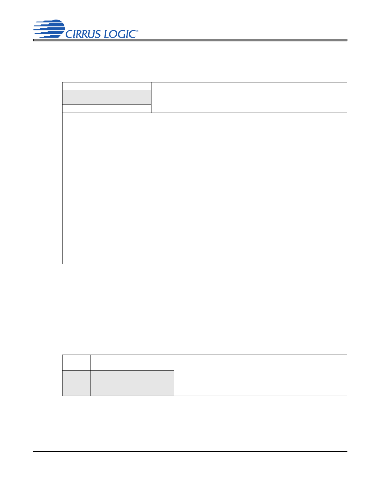
6.17.4 PGA Soft-Ramp
Configures an incremental volume ramp from the current level to the new level at the specified rate. If PGA
Soft-Ramping is enabled (PGASFT = 1b), the effect of changes to the PGA analog volume controls (listed
below) are applied progressively (see exceptions below); if disabled, changes are applied all at once.
PGASFT Volume Changes Affected Analog Volume Control
0 Abruptly take effect with-
out a soft-ramp
1 Occur with a soft-ramp
If (ALC is disabled)
// [PGA Volume setting is changed via PGAxVOL]
If (ANLGZC = 0b)
Else // [ANLGZC = 1b]
Else // (ALC is enabled)
If ((ALC attack soft-ramping is disabled) and (Considering attack ramp-rate))
Ramp Rate:
Else // [ALC attack soft-ramping is enabled] or [Considering release ramp-rate]]
Notes:
- ALC_Rate_Setting is either ALCARATE or ALCRRATE
- ALC is disabled via ALCx
- ALC attack soft-ramping can be disabled via ALCxSRDIS
PGAxVOL[5:0] (“PGAx Volume” on page 98)
0.5 dB every 32 Fs cycles
0.5 dB per ANLGZC event
If (ANLGZC = 0b)
Abrupt volume change
Else // (ANLGZC = 1b)
Abrupt volume change at next zero cross event
If (ANLGZC = 0b)
If (ALC_Rate_Setting < 2))
0.5 dB every 32 Fs cycles
Else // (ALC_Rate_Setting > 1)
0.5 x Fs / (16 * ALC_Rate_Setting + 1)
Else // [(ANLGZC = 1b)
0.5 x f
/ (16 * ALC_Rate_Setting + 1); f
step
CS42L73
is the freq. of zero cross events (including time-outs)
step
Notes:
• Refer to section “Analog Zero Cross” on page 95 for a description of the ANLGZC control.
• This register bit also affects the ALC volume attack and release rates (soft-ramped as a
function of Fs or abrupt). ALC attack soft-ramping can be disabled, regardless of this register control bit, via control “ALCx Soft-Ramp Disable” on page 116.
6.17.5 Analog Zero Cross
Configures when the signal-level changes occur for the analog volume controls. If Analog Zero Cross is
enabled (ANLGZC = 1b), the effect of changes to the affected analog volume controls (listed below) are
delayed to occur quietly at zero crossings; if disabled, changes will not be aligned to zero crosses.
ANLGZC Volume Changes Affected Analog Volume Controls
0 Do not occur on a zero crossing PGAxVOL[5:0] (“PGAx Volume” on page 98)
1 Occur on a zero crossing
Notes:
• If the signal does not encounter a zero crossing, the requested volume change will occur
after a timeout period of 1024 sample periods (approximately 21.3 ms at 48 kHz sample
rate).
• The size of the “Volume Change” per zero cross depends on whether soft-ramping is used
(refer to sections “PGA Soft-Ramp” on page 95 and “Analog Output Soft Ramp” on
HPxAMUTE (“Headphone x Analog Mute” on page 103)
HPxAVOL[6:0] (“Headphone x Analog Volume Control” on page 103)
LOxAMUTE (“Line Output x Analog Mute” on page 104)
LOxAVOL[6:0] (“Line Output x Analog Volume Control” on page 104)
DS882F1 95
Page 96

page 96). If soft-ramping is disabled, a single volume change will occur according to the
volume control change. If soft ramping is enabled, the volume change is the soft-ramp step
size. With zero cross and soft-ramping enabled, with each zero cross, the volume will step
until it eventually matches the volume control.
6.17.6 Digital Soft-Ramp
Configures an incremental volume ramp from the present level to the new level, at the specified rate. If
Digital Soft-Ramping is enabled (DIGSFT = 1b), the effect of changes to the affected digital volume controls (listed below) is applied progressively over time (see exceptions noted below); if disabled, changes
are applied abruptly, all at once.
DIGSFT Volume Changes Affected Digital Volume Controls
0 Abruptly take effect with-
out a soft-ramp
1 Occur with a soft-ramp
Soft-Ramp
Rate:
1/8 dB every Fs cycle
CS42L73
IPxMUTE (“Input Path x Digital Mute” on page 97)
IPxDVOL[7:0] (“Input Path x Digital Volume Control” on page 99)
HLxDMUTE (“Headphone/Line Output (HL) x Digital Mute” on page 101)
HLxDVOL[7:0] (“Headphone/Line Output (HL) x Digital Volume Control” on page 101)
ESLDMUTE (“Ear Speaker/Speakerphone Line Output Digital Mute” on page 100)
ESLDVOL[7:0] (“Ear Speaker/Speakerphone Line Output (ESL) [B] Digital Volume Con-
trol” on page 102)
SPKDMUTE (“Ear Speaker/Speakerphone Line Output Digital Mute” on page 100)
SPKDVOL[7:0] (“Speakerphone Out [A] Digital Volume Control” on page 102)
Notes:
• This register bit also sets the noise gate mute/unmute volume ramp rate.
• This register bit does not affect the digital mixer’s soft ramping. Register “Mixer Soft-Ramp
Enable” on page 117 configures the digital mixer’s soft ramping.
• This register bit also affects the ALC and Limiter digital volume attack and release rates
(soft-ramped at programmed rates or abrupt). The ALC and Limiter Attack soft-ramping
can be disabled, regardless of this register control bit, via the override controls “ALCx
Soft-Ramp Disable” on page 116 and “Limiter Soft-Ramp Disable” on page 100.
6.17.7 Analog Output Soft Ramp
Configures an incremental volume ramp from the present level to the new level, at the specified rate. If
Analog Output Soft-Ramping is enabled (ANLGOSFT = 1b), the effect of changes to the affected analog
volume controls (listed below) is applied progressively over time; if disabled, changes will be applied
abruptly, all at once.
ANLGOSFT Volume Changes Affected Analog Output Volume Controls
0 Abruptly take effect with-
1 Occur with a soft ramp
Ramp Rate:
out a soft-ramp
ANLGZC = 0b:
1.0 dB (-50 dB to +12 dB) or 2 dB (-76 dB to -50 dB) every 32 Fs cycles
ANLGZC = 1b:
1.0 dB per ANLGZC event
HPxAMUTE (“Headphone x Analog Mute” on page 103)
HPxAVOL[6:0] (“Headphone x Analog Volume Control” on page 103)
LOxAMUTE (“Line Output x Analog Mute” on page 104)
LOxAVOL[6:0] (“Line Output x Analog Volume Control” on page 104)
Notes:
• Refer to section “Analog Zero Cross” on page 95 for a description of the ANLGZC control.
96 DS882F1
Page 97

CS42L73
6.18 ADC/Input Path Control (Address 14h)
76543210
PGABMUX BOOSTB INV_ADCB IPBMUTE PGAAMUX BOOSTA INV_ADCA IPAMUTE
6.18.1 PGA x Input Select
Selects the specified analog input signal into channel x’s PGA.
PGAxMUX Selected Input to PGAA/PGAB
0 LINEINA/LINEINB
1MIC1/MIC2
Note: For pseudodifferential inputs, the CODEC automatically chooses the respective pseudoground
(LINEIN_REF or MIC1_REF, LINEIN_REF or MIC2_REF) for each input selection.
6.18.2 Boost x
Configures a +20 dB digital boost on channel x.
BOOSTx +20 dB Digital Boost
0 No boost applied
1 +20 dB boost applied
6.18.3 Invert ADCx Signal Polarity
Configures the polarity of the ADC channel x signal.
INV_ADCx ADCx Signal Polarity
0 Not Inverted
1 Inverted
6.18.4 Input Path x Digital Mute
Configures a digital mute on the volume control for Input Path channel x, overriding the Input Path digital
volume setting (IPxDVOL) and the associated ALC volume control.
IPxMUTE Input Path Mute
0 Not muted
1 Muted
DS882F1 97
Page 98
CS42L73
6.19 Mic PreAmp and PGA Volume Control: Channel A (Mic 1, Address 15h) and Channel B (Mic 2, Address 16h)
76 5 4 3 2 1 0
Reserved MIC_PREAMPx PGAxVOL5 PGAxVOL4 PGAxVOL3 PGAxVOL2 PGAxVOL1 PGAxVOL0
6.19.1 Mic PREAMP x Volume
Sets the gain of the mic preamp on channel x.
MIC_PREAMPx Volume
0 +10 dB
1 +20 dB
6.19.2 PGAx Volume
Normally, this control sets the attenuation/gain of the PGA on channel x. When the ALC is engaged, it
sets the maximum volume.
PGAxVOL[5:0] Volume
01 1111 12 dB
... ...
01 1000 12 dB
... ...
00 0001 +0.5 dB
00 0000 0 dB
11 1111 -0.5 dB
... ...
11 1010 -3.0 dB (Target setting for 600 mVrms analog input amplitude)
... ...
11 0100 -6.0 dB
... ...
10 0000 -6.0 dB
Step Size: 0.5 dB
Note: The step size may deviate slightly from 0.5 dB. Refer to Figures 42-47 on page 126.
98 DS882F1
Page 99

CS42L73
6.20 Input Path x Digital Volume Control: Channel A (Address 17h) and B (Address 18h)
76543210
IPxDVOL7 IPxDVOL6 IPxDVOL5 IPxDVOL4 IPxDVOL3 IPxDVOL2 IPxDVOL1 IPxDVOL0
6.20.1 Input Path x Digital Volume Control
Normally, this control sets the volume of the Input Path signal on channel x. When the ALC is engaged,
it sets the maximum volume. Input Path digital mutes (IPxMUTE) override this register control.
IPxDVOL[7:0] Volume
0111 1111 +12 dB
... ...
0000 1100 +12 dB
... ...
0000 0000 0 dB
1111 1111 -1 . 0 dB
1111 111 0 -2 . 0 dB
... ...
1010 0000 -96.0 dB
... ...
1000 0000 -96.0 dB
Step Size: 1.0 dB
DS882F1 99
Page 100

CS42L73
6.21 Playback Digital Control (Address 19h)
76543210
SES_
PLYBCKB=A
6.21.1 Speakerphone [A], Ear Speaker/Speakerphone Line Output [B] (SES)
6.21.2 Headphone/Line Output (HL) Playback Channels B=A
HL_PLYBCKB=A LIMSRDIS Reserved ESLDMUTE SPKDMUTE HLBDMUTE HLADMUTE
Playback Channels B=A
Configures independent or ganged volume control of the stereo playback channels. If ganging is enabled,
channel B’s volume will be equal to channel A’s, regardless of channel B’s programming (see affected
volume controls listed below).
SES_
PLYBCKB=A
0 Disabled;
1 Enabled;
Configures independent or ganged volume control of the stereo playback channels. If ganging is enabled,
channel B’s volume will be equal to channel A’s, regardless of channel B’s programming (see affected
volume controls listed below).
HL_
PLYBCKB=A
0 Disabled;
1 Enabled;
Single Volume Control (Ganging) Affected Volume Controls
Independent channel volume control.
Ganged channel volume control.
Channel A’s volume control controls
both A and B channels’ volume.
Single Volume Control (Ganging) Affected Volume Controls
Independent channel volume control.
Ganged channel volume control.
Channel A’s volume control controls
both A and B channels’ volume.
ESLDMUTE (“Ear Speaker/Speakerphone Line Output Digital Mute” on
page 100)
ESLDVOL[7:0] (“Ear Speaker/Speakerphone Line Output (ESL) [B] Digital
Volume Control” on page 102)
HLBDMUTE (“Headphone/Line Output (HL) x Digital Mute” on page 101)
HLBDVOL[7:0] (“Headphone/Line Output (HL) x Digital Volume Control” on
page 101)
HPBAMUTE and HPBAVOL[6:0] (“Headphone Analog Volume Control:
Channel A (Address 1Eh) and B (Address 1Fh)” on page 103)
LOBAMUTE and LOBAVOL[6:0] (“Line Output Analog Volume Control:
Channel A (Address 20h) and B (Address 21h)” on page 104)
6.21.3 Limiter Soft-Ramp Disable
Configures an override of the Limiter Attack soft-ramp setting.
LIMSRDIS Limiter Soft-Ramp Disable
0 OFF; Limiter Attack Rate is dictated by the DIGSFT (“Digital Soft-Ramp” on page 96) setting
1 ON; Limiter Attack volume changes take effect in one step, regardless of the DIGSFT setting
6.21.4 Ear Speaker/Speakerphone Line Output Digital Mute
Configures a digital mute on the volume control for ear speaker, overriding the Ear Speaker/Speakerphone Line Output digital volume setting (ESLDVOL) and the associated Limiter volume control.
ESLDMUTE Ear Speaker/Speakerphone Line Output Digital Mute
0 Not muted
1 Muted
100 DS882F1
 Loading...