

Page 1
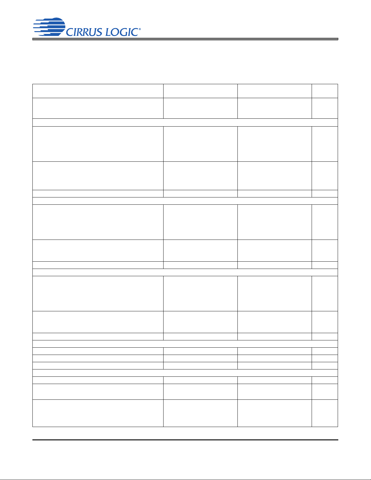
HPF
+1.62 V to +3.63 V
Interface Supply
Control Port
Serial Audio Port
Level Shifter
Multi-bit
ADC
Beep
Multi-bit
ADC
ALC
ALC
Multi-bit
DAC
Mono mix,
Limiter, Bass,
Treble Adjust
Attenuator,
Boost, Mix
Left Line Output
Right Line Output
Pseudo Diff. Input
I²S or Left Justified
Serial Audio Input/
Output
I²C or SPI
Control
Digital Supply (VLDO)
+1.62 V to +2.75 V
Analog Supply (VA)
+1.62 V to +2.75 V
LDO Regulator
InvertingStep-Down
+VHP
-VHP
Charge Pump Supply (VCP)
+1.62 V to +2.75 V
Ground-Centered
Amplifiers
Left Headphone Output
-
+
Right Headphone Output
+
-
+
-
-
+
Programmable Mic Bias
Mic Bias Output
Left Input 1
Pseudo Diff. Input /
Left Input 3
Right Input 1
Left Input 2
Pseudo Diff. Input /
Right Input 3
Right Input 2
0, +10, or
+20 dB
-6 to +12 dB
0.5 dB Steps
Pseudo Diff. Input
CS42L56
Ultralow Power, Stereo Codec with Class H Headphone Amp
DIGITAL to ANALOG FEATURES
5 mW Stereo Playback Power Consumption
99 dB Dynamic Range (A-wtd)
-86 dB THD+N
Digital Signal Processing Engine
– Bass & Treble Tone Control, De-emphasis
– Master Volume Control (+12 to -102 dB in
0.5 dB steps)
– Soft-ramp & Zero-cross Transitions
– Programmable Peak-detect and Limiter
– Beep Generator with Full Tone Control
Stereo Headphone and Line Amplifiers
Step-down/Inverting Charge Pump
Class H Amplifier - Automatic Supply Adj.
– High Efficiency
– Low EMI
Pseudo-differential Ground-centered Outputs
High HP Power Output at -75 dB THD+N
– 2 x 20 mW Into 16 @ 1.8 V
1V
Analog Vol. Ctl. (+12 to -60 dB in 1 dB steps)
Analog In to Analog Out Passthrough
Pop and Click Suppression
Line Output @ 1.8 V
RMS
ANALOG to DIGITAL FEATURES
3.5 mW Stereo Record Power Consumption
95 dB Dynamic Range (A-wtd)
-87 dB THD+N
Configurable Analog Inputs
– Two Pseudo-differential Stereo Inputs or
– One Pseudo-differential Stereo Inputs +
One Standard Stereo Input + One Standard
Mono Input or
– Three Standard Stereo Inputs
– Pseudo-differential Inputs Reduce
Common Mode Signal Noise
– 3:1 Stereo Input MUX for ADC or
Passthrough
Analog Programmable Gain Amplifier (PGA)
– +12 to -6 dB in 0.5 dB steps
– +10 dB or +20 dB Additional Gain for
Microphone Inputs
Programmable, Low-noise MIC Bias Output
Programmable Automatic Level Control (ALC)
– Noise Gate for Noise Suppression
– Programmable Threshold &
Attack/Release Rates
Independent ADC Channel Control
High-pass Filter Disable for DC Measurements
http://www.cirrus.com
Copyright Cirrus Logic, Inc. 2014
(All Rights Reserved)
FEB '14
DS851F2
Page 2

CS42L56
SYSTEM FEATURES
Audio (11.2896 MHz or 12.288 MHz) or USB
(12 MHz) Master Clock Input
Low-power Operation
– Stereo Anlg. Passthrough: 3.3 mW @1.8 V
– Stereo Rec. and Playback: 8.3 mW @1.8 V
Headphone Detect Input
High Performance 24-bit Converters
– Multi-bit Delta–Sigma Architecture
Integrated High Efficient Power Management
Reduces Power Consumption
– Step-down Charge Pump Improves
Efficiency
– Inverting Charge Pump Accommodates
Low System Voltage by Providing Negative
Rail for HP/Line Amp
– LDO Reg. Provides Low Digital Supply
Voltage
Digital Power Reduction
– Very Low ADC/DAC Oversampling Rate
– Bursted Serial Clock Providing up to 24 Bits
per Sample
Power Down Management
– ADC, DAC, CODEC, PGA, DSP
Analog & Digital Routing/Mixes
– Line/Headphone Out = Analog In (ADC
Bypassed)
– Line/Headphone Out = ADC Out
– Internal Digital Loopback
– Mono Mixes
I²C or SPI™ Control Port
I²S or Left-justified Digital Interface Format
Flexible Clocking Options
– Master or Slave Operation
– Wide Range of Sample Rates Supported
APPLICATIONS
HDD and Flash-based Portable Audio Players
PDAs
Personal Media Players
Portable Game Consoles
Digital Voice Recorders
MD Players/Recorders
Digital Camcorders
Digital Cameras
GENERAL DESCRIPTION
The CS42L56 is a highly integrated, 24-bit, ultra-lowpower stereo CODEC based on multi-bit delta-sigma
modulation. Both the ADC and DAC offer many features
suitable for low power portable system applications.
The analog input path allows independent channel
control of a variety of features. The Programmable Gain
Amplifier (PGA) provides analog gain with zero cross
transitions. The ADC path includes a digital volume attenuator with soft ramp transitions and a programmable
ALC and noise gate monitor the input signals and adjust
the volume appropriately. An analog passthrough also
exists, accommodating a lower noise, lower power analog in to analog out path to the headphone and line
amplifiers, bypassing the ADC and DAC.
The DAC output path includes a fixed-function digital
signal processing engine. Tone control provides bass
and treble adjustment at four selectable corner frequencies. The digital mixer provides independent volume
control for both the ADC output and PCM input signal
paths, as well as a master volume control. Digital volume controls may be configured to change on soft ramp
transitions while the analog controls can be configured
to occur on every zero crossing. The DAC path also includes de-emphasis, limiting functions and a beep
generator delivering tones selectable across a range of
two full octaves.
The Class H stereo headphone amplifier combines the
efficiency of an integrated step-down and inverting
charge pump with the linearity and low EMI of a Class
AB amplifier. A step-down/inverting charge pump operates in two modes: ±VCP mode or ±VCP/2) mode.
Based on the amplifier’s output signal, internal logic automatically adjusts the output of the charge pump,
+VHPFILT and –VHPFILT, to optimize efficiency. With
these features, the amplifier delivers a ground-centered
output with a large signal swing even at low voltages
and eliminates the need for external DC-blocking
capacitors.
These features make the CS42L56 the ideal solution for
portable applications which require extremely low power consumption in a minimal amount of space.
The CS42L56 is available in a 40-pin QFN package for
the Commercial (-40 to +85° C) grade. The CDB42L56
Customer Demonstration board is also available for device evaluation and implementation suggestions.
Please see “Ordering Information” on page 93 for complete details.
Smart Phones
2 DS851F2
Page 3

TABLE OF CONTENTS
1. PIN DESCRIPTIONS .............................................................................................................................. 8
1.1 I/O Pin Characteristics .................................................................................................................... 10
2. TYPICAL CONNECTION DIAGRAMS .................................................................................................11
3. CHARACTERISTIC AND SPECIFICATION TABLES ......................................................................... 14
RECOMMENDED OPERATING CONDITIONS ................................................................................... 14
ABSOLUTE MAXIMUM RATINGS .......................................................................................................14
ANALOG INPUT CHARACTERISTICS ................................................................................................ 14
ADC DIGITAL FILTER CHARACTERISTICS ....................................................................................... 17
HP OUTPUT CHARACTERISTICS ......................................................................................................18
LINE OUTPUT CHARACTERISTICS ................................................................................................... 19
ANALOG PASSTHROUGH CHARACTERISTICS ............................................................................... 21
COMBINED DAC INTERPOLATION & ON-CHIP ANALOG FILTER RESPONSE ...............................21
SWITCHING SPECIFICATIONS - SERIAL PORT ............................................................................... 22
SWITCHING SPECIFICATIONS - I²C CONTROL PORT ..................................................................... 23
SWITCHING CHARACTERISTICS - SPI CONTROL PORT ................................................................ 24
ANALOG OUTPUT ATTENUATION CHARACTERISTICS .................................................................. 25
DC CHARACTERISTICS ...................................................................................................................... 26
DIGITAL INTERFACE SPECIFICATIONS & CHARACTERISTICS ..................................................... 27
POWER CONSUMPTION - ALL SUPPLIES = 1.8 V ............................................................................ 28
POWER CONSUMPTION - ALL SUPPLIES = 2.5 V ........................................................................... 29
4. APPLICATIONS ................................................................................................................................... 30
4.1 Overview ......................................................................................................................................... 30
4.1.1 Basic Architecture ................................................................................................................. 30
4.1.2 Line Inputs ............................................................................................................................. 30
4.1.3 Line and Headphone Outputs (Class H, Ground-Centered Amplifiers) ................................. 30
4.1.4 Fixed-function DSP Engine ................................................................................................... 30
4.1.5 Beep Generator ..................................................................................................................... 30
4.1.6 Power Management .............................................................................................................. 30
4.2 Analog Inputs .................................................................................................................................. 31
4.2.1 Pseudo-differential Inputs ...................................................................................................... 32
4.2.2 Large-scale Inputs ................................................................................................................. 32
4.2.3 Microphone Inputs ................................................................................................................. 34
4.2.3.1 External Passive Components ................................................................................... 34
4.2.4 Optional VCM Buffer ............................................................................................................. 34
4.2.5 Automatic Level Control (ALC) .............................................................................................. 34
4.2.5.1 Attack/Release Time Calculations: ............................................................................ 36
4.3 Analog In to Analog Out Passthrough ............................................................................................ 36
4.4 Analog Outputs .............................................................................................................................. 37
4.5 Class H Amplifier ............................................................................................................................ 38
4.5.1 Power Control Options .......................................................................................................... 39
4.5.1.1 Standard Class AB Mode (setting 01 and 10) ........................................................... 39
4.5.1.2 Adapt to Volume Mode (setting 00) ........................................................................... 39
4.5.1.3 Adapt to Output Mode (setting 11) ............................................................................. 42
4.5.2 Power Supply Transitions ...................................................................................................... 42
4.5.3 Efficiency ............................................................................................................................... 43
4.6 Beep Generator .............................................................................................................................. 44
4.7 Limiter ....................................................................................................................
4.8 Serial Port Clocking ........................................................................................................................ 46
4.9 Digital Interface Format .................................................................................................................. 49
4.10 Initialization ................................................................................................................................... 49
4.11 Recommended DAC to HP or Line Power Sequence .................................................................. 49
4.11.1 Power-Up Sequence ........................................................................................................... 49
CS42L56
...................... 45
...
DS851F2 3
Page 4

CS42L56
4.11.2 Power-Down Sequence ....................................................................................................... 50
4.12 Recommended PGA to HP or Line Power Sequence (Analog Passthrough) .............................. 51
4.12.1 Power-Up Sequence ........................................................................................................... 51
4.12.2 Power-Down Sequence ....................................................................................................... 52
4.13 Control Port Operation .................................................................................................................. 53
4.13.1 SPI Control .......................................................................................................................... 53
4.13.2 I²C Control ........................................................................................................................... 53
4.13.3 Memory Address Pointer (MAP) .......................................................................................... 54
4.13.3.1 Map Increment (INCR) ............................................................................................. 54
5. REGISTER QUICK REFERENCE ........................................................................................................ 55
6. REGISTER DESCRIPTION .................................................................................................................. 57
6.1 Device I.D. Register (Address 01h) (Read Only) ............................................................................ 57
6.1.1 Device I.D. (Read Only) ........................................................................................................ 57
6.2 Device Revision Register (Address 02h) (Read Only) ................................................................... 57
6.2.1 Alpha Revision (Read Only) .................................................................................................. 57
6.2.2 Numeric Revision (Read Only) .............................................................................................. 57
6.3 Power Control 1 (Address 03h) ...................................................................................................... 57
6.3.1 Power Down VCM Bias Buffer .............................................................................................. 57
6.3.2 Power Down MIC Bias .......................................................................................................... 58
6.3.3 Power Down ADC Charge Pump .......................................................................................... 58
6.3.4 Power Down ADC x ............................................................................................................... 58
6.3.5 Power Down .......................................................................................................................... 58
6.4 Power Control 2 (Address 04h) ...................................................................................................... 58
6.4.1 Headphone Power Control .................................................................................................... 58
6.4.2 Line Power Control ................................................................................................................ 59
6.5 Clocking Control 1 (Address 05h) ................................................................................................... 59
6.5.1 Master/Slave Mode ............................................................................................................... 59
6.5.2 SCLK Polarity ........................................................................................................................ 59
6.5.3 SCLK Equals MCLK .............................................................................................................. 59
6.5.4 MCLK Pre-Divide ................................................................................................................... 59
6.5.5 MCLK Divide ......................................................................................................................... 60
6.5.6 MCLK Disable ....................................................................................................................... 60
6.6 Clocking Control 2 (Address 06h) ................................................................................................... 60
6.6.1 Clock Ratio Auto-Detect ........................................................................................................ 60
6.6.2 Clock Ratio ............................................................................................................................ 61
6.7 Serial Format (Address 07h) .......................................................................................................... 61
6.7.1 CODEC Digital Interface Format ...........................................................................................61
6.8 Class H Control (Address 08h) ....................................................................................................... 62
6.8.1 Adaptive Power Adjustment .................................................................................................. 62
6.8.2 Charge Pump Frequency ...................................................................................................... 62
6.9 Misc. Control (Address 09h) ........................................................................................................... 62
6.9.1 Digital MUX ........................................................................................................................... 62
6.9.2 Analog Soft Ramp ................................................................................................................. 63
6.9.3 Analog Zero Cross ................................................................................................................ 63
6.9.4 Digital Soft Ramp .................................................................................................................. 63
6.9.5 Freeze Registers ................................................................................................................... 63
6.10 Status (Address 0Ah) (Read Only) ............................................................................................... 64
................................................................................ 64
6.10.1 HPDETECT Pin Status (Read Only)
6.10.2 Serial Port Clock Error (Read Only) .................................................................................... 64
6.10.3 DSP Engine Overflow (Read Only) ..................................................................................... 64
6.10.4 MIXx Overflow (Read Only) ................................................................................................. 64
6.10.5 ADCx Overflow (Read Only) ...............................................................................................64
6.11 Playback Control (Address 0Bh) .................................................................................................. 65
6.11.1 Power Down DSP ................................................................................................................ 65
...
4 DS851F2
Page 5

CS42L56
6.11.2 HP/Line De-Emphasis ......................................................................................................... 65
6.11.3 Playback Channels B=A ...................................................................................................... 65
6.11.4 Invert PCM Signal Polarity .................................................................................................. 65
6.12 DSP Mute Controls (Address 0Ch) ............................................................................................... 66
6.12.1 ADC Mixer Channel x Mute ................................................................................................. 66
6.12.2 PCM Mixer Channel x Mute ................................................................................................66
6.12.3 Master Playback Mute ......................................................................................................... 66
6.13 ADCx Mixer Volume: ADCA (Address 0Dh) & ADCB (Address 0Eh) ........................................... 66
6.13.1 ADC Mixer Channel x Volume ............................................................................................. 66
6.14 PCMx Mixer Volume: PCMA (Address 0Fh) & PCMB (Address 10h) .......................................... 67
6.14.1 PCM Mixer Channel x Volume ............................................................................................ 67
6.15 Analog Input Advisory Volume (Address 11h) .............................................................................. 68
6.15.1 Analog Input Advisory Volume ............................................................................................68
6.16 Digital Input Advisory Volume (Address 12h) ...............................................................................68
6.16.1 Digital Input Advisory Volume ............................................................................................. 68
6.17 Master Volume Control:
MSTA (Address 13h) & MSTB (Address 14h) ...................................................................................... 69
6.17.1 Master Volume Control ........................................................................................................ 69
6.18 Beep Frequency & On Time (Address 15h) ................................................................................. 69
6.18.1 Beep Frequency .................................................................................................................. 69
6.18.2 Beep On Time ..................................................................................................................... 70
6.19 Beep Volume & Off Time (Address 16h) ......................................................................................70
6.19.1 Beep Off Time ..................................................................................................................... 70
6.19.2 Beep Volume ....................................................................................................................... 71
6.20 Beep & Tone Configuration (Address 17h) ...................................................................................71
6.20.1 Beep Configuration .............................................................................................................. 71
6.20.2 Treble Corner Frequency .................................................................................................... 71
6.20.3 Bass Corner Frequency ...................................................................................................... 72
6.20.4 Tone Control Enable ........................................................................................................... 72
6.21 Tone Control (Address 18h) ......................................................................................................... 72
6.21.1 Treble Gain .......................................................................................................................... 72
6.21.2 Bass Gain ............................................................................................................................ 72
6.22 ADC & PCM Channel Mixer (Address 19h) .................................................................................. 73
6.22.1 PCM Mix Channel Swap ..................................................................................................... 73
6.22.2 ADC Mix Channel Swap ...................................................................................................... 73
6.23 AIN Reference Configuration, ADC MUX (Address 1Ah) ............................................................. 73
6.23.1 Analog Input 2 x Reference Configuration .......................................................................... 73
6.23.2 Analog Input 1 x Reference Configuration .......................................................................... 73
6.23.3 ADC x Input Select .............................................................................................................. 74
6.24 HPF Control (Address 1Bh) .......................................................................................................... 74
6.24.1 ADCx High-Pass Filter ........................................................................................................ 74
6.24.2 ADCx High-Pass Filter Freeze ............................................................................................74
6.24.3 HPF x Corner Frequency .................................................................................................... 74
6.25 Misc. ADC Control (Address 1Ch) ................................................................................................ 75
6.25.1 ADC Channel B=A .............................................................................................................. 75
6.25.2 PGA Channel B=A .............................................................................................................. 75
6.25.3 Digital Sum .......................................................................................................................... 75
6.25.4 Invert ADC Signal Polarity ................................................................................................... 75
6.25.5 ADC Mute ............................................................................................................................ 75
6.26 Gain & Bias Control (Address 1Dh) ........................................................................................
PGA
6.26.1
6.26.2 Boostx ................................................................................................................................. 76
6.26.3 Microphone Bias Output Level ............................................................................................76
6.27 PGA x MUX, Volume: PGA A (Address 1Eh) & PGA B (Address 1Fh) ........................................ 76
x Preamplifier Gain ..................................................................................................... 76
...... 76
DS851F2 5
Page 6

CS42L56
6.27.1 PGA x Input Select .............................................................................................................. 76
6.27.2 PGAx Volume ...................................................................................................................... 77
6.28 ADCx Attenuator Control: ADCAATT (Address 20h) & ADCBATT (Address 21h) ....................... 77
6.28.1 ADCx Volume ...................................................................................................................... 77
6.29 ALC Enable & Attack Rate (Address 22h) ....................................................................................78
6.29.1 ALCx .................................................................................................................................... 78
6.29.2 ALC Attack Rate .................................................................................................................. 78
6.30 ALC Release Rate (Address 23h) ................................................................................................ 78
6.30.1 ALC Limit All Channels ........................................................................................................ 78
6.30.2 ALC Release Rate ............................................................................................................... 79
6.31 ALC Threshold (Address 24h) ...................................................................................................... 79
6.31.1 ALC Maximum Threshold .................................................................................................... 79
6.31.2 ALC Minimum Threshold ..................................................................................................... 80
6.32 Noise Gate Control (Address 25h) ............................................................................................... 80
6.32.1 Noise Gate All Channels ..................................................................................................... 80
6.32.2 Noise Gate Enable .............................................................................................................. 80
6.32.3 Noise Gate Threshold and Boost ........................................................................................ 81
6.32.4 Noise Gate Delay Timing .................................................................................................... 81
6.33 ALC and Limiter Soft Ramp, Zero Cross Disables (Address 26h) ................................................ 81
6.33.1 ALCx Soft Ramp Disable ..................................................................................................... 81
6.33.2 ALCx Zero Cross Disable .................................................................................................... 81
6.33.3 Limiter Soft Ramp Disable ................................................................................................... 81
6.34 Automute, Line & HP MUX (Address 27h) ................................................................................... 82
6.34.1 Auto Mute ............................................................................................................................ 82
6.34.2 Line Input Select .................................................................................................................. 82
6.34.3 Headphone Input Select ...................................................................................................... 82
6.35 Headphone Volume Control: HPA (Address 28h) & HPB (Address 29h) ..................................... 82
6.35.1 Headphone Channel x Mute ................................................................................................82
6.35.2 Headphone Volume Control ................................................................................................83
6.36 Line Volume Control: LINEA (Address 2Ah) & LINEB (Address 2Bh) .......................................... 83
6.36.1 Line Channel x Mute ........................................................................................................... 83
6.36.2 Line Volume Control ............................................................................................................ 83
6.37 Limiter Min/Max Thresholds (Address 2Ch) ................................................................................. 84
6.37.1 Limiter Maximum Threshold ................................................................................................ 84
6.37.2 Limiter Cushion Threshold .................................................................................................. 84
6.38 Limiter Control, Release Rate (Address 2Dh) .............................................................................. 85
6.38.1 Peak Detect and Limiter ...................................................................................................... 85
6.38.2 Peak Signal Limit All Channels ........................................................................................... 85
6.38.3 Limiter Release Rate ...................................................................................................
39 Limit
6.
7. PCB LAYOUT CONSIDERATIONS ..................................................................................................... 87
7.1 Power Supply ................................................................................................................................. 87
7.2 Grounding ....................................................................................................................................... 87
7.3 QFN Thermal Pad .......................................................................................................................... 87
8. ANALOG VOLUME NON-LINEARITY (DNL & INL) ............................................................................ 88
9. ADC & DAC DIGITAL FILTERS .......................................................................................................... 89
10. PARAMETER DEFINITIONS .............................................................................................................. 90
11. PACKAGE DIMENSIONS .................................................................................................................. 91
THERMAL CHARACTERISTICS .......................................................................................................... 91
12. ORDERING INFORMATION .............................................................................................................. 92
13. REFERENCES .................................................................................................................................... 92
14. REVISION HISTORY .......................................................................................................................... 92
er Attack Rate (Address 2Eh) ............................................................................................... 86
6.39.1 Limiter Attack Rate .............................................................................................................. 86
........ 85
6 DS851F2
Page 7

LIST OF FIGURES
Figure 1.Typical Connection Diagram - Four Pseudo-Differential Analog Inputs ...................................... 11
Figure 2.Typical Connection Diagram - Two Pseudo-Differential / Three Single-Ended Analog Inputs ... 12
Figure 3.Typical Connection Diagram - Six Single-Ended Analog Inputs ................................................. 13
Figure 4.CMRR Test Configuration ........................................................................................................... 16
Figure 5.AINxREF Input Voltage Test Configuration ................................................................................ 16
Figure 6.HP Output Test Configuration ..................................................................................................... 20
Figure 7.Line Output Test Configuration ................................................................................................... 20
Figure 8.Serial Port Timing (Slave Mode) ................................................................................................. 22
Figure 9.Serial Port Timing (Master Mode) ............................................................................................... 22
Figure 10.I²C Control Port Timing ............................................................................................................. 23
Figure 11.Control Port Timing - SPI Format .............................................................................................. 24
Figure 12.Power Consumption Test Configuration ................................................................................... 27
Figure 13.Analog Input Signal Flow .......................................................................................................... 31
Figure 14.Stereo Pseudo-Differential Input ............................................................................................... 32
Figure 15.Analog Input Attenuation ........................................................................................................... 33
Figure 16.Example Analog Input Attenuation ............................................................................................ 33
Figure 17.MIC Input Mix w/Common Mode Rejection ............................................................................... 34
Figure 18.ALC Operation .......................................................................................................................... 35
Figure 19.DSP Engine Signal Flow ........................................................................................................... 37
Figure 20.Analog Output Stage ................................................................................................................. 38
Figure 21.Class H Volume-Adapt Paths ................................................................................................... 39
Figure 22.Volume Sum Effects ................................................................................................................. 40
Figure 23.Channel/Amp Effect .................................................................................................................. 40
Figure 24.HP/Line Channel Effects ........................................................................................................... 41
Figure 25.VHPFILT Transitions ................................................................................................................. 42
Figure 26.VHPFILT Hysteresis ................................................................................................................. 43
Figure 27.Class H Power to Load vs. Power from VCP Supply - 32 W .................................................... 43
Figure 28.Class H Power to Load vs. Power from VCP Supply - 16 W .................................................... 44
Figure 29.Beep Configuration Options ...................................................................................................... 45
Figure 30.Peak Detect & Limiter ............................................................................................................... 46
Figure 31.Serial Port Timing in Master Mode ............................................................................................ 48
Figure 32.I²S Format ................................................................................................................................. 49
Figure 33.Left-Justified Format ................................................................................................................. 49
Figure 34.Control Port Timing in SPI Mode .............................................................................................. 53
Figure 35.Control Port Timing, I²C Write ................................................................................................... 54
Figure 36.Control Port Timing, I²C Read ................................................................................................... 54
Figure 37.PGA Step Size vs. Volume Setting ........................................................................................... 88
Figure 38.PGA Output Volume vs. Volume Setting .................................................................................. 88
Figure 39.HP/Line Step Size vs. Volume Setting ...................................................................................... 88
Figure 40.HP/Line Output Volume vs. Volume Setting .............................................................................88
Figure 41.ADC Frequency Response ....................................................................................................... 89
Figure 42.ADC Stopband Rejection .......................................................................................................... 89
Figure 43.ADC Transition Band ................................................................................................................ 89
Figure 44.ADC Transition Band Detail ...................................................................................................... 89
Figure 45.DAC Frequency Response ....................................................................................................... 89
Figure 46.DAC Stopband .......................................................................................................................... 89
Figure 47.DAC Transition Band ....................................................................................................
Figure 48.DAC Transition Band (Detail) .................................................................................................... 89
CS42L56
......... 89
...
DS851F2 7
Page 8
1. PIN DESCRIPTIONS
12
11
13
14
15
16
17
18
19
20
29
30
28
27
26
25
24
23
22
21
39
40
38
37
36
35
34
33
32
31
2
1
3
4
5
6
7
8
9
10
GND/Thermal Pad
VDFILT
VL
SDOUT
MCLK
SDIN
SCLK
-VHPFILT
HPREF
HPOUTB
TSTN
LINEOUTB
VA
AGND
AFILTB
SDA/CDIN
SCL/CCLK
AD0/CS
+VHPFILT
RESET
FLYC
FLYN
FILT+
AIN2A
MICBIAS
AIN1REF/AIN3A
AFILTA
AIN1A
AIN1B
VQ
FLYP
LRCK
VLDO
VCP
HPOUTA
TSTN
LINEOUTA
LINEREF
AIN2B
HPDETECT
AIN2REF/AIN3B
Top-Down (Through-Package) View
40-Pin QFN Package
CS42L56
Pin Name # Pin Description
SDIN 1 Serial Audio Data Input (Input) - Input for two’s complement serial audio data.
LRCK 2
SDA/CDIN
SCL/CCLK
AD0/CS
VCP 6 Step-Down Charge Pump Power (Input) - Power supply for the step-down charge pump.
FLYP 7
+VHPFILT 8
FLYC 9
FLYN 10
8 DS851F2
Left Right Clock (Input/Output) - Determines which channel, Left or Right, is currently active on the
serial audio data lines.
Serial Control Data (Input/Output) - SDA is the bidirectional data pin for the I²C control interface.
3
CDIN is the input data pin for the SPI control interface.
Serial Control Port Clock (Input) - Serial clock for the I²C and SPI control interfaces.
4
Chip Address (I²C) / Chip Select (SPI) (Input) - For I²C operation, this pin must remain static high
5
or low. For SPI, CS
Charge Pump Cap Positive Node (Output) - Positive node for the step-down charge pump’s flying
capacitor.
Step-Down Charge Pump Filter Connection (Output) - Power supply from the step-down charge
pump that provides the positive rail for the headphone and line amplifiers
Charge Pump Cap Common Node (Output) - Common positive node for the step-down and invert-
ing charge pumps’ flying capacitors.
Charge Pump Cap Negative Node (Output) - Negative node for the inverting charge pump’s flying
capacitor.
is the chip-select pin.
Page 9
CS42L56
-VHPFILT 11
HPOUTA
HPOUTB
HPREF 13
TSTN
LINEOUTA
LINEOUTB
LINEREF 18 Pseudo Diff. Line Output Reference (Input) - Ground reference for the line amplifiers.
VA 20 Analog Power (Input) - Power supply for the internal analog section.
AGND 21 Analog Ground (Input) - Ground reference for the internal analog section.
FILT+ 22 Positive Voltage Reference (Output) - Positive reference voltage for the internal sampling circuits.
VQ 23 Quiescent Voltage (Output) - Filter connection for the internal quiescent voltage.
AFILTA
AFILTB
MICBIAS
AIN1A
AIN1B
AIN2A
AIN2B
AIN1REF/AIN3A
AIN2REF/AIN3B2831
HPDETECT 33
RESET
VLDO 35 Low Dropout Regulator (LDO) Power (Input) - Power supply for the LDO regulator.
VDFILT 36
VL 37
SDOUT 38 Serial Audio Data Output (Output) - Output for two’s complement serial audio data.
MCLK 39 Master Clock (Input) - Clock source for the delta-sigma modulators.
SCLK 40 Serial Clock (Input/Output) - Serial clock for the serial audio interface.
GND/
Thermal Pad
Inverting Charge Pump Filter Connection (Output) - Power supply from the inverting charge
pump that provides the negative rail for the headphone and line amplifiers.
1214Headphone Audio Output (Output) - The full-scale output level is specified in “HP Output Charac-
teristics” on page 19.
Pseudo Diff. Headphone Output Reference (Input) - Ground reference for the headphone amplifi-
ers
Test Input (Input) - This pin is an input used for test purposes only and should be tied to ground for
15
normal operation.
16
1719Line Audio Output (Output) - The full-scale output level is specified in “Line Output Characteristics”
on page 20.
24
Antialias Filter Connection (Output) - Antialias filter connection for the ADC inputs.
25
Microphone Bias (Output) - Low noise bias supply for an external microphone. Electrical character-
26
istics are specified in the DC Electrical Characteristics table.
27
29
An
30
page 14.
32
Pseudo Differential Analog Input Reference/Analog Input 3 (Input) - Configurable as the ground
reference for the programmable gain amplifiers (PGA) or as additional analog inputs. The full-scale
level is specified in “Analog Input Characteristics” on page 14.
Headphone Detect (Input) - The HPDETECT circuit can be set to control the power down of the left
and/or right channel of the line and/or headphone outputs as described in “Headphone Power Con-
trol” on page 59 and “Line Power Control” on page 60 and/or cause an interrupt. This pin is
debounced such that the signal must remain stable in the new state for approximately 10 ms before
a change is passed on to the internal HPDETECT circuit.
34 Reset (Input) - The device enters a low power mode when this pin is driven low.
Low Dropout Regulator (LDO) Filter Connection (Output) - Power supply from the LDO regulator
that provides the low voltage power to the digital section.
Digital Interface Power (Input) - Determines the required signal level for the serial audio interface
and I²C control port.
- Ground reference for the internal charge pump and digital section; thermal relief pad.
Inputs 1 & 2 (Input) - The full-scale level is specified in “Analog Input Characteristics” on
alog
DS851F2 9
Page 10
1.1 I/O Pin Characteristics
Input and output levels and associated power supply voltage are shown in the table below. Logic levels
should not exceed the corresponding power supply voltage.
CS42L56
Power
Supply
VL
VA HPDETECT Input - - 1.8 V - 2.5 V, with Hysteresis
Pin Name I/O Internal
Connections
RESET
SCL Input - - 1.8 V - 3.3 V, with Hysteresis
SDA Input/Output - CMOS/Open Drain 1.8 V - 3.3 V, with Hysteresis
AD0 Input - - 1.8 V - 3.3 V, with Hysteresis
CCLK Input - - 1.8 V - 3.3 V, with Hysteresis
CDIN Input - - 1.8 V - 3.3 V, with Hysteresis
CS
MCLK Input - - 1.8 V - 3.3 V
LRCK Input/Output
SCLK Input/Output
SDOUT Output
SDIN Input - - 1.8 V - 3.3 V
Input - - 1.8 V - 3.3 V, with Hysteresis
Input - - 1.8 V - 3.3 V, with Hysteresis
Weak Pull-up
(~1 M
Weak Pull-up
(~1 M
Weak Pull-up
(~1 M
Driver Receiver
1.8 V - 3.3 V, CMOS 1.8 V - 3.3 V
1.8 V - 3.3 V, CMOS 1.8 V - 3.3 V
1.8 V - 3.3 V, CMOS -
10 DS851F2
Page 11
2. TYPICAL CONNECTION DIAGRAMS
Note 1
Note 2
2.2 µF
Note 1
Analog
Input 1
Analog
Input 2
1 µF
GND/Thermal Pad
VL
0.1 µF
+1.65 V to +3.63 V
RESET
R
p
LRCK
MCLK
SCLK
2.2 µF
+VHPF ILT
VDFILT
LINEREF
SDIN
SDOUT
1 µF
AIN2REF
AIN1A
1800 pF
1800 pF
100 k
100
AIN1B
*
*
Digital Audio
Processor
AIN2A
1800 pF
1800 pF
AIN2B
*
*
FLYC
FLYN
-VHPFI LT
2. 2 µF
1 µF
1 µF
1 µF
1 µF
100 k
100
100
100
100 k
100 k
2.2 µ F
**
**
VCP
AIN1REF
1 µF
LINEOUTA
LINEOUTB
0.1 µF
VA
+1.65 V to +2.75 V
0.1 µF
VLDO
2.2 µF
VQ
AGND
NPO /C0G dielect ric c apacit ors.
1000 pF
AFILT A
AFILT B
1000 pF
2.2 µF
*
*
HPOUTB
HPOUTA
Headphone Out
Left & Right
33
0.1 µ F
HPDETECT
33
0.1 µ F
47 k
HPREF
FILT+
+1.65 V to +2.75 V
FLYP
2.2 µ F
**
**
**
Note 1
Notes:
1. T he headphone amplif ier’s out put pow er and dist ortion are rat ed using t he nominal c apacit ance s hown. Larger capacit ance
reduces the ripple on the int ernal amplif iers’ s upplies and in turn redu ces the am plifier’s dist ortion at high outpu t pow er levels.
Smaller c apacit ance m ay not suff icie ntly re duce ripple t o achiev e the rat ed output power and dis tort ion. Since the act ual val ue
of ty pica l X7R/X5R c eramic capac itors deviat es f rom the nom inal va lue by a perc entage sp ecif ied in the m anufac turer’s data
sheet , capacit ors shoul d be select ed based on the minim um out put pow er and max imum dist ortion required.
2. T he headphone amplif ier’s out put pow er and dist ortion are rat ed using t he nominal c apacit ance s hown and us ing the def ault
charge pum p swi tchi ng frequenc y. The required capacit ance f ollows an invers e relations hip wit h the c harge pump’s sw itc hing
frequenc y. When increasing t he sw itc hing frequenc y, the capacit ance m ay dec rease; when lowering the swit ching f requency,
the c apacit ance m ust increas e. Since t he act ual value of ty pical X7R/ X5R c eramic capac itors deviat es f rom t he nom inal value
by a perc entage s pecif ied in t he manuf actu rer’s dat a sheet, capac itors should b e selec ted bas ed on the m inimum outp ut
power , max imum dis tort ion and max imum charge pum p sw itc hing frequenc y required.
3. Addit ional bulk c apacit ance m ay be added t o improv e PSRR at low f requenc ies.
4. T hese c apacit ors s erve as a charge res ervoir f or the int ernal sw itc hed capac itor AD C m odulators and should be plac ed as
clos e as pos sible t o the input s. They are only needed wh en the PGA (Program mable Gain Am plifier ) is bypass ed.
Note 4
Note 3
R
p
*
**
Low ESR, X7R/X5R dielec tric capac itors.
**
**
**
**
**
**
**
**
**
** **
**
**
**
562
562
3300 pF
R
ext
R
ext
LPF i s Opti onal
Line Level Out
Left & Right
3300 pF
*
*
SCL\CCLK
SDA\CD IN
AD0\CS
TSTN
TSTN
Figure 1. Typical Connection Diagram - Four Pseudo-Differential Analog Inputs
CS42L56
Notes:
1. The headphone amplifier’s output power and distortion are rated using the nominal capacitance shown. Larger capacitance reduces the ripple on the internal
amplifiers’ supplies and in turn reduces the amplifier’s distortion at high output power levels. Smaller capacitance may not sufficiently reduce ripple to achieve the
rated output power and distortion. Since the actual value of typical X7R/X5R ceramic capacitors deviates from the nominal value by a percentage specified in the
manufacturer’s data sheet, capacitors should be selected based on the minimum output power and maximum distortion required.
2. The headphone amplifier’s output power and distortion are rated using the nominal capacitance shown and using the default charge pump switching frequency.
The required capacitance follows an inverse relationship with the charge pump’s switching frequency. When increasing the switching frequency, the capacitance
may decrease; when lowering the switching frequency, the capacitance must increase. Since the actual value of typical X7R/X5R ceramic capacitors deviates
from the nominal value by a percentage specified in the manufacturer’s data sheet, capacitors should be selected based on the minimum output power, maximum
distortion and maximum charge pump switching frequency required.
3. Additional bulk capacitance may be added to improve PSRR at low frequencies.
4. These capacitors serve as a charge reservoir for the internal switched capacitor ADC modulators and should be placed as close as possible to the inputs. They
are only needed when the PGA (Programmable Gain Amplifier) is bypassed.
CS42L56
DS851F2 11
Page 12
CS42L56
2.2 µF
Note 1
**
Note 2
2.2 µF
Note 1
1 µF
GND/Thermal Pad
VL
0.1 µF
+1.65 V to +3.63 V
RESET
R
p
LRCK
MCLK
SCLK
+VHPF ILT
VDFI LT
LINEREF
SDIN
SDOUT
Digital Audio
Processor
FLYC
FLYN
-VHP FILT
2.2 µ F
2.2 µF
**
**
VCP
LINEOUTA
LINEOUTB
0.1 µF
VA
+1.65 V to +2.75 V
0.1 µF
VLDO
2.2 µF
VQ
AGND
NPO /C0G dielect ric capac itors.
1000 pF
AFILT A
AFILT B
1000 pF
2.2 µF
**
HPOUTB
HPOUTA
Headphone Out
Left & Right
33
0.1 µF
HPDETECT
33
0.1 µF
47 k
HPREF
FILT+
+1.65 V to +2.75 V
FLYP
2.2 µF
**
**
Note 1
Notes:
1. The headphone amplif ier’s out put power and dis tort ion are rated us ing the nominal c apacit ance show n. Larger capacitance
reduces t he ripple on the int ernal amplifiers ’ supplies and in turn reduc es the am plifier’s distort ion at high out put pow er levels.
Smaller capac itanc e may not suf ficient ly reduc e ripple to ac hieve the rat ed output power and dist ortion. Since the act ual value
of ty pical X7R/X5R ceram ic capac itors deviates from the nom inal value by a perc entage s pecified in t he manuf act urer’s data
sheet, capacitors should be selec ted bas ed on the minim um out put pow er and maxim um dis tortion requ ired.
2. The headphone amplif ier’s out put power and dis tort ion are rated us ing the nominal c apacit ance show n and using t he default
charge pump s wit ching frequenc y. The required capacit ance f ollows an inv erse relat ionship wit h the c harge pump’s swit ching
frequency . When increas ing the sw itc hing frequency, the capacitanc e may decrease; when lowering the swit ching f requency,
the capac itanc e must increas e. Since the actual v alue of t ypical X7R/X5R c eramic c apacit ors deviat es f rom the nom inal value
by a percent age spec ified in the m anufac turer’s dat a sheet, capacitors should be s elected bas ed on the m inimum out put
power, maxim um dis tortion and m axim um charge pum p sw itc hing frequency required.
3. Additional bulk c apacit ance may be added to im prove PSR R at low frequenc ies.
4. These c apacit ors serv e as a c harge reservoir f or the int ernal sw itched c apacit or ADC m odulators and should be plac ed as
close as poss ible to the input s. T hey are only needed when t he PGA (Programmable Gain Amplifier ) is bypassed.
5. The value of R
L
, a current-limit ing resis tor used w ith elec tret c ondenser m icrophones, is dictated by the mic rophone
cartridge.
6. The negativ e term inal of the m icrophone input s connec ts to t he ground pin of the m icrophone c artridge. Gain is applied only
to the pos itiv e terminal.
Note 3
R
p
*
Low ESR, X7R/X5R dielec tric c apacit ors.
**
**
**
**
** **
**
**
**
562
562
3300 pF
R
ext
R
ext
LPF i s Optional
Line Level Out
Left & Right
3300 pF
*
*
SCL\CCLK
SDA\CDIN
MICBIAS
R
L
1 µF
AIN1A
AIN1REF
1 µF
1 µF
Note 5
Note 6
Microphone 1
Microphone 2
R
L
AIN1B
Note 5
Left Analog
Input 2
AIN2A
1800 pF
1800 pF
100 k
100
AIN2B
*
*
1 µF
1 µF
100 k
100
Note 4
**
**
Analog
Input 3
AIN3B
1800 pF
100 k
100
*
1 µF
Note 4
**
Right Analog
Input 2
AD0\CS
TSTN
TSTN
1 µF
Figure 2. Typical Connection Diagram - Two Pseudo-Differential / Three Single-Ended Analog Inputs
CS42L56
Note 1
Note 2
2.2 µF
Note 1
Analog
Input 1
Analog
Input 2
1 µF
GND/Thermal Pad
VL
0.1 µF
+1.65 V to +3.63 V
RESET
R
p
LRCK
MCLK
SCLK
2.2 µF
+VHPF ILT
VDFILT
LINEREF
SDIN
SDOUT
1 µF
AIN2REF
AIN1A
1800 pF
1800 pF
100 k
100
AIN1B
*
*
Digital Audio
Processor
AIN2A
1800 pF
1800 pF
AIN2B
*
*
FLYC
FLYN
-VHPFI LT
2. 2 µF
1 µF
1 µF
1 µF
1 µF
100 k
100
100
100
100 k
100 k
2.2 µ F
**
**
VCP
AIN1REF
1 µF
LINEOUTA
LINEOUTB
0.1 µF
VA
+1.65 V to +2.75 V
0.1 µF
VLDO
2.2 µF
VQ
AGND
NPO /C0G dielect ric c apacit ors.
1000 pF
AFILT A
AFILT B
1000 pF
2.2 µF
*
*
HPOUTB
HPOUTA
Headphone Out
Left & Right
33
0.1 µ F
HPDETECT
33
0.1 µ F
47 k
HPREF
FILT+
+1.65 V to +2.75 V
FLYP
2.2 µ F
**
**
**
Note 1
Notes:
1. T he headphone amplif ier’s out put pow er and dist ortion are rat ed using t he nominal c apacit ance s hown. Larger capacit ance
reduces the ripple on the int ernal amplif iers’ s upplies and in turn redu ces the am plifier’s dist ortion at high outpu t pow er levels.
Smaller c apacit ance m ay not suff icie ntly re duce ripple t o achiev e the rat ed output power and dis tort ion. Since the act ual val ue
of ty pica l X7R/X5R c eramic capac itors deviat es f rom the nom inal va lue by a perc entage sp ecif ied in the m anufac turer’s data
sheet , capacit ors shoul d be select ed based on the minim um out put pow er and max imum dist ortion required.
2. T he headphone amplif ier’s out put pow er and dist ortion are rat ed using t he nominal c apacit ance s hown and us ing the def ault
charge pum p swi tchi ng frequenc y. The required capacit ance f ollows an invers e relations hip wit h the c harge pump’s sw itc hing
frequenc y. When increasing t he sw itc hing frequenc y, the capacit ance m ay dec rease; when lowering the swit ching f requency,
the c apacit ance m ust increas e. Since t he act ual value of ty pical X7R/ X5R c eramic capac itors deviat es f rom t he nom inal value
by a perc entage s pecif ied in t he manuf actu rer’s dat a sheet, capac itors should b e selec ted bas ed on the m inimum outp ut
power , max imum dis tort ion and max imum charge pum p sw itc hing frequenc y required.
3. Addit ional bulk c apacit ance m ay be added t o improv e PSRR at low f requenc ies.
4. T hese c apacit ors s erve as a charge res ervoir f or the int ernal sw itc hed capac itor AD C m odulators and should be plac ed as
clos e as pos sible t o the input s. They are only needed wh en the PGA (Program mable Gain Am plifier ) is bypass ed.
Note 4
Note 3
R
p
*
**
Low ESR, X7R/X5R dielec tric capac itors.
**
**
**
**
**
**
**
**
**
** **
**
**
**
562
562
3300 pF
R
ext
R
ext
LPF i s Opti onal
Line Level Out
Left & Right
3300 pF
*
*
SCL\CCLK
SDA\CD IN
AD0\CS
TSTN
TSTN
Notes:
1. The headphone amplifier’s output power and distortion are rated using the nominal capacitance shown. Larger capacitance reduces the ripple on the internal
amplifiers’ supplies and in turn reduces the amplifier’s distortion at high output power levels. Smaller capacitance may not sufficiently reduce ripple to achieve the
rated output power and distortion. Since the actual value of typical X7R/X5R ceramic capacitors deviates from the nominal value by a percentage specified in the
manufacturer’s data sheet, capacitors should be selected based on the minimum output power and maximum distortion required.
2. The headphone amplifier’s output power and distortion are rated using the nominal capacitance shown and using the default charge pump switching frequency.
The required capacitance follows an inverse relationship with the charge pump’s switching frequency. When increasing the switching frequency, the capacitance
may decrease; when lowering the switching frequency, the capacitance must increase. Since the actual value of typical X7R/X5R ceramic capacitors deviates
from the nominal value by a percentage specified in the manufacturer’s data sheet, capacitors should be selected based on the minimum output power, maximum
distortion and maximum charge pump switching frequency required.
3. Additional bulk capacitance may be added to improve PSRR at low frequencies.
4. These capacitors serve as a charge reservoir for the internal switched capacitor ADC modulators and should be placed as close as possible to the inputs. They
are only needed when the PGA (Programmable Gain Amplifier) is bypassed.
5. The value of R
L
, a current-limiting resistor used with electret condenser microphones, is dictated by the microphone cartridge.
6. The negative terminal of the microphone inputs connects to the ground pin of the microphone cartridge. Gain is applied only to the positive terminal.
12 DS851F2
Page 13
CS42L56
Note 1
Note 2
2.2 µF
Note 1
1 µF
GND/Thermal Pad
VL
0.1 µF
+1.65 V to +3.63 V
RESET
R
p
LRCK
MCLK
SCLK
2.2 µF
+VHPFI LT
VDFI LT
LINEREF
SDIN
SDOUT
AIN1A
1800 pF
1800 pF
100 k
100
AIN1B
*
*
Digital Audio
Processor
FLYC
FLYN
-VHP FILT
2.2 µ F
1 µF
1 µF
100 k
100
2.2 µF
**
**
VCP
LINEOUTA
LINEOUTB
0.1 µF
VA
+1.65 V to +2.75 V
0.1 µF
VLDO
2.2 µ F
VQ
AGND
NPO /C0G dielectric c apacitors.
1000 pF
AFILT A
AFILT B
1000 pF
2.2 µF
**
HPOUTB
HPOUTA
Headphone Out
Left & R ight
33
0.1 µF
HPDETECT
33
0.1 µF
47 k
HPREF
FILT+
+1.65 V to +2.75 V
FLYP
2.2 µF
**
**
**
Note 1
Notes:
1. The headphone amplifier’s out put power and dist ortion are rated using the nom inal capacitanc e shown. Larger capacitance
reduces the ripple on the int ernal amplifiers’ s upplies and in turn reduces t he amplifier’s distort ion at high output pow er levels.
Smaller capacit ance may not suff iciently reduce ripple to achiev e the rated output power and distort ion. Since the act ual value
of ty pical X7 R/ X5R ceram ic capac itors deviat es from the nominal v alue by a percentage spec ified in the m anufact urer’s data
sheet, capacitors should be selec ted based on the m inimum out put power and max imum dis tortion required.
2. The headphone amplifier’s out put power and dist ortion are rated using the nom inal capacitanc e shown and using t he default
charge pump sw itching f requency. The required capacitance f ollows an inv erse relationship w ith the c harge pump’s sw itching
frequency. When increasing the sw itching f requency, the capacitance m ay decreas e; w hen lowering the s witc hing frequency,
the capacit ance mus t increas e. Since the act ual value of t ypical X7R/X5R ceramic capacitors deviates from t he nominal value
by a percentage s pecified in the m anufact urer’s data sheet, capacitors s hould be selected bas ed on the minimum output
power, maximum distort ion and maximum charge pump s witc hing frequency required.
3. Additional bulk capacit ance may be added to improve PSRR at low f requencies.
4. These capac itors s erve as a charge res ervoir for the int ernal swit ched capacit or ADC m odulators and should be plac ed as
clos e as pos sible t o the inpu ts. They are only needed when t he PGA (Programmable Gain Amplif ier ) is by passed.
5. The value of R
L
, a current-limiting resis tor used w ith elect ret condenser m icrophones, is dictated by the mic rophone
cartridge.
6. The negative t erminal of the m icrophone inputs c onnects to the ground pin of the m icrophone cart ridge. Gain is applied only
to the positive terminal.
Note 4
Note 3
R
p
*
Low ESR, X7R/X5R dielectric capacit ors.
**
**
**
**
**
**
** **
**
**
**
562
562
3300 pF
R
ext
R
ext
LPF is Optional
Line Level Out
Left & Right
3300 pF
*
*
SCL\CCLK
SDA\CDIN
AD0\CS
AIN2A
1800 pF
1800 pF
100 k
100
AIN2B
*
*
1 µF
1 µF
100 k
100
Note 4
**
**
Microphone 1
MICBIAS
R
L
1 µF
AIN3A
AIN3B
Microphone 2
R
L
1 µF
1 µF
Note 5
Note 6
Left Analog
Input 1
Right Analog
Input 1
Left Analog
Input 2
Right Analog
Input 2
TSTN
TSTN
Figure 3. Typical Connection Diagram - Six Single-Ended Analog Inputs
CS42L56
Notes:
1. The headphone amplifier’s output power and distortion are rated using the nominal capacitance shown. Larger capacitance reduces the ripple on the internal
amplifiers’ supplies and in turn reduces the amplifier’s distortion at high output power levels. Smaller capacitance may not sufficiently reduce ripple to achieve the
rated output power and distortion. Since the actual value of typical X7R/X5R ceramic capacitors deviates from the nominal value by a percentage specified in the
manufacturer’s data sheet, capacitors should be selected based on the minimum output power and maximum distortion required.
2. The headphone amplifier’s output power and distortion are rated using the nominal capacitance shown and using the default charge pump switching frequency.
The required capacitance follows an inverse relationship with the charge pump’s switching frequency. When increasing the switching frequency, the capacitance
may decrease; when lowering the switching frequency, the capacitance must increase. Since the actual value of typical X7R/X5R ceramic capacitors deviates
from the nominal value by a percentage specified in the manufacturer’s data sheet, capacitors should be selected based on the minimum output power, maximum
distortion and maximum charge pump switching frequency required.
3. Additional bulk capacitance may be added to improve PSRR at low frequencies.
4. These capacitors serve as a charge reservoir for the internal switched capacitor ADC modulators and should be placed as close as possible to the inputs. They
are only needed when the PGA (Programmable Gain Amplifier) is bypassed.
5. The value of R
L
, a current-limiting resistor used with electret condenser microphones, is dictated by the microphone cartridge.
6. The negative terminal of the microphone inputs connects to the ground pin of the microphone cartridge. Gain is applied only to the positive terminal.
DS851F2 13
Page 14
CS42L56
3. CHARACTERISTIC AND SPECIFICATION TABLES
RECOMMENDED OPERATING CONDITIONS
GND = AGND = 0 V; all voltages with respect to ground.
Parameters Symbol Min Max Units
DC Power Supply
Analog (Note 1) VA 1.62 2.75 V
Charge Pump (Note 1) VCP 1.62 VA V
LDO Regulator for Digital VLDO 1.62 2.75 V
Serial/Control Port Interface VL 1.62 3.63 V
Ambient Temperature Commercial - CNZ T
A
-40 +85 C
ABSOLUTE MAXIMUM RATINGS
GND = AGND = 0 V; all voltages with respect to ground.
Parameters Symbol Min Max Units
DC Power Supply Analog, Charge Pump, LDO
Serial/Control Port Interface
Input Current (Note 2) I
External Voltage Applied to Analog Input (Note 3)
External Voltage Applied to Analog Output (Note 4)
External Voltage Applied to Digital Input (Note 3) V
Ambient Operating Temperature (power applied) T
Storage Temperature T
WARNING: Operation at or beyond these limits may result in permanent damage to the device. Normal operation
is not guaranteed at these extremes.
VA, VCP, VLDO
VL
in
V
IN
V
IN
IND
A
stg
-0.3
-0.3
-±10mA
AGND-0.3 VA+0.3
-VHPFILT - 0.3 +VHPFILT + 0.3
-0.3 VL+ 0.3 V
-50 +115 °C
-65 +150 °C
3.0
4.0
V
V
V
V
Notes:
1. Due to the existence of parasitic body diodes between VCP and VA, current flows from VCP to VA whenever the VA power supply is lower than VCP. This causes a “back-powering” effect on the VA power
supply rails internal to the part; therefore, VA should be maintained at an equal or greater voltage than
VCP at all times. While “back-powering” does not have any adverse effects on device operation with
respect to performance and reliability, it does lead to extra power consumption and therefore should be
avoided.
2. Any pin except supplies. Transient currents of up to ±100 mA on the analog input pins will not cause
SCR latch-up.
3. The maximum over/under voltage is limited by the input current.
4. VHPFILT is specified in “DC Characteristics” on page 27.
ANALOG INPUT CHARACTERISTICS
Test Conditions (unless otherwise specified): Connections to the CS42L56 are shown in the “Typical Connection Diagrams” on
page 11; Input test signal is a 1 kHz sine wave through the passive input filter, PGA = 0 dB; All Supplies = VA;
GND = AGND = 0 V; T
nal path is AINxx to SDOUT.
Parameter
Analog In to ADC (PGA bypassed)
=+25C; Measurement bandwidth is 20 Hz to 20 kHz; Sample Frequency = 48 kHz. Measurement sig-
A
VA = 2.5 V VA = 1.8 V
Min Typ Max Min Typ Max Unit
14 DS851F2
Page 15
CS42L56
ANALOG INPUT CHARACTERISTICS (CONTINUED)
Test Conditions (unless otherwise specified): Connections to the CS42L56 are shown in the “Typical Connection Diagrams” on
page 11; Input test signal is a 1 kHz sine wave through the passive input filter, PGA = 0 dB; All Supplies = VA;
GND = AGND = 0 V; T
nal path is AINxx to SDOUT.
Dynamic Range A-weighted
Total Harmonic Distortion + Noise -1 dBFS
Analog In to PGA to ADC, PREAMPx[1:0]=00 (0 dB Gain + PGA Setting)
Dynamic Range
PGA Setting: 0 dB A-weighted
PGA Setting: +12 dB A-weighted
Total Harmonic Distortion + Noise
PGA Setting: 0 dB -1 dBFS
PGA Setting: +12 dB -1 dBFS - -83 -77 - -81 -75 dB
Common Mode Rejection (Note 5) -66- -66-dB
Analog In to PGA to ADC, PREAMPx[1:0]=01 (+10 dB Gain + PGA Setting)
Dynamic Range
PGA Setting: 0 dB A-weighted
PGA Settin
Total Harmonic Distortion + Noise
PGA Setting: 0 dB -1 dBFS - -77 - - -77 - dB
PGA Setting: +12 dB -1 dBFS - -64 - - -64 - dB
Common Mode Rejection (Note 5) -66- -66-dB
Analog In to PGA to ADC, PREAMPx[1:0]=10 (+20 dB Gain + PGA Setting)
Dynamic Range
PGA Setting: 0 dB A-weighted
PGA Setting: +12 dB A-weighted
Total Harmonic Distortion + Noise
PGA Setting: 0 dB -1 dBFS - -71 - - -71 - dB
PGA Setting: +12 dB -1 dBFS - -63 - - -63 - dB
Common Mode Rejection (Note 5) -58- -58-dB
DC Accuracy
Interchannel Gain Mismatch - 0.2 - - 0.2 - dB
Gain Drift - ±100 - - ±100 - ppm/°C
Offset Error (Note 6) -352- -352-LSB
Input
Interchannel Isolation (1 kHz) (Note 7) -90- -90-dB
HP Amp to Analog Input Isolation R
Full-scale Input Voltage ADC
+12 dB A-weighted
g:
=+25C; Measurement bandwidth is 20 Hz to 20 kHz; Sample Frequency = 48 kHz. Measurement sig-
A
unweighted8986
-20 dBFS
-60 dBFS
unweighted8885
unweighted8178
-60 dBFS
unweighted
unweighted
unweighted
unweighted
= 3 k
L
= 16
R
L
PGA (-1.5 dB)
PGA (0 dB)
PGA (+12 dB)
-
-
-
-
-
-
-
-
-
-
-
-
-
-
-
0.76•VA
0.78•VA
95
92
-85
-72
-32
94
91
87
84
-87
-31
91
88
81
78
85
82
73
70
90
83
0.80•VA
0.95•VA
0.82•VA
0.198•VA
-
-
-79
-
-26
-
-
-
-
-81
-25
-
-
-
-
-
-
-
-
-
-
0.84•VA
0.86•VA
86
83
-
-
-
85
82
78
75
-
-
-
-
-
-
-
-
-
-
-
-
0.76•VA
0.78•VA
92
89
-85
-69
-29
91
88
84
81
-85
-28
88
86
78
75
82
79
70
67
90
83
0.80•VA
0.95•VA
0.82•VA
0.198•VA
-
-
-79
-
-23
-
-
-
-
-79
-22
-
-
-
-
-
-
-
-
-
-
0.84•VA
0.86•VA
dB
dB
dB
dB
dB
dB
dB
dB
dB
dB
dB
dB
dB
dB
dB
dB
dB
dB
dB
dB
dB
Vpp
Vpp
Vpp
DS851F2 15
Page 16
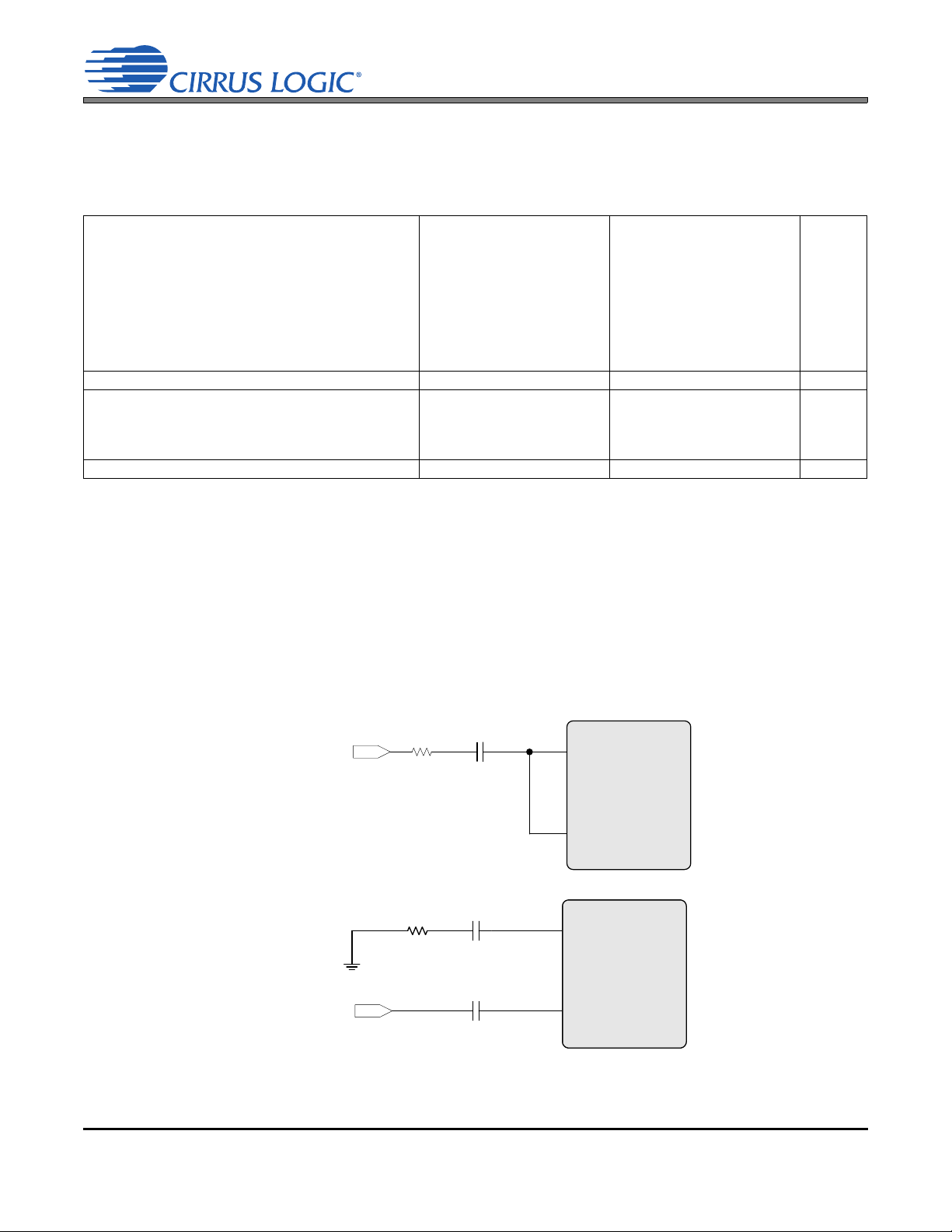
CS42L56
100 mVPP,
25 Hz
100
1 F
AINxA
AINxREF
Figure 4. CMRR Test Configuration
1 µF
AINxx
AINxREF
1 µF
300 mV
PP,
1 kHz
100
Figure 5. AINxREF Input Voltage Test Configuration
ANALOG INPUT CHARACTERISTICS (CONTINUED)
Test Conditions (unless otherwise specified): Connections to the CS42L56 are shown in the “Typical Connection Diagrams” on
page 11; Input test signal is a 1 kHz sine wave through the passive input filter, PGA = 0 dB; All Supplies = VA;
GND = AGND = 0 V; TA=+25C; Measurement bandwidth is 20 Hz to 20 kHz; Sample Frequency = 48 kHz. Measurement sig-
nal path is AINxx to SDOUT.
Full-scale Signal Input Voltage (Note 8)
ADC
0.76•VA
PGA=-1.5 dB, PREAMPx[1:0]=00
PGA=0 dB, PREAMPx[1:0]=00
PGA=+12 dB, PREAMPx[1:0]=00
PGA=0 dB, PREAMPx[1:0]=01
PGA=0 dB, PREAMPx[1:0]=10
PGA=+12 dB, PREAMPx[1:0]=01
PGA=+12 dB, PREAMPx[1:0]=10
AINxREF Input Voltage (Pseudo-Diff Mode)(Note 10) - - 0.300 - - 0.300 Vpp
Input Impedance (Note 9) ADC
PGA, PREAMPx[1:0]=00
PGA, PREAMPx[1:0]=01
PGA, PREAMPx[1:0]=10
DC Voltage at Analog Input (Pin Floating) - VA/2 - - VA/2 - V
0.78•VA
Notes:
5. See Figure 4.
6. SDOUT Code with HPFx=1 and HPFRZx=0.
7. See “Parameter Definitions” on page 91.
8. The full scale input voltage values given in the table refers to the maximum voltage difference between
the AINxx and AINxREF pins. Providing an input signal at these pins that exceeds the full scale input
voltage may result in clipping the analog input.
9. Measured between AINxx and AGND.
10. Providing a signal level higher than 300 mVpp on the AINxREF pin may degrade the PGA linearity and
adversely affect analog input performance. See Figure 5.
-
-
-
-
-
-
-
-
-
-
0.80•VA
0.95•VA
0.82•VA
0.198•VA
0.259•VA
0.082•VA
0.064•VA
0.020•VA
60
40
12.65
4
0.84•VA
-
0.86•VA
-
-
-
-
-
-
-
-
-
0.76•VA
-
0.78•VA
-
-
-
-
-
-
-
-
-
0.80•VA
0.95•VA
0.82•VA
0.198•VA
0.259•VA
0.082•VA
0.064•VA
0.020•VA
60
40
12.65
4
0.84•VA
-
0.86•VA
-
-
-
-
-
-
-
-
-
Vpp
Vpp
Vpp
Vpp
Vpp
Vpp
Vpp
Vpp
k
k
k
k
16 DS851F2
Page 17
CS42L56
ADC DIGITAL FILTER CHARACTERISTICS
Parameter (Note 11) Min Typ Max Unit
Frequency Response (20 Hz to 20 kHz) -0.07 - +0.02 dB
Passband to -0.05 dB corner
to -3 dB corner-Stopband 0.52 - - Fs
Stopband Attenuation 33 - - dB
Total Group Delay - 4.3/Fs - s
High-Pass Filter Characteristics (48 kHz Fs) (Note 12)
Passband to -3.0 dB corner
to -0.05 dB corner-Frequency Response - - 0.15 dB
Phase Deviation @ 20 Hz - 5.3 - Deg
Filter Settling Time (Note 13)
Notes:
11. Response is clock-dependent and will scale with Fs. Note that the response plots (Figures 41 to Note 44
on page 90) have been normalized to Fs and can be denormalized by multiplying the X-axis scale by Fs.
HPF parameters are for Fs = 48 kHz.
12. Characteristics are based on the default setting in register “HPF Control (Address 1Bh)” on page 75.
13. Settling time decreases at higher corner frequency settings.
0.421
0.495
1.87
17.15
10
5
/Fs
-
-
Fs
-
Fs
-
Hz
-
Hz
-s
DS851F2 17
Page 18
CS42L56
HP OUTPUT CHARACTERISTICS
Test conditions (unless otherwise specified): Connections to the CS42L56 are shown in the “Typical Connection Diagrams” on
page 11; Input test signal is a full-scale 997 Hz sine wave; All Supplies = VA, VCP Mode; GND = AGND = 0 V; TA = +25C;
Measurement bandwidth is 20 Hz to 20 kHz; Sample Frequency = 48 kHz; Test load R
and test load R
HPOUTx.
=16 CL = 150 pF for a headphone load (See Figure 6 on page 21); Measurement signal path is SDIN to
L
VA = 2.5 V VA = 1.8 V
Parameter (Note 15)
Line Load RL = 10 k(+2 dB Analog Gain) (Note 14)
Dynamic Range
18 to 24-Bit A-weighted
unweighted
16-Bit A-weighted
unweighted
Total Harmonic Distortion + Noise (Note 16)
18 to 24-Bit 0 dB
-20 dB
-60 dB
16-Bit 0 dB
-20 dB
-60 dB
Full-scale Output Voltage (Note 17)
HP Load RL = 16 (-4 dB Analog Gain) (Note 14)
Dynamic Range
18 to 24-Bit A-weighted
unweighted
16-Bit A-weighted
unweighted
Total Harmonic Distortion + Noise (Note 16)
Full-scale Output Voltage (Note 17)
Output Power (Note 16)
Other Characteristics for RL = 16 or 10 k
Interchannel Isolation 10 k
(Note 17) 16
Interchannel Gain Mismatch (Note 17)
Output Offset Mute
(Note 17) 0 dB Analog Gain
Gain Drift (Note 17)
Load Resistance (R
Load Capacitance (C
) (Note 17)
L
) (Note 17)
L
Min Typ Max Min Typ Max Unit
92
89
-
-
-
-
-
-
-
-
1.56•VA 1.64•VA 1.73•VA 1.56•VA 1.64•VA 1.73•VA V
89
86
-
-
- -75 -69 - -75 -69 dB
0.76•VA 0.82•VA 0.88•VA 0.76•VA 0.82•VA 0.88•VA V
-32- -17-mW
-
-
- 0.1 0.28 - 0.1 0.28 dB
-
-
- ±100 - - ±100 - ppm/°C
16 - - 16 - -
- - 150 - - 150 pF
98
95
96
94
-84
-75
-35
-82
-74
-34
95
92
93
90
90
90
0.5
3.9
±15.1
= 10 k CL=150 pFfor a line load,
L
-
-
-
-
-78
-
-30
-
-
-
-
-
-
-
-
-
1.0
90
87
88
85
96
93
-
-
-
-
-
-
-
-
-
-
-
-
-
-
94
92
-85
-73
-33
-83
-72
-32
94
91
92
89
90
90
0.5
3.1
-
-
-
-
-79
-
-28
-
-
-
-
-
-
-
-
-
1.0
±11.4
dB
dB
dB
dB
dB
dB
dB
dB
dB
dB
PP
dB
dB
dB
dB
PP
dB
dB
mV
mV
18 DS851F2
Page 19
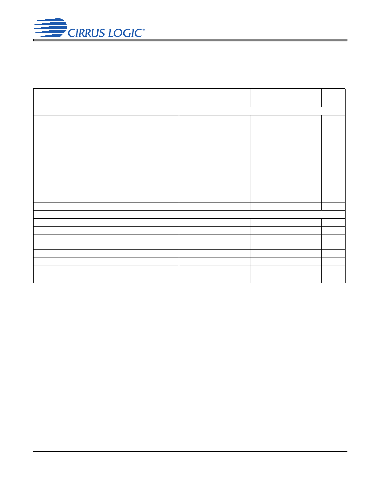
CS42L56
LINE OUTPUT CHARACTERISTICS
Test conditions (unless otherwise specified): Connections to the CS42L56 are shown in the “Typical Connection Diagrams” on
page 11; Input test signal is a full-scale 997 Hz sine wave; All Supplies = VA, VCP Mode; GND = AGND = 0 V; TA = +25C;
Measurement bandwidth is 20 Hz to 20 kHz; Sample Frequency = 48 kHz; Test load R
page 21); Measurement signal path is SDIN to LINEOUTx.
VA = 2.5 V VA = 1 . 8 V
Parameter (Note 15)
(+2 dB Analog Gain) (Note 14)
Dynamic Range
18 to 24-Bit A-weighted
unweighted
16-Bit A-weighted
unweighted
Total Harmonic Distortion + Noise (Note 16)
18 to 24-Bit 0 dB
-20 dB
-60 dB
16-Bit 0 dB
-20 dB
-60 dB
Full-scale Output Voltage (Note 17)
Other Characteristics
Interchannel Isolation (Note 17)
Interchannel Gain Mismatch (Note 17)
Output Offset Mute
(Note 17) 0dB Analog Gain
Gain Drift (Note 17)
Output Impedance
Load Resistance (R
Load Capacitance (CL) (Note 17)
) (Note 17)
L
Min Typ Max Min Typ Max Unit
93
90
-
-
-
-
-
-
-
-
1.50•VA 1.58•VA 1.71•VA 1.50•VA 1.58•VA 1.71•VA V
-90- -90-dB
- 0.1 0.32 - 0.1 0.32 dB
-
-
-±100- -±100-ppm/°C
-100- -100-
10 - - 10 - - k
- - 150 - - 150 pF
99
96
96
94
-84
-76
-36
-82
-74
-34
0.5
3.6
= 10 k CL = 150 pF (see Figure 6 on
L
-
-
-
-
-78
-
-30
-
-
-
1.0
±14.6
91
88
97
94
-
-
-
-
-
-
-
-
-
-
94
92
-86
-74
-34
-84
-72
-32
0.5
2.8
-80
-28
1.0
±10.6
-
-
-
-
-
-
-
-
dB
dB
dB
dB
dB
dB
dB
dB
dB
dB
PP
mV
mV
Notes:
14. The analog gain setting (“Headphone Volume Control” on page 84 or “Line Volume Control” on
page 84) must be configured as indicated to achieve the specified output characteristics.
15. One LSB of triangular PDF dither is added to data.
16. VCP settings lower than VA reduces the headroom of the headphone amplifier. As a result, the specified THD+N performance at full-scale output voltage and power may not be achieved.
17. See Figure 6 and Figure 7. Refer to “Parameter Definitions” on page 91.
18. Response is clock dependent and will scale with Fs. Note that the response plots (Figures 45 to Note 48
on page 90) have been normalized to Fs and can be denormalized by multiplying the X-axis scale by Fs.
19. Measurement bandwidth is from Stopband to 3 Fs.
DS851F2 19
Page 20
CS42L56
Figure 6. HP Output Test Configuration
Test Load
HPOUTx
GND/A GND
C
L
0.1 µF
33
HPREF
R
L
Measurement
Device
-
+
Symbolized component values are specified in table “HP
Output Characteristics” on page 19
Test Load
LINEOUTx
GND/A GND
C
L
LINERE F
R
L
Measurement
Device
-
+
Figure 7. Line Output Test Configuration
Symbolized component values are specified in table “Line
Output Characteristics” on page 20
20 DS851F2
Page 21
CS42L56
ANALOG PASSTHROUGH CHARACTERISTICS
Test Conditions (unless otherwise specified): Connections to the CS42L56 are shown in the “Typical Connection Diagrams” on
page 11; Input test signal is a 1 kHz sine wave through the passive input filter shown in Figure 1, PGA and HP/Line gain = 0 dB;
All Supplies = VA, VCP Mode; GND = AGND = 0 V; T
quency = 48 kHz; Measurement signal path is AINxx to HPOUTx or LINEOUTx.
Parameter
Analog In to HP Amp (ADC is powered down)
R
= 10 k(+2 dB Output Analog Gain) (Note 14)
L
Dynamic Range A-weighted
Total Harmonic Distortion + Noise (Note 16)
Full-scale Input Voltage (Note 8) - 0.80•VA - - 0.80•VA - Vpp
Full-scale Output Voltage (Note 17) - 0.93•VA - - 0.93•VA - Vpp
Frequency Response - 0/-0.3 - - 0/-0.3 - dB
= 16 (-4 dB Output Analog Gain) (Note 14)
R
L
Dynamic Range A-weighted
Total Harmonic Distortion + Noise (Note 16)
-20 dB
Full-scale Input Voltage (Note 8) - 0.80•VA - - 0.80•VA - Vpp
Output Power (Note 16) -12- -6.5-mW
Frequency Response - 0/-0.3 - - 0/-0.3 - dB
Analog In to Line Amp (ADC is powered down)
= 10 k(+2 dB Output Analog Gain) (Note 14)
R
L
Dynamic Range A-weighted
Total Harmonic Distortion + Noise (Note 16)
Full-scale Input Voltage (Note 8) - 0.80•VA - - 0.80•VA - Vpp
Full-scale Output Voltage (Note 17) - 0.89•VA - - 0.89•VA - Vpp
Frequency Response - 0/-0.3 - - 0/-0.3 - dB
= +25C; Measurement bandwidth is 20 Hz to 20 kHz; Sample Fre-
A
VA = 2.5 V VA = 1.8 V
Min Typ Max Min Typ Max Unit
unweighted--
-1 dB
-20 dB
-60 dB
unweighted--
-1 dB
-60 dB
unweighted--
-1 dB
-20 dB
-60 dB
94
91
-
-
-
-
-
-
-
-
-
-70
-71
-31
94
91
-70
-71
-31
94
91
-70
-71
-31
-
-
-
-
-
-
-
-
-
-
-
-
-
-
-
-
-
-
-
-
-
-
-
-
-
-
-
-
-
-
91
88
-80
-68
-28
91
88
-80
-68
-28
91
88
-80
-68
-28
-
dB
-
dB
-
dB
-
dB
-
dB
-
dB
-
dB
-
dB
-
dB
-
dB
-
dB
-
dB
-
dB
-
dB
-
dB
COMBINED DAC INTERPOLATION & ON-CHIP ANALOG FILTER RESPONSE
Parameter (Note 18) Min Typ Max Unit
Frequency Response 20 Hz to 20 kHz Fs = 48.000 kHz
Fs = 44.118 kHz
Passband to -0.05 dB corner
to -3 dB corner
Stopband 0.55 - - Fs
Stopband Attenuation (Note 19) 49 - - dB
Total Group Delay - 6.5/Fs - s
De-emphasis Error Fs = 44.118 kHz - - +0.05/-0.25 dB
DS851F2 21
-0.007
-0.081
-
-
-
-
0.48
0.49
+0.007
+0.081
-
-
dB
dB
Fs
Fs
Page 22
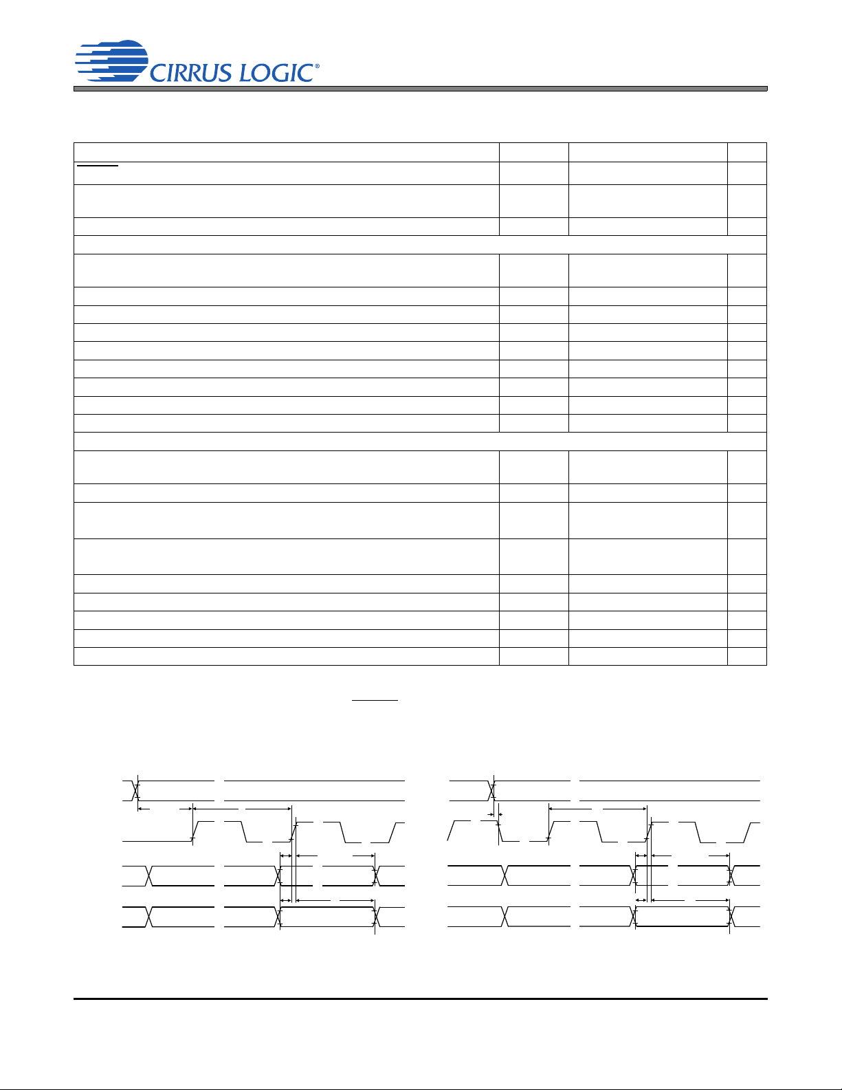
CS42L56
Figure 8. Serial Port Timing (Slave Mode) Figure 9. Serial Port Timing (Master Mode)
t
hs(SK-SDO)
//
//
//
//
//
//
//
//
t
ss(SD-SK)
MSB
MSB
LRCK
SCLK
SDOUT
SDIN
t
ss(LK-SK)
t
P
t
hs
t
ss(SDO-SK)
//
//
//
//
t
hm(SK-SDO)
//
//
//
//
//
//
//
//
t
sm(SD-SK)
MSB
MSB
LRCK
SCLK
SDOUT
SDIN
t
Pm
t
hm
t
sm(SDO-SK)
//
//
//
//
//
//
t
sm(LK-SK)
SWITCHING SPECIFICATIONS - SERIAL PORT
Inputs: Logic 0 = GND = AGND, Logic 1 = VL, LRCK, SCLK, SDOUT C
Parameters Symbol Min Max Units
RESET pin Low Pulse Width (Note 20) 1-ms
MCLK Frequency
MCLK Duty Cycle 45 55 %
Slave Mode (Figure 8)
Input Sample Rate (LRCK) F
LRCK Duty Cycle 45 55 %
SCLK Frequency 1/t
SCLK Duty Cycle 45 55 %
LRCK Setup Time Before SCLK Rising Edge t
SDOUT Setup Time Before SCLK Rising Edge t
SDOUT Hold Time After SCLK Rising Edge t
SDIN Setup Time Before SCLK Rising Edge t
SDIN Hold Time After SCLK Rising Edge t
Master Mode (Figure 9)
Output Sample Rate (LRCK)
LRCK Duty Cycle 45 55 %
SCLK Frequency SCLK = MCLK mode 1/t
All Other Modes 1/t
SCLK Duty Cycle RATIO[4:0] = ‘xxx00’ or ‘xxx11’ 45 55 %
RATIO[4:0] = ‘xxx01’ (Note 21) 33 66 %
LRCK Time Before SCLK Falling Edge t
SDOUT Setup Time Before SCLK Rising Edge t
SDOUT Hold Time After SCLK Rising Edge t
SDIN Setup Time Before SCLK Rising Edge t
SDIN Hold Time After SCLK Rising Edge t
LOAD
= 15 pF.
ss(LK-SK)
ss(SDO-SK)
hs(SK-SDO)
ss(SD-SK)
hs
F
sm(LK-SK)
sm(SDO-SK)
hm(SK-SDO)
sm(SD-SK)
hm
s
Ps
s
Pm
Pm
(See “Serial Port Clocking”
on page 47)
(See “Serial Port Clocking”
on page 47)
MHz
kHz
-68•FsHz
40 - ns
20 - ns
30 - ns
20 - ns
20 - ns
(See “Serial Port Clocking”
on page 47)
Hz
- 12.0000 MHz
-68•FsHz
-±2ns
20 - ns
30 - ns
20 - ns
20 - ns
Notes:
20. After powering up the CS42L56, RESET
should be held low after the power supplies and clocks are
settled. This specification is valid with the recommended capacitor on VDFILT.
21. When the RATIO[1:0] = ‘01’, the device will periodically extend the SCLK high time to compensate for
the resulting fractional MCLK/SCLK ratio.
22 DS851F2
Page 23
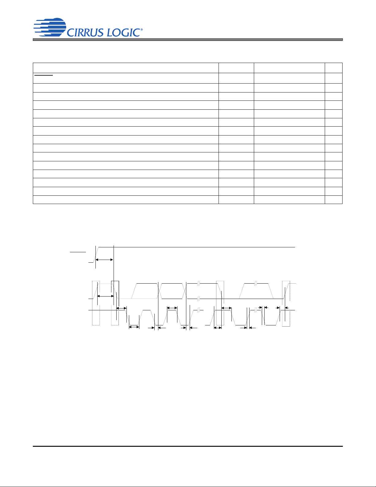
SWITCHING SPECIFICATIONS - I²C CONTROL PORT
t
buf
t
hdst
t
hdst
t
low
t
r
t
f
t
hdd
t
high
t
sud
t
sust
t
susp
Stop Start
Start
Stop
Repeated
SDA
SCL
t
irs
RESET
Figure 10. I²C Control Port Timing
Inputs: Logic 0 = GND = AGND, Logic 1 = VL (Note 22) .
Parameter Symbol Min Max Unit
CS42L56
RESET Rising Edge to Start t
SCL Clock Frequency f
Start Condition Hold Time (prior to first clock pulse) t
Clock Low Time t
Clock High Time t
Setup Time for Repeated Start Condition t
SDA Input Hold Time from SCL Falling (Note 23) t
SDA Output Hold Time from SCL Falling t
SDA Setup Time to SCL Rising t
Rise Time of SCL and SDA t
Fall Time SCL and SDA t
Setup Time for Stop Condition t
Bus Free Time Between Transmissions t
SDA Bus Capacitance C
SDA Pull-Up Resistance R
Notes:
22. All specifications are valid for the signals at the pins of the CS42L56 with the specified load capacitance.
23. Data must be held for sufficient time to bridge the transition time, t
irs
scl
hdst
low
high
sust
hddi
hddo
sud
rc
fc
susp
buf
L
p
, of SCL.
f
500 - ns
- 550 kHz
0.6 - µs
1.3 - µs
0.6 - µs
0.6 - µs
00.9µs
0.2 0.9 µs
100 - ns
-300ns
-300ns
0.6 - µs
1.3 - µs
-400pF
500 -
DS851F2 23
Page 24
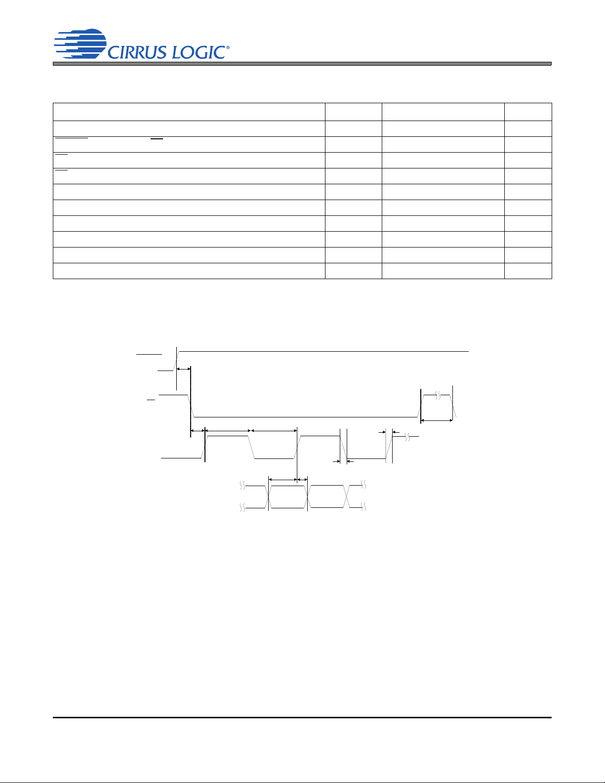
SWITCHING CHARACTERISTICS - SPI CONTROL PORT
CS
CCLK
CDIN
RESET
t
srs
t
scl
t
sch
t
css
t
r2
t
f2
t
csh
t
dsu
t
dh
Figure 11. Control Port Timing - SPI Format
Inputs: Logic 0 = GND = AGND, Logic 1 = VL, SDA CL=30pF.
Parameter Symbol Min Max Units
CCLK Clock Frequency
RESET Rising Edge to CS Falling
Falling to CCLK Edge
CS
CS High Time Between Transmissions
CCLK Low Time
CCLK High Time
CDIN to CCLK Rising Setup Time
CCLK Rising to DATA Hold Time (Note 24)
Rise Time of CCLK and CDIN (Note 25)
Fall Time of CCLK and CDIN (Note 25)
Notes:
24. Data must be held for sufficient time to bridge the transition time of CCLK.
25. For f
<1 MHz.
sck
f
t
t
t
t
t
sck
srs
css
csh
t
sch
dsu
t
t
t
scl
dh
20 - ns
20 - ns
1.0 - s
66 - ns
66 - ns
40 - ns
15 - ns
r2
f2
CS42L56
06.0MHz
- 100 ns
- 100 ns
24 DS851F2
Page 25
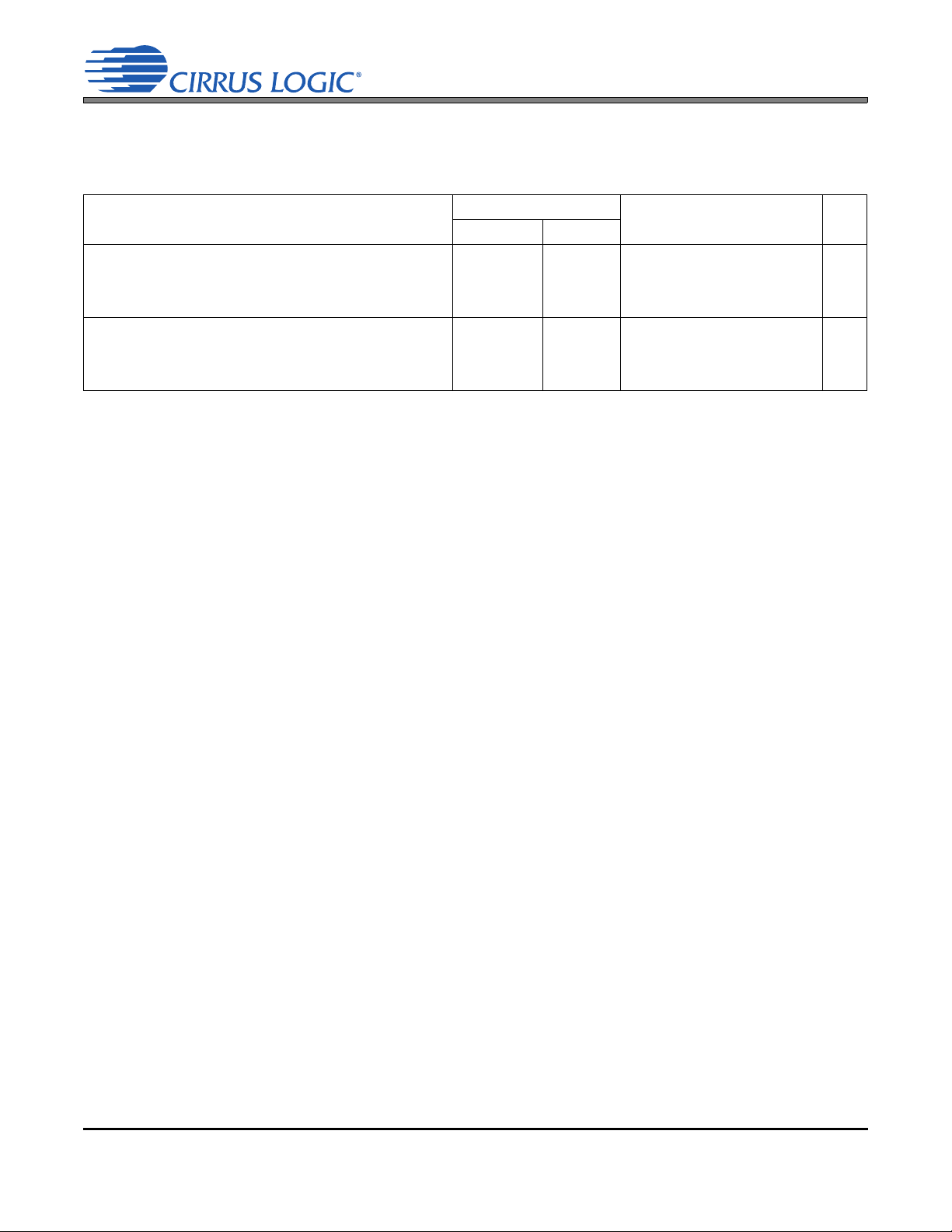
CS42L56
ANALOG OUTPUT ATTENUATION CHARACTERISTICS
Test Conditions (unless otherwise specified): Connections to the CS42L56 are shown in the “Typical Connection Diagrams” on
page 11; GND = AGND = 0 V. Attenuation is referenced to the full-scale voltage for the given output. Test load RL = 3 k
= 150 pFfor a line load, and test load RL=16 CL = 150 pF for a headphone load (See Figure 6 and Figure 7 on page 21).
C
L
Power Status
Parameters
Headphone Mute Attenuation (HPxMUTE=1) (Note 26)
Line Mute Attenuation (LINExMUTE=1) (Note 26)
Notes:
26. Assumes no external impedance on HPREF or LINEREF. External impedance on HPREF or LINEREF
will impact the attenuation.
Headphone Line
OFF
OFF
ON
ON
OFF
OFF
ON
ON
OFF
ON
OFF
ON
OFF
ON
OFF
ON
Min Typ Max Units
-
-
-
-
-
-
-
-
90
90
90
90
90
90
90
90
-
-
-
-
-
-
-
-
dB
dB
dB
dB
dB
dB
dB
dB
DS851F2 25
Page 26
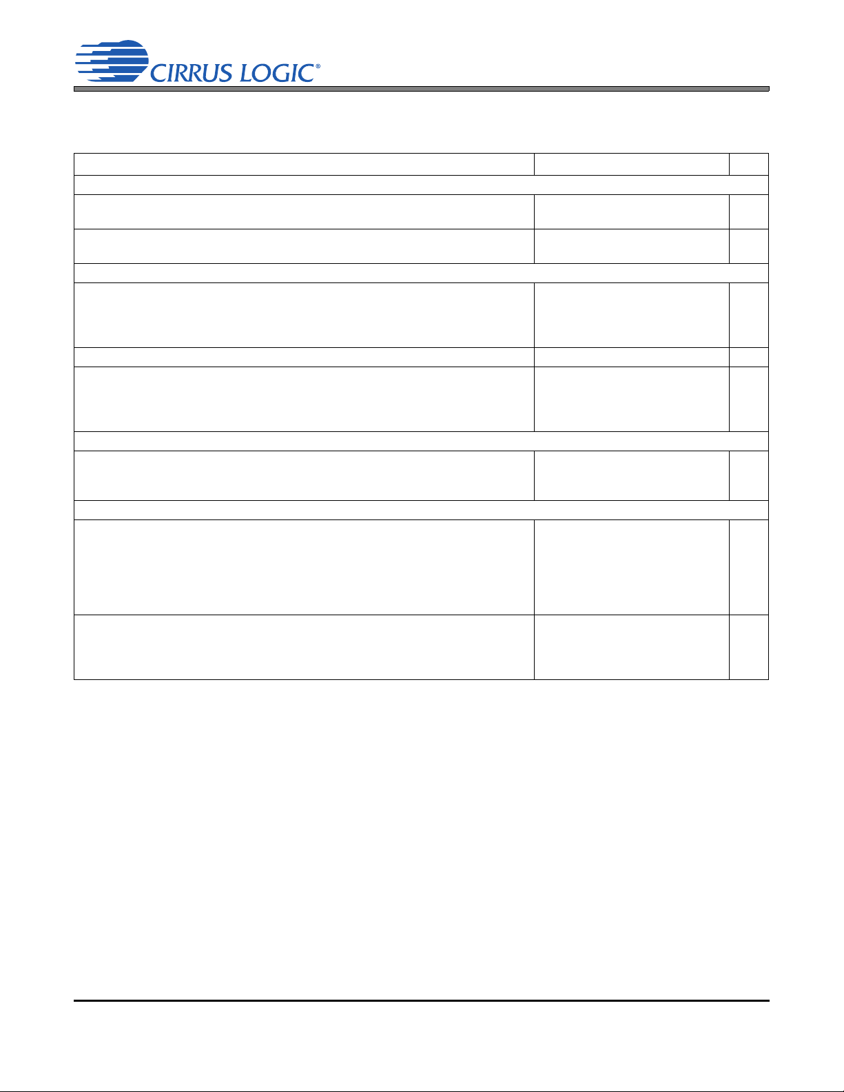
CS42L56
DC CHARACTERISTICS
Test Conditions (unless otherwise specified): Connections to the CS42L56 are shown in the “Typical Connection Diagrams” on
page 11; GND = AGND = 0 V; all voltages with respect to ground.
Parameters Min Typ Max Units
VHPFILT Characteristics (Note 27)
VCP Mode +VHPFILT
-VHPFILT
VCP/2 Mode +VHPFILT
-VHPFILT
MIC BIAS Characteristics
Nominal Voltage BIAS_LVL[1:0] = 00
BIAS_LVL[1:0] = 01
BIAS_LVL[1:0] = 10
BIAS_LVL[1:0] = 11
DC Output Current (Note 28) - - 1.22 mA
Power Supply Rejection Ratio (PSRR) @ 1 kHz BIAS_LVL[1:0] = 00
BIAS_LVL[1:0] = 01
BIAS_LVL[1:0] = 10
BIAS_LVL[1:0] = 11
Misc. DC Filter Characteristics
FILT+
VQ
VDFILT
Power Supply Rejection Ratio (PSRR) Characteristics
PSRR with 100 mVpp, 1 kHz signal (Note 29) PGA to ADC
PGA (Pseudo Differential) to ADC
ADC
PGA to HP & Line Amps
PGA (Pseudo Differential) to HP & Line Amps
DAC to HP & Line Amps
P
SRR with 100 mVpp, 60 Hz signal (Notes 29, 30) PGA to ADC
ADC
PGA to HP & Line Amps
DAC to HP & Line Amps
-
-
-
-
-
-
-
-
-
-
-
-
-
-
-
-
-
-
-
-
-
-
-
-
-
VCP
-VCP
VCP/2
-VCP/2
0.9•VA
0.8•VA
0.7•VA
0.6•VA
45
50
50
50
VA
VA/ 2
0.9
47
58
57
44
54
56
35
25
50
60
-
-
-
-
-
-
-
-
-
-
-
-
-
-
-
-
-
-
-
-
-
-
-
-
-
V
V
V
V
V
V
V
V
dB
dB
dB
dB
V
V
V
dB
dB
dB
dB
dB
dB
dB
dB
dB
dB
Notes:
27. No load connected to HPOUTx and LINEOUTx.
28. VA = 2.71 V, BIAS_LVL[1:0] = 00, total equivalent external impedance to ground = 2 k.
29. Valid with the recommended capacitor values on FILT+ and VQ, no load on HP and Line. Increasing
the capacitance on FILT+ and VQ will also increase the PSRR.
30. The PGA is biased with VQ, created by a resistor divider from the VA supply. Increasing the capacitance
on FILT+ and VQ will also increase the PSRR at low frequencies. A 10 µF capacitor on VQ improves
the PSRR to 42 dB.
26 DS851F2
Page 27
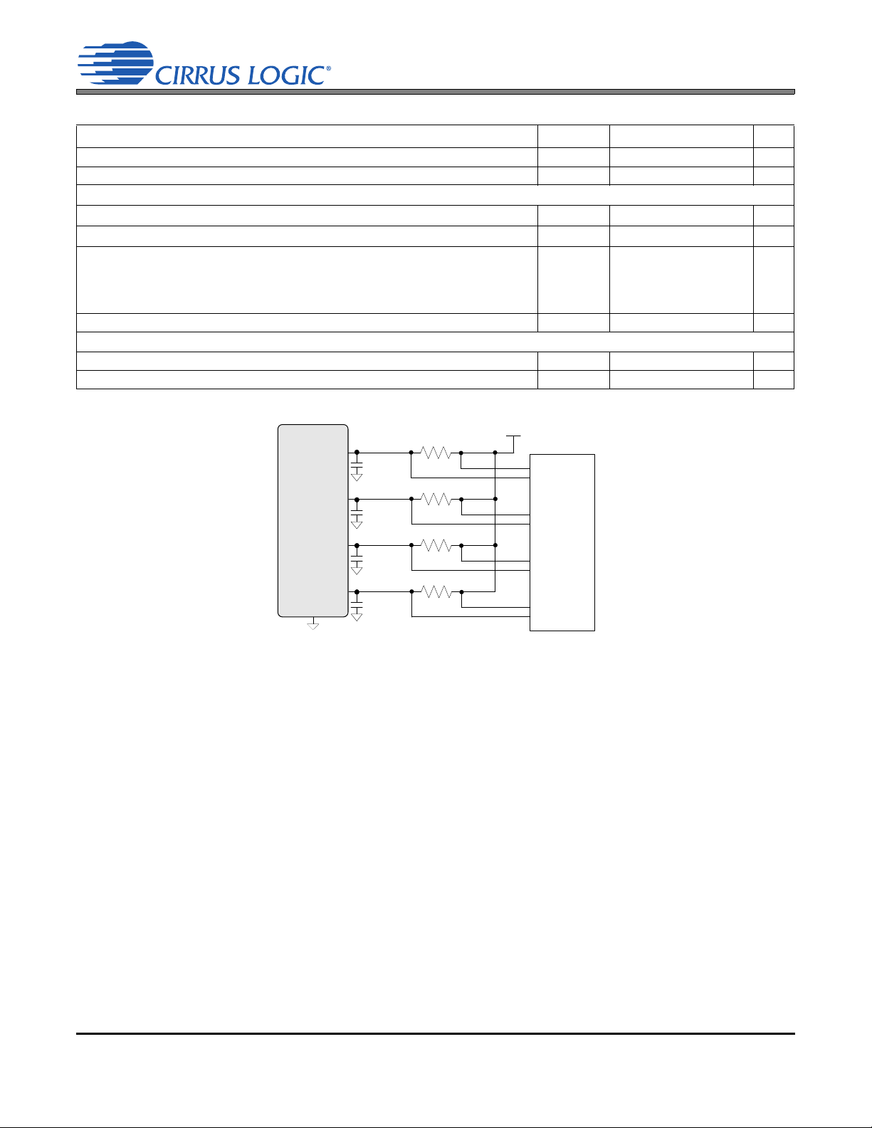
CS42L56
VCP
GND/AGND
Voltmeter
-
+
1
Power Supply
-
+
1
-
+
1
-
+
1
VA
VLDO
VL
2.2 µF
0.1 µF
0.1 µF
0.1 µF
Note: Current is derived from the voltage drop across
a 1 resistor in series with each supply input.
Figure 12. Power Consumption Test Configuration
DIGITAL INTERFACE SPECIFICATIONS & CHARACTERISTICS
Parameters (Note 31) Symbol Min Max Units
Input Leakage Current I
in
Input Capacitance -10pF
1.8 V - 3.3 V Logic
High-Level Output Voltage (I
Low-Level Output Voltage (I
= -100 A) V
OH
= 100 A) V
OL
OH
OL
High-Level Input Voltage VL = 1.65 V
VL = 1.8 V
VL = 2.0 V
V
IH
VL > 2.0 V
Low-Level Input Voltage V
IL
HPDETECT Input
High-Level Input Voltage HPDV
Low-Level Input Voltage HPDV
IH
IL
31. See “I/O Pin Characteristics” on page 10 for serial and control port power rails.
-±10A
VL - 0.2 - V
-0.2V
0.83•VL
0.76•VL
0.68•VL
0.65•VL
-
V
-
-
-
-0.30•VLV
0.65•VA - V
- 0.35•VA V
DS851F2 27
Page 28
POWER CONSUMPTION - ALL SUPPLIES = 1.8 V
Power Ctl. Registers ADC, Line, HP
Sel. Registers
Operation Test Conditions (unless otherwise
specified): All zeros input,
slave mode, sample rate =
48 kHz; No load. Refer to
Figure 12 on page 28.
1
Off (Note 32)
Standby (Note 33) MCLKDIS=1
2
MCLKDIS=0
(Note 34) MCLKDIS=x
Mono Record (Note 35) ADC
3
PGA to ADC
Stereo Record (Note 35) ADC
4
PGA to ADC
Mono Play to HP No Effects
5
Mono Play to Line No Effects
6
Stereo Play to HP No Effects
7
Stereo Play to Line No Effects
8
Stereo Passthrough to HP
9
Stereo Passthrough to Line
10
Mono Rec. & Play No Effects
11
PGA In, HP Out
Stereo Rec. & Play No Effects
12
PGA In, HP Out
Stereo Play to HP No Effects
13
16 load (Note 36)
02h
page 58
PDN_CHRG
PDN_ADCB
03h page 59 08h page 74
PDN_ADCA
PDN
PDN_HPB[1:0]
PDN_HPA[1:0]
PDN_LINB[1:0]
PDN_LINA[1:0]
ADCBMUX[1:0]
ADCAMUX[1:0]
xxxxx x x x x x xxxxx
xxx1x x x x x x xxxxx
xxx1x x x x x x xxxxx
xxx1x x x x x x xxxxx
010011111111xx01xxxxx
010011111111xx00xxxxx
0000111111110101xxxxx
0000111111110000xxxxx
111011101111xxxxxxx01
Effects
111011101111xxxxxxx00
111011111110xxxxx0xx1
Effects
111011111110xxxxx0xx0
111010101111xxxxxx001
Effects
111010101111xxxxxx000
111011111010xxxx00xx1
Effects
111011111010xxxx00xx0
011010101111xxxxxx11x
011011111010xxxx11xxx
010011101111xx00xxx01
010011101111xx00xxx00
Effects
0000101011110000xx001
Effects
0000101011110000xx000
111010101111xxxxxx001
LINEBMUX
LINEAMUX
HPBMUX
HPAMUX
CS42L56
Typical Current (mA)
i
VCPiVAiVLDOiVL
Class
H
Mode
page
63
PDN_DSP - 0Fh page 66
- 0.001 0.001 0.007 0.002 0.02
- 0.001 0.001 0.053 0.007 0.11
- 0.001 0.010 0.292 0.007 0.56
- 0.001 0.001 0.020 0.001 0.04
- 0.001 0.915 0.671 0.018 2.89
- 0.001 1.056 0.672 0.017 3.14
- 0.001 1.207 0.824 0.023 3.70
- 0.002 1.469 0.826 0.022 4.17
VCP/2
0.407 1.100 0.718 0.007 4.02
VCP
0.949 1.107 0.718 0.007 5.01
VCP/2
0.407 1.100 1.050 0.007 4.62
VCP
0.948 1.107 1.050 0.007 5.60
VCP/2
0.392 1.101 0.719 0.007 3.99
VCP
0.844 1.107 0.717 0.007 4.82
VCP/2
0.392 1.101 1.046 0.007 4.58
VCP
0.844 1.107 1.046 0.007 5.41
VCP/2
0.604 1.587 0.720 0.007 5.25
VCP
1.420 1.594 0.717 0.007 6.73
VCP/2
0.604 1.587 1.090 0.007 5.92
VCP
1.419 1.594 1.090 0.007 7.40
VCP/2
0.570 1.589 0.718 0.007 5.19
VCP
1.205 1.597 0.719 0.007 6.35
VCP/2
0.570 1.589 1.089 0.007 5.86
VCP
1.205 1.597 1.088 0.007 7.01
VCP/2
0.565 1.180 0.213 0.007 3.54
VCP
1.198 1.188 0.213 0.007 4.69
VCP/2
0.571 1.183 0.213 0.007 3.55
VCP
1.205 1.190 0.213 0.007 4.71
VCP/2
0.408 1.921 1.084 0.018 6.18
VCP
0.950 1.928 1.089 0.018 7.17
VCP/2
0.408 1.921 1.415 0.018 6.77
VCP
0.952 1.928 1.412 0.018 7.76
VCP/2
0.604 2.820 1.239 0.023 8.43
VCP
1.422 2.827 1.240 0.023 9.92
VCP/2
0.604 2.820 1.613 0.023 9.11
VCP
1.424 2.827 1.612 0.023 10.59
VCP/2
2.725 1.579 0.737 0.008 9.09
Tota l
Power
(mW)
28 DS851F2
Page 29

POWER CONSUMPTION - ALL SUPPLIES = 2.5 V
CS42L56
Operation Test Conditions
(unless otherwise specified):
All zeros input, slave mode,
sample rate = 48 kHz; No
load. Refer to Figure 12 on
page 28.
1
Off (Note 32)
Standby (Note 33) MCLKDIS=1
2
MCLKDIS=0 xxx1x x x x x x xxxxx
(Note 34) MCLKDIS=x xxx1x x x x x x xxxxx
Mono Record (Note 35) ADC
3
PGA to ADC
Stereo Record (Note 35) ADC
4
PGA to ADC
Mono Play to HP No Effects
5
Effects
Mono Play to Line No Effects
6
Stereo Play to HP No Effects
7
Effects
Effects
Stereo Play to Line No Effects
8
Effects 111011111010xxxx00xx0
Stereo Passthrough to HP
9
Stereo Passthrough to Line
10
Mono Rec. & Play No Effects
11
PGA In, HP Out
Effects
Stereo Rec. & Play No Effects
12
PGA In, HP Out
Effects
Stereo Play to HP No Effects
13
16 load (Note 36)
Notes:
32. RESET
33. RESET
pin and clock/data lines held LO, PDN=x.
pin held HI, PDN=1.
34. Clock/data lines held HI.
35. Either inputs 1 or 2 may be selected. Input 1 is shown for simplicity.
36. In accordance with the JEITA CP-2905B standard, 0.1 mW (per channel) is delivered to the headphone load.
Power Ctl. Registers MUX Registers
02h
page 58
PDN_CHRG
PDN_ADCB
xxxxx x x x x x xxxxx
xxx1x x x x x x xxxxx
110011111111xx01xxxxx
110011111111xx00xxxxx
1000111111110101xxxxx
1000111111110000xxxxx
111011101111xxxxxxx01
111011101111xxxxxxx00
111011111110xxxxx0xx1
111011111110xxxxx0xx0
111010101111xxxxxx001
111010101111xxxxxx000
111011111010xxxx00xx1
111010101111xxxxxx11x
111011111010xxxx11xxx
110011101111xx00xxx01
110011101111xx00xxx00
1000101011110000xx001
1000101011110000xx000
111010101111xxxxxx001
03h page 59 08h page 74
PDN_ADCA
PDN
PDN_HPB[1:0]
PDN_HPA[1:0]
PDN_LINB[1:0]
PDN_LINA[1:0]
ADCBMUX[1:0]
ADCAMUX[1:0]
LINEBMUX
LINEAMUX
HPBMUX
PDN_DSP - 0Fh page 66
HPAMUX
Typical Current (mA)
i
VCPiVAiVLDOiVL
Class
H
Mode
page
63
-
-
-
-
-
-
-
-
VCP/2
VCP
VCP/2
VCP
VCP/2
VCP
VCP/2
VCP
VCP/2
VCP
VCP/2
VCP
VCP/2
VCP
VCP/2
VCP
VCP/2
VCP
VCP/2
VCP
VCP/2
VCP
VCP/2
VCP
VCP/2
VCP
VCP/2
VCP
VCP/2
0.002 0.013 0.004 0.05
0.002
0.003 0.084 0.012 0.26
0.003
0.017 0.466 0.012 1.25
0.003
0.003 0.032 0.003 0.10
0.003
0.789 0.744 0.026 3.91
0.003
0.963 0.748 0.026 4.35
0.003
1.089 0.919 0.033 5.11
0.003
1.419 0.922 0.033 5.94
0.003
1.469 0.734 0.012 7.35
0.723
1.480 0.736 0.012 10.53
1.984
1.468 1.071 0.012 8.19
0.723
1.480 1.069 0.012 11.36
1.982
1.469 0.736 0.012 7.28
0.693
1.481 0.732 0.012 10.11
1.819
1.469 1.073 0.012 8.12
0.693
1.481 1.069 0.012 10.95
1.819
2.099 0.737 0.012 9.46
0.936
2.113 0.736 0.012 13.48
2.530
2.099 1.109 0.012 10.39
0.934
2.113 1.109 0.012 14.40
2.526
2.102 0.737 0.012 9.31
0.873
2.115 0.736 0.012 12.65
2.197
2.102 1.110 0.012 10.24
0.873
2.115 1.108 0.012 13.58
2.196
1.203 0.228 0.012 5.78
0.870
1.218 0.228 0.012 9.15
2.202
1.206 0.228 0.012 5.80
0.874
1.220 0.228 0.012 9.14
2.196
2.148 1.157 0.026 10.14
0.723
2.160 1.162 0.026 13.32
1.981
2.148 1.491 0.026 10.97
0.723
2.160 1.489 0.027 14.15
1.983
3.233 1.335 0.033 13.84
0.936
3.247 1.336 0.033 17.87
2.532
3.233 1.710 0.033 14.78
0.936
3.247 1.710 0.033 18.81
2.534
3.032 2.081 0.754 0.012 14.70
Total
Power
(mW)
DS851F2 29
Page 30

4. APPLICATIONS
4.1 Overview
4.1.1 Basic Architecture
The CS42L56 is a highly integrated, ultra-low power, 24-bit audio CODEC comprised of stereo A/D and
D/A converters with pseudo-differential stereo input and output amplifiers. The ADC and DAC are designed using multi-bit delta-sigma techniques; both converters operate at a low oversampling ratio of
64xFs, maximizing power savings while maintaining high performance. The CODEC accepts and is capable of generating serial audio clocks (SCLK, LRCK) derived from a USB or a standard audio input Master Clock (MCLK). Designed with a very low voltage digital core and low voltage Class H amplifiers
(powered from an integrated low-dropout regulator and a step-down/inverting charge pump, respectively),
the CS42L56 provides significant reduction in overall power consumption.
4.1.2 Line Inputs
The analog input portion of the CODEC allows selection from up to three stereo line-level sources into a
Programmable Gain Amplifier (PGA). The optional line pseudo-differential configuration provides common-mode noise rejection for single-ended inputs and is available on AIN1x or AIN2x. If pseudo-differential operation is not required, the pins can also be configured independently as two additional analog
inputs (AIN3x).
CS42L56
4.1.3 Line and Headphone Outputs (Class H, Ground-Centered Amplifiers)
The analog output portion of the CODEC includes separate pseudo-differential headphone and line out
Class H amplifiers. An on-chip step-down/inverting charge pump creates a positive and negative voltage
equal to the input or one-half the input supply for the amplifiers, allowing an adaptable, full-scale output
swing centered around ground. The inverting architecture eliminates the need for large DC-blocking capacitors and allows the amplifier to deliver more power to headphone loads at lower supply voltages. The
step-down architecture allows the amplifier’s power supply to adapt to the required output signal. This
adaptive power supply scheme converts traditional Class AB amplifiers into more power-efficient Class H
amplifiers.
4.1.4 Fixed-function DSP Engine
The fixed function digital signal processing engine processes both the PCM serial input data and ADC
output data allowing a mix between the two. Independent volume control, left/right channel swaps, mono
mixes, tone control comprise the DSP engine.
4.1.5 Beep Generator
The beep generator delivers tones at select frequencies across approximately two octave major scales.
With independent volume control, beeps may be configured to occur continuously, periodically or at single
time intervals.
4.1.6 Power Management
Several control registers and bits provide independent power down control of the ADC, PGA, DSP, headphone and line outputs, allowing operation in select applications with minimal power consumption.
30 DS851F2
Page 31

4.2 Analog Inputs
`
Gain Adjust
ALC
PDN_ADCA
PGAAVOL[5:0]
PGAB=A
ANLGZC
HPFRZA
HPFA
HPFA_CF[1:0]
PDN_ADCA
INV_ADCA
PDN_CHRG
ALCB
ALCBSRDIS
ALCBZCDIS
PCM Serial Interface
TO DSP Engine
ALCARATE[5:0]
ALCRRATE[5:0]
ALCMAX[2:0]
ALCMIN[2:0]
ALCA
ALCASRDIS
ALCAZCDIS
AIN1A
AIN2A
ADC
PDN_ADCB
PGABVOL[5:0]
PGAB=A
ANLGZC
BOOSTB
ADCBMUTE
DIGSFT
ADCBATT[7:0]
ADCB=A
HPFRZB
HPB
HPFB_CF[1:0]
PDN_ADCB
INV_ADCB
PDN_CHRG
Noise Gate
NGALL
NG
THRESH[3:0]
NGDELAY[1:0]
Gain Adjust
FROM DSP ENGINE
DIGMUX
ANALOG PASSTHRU TO
HEADPHONE, LINE AMPLIFIER MUX
Swap/
Mix
DIGSUM[1:0]
BOOSTA
ADCAMUTE
DIGSFT
ADCAATT[7:0]
ADCB=A
ADC
ADCAMUX[1:0]
AIN2REF
/ AIN3B
PGAAMUX[1:0]
PREAMPA[1:0]
AIN1B
AIN2B
ADCBMUX[1:0]
AIN1REF
/ AIN3A
AIN1A_REF
AIN2A_REF
PGA A
PGABMUX[1:0]
PREAMPB[1:0]
AIN1B_REF
AIN2B_REF
PGA B
VQ
Figure 13. Analog Input Signal Flow
CS42L56
Referenced Control Register Location
Analog Front End
AIN1x_REF
AIN2x_REF
PREAMPx[1:0]
PGAxMUX[1:0]
PDN_ADCx
PGAxVOL[5:0]
PGAB=A
ANLGZCx
ADCxMUX[1:0]
INV_ADCx
PDN_CHRG
HPFRZx
HPFx
HPFx_CF[1:0]
Digital Volume
BOOSTx
ADCxMUTE
ADCxATT[7:0]
DIGSFT
ADCB=A
ALCx
ALCxSRDIS
ALCxZCDIS
ALCARATE[5:0]
ALCRRATE[5:0]
MAX[2:0]
MIN[2:0]
NGALL
NG
THRESH[3:0]
NGDELAY[1:0]
Miscellaneous
DIGSUM[1:0]
DIGMUX
DS851F2 31
“Analog Input 1 x Reference Configuration” on page 74
“Analog Input 2 x Reference Configuration” on page 74
“PGA x Preamplifier Gain” on page 77
“PGA x Input Select” on page 77
“Power Down ADC x” on page 59
“PGAx Volume” on page 78
“PGA Channel B=A” on page 76
“Analog Zero Cross” on page 64
“ADC x Input Select” on page 75
“Invert ADC Signal Polarity” on page 76
“Power Down ADC Charge Pump” on page 59
“ADCx High-Pass Filter Freeze” on page 75
“ADCx High-Pass Filter” on page 75
“HPF x Corner Frequency” on page 75
“Boostx” on page 77
“ADC Mute” on page 76
“ADCx Volume” on page 78
“Digital Soft Ramp” on page 64
“ADC Channel B=A” on page 76
“ALCx” on page 79
“ALCx Soft Ramp Disable” on page 82
“ALCx Zero Cross Disable” on page 82
“ALC Attack Rate” on page 79
“ALC Release Rate” on page 80
“ALC Maximum Threshold” on page 80
“ALC Minimum Threshold” on page 81
“Noise Gate All Channels” on page 81
“Noise Gate Enable” on page 81
“Noise Gate Threshold and Boost” on page 82
“Noise Gate Delay Timing” on page 82
“Digital Sum” on page 76
“Digital MUX” on page 63
Page 32

4.2.1 Pseudo-differential Inputs
xIN
xREF
Signal+
Anti-
Aliasing
Filter
Common-Mode Cancellation,
Invert, and Gain
AFILTx
DC-Block
VA
VQ
AGND
VCM
R
R
ADC
Parallel PCB
traces from
signal source
Digital
Full Scale
VCM
VCM
V=?
VCM
VCM
-
+
-
+
Figure 14. Stereo Pseudo-Differential Input
The CS42L56 implements a pseudo-differential input stage. The AINxREF inputs are intended to be used
as a pseudo-differential reference signal. This feature provides common mode noise rejection with singleended signals. Figure 14 shows a basic diagram outlining the internal implementation of the pseudo-differential input stage, including a recommended stereo pseudo-differential input topology. If pseudo-differential input functionality is not required, the AINxREF pin should be AC-coupled to GND.
CS42L56
It should be noted that the AINxREF inputs are intended to be used solely to provide a low-level, pseudodifferential reference signal for the internal input amplifiers when in pseudo-differential mode. Using the
analog input pins in a fully differential configuration by providing a large signal on the AINxREF pin is not
recommended. The output of the PGA will clip if the voltage difference between AINxx and AINxREF exceeds the full-scale voltage specification (See Note 10 on page 17).
4.2.2 Large-scale Inputs
The CS42L56 allows the user to input signals that would be larger than the ADC full-scale input voltage
by using the PGA to attenuate the signal prior to going to the ADC. Table 1 shows the PGA gain setting
needed to stay under the maximum ADC input voltage.
Supply Voltage PGA Gain Setting Maximum Input Voltage
(V) (dB)
1.8
2.5
32 DS851F2
0.0 509 1.44
-0.5 539 1.52
-1.0 571 1.62
-1.5 604 1.71
0.0 707 2.00
-0.5 748 2.12
-1.0 793 2.24
-1.5 840 2.38
Table 1. Input Voltage PGA Settings
(mV
)(V
RMS
PP
)
Page 33

CS42L56
Figure 15. Analog Input Attenuation
AINxx
Input
R1
R2
1µF
R3
R1 R 2
R1 R 2+
------------------------ -
R2 R 3
R1 R 2 R 2 R 3 R1 R 3++
------------------------------------------------------------------------------
R1 R 3 R 2 R 3+
R1 R 2 R 3++
---------------------------------------------------
AINxx
Input
Figure 16. Example Analog Input Attenuation
7.87 k
4.75 k
1µF
R3
If signals larger than what is shown in Table 1 are needed, an external resistor divider should be used as
shown in Table 15. When using an external resistor divider, the PGA must be configured to be in-circuit.
Three parameters determine the values of resistors R1 and R2 as shown in Figure 15: source impedance,
attenuation, and input impedance. Table 2 shows the design equation used to determine these values.
• Source Impedance: Source impedance is defined as the impedance as seen from the PGA looking
back into the signal network. The PGA achieves optimal THD+N performance with a source impedance less than 5 k.
• Attenuation: The required attenuation factor depends on the magnitude of the input signal. The fullscale input voltage is specified under “Analog Input Characteristics” on page 14. The user should se-
lect values for R1 and R2 such that the magnitude of the incoming signal multiplied by the attenuation
factor is less than or equal to the full-scale input voltage of the device.
• Input Impedance: Input impedance is the impedance from the signal source to the PGA analog input
pins, including the PGA. The PGA’s input impedance (R3 in Figure 15, Table 2, and Figure 16) is given in the “Analog Input Characteristics” on page 14.
Source Impedance
Attenuation Factor
Input Impedance
Table 2. Analog Input Design Parameters
Figure 16 illustrates an example configuration with the PGA in-circuit using one 7.87 kresistor for R1
and one 4.75 k resistor for R2. Based on the discussion above, this circuit provides an optimal interface
for both the PGA and the signal source. First, consumer equipment frequently requires an approximate
input impedance of 10 kwhich the combination of the resistors provide. Second, this circuit will attenuate a typical line level voltage, 2 Vrms, to the full-scale input of the PGA, 0.7 Vrms when VA = 2.5 V. Finally, at approximately 3 kthe source impedance is within the allowable range of the PGA.
DS851F2 33
Page 34

4.2.3 Microphone Inputs
fc
1
2 4 k 1 F
-------------------------------------------- 39.79 Hz==
MICx+
MICx-
+
+
MICBIAS
//
//
Figure 17. MIC Input Mix w/Common Mode Rejection
Any of the line inputs can be configured as a microphone input by using the MICBIAS pin to power the
external microphone circuit and by configuring the additional +10 or +20 dB gain in the PGA to properly
boost the low-level microphone signal.
4.2.3.1 External Passive Components
The analog inputs are internally biased to VQ. Input signals must be AC coupled using external capacitors
with values consistent with the desired high-pass filter design. The analog input resistance may be combined with an external capacitor to achieve the desired cutoff frequency. The equation below gives an example:
An electrolytic capacitor must be placed such that the positive terminal is positioned relative to the side
with the greater bias voltage. The MICBIAS voltage level is controlled by the BIAS_LVL[1:0] bits.
The MICBIAS series resistor must be selected based on the requirements of the particular microphone
used.
CS42L56
Referenced Control Register Location
BIAS_LVL[1:0] ..................... “Microphone Bias Output Level” on page 77
4.2.4 Optional VCM Buffer
Leaving an analog input pin floating when not being used might inject distortion in the analog input signal
path. To prevent this, the analog inputs may be internally biased to VCM by using a weak internal VCM
buffer when not being used. The VCM buffer outputs a weakly buffered version of the internal commonmode voltage and biases the chip-side of the analog input AC-coupling capacitor to a constant DC level.
This prevents the analog signal from being distorted when that particular channel is not selected by either
the PGA or ADC input MUX. If an analog signal is routed to any place other than just the CS42L56, it is
recommended to set this bit to 0b. If all analog signals are only routed to the CS42L56, this bit may be left
set to 1b.
Referenced Control Register Location
PDN_VBUF[1:0]................... “Power Down VCM Bias Buffer” on page 58
4.2.5 Automatic Level Control (ALC)
The function of the ALC is to maintain the level of the analog input signal between the maximum and minimum threshold settings programmed in the ALCMAX[2:0] and ALCMIN[2:0] registers. When enabled, the
ALC monitors the signal level after the digital volume control block in the input signal path and detects
34 DS851F2
Page 35

CS42L56
Output
(after ALC)
Input (before ALC)
Total ALC
Response
ALCMAX[2:0]
ARATE[5:0]
below full scale
ALCMIN[2:0]
below full scale
ALCMIN[2:0]
below full scale
ALCMAX[2:0]
below full scale
PGA
Response
ADC Vol.
Cntrl.
Response
RRATE[5:0]
ARATE[5:0]
Figure 18. ALC Operation
whenever a threshold violation occurs. It then modifies the signal level by adjusting the gain settings in
the PGA and ADC digital volume control accordingly.
As shown in Figure 18, if the input signal level rises above the maximum threshold, the ALC first lowers
the PGA gain settings. It then decreases the ADC digital volume at a programmable “attack” rate and
maintains the resulting level below the maximum threshold. In contrast, if the input signal level falls below
the minimum threshold, the ALC first increases the ADC digital volume settings and then increases the
PGA gain settings at a programmable “release” rate. However, once an attack or release operation has
been performed on an input signal, the ALC does not change the PGA or the digital volume control settings until the next threshold violation occurs.
DS851F2 35
Page 36

CS42L56
ADC Digital Volume Attack/Release Rate
1
16 ALCxRATE[5:0]
1+
---------------------------------------------------------------- dB/LRCK=
PGA Attack/Release Rate
0.5
16 ALCxRATE[5:0]
1+
---------------------------------------------------------------- dB/LRCK=
Maximum Attack Time
PGAxVOL[5:0] (-6)–
PGA Attack RateFs
----------------------------------------------------------------
(-ALCMAX[2:0])
ADC Attack RateFs
---------------------------------------------------------------- s+=
Maximum Release Time
ADCxATT[7:0] ALCMAX[2:0]–
ADC Release RateFs
---------------------------------------------------------------------------------
PGAxVOL[5:0] (-6)–
PGA Release RateFs
--------------------------------------------------------------------- s+=
4.2.5.1 Attack/Release Time Calculations:
The time taken by the ALC to perform an attack or a release operation is a function of the PGA/ADC digital
volume control gain settings, ADC soft ramp/zero-cross settings, sample rate (Fs), maximum/minimum
threshold settings, attack/release rate settings and the signal level after the digital volume control block.
Since the PGA and the ADC digital volume control blocks perform gain increment/decrement steps at different rates, this must be taken into account to get an accurate attack/release time duration calculation.
The attack and release rates for each block is determined by the formulas given below:
The maximum amount of time that can be taken by the ALC to perform an attack or release operation on
a signal with a specific maximum/minimum threshold, PGA gain and ADC digital volume setting is determined by the formulae below:
For attack operations:
For release operations:
Recommended settings: Best level control may be realized with a fast attack and a slow release setting
with soft ramp enabled in the control registers.
It should be noted that the ALC can only apply the gain up to the amount set in the PGAxVOL and ADCxATT registers and that the ALC maintains the output signal between the ALCMIN and ALCMAX thresholds. As a result when the input signal level changes, the level-controlled output may not always be the
same but will always fall within the thresholds.
Referenced Control Register Location
PGAxVOL[5:0] .....................
ADCxATT[7:0]......................
ALCMAX[2:0], ALCMIN[2:0]
ALCARATE[5:0]....................
ALCRRATE[5:0]....................
“PGAx Volume” on page 78
“ADCx Volume” on page 78
“ALC Threshold (Address 24h)” on page 80
“ALC Enable & Attack Rate (Address 22h)” on page 79
“ALC Release Rate (Address 23h)” on page 79
4.3 Analog In to Analog Out Passthrough
The CS42L56 accommodates analog routing of the analog input signal directly to the headphone and line
out amplifiers. This feature is useful in applications that utilize an FM tuner where audio recovered over-theair must be transmitted to the headphone amplifier without digital conversion in the ADC and DAC. This analog passthrough path reduces power consumption and is immune to modulator switching noise that could
interfere with some tuners. This path is selected using the Line and/or HP mux bits and powering down the
ADC.
Referenced Control Register Location
PDN_ADCx .........................
HPxMUX..............................
LINExMUX...........................
“Power Down ADC x” on page 59
“Headphone Input Select” on page 83
“Line Input Select” on page 83
36 DS851F2
Page 37

4.4 Analog Outputs
Beep
Generator
VOL
Bass/
Treble/
Control
VOL
Peak
Detect
Limiter
Chnl Vol.
Settings
Channel
Swap
Demph
VOL
VOL
MSTAVOL[7:0]
MSTBVOL[7:0]
AMIXAMUTE
AMIXBMUTE
AMIXAVOL[6:0]
AMIXBVOL[6:0]
PMIXAMUTE
PMIXBMUTE
PMIXAVOL[6:0]
PMIXBVOL[6:0]
BPVOL[4:0]
DEEMPH
TC_EN
BASS_CF[1:0]
TREB_CF[1:0]
BASS[3:0]
TREB[3:0]
Fixed Function DSP
MSTAMUTE
MSTBMUTE
DIGSFT
PLYBCKB=A
LIMARATE[7:0]
LIMRRATE[7:0]
LMAX[2:0]
CUSH[2:0]
LIMSRDIS
LIMIT
LIMIT_ALL
PCMASWAP[1:0]
PCMBSWAP[1:0]
PCM Serial Interface
INPUTS FROM ADCA
and ADCB
OFFTIME[2:0]
ONTIME[3:0]
FREQ[3:0]
BEEP[1:0]
Digital Mix to ADC
Serial Interface
Channel
Swap
INV_PCMA
INV_PCMB
ADCASWAP[1:0]
ADCBSWAP[1:0]
PDN_DSP
DAC
to HP and
Line MUX
MSTxVOL[7:0], MSTxMUTE and DIGSFT are always
available regardless of the PDN_DSP setting.
*
*
Figure 19. DSP Engine Signal Flow
CS42L56
Referenced Control Register Location
DSP
PDN_DSP
DEEMPH
PMIXxMUTE
PMIXxVOL[6:0]
INV_PCMx
PCMxSWAP[1:0]
AMIXxMUTE
AMIXxVOL[6:0]
ADCxSWAP[1:0]
MSTxVOL[7:0]
MSTxMUTE
DIGSFT
PLYBCKB=A
TC_EN
BASS_CF[1:0]
TREB_CF[1:0]
BASS[3:0]
TREB[3:0]
Limiter
LIMIT
LIMIT_ALL
LIMSRDIS
LMAX[2:0]
CUSH[2:0]
LIMARATE[7:0]
LIMRRATE[7:0]
Beep Generator
DS851F2 37
“Power Down DSP” on page 66
“HP/Line De-Emphasis” on page 66
“PCM Mixer Channel x Mute” on page 67
“PCM Mixer Channel x Volume” on page 68
“Invert PCM Signal Polarity” on page 66
“PCM Mix Channel Swap” on page 74
“ADC Mixer Channel x Mute” on page 67
“ADC Mixer Channel x Volume” on page 67
“ADC Mix Channel Swap” on page 74
“Master Volume Control” on page 70
“Master Playback Mute” on page 67
“Digital Soft Ramp” on page 64
“Playback Channels B=A” on page 66
“Tone Control Enable” on page 73
“Bass Corner Frequency” on page 73
“Treble Corner Frequency” on page 72
“Bass Gain” on page 73
“Treble Gain” on page 73
“Peak Detect and Limiter” on page 86
“Peak Signal Limit All Channels” on page 86
“Limiter Soft Ramp Disable” on page 82
“Limiter Maximum Threshold” on page 85
“Limiter Cushion Threshold” on page 85
“Limiter Attack Rate” on page 87
“Limiter Release Rate” on page 86
Refer to “Beep Generator” on page 45 for all referenced controls
Page 38

CS42L56
+VHPFILT
ADPTPWR[1:0]
+VCP
+VCP/2
-VCP
-VCP/2
VCP
HPxMUX
from PGAx
from DACx
PDN_HPx[1:0]
PDN_LINx[1:0]
HP Detection HPDETECT
= HP and Line Supply
Class H Control
Step-down/Inverting
Charge Pump
CHGFREQ[3:0]
+HP
Supply
+Line
Supply
-VHPFILT
LINExVOL[6:0]
LINExMUTE
ANLGZC
PLYBCKB=A
LINExMUX
-HP
Supply
HPxVOL[6:0]
HPxMUTE
ANLGZC
PLYBCKB=A
LINEOUTA
LINEOUTB
LINEREF
-Line
Supply
HPOUTA
HPOUTB
+
-
+
-
HPREF
Figure 20. Analog Output Stage
Referenced Control Register Location
Analog Output
ADPTPWR[1:0]
CHGFREQ[3:0]
PDN_HPx[1:0]
PDN_LINx[1:0]
HPxMUTE
HPxVOL[7:0]
LINExMUTE
LINExVOL[7:0]
ANLGZC
PLYBCKB=A
HPxMUX
LINExMUX
4.5 Class H Amplifier
The CS42L56 headphone and line output amplifiers use a Cirrus Logic patented Bi-Modal Class H technology. This technology maximizes operating efficiency of the typical Class AB amplifier while maintaining high
performance. In a Class H amplifier design, the rail voltages supplied to the amplifier vary with the needs of
the music passage that is being amplified. This prevents unnecessarily wasting energy during low power
passages of program material or when the program material is played back at a low volume level.
The central component of the Bi-Modal Class H technology found in the CS42L56 is the internal charge
pump, which creates the rail voltages for the headphone and line amplifiers of the device. The charge pump
receives its input voltage from the voltage present on the VCP pin of the CS42L56. From this input voltage,
the charge pump creates the differential rail voltages that are supplied to the amplifier output stages. The
charge pump is capable of supplying two sets of differential rail voltages. One set is equal to ± VCP and the
other is equal to ± VCP/2.
“Adaptive Power Adjustment” on page 63
“Charge Pump Frequency” on page 63
“Headphone Power Control” on page 59
“Line Power Control” on page 60
“Headphone Channel x Mute” on page 83
“Headphone Volume Control” on page 84
“Line Channel x Mute” on page 84
“Line Volume Control” on page 84
“Analog Zero Cross” on page 64
“Playback Channels B=A” on page 66
“Headphone Input Select” on page 83
“Line Input Select” on page 83
38 DS851F2
Page 39

4.5.1 Power Control Options
PGAAVOL [5: 0]
PGAB =A
PDN_ADCx
ADC B=A
DIGSUM [1:0]
ADC xMUX[1: 0]
Beep
Generator
AMIXx MUTE
AMIXxVOL [6:0]
BPVOL [4: 0]
BASS[ 3:0]
TREB[ 3:0]
PLYBCKB =A
PDN_DSP
0 to - 96dB
+12 to -51 .5dB
ADCxMUTE
ADCxATT[7:0]
Mix/
Swap
ADCx SWAP[1 :0]
PMIXx MUTE
PMIXxVOL [6:0]
+12 to -51.5dB
Mix/
Swap
PMIXx SWAP [1:0]
+6 to -50dB
TCEN
Bass/T reble
Boost/Cut
MSTxMUTE
MSTxVOL[7:0]
+12 to -102 dB
Input Advisory
Volume
Digital Ana log
0 to -102 dB
AINADV [7 :0]
0 to -102 dB
DINADV[7:0]
HPxVOL [6: 0]
HPxMUTE
PDN_HPx[1 :0]
HPDETECT(pin)
LINEx VOL [ 6:0]
LINEx MU TE
PDN_LIN x[1:0]
HPDETECT(pin)
HPxMUX
LINExMUX
+12 to - 6dB
+12 to -60dB
+12 to -60dB
DAC
1
2
3
BEEP[ 1:0 ]
+12 to -10.5dB
PGA
LINE
HP
Non-volume controls (italicized ) affect how the Class H
controller interprets the various volume settings.
0 or +20 dB
BOOSTx
PDN MICx
+10 or +20 dB
ADC
MICx BOOST
Figure 21. Class H Volume-Adapt Paths
The method by which the CS42L56 decides which set of rail voltages is supplied to the amplifier output
stages depends on the settings of the Adaptive Power bits (ADPTPWR) found in “Class H Control (Ad-
dress 08h)” section on page 63. As detailed in this section, there are four possible settings for these bits:
standard Class AB mode (settings 01 and 10), adapt to volume mode (setting 00) and adapt to signal (setting 11).
Referenced Control Register Location
ADPTPWR[1:0]................... “Adaptive Power Adjustment” on page 63
4.5.1.1 Standard Class AB Mode (setting 01 and 10)
When the Adaptive Power bits are set to either 01 or 10, the rail voltages supplied to the amplifiers will be
held to ±VCP/2 or ±VCP, respectively. For these two settings, the rail voltages supplied to the output stages are held constant, regardless of the signal level, internal volume settings, or the settings of the AIN and
DIN advisory volume registers. In either of these two settings, the amplifiers in the CS42L56 simply operate in a traditional Class AB configuration.
4.5.1.2 Adapt to Volume Mode (setting 00)
When the Adaptive Power bits are set to 00, the Class H controller decides which set of rail voltages to
send to the amplifiers based upon the gain and attenuation levels of all active internal processing blocks.
The active processing blocks are determined by the signal path configured; the configured path then dictates which volume settings affect the controller. The paths available in the CS42L56 are (1) analog-in to
analog-out, (2) analog-in/digital-mix to analog-out and (3) digital-in to analog out.
CS42L56
Certain controls for the processing blocks in the signal path (such as B=A, mux, swap, mix and various
enables) do not directly affect the controller’s total volume sum. These controls do, however, have an indirect effect since they determine how the volume setting of the relevant processing block contributes to
DS851F2 39
the controller’s sum. These controls (italicized in Figure 21) determine whether or not the associated vol-
Page 40

CS42L56
-10. 5 dB
Class H
Controller
+ +=
±VCP /2
±VCP
HP/LINE Supply
Figure 22. Volume Sum Effects
-10 .5 dB
case1
case2
Class H
Controller
HP/LINE Supply
Decision :
-10. 5 dB
case2
case1
of A
Path
= =
VCP VCP/2
of B
Path
Case 1 ResultCase 2 Result
Figure 23. Channel/Amp Effect
ume setting should be factored in with the volume settings of other control blocks in the signal path.
The Class H controller can be affected by the combined effect of all the volume settings in the relevant
path or the maximum sum in each channel (A, B) and the maximum sum in each amplifier (HP, Line). To
determine the correct rail voltage for the amplifier, the controller assumes the input advisory volume is set
correctly and that the signal level in each processing block does not exceed 0 dB.
General Effect of Volume Sum in Signal Path
If the total gain and attenuation set in the volume control
registers would cause the amplifiers to clip a full- scale
signal when operating from the lower set of rail voltages,
the controller instructs the charge pump to supply the
higher set of the two rail voltages (±VCP) to the amplifiers (at this threshold, the total gain/attenuation has exceeded -10.5 dB).
If the total gain and attenuation set in the volume control
registers would not cause the amplifiers to clip a fullscale signal when operating from the lower set of rail
voltages, the controller instructs the charge pump to
supply the lower set of rail voltages (±VCP/2) to the amplifiers (at this threshold, the total gain/attenuation is
less than or equal to -10.5 dB).
In order to adjust for external analog (line or microphone sources) or digital (DSP) input volume settings,
the Class H controller also takes into account the settings of the AIN and DIN advisory volume registers.
These volume settings do not affect the volume of the signal but serves to offset the total volume presented to the Class H controller.
Effect of Volume Sum in A or B Path
Since amplifier channels A and B share the same supply, the
controller must consider the volume settings in the path of
both these channels before supplying the appropriate rail
voltage. For any of the three signal paths, the controller will
instruct the charge pump to supply ±VCP to the amplifiers
when the total gain/attenuation of either channel A or B exceeds the -10.5 dB threshold.
Conversely, the charge pump will supply ±VCP/2 only when
the total gain/attenuation of both channels A and B is less
than or equal to -10.5 dB.
40 DS851F2
Page 41

Referenced Control Register Location
-10 . 5 dB
case1
case2
Class H
Controller
HP/LINE Supply
Decision :
-10. 5 dB
case2
case1
of Line
Path
= =
VCP VC P/2
of HP
Path
Case 1 ResultCase 2 Result
Figure 24. HP/Line Channel Effects
AINADV[7:0] ........................
MICxBOOST .......................
PDNMICx ............................
PGAxVOL............................
ADCxMUX ...........................
ADCxMUTE.........................
DIGSUM[1:0] .......................
PDN_DSP ...........................
HPxVOL[7:0] .......................
LINExVOL[7:0] ....................
MSTxVOL[7:0].....................
MSTxMUTE.........................
AMIXxVOL[6:0]....................
PMIXxVOL[6:0]....................
DINADV[7:0]........................
ADCxSWP...........................
PCMxSWP ..........................
HPxMUX..............................
LINExMUX...........................
HPxMUTE ...........................
LINExMUTE ........................
PDN_HPx ............................
PDN_LINEx .........................
TREB...................................
BASS...................................
TCEN...................................
BEEP...................................
BPVOL ................................
ADCB=A ..............................
PGAB=A ..............................
BOOSTx ..............................
PLYBCKB=A........................
“Analog Input Advisory Volume” on page 69
“PGA x Preamplifier Gain” on page 77
“Power Down MIC Bias” on page 59
“PGAx Volume” on page 78
“ADC x Input Select” on page 75
“ADC Mute” on page 76
“Digital Sum” on page 76
“Power Down DSP” on page 66
“Headphone Volume Control” on page 84
“Line Volume Control” on page 84
“Master Volume Control” on page 70
“Master Playback Mute” on page 67
“ADC Mixer Channel x Volume” on page 67
“PCM Mixer Channel x Volume” on page 68
“Digital Input Advisory Volume” on page 69
“ADC Mix Channel Swap” on page 74
“PCM Mix Channel Swap” on page 74
“Headphone Input Select” on page 83
“Line Input Select” on page 83
“Headphone Channel x Mute” on page 83
“Line Channel x Mute” on page 84
“Headphone Power Control” on page 59
“Line Power Control” on page 60
“Treble Gain” on page 73
“Bass Gain” on page 73
“Tone Control Enable” on page 73
“Beep Configuration” on page 72
“Beep Volume” on page 72
“ADC Channel B=A” on page 76
“PGA Channel B=A” on page 76
“Boostx” on page 77
“Playback Channels B=A” on page 66
CS42L56
Effect of Volume Sum in HP or Line Paths
Since the HP and the Line amplifiers also share the same supply, the explanation above applies to the total gain/attenuation
set in the HP and Line amplifiers. If enabled, the volume settings in the path of both amplifiers are considered before the
charge pump supplies the appropriate rail voltage.
DS851F2 41
Page 42

4.5.1.3 Adapt to Output Mode (setting 11)
+VCP
-VCP
-VCP
2
+VCP
2
Ideal Transition
Ideal Transition
Actual Transition caused
by VHPFILT Capacitor
Actual Transition caused
by VHPFILT Capacitor
Time
Figure 25. VHPFILT Transitions
When the Adaptive Power bits are set to 11, the CS42L56 decides which of the two sets of rail voltages
to send to the amplifiers based solely upon the level of the signal being sent to the amplifiers. If the signal
that is sent to the amplifiers would cause the amplifiers to clip when operating on the lower set of rail voltages, the control logic instructs the charge pump to provide the higher set of rail voltages (±VCP) to the
amplifiers. If the signal that is sent to the amplifiers would not cause the amplifiers to clip when operating
on the lower set of rail voltages, the control logic instructs the charge pump to provide the lower set of rail
voltages (±VCP/2) to the amplifiers. This mode of operation eliminates the need to advise the CS42L56
of volume settings external to the device.
Note: Signal detection is implemented using digital circuitry. This mode should, therefore, not be used
with analog passthrough (PGA to HP/Line).
4.5.2 Power Supply Transitions
CS42L56
Charge pump transitions from the lower set of rail
voltages to the higher set of rail voltages occur on
the next FLYN/P clock cycle. Despite the fast response time of the system, the capacitive elements on the VHPFILT pins prevent the rail
voltages from changing instantaneously. Instead,
the rail voltages ramp up from ±VCP/2 to ±VCP
based on the time constant created by the output
impedance of the charge pump and the capacitor
on the VHPFILT pin (the transition time is approximately 20 µs).
This behavior is detailed in Figure 25. During this
charging transition, a high dv/dt transient on the inputs may briefly clip the outputs before the rail
voltages charge to the full ±VCP level. This transitory clipping has been found to be inaudible in listening tests.
When the charge pump transitions from the higher set of rail voltages to the lower set, there is a one second delay before the charge pump supplies the lower rail voltages to the amplifiers. This hysteresis ensures that the charge pump does not toggle between the two rail voltages as signals approach the clip
threshold. It also prevents clipping in the instance of repetitive high level transients in the input signal. The
diagram for this transitional behavior is detailed in Figure 26.
42 DS851F2
Page 43

4.5.3 Efficiency
Output Level
-10 dB
VCP
2
VCP
- VCP
- VCP
2
Amplifier Rail
Voltage
1 second
Time
Time
Figure 26. VHPFILT Hysteresis
Class H Amplifiers automatically
switch between ±VCP and ±VCP/2
to conserve power with typical
headphone loads.
Class AB Amplifiers do not
conserve power with typical
headphone loads.
±VCP/2
±VCP
Figure 27. Class H Power to Load vs. Power from VCP Supply - 32
All Supplies= 1.8 V
R
L
= 32
CS42L56
As discussed in previous sections, the amplifiers internal to the CS42L56 operate from one of two sets of
rail voltages, based upon the needs of the signal being amplified or the total gain/attenuation settings. The
power curves for the two modes of operation are shown in Figure 27 and Figure 28.
This graph details the power supplied to a load versus the power drawn from the supply for each of the
three use cases.
DS851F2 43
Page 44

CS42L56
Figure 28. Class H Power to Load vs. Power from VCP Supply - 16
All Supplies= 1.8 V
R
L
= 16
When the rail voltages are set to VCP, the amplifiers will operate in their least efficient mode. When the
rail voltages are held at ±VCP/2, the amplifiers will operate in their most efficient mode, but will be clipped
if required to amplify a full-scale signal. Note: The ±VCP/2 curve ends at the point at which the output of
the amplifiers reaches 10% THD+N.
The benefit of Bi-Modal Class H is shown in the solid trace on the graph. At lower output levels, the amplifiers operate on the ±VCP/2 curve. At higher output levels, they operate on the ±VCP curve. The duration the amplifiers will operate on either of the two curves (±VCP/2 or ±VCP) depends on both the content
and the output level of the program material being amplified. The highest efficiency operation will result
from maintaining an output level that is close to, but not exceeding, the clip threshold of the ±VCP/2 curve.
4.6 Beep Generator
The Beep Generator generates audio frequencies across approximately two octave major scales. It offers
three modes of operation: Continuous, multiple, and single (one-shot) beeps. Sixteen On and eight Off times
are available.
It should be noted that the beep is generated before the limiter and may affect desired limiting performance.
If the limiter function is used, it may be necessary to set the beep volume sufficiently below the threshold to
prevent the peak detect from triggering. Since the master volume control, MSTxVOL[7:0], will affect the
beep volume, the DAC volume may alternatively be controlled using the PMIXxVOL[6:0] bits.
44 DS851F2
Page 45

Referenced Control Register Location
FREQ[3:0]
...
BPVOL[4:0]
ONTIME[3:0] OFFTIME[2:0]
BEEP[1:0] =
'01'
BEEP[1:0] =
'10'
BEEP[1:0] =
'11'
SINGLE-BEEP: Beep turns on at a
configurable frequency (FREQ) and
volume (BPVOL) for the duration of
ONTIME. BEEP must be cleared
and set for additional beeps.
MULTI-BEEP: Beep turns on at a configurable frequency (FREQ)
and volume (BPVOL) for the duration of ONTIME and turns off for
the duration of OFFTIME. On and off cycles are repeated until
REPEAT is cleared.
CONTINUOUS BEEP: Beep turns on at a configurable frequency (FREQ) and volume (BPVOL) and remains on
until REPEAT is cleared.
Figure 29. Beep Configuration Options
MSTxVOL[7:0].....................
PMIXxVOL[6:0]....................
OFFTIME[2:0]......................
ONTIME[3:0] .......................
FREQ[3:0] ...........................
BEEP[1:0]............................
BPVOL[4:0] .........................
“Master Volume Control: MSTA (Address 13h) & MSTB (Address 14h)” on page 70
“PCMx Mixer Volume: PCMA (Address 0Fh) & PCMB (Address 10h)” on page 68
“Beep Off Time” on page 71
“Beep On Time” on page 71
“Beep Frequency” on page 70
“Beep Configuration” on page 72
“Beep Volume” on page 72
CS42L56
4.7 Limiter
When enabled, the limiter monitors the digital input signal before the DAC modulators, detects when levels
exceed the maximum threshold settings and lowers the master volume at a programmable attack rate below
the maximum threshold. When the input signal level falls below the maximum threshold, the AOUT volume
returns to its original level set in the Master Volume Control register at a programmable release rate. Attack
and release rates are affected by the DAC soft ramp settings and sample rate, Fs. Limiter soft ramp dependency may be independently enabled/disabled using the LIMSRDIS.
It should be noted that the Limiter maintains the output signal between the CUSH and MAX thresholds. As
the digital input signal level changes, the level-controlled output may not always be the same but will always
fall within the thresholds
Recommended settings: Best limiting performance may be realized with a fast attack and a slow release
setting with soft ramp enabled in the control registers. The CUSH bits allow the user to set a threshold slightly below the maximum threshold for hysteresis control - this cushions the sound as the limiter attacks and
releases.
Referenced Control Register Location
Limiter Rates .......................
Limiter Thresholds
LIMSRDIS............................
Master Volume Control........
“Limiter Release Rate” on page 86, “Limiter Attack Rate” on page 87
“Limiter Maximum Threshold” on page 85, “Limiter Cushion Threshold” on page 85
“Limiter Soft Ramp Disable” on page 82
“Master Volume Control: MSTA (Address 13h) & MSTB (Address 14h)” on page 70
DS851F2 45
Page 46

CS42L56
MAX[2:0]
Output
(after Limiter)
Input
RRATE[5:0]ARATE[5:0]
Volume
Limiter
CUSH[2:0]
ATTACK/RELEASE SOUND
CUSHION
MAX[2:0]
Figure 30. Peak Detect & Limiter
4.8 Serial Port Clocking
The CODEC serial audio interface port operates either as a slave or master. It accepts externally generated
clocks in Slave Mode (M/S
(MCLK) in Master Mode (M/S
clocks being used in the system for correct device functionality. Table 3. “Serial Port Clock Ratio Settings”
beginning on page 47 shows possible clock frequencies achievable by the CS42L56 serial port and pro-
vides a reference on how the RATIO[4:0] bits need to be configured for different clock ratios. Figure 31
shows how SCLK and LRCK are internally derived in Master Mode.
MCLK (MHz) LRCK (kHz)
22.5792
(MKPREDIV=1b)
(MCLKDIV2=1b)
11.2896
(MKPREDIV=0b)
(MCLKDIV2=1b)
5.6448
(MKPREDIV=0b)
(MCLKDIV2=0b)
46 DS851F2
= 0b) and will generate synchronous clocks derived from an input master clock
= 1b). The RATIO[4:0] bits need to be set appropriately according to the
MCLK/ LRCK
Clock Ratio
SCLK (MHz)
MCLK/SCLK
Clock Ratio
RATIO[4:0]
11.0250 2048 0.7056 32 11000
22.0500 1024 1.4112 16 10000
44.1000 512 2.8224 8 01000
11.0250 1024 0.7056 16 11000
22.0500 512 1.4112 8 10000
44.1000 256 2.8224 4 01000
11.0250 512 0.7056 8 11000
22.0500 256 1.4112 4 10000
44.1000 128 2.8224 2 01000
Table 3. Serial Port Clock Ratio Settings
Page 47

CS42L56
MCLK (MHz) LRCK (kHz)
8.0000 3000 0.496 ~48 11101
11.0294 2176 0.75 32 11011
12.0000 2000 0.744 ~32 11001
24.0000
(MKPREDIV=1b)
(MCLKDIV2=1b)
16.0000 1500 0.992 ~24 10101
22.0588 1088 1.500 16 10011
24.0000 1000 1.488 ~16 10001
32.0000 750 1.984 ~12 01101
44.1180 544 3.000 8 01011
48.0000 500 2.976 ~8 01001
8.0000 1500 0.496 ~24 11101
11.0294 1088 0.75 16 11011
12.0000 1000 0.744 ~16 11001
12.0000
(MKPREDIV=0b)
(MCLKDIV2=1b)
16.0000 750 0.992 ~12 10101
22.0588 544 1.500 8 10011
24.0000 500 1.488 ~8 10001
32.0000 375 1.984 ~6 01101
44.1180 272 3.000 4 01011
48.0000 250 2.976 ~4 01001
8.0000 750 0.496 ~12 11101
11.0294 544 0.75 8 11011
12.0000 500 0.744 ~8 11001
6.0000
(MKPREDIV=0b)
(MCLKDIV2=0b)
16.0000 375 0.992 ~6 10101
22.0588 272 1.500 4 10011
24.0000 250 1.488 ~4 10001
32.0000 187.5 1.984 ~3 01101
44.1180 136 3.000 2 01011
48.0000 125 2.976 ~2 01001
8.0000 3072 0.512 48 11100
24.5760
(MKPREDIV=1b)
(MCLKDIV2=1b)
12.0000 2048 0.768 32 11000
16.0000 1536 1.024 24 10100
24.0000 1024 1.536 16 10000
32.0000 768 2.048 12 01100
48.0000 512 3.072 8 01000
8.0000 1536 0.512 24 11100
12.0000 1024 0.768 16 11000
12.2880
(MKPREDIV=0b)
(MCLKDIV2=1b)
16.0000 768 1.024 12 10100
24.0000 512 1.536 8 10000
32.0000 384 2.048 6 01100
48.0000 256 3.072 4 01000
8.0000 768 0.512 12 11100
12.0000 512 0.768 8 11000
6.1440
(MKPREDIV=0b)
(MCLKDIV2=0b)
16.0000 384 1.024 6 10100
24.0000 256 1.536 4 10000
32.0000 192 2.048 3 01100
48.0000 128 3.072 2 01000
Table 3. Serial Port Clock Ratio Settings (Continued)
MCLK/ LRCK
Clock Ratio
SCLK (MHz)
MCLK/SCLK
Clock Ratio
RATIO[4:0]
DS851F2 47
Page 48

CS42L56
S CK= M C K[ 1: 0 ]
MCLK
2
1
MCLKPREDIV
0
1
MCLKDIS
2
1
MCLKDIV2
0
1
01001
01000
01011
01101
10001
01100
10000
10011
10101
10100
11001
11000
11011
11100
11101
RATIO[4:0]
125
128
136
187.5
192
250
256
272
375
384
500
512
544
750
768
LRCK
SCLK
010
011
100
101
110
111
00
10
11
RATIO[4:2]
NOTE:
The SCLK divide ratios shown in the figure are not
accurate when MCLK is a multiple of 6 MHz. For
accurate SCLK frequency values please refer to
Figure 31. Serial Port Timing in Master Mode
Table 3. “Serial Port Clock Ratio Settings” beginning on
page 47 and Note 21 on page 23.
Referenced Control Register Location
SCK=MCK[1:0] ....................
MKPREDIV...........................
MCLKDIV2...........................
MCLKDIS.............................
RATIO[4:0]...........................
“SCLK Equals MCLK” on page 60
“MCLK Pre-Divide” on page 60
“MCLK Divide” on page 61
“MCLK Disable” on page 61
“Clock Ratio” on page 62
48 DS851F2
Page 49

4.9 Digital Interface Format
LRCK
SCLK
MSB LSB
MSB
LSB
AOUTA / AINxA
Left Channel Right Channel
SDIN
AOUTB / AINxB
MSB
Figure 32. I²S Format
LRCK
SCLK
MSB LSB
MSB
LSB
Left Channel Right Channel
SDIN
MSB
AOUTA / AINxA
AOUTB / AINxB
Figure 33. Left-Justified Format
The serial port operates in standard I²S or Left-Justified digital interface formats with varying bit depths from
16 to 24. Data is clocked out of the ADC or into the DAC on the rising edge of SCLK. Figures 32-33 illustrate
the general structure of each format. Refer to “Switching Specifications - Serial Port” on page 23 for exact
timing relationship between clocks and data.
For additional information, application note AN282 presents a tutorial of the 2-channel serial audio interface.
AN282 can be downloaded from the Cirrus Logic web site at http://www.cirrus.com.
CS42L56
4.10 Initialization
The CODEC enters a Power-Down state upon initial power-up. The interpolation and decimation filters, delta-sigma modulators and control port registers are reset. The charge pump, LDO, internal voltage reference
and switched-capacitor low-pass filters are powered down. The device will remain in the Power-Down state
until the RESET
pin is brought high. The control port is accessible once RESET is high and the desired reg-
ister settings can be loaded per the interface descriptions in the “Register Description” on page 58.
After the PDN bit is released and MCLK is valid, the quiescent voltage, VQ, and the internal voltage reference, FILT+, will begin powering up to normal operation. The charge pump slowly powers up and charges
the capacitors. Power is then applied to the headphone amplifiers and switched-capacitor filters, and the analog/digital outputs enter a muted state. MCLK occurrences are counted over one LRCK period to determine
a valid MCLK/LRCK ratio and normal operation begins.
4.11 Recommended DAC to HP or Line Power Sequence
4.11.1 Power-Up Sequence
1. Hold RESET low until the power supplies are stable. Note: VA must be applied prior to VCP to
maintain the relationship specified in “Recommended Operating Conditions” on page 14. RESET
should be held low for a minimum of 1 ms after power supplies are stable.
2. Apply MCLK at the appropriate frequency, as discussed in Section 4.8. SCLK may be applied or set
to master at any time; LRCK may only be applied or set to master while the PDN bit is set to 1.
3. Bring RESET
high.
DS851F2 49
Page 50

CS42L56
4. Wait a minimum of 500 ns before writing to the control port.
5. The default state of the master power down bit, PDN, is 1b. Load the following register settings while
keeping the PDN bit set to 1b.
6. Configure the headphone and line power down controls for ON, OFF, or HPDETECT operation.
Register Controls: PDN_HPx[1:0], PDN_LINx[1:0]
7. Configure the serial port I/O control for master or slave operation.
Register Controls: M/S
8. Configure the master clock (MCLK) and bit clock (SCLK) I/O control as desired. Refer to 4.8 “Serial
Port Clocking” on page 47 for the required configuration for a given master clock.
Register Controls: MKPREDIV, MCLKDIV2, SCLK=MCLK
9. Configure the sample rate (LRCK) controls for the desired sample rate. Refer to 4.8 “Serial Port
Clocking” on page 47 for the required configuration for a given sample rate.
Register Controls: See Register 05h
10. The default state of the DSP engine’s power down bit, PDN_DSP, is 0b. It is not necessary to power
down the DSP before changing the various DSP functions. The DSP may be powered down for
additional power savings.
11. To minimize pops on the headphone or line amplifier, each respective analog volume control must
first be muted and set to maximum attenuation.
Register Controls: HPxMUTE, LINExMUTE, HPxVOL[6:0], LINExVOL[6:0]
12. After muting the headphone or line amplifiers, set the PDN bit to 0b.
13. Wait 75 ms for the headphone or line amplifier to power up.
14. Un-mute and ramp the volume for the headphone or line amplifiers to the desired level.
15. Bring RESET
to prevent power glitch related issues.
Power Up Sequence Register Location
Step 5, 12 ............................
Step 6..................................
Steps 7-8 .............................
Step 9..................................
Step 10................................
Step 11a,14a .......................
Step 11b,14b .......................
low if the analog or digital supplies drop below the recommended operating condition
“Power Down” on page 59
“Power Control 2 (Address 04h)” on page 59
“Clocking Control 1 (Address 05h)” on page 60
“Clocking Control 2 (Address 06h)” on page 61
“Power Down DSP” on page 66
“Headphone Channel x Mute” on page 83, “Line Channel x Mute” on page 84
“Headphone Volume Control” on page 84, “Line Volume Control” on page 84
4.11.2 Power-Down Sequence
1. To minimize pops during volume transitions, mute the master volume with soft ramp enabled.
Register Controls: MSTxMUTE, DIGSFT
2. The required wait time for muting the master volume as described in 1 above depends on the soft
ramp rate, initial master volume setting and sample rate. For example, if the master volume is set to
0 dB and the sample rate is 48 kHz, the required wait time is at least:
8 [soft ramp rate is 1/8 dB per LRCK] x 102 [volume must transition from 0 dB to -102 dB] x 21 µs
[period of 48 kHz LRCK] = 17 ms. Wait at least [the delay required according to the details in this
step].
3. To minimize pops on the headphone or line amplifier, each respective analog volume control must
first be muted and set to maximum attenuation.
Register Controls: HPxMUTE, LINExMUTE, HPxVOL[6:0], LINExVOL[6:0]
4. Disable soft ramp and zero cross volume transitions.
Register Controls: ANLGSFT, ANLGZC, DIGSFT
5. Set the PDN bit to ‘1’b.
6. Wait at least 100 µs.
50 DS851F2
Page 51

CS42L56
The CODEC will be fully powered down after this 100 µs delay. Prior to the removal of the master
clock (MCLK), this delay of at least 100 µs must be implemented after step 5 to avoid premature
disruption of the CODEC’s power down sequence. A disruption in the CODEC’s power down
sequence may abruptly stop the charge pump, causing the headphone and/or line amplifiers to drive
the outputs up to the VCP supply. Such disruption may also cause clicks and pops on the output of
the DAC’s.
7. Optionally, MCLK may be removed at this time.
8. To achieve the lowest operating quiescent current, bring RESET
reset to their default state.
9. Power Supply Removal (Option 1): Switch power supplies to a high impedance state. Note: VCP
must be removed prior to VA to maintain the relationship specified in “Recommended Operating
Conditions” on page 14.
10. Power Supply Removal (Option2): To minimize pops when the power supplies are pulled to ground,
a discharge resistor must be added in parallel with the capacitor on the FILT+ pin. With a 1 M
resistor and a 2.2 µF capacitor on FILT+, FILT+ will ramp to ground in approximately 5 seconds.
After step 5, wait the required time for FILT+ to ramp to ground before pulling VA to ground. Note:
VCP must be pulled to ground prior to VA to maintain the relationship specified in “Recommended
Operating Conditions” on page 14.
Power Down Sequence Register Location
Step 1a ................................
Step 1b ................................
Step 4 ..................................
Step 5 ..................................
“Headphone Volume Control” on page 84, “Line Volume Control” on page 84
“Headphone Channel x Mute” on page 83, “Line Channel x Mute” on page 84
“Analog Soft Ramp” on page 64, “Analog Zero Cross” on page 64, “Digital Soft Ramp” on page 64
“Power Down” on page 59
low. All control port registers will be
4.12 Recommended PGA to HP or Line Power Sequence (Analog Passthrough)
4.12.1 Power-Up Sequence
1. Hold RESET low until the power supplies are stable. Note: VA must be applied prior to VCP to
maintain the relationship specified in “Recommended Operating Conditions” on page 14. RESET
should be held low for a minimum of 1 ms after power supplies are stable.
2. Apply MCLK at the appropriate frequency.
3. Bring RESET
4. Wait a minimum of 500 ns before writing to the control port.
5. The default state of the master power down bit, PDN, is ‘1’b. Load the following register settings while
keeping the PDN bit set to ‘1’b.
6. Configure the headphone and line power down controls for ON, OFF, or HPDETECT operation.
Register Controls: PDN_HPx[1:0], PDN_LINx[1:0]
7. Configure the HP and/or Line amplifiers to receive the analog output from the PGA.
Register Controls: LINExMUX, HPxMUX
8. Power down the DSP engine.
Register Controls: PDN_DSP
9. To minimize pops on the headphone or line amplifier, each respective analog volume control must
first be muted and set to maximum attenuation.
Register Controls: HPxMUTE, LINExMUTE, HPxVOL[6:0], LINExVOL[6:0]
10. After muting the headphone and/or line amplifiers, set the PDN bit to ‘0’b.
11. Wait 75 ms for the headphone or line amplifier to power up.
12. Un-mute and ramp the volume for the headphone or line amplifiers to the desired level.
high.
DS851F2 51
Page 52

13. Bring RESET low if the analog or digital supplies drop below the recommended operating condition
to prevent power glitch related issues.
Power Up Sequence Register Location
Step 5, 10 ............................
Step 6..................................
Steps 7 ................................
Step 8..................................
Step 9a,12a.........................
Step 9b,12b.........................
“Power Down” on page 59
“Power Control 2 (Address 04h)” on page 59
“AIN Reference Configuration, ADC MUX (Address 1Ah)” on page 74
“Power Down DSP” on page 66
“Headphone Channel x Mute” on page 83, “Line Channel x Mute” on page 84
“Headphone Volume Control” on page 84, “Line Volume Control” on page 84
4.12.2 Power-Down Sequence
1. To minimize pops on the headphone and/or line amplifier, each respective analog volume control
must first be muted and set to maximum attenuation. To reduce the volume transition delay while
minimizing pops, enable the analog zero cross function and disable the analog soft ramp function.
Register Controls: HPxMUTE, LINExMUTE, HPxVOL[6:0], LINExVOL[6:0], ANLGSFT, ANLGZC
2. The required wait time for muting the analog volume as described in 1 above depends on the worst
case zero cross timeout of 150 ms in passthrough mode. Wait at least 150 ms.
3. Disable soft ramp and zero cross volume transitions.
Register Controls: ANLGZC, DIGSFT
4. Set the PDN bit to ‘1’b.
5. Wait at least 100 µs.
The CODEC will be fully powered down after this 100 µs delay. Prior to the removal of the master
clock (MCLK), this delay of at least 100 µs must be implemented after step 4 to avoid premature
disruption of the CODEC’s power down sequence. A disruption in the CODEC’s power down
sequence may abruptly stop the charge pump, causing the headphone and/or line amplifiers to drive
the outputs up to the VCP supply. Such disruption may also cause clicks and pops on the output of
the DAC’s.
6. Optionally, MCLK may be removed at this time.
7. To achieve the lowest operating quiescent current, bring RESET
reset to their default state.
8. Power Supply Removal (Option 1): Switch power supplies to a high impedance state. Note: VCP
must be removed prior to VA to maintain the relationship specified in “Recommended Operating
Conditions” on page 14.
9. Power Supply Removal (Option 2): To minimize pops when the power supplies are pulled to ground,
a discharge resistor must be added in parallel with the capacitor on the FILT+ pin. With a 1 M
resistor and a 2.2 µF capacitor on FILT+, FILT+ will ramp to ground in approximately 5 seconds.
CS42L56
low. All control port registers will be
After step 5, wait the required time for FILT+ to ramp to ground before pulling VA to ground. Note:
VCP must be pulled to ground prior to VA to maintain the relationship specified in “Recommended
Operating Conditions” on page 14.
Power Down Sequence Register Location
Step 1a................................
Step 1b................................
Step 1c................................
Step 3..................................
Step 4..................................
“Analog Soft Ramp” on page 64, “Analog Zero Cross” on page 64
“Headphone Volume Control” on page 84, “Line Volume Control” on page 84
“Headphone Channel x Mute” on page 83, “Line Channel x Mute” on page 84
, “Analog Zero Cross” on page 64, “Digital Soft Ramp” on page 64
“Power Down” on page 59
52 DS851F2
Page 53

4.13 Control Port Operation
4 5 6 7
CCLK
CHIP ADDRESS (WRITE) MAP BYTE DATA
1 0 0 1 0 1 0 0
CDIN
INCR 6 5 4 3 2 1 0 7 6 1 0
0 1 2 3 8 9 12 16 1710 11 13 14 15
DATA +n
CS
7 6 1 0
Figure 34. Control Port Timing in SPI Mode
The control port is used to access the registers allowing the CODEC to be configured for the desired operational modes and formats. The operation of the control port may be completely asynchronous with respect
to the audio sample rates. However, to avoid potential interference problems, the control port pins should
remain static if no operation is required.
The device enters software mode only after a successful write command using one of two software protocols: SPI or I²C, with the device acting as a slave. The SPI protocol is permanently selected whenever there
is a high-to-low transition on the AD0/CS pin after reset. If using the I²C protocol, pin AD0/CS should be
permanently connected to either VL or GND; this option allows the user to slightly alter the chip address as
desired.
4.13.1 SPI Control
In Software Mode, CS is the CS42L56 chip-select signal, CCLK is the control port bit clock (input into the
CS42L56 from the microcontroller), CDIN is the input data line from the microcontroller. Data is clocked
in on the rising edge of CCLK. The CODEC will only support write operations. Read request will be ignored.
CS42L56
Figure 34 shows the operation of the control port in Software Mode. To write to a register, bring CS
The first seven bits on CDIN form the chip address and must be 1001010. The eighth bit is a read/write
indicator (R/W
which is set to the address of the register that is to be updated. The next eight bits are the data which will
be placed into the register designated by the MAP.
There is MAP auto-increment capability, enabled by the INCR bit in the MAP register. If INCR is a zero,
the MAP will stay constant for successive read or writes. If INCR is set to a 1, the MAP will auto-increment
after each byte is read or written, allowing block reads or writes of successive registers.
4.13.2 I²C Control
SDA is a bidirectional data line. Data is clocked into and out of the part by the clock, SCL. The signal timings for a read and write cycle are shown in Figure 35 and Figure 36. A Start condition is defined as a
falling transition of SDA while the clock is high. A Stop condition is defined as a rising transition of SDA
while the clock is high. All other transitions of SDA occur while the clock is low. The first byte sent to the
CS42L56 after a Start condition consists of a 7-bit chip address field and a R/W
for a write).
low.
), which should be low to write. The next eight bits form the Memory Address Pointer (MAP),
bit (high for a read, low
The upper 6 bits of the address field are fixed at 100101. Pin ADO forms the least significant bit of the
chip address and should be connected to VL or DGND as desired. To communicate with the CS42L56,
the chip address field, which is the first byte sent to the CS42L56, should match 100101+AD0. The eighth
bit of the address is the R/W
bit. If the operation is a write, the next byte is the Memory Address Pointer
(MAP); the MAP selects the register to be read or written. If the operation is a read, the contents of the
DS851F2 53
Page 54

CS42L56
4 5 6 7 24 25
SCL
CHIP ADDRESS (WRITE) MAP BYTE DATA
DATA +1
START
ACK
STOP
ACKACKACK
1 0 0 1 0 1 AD0 0
SDA
INCR 6 5 4 3 2 1 0 7 6 1 0 7 6 1 0 7 6 1 0
0 1 2 3 8 9 12 16 17 18 19 10 11 13 14 15 27 28
26
DATA +n
Figure 35. Control Port Timing, I²C Write
SCL
CHIP ADDRESS (WRITE)
MAP BYTE
DATA
DATA +1
START
ACK
STOP
ACK
ACK
ACK
1 0 0 1 0 1 AD0 0
SDA
1 0 0 1 0 1 AD0 1
CHIP ADDRESS (READ)
START
INCR 6 5 4 3 2 1 0
7 0 7 0 7 0
NO
16 8 9 12 13 14 15 4 5 6 7 0 1 20 21 22 23 24
26 27 28
2 3 10 11 17 18 19 25
ACK
DATA + n
STOP
Figure 36. Control Port Timing, I²C Read
register pointed to by the MAP will be output. Setting the auto-increment bit in MAP allows successive
reads or writes of consecutive registers. Each byte is separated by an acknowledge bit. The ACK bit is
output from the CS42L56 after each input byte is read and is input to the CS42L56 from the microcontroller after each transmitted byte.
Since the read operation cannot set the MAP, an aborted write operation is used as a preamble. As shown
in Figure 36, the write operation is aborted (after the acknowledge for the MAP byte) by sending a stop
condition. The following pseudocode illustrates an aborted write operation followed by a read operation.
Send start condition.
Send 10010100 (chip address & write operation).
Receive acknowledge bit.
Send MAP byte, auto-increment off.
Receive acknowledge bit.
Send stop condition, aborting write.
Send start condition.
Send 10010101 (chip address & read operation).
Receive acknowledge bit.
Receive byte, contents of selected register.
Send acknowledge bit.
Send stop condition.
Setting the auto-increment bit in the MAP allows successive reads or writes of consecutive registers. Each
byte is separated by an acknowledge bit.
4.13.3 Memory Address Pointer (MAP)
The MAP byte comes after the address byte and selects the register to be read or written. Refer to the
pseudo code above for implementation details.
4.13.3.1 Map Increment (INCR)
The device has MAP auto-increment capability enabled by the INCR bit (the MSB) of the MAP. If INCR is
set to 0, MAP will stay constant for successive I²C writes or reads. If INCR is set to 1, MAP will auto-in-
54 DS851F2
crement after each byte is read or written, allowing block reads or writes of successive registers.
Page 55

CS42L56
5. REGISTER QUICK REFERENCE
Default values are shown below the bit names. Unless otherwise specified, all “Reserved” bits must maintain their
default value.
Adr.
01h
ID 1
p58 xxxxxxxx
(Read Only)
02h
ID 2
p58 xxxxxxxx
(Read Only)
03h
Power Ctl 1
p58 1 1 1 1 111 1
04h
Power Ctl 2
p59 1 1 1 1 111 1
05h
Clocking Ctl 1
p60 0 0 0 0 000 0
06h
Clocking Ctl 2
p61 0 0 0 0 101 1
07h
Serial Format
p62 0 0 0 0 000 0
08h
Class H Ctl
p63 0 0 0 0 010 1
09h
Misc. Ctl
p63 0 0 0 0 110 0
0Ah
Status
p65 0 0 0 0 000 0
(Read Only)
0Bh
Playback Ctl
p66 0 0 0 0 000 0
0Ch
DSP Mute Ctl
p67 1 1 0 0 000 0
0Dh
ADCMIXA Vol
p67 0 0 0 0 000 0
0Eh
ADCMIXB Vol
p67 0 0 0 0 000 0
0Fh
PCMMIXA Vol
p68 0 0 0 0 000 0
10h
PCMMIXB Vol
p68 0 0 0 0 000 0
11h
Analog Input
p69 0 0 0 0 000 0
Advisory Vol
12h
Digital Input
p69 0 0 0 0 000 0
Advisory Vol
13h
Master A Vol
p70 0 0 0 0 000 0
14h
Master B Vol
p70 0 0 0 0 000 0
15h
BEEP Freq,
p70 0 0 0 0 000 0
On Time
16h
BEEP Vol,
p71 0 0 0 0 000 0
Off Time
17h
BEEP,
p72 0 0 0 0 000 0
Tone Cfg.
18h
Tone Ctl
p73 1 0 0 0 100 0
19h
Channel Mixer
p74 0 0 0 0 000 0
& Swap
1Ah
AIN Ref Con-
p74 0 0 0 0 000 0
fig, ADC MUX
Function 7 6 5 4 3 2 1 0
DEVID7 DEVID6 DEVID5 DEVID4 DEVID3 DEVID2 DEVID1 DEVID0
Reserved Reserved Reserved AREVID2 AREVID1 AREVID0 MTLREVID1 MTLREVID0
Reserved Reserved PDN_VBUF PDN_BIAS PDN_CHRG PDN_ADCB PDN_ADCA PDN
PDN_HPB1 PDN_HPB0 PDN_HPA1 PDN_HPA0 PDN_LINB1 PDN_LINB0 PDN_LINA1 PDN_LINA0
Reserved M/S INV_SCLK SCK=MCK1 SCK=MCK0 MKPREDIV MCLKDIV2 MCLKDIS
Reserved Reserved AUTO RATIO4 RATIO3 RATIO2 RATIO1 RATIO0
Reserved Reserved Reserved Reserved DIF Reserved Reserved Reserved
ADPTPWR1 ADPTPWR0 Reserved Reserved CHGFREQ3 CHGFREQ2 CHGFREQ1 CHGFREQ0
DIGMUX Reserved Reserved ANLGSFT ANLGZC DIGSFT Reserved FREEZE
HPDETECT SPCLKERR DSPBOVFL DSPAOVFL MIXBOVFL MIXAOVFL ADCBOVFL ADCAOVFL
PDN_DSP DEEMPH Reserved PLYBCKB=A INV_PCMB INV_PCMA Reserved Reserved
AMIXBMUTE AMIXAMUTE PMIXBMUTE PMIXAMUTE Reserved Reserved MSTBMUTE MSTAMUTE
AMIXAVOL7 AMIXAVOL6 AMIXAVOL5 AMIXAVOL4 AMIXAVOL3 AMIXAVOL2 AMIXAVOL1 AMIXAVOL0
AMIXBVOL7 AMIXBVOL6 AMIXBVOL5 AMIXBVOL4 AMIXBVOL3 AMIXBVOL2 AMIXBVOL1 AMIXBVOL0
PMIXAVOL7 PMIXAVOL6 PMIXAVOL5 PMIXAVOL4 PMIXAVOL3 PMIXAVOL2 PMIXAVOL1 PMIXAVOL0
PMIXBVOL7 PMIXBVOL6 PMIXBVOL5 PMIXBVOL4 PMIXBVOL3 PMIXBVOL2 PMIXBVOL1 PMIXBVOL0
AINADV7 AINADV6 AINADV5 AINADV4 AINADV3 AINADV2 AINADV1 AINADV0
DINADV7 DINADV6 DINADV5 DINADV4 DINADV3 DINADV2 DINADV1 DINADV0
MSTAVOL7 MSTAVOL6 MSTAVOL5 MSTAVOL4 MSTAVOL3 MSTAVOL2 MSTAVOL1 MSTAVOL0
MSTBVOL7 MSTBVOL6 MSTBVOL5 MSTBVOL4 MSTBVOL3 MSTBVOL2 MSTBVOL1 MSTBVOL0
FREQ3 FREQ2 FREQ1 FREQ0 ONTIME3 ONTIME2 ONTIME1 ONTIME0
OFFTIME2 OFFTIME1 OFFTIME0 BPVOL4 BPVOL3 BPVOL2 BPVOL1 BPVOL0
BEEP1 BEEP0 Reserved TREB_CF1 TREB_CF0 BASS_CF1 BASS_CF0 TC_EN
TREB3 TREB2 TREB1 TREB0 BASS3 BASS2 BASS1 BASS0
PCMBSWP1 PCMBSWP0 PCMASWP1 PCMASWP0 ADCBSWP1 ADCBSWP0 ADCASWP1 ADCASWP0
AIN2B_REF AIN2A_REF AIN1B_REF AIN1A_REF ADCBMUX1 ADCBMUX0 ADCAMUX1 ADCAMUX0
DS851F2 55
Page 56

CS42L56
Adr.
1Bh
p75 10100000
1Ch
p76 00000000
1Dh
p77 00000000
1Eh
p77 00000000
1Fh
p77 00000000
20h
p78 00000000
21h
p78 00000000
22h
p79 00000000
23h
p79 10111111
24h
p80 00000000
25h
p81 00000000
26h
p82 00000000
27h
p83 00000000
28h
p83 00000000
29h
p83 00000000
2Ah
p84 00000000
2Bh
p84 00000000
2Ch
p85 00000000
2Dh
p86 01111111
2Eh
p87 00000000
Function 7 6 5 4 3 2 1 0
HPF Ctl
Misc. ADC Ctl
Gain & Bias
HPFB HPFRZB HPFA HPFRZA HPFB_CF1 HPFB_CF0 HPFA_CF1 HPFA_CF0
ADCB=A PGAB=A DIGSUM1 DIGSUM0 INV_ADCB INV_ADCA ADCBMUTE ADCAMUTE
PREAMPB1 PREAMPB0 PREAMPA1 PREAMPA0 BOOSTB BOOSTA BIAS_LVL1 BIAS_LVL0
Ctl
PGAA MUX,
PG AAMUX 1 P GAA MUX0 PG AAVOL 5 P GAAVOL 4 PG AAVO L3 PGAAVO L2 P GAAVOL 1 PG AAVOL0
Vol
PGAB MUX,
PGABMUX1 PGABMUX0 PGABVOL5 PGABVOL4 PGABVOL3 PGABVOL2 PGABVOL1 PGABVOL0
Vol
ADCA Attenu-
ADCAATT7 ADCAATT6 ADCAATT5 ADCAATT4 ADCAATT3 ADCAATT2 ADCAATT1 ADCAATT0
ator
ADCB Attenu-
ADCBATT7 ADCBATT6 ADCBATT5 ADCBATT4 ADCBATT3 ADCBATT2 ADCBATT1 ADCBATT0
ator
ALC Enable,
ALCB ALCA ALCARATE5 AALCRATE4 ALCARATE3 ALCARATE2 ALCARATE1 ALCARATE0
Attack Rate
ALC Release
ALC_ALL Reserved ALCRRATE5 ALCRRATE4 ALCRRATE3 ALCRRATE2 ALCRRATE1 ALCRRATE0
Rate
ALC Thresh-
ALCMAX2 ALCMAX1 ALCMAX0 ALCMIN2 ALCMIN1 ALCMIN0 Reserved Reserved
olds
Noise Gate Ctl
ALC, Limiter
NGALL NG NGBOOST THRESH2 THRESH1 THRESH0 NGDELAY1 NGDELAY0
ALCASRDIS ALCAZCDIS ALCBSRDIS ALCBZCDIS LIMSRDIS Reserved Reserved Reserved
SFT, ZC
AMUTE, Line
AMUTE Reserved Reserved Reserved LINEBMUX LINEAMUX HPBMUX HPAMUX
& HP MUX
Headphone A
HPA MUTE HPAVOL6 HPAV OL5 H PAVOL4 HPAV OL3 HPAVOL2 HPAVOL 1 HPAVOL 0
Volume
Headphone B
HPBMUTE HPBVOL6 HPBVOL5 HPBVOL4 HPBVOL3 HPBVOL2 HPBVOL1 HPBVOL0
Volume
Line A
LINEAMUTE LINEAVOL6 LINEAVOL5 LINEAVOL4 LINEAVOL3 LINEAVOL2 LINEAVOL1 LINEAVOL0
Volume
Line B
LINEBMUTE LINEBVOL6 LINEBVOL5 LINEBVOL4 LINEBVOL3 LINEBVOL2 LINEBVOL1 LINEBVOL0
Volume
Limit Thresh-
LMAX2 LMAX1 LMAX0 CUSH2 CUSH1 CUSH0 Reserved Reserved
olds Control
Limit Ctl,
LIMIT LIMIT_ALL LIMRRATE5 LIMRRATE4 LIMRRATE3 LIMRRATE2 LIMRRATE1 LIMRRATE0
Release Rate
Limiter Attack
Reserved Reserved LIMARATE5 LIMARATE4 LIMARATE3 LIMARATE2 LIMARATE1 LIMARATE0
Rate
56 DS851F2
Page 57

CS42L56
6. REGISTER DESCRIPTION
All registers are read/write except for the chip I.D. and revision register and the status register which are read only.
See the following bit definition tables for bit assignment information. The default state of each bit after a power-up
sequence or reset is listed in each bit description. Unless otherwise specified, all “Reserved” bits must maintain their
default value.
I²C Address: 1001010[R/W]
6.1 Device I.D. Register (Address 01h) (Read Only)
76543210
DEVID7 DEVID6 DEVID5 DEVID4 DEVID3 DEVID2 DEVID1 DEVID0
6.1.1 Device I.D. (Read Only)
Device I.D. code for the CS42L56.
DEVID[7:0] Part Number
01010110 CS42L56
6.2 Device Revision Register (Address 02h) (Read Only)
76543210
Reserved Reserved Reserved AREVID2 AREVID1 AREVID0 MTLREVID1 MTLREVID0
6.2.1 Alpha Revision (Read Only)
CS42L56 alpha revision level.
AREVID[2:0] Alpha Revision Level
000 A
6.2.2 Numeric Revision (Read Only)
CS42L56 numeric revision level.
MTLREVID[1:0] Metal Revision Level
00 0
6.3 Power Control 1 (Address 03h)
76543210
Reserved Reserved PDN_VBUF PDN_BIAS PDN_CHRG PDN_ADCB PDN_ADCA PDN
6.3.1 Power Down VCM Bias Buffer
Configures the power state of the weak internal VCM buffer.
PDN_VBUF Weak VCM Status
0
1 All weak VCM buffers are powered down.
Application: “Optional VCM Buffer” on page 35
All weak VCM buffers for the AINx inputs that are not selected (either through ADCxMUX[1:0] or PGAxMUX[1:0]) are powered up. The weak VCM buffers for the AINx inputs that are selected are powered down.
DS851F2 57
Page 58

6.3.2 Power Down MIC Bias
Configures the power state of the microphone bias output.
PDN_BIAS MIC Bias Status
0 Powered Up
1 Powered Down
6.3.3 Power Down ADC Charge Pump
Configures the power state of the ADC charge pump. For optimal ADC performance and power consumption, set to 1b when VA > 2.1 V and set to 0b when VA < 2.1 V.
PDN_CHRG ADC Charge Pump Status
0 Powered Up
1 Powered Down
6.3.4 Power Down ADC x
Configures the power state of ADC channel x.
PDN_ADCx ADC Status
0 Powered Up
1 Powered Down
CS42L56
6.3.5 Power Down
Configures the power state of the entire CODEC.
PDN CODEC Status
0 Powered Up
1 Powered Down
6.4 Power Control 2 (Address 04h)
76543210
PDN_HPB1 PDN_HPB0 PDN_HPA1 PDN_HPA0 PDN_LINB1 PDN_LINB0 PDN_LINA1 PDN_LINA0
6.4.1 Headphone Power Control
Configures how the HPDETECT pin, controls the power for the headphone amplifier.
PDN_HPx[1:0] Headphone Status
00
01
10 Headphone channel is always ON.
11 Headphone channel is always OFF.
Headphone channel is ON when the HPDETECT pin, is LO.
Headphone channel is OFF when the HPDETECT pin, is HI.
Headphone channel is ON when the HPDETECT pin, is HI.
Headphone channel is OFF when the HPDETECT pin, is LO.
58 DS851F2
Page 59

CS42L56
6.4.2 Line Power Control
Configures how the HPDETECT pin, 29, controls the power for the line amplifier.
PDN_LINx[1:0] Line Status
00
01
10 Line channel is always ON.
11 Line channel is always OFF.
6.5 Clocking Control 1 (Address 05h)
76543210
Reserved M/S INV_SCLK SCK=MCK1 SCK=MCK0 MKPREDIV MCLKDIV2 MCLKDIS
6.5.1 Master/Slave Mode
Configures the serial port I/O clocking.
M/S Serial Port Clocks
0 Slave (Input ONLY)
1 Master (Output ONLY)
Application: “Serial Port Clocking” on page 47
Line channel is ON when the HPDETECT pin, is LO.
Line channel is OFF when the HPDETECT pin, is HI.
Line channel is ON when the HPDETECT pin, is HI.
Line channel is OFF when the HPDETECT pin, is LO.
6.5.2 SCLK Polarity
Configures the polarity of the SCLK signal.
INV_SCLK SCLK Polarity
0 Not Inverted
1 Inverted
6.5.3 SCLK Equals MCLK
Configures the SCLK signal source and speed for master mode.
SCK=MCK[1:0] Output SCLK
00 Re-timed, bursted signal with minimal speed needed to clock the required data samples
01 Reserved
10 MCLK signal
11 MCLK signal
Note: The SCK=MCK[1:0] bits must be set to “00” when the device is in slave mode.
6.5.4 MCLK Pre-Divide
Configures a divide of the input MCLK prior to all internal circuitry.
MKPREDIV MCLK signal into CODEC
0 No divide
1 Divided by 2
Application: “Serial Port Clocking” on page 47
after the MCLK divide by 2 (MCLKDIV2) circuit
before the MCLK divide by 2 (MCLKDIV2) circuit
DS851F2 59
Page 60

CS42L56
6.5.5 MCLK Divide
Configures a divide of the MCLK after the MCLK pre-divide.
MCLKDIV2 MCLK signal into CODEC
0 No divide
1 Divided by 2
Application: “Serial Port Clocking” on page 47
6.5.6 MCLK Disable
Configures the MCLK signal prior to all internal circuitry.
MCLKDIS MCLK signal into CODEC
0 On
1 Off; Disables the clock tree to save power when the CODEC is powered down.
Note: This function should be enabled during power down (PDN=1) ONLY.
6.6 Clocking Control 2 (Address 06h)
76543210
Reserved Reserved AUTO RATIO4 RATIO3 RATIO2 RATIO1 RATIO0
6.6.1 Clock Ratio Auto-Detect
Configures the power status of the Auto-Detect circuitry. When enabled, the Auto-Detect circuitry detects
when the LRCK changes and automatically adjusts internal clock divide-ratios eliminating the need of a
register write to account for the change. It should be noted that the Auto-detect circuitry can only detect
when the LRCK changes by a factor of two while the MCLK stays the same (for instance, Mclk = 6.000
MHz; LRCK changes from 48 kHz to 24 kHz). Any other major clock frequency changes must be accounted for by appropriate control port writes.
AUTO Auto-detection of Clock Ratio
0 Disabled
1 Enabled
Application: “Serial Port Clocking” on page 47
Note: When AUTO is enabled, the MCLK/LRCK ratio must be implemented according to Table 3 on
page 47.
60 DS851F2
Page 61

6.6.2 Clock Ratio
Configures the appropriate internal MCLK divide ratio for LRCK and SCLK.
RATIO[4:0] MCLK/LRCK Ratio MCLK/SCLK Ratio
01000 128 2
01001 125 2
01011 136 2
01100 192 3
01101 187.5 3
10000 256 4
10001 250 4
10011 272 4
10100 384 6
10101 375 6
11000 512 8
11001 500 8
11011 544 8
11100 750 12
11101 768 12
Application: “Serial Port Clocking” on page 47
CS42L56
Notes:
1. Register settings not shown in the table are reserved. Use Table 3. “Serial Port Clock Ratio Settings”
beginning on page 47 for determining the register settings based on the system master clock (MCLK),
bit clock (SCLK) and frame clock (LRCK) frequencies.
6.7 Serial Format (Address 07h)
76543210
Reserved Reserved Reserved Reserved DIF Reserved Reserved Reserved
6.7.1 CODEC Digital Interface Format
Configures the digital interface format for data on SDOUT and SDIN.
DIF CODEC Interface Format
0 I²S
1 Left Justified
Application:
DS851F2 61
Page 62

CS42L56
Frequency
f
MCLK
4N2+
---------------------------=
6.8 Class H Control (Address 08h)
76543210
ADPTPWR1 ADPTPWR0 Reserved Reserved CHGFREQ3 CHGFREQ2 CHGFREQ1 CHGFREQ0
6.8.1 Adaptive Power Adjustment
Configures how the power to the headphone and line amplifiers adapts to the output signal level.
ADPTPWR[1:0] Power Supply
00 Adapted to volume setting; Voltage level is determined by the sum of the relevant volume settings
01 Fixed - Headphone and Line Amp supply = ±VCP/2
10 Fixed - Headphone and Line Amp supply = ±VCP
11 Adapted to Signal; Voltage level is dynamically determined by the output signal
Application: “Class H Amplifier” on page 39
6.8.2 Charge Pump Frequency
Sets the charge pump frequency on FLYN and FLYP.
CHGFREQ[3:0] N
0000 0
...
0101 5
...
1111 15
Formula:
; where f
is the frequency of the MCLK signal after the MCLKDIV2 circuit.
MCLK
Notes:
1. The output THD+N performance improves at higher frequencies; power consumption increases at
higher frequencies.
6.9 Misc. Control (Address 09h)
76543210
DIGMUX Reserved Reserved ANLGSFT ANLGZC DIGSFT Reserved FREEZE
6.9.1 Digital MUX
Selects the signal source for the ADC serial port.
DIGMUX SDOUT Signal Source
0 ADC
1 DSP Mix
62 DS851F2
Page 63

6.9.2 Analog Soft Ramp
Configures an incremental volume ramp from the current level to the new level at the specified rate.
ANLGSFT Volume Changes Affected Analog Volume Controls
0 Do not occur with a soft ramp PGAx_VOL[5:0] (“PGAx Volume” on page 78)
1 Occur with a soft ramp
Ramp Rate: 1/8 dB every LRCK cycle
6.9.3 Analog Zero Cross
Configures when the signal level changes occur for the analog volume controls.
ANLGZCx Volume Changes Affected Analog Volume Controls
0
1 Occur on a zero crossing
Note: If the signal does not encounter a zero crossing, the requested volume change will occur after a
timeout period between 1024 and 1536 sample periods (approximately 21.3 ms to 32 ms at 48 kHz sample rate).
Do not occur on a zero crossing
CS42L56
HPxMUTE (“Headphone Channel x Mute” on page 83)
HPxVOL[6:0] (“Headphone Volume Control” on page 84)
LINExMUTE (“Line Channel x Mute” on page 84)
LINExVOL[6:0] (“Line Volume Control” on page 84)
PGAx_VOL[5:0] (“PGAx Volume” on page 78)
HPxMUTE (“Headphone Channel x Mute” on page 83)
HPxVOL[6:0] (“Headphone Volume Control” on page 84)
LINExMUTE (“Line Channel x Mute” on page 84)
LINExVOL[6:0] (“Line Volume Control” on page 84)
6.9.4 Digital Soft Ramp
Configures an incremental volume ramp from the current level to the new level at the specified rate.
DIGSFT Volume Changes Affected Digital Volume Controls
0 Do not occur with a soft ramp ADCxMUTE (“ADC Mute” on page 76)
1 Occur with a soft ramp
Ramp Rate: 1/8 dB every LRCK cycle
6.9.5 Freeze Registers
Configures a hold on all register settings.
FREEZE Control Port Status
0 Register changes take effect immediately
1
Notes:
1. This bit should only be used to synchronize run-time controls, such as volume and mute, during
normal operation. Using this bit before the relevant circuitry begins normal operation could cause the
change to take effect immediately, ignoring the FREEZE bit.
Modifications may be made to all control port registers without the changes taking effect until after the
FREEZE is disabled.
ADCxATT[7:0] (“ADCx Volume” on page 78)
AMIXxMUTE (“ADC Mixer Channel x Mute” on page 67)
AMIXxVOL[6:0] (“ADC Mixer Channel x Volume” on page 67)
PMIXxMUTE (“PCM Mixer Channel x Mute” on page 67)
PMIXxVOL[6:0] (“PCM Mixer Channel x Volume” on page 68)
MSTxMUTE (“Master Playback Mute” on page 67)
MSTxVOL[7:0] (“Master Volume Control” on page 70)
DS851F2 63
Page 64

CS42L56
6.10 Status (Address 0Ah) (Read Only)
Bits [6:0] in this register are “sticky”. 1b means the associated error condition has occurred at least once
since the register was last read. 0b means the associated error condition has NOT occurred since the last
reading of the register. Reading the register resets these bits to 0. Bit 7 is not “sticky” and will always indicate
current status when the register is read.
76543210
HPDETECT SPCLKERR DSPBOVFL DSPAOVFL MIXBOVFL MIXAOVFL ADCBOVFL ADCAOVFL
6.10.1 HPDETECT Pin Status (Read Only)
Indicates the status of the HPDETECT pin.
HPDETECT Pin State
0Low
1High
6.10.2 Serial Port Clock Error (Read Only)
Indicates the status of the MCLK to LRCK ratio.
SPCLKERR Serial Port Clock Status:
0 MCLK/LRCK ratio is valid.
1 MCLK/LRCK ratio is not valid.
Application: “Serial Port Clocking” on page 47
Note: On initial power up and application of clocks, this bit will report 1b as the serial port re-synchro-
nizes.
6.10.3 DSP Engine Overflow (Read Only)
Indicates the over-range status in the DSP data path.
DSPxOVFL DSP Overflow Status:
0 No digital clipping has occurred in the data path after the DSP.
1 Digital clipping has occurred in the data path after the DSP.
6.10.4 MIXx Overflow (Read Only)
Indicates the over-range status in the PCM mix data path.
MIXxOVFL PCM Overflow Status:
0 No digital clipping has occurred in the data path of the ADC and PCM mix of the DSP.
1 Digital clipping has occurred in the data path of the ADC and PCM mix of the DSP.
6.10.5 ADCx Overflow (Read Only)
Indicates the over-range status in the ADC signal path.
ADCxOVFL ADC Overflow Status:
0 No clipping has occurred anywhere in the ADC signal path.
1 Clipping has occurred in the ADC signal path.
64 DS851F2
Page 65

CS42L56
6.11 Playback Control (Address 0Bh)
76543210
PDN_DSP DEEMPH Reserved PLYBCKB=A INV_PCMB INV_PCMA Reserved Reserved
6.11.1 Power Down DSP
Configures the power state of the DSP Engine.
PDNDSP DSP Status DSP Engine Controls/Blocks
0 Powered Up AMIXxMUTE (“ADC Mixer Channel x Mute” on page 67)
AMIXxVOL[6:0] (“ADC Mixer Channel x Volume” on page 67)
1 Powered Down
6.11.2 HP/Line De-Emphasis
Configures a 15s/50s (when Fs = 44.1 kHz) digital de-emphasis filter response on the headphone and
line outputs
DEEMPH De-Emphasis Status
0 Disabled
1 Enabled
.
PMIXxMUTE (“PCM Mixer Channel x Mute” on page 67)
PMIXxVOL[6:0] (“PCM Mixer Channel x Volume” on page 68)
Beep Generator, Tone Control, De-Emphasis
6.11.3 Playback Channels B=A
Configures independent or ganged volume and mute control of all playback channels. When enabled, the
channel B settings are ignored and the channel A settings control channel A and channel B.
PLYBCKB=A
0 Disabled; Independent channel control. AMIXxMUTE (“ADC Mixer Channel x Mute” on page 67)
1
Single Volume Control for all Playback
Channels
Enabled; Ganged channel control. Channel
A volume control controls channel B volume.
6.11.4 Invert PCM Signal Polarity
Configures the polarity of the digital input signal.
INV_PCMx PCM Signal Polarity
0 Not Inverted
1 Inverted
Affected Volume Controls
AMIXxVOL[6:0] (“ADC Mixer Channel x Volume” on page 67)
PMIXxMUTE (“PCM Mixer Channel x Mute” on page 67)
PMIXxVOL[6:0] (“PCM Mixer Channel x Volume” on page 68)
MSTxVOL[7:0] (“Master Volume Control” on page 70)
HPxMUTE (“Headphone Channel x Mute” on page 83)
HPxVOL[7:0] (“Headphone Volume Control” on page 84
LINExMUTE[7:0] (“Line Channel x Mute” on page 84)
LINExVOL[7:0] (“Line Volume Control” on page 84)
DS851F2 65
Page 66

CS42L56
6.12 DSP Mute Controls (Address 0Ch)
76543210
AMIXBMUTE AMIXAMUTE PMIXBMUTE PMIXAMUTE Reserved Reserved MSTBMUTE MSTAMUTE
6.12.1 ADC Mixer Channel x Mute
Configures a digital mute on the ADC mix in the DSP Engine.
AMIXxMUTE ADC Mixer Mute
0 Disabled
1 Enabled
6.12.2 PCM Mixer Channel x Mute
Configures a digital mute on the PCM mix from the serial data input (SDIN) to the DSP Engine.
PMIXxMUTE PCM Mixer Mute
0 Disabled
1 Enabled
6.12.3 Master Playback Mute
Configures a digital mute on the master volume control for channel x.
MSTxMUTE Master Mute
0 Not muted.
1 Muted
6.13 ADCx Mixer Volume: ADCA (Address 0Dh) & ADCB (Address 0Eh)
7 6543210
AMIXxVOL7 AMIXxVOL6 AMIXxVOL5 AMIXxVOL4 AMIXxVOL3 AMIXxVOL2 AMIXxVOL1 AMIXxVOL0
6.13.1 ADC Mixer Channel x Volume
Sets the volume/gain of the ADC mix in the DSP Engine.
AMIXxVOL[7:0] Volume
0111 1111 +12 d B
... ...
0001 1000 +12 dB
... ...
0000 0001 +0.5 dB
0000 0000 0 dB
1111 1111 -0 . 5 d B
... ...
1000 1000 -60.0 dB
1000 0111 Mute
... ...
1000 0000 Mute
Step Size: 0.5 dB
66 DS851F2
Page 67

CS42L56
6.14 PCMx Mixer Volume: PCMA (Address 0Fh) & PCMB (Address 10h)
7 6543210
PMIXxVOL7 PMIXxVOL6 PMIXxVOL5 PMIXxVOL4 PMIXxVOL3 PMIXxVOL2 PMIXxVOL1 PMIXxVOL0
6.14.1 PCM Mixer Channel x Volume
Sets the volume/gain of the PCM mix from the serial data input (SDIN) to the DSP Engine.
PMIXxVOL[7:0] Volume
0111 1111 +12 d B
... ...
0001 1000 +12 dB
... ...
0000 0001 +0.5 dB
0000 0000 0 dB
1111 1111 -0. 5 d B
... ...
1000 1000 -60.0 dB
1000 0111 Mute
... ...
1000 0000 Mute
Step Size: 0.5 dB
DS851F2 67
Page 68

CS42L56
6.15 Analog Input Advisory Volume (Address 11h)
76543210
AINADV7 AINADV6 AINADV5 AINADV4 AINADV3 AINADV2 AINADV1 AINADV0
6.15.1 Analog Input Advisory Volume
Defines the maximum analog input volume level used by the class H controller to determine the appropriate supply for the HP and Line amplifiers.
AINADV[7:0] Defined Input Volume
0001 1000 Reserved
··· ···
0000 0001 Reserved
0000 0000 0 dB
1111 1111 -0 . 5 d B
1111 111 0 -1. 0 d B
··· ···
0011 0100 -102 dB
··· ···
0001 1001 -102 dB
Step Size: 0.5 dB
6.16 Digital Input Advisory Volume (Address 12h)
76543210
DINADV7 DINADV6 DINADV5 DINADV4 DINADV3 DINADV2 DINADV1 DINADV0
6.16.1 Digital Input Advisory Volume
Defines the maximum digital input volume level used by the class H controller to determine the appropriate supply for the HP and Line amplifiers.
DINADV[7:0] Defined Input Volume
0001 1000 Reserved
··· ···
0000 0001 Reserved
0000 0000 0 dB
1111 1111 -0 . 5 d B
1111 111 0 -1. 0 d B
··· ···
0011 0100 -102 dB
··· ···
0001 1001 -102 dB
Step Size: 0.5 dB
Note: Between the headphone and line, the final output voltage from the charge pump is dictated by
the highest required advisory volume. When any respective amplifier is powered down, the charge pump’s
voltage automatically adjusts to the appropriate level.
68 DS851F2
Page 69

CS42L56
6.17 Master Volume Control: MSTA (Address 13h) & MSTB (Address 14h)
76543210
MSTxVOL7 MSTxVOL6 MSTxVOL5 MSTxVOL4 MSTxVOL3 MSTxVOL2 MSTxVOL1 MSTxVOL0
6.17.1 Master Volume Control
Sets the volume of the signal out the DSP.
MSTxVOL[7:0] Master Volume
0001 1000 +12.0 dB
··· ···
0000 0000 0 dB
1111 1111 -0. 5 d B
1111 111 0 -1. 0 d B
··· ···
0011 0100 -102 dB
0011 0011 Mute
··· ···
0001 1001 Mute
Step Size: 0.5 dB
6.18 Beep Frequency & On Time (Address 15h)
76543210
FREQ3 FREQ2 FREQ1 FREQ0 ONTIME3 ONTIME2 ONTIME1 ONTIME0
6.18.1 Beep Frequency
Sets the frequency of the beep signal.
FREQ[3:0] Frequency (Fs = 12, 24, 48 or 96 kHz) Pitch
0000 260.87 Hz C4
0001 521.74 Hz C5
0010 585.37 Hz D5
0011 666.67 Hz E5
0100 705.88 Hz F5
0101 774.19 Hz G5
0110 888.89 Hz A5
0111 1000.00 Hz B5
1000 1043.48 Hz C6
1001 1200.00 Hz D6
1010 1333.33 Hz E6
1011 1411.76 Hz F6
1100 1600.00 Hz G6
1101 1714.29 Hz A6
1110 2000.00 Hz B6
1111 2181.82 Hz C7
Application: “Beep Generator” on page 45
Notes:
1. This setting must not change when BEEP is enabled.
2. Beep frequency will scale directly with sample rate, Fs.
DS851F2 69
Page 70

6.18.2 Beep On Time
Sets the on duration of the beep signal.
ONTIME[3:0] On Time (Fs = 12, 24 or 48 kHz)
0000 ~86 ms
0001 ~430 ms
0010 ~780 ms
0011 ~1.20 s
0100 ~1.50 s
0101 ~1.80 s
0110 ~2.20 s
0111 ~2.50 s
1000 ~2.80 s
1001 ~3.20 s
1010 ~3.50 s
1011 ~3.80 s
1100 ~4.20 s
1101 ~4.50 s
1110 ~4.80 s
1111 ~5 . 2 0 s
Application: “Beep Generator” on page 45
CS42L56
Notes:
1. This setting must not change when BEEP is enabled.
2. Beep on time will scale inversely with sample rate, Fs.
6.19 Beep Volume & Off Time (Address 16h)
76543210
OFFTIME2 OFFTIME1 OFFTIME0 BPVOL4 BPVOL3 BPVOL2 BPVOL1 BPVOL0
6.19.1 Beep Off Time
Sets the off duration of the beep signal.
OFFTIME[2:0] Off Time (Fs = 12, 24 or 48 kHz)
000 ~1.23 s
001 ~2.58 s
010 ~3.90 s
011 ~5.20 s
100 ~6.60 s
101 ~8.05 s
110 ~9.35 s
111 ~10.80 s
Application: “Beep Generator” on page 45
Notes:
1. This setting must not change when BEEP and/or REPEAT is enabled.
2. Beep off time will scale inversely with sample rate, Fs.
70 DS851F2
Page 71

CS42L56
6.19.2 Beep Volume
Sets the volume of the beep signal.
BPVOL[4:0] Gain
00110 +6.0 dB
··· ···
00000 0 dB
11111 - 2 dB
11110 - 4 dB
··· ···
00111 -50 dB
Step Size: 2 dB
Application: “Beep Generator” on page 45
6.20 Beep & Tone Configuration (Address 17h)
76543210
BEEP1 BEEP0 Reserved TREBCF1 TREBCF0 BASSCF1 BASSCF0 TCEN
6.20.1 Beep Configuration
Configures a beep mixed with the HP and Line output.
BEEP[1:0] Beep Occurrence
00 Off
01 Single
10 Multiple
11 Continuous
Application: “Beep Generator” on page 45
Notes:
1. When used in analog pass through mode, the output alternates between the signal from the PGA and
the beep signal. The beep signal does not mix with the analog signal from the PGA.
2. Re-engaging the beep before it has completed its initial cycle may cause the beep signal to remain
ON for the maximum ONTIME duration.
6.20.2 Treble Corner Frequency
Sets the corner frequency for the treble shelving filter.
TREBCF[1:0] Treble Corner Frequency Setting
00 5 kHz
01 7 kHz
10 10 kHz
11 15 kHz
DS851F2 71
Page 72

CS42L56
6.20.3 Bass Corner Frequency
Sets the corner frequency for the bass shelving filter.
BASSCF[1:0] Bass Corner Frequency Setting
00 50 Hz
01 100 Hz
10 200 Hz
11 250 Hz
6.20.4 Tone Control Enable
Configures the treble and bass activation.
TCEN Bass and Treble Control
0 Disabled
1 Enabled
6.21 Tone Control (Address 18h)
76543210
TREB3 TREB2 TREB1 TREB0 BASS3 BASS2 BASS1 BASS0
6.21.1 Treble Gain
Sets the gain of the treble shelving filter.
TREB[3:0] Gain Setting
0000 +12.0 dB
··· ···
0111 +1 . 5 d B
1000 0 dB
1001 -1.5 dB
··· ···
1111 -1 0 . 5 dB
Step Size: 1.5 dB
6.21.2 Bass Gain
Sets the gain of the bass shelving filter.
BASS[3:0] Gain Setting
0000 +12.0 dB
··· ···
0111 +1 . 5 d B
1000 0 dB
1001 -1.5 dB
··· ···
1111 -1 0 . 5 dB
Step Size: 1.5 dB
72 DS851F2
Page 73

CS42L56
6.22 ADC & PCM Channel Mixer (Address 19h)
76543210
PCMBSWP1 PCMBSWP0 PCMASWP1 PCMASWP0 ADCBSWP1 ADCBSWP0 ADCASWP1 ADCASWP0
6.22.1 PCM Mix Channel Swap
Configures a mix/swap of the PCM Mix to the headphone/line outputs.
PCMxSWP[1:0] PCM Mix to HP/LINEOUTA PCM Mix to HP/LINEOUTB
00 Left Right
01
10
11 Right Left
6.22.2 ADC Mix Channel Swap
Configures a mix/swap of the ADC Mix to the headphone/line outputs.
ADCxSWP[1:0] ADC Mix to HP/LINEOUTA Channel ADC Mix to HP/LINEOUTB Channel
00 Left Right
01
10
11 Right Left
(Left + Right)/2 (Left + Right)/2
(Left + Right)/2 (Left + Right)/2
6.23 AIN Reference Configuration, ADC MUX (Address 1Ah)
765 4 3210
AIN2B_REF AIN2A_REF AIN1B_REF AIN1A_REF ADCBMUX1 ADCBMUX0 ADCAMUX1 ADCAMUX0
6.23.1 Analog Input 2 x Reference Configuration
Configures the analog input 2 x reference.
AIN2x_REF Analog Input Configuration
AIN2x is configured as a single-ended input, referenced to the internal ADC common-mode voltage. If both
0
1 AIN2x is configured as a pseudo-differential input, referenced to AIN2REF/AIN3B.
AIN2 channels are configured as single-ended, AIN2REF/AIN3B can be used as an additional single-ended
input, referenced to the internal ADC common-mode voltage.
6.23.2 Analog Input 1 x Reference Configuration
Configures the analog input 1 x reference.
AIN1x_REF Analog Input Configuration
AIN1x is configured as a single-ended input, referenced to the internal ADC common-mode voltage. If both
0
1 AIN1x is configured as a pseudo-differential input, referenced to AIN1REF/AIN3A.
AIN1 channels are configured as single-ended, AIN1REF/AIN3A can be used as an additional single-ended
input, referenced to the internal ADC common-mode voltage.
DS851F2 73
Page 74

CS42L56
6.23.3 ADC x Input Select
Selects the specified analog input signal into ADCx.
ADCxMUX[1:0] Selected Input to ADCx
00 PGAx - Use PGAxMUX bit (“PGA x Input Select” on page 77) to select an input channel.
01 AIN1x; PGA is bypassed.
10 AIN2x; PGA is bypassed.
11 AIN3x; PGA is bypassed.
Note: Pseudo-differential inputs are not available when the PGA is bypassed. Use the AINx_REF bits
(Analog Input 1 x Reference Configuration and “Analog Input 1 x Reference Configuration” on page 74)
to properly configure the input channel.
6.24 HPF Control (Address 1Bh)
76543210
HPFB HPFRZB HPFA HPFRZA HPFB_CF1 HPFB_CF0 HPFA_CF1 HPFA_CF0
6.24.1 ADCx High-Pass Filter
Configures the internal high-pass filter after ADCx.
HPFx High Pass Filter Status
0 Disabled
1 Enabled
6.24.2 ADCx High-Pass Filter Freeze
Configures the high pass filter’s digital DC subtraction and/or calibration after ADCx.
HPFRZx High Pass Filter Digital Subtraction
0 Continuous DC Subtraction
1 Frozen DC Subtraction
6.24.3 HPF x Corner Frequency
Sets the corner frequency (-3 dB point) for the internal High-Pass Filter (HPF).
HPFx_CF[1:0] HPF Corner Frequency Setting (Fs=48 kHz)
00 1.8 Hz
01 119 Hz
10 236 Hz
11 464 Hz
74 DS851F2
Page 75

CS42L56
6.25 Misc. ADC Control (Address 1Ch)
76543210
ADCB=A PGAB=A DIGSUM1 DIGSUM0 INV_ADCB INV_ADCA ADCBMUTE ADCAMUTE
6.25.1 ADC Channel B=A
Configures independent or ganged volume and mute control of the ADC. When enabled, the channel B
settings are ignored and the channel A settings control channel A and channel B.
ADCB=A Single Volume Control Affected Volume Controls
0 Disabled; Independent channel control.
1
Enabled; Ganged channel control. Channel A volume
control controls channel B volume.
6.25.2 PGA Channel B=A
Configures independent or ganged volume control of the PGA. When enabled, the channel B settings are
ignored and the channel A settings control channel A and channel B. Affected register bits include PGAxVOL[5:0]
PGAB=A Single Volume Control Affected Volume Controls
0 Disabled; Independent channel control.
1
.
Enabled; Ganged channel control. Channel A volume
control controls channel B volume.
ADCxMUTE (“ADC Mute” on page 76)
ADCxVOL[6:0] (“ADCx Volume” on page 78)
PGAxVOL[5:0] (“PGAx Volume” on page 78)
6.25.3 Digital Sum
Configures a mix/swap of ADCA and ADCB.
DIGSUM[1:0]
00 ADCA ADCB
01 (ADCA + ADCB)/2 (ADCA + ADCB)/2
10 (ADCA - ADCB)/2 (ADCA - ADCB)/2
11 ADCB ADCA
Left Channel Right Channel
6.25.4 Invert ADC Signal Polarity
Configures the polarity of the ADC signal.
INV_ADCx ADC Signal Polarity
0 Not Inverted
1 Inverted
6.25.5 ADC Mute
Configures a digital mute on ADC channel x.
ADCxMUTE ADC Mute
0 Not muted.
1 Muted
Serial Output Signal
DS851F2 75
Page 76

CS42L56
6.26 Gain & Bias Control (Address 1Dh)
76543210
PREAMPB1 PREAMPB0 PREAMPA1 PREAMPA0 BOOSTB BOOSTA BIAS_LVL1 BIAS_LVL0
6.26.1 PGA x Preamplifier Gain
Configures the gain of the PGA x preamp.
PREAMPx[1:0] PGA x Preamp Gain
00 0dB
01 +10 dB
10 +20 dB
11 Re ser ved
6.26.2 Boostx
Configures a +20 dB digital boost on ADC channel x.
BOOSTx +20 dB Boost
0 No boost applied
1 +20 dB digital boost applied
6.26.3 Microphone Bias Output Level
Configures the voltage level of the microphone bias output.
BIAS_LVL[1:0] MIC Bias Output Level
00 0.9xVA
01 0.8xVA
10 0.7xVA
11 0.6xVA
6.27 PGA x MUX, Volume: PGA A (Address 1Eh) & PGA B (Address 1Fh)
76 5 4 3 2 1 0
PGAxMUX1 PGAxMUX0 PGAxVOL5 PGAxVOL4 PGAxVOL3 PGAxVOL2 PGAxVOL1 PGAxVOL0
6.27.1 PGA x Input Select
Selects the specified analog input signal into PGA channel x.
PGAxMUX[1:0] Selected Input to PGAx
00 AIN1x.
01 AIN2x.
10 AIN3x.
11 R eserved
Note: For pseudo-differential inputs, the CODEC automatically chooses the respective pseudo-ground
(AIN1REF or AIN2REF) for each input selection.
Use the AINx_REF bits (Analog Input 1 x Reference Configuration and “Analog Input 1 x Reference Con-
figuration” on page 74) to properly configure the input channel.
76 DS851F2
Page 77

CS42L56
6.27.2 PGAx Volume
Sets the volume/gain of the Programmable Gain Amplifier (PGA).
PGAxVOL[5:0] Volume
01 1111 +12 dB
... ...
01 1000 +12 dB
... ...
00 0001 +0.5 dB
00 0000 0 dB
11 1111 - 0 .5 dB
... ...
11 0100 -6.0 dB
... ...
10 0000 -6.0 dB
Step Size: 0.5 dB
Notes:
1. Refer to Figure 37 and Figure 38 on page 89 for differential and integral nonlinearity (DNL and INL).
6.28 ADCx Attenuator Control: ADCAATT (Address 20h) & ADCBATT (Address 21h)
76543210
ADCxATT7 ADCxATT6 ADCxAT T5 ADCx ATT4 A DCxATT 3 AD CxATT2 ADC xATT1 ADCx ATT0
6.28.1 ADCx Volume
Sets the volume of the ADC signal.
ADCxATT[7:0] Volume
0111 1111 0 dB
... ...
0000 0000 0 dB
1111 1111 -1. 0 d B
1111 111 0 -2. 0 d B
... ...
1010 0000 -96.0 dB
1001 1111 Mute
... ...
1000 0000 Mute
Step Size: 1.0 dB
DS851F2 77
Page 78

CS42L56
6.29 ALC Enable & Attack Rate (Address 22h)
76543210
ALCB ALCA ALCARATE5 AALCRATE4 ALCARATE3 ALCARATE2 ALCARATE1 ALCARATE0
6.29.1 ALCx
Configures the automatic level controller (ALC).
ALC ALC Status
0 Disabled
1 Enabled
Application: “Automatic Level Control (ALC)” on page 35
Notes:
1. The ALC should only be configured while the power down bit (“Power Down” on page 59) is enabled.
2. The ALC is not available in passthrough mode.
6.29.2 ALC Attack Rate
Sets the rate at which the ALC applies analog and/or digital attenuation from levels above the AMAX[2:0]
threshold (“ALC Maximum Threshold” on page 80).
ALCARATE[5:0] Attack Time
00 0000 Fastest Attack
··· ···
11 1111 S l owest A t t a ck
Application: “Automatic Level Control (ALC)” on page 35
Note: The ALC attack rate is user-selectable but is also a function of the sampling frequency, Fs, the
ANLGZCx (“Analog Zero Cross” on page 64) and the DIGSFT (“Digital Soft Ramp” on page 64) setting
unless the respective disable bit (“ALCx Soft Ramp Disable” on page 82 or “ALCx Zero Cross Disable” on
page 82) is enabled.
6.30 ALC Release Rate (Address 23h)
76543210
ALC_ALL Reserved ALCRRATE5 ALCRRATE4 ALCRRATE3 ALCRRATE2 ALCRRATE1 ALCRRATE0
6.30.1 ALC Limit All Channels
Sets how channels are attenuated when the ALC is enabled.
ALC_ALL ALC action:
Apply the necessary attenuation on a specific channel only when the signal amplitudes on
0
1
Application: “Automatic Level Control (ALC)” on page 35
nel rises above ALCMAX[2:0].
Remove attenuation on a specific channel only when the signal amplitude on
ALCMIN[2:0].
Apply the necessary attenuation on BOTH channels when the signal amplitudes on any ONE channel rises
above ALCMAX[2:0].
Remove attenuation on BOTH channels only when the signal amplitude on BOTH channels fall below ALCMIN[2:0].
that specific channel falls below
Note: This function should only be used when the ALC for both channels is enabled.
that specific chan-
78 DS851F2
Page 79

CS42L56
6.30.2 ALC Release Rate
Sets the rate at which the ALC releases the analog and/or digital attenuation from levels below the
MIN[2:0] threshold (“Limiter Cushion Threshold” on page 85) and returns the signal level to the PGAxVOL[5:0] (“PGAx Volume” on page 78) and ADCxVOL[7:0] (“ADCx Volume” on page 78) setting.
ALCRRATE[5:0] Release Time
00 0000 Fastest Release
··· ···
11 1111 Slowest Release
Application: “Automatic Level Control (ALC)” on page 35
Notes:
1. The ALC release rate is user-selectable but is also a function of the sampling frequency, Fs, and the
DIGSFT (“Digital Soft Ramp” on page 64) and ANLGZCx (“Analog Zero Cross” on page 64) setting.
2. It is recommended that the Release Rate setting be slower than the Attack Rate.
6.31 ALC Threshold (Address 24h)
76543210
ALCMAX2 ALCMAX1 ALCMAX0 ALCMIN2 ALCMIN1 ALCMIN0 Reserved Reserved
6.31.1 ALC Maximum Threshold
Sets the maximum level, below full scale, at which to limit and attenuate the input signal at the attack rate
(ALCARATE - “ALC Attack Rate” on page 79).
MAX[2:0] Threshold Setting
000 0 dB
001 -3 dB
010 -6 dB
011 -9 dB
100 -12 dB
101 -18 dB
110 -24 dB
111 -30 dB
Application: “Automatic Level Control (ALC)” on page 35
DS851F2 79
Page 80

CS42L56
6.31.2 ALC Minimum Threshold
Sets the minimum level at which to disengage the ALC’s attenuation or amplify the input signal at the release rate (ALCRRATE - “ALC Release Rate” on page 80) until levels lie between the ALCMAX and ALCMIN thresholds.
ALCMIN[2:0] Threshold Setting
000 0 dB
001 -3 dB
010 -6 dB
011 -9 dB
100 -12 dB
101 -18 dB
110 -24 dB
111 -30 dB
Application: “Automatic Level Control (ALC)” on page 35
Note: This setting is usually set slightly below the ALCMAX threshold.
6.32 Noise Gate Control (Address 25h)
76543210
NGALL NG NG_BOOST THRESH2 THRESH1 THRESH0 NGDELAY1 NGDELAY0
6.32.1 Noise Gate All Channels
Sets which channels are attenuated when clipping on any single channel occurs.
NGALL Noise Gate triggered by:
0
1
Individual channel; Any channel that falls below the threshold setting triggers the noise gate attenuation for
ONLY that channel.
Both channels A & B; Both channels must fall below the threshold setting for the noise gate attenuation to
take effect.
6.32.2 Noise Gate Enable
Configures the noise gate.
NG Noise Gate Status
0 Disabled
1 Enabled
80 DS851F2
Page 81

6.32.3 Noise Gate Threshold and Boost
THRESH sets the threshold level of the noise gate. Input signals below the threshold level will be attenuated to -96 dB. NG_BOOST configures a +30 dB boost to the threshold settings.
THRESH[2:0] Minimum Setting (NG_BOOST = 0b) Minimum Setting (NG_BOOST = 1b)
000 -64 dB -34 dB
001 -67 dB -36 dB
010 -70 dB -40 dB
011 -73 dB -43 dB
100 -76 dB -46 dB
101 -82 dB -52 dB
110 Reserved -58 dB
111 Reserved -64 dB
6.32.4 Noise Gate Delay Timing
Sets the delay time before the noise gate attacks.
NGDELAY[1:0] Delay Setting
00 50 ms
01 100 ms
10 150 ms
11 200 ms
CS42L56
Note: The Noise Gate attack rate is a function of the sampling frequency, Fs, and the DIGSFT (“Digital
Soft Ramp” on page 64) setting.
6.33 ALC and Limiter Soft Ramp, Zero Cross Disables (Address 26h)
76543210
ALCASRDIS ALCAZCDIS ALCBSRDIS ALCBZCDIS LIMSRDIS Reserved Reserved Reserved
6.33.1 ALCx Soft Ramp Disable
Configures an override of the analog soft ramp setting.
ALCxSRDIS ALC Soft Ramp Disable
0 OFF; ALC Attack Rate is dictated by the DIGSFT (“Digital Soft Ramp” on page 64) setting
1 ON; ALC volume changes take effect in one step, regardless of the DIGSFT setting.
6.33.2 ALCx Zero Cross Disable
Configures an override of the analog zero cross setting.
ALCxZCDIS ALC Zero Cross Disable
0 OFF; ALC Attack Rate is dictated by the ANLGZC (“Analog Zero Cross” on page 64) setting
1 ON; ALC volume changes take effect at any time, regardless of the ANLGZC setting.
6.33.3 Limiter Soft Ramp Disable
Configures an override of the digital soft ramp setting.
LIMSRDIS Limiter Soft Ramp Disable
0 OFF; Limiter Attack Rate is dictated by the DIGSFT (“Digital Soft Ramp” on page 64) setting
1 ON; Limiter volume changes take effect in one step, regardless of the DIGSFT setting.
DS851F2 81
Page 82

CS42L56
6.34 Automute, Line & HP MUX (Address 27h)
7 6 5 4 3210
AMUTE Reserved Reserved Reserved LINEBMUX LINEAMUX HPBMUX HPAMUX
6.34.1 Auto Mute
Configures the state of the auto mute feature. When enabled, the analog outputs will mute after 4096 consecutive zeros or ones from SDIN.
AMUTE Auto Mute Configuration
0 Auto Mute Disabled
1
Auto Mute Enabled. The analog outputs will mute after 4096 consecutive words of all zeros or ones from
SDIN.
6.34.2 Line Input Select
Selects the specified analog input signal into line amplifier x.
LINExMUX Selected Input to Line Amplifier Ch. x
0 DACx
1 PGAx - Use PGAxMUX bit (“PGA x Input Select” on page 77) to select an input channel.
Note: The PGA path must not be selected while the Line Amplifier is powered down.
6.34.3 Headphone Input Select
Selects the specified analog input signal into headphone amplifier x.
HPxMUX Selected Input to HP Amplifier Ch. x
0 DACx
1 PGAx - Use PGAxMUX bit (“PGA x Input Select” on page 77) to select an input channel.
Note: The PGA path must not be selected while the Headphone Amplifier is powered down.
6.35 Headphone Volume Control: HPA (Address 28h) & HPB (Address 29h)
76543210
HPxMUTE HPxVOL6 HPxVOL5 HPxVOL4 HPxVOL3 HPxVOL2 HPxVOL1 HPxVOL0
6.35.1 Headphone Channel x Mute
Configures an analog mute on the headphone amplifier.
HPxMUTE HP Amp Mute
0 Disabled
1 Enabled
82 DS851F2
Page 83

6.35.2 Headphone Volume Control
Sets the volume of the signal out of the headphone amplifier.
HPxVOL[6:0] Heaphone Volume
0111111 + 1 2 d B
... ...
0001100 +12 dB
... ...
0000001 +1.0 dB
0000000 0 dB
1111111 - 1 . 0 dB
... ...
1000100 -60.0 dB (Nominal Level (Note 1))
1000011 Mute
... ...
1000000 Mute (Note 2)
Step Size: 1.0 dB
Notes:
1. The step size may deviate from 1.0 dB. Refer to Figure 39 and Figure 40 on page 89.
2. See section “Analog Output Attenuation Characteristics” on page 26 for actual Mute Attenuation.
CS42L56
6.36 Line Volume Control: LINEA (Address 2Ah) & LINEB (Address 2Bh)
76543210
LINExMUTE LINExVOL6 LINExVOL5 LINExVOL4 LINExVOL3 LINExVOL2 LINExVOL1 LINExVOL0
6.36.1 Line Channel x Mute
Configures an analog mute on the line amplifier.
LINExMUTE HP Amp Mute
0 Disabled
1 Enabled
6.36.2 Line Volume Control
Sets the volume of the signal out of the line amplifier.
LINExVOL[6:0] Line Volume
0111111 + 1 2 d B
... ...
0001100 +12 dB
... ...
0000001 +1.0 dB
0000000 0 dB
1111111 - 1 . 0 dB
... ...
1000100 -60.0 dB (Nominal Level (Note 1))
1000011 Mute (Note 2)
... ...
Step Size: 1.0 dB
DS851F2 83
Page 84

CS42L56
Notes:
1. The step size may deviate from 1.0 dB. Refer to Figure 39 on page 89 and Figure 40 on page 89.
2. See section “Analog Output Attenuation Characteristics” on page 26 for actual Mute Attenuation.
6.37 Limiter Min/Max Thresholds (Address 2Ch)
76543210
LMAX2 LMAX1 LMAX0 CUSH2 CUSH1 CUSH0 Reserved Reserved
6.37.1 Limiter Maximum Threshold
Sets the maximum level, below full scale, at which to limit and attenuate the output signal at the attack
rate (LIMARATE - “Limiter Release Rate” on page 86).
LMAX[2:0] Threshold Setting
000 0 dB
001 -3 dB
010 -6 dB
011 -9 dB
100 -12 dB
101 -18 dB
110 -24 dB
111 -30 dB
Application: “Limiter” on page 46
Note: Bass, Treble and digital gain settings that boost the signal beyond the maximum threshold may
trigger an attack.
6.37.2 Limiter Cushion Threshold
Sets the minimum level at which to disengage the Limiter’s attenuation at the release rate (LIMRRATE -
“Limiter Release Rate” on page 86) until levels lie between the LMAX and CUSH thresholds.
CUSH[2:0] Threshold Setting
000 0 dB
001 -3 dB
010 -6 dB
011 -9 dB
100 -12 dB
101 -18 dB
110 -24 dB
111 -30 dB
Application: “Limiter” on page 46
Note: This setting is usually set slightly below the LMAX threshold.
84 DS851F2
Page 85

CS42L56
6.38 Limiter Control, Release Rate (Address 2Dh)
76543210
LIMIT LIMIT_ALL LIMRRATE5 LIMRRATE4 LIMRRATE3 LIMRRATE2 LIMRRATE1 LIMRRATE0
6.38.1 Peak Detect and Limiter
Configures the peak detect and limiter circuitry.
LIMIT Limiter Status
0 Disabled
1 Enabled
Application: “Limiter” on page 46
Note: The Limiter should only be configured while the power down bit (“Power Down” on page 59) is
enabled.
6.38.2 Peak Signal Limit All Channels
Sets how channels are attenuated when the limiter is enabled.
LIMIT_ALL Limiter action:
Apply the necessary attenuation on a specific channel only when the signal amplitudes on
0
1
Application: “Limiter” on page 46
nel rises above LMAX.
Remove attenuation on a specific channel only when the signal amplitude on
CUSH.
Apply the necessary attenuation on BOTH channels when the signal amplitudes on any ONE channel rises
above LMAX.
Remove attenuation on BOTH channels only when the signal amplitude on BOTH channels fall below CUSH.
that specific channel falls below
that specific chan-
6.38.3 Limiter Release Rate
Sets the rate at which the limiter releases the digital attenuation from levels below the CUSH[2:0] threshold (“Limiter Cushion Threshold” on page 85) and returns the analog output level to the MSTxVOL[7:0]
(“Master Volume Control” on page 70) setting.
LIMRRATE[5:0] Release Time
00 0000 Fastest Release
··· ···
11 1111 Slowest Release
Application: “Limiter” on page 46
Note: The limiter release rate is user-selectable but is also a function of the sampling frequency, Fs,
and the DIGSFT (“Digital Soft Ramp” on page 64) setting unless the disable bit (“Limiter Soft Ramp Dis-
able” on page 82) is enabled.
DS851F2 85
Page 86

CS42L56
6.39 Limiter Attack Rate (Address 2Eh)
76543210
Reserved Reserved LIMARATE5 LIMARATE4 LIMARATE3 LIMARATE2 LIMARATE1 LIMARATE0
6.39.1 Limiter Attack Rate
Sets the rate at which the limiter applies digital attenuation from levels above the MAX[2:0] threshold
(“Limiter Maximum Threshold” on page 85).
LIMARATE[5:0] Attack Time
00 0000 Fastest Attack
··· ···
11 1111 S l owest A t t a ck
Application: “Limiter” on page 46
Note: The limiter attack rate is user-selectable but is also a function of the sampling frequency, Fs, and
the DIGSFT (“Digital Soft Ramp” on page 64) setting unless the disable bit (“Limiter Soft Ramp Disable”
on page 82) is enabled.
86 DS851F2
Page 87

7. PCB LAYOUT CONSIDERATIONS
7.1 Power Supply
As with any high-resolution converter, the CS42L56 requires careful attention to power supply and grounding arrangements if its potential performance is to be realized. Figure 1 on page 11 shows the recommend-
ed power arrangements, with VA and VCP connected to clean supplies. VLDO, which powers the digital
circuitry, may be run from the system logic supply. Alternatively, VLDO may be powered from the analog
supply via a ferrite bead. In this case, no additional devices should be powered from VLDO.
7.2 Grounding
Extensive use of power and ground planes, ground plane fill in unused areas and surface mount decoupling
capacitors are recommended. Decoupling capacitors should be as close to the pins of the CS42L56 as possible. The low value ceramic capacitor should be closest to the pin and should be mounted on the same
side of the board as the CS42L56 to minimize inductance effects. All signals, especially clocks, should be
kept away from the FILT+ and VQ pins in order to avoid unwanted coupling into the modulators. The FILT+,
VQ, +VHPFILT and -VHPFILT capacitors must be positioned to minimize the electrical path from each respective pin to AGND. The CDB42L56 evaluation board demonstrates the optimum layout and power supply arrangements.
7.3 QFN Thermal Pad
CS42L56
The CS42L56 comes in a compact QFN package. The under side of the QFN package reveals a large metal
pad that serves as a thermal relief to provide for maximum heat dissipation. This pad must mate with an
equally dimensioned copper pad on the PCB and must be electrically connected to ground. A series of vias
should be used to connect this copper pad to one or more larger ground planes on other PCB layers. In split
ground systems, it is recommended that this thermal pad be connected to AGND for best performance. The
CDB42L56 evaluation board demonstrates the optimum thermal pad and via configuration.
DS851F2 87
Page 88

8. ANALOG VOLUME NON-LINEARITY (DNL & INL)
PGA Volume Setting
Actual Output Volume, dB
-8
-6
-4
-2
0
2
4
6
8
10
12
-6-5-4-3-2-10123456789101112
PGA Volume Setting
Actual Step Size, dB
0.4
0.42
0.44
0.46
0.48
0.5
0.52
-6 -5 -4 -3 -2 -1 0 1 2 3 4 5 6 7 8 9 10 11
Figure 37. PGA Step Size vs. Volume Setting Figure 38. PGA Output Volume vs. Volume Setting
HP/Line Volume Setting
Actual Step Size, dB
0
0.2
0.4
0.6
0.8
1
-60 -50 -40 -30 -20 -10 0 +10 +20
H P /L in e V o lu m e S e ttin g
Actual Output Volume, dB
-60
-50
-40
-30
-20
-10
0
10
-60-50-40-30-20 -10 0 10 20
Figure 39. HP/Line Step Size vs. Volume Setting Figure 40. HP/Line Output Volume vs. Volume Setting
CS42L56
88 DS851F2
Page 89

9. ADC & DAC DIGITAL FILTERS
0 0.1 0.2 0.3 0.4 0.5 0.6 0.7 0.8 0.9
1
−100
−90
−80
−70
−60
−50
−40
−30
−20
−10
0
Frequency (normalized to Fs)
Magnitude (dB)
0 0.05 0.1 0.15 0.2 0.25 0.3 0.35 0.4 0.45 0.
5
−0.25
−0.2
−0.15
−0.1
−0.05
0
0.05
0.1
0.15
0.2
0.25
Frequency (normalized to Fs)
Magnitude (dB)
Figure 41. ADC Frequency Response Figure 42. ADC Stopband Rejection
0.4 0.45 0.5 0.55 0.6 0.65
−100
−90
−80
−70
−60
−50
−40
−30
−20
−10
0
Frequency (normalized to Fs)
Magnitude (dB)
0.45 0.46 0.47 0.48 0.49 0.5 0.51 0.52 0.53 0.54 0.5
5
−10
−9
−8
−7
−6
−5
−4
−3
−2
−1
0
Frequency (normalized to Fs)
Magnitude (dB)
Figure 43. ADC Transition Band Figure 44. ADC Transition Band Detail
0 0.1 0.2 0.3 0.4 0.5 0.6 0.7 0.8 0.9 1
−90
−80
−70
−60
−50
−40
−30
−20
−10
0
frequency (Normalized to Fs)
Magnitude (dB)
Figure 45. DAC Frequency Response Figure 46. DAC Stopband
0 0.05 0.1 0.15 0.2 0.25 0.3 0.35 0.4 0.45
−0.05
−0.04
−0.03
−0.02
−0.01
0
0.01
0.02
0.03
frequency (Normalized to Fs)
Magnitude (dB)
Figure 47. DAC Transition Band Figure 48. DAC Transition Band (Detail)
0.4 0.42 0.44 0.46 0.48 0.5 0.52 0.54 0.56 0.58 0.6
−60
−50
−40
−30
−20
−10
0
frequency (Normalized to Fs)
Magnitude (dB)
0.45 0.46 0.47 0.48 0.49 0.5 0.51 0.52 0.53 0.54
−60
−50
−40
−30
−20
−10
0
frequency (Normalized to Fs)
Magnitude (dB)
CS42L56
DS851F2 89
Page 90

10.PARAMETER DEFINITIONS
Dynamic Range
The ratio of the rms value of the signal to the rms sum of all other spectral components over the specified
bandwidth. Dynamic Range is a signal-to-noise ratio measurement over the specified band width made with
a -60 dB signal. 60 dB is added to resulting measurement to refer the measurement to full-scale. This technique ensures that the distortion components are below the noise level and do not affect the measurement.
This measurement technique has been accepted by the Audio Engineering Society, AES17-1991, and the
Electronic Industries Association of Japan, EIAJ CP-307. Expressed in decibels.
Total Harmonic Distortion + Noise
The ratio of the rms value of the signal to the rms sum of all other spectral components over the specified
bandwidth (typically 10 Hz to 20 kHz), including distortion components. Expressed in decibels. Measured
at -1 dBFS and -20 dBFS for the analog input and 0 dB and -20 dB for the analog output as suggested in
AES17-1991 Annex A.
Frequency Response
A measure of the amplitude response variation from 10 Hz to 20 kHz relative to the amplitude response at
1 kHz. Units in decibels.
Interchannel Isolation
A measure of crosstalk between the left and right channel pairs. Measured for each channel at the converter's output with no signal to the input under test and a full-scale signal applied to the other channel. Units in
decibels.
CS42L56
HP to ADC Isolation
A measure of crosstalk between the headphone amplifier and the ADC inputs. Measured for each channel
at the ADC’s output with no signal to the input and a full-scale signal applied to the headphone amplifier with
a 16 or 10 k load. Units in decibels.
Output Offset Voltage
Describes the DC offset voltage present at the amplifier’s output. When measuring the offset out the line
amplifier, the line amplifier is ON while the headphone amplifier is OFF; when measuring the offset out the
headphone amplifier, the headphone amplifier is ON while the line amplifier is OFF.
AC Load Resistance and Capacitance
and CL reflect the recommended minimum resistance and maximum capacitance required for the inter-
R
L
nal op-amp's stability and signal integrity. C
output stage. Increasing this value beyond the recommended 150 pF can cause the internal op-amp to become unstable.
Interchannel Gain Mismatch
The gain difference between left and right channel pairs. Units in decibels.
Gain Error
The deviation from the nominal full-scale analog output for a full-scale digital input.
Gain Drift
The change in gain value with temperature. Units in ppm/°C.
will effectively move the band-limiting pole of the amp in the
L
Offset Error
The deviation of the mid-scale transition (111...111 to 000...000) from the ideal.
90 DS851F2
Page 91

11.PACKAGE DIMENSIONS
eb
A
A1
PIN #1
IDENTIFIER
0.500.10
LASER
MARKING
E
2.00 REF
D2
L
PIN #1 CORNER
2.00 REF
E2
D
40L QFN (5 X 5 mm BODY) PACKAGE DRAWING
(Unless otherwise specified, linear tolerance is ±0.05 mm, and angular tolerance is ±2 deg.)
CS42L56
INCHES MILLIMETERS NOTE
Dim MIN NOM MAX MIN NOM MAX
A 0.01575 0.01772 0.01969 0.40 0.45 0.50 1,2
A1 0.00000 - 0.00197 0.00 - 0.05 1,2
b 0.00591 0.00787 0.00984 0.15 0.20 0.25 1,2,3
e 0.01575 BSC 0.40 BSC 1,2
D 0.19685 BSC 5.00 BSC 1,2
E 0.19685 BSC 5.00 BSC 1,2
D2 0.13583 0.13780 0.13976 3.45 3.50 3.55 1,2
E2 0.13583 0.13780 0.13976 3.45 3.50 3.55 1,2
L 0.01181 0.01378 0.01575 0.30 0.35 0.40 1,2
JEDEC #: MO-220
Controlling Dimension is Millimeters.
1. Controlling dimensions are in millimeters.
2. Dimensioning and tolerances per ASME Y 14.5M-1994.
3. Dimension lead width applies to the plated terminal and is measured 0.25 mm and 0.30 mm from the
terminal tip.
THERMAL CHARACTERISTICS
Junction to Ambient Thermal Impedance 2 Layer Board
Parameter Symbol Min Typ Max Units
4 Layer Board
JA
JA
-
-
68
28
-
-
°C/Watt
°C/Watt
DS851F2 91
Page 92

CS42L56
12.ORDERING INFORMATION
Product Description Package Pb-Free Grade Temp Range Container Order #
CS42L56
Ultralow Power, Stereo
Codec with Class H Head-
phone Amp
40L-QFN YES Commercial -40°C to +85°C
Rail CS42L56-CNZ
Tape & Reel CS42L56-CNZR
CDB42L56 CS42L56 Evaluation Board - - - - - CDB42L56
13.REFERENCES
1. Philips Semiconductor, The I²C-Bus Specification: Version 2.1, January 2000.
http://www.semiconductors.philips.com
14.REVISION HISTORY
Release Changes
F1 Final Release.
Updated “ADC Digital Filter Characteristics” section on page 18.
Updated dither specified in Note 15 on page 20.
Updated “Combined DAC Interpolation & On-Chip Analog FIlter Response” section on page 22.
Updated Figure 14. “Stereo Pseudo-Differential Input” on page 33.
Updated the Class H section, “Adapt to Volume Mode (setting 00)” on page 40.
Updated Section 4.11 “Recommended DAC to HP or Line Power Sequence” on page 50.
Updated Section 4.12 “Recommended PGA to HP or Line Power Sequence (Analog Passthrough)” on page 52.
F2
Updated the first paragraph in “Register Quick Reference” on page 56 and “Register Description” on page 58 to
allow data sheet-specified control-writes to reserved registers.
Removed I²C address heading row from “Register Quick Reference” on page 56.
Added Note 1 in “Freeze Registers” on page 64.
Corrected BEEP volume settings to reflect level relative to DAC’s full scale in “Beep Volume” on page 72
Updated “PGA x Preamplifier Gain” section on page 77.
Corrected the E2 scale in the package drawing in “Package Dimensions” on page 92.
Contacting Cirrus Logic Support
For all product questions and inquiries, contact a Cirrus Logic Sales Representative.
To find one nearest you, go to www.cirrus.com.
IMPORTANT NOTICE
Cirrus Logic, Inc. and its subsidiaries ("Cirrus") believe that the information contained in this document is accurate and reliable. However, the information is subject
to change without notice and is provided "AS IS" without warranty of any kind (express or implied). Customers are advised to obtain the latest version of relevant
information to verify, before placing orders, that information being relied on is current and complete. All products are sold subject to the terms and conditions of sale
supplied at the time of order acknowledgment, including those pertaining to warranty, indemnification, and limitation of liability. No responsibility is assumed by Cirrus
for the use of this information, including use of this information as the basis for manufacture or sale of any items, or for infringement of patents or other rights of third
parties. This document is the property of Cirrus and by furnishing this information, Cirrus grants no license, express or implied under any patents, mask work rights,
copyrights, trademarks, trade secrets or other intellectual property rights. Cirrus owns the copyrights associated with the information contained herein and gives consent for copies to be made of the information only for use within your organization with respect to Cirrus integrated circuits or other products of Cirrus. This consent
does not extend to other copying such as copying for general distribution, advertising or promotional purposes, or for creating any work for resale.
CERTAIN APPLICATIONS USING SEMICONDUCTOR PRODUCTS MAY INVOLVE POTENTIAL RISKS OF DEATH, PERSONAL INJURY, OR SEVERE PROPERTY OR ENVIRONMENTAL DAMAGE (“CRITICAL APPLICATIONS”). CIRRUS PRODUCTS ARE NOT DESIGNED, AUTHORIZED OR WARRANTED FOR USE
IN PRODUCTS SURGICALLY IMPLANTED INTO THE BODY, AUTOMOTIVE SAFETY OR SECURITY DEVICES, LIFE SUPPORT PRODUCTS OR OTHER CRITICAL APPLICATIONS. INCLUSION OF CIRRUS PRODUCTS IN SUCH APPLICATIONS IS UNDERSTOOD TO BE FULLY AT THE CUSTOMER’S RISK AND CIRRUS DISCLAIMS AND MAKES NO WARRANTY, EXPRESS, STATUTORY OR IMPLIED, INCLUDING THE IMPLIED WARRANTIES OF MERCHANTABILITY AND
FITNESS FOR PARTICULAR PURPOSE, WITH REGARD TO ANY CIRRUS PRODUCT THAT IS USED IN SUCH A MANNER. IF THE CUSTOMER OR CUSTOMER’S CUSTOMER USES OR PERMITS THE USE OF CIRRUS PRODUCTS IN CRITICAL APPLICATIONS, CUSTOMER AGREES, BY SUCH USE, TO FULLY
INDEMNIFY CIRRUS, ITS OFFICERS, DIRECTORS, EMPLOYEES, DISTRIBUTORS AND OTHER AGENTS FROM ANY AND ALL LIABILITY, INCLUDING ATTORNEYS’ FEES AND COSTS, THAT MAY RESULT FROM OR ARISE IN CONNECTION WITH THESE USES.
Cirrus Logic, Cirrus, and the Cirrus Logic logo designs are trademarks of Cirrus Logic, Inc. All other brand and product names in this document may be trademarks
or service marks of their respective owners.
SPI is a trademark of Motorola.
92 DS851F2
 Loading...