

Page 1
CS42L55
Ultra Low Power, Stereo CODEC w/Class H Headphone Amp
DIGITAL to ANALOG FEATURES
5 mW Stereo Playback Power Consumption
99 dB Dynamic Range (A-wtd)
-86 dB THD+N
Digital Signal Processing Engine
– Bass & Treble Tone Control, De-Emphasis
– Master Volume Control (+12 to -102 dB in
0.5 dB steps)
– Soft-Ramp & Zero-Cross Transitions
– Programmable Peak-Detect and Limiter
– Beep Generator w/Full Tone Control
Stereo Headphone and Line Amplifiers
Step-Down/Inverting Charge Pump
Class H Amplifier - Automatic Supply Adj.
– High Efficiency
– Low EMI
Pseudo-Differential Ground-Centered Outputs
High HP Power Output at -75 dB THD+N
– 2 x 20 mW Into 32 Ω @1.8 V
– 2 x 20 mW Into 16 Ω @1.8 V
1 V
Analog Vol. Ctl. (+12 to -55 dB in 1 dB steps)
Analog In to Analog Out Passthrough
Pop and Click Suppression
Line Output @1.8 V
RMS
ANALOG to DIGITAL FEATURES
3.5 mW Stereo Record Power Consumption
95 dB Dynamic Range (A-wtd)
-87 dB THD+N
2:1 Stereo Input MUX
Analog Programmable Gain Amplifier (PGA)
(+12 to -6 dB in 0.5 dB steps)
+20 dB Boost
Programmable Automatic Level Control (ALC)
– Noise Gate for Noise Suppression
– Programmable Threshold &
Attack/Release Rates
Independent ADC Channel Control
Digital Vol. Ctl. (0 to -96 dB in 1 dB steps)
High-Pass Filter Disable for DC Measurements
Pseudo Differential Inputs
SYSTEM FEATURES
12 MHz USB Master Clock Input
Low Power Operation
– Stereo Anlg. Passthrough: 3.3 mW @1.8 V
– Stereo Rec. and Playback: 8.3 mW @1.8 V
Headphone Detect Input
(SYSTEM FEATURES continued on page 2)
+1.65 V to +2.71 V
Analog/Digital Supply
Left 1
Pseudo Diff.
Input
Right 1
Left 2
Pseudo Diff.
Input
Right 2
http://www.cirrus.com
ALC
Multi-bit
Multi-bit
ΔΣ ADC
ΔΣ ADC
Control Port
+1.65 V to +3.47 V
Interface Supply
LDO Regulator
Beep
Attenuator,
Boost, Mix
ALC
2
I
C Control
Copyright © Cirrus Logic, Inc. 2007
(All Rights Reserved)
Mono mix,
Limiter, Bass,
Treble Adjust
HPF
Serial Audio Port
Level Shifter
I²S Serial Audio
Input/Output
Multi-bit
ΔΣ DAC
+1.65 V to +2.71 V
Charge Pump Supply
Step-Down
+VHP
Ground-Centered
Amplifiers
Inverting
-VHP
Headphone Detect
NOVEMBER '07
Left HP
Output
Pseudo Diff.
Input
Right HP
Output
Left Line
Output
Pseudo Diff.
Input
Right Line
Output
DS773F1
Page 2

CS42L55
SYSTEM FEATURES
High Performance 24-bit Converters
– Multi-bit Delta Sigma Architecture
Integrated High Efficient Power Management
Reduces Power Consumption
– Step-Down Charge Pump Improves
Efficiency
– Inverting Charge Pump Accommodates
Low System Voltage by Providing Negative
Rail for HP/Line Amp
– LDO Reg. Provides Low Digital Supply
Voltage
Digital Power Reduction
– Very Low Oversampling Rate for
Converters
– Bursted Serial Clock Providing 24 Bits per
Sample
Power Down Management
– ADC, DAC, CODEC, PGA, DSP
Analog & Digital Routing/Mixes
– Line/Headphone Out = Analog In (ADC
Bypassed)
– Line/Headphone Out = ADC Out
– Internal Digital Loopback
– Mono Mixes
I²C
I²S Digital Interface Format
Flexible Clocking Options
APPLICATIONS
HDD & Flash-Based Portable Audio Players
MD Players/Recorders
PDAs
Personal Media Players
Portable Game Consoles
Digital Voice Recorders
Digital Camcorders
Digital Cameras
Smart Phones
®
Control Port
– Master or Slave Operation
– High-Impedance Digital Output Select
(used for easy MUXing between CODEC
and other data sources)
– 8.000, 11.029, 12.000, 16.000, 22.059,
24.000, 32.000, 44.118 and 48.000 kHz
Sample Rates
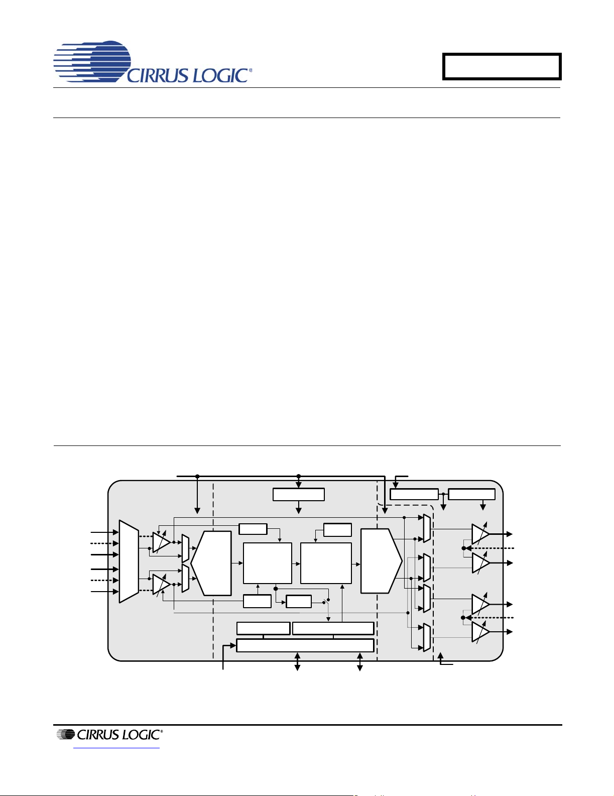
GENERAL DESCRIPTION
The CS42L55 is a highly integrated, 24-bit, ultra-low
power stereo CODEC based on multi-bit delta-sigma
modulation. Both the ADC and DAC offer many features
suitable for low power portable system applications.
The analog input path allows independent channel
control of a variety of features. The Programmable Gain
Amplifier (PGA) provides analog gain with zero cross
transitions. The ADC path includes a digital volume attenuator with soft ramp transitions and a p rogrammable
ALC and noise gate monitor the input signals and adjust
the volume appropriately. An analog passthrough also
exists, accommodating a lower noise, lower power analog in to analog out path to the headphone and line
amplifiers, bypassing the ADC and DAC.
The DAC output path includes a fixed-function digital
signal processing engine. Tone control provides bass
and treble adjustment at four selectable corner freque ncies. The digital mixer provides independent volume
control for both the ADC output and PCM input signal
paths, as well as a master volume control. Digital volume controls may be configured to change on soft ramp
transitions while the analog controls can be configured
to occur on every zero crossing. The DAC path also includes de-emphasis, limiting functions and a beep
generator delivering tones selectable across a range of
two full octaves.
The Class H stereo headphone amplifier combines the
efficiency of an integrated step-down and inverting
charge pump with the linearity and low EMI of a Class
AB amplifier. A step-down/inverting charge pump operates in two modes: +/-VCP mode or +/-(VCP/2) mode.
Based on the amplifier’s output signal, internal logic automatically adjusts the output of the charge pump,
+VHPFILT and –VHPFILT, to optimize efficiency. With
these features, the amplifier delivers a ground-centered
output with a large signal swing even at low voltages
and eliminates the need for external DC-blocking
capacitors.
These features make the CS42L55 the ideal solution for
portable applications that require extremely low power
consumption in a minimal amount of space.
The CS42L55 is available in a 36-pin QFN package for
the Commercial (-40°C to +85°C) grade. The
CDB42L55 Customer Demonstration board is also
available for device evaluation and implementation suggestions. Please see “Ordering Information” on page 73
for complete details.
2 DS773F1
Page 3

TABLE OF CONTENTS
1. PIN DESCRIPTIONS .............................................................................................................................. 8
1.1 I/O Pin Characteristics .......................... ... .... ... ... ... .... ... ... ... .... ... ... ..................................................... 9
2. TYPICAL CONNECTION DIAGRAM ................................................................................................... 10
3. CHARACTERISTIC AND SPECIFICATION TABLES ......................................................................... 11
RECOMMENDED OPERATING CONDITIONS ................................................................................... 11
ABSOLUTE MAXIMUM RATINGS .......................................................................................................11
ANALOG INPUT CHARACTERISTICS ................................................................................................ 12
ADC DIGITAL FILTER CHARACTERISTICS ....................................... ... .... ... ... ... ................................ 13
HP OUTPUT CHARACTERISTICS ......................................................................................................14
LINE OUTPUT CHARACTERISTICS ................................................................................................... 15
ANALOG PASSTHROUGH CHARACTERISTICS ............................................................................... 16
COMBINED DAC INTERPOLATION & ON-CHIP ANALOG FILTER RESPONSE .............................. 16
SWITCHING SPECIFICATIONS - SERIAL PORT ............................................................................... 17
SWITCHING SPECIFICATIONS - CONTROL PORT .......................................................................... 18
POWER SUPPLY REJECTION (PSRR) CHARACTERISTICS ........................................................... 19
DIGITAL INTERFACE SPECIFICATIONS & CHARACTERISTICS ..................................................... 19
POWER CONSUMPTION - ALL SUPPLIES = 1.8 V ............................................................................ 20
POWER CONSUMPTION - ALL SUPPLIES = 2.5 V ............................................................................ 21
4. APPLICATIONS ................................................................................................................................... 22
4.1 Overview ......................................................................................................................................... 22
4.1.1 Basic Architecture ................................................................................................................. 22
4.1.2 Line Inputs ............................................................................................................................. 22
4.1.3 Line and Headphone Outputs (Class H, Ground-Centered Amplifiers) ................................. 22
4.1.4 Fixed-Function DSP Engine .................................................................................................. 22
4.1.5 Beep Generator ..................................................................................................................... 22
4.1.6 Power Management .............................................................................................................. 22
4.2 Analog Inputs ................................................................................................................................. 23
4.2.1 Pseudo-Differential Inputs ........................... ................................................................. .........24
4.2.2 Automatic Level Control (ALC) .............................................................................................. 24
4.3 Analog In to Analog Out Passthrough ............................................................................................ 25
4.4 Analog Outputs .............................................................................................................................. 26
4.5 Class H Amplifier ............................................................................................................................ 27
4.5.1 Power Control Options ................... .... ... ... ... .... ... ... ... .... ... ...................................................... 27
4.5.1.1 Standard Class AB Operation (Mode 01 and 10) ...................................................... 28
4.5.1.2 Adapted to Volume Settings (Mode 00) .................................. ... .... ... ... ... ... ................ 28
4.5.1.3 Adapted to Output Signal (Mode 11) ......................................................................... 29
4.5.2 Power Supply Transitions ...................................................................................................... 29
4.5.3 Efficiency ............................................................................................................................... 31
4.6 Beep Generator .............................................................................................................................. 31
4.7 Limiter ............................................................................................................................................. 32
4.8 Serial Port Clocking ........................................................................................................................ 34
4.9 Digital Interface Format .................................................................................................................. 34
4.10 Initialization ............................ .... ... ... ... ... ....................................... ... .... ... ... ... ................................ 34
4.11 Recommended DAC to HP or Line Power-Up Sequence (Playback) .... ... ... .... ... ... ... ... .... ... ... ... ... 35
4.11.1 Recommended Power-Down Sequence ............................................................................. 36
4.12 Recommended PGA to HP or Line Power-Up Sequence (Analog Passthrough) ................ ......... 36
4.12.1 Recommended Power-Down Sequence ............................................................................. 36
4.13 Required Initialization Settings ..................................................................................................... 37
4.14 Control Port Operation .................................................................................................................. 38
4.14.1 I²C Control .............. ... ... .... ... ... ....................................... ... ... ... .... ... ... ... .... ... ... ...................... 38
4.14.2 Memory Address Pointer (MAP) .................................... ... ... ... .... ... ... ... .... ... ... ... ... .... ... ... ... ... 39
4.14.2.1 Map Increment (INCR) ............................................................................................. 39
CS42L55
DS773F1 3
Page 4

CS42L55
5. REGISTER QUICK REFERENCE ........................................................................................................ 40
6. REGISTER DESCRIPTION .................................................................................................................. 42
6.1 Fab I.D. and Revision Register (Address 01h) (Read Only) ........................................................... 42
6.1.1 Chip Revision (Read Only) .................................................................................................... 42
6.2 Power Control 1 (Address 02h) ...................................................................................................... 42
6.2.1 Power Down ADC Charge Pump .......................................................................................... 42
6.2.2 Power Down ADC x ............................................................................................................... 42
6.2.3 Power Down ...... .... ... ....................................... ... ... ....................................... ... ... ... ................ 42
6.3 Power Control 2 (Address 03h) ...................................................................................................... 43
6.3.1 Headphone Power Control .... ... ... ... .... ... ....................................... ... ... ... .... ... ... ... ... .... ... ......... 43
6.3.2 Line Power Control ... ... ... ....................................... ... .... ... ... ... ... .... ... ... ... ................................ 43
6.4 Clocking Control 1 (Address 04h) ................................................................................................... 43
6.4.1 Master/Slave Mode .................................. ............................................................................. 43
6.4.2 SCLK Polarity ........ ... ... ....................................... ... ... ....................................... ... ... ................ 43
6.4.3 SCLK Equals MCLK ........................................ ... ... ... ....................................... ... ... .... ............ 44
6.4.4 MCLK Divide By 2 .......... ....................................... ... .... ... ...................................... .... ............ 44
6.4.5 MCLK Disable .......................... ....................................... ... ....................................... ............ 44
6.5 Clocking Control 2 (Address 05h) ................................................................................................... 44
6.5.1 Speed Mode ...... .... ... ....................................... ... ... ....................................... ... ... ... ................ 44
6.5.2 32 kHz Sample Rate Group ..................................................................................................45
6.5.3 Internal MCLK/LRCK Ratio ................................................................................................... 45
6.6 Class H Power Control (Address 06h) ............................................................................................ 45
6.6.1 Adaptive Power Adjustment ............... ... ... ... .... ... ... ... .... ...................................... ... .... ... ... ... ... 45
6.7 Miscellaneous Control (Address 07h) ............................................................................................. 45
6.7.1 Digital MUX ........................ ...................................... ....................................... ... ................... 45
6.7.2 Analog Zero Cross ............................. ... ... ... .... ...................................... .... ... ... ...................... 46
6.7.3 Digital Soft Ramp ........................ ... .... ...................................... ............................................. 46
6.7.4 Freeze Registers ...... ... ... .... ...................................... .... ... ... ... ... .... ......................................... 46
6.8 ADC, Line, HP MUX (Address 08h) ................................................................................................ 46
6.8.1 ADC x Input Select ... ... ... .... ...................................... .... ... ... ....................................... ............ 46
6.8.2 Line Input Select ............................. .... ... ....................................... ... ... ... ................................ 47
6.8.3 Headphone Input Select ........................................................................................................ 47
6.9 HPF Control (Address 09h) ............................................................................................................ 47
6.9.1 ADCx High-Pass Filter .......................................................................................................... 47
6.9.2 ADCx High-Pass Filter Freeze .............................................................................................. 47
6.9.3 HPF x Corner Frequency ................................ ... ... ... .... ... ... ... ... .... ... ... ................................... 47
6.10 Misc. ADC Control (Address 0Ah) ................................................................................................ 48
6.10.1 ADC Channel B=A .............................................................................................................. 48
6.10.2 PGA Channel B=A .............................................................................................................. 48
6.10.3 Digital Sum .......................................................................................................................... 48
6.10.4 Invert ADC Signal Polarity ................................................................................................... 48
6.10.5 ADC Mute ............................................................................................................................ 48
6.11 PGA x MUX, Volume:
PGA A (Address 0Bh) & PGA B (Address 0Ch) ................................................................................... 49
6.11.1 Boostx ................................................................................................................................. 49
6.11.2 PGA x Input Select .............................................................................................................. 49
6.11.3 PGAx Volume ...................................................................................................................... 49
6.12 ADCx Attenuator Control:
ADCAATT (Address 0Dh) & ADCBATT (Address 0Eh) ....................................................................... 50
6.12.1 ADCx Volume ...................................................................................................................... 50
6.13 Playback Control 1 (Address 0Fh) .........................................................................................
6.13.1 Power Down DSP ................................................................................................................ 50
6.13.2 HP/Line De-Emphasis ......................................................................................................... 50
6.13.3 Playback Channels B=A ...................................................................................................... 50
....... 50
4 DS773F1
Page 5

CS42L55
6.13.4 Invert PCM Signal Polarity .................................................................................................. 51
6.13.5 Master Playback Mute ......................................................................................................... 51
6.14 ADCx Mixer Volume:
ADCA (Address 10h) & ADCB (Address 11h) ...................................................................................... 51
6.14.1 ADC Mixer Channel x Mute ................................................................................................. 51
6.14.2 ADC Mixer Channel x Volume ............................................................................................. 51
6.15 PCMx Mixer Volume:
PCMA (Address 12h) & PCMB (Address 13h) ..................................................................................... 52
6.15.1 PCM Mixer Channel x Mute ................................................................................................52
6.15.2 PCM Mixer Channel x Volume ............................................................................................ 52
6.16 Beep Frequency & On Time (Address 14h) ................................................................................. 53
6.16.1 Beep Frequency ........... .... ... ... ....................................... ... ... ... .... ... ... ... .... ... ... ...................... 53
6.16.2 Beep On Time ..................... ... ... ... .... ... ... ... .... ... ... ... .... ...................................... ... .... ............ 54
6.17 Beep Volume & Off Time (Address 15h) ......................................................................................54
6.17.1 Beep Off Time ..................... ... ... ... .... ... ... ... .... ...................................... .... ... ... ... ... .... ............ 54
6.17.2 Beep Volume .......... ... ... .... ... ....................................... ... ... ... ... .... ... ... ... .... ... ... ... ... .... ............ 55
6.18 Beep & Tone Configuration (Address 16h) ...................................................................................55
6.18.1 Beep Configuration ........................................... ... ... .... ... ... ... ................................................ 55
6.18.2 Treble Corner Frequency ................. ... ... ... .... ... ... ... .... ... ... ... ... .... ... ... ... .... ... ... ... ................... 55
6.18.3 Bass Corner Frequency ............................ .... ... ... ... .... ... ... ... ... ....................................... ...... 56
6.18.4 Tone Control Enable ........................................................................ ... .... ... ... ... ... .... ... ......... 56
6.19 Tone Control (Address 17h) ............ ... ... .... ... ... ... .... ... ... ....................................... ... ... ... .... ............ 56
6.19.1 Treble Gain .......................................................................... ... .... ... ... ... .... ... ... ... ... ................ 56
6.19.2 Bass Gain ..................................... .... ... ... ....................................... ... ... ................................ 56
6.20 Master Volume Control:
MSTA (Address 18h) & MSTB (Address 19h) ...................................................................................... 57
6.20.1 Master Volume Control ........................................................................................................ 57
6.21 Headphone Volume Control:
HPA (Address 1Ah) & HPB (Address 1Bh) ..........................................................................................57
6.21.1 Headphone Channel x Mute ................................................................................................57
6.21.2 Headphone Volume Control ................................................................................................57
6.22 Line Volume Control:
LINEA (Address 1Ch) & LINEB (Address 1Dh) .................................................................................... 58
6.22.1 Line Channel x Mute ........................................... ... .... ... ... ................................................... 58
6.22.2 Line Volume Control ............................................................................................................ 58
6.23 Analog Input Advisory Volume (Address 1Eh) ............................................................................. 59
6.23.1 Analog Input Advisory Volume ............... ... .... ... ... ... .... ... ... ... ... .... ... ......................................59
6.24 Digital Input Advisory Volume (Address 1Fh) ............ ............................................. ......................59
6.24.1 Digital Input Advisory Volume ............................................................................................. 59
6.25 ADC & PCM Channel Mixer (Address 20h) .................................................................................. 60
6.25.1 PCM Mix Channel Swap ........................................ .... ... ... ... ... .... ......................................... 60
6.25.2 ADC Mix Channel Swap ...................................... ... .... ... ... ... ... .... ... ... ... ................................ 60
6.26 Limiter Min/Max Thresholds (Address 21h) ..................................................................................60
6.26.1 Limiter Maximum Threshold ......... .... ... ... ... .... ... ... ... .... ... ... ... ... .... ... ... ... .... ... ... ... ... .... ... ... ... ... 60
6.26.2 Limiter Cushion Threshold .................................................................................................. 61
6.27 Limiter Control, Release Rate (Address 22h) ...............................................................................61
6.27.1 Peak Detect and Limiter ............ ... .... ... ... ... .... ... ... ....................................... ... ... ... .... ... ......... 61
6.27.2 Peak Signal Limit All Channels ........................................................................................... 61
6.27.3 Limiter Release Rate ........ ... ... ... ... ....................................... ... .... ... ... ... .... ... ... ... ... .... ... ......... 62
6.28 Limiter Attack Rate (Address 23h) ................................................................................................ 62
6.28.1 Limiter Attack Rate ....... .... ... ... ... ... .... ... ....................................... ... ... ... .... ... ... ... ... .... ..
6.29 ALC Enable & Attack Rate (Address 24h) ....................................................................................62
6.29.1 ALCx ............................. .... ... ... ... ... .... ... ... ....................................... ... ... .... ............................ 62
6.29.2 ALC Attack Rate .................................................................................................................. 63
.......... 62
DS773F1 5
Page 6

CS42L55
6.30 ALC Release Rate (Address 25h) ................................................................................................ 63
6.30.1 ALC Release Rate ............................................................................................................... 63
6.31 ALC Threshold (Address 26h) ...................................................................................................... 64
6.31.1 ALC Maximum Threshold .................................................................................................... 64
6.31.2 ALC Minimum Threshold ..................................................................................................... 64
6.32 Noise Gate Control (Address 27h) ............................................................................................... 64
6.32.1 Noise Gate All Channels ..................................................................................................... 64
6.32.2 Noise Gate Enable .............................................................................................................. 65
6.32.3 Noise Gate Threshold and Boost ........................................................................................ 65
6.32.4 Noise Gate Delay Timing .................................................................................................... 65
6.33 ALC and Limiter Soft Ramp, Zero Cross Disables (Address 28h) ................................................ 65
6.33.1 ALCx Soft Ramp Disable ..................... ... ....... ...... ....... ...... ...... ....... ...... ....... ...... ....... ...... ...... 65
6.33.2 ALCx Zero Cross Disable .................................................................................................... 65
6.33.3 Limiter Soft Ramp Disable ......................... ....... ...... ....... ...... ....... ...... ....... ...... ...... ....... ......... 66
6.34 Status (Address 29h) (Read Only) ............................................................................................... 66
6.34.1 HPDETECT Pin Status (Read Only) .......................................... ... ... ... .... ... ... ... ... .... ... ... ... ... 66
6.34.2 Serial Port Clock Error (Read Only) .................................................................................... 66
6.34.3 DSP Engine Overflow (Read Only) ..................................................................................... 66
6.34.4 MIXx Overflow (Read Only) ................................................................................................. 66
6.34.5 ADCx Overflow (Read Only) ...............................................................................................67
6.35 Charge Pump Frequency (Address 2Ah) ..................................................................................... 67
6.35.1 Charge Pump Frequency .................................................................................................... 67
7. PCB LAYOUT CONSIDERATIONS ..................................................................................................... 68
7.1 Power Supply ................................................................................................................................. 68
7.2 Grounding ....................................................................................................................................... 68
7.3 QFN Thermal Pad .......................................................................................................................... 68
8. ANALOG VOLUME NON-LINEARITY (DNL & INL) ............... .... ... ... ... ... .... ... ... ... .... ... ... ... ... .... ... ... ... ... 69
9. ADC & DAC DIGITAL FILTERS .......................................................................................................... 70
10. PARAMETER DEFINITIONS .............................................................................................................. 71
11. PACKAGE DIMENSIONS .................................................................................................................. 72
THERMAL CHARACTERISTICS .......................................................................................................... 72
12. ORDERING INFORMATION .............................................................................................................. 73
13. REFERENCES .................................................................................................................................... 73
14. REVISION HISTORY .......................................................................................................................... 73
LIST OF FIGURES
Figure 1.Typical Connection Diagram ....................................................................................................... 10
Figure 2.CMRR Test Configuration ................................. .......................................................................... 12
Figure 3.HP Output Test Configuration ............................... ... ... ... .... ... ... ... ... .... ... ... ... .... ... ......................... 15
Figure 4.Line Output Test Configuration .......................................... ... ... ... ... .... ... ...................................... 15
Figure 5.Serial Port Timing (Slave Mode) ....... ... .... ... ... ... .... ... ... ... .... ... ... ... ... ............................................. 17
Figure 6.Serial Port Timing (Master Mode) .. ............................................................................................. 17
Figure 7.I²C Control Port Timing ............................................................................................................... 18
Figure 8.Power Consumption Test Configuration ..................................................................................... 19
Figure 9.Analog Input Signal Flow ............................................................................................................ 23
Figure 10.Stereo Pseudo-Differential Input ............................................................................................... 24
Figure 11.ALC Operation .......... ... ... ... .... ... ... ... ... .... ... ....................................... ... ... ... .... ... ... ...................... 25
Figure 12.DSP Engine Signal Flow ........................................................................................................... 26
Figure 13.Analog Output Stage ................................................................................................................. 27
Figure 14.Adaptive Mode 00 ..... ... ... ... .... ... ... ....................................... ... ... ... .... ... ... ... .... ... ... ...................... 28
Figure 15.VHPFILT Transitions ................................................................................................................. 30
Figure 16.VHPFILT Hysteresis .......... .... ... ... ... ... .... ... ....................................... ... ... ... .... ... ......................... 30
Figure 17.Class H Power to Load vs. Power from VCP Supply ................................................................ 31
6 DS773F1
Page 7

CS42L55
Figure 18.Beep Configuration Options ...................................................................................................... 32
Figure 19.Peak Detect & Limiter ............................................................................................................... 33
Figure 20.I²S Format ................................................................................................................................. 34
Figure 21.Control Port Timing, I²C Write ................................................................................................... 38
Figure 22.Control Port Timing, I²C Read ................................................................................................... 38
Figure 23.PGA Step Size vs. Volume Setting ........................................................................................... 69
Figure 24.PGA Output Volume vs. Volume Setting .................................................................................. 69
Figure 25.HP/Line Step Size vs. Volume Setting ...................................................................................... 69
Figure 26.HP/Line Output Volume vs. Volume Setting .............................................................................69
Figure 27.ADC Passband Ripple ........... ... ................................................................................................ 70
Figure 28.ADC Stopband Rejection .......................................................................................................... 70
Figure 29.ADC Transition Band ................................................................................................................ 70
Figure 30.ADC Transition Band Detail ...................................................................................................... 70
Figure 31.DAC Passband Ripple ........... ... ... ... ... .... ...................................... .... ... ... ... .... ... ... ... ... ................ 70
Figure 32.DAC Stopband .......................................................................................................................... 70
Figure 33.DAC Transition Band ................................................................................................................ 70
Figure 34.DAC Transition Band (Detail) .................................................................................................... 70
DS773F1 7
Page 8
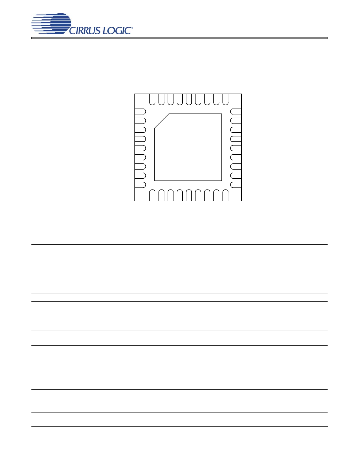
1. PIN DESCRIPTIONS
CS42L55
SDIN
LRCK
SDA
SCL
VCP
FLYP
+VHPFILT
FLYC
FLYN
MCLK
SCLK
1
2
3
4
5
6
7
8
9
10 11 12 13 14 15 181716
SDOUT
35 28
333436
GND/Thermal Pad
Top-Down (Through Package)
VL
32
View
VLDO
VDFILT
HPDETECT
RESET
293031
AIN1B
27
26
25
24
23
22
21
20
19
AIN1REF
AIN1A
AIN2B
AIN2REF
AIN2A
AFILTB
AFILTA
VQ
FILT+
VA
HPREF
HPOUTA
-VHPFILT
HPOUTB
LINEOUTA
LINEREF
LINEOUTB
AGND
Pin Name # Pin Description
SDIN 1 Serial Audio Data Input (Input) - Input for two’s complement serial audio data.
LRCK 2
SDA 3 Serial Control Data (Input/Output) - Serial data for the I²C serial control port.
SCL 4 Serial Control Port Clock (Input) - Serial clock for the I²C serial control port.
VCP 5 Step-Down Charge Pump Power (Input) - Power supply for the step-d own charge pump.
FLYP 6
+VHPFILT 7
FLYC 8
FLYN 9
-VHPFIL T 10
HPOUTA
HPOUTB
HPREF 12 Pseudo Diff. Hea dphone Output Reference (Input) - Ground reference for the headphone amplifiers
LINEOUTA
LINEOUTB
LINEREF 15 Pseudo Diff. Line Output Reference (Input) - Ground reference for the line amplifiers.
Left Right Clock (Input/Output) - Determines which channel, Left or Right, is currently active on the
serial audio data lines.
Charge Pump Cap Positive Node (Output) - Positive node for the step-down charge pump’s flying
capacitor.
Step-Down Charge Pump Filter Connection (Output) - Power supply from the step-down charge
pump that provides the positive rail for the headphone and line amplifiers
Charge Pump Cap Common Node (Output) - Common positive node for the step-down and inverting
charge pumps’ flying capacitors.
Charge Pump Cap Negative Node (Output) - Negative node for the inverting charge pump’s flying
capacitor.
Inverting Charge Pump Filter Connection (Output) - Power supply from the inverting charge pump
that provides the negative rail for the headphone and line amplifiers.
1113Headphone Audio Ou tput (Output) - The full-scale output level is specified in the HP Output Charac-
teristics specification table
1416Line Audio Output (Output) - The full-scale output level is specified in the Line Output Characteristics
specification table
8 DS773F1
Page 9
CS42L55
VA 17 Analog Power (Input) - Power supply for the internal analog section.
AGND 18 Analog Ground (Input) - Ground reference for the internal analog section.
FILT+ 19 Positive Voltage Reference (Output) - Positive reference voltage for the internal sampling circuits.
VQ 20 Quiescent Voltage (Output) - Filter connection for the internal quiescent voltage.
AFILTA
AFILTB
AIN2A
AIN2B
AIN1A
AIN1B
AIN2REF
AIN1REF
HPDETECT 29
21
Antialias Filter Connection (Output) - Antialias filter connection for the ADC inputs.
22
23
25
Analog Input (Input) - The full-scale level is specified in the Analog Input Characteristics specification
26
table.
28
2427Pseudo Diff. Analog Input Reference (Input) - Ground reference for the programmable gain amplifi-
ers (PGA).
Headphone Detect (Input) - Powers down the left and/or right channel of the line and/or headphone
outputs as described in “Headphone Power Control” on page 43 and “Line Power Control” on page 43.
RESET
VLDO 31 Low Dropout Regulator (LDO) Power (Input) - Power supply for the LDO regulator.
VDFILT 32
VL 33
SDOUT 34 Serial Audio Data Output (Output) - Output for two’s complement serial audio data.
MCLK 35 Master Clock (Input) - Clock source for the delta-sigma modulators.
SCLK 36 Serial Clock (Input/Output) - Serial clock for the serial audio interface.
GND/
Thermal Pad
30 Reset (Input) - The device enters a low power mode when this pin is driven low.
Low Dropout Regulator (LDO) Filter Connectio n (Output) - Power supply from the LDO regulator
that provides the low voltage power to the digital section.
Digital Interface Power (Input) - Determines the required signal level for the serial audio inte rface
and I²C control port.
Ground reference for the internal charge pump and digital section; thermal relief pad. See “QFN Ther-
-
mal Pad” on page 68 for more information.
1.1 I/O Pin Characteristics
Input and output levels and associated power supply voltage are shown in the table below. Logic levels
should not exceed the corresponding power supply voltage.
Power
Supply
VL
VA HPDETECT Input - - 1.8 V - 2.5 V, with Hysteresis
Pin Name I/O Internal
Connections
RESET
SCL Input - - 1.8 V - 3.3 V, with Hysteresis
SDA Input/Output - CMOS/Open Drain 1.8 V - 3.3 V, with Hysteresis
MCLK Input - - 1.8 V - 3.3 V
LRCK Input/Output
SCLK Input/Output
SDOUT Output - 1.8 V - 3.3 V, CMOS 1.8 V - 3.3 V
SDIN Input - - 1.8 V - 3.3 V
Input - - 1.8 V - 3.3 V, with Hysteresis
Weak Pull-up
(~1 MΩ)
Weak Pull-up
(~1 MΩ)
Driver Receiver
1.8 V - 3.3 V, CMOS 1.8 V - 3.3 V
1.8 V - 3.3 V, CMOS 1.8 V - 3.3 V
DS773F1 9
Page 10
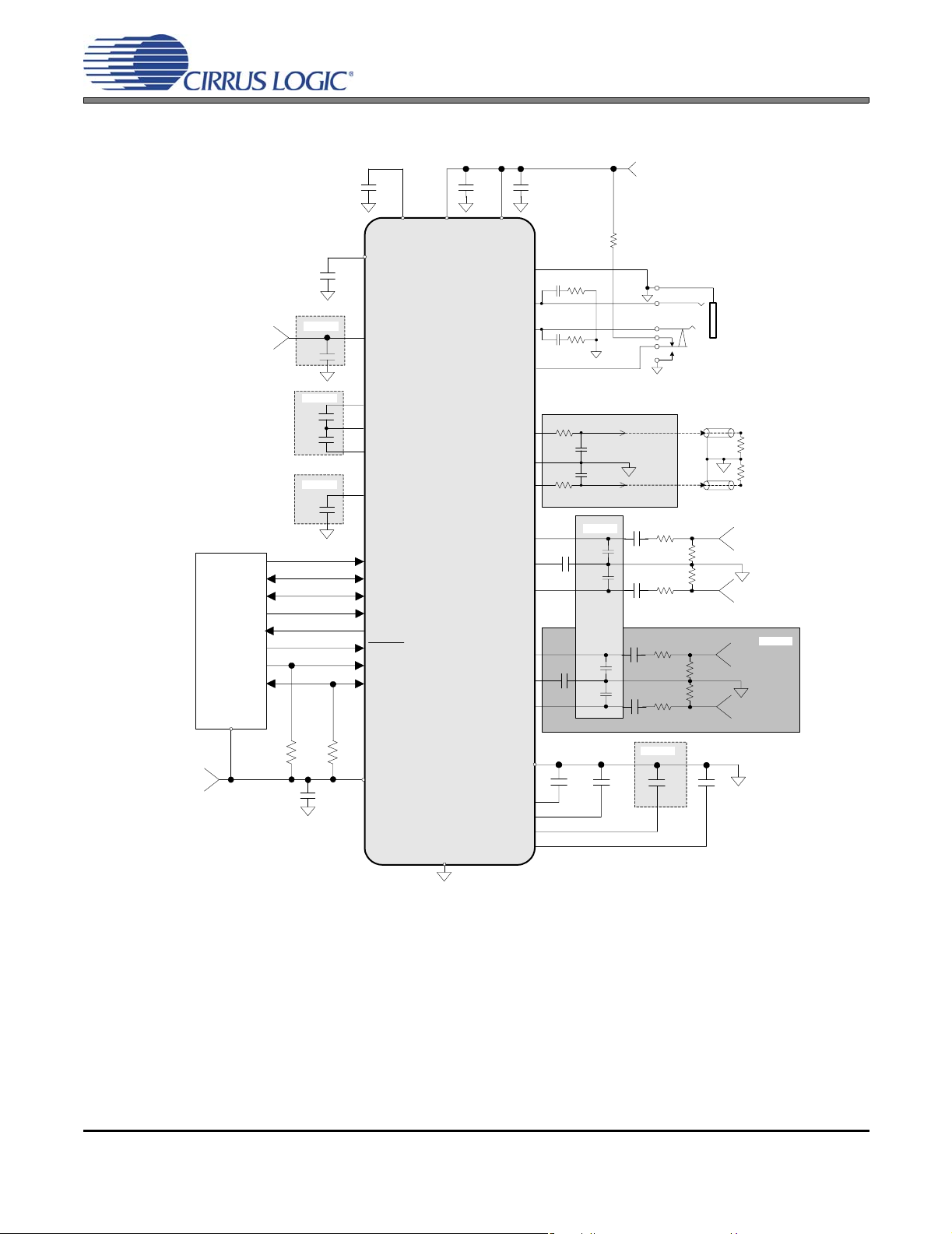
2. TYPICAL CONNECTION DIAGRAM
1 µF
** **
0.1 µF
CS42L55
0.1 µF
**
+1.65 V to +2.71 V
VA
HPREF
HPOUTB
HPOUTA
0.1 µF
**
**
0.1 µF
47 kΩ
33 Ω
33 Ω
+1.65 V to +2.71 V
2.2 µF
2.2 µF
Note 1
**
**
VDFILT
+VHPFILT
VCP
VLDO
HPDETECT
CS42L55
LINEOUTA
LINEREF
LINEOUTB
AIN1A
AIN1REF
AIN1B
AIN2A
AIN2REF
AIN2B
562 Ω
562 Ω
1 µF
1 µF
3300 pF
*
*
3300 pF
Note 4
1800 pF
**
1800 pF
1800 pF
**
1800 pF
Digital Audio
Processor
2 kΩ
Note 2
2.2 µF
2.2 µF
Note 1
2.2 µF
2 k
FLYP
**
FLYC
**
FLYN
-VHPFILT
**
MCLK
SCLK
LRCK
SDIN
SDOUT
RESET
SCL
SDA
Ω
AGND
+1.65 V to +3.47 V
0.1 µF
VL
**
AFILTA
*
1000 pF
1000 pF
AFILTB
VQ
GND/Thermal Pad
Notes:
1. The headphone amplifier’s output power and distortion are rated using the nominal capacitance shown. Larger capacitance
reduces the ripple on the internal amplifiers’ supplies and in turn reduces the amplifier’s distortion at high output power levels.
Smaller capacitance may not sufficiently reduce ripple to achieve the rated output power and distortion. Since the actual value
of typical X7R/X5R ceramic capacitors deviates from the nominal value by a percentage specified in the manufacturer’s data
sheet, capacitors should be selected based on the minimum output power and maximum distortion required.
2. The headphone amplifier’s output power and distortion are rated using the nominal capacitance shown and using the default
charge pump switching frequency. The required capacitance follows an inverse relationship with the charge pump’s switching
frequency. When increasing the switching frequency, the capacitance may decrease; when lowering the switching frequency,
the capacitance must increase. Since the actual value of typical X7R/X5R ceramic capacitors deviates from the nominal value
by a percentage specified in the manufacturer’s data sheet, capacitors should be selected based on the minimum output
power, maximum distortion and maximum charge pump switching frequency required.
3. Additional bulk capacitance may be added to improve PSRR at low frequencies.
4. These capacitors serve as a charge reservoir for the internal switched capacitor ADC modulators and should be placed as
close as possible to the inputs. They are only needed when the PGA (Programmable Gain Amplifier) is bypassed.
5. Input pairs (such as AIN2A, AIN2REF and AIN2B) may be left floating if they are not used.
FILT+
Headphone Out
Left & Right
LPF is Optional
**
*
1 µF
*
**
1 µF
**
*
1 µF
*
**
1 µF
Note 3
*
*
NPO/C0G dielectric capacitors.
**
Low ESR, X7R/X5R dielectric capacitors.
100 Ω
100 Ω
100 Ω
100 Ω
**
2.2 µF
100 kΩ
100 kΩ
100 kΩ
100 kΩ
R
R
**
2.2 µF
ext
Line Level Out
Left & Right
ext
Analog
Input 1
Note 5
Analog
Input 2
Figure 1. Typical Connection Diagram
10 DS773F1
Page 11
3. CHARACTERISTIC AND SPECIFICATION TABLES RECOMMENDED OPERATING CONDITIONS
GND = AGND = 0 V, all voltages with respect to ground.
Parameters Symbol Min Max Units
DC Power Supply
Analog
Charge Pump
LDO Regulator for Digital
Serial/Control Port Interface
Ambient Temperature Commercial - CNZ
VA 1.65 2.71 V
VCP 1.65 VA V
VLDO 1.65 2.71 V
VL 1.65 3.47 V
T
A
ABSOLUTE MAXIMUM RATINGS
GND = AGND = 0 V; all voltages with respect to ground.
Parameters Symbol Min Max Units
DC Power Supply Analog, Charge Pump, LDO
Serial/Control Port Interface
Input Current (Note 2)
Analog Input Voltage (Note 3) V
Digital Input Voltage (Note 3)
VA, VCP, VLDOVL-0.3
I
in
IN
V
IND
CS42L55
-40 +85 °C
3.0
-0.3
-±10mA
AGND-0.7 VA+0.7
-0.3 VL+0.4 V
4.0
V
V
V
Ambient Operating Temperature (power applied)
Storage Temperature
T
A
T
stg
-50 +115 °C
-65 +150 °C
WARNING:Operation at or beyond these limit s may result in permanent damage to the device. Normal operation
is not guaranteed at these extremes.
Notes:
1. Due to the existence of parasitic body diodes between VCP and VA, cu rrent flows from VCP to V A whenever the VA power supply is lower than VCP. This causes a “back-powering” effect on the VA power
supply rails internal to the part. Hence VA should be maintained at an equal or greater voltage than VCP
at all times. While “back-powering” does not have any adverse effects on device operation with respect
to performance and reliability , it does lead to extra power consumption and therefore should be avoided.
2. Any pin except supplies. Transient currents of up to ±100 mA on the analog input pins will not cause
SCR latch-up.
3. The maximum over/under voltage is limited by the input current.
DS773F1 11
Page 12
CS42L55
ANALOG INPUT CHARACTERISTICS
Test Conditions (unless otherwise specified): Connections to the CS42L55 are shown in the Figure 1. "Typical Connection Dia-
gram" on page 10; Input is a 1 kHz sine wave through the passive input filter, PGA = 0 dB; All Supplies = VA;
GND = AGND = 0 V; TA=+25°C; Measurement bandwidth is 20 Hz to 20 kHz. Sample Frequency = 48 kHz.
VA = 2.5 V VA = 1.8 V
Parameter
Analog In to ADC (PGA bypassed)
Dynamic Range A-weighted
Total Harmonic Distortion + Noise -1 dBFS
Analog In to PGA to ADC
Dynamic Range
PGA Setting: 0 dB A-weighted
PGA Setting: +12 dB A-weighted
Total Harmonic Distortion + Noise
PGA Setting: 0 dB -1 dBFS
-60 dBFS
PGA Setting: +12 dB -1 dBFS
Common Mode Rejection (Note 5)
DC Accuracy
Interchannel Gain Mismatch
Gain Drift
Offset Error (Note 6)
Input
Interchannel Isolation (1 kHz)
HP Amp to Analog Input Isolation R
Full-scale Input Voltage ADC
Input Impedance (Note 7) ADC
(Note 4)
unweighted
-20 dBFS
-60 dBFS
unweighted
unweighted
= 10 kΩ
L
RL = 16 Ω
PGA (0 dB)
PGA (+12 dB)
PGA
Min Typ Max Min Typ Max Unit
89
86
-
-
-
88
85
81
78
-
-
- -83 -77 - -81 -75 dB
-40--40-dB
- 0.2 - - 0.2 - dB
- ±100 - - ±100 - ppm/°C
- 352 - - 352 - LSB
-90--90-dB
-
-
0.76•VA
0.78•VA
-
-
95
92
-85
-72
-32
94
91
87
84
-87
-31
90
83
0.80•VA
0.82•VA
0.198•VA
60
40
-
-
-79
-
-26
-
-
-
-
-81
-25
-
-
0.84•VA
0.86•VA
-
-
86
83
-
-
-
85
82
78
75
-
-
-
-
0.76•VA
0.78•VA
-
-
92
89
-85
-69
-29
91
88
84
81
-85
-28
90
83
0.80•VA
0.82•VA
0.198•VA
60
40
-
-
-79
-
-23
-
-
-
-
-79
-22
-
-
0.84•VA
0.86•VA
-
-
dB
dB
dB
dB
dB
dB
dB
dB
dB
dB
dB
dB
dB
Vpp
Vpp
Vpp
kΩ
kΩ
4. Referred to the typical full-scale voltage. Applies to all THD+N and Dynamic Range values in the table.
5. See test figure shown below.
6.
SDOUT Code with HPFx=1;HPFRZx=0.
7. Measured between AINxx and AGND.
100 mVPP,
25 Hz
100 Ω
1 μF
AINxA
AINxREF
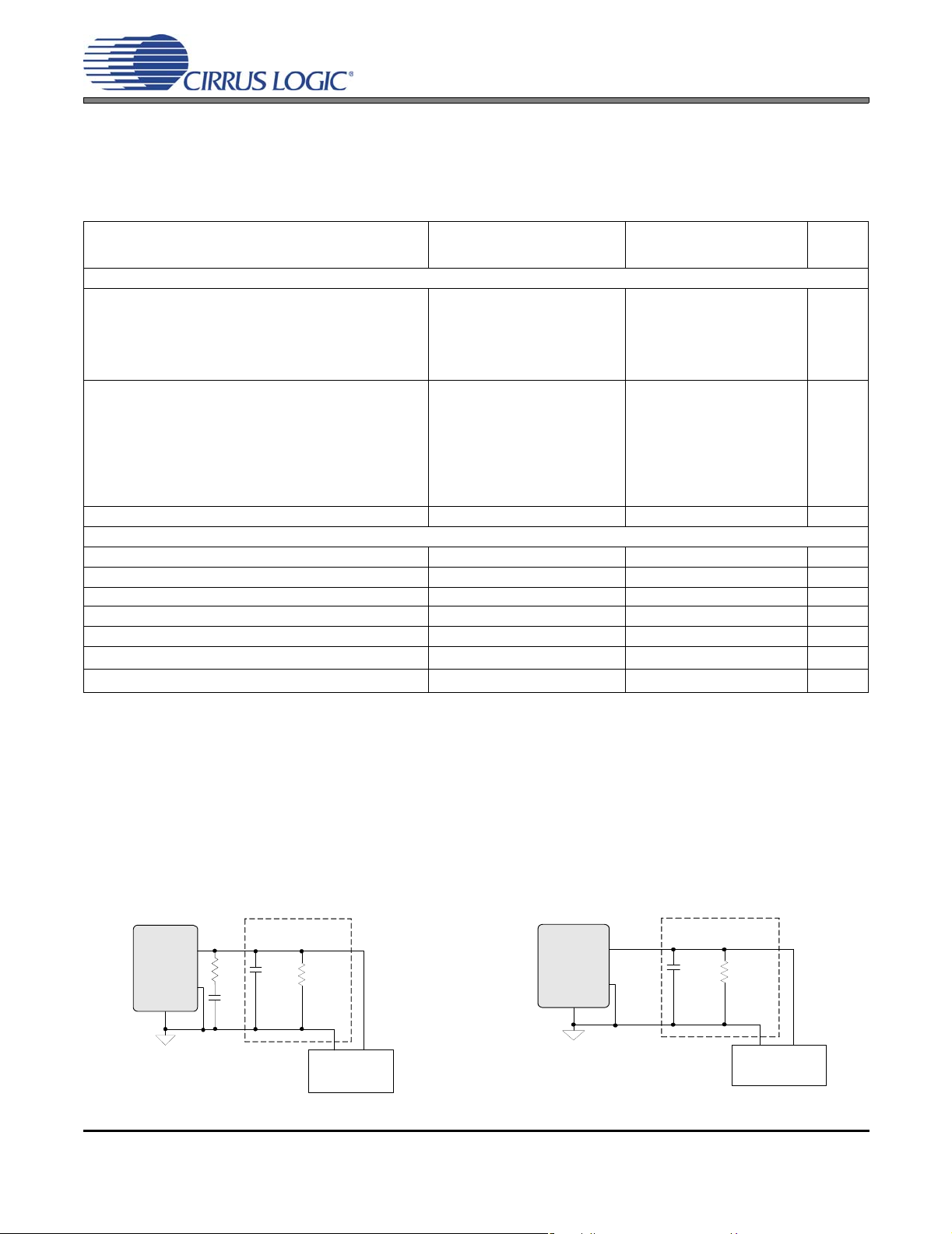
Figure 2. CMRR Test Configuration
12 DS773F1
Page 13
ADC DIGITAL FILTER CHARACTERISTICS
Parameter (Note 8) Min Typ Max Unit
Frequency Response (20 Hz to 20 kHz)
Passband to -0.05 dB corner
to -3 dB corner
Stopband
Stopband Attenuation
Total Group Delay
High-Pass Filter Characteristics (48 kHz Fs) (Note 9)
Passband to -3.0 dB corner
to -0.05 dB corner
Passband Ripple
Phase Deviation @ 20 Hz
Filter Settling Time (Note 10)
Notes:
8. Response is clock-dependent and will scale with Fs. Note that the response plots (Figures 27 to 30 on
page 70) have been normalized to Fs and can be de-normalized by multiplying the X-axis scale by Fs.
HPF parameters are for Fs = 48 kHz.
9. Characteristics are based on the default setting in register “HPF Control (Address 09h)” on page 47.
10. Settling time decreases at higher corner frequency settings.
CS42L55
-0.07 - +0.02 dB
-
-
0.52 - - Fs
33 - - dB
- 7.6/Fs - s
-
-
- - 0.15 dB
-5.3-Deg
-
0.421
0.495
1.87
17.15
5
10
/Fs
-
-
-
-
-s
Fs
Fs
Hz
Hz
DS773F1 13
Page 14
CS42L55
HP OUTPUT CHARACTERISTICS
Test conditions (unless otherwise specified): Connections to the CS42L55 are shown in the “Typical Connection Diagram” on
page 10; Input test signal is a full-scale 997 Hz sine wave; All Supplies = VA, VCP Mode; GND = AGND = 0 V; TA = +25°C;
Measurement bandwidth is 20 Hz to 20 kHz; Sample Frequency = 48 kHz; Test load R
and test load R
=16 Ω, CL = 150 pF for a headphone load. (See Figure 3 on page 15).
L
VA = 2.5 V VA = 1.8 V
Parameter
Line Load RL = 3 kΩ (+2 dB Analog Gain)(Note 12)
Dynamic Range
18 to 24-Bit A-weighted
unweighted
16-Bit A-weighted
Total Harmonic Distortion + Noise
18 to 24-Bit 0 dB
16-Bit 0 dB
Full-scale Output Voltage (Note 13)
HP Load RL = 16 Ω (-4 dB Analog Gain)(Note 12)
Dynamic Range
18 to 24-Bit A-weighted
16-Bit A-weighted
Total Harmonic Distortion + Noise
Full-scale Output Voltage
Output Power (Note 13)
Other Characteristics for RL = 16 Ω or 3 k
Interchannel Isolation 3 kΩ
Interchannel Gain Mismatch
Output Offset Voltage (Note 14) DAC to HPOUT
Gain Drift
AC-Load Resistance (R
Load Capacitance (C
(Note 11)
unweighted
-20 dB
-60 dB
-20 dB
-60 dB
unweighted
unweighted
Ω
16 Ω
) (Note 14)
L
) (Note 14)
L
Min Typ Max M in Typ Max Unit
92
89
-
-
-
-
-
-
-
-
1.56•VA 1.64•VA 1.73•VA 1.56•VA 1.64•VA 1.73•VA V
89
86
-
-
- -75 -69 - -75 -69 dB
0.76•VA 0.82•VA 0.88•VA 0.76•VA 0.82•VA 0.88•VA V
-32--17-mW
-
-
- 0.1 0.25 - 0.1 0.25 dB
- 0.5 1.0 - 0.5 1.0 mV
- ±100 - - ±100 - ppm/°C
16 - - 16 - - Ω
- - 150 - - 150 pF
98
95
96
93
-84
-76
-36
-82
-74
-34
95
92
93
90
90
90
= 3 kΩ, CL= 150 pF for a Line Load,
L
-
-
-
-
-78
-
-30
-
-
-
-
-
-
-
-
-
90
87
88
85
96
93
-
-
-
-
-
-
-
-
-
-
-
-
94
91
-85
-74
-34
-83
-72
-32
94
91
92
89
90
90
-
-
-
-
-79
-
-28
-
-
-
-
-
-
-
-
-
dB
dB
dB
dB
dB
dB
dB
dB
dB
dB
PP
dB
dB
dB
dB
PP
dB
dB
14 DS773F1
Page 15
CS42L55
LINE OUTPUT CHARACTERISTICS
Test conditions (unless otherwise specified): Connections to the CS42L55 are shown in the “Typical Connection Diagram” on
page 10; Input test signal is a full-scale 997 Hz sine wave; All Supplies = VA, VCP Mode; GND = AGND = 0 V; TA = +25 °C;
Measurement bandwidth is 20 Hz to 20 kHz; Sample Frequency = 48 kHz; Test load R
page 15).
VA = 2.5 V VA = 1.8 V
Parameter
(+2 dB Analog Gain) (Note 12)
Dynamic Range
18 to 24-Bit A-weighted
unweighted
16-Bit A-weighted
Total Harmonic Distortion + Noise
18 to 24-Bit 0 dB
16-Bit 0 dB
Full-scale Output Voltage (Note 13)
Other Characteristics
Interchannel Isolation
Interchannel Gain Mismatch
Output Offset Voltage (Note 14) DAC to LINEOUT
Gain Drift
Output Impedance
AC-Load Resistance (RL) (Note 14)
Load Capacitance (C
(Note 11)
unweighted
-20 dB
-60 dB
-20 dB
-60 dB
) (Note 14)
L
Min Typ Max Min Typ Max Unit
93
90
-
-
-
-
-
-
-
-
1.50•VA 1.58•VA 1.66•VA 1.50•VA 1.58•VA 1.66•VA V
-90--90-dB
- 0.1 0.25 - 0.1 0.25 dB
-0.51.0-0.21.0mV
- ±100 - - ±100 - ppm/°C
- 100 - - 100 - Ω
3--3--kΩ
- - 150 - - 150 pF
99
96
96
93
-84
-76
-36
-82
-74
-34
= 3 kΩ, CL = 150 pF (see Figure 3 on
L
-
-
-
-
-78
-
-30
-
-
-
91
88
97
94
-
-
-
-
-
-
-
-
94
91
-86
-74
-34
-84
-72
-32
-80
-28
-
-
-
-
dB
dB
dB
dB
dB
-
dB
dB
-
-
-
dB
dB
dB
PP
Notes:
11. One-half LSB of triangular PDF dither is added to data.
12. The Analog Gain setting (refer to “ Headphone Volume Control” on page 57 or “Line Volume Control” on
page 58) must be configured as indicated to achieve the specified output characteristics. Hi gh gain set-
tings at certain VA and VCP supply levels may cause clipping when the audio signal approaches fullscale, maximum power output.
13. VCP settings lower than VA reduces the headroom of the headphone amplifier. As a result, the specified THD+N performance at full-scale output voltage and power may not be achieved.
14. See Figure 3 and Figure 4 on page 15. Refer to “Parameter Definitions” on page 71.
Test Load
CL=150 pF
RL=3 kΩ
-
Measurement
Device
+
HPOUTx
GND/AGND
HPREF
33 Ω
0.1 μF
Test Load
CL=150 pF
RL=16 Ω or
3 k
Ω
-
Measurement
Device
LINEOUTx
LINEREF
GND/AGND
+
Figure 3. HP Output Test Configuration Figure 4. Line Output Test Configuration
DS773F1 15
Page 16
CS42L55
ANALOG PASSTHROUGH CHARACTERISTICS
Test Conditions (unless otherwise specified): Connections to th e CS42L55 are shown in the “Typical Connection Diagram” on
page 10; Input is a 1 kHz sine wave through the passive input filter shown in Figure 1, PGA and HP/Line gain = 0 dB; All Sup-
plies = VA, VCP Mode; GND = AGND = 0 V; TA = +25 °C; Measurement bandwidth is 20 Hz to 20 kHz. Sample Frequency =
48 kHz.
VA = 2.5 V VA = 1.8 V
Parameter
Analog In to HP Amp (ADC is powered down)
R
= 3 kΩ (+2 dB Output Analog Gain)(Note 12)
L
Dynamic Range A-weighted
unweighted
Total Harmonic Distortion + Noise -1 dB
-20 dB
-60 dB
Full-scale Input Voltage
Full-scale Output Voltage
Passband Ripple
= 16 Ω (-4 dB Output Analog Gain)(Note 12)
R
L
Dynamic Range A-weighted
unweighted
Total Harmonic Distortion + Noise -1 dB
-20 dB
-60 dB
Full-scale Input Voltage
Output Power (Note 13)
Passband Ripple
Analog In to Line Amp (ADC is powered down)
RL = 3 kΩ (+2 dB Output Analog Gain) (Note 12)
Dynamic Range A-weighted
unweighted
Total Harmonic Distortion + Noise -1 dB
-20 dB
-60 dB
Full-scale Input Voltage
Full-scale Output Voltage
Passband Ripple
Min Typ Max Min Typ Max Unit
-
-
-
-
-
- 0.80•VA - - 0.80•VA - Vpp
- 0.93•VA - - 0.93•VA - Vpp
-
-
-
-
-
- 0.80•VA - - 0.80•VA - Vpp
-12--6.5-mW
- 0/-0.3 - - 0/-0.3 - dB
-
-
-
-
-
- 0.80•VA - - 0.80•VA - Vpp
- 0.89•VA - - 0.89•VA - Vpp
94
91
-70
-71
-31
0/-0.3 0/-0.3 dB
94
91
-70
-71
-31
94
91
-70
-71
-31
0/-0.3 0/-0.3 dB
-
-
-
-
-
-
-
-
-
-
-
-
-
-
-
-
-
-
-
-
-
-
-
-
-
-
-
-
-
-
91
88
-80
-68
-28
91
88
-80
-68
-28
91
88
-80
-68
-28
-
-
-
-
-
-
-
-
-
-
-
-
-
-
-
dB
dB
dB
dB
dB
dB
dB
dB
dB
dB
dB
dB
dB
dB
dB
COMBINED DAC INTERPOLATION & ON-CHIP ANALOG FILTER RESPONSE
Parameter (Note 15) Min Typ Max Unit
Frequency Response 20 Hz to 20 kHz Fs = 48.000 kHz
Fs = 44.118 kHz
Passband to -0.05 dB corner
to -3 dB corner
Stopband
Stopband Attenuation (Note 16)
Total Group Delay
De-emphasis Error Fs = 44.118 kHz
-0.04
-0.14
-
-
0.55 - - Fs
49 - - dB
-9/Fs -s
- - +0.05/-0.25 dB
Notes:
15. Response is clock dependent and will scale with Fs. Note that the response plots (Figures 31 to 34 on
page 70) have been normalized to Fs and can be de-normalized by multiplying the X-axis scale by Fs.
16. Measurement bandwidth is from Stopband to 3 Fs.
16 DS773F1
-
-
0.48
0.49
+0.04
+0.14
-
-
dB
dB
Fs
Fs
Page 17
CS42L55
SWITCHING SPECIFICATIONS - SERIAL PORT
Inputs: Logic 0 = GND = AGND, Logic 1 = VL, LRCK, SCLK, SDOUT C
Parameters Symbol Min Max Units
RESET pin Low Pulse Width (Note 17)
MCLK Frequency
MCLK Duty Cycle 45 55 %
Slave Mode (Figure 5)
Input Sample Rate (LRCK) F
LRCK Duty Cycle 45 55 %
SCLK Frequency 1/t
SCLK Duty Cycle 45 55 %
LRCK Setup Time Before SCLK Rising Edge t
SDOUT Setup Time Before SCLK Rising Edge t
SDOUT Hold Time After SCLK Rising Edge t
SDIN Setup Time Before SCLK Rising Edge t
SDIN Hold Time After SCLK Rising Edge t
Master Mode (Figure 6)
Output Sample Rate (LRCK) All Speed Modes
LRCK Duty Cycle 45 55 %
SCLK Frequency SCLK = MCLK mode 1/t
All Other Modes 1/t
SCLK Duty Cycle RATIO[1:0] = ‘11’ 45 55 %
RATIO[1:0] = ‘01’ (Note 18) 33 66 %
LRCK Time Before SCLK Falling Edge t
SDOUT Setup Time Before SCLK Rising Edge t
SDOUT Hold Time After SCLK Rising Edge t
SDIN Setup Time Before SCLK Rising Edge t
SDIN Hold Time After SCLK Rising Edge t
LOAD
= 15 pF.
ss(LK-SK)
ss(SDO-SK)
hs(SK-SDO)
ss(SD-SK)
hs
F
sm(LK-SK)
sm(SDO-SK)
hm(SK-SDO)
sm(SD-SK)
hm
s
Ps
s
Pm
Pm
1
(See “Serial Port Clocking”
on page 34)
-ms
MHz
(See “Serial Port Clocking”
on page 34)
- 68•F
s
40 - ns
20 - ns
30 - ns
20 - ns
20 - ns
(See “Serial Port Clocking”
on page 34)
- 12.0000 MHz
- 68•F
s
-±2ns
20 - ns
30 - ns
20 - ns
20 - ns
kHz
Hz
Hz
Hz
Notes: 17. After powering up the CS42L55, RESET should be held low after the power supplies and clocks are
settled. This specification is valid with the recommended capacitor on VDFILT.
18. The device will periodically extend the SCLK high time to compensate for the fractional MCLK/SCLK
ratio.
LRCK
SCLK
SDOUT
SDIN
t
ss(LK-SK)
//
//
t
P
//
//
t
ss(SDO-SK)
//
//
t
ss(SD-SK)
//
//
//
t
hs(SK-SDO)
//
MSB
//
t
MSB
//
hs
LRCK
SCLK
SDOUT
SDIN
t
sm(LK-SK)
//
//
//
//
t
Pm
//
//
t
sm(SDO-SK)
//
//
t
sm(SD-SK)
//
//
//
t
hm(SK-SDO)
//
MSB
//
t
hm
MSB
//
Figure 5. Serial Port Timing (Slave Mode) Figure 6. Serial Port Timing (Master Mode)
DS773F1 17
Page 18
SWITCHING SPECIFICATIONS - CONTROL PORT
Inputs: Logic 0 = GND = AGND, Logic 1 = VL, SDA CL=30pF.
Parameter Symbol Min Max Unit
SCL Clock Frequency
RESET
Rising Edge to Start
Bus Free Time Between Transmissions
Start Condition Hold Time (prior to first clock pulse)
Clock Low time
Clock High Time
Setup Time for Repeated Start Condition
SDA Hold Time from SCL Falling (Note 19)
SDA Setup time to SCL Rising
Rise Time of SCL and SDA
Fall Time SCL and SDA
Setup Time for Stop Condition
Acknowledge Delay from SCL Falling
Notes:
19. Data must be held for sufficient time to bridge the transition time, t
f
t
t
t
hdst
t
t
high
t
sust
t
hdd
t
sud
t
t
t
susp
t
ack
scl
irs
buf
low
rc
fc
CS42L55
- 100 kHz
500 - ns
4.7 - µs
4.0 - µs
4.7 - µs
4.0 - µs
4.7 - µs
0-µs
250 - ns
-1µs
- 300 ns
4.7 - µs
300 1000 ns
, of SCL.
fc
RESET
SDA
SCL
t
irs
Stop Start
t
buf
t
hdd
t
high
t
sud
t
t
hdst
low
Figure 7. I²C Control Port Timing
Repeated
Start
t
sust
t
hdst
Stop
t
f
t
r
t
susp
18 DS773F1
Page 19
CS42L55
POWER SUPPLY REJECTION (PSRR) CHARACTERISTICS
Test Conditions (unless otherwise specified): Connections to the CS42L55 are shown in the “Typical Connection Diagram” on
page 10; GND = AGND = 0 V; all voltages with respect to ground.
Parameters Min Typ Max Units
PSRR with 100 mVpp, 1 kHz signal (Note 20) PGA to ADC
ADC
PGA to HP & Line Amps
DAC to HP & Line Amps
PSRR with 100 mVpp, 60 Hz signal (Note 20) PGA to ADC (Note 21)
ADC
PGA to HP & Line Amps
DAC to HP & Line Amps
-
-
-
-
-
-
-
-
55
50
50
50
35
25
50
60
-
-
-
-
-
-
-
-
dB
dB
dB
dB
dB
dB
dB
dB
Notes:
20. Valid with the recommended capacitor values on FILT+ and VQ, no load on HP and Line. Increasing
the capacitance on FILT+ and VQ will also increase the PSRR.
21. The PGA is biased with VQ, created by a resistor divider from the VA supply.
DIGITAL INTERFACE SPECIFICATIONS & CHARACTERISTICS
Parameters (Note 22) Symbol Min Max Units
Input Leakage Current
Input Capacitance
1.8 V - 3.3 V Logic
High-Level Output Voltage (I
Low-Level Output Voltage (I
= -100 μA)
OH
= 100 μA)
OL
High-Level Input Voltage VL = 1.65 V
VL = 1.8 V
VL = 2.0 V
VL > 2.0 V
Low-Level Input Voltage
HPDETECT Input
High-Level Input Voltage
Low-Level Input Voltage
I
in
V
OH
V
OL
V
IH
V
IL
HPDV
HPDV
IH
IL
-±10μA
-10pF
VL - 0.2 - V
-0.2V
0.83•VL
0.76•VL
0.68•VL
0.65•VL
-
V
-
-
-
-0.30•VLV
0.65•VA - V
-0.35•VAV
22. See “I/O Pin Characteristics” on page 9 for serial and control port power rails.
VCP
VLDO
GND/AGND
Note: Current is derived from t he voltage drop across
a 1 Ω resistor in series with each supply input.
VA
VL
2.2 µF
0.1 µF
0.1 µF
0.1 µF
1 Ω
1 Ω
1 Ω
1 Ω
Power Sup p ly
+
-
+
Voltmeter
+
-
+
-
Figure 8. Power Consumption Test Configuration
DS773F1 19
Page 20

POWER CONSUMPTION - ALL SUPPLIES = 1.8 V
Power Ctl. Registers ADC, Line, HP
Sel. Registers
Operation Test Conditions (unless otherwise
specified): All zeros input,
slave mode, sample rate =
48 kHz; No load. Refer to
Figure 8 on page 19.
1
Off (Note 23)
Standby MCLKDIS=1
2
MCLKDIS=0
(Note 23) MCLKDIS=x
Mono Record (Note 24) ADC
3
PGA to ADC
Stereo Record (Note 24) ADC
4
PGA to ADC
Mono Play to HP No Effects
5
Effects
Mono Play to Line No Effects
6
Stereo Play to HP No Effects
7
Stereo Play to Line No Effects
8
Stereo Passthrough to HP
9
Stereo Passthrough to Li ne
10
Mono Rec. & Play No Effects
11
PGA In, HP Out
Stereo Rec. & Play No Effects
12
PGA In, HP Out
Effects
Effects
Effects
Effects
Effects
02h page 42
PDN_CHRG
PDN_ADCB
xxxxx x x x x xxxxxx
xxx1x x x x x xxxxxx
xxx1x x x x x xxxxxx
xxx1x x x x x xxxxxx
010011111111xx01xxxxx
010011111111xx00xxxxx
0000111111110101xxxxx
0000111111110000xxxxx
111011101111xxxxxxx01
111011101111xxxxxxx00
11 1 0 11111110xxxxx0x x1
11 1 0 11111110xxxxx0x x0
111010101111xxxxxx001
111010101111xxxxxx000
11 1 0 11111010xxxx00xx 1
11 1 0 11111010xxxx00xx 0
011010101111xxxxxx11x
01 1 0 11111010xxxx11xx x
010011101111xx00xxx01
010011101111xx00xxx00
0000101011110000xx001
0000101011110000xx000
03h page 43
PDN_ADCA
PDN
PDN_HPB[1:0]
PDN_HPA[1:0]
PDN_LINB[1:0]
08h page 46
ADCBMUX[1:0]
ADCAMUX[1:0]
PDN_LINA[1:0]
LINEBMUX
LINEAMUX
HPBMUX
HPAMUX
Class H
Mode
page 45
PDN_DSP - 0Fh page 50
VCP/2
VCP/2
VCP/2
VCP/2
VCP/2
VCP/2
VCP/2
VCP/2
VCP/2
VCP/2
VCP/2
VCP/2
VCP/2
VCP/2
Typical Current (mA)
i
VCPiVAiVLDOiVL
-
0.002 0.003 0.002 0.001 0.01
-
0.003 0.002 0.039 0.006 0.09
-
0.002 0.005 0.223 0.006 0.43
-
0.002 0.002 0.010 0.002 0.03
-
0.003 0.859 0.650 0.017 2.75
-
0.002 1.053 0.650 0.018 3.10
-
0.002 1.116 0.795 0.022 3.48
-
0.002 1.470 0.800 0.022 4.13
0.450 1.007 0.686 0.006 3.87
VCP
0.928 1.014 0.690 0.006 4.75
0.452 1.008 0.964 0.006 4.37
VCP
0.936 1.014 0.972 0.006 5.27
0.394 1.008 0.704 0.006 3.80
VCP
0.822 1.015 0.692 0.005 4.56
0.394 1.008 0.977 0.006 4.29
VCP
0.822 1.015 0.969 0.006 5.06
0.697 1.434 0.688 0.006 5.08
VCP
1.405 1.441 0.692 0.006 6.38
0.693 1.435 1.023 0.006 5.68
VCP
1.429 1.442 1.031 0.006 7.04
0.572 1.437 0.697 0.006 4.88
VCP
1.182 1.443 0.698 0.005 5.99
0.572 1.437 1.025 0.006 5.47
VCP
1.182 1.445 1.025 0.006 6.58
0.562 1.083 0.190 0.005 3.31
VCP
1.159 1.090 0.190 0.006 4.40
0.572 1.084 0.190 0.006 3.33
VCP
1.181 1.093 0.190 0.006 4.44
0.450 1.838 1.063 0.017 6.06
VCP
0.931 1.846 1.061 0.017 6.94
0.453 1.839 1.346 0.017 6.58
VCP
0.937 1.846 1.345 0.018 7.46
0.689 2.682 1.209 0.023 8.29
VCP
1.417 2.690 1.218 0.022 9.63
0.693 2.682 1.560 0.022 8.92
VCP
1.420 2.691 1.561 0.023 10.25
CS42L55
Total
Power
(mW)
20 DS773F1
Page 21
POWER CONSUMPTION - ALL SUPPLIES = 2.5 V
Power Ctl. Registers MUX Registers
Operation Test Condi-
tions (unless otherwise
specified): /All zeros input,
slave mode, sample rate =
48 kHz; No load. Refer to
Figure 8 on page 19.
1
Off (Note 23)
Standby MCLKDIS=1
2
MCLKDIS=0
(Note 23) MCLKDIS=x
Mono Record (Note 24) ADC
3
PGA to ADC
Stereo Record (Note 24) ADC
4
PGA to ADC
Mono Play to HP No Effects
5
Effects
Mono Play to Line No Effects
6
Stereo Play to HP No Effects
7
Stereo Play to Line No Effects
8
Stereo Passthrough to HP
9
Stereo Passthrough to Line
10
Mono Rec. & Play No Effects
11
PGA In, HP Out
Stereo Rec. & Play No Effects
12
PGA In, HP Out
Effects
Effects
Effects
Effects
Effects
02h page 42
PDN_CHRG
PDN_ADCB
xxxxx x x x x xxxxxx
xxx1x x x x x xxxxxx
xxx1x x x x x xxxxxx
xxx1x x x x x xxxxxx
110011111111xx01xxxxx
110011111111xx00xxxxx
1000111111110101xxxxx
1000111111110000xxxxx
111011101111xxxxxxx01
111011101111xxxxxxx00
111011111110xxxxx0xx1
111011111110xxxxx0xx0
111010101111xxxxxx001
111010101111xxxxxx000
111011111010xxxx00xx1
111011111010xxxx00xx0
111010101111xxxxxx11x
111011111010xxxx11xxx
110011101111xx00xxx01
110011101111xx00xxx00
1000101011110000xx001
1000101011110000xx000
PDN_ADCA
03hpage 43
PDN
PDN_HPB[1:0]
PDN_HPA[1:0]
PDN_LINB[1:0]
PDN_LINA[1:0]
ADCBMUX[1:0]
08h page 46
ADCAMUX[1:0]
LINEBMUX
LINEAMUX
HPBMUX
HPAMUX
Class H
Mode
page 45
PDN_DSP - 0Fh page 50
VCP/2
VCP/2
VCP/2
VCP/2
VCP/2
VCP/2
VCP/2
VCP/2
VCP/2
VCP/2
VCP/2
VCP/2
VCP/2
VCP/2
Typical Current (mA)
i
VCPiVAiVLDOiVL
-
0.001 0.001 0.001 0.000 0.01
-
0.000 0.000 0.064 0.007 0.18
-
0.000 0.013 0.385 0.007 1.01
-
0.000 0.000 0.018 0.000 0.05
-
0.000 0.752 0.743 0.019 3.79
-
0.000 0.997 0.750 0.019 4.42
-
0.000 1.031 0.918 0.025 4.94
-
0.000 1.511 0.926 0.024 6.15
0.676 1.327 0.705 0.007 6.79
VCP
1.694 1.339 0.709 0.007 9.37
0.677 1.325 1.032 0.007 7.60
VCP
1.728 1.337 1.049 0.007 10.30
0.585 1.328 0.738 0.007 6.65
VCP
1.516 1.339 0.739 0.007 9.00
0.585 1.324 1.030 0.006 7.36
VCP
1.515 1.338 1.030 0.007 9.73
0.943 1.833 0.711 0.007 8.74
VCP
2.250 1.850 0.744 0.007 12.13
0.945 1.835 1.090 0.007 9.69
VCP
2.237 1.846 1.121 0.007 13.03
0.760 1.835 0.730 0.007 8.33
VCP
1.888 1.848 0.740 0.006 11.21
0.760 1.836 1.085 0.007 9.22
VCP
1.888 1.851 1.058 0.007 12.01
0.751 1.174 0.212 0.007 5.36
VCP
1.880 1.188 0.212 0.007 8.22
0.759 1.175 0.211 0.007 5.38
VCP
1.886 1.189 0.211 0.007 8.23
0.676 2.055 1.159 0.018 9.77
VCP
1.700 2.068 1.196 0.018 12.46
0.678 2.055 1.462 0.018 10.53
VCP
1.696 2.066 1.463 0.018 13.11
0.945 3.071 1.340 0.024 13.45
VCP
2.254 3.089 1.358 0.023 16.81
0.950 3.074 1.702 0.024 14.38
VCP
2.254 3.090 1.705 0.023 17.68
CS42L55
Total
Power
(mW)
Notes:
23. When “Off”, RESET
pin and clock/data lines held LO; when in “standby”, lines ar e he ld HI.
24. Either inputs 1 or 2 may be selected. Input 1 is shown for simplicity.
DS773F1 21
Page 22

4. APPLICATIONS
4.1 Overview
4.1.1 Basic Architecture
The CS42L55 is a highly integrated, ultra-low power, 24-bit audio CODEC comprised of stereo A/D and
D/A converters with pseudo-differe ntial stereo input and output amplifiers. The ADC and DAC are designed using multi-bit delta-sigma techniques; both converters operate at a low oversampling ratio of
64xFs, maximizing power savings while maintaining high performance. The CODEC operates in one of
three sample rate speed modes: Quarter, Half an d Single. I t accept s and is ca pable of generatin g seria l
audio clocks (SCLK, LRCK) derived from a 12 or 6 MHz input Master Clock (MCLK). Designed with a very
low voltage digital core and low voltage Class H amplifiers (powered from an integrated low-dropout re gulator and a step-down/inverting charge pump, respectively) , the CS42L5 5 provides significant reduction
in overall power consumption.
4.1.2 Line Inputs
The analog input portion of the CODEC allows selection from two stereo line-level sources into a Programmable Gain Amplifier (PGA). The optional pseudo-differential configuration provides noise-rejection
for single-ended inputs.
4.1.3 Line and Headphone Outputs (Class H, Ground-Centered Amplifiers)
CS42L55
The analog output portion of the CODEC includes separate pseudo-differential headphone and line out
Class H amplifiers. An on-chip step-down/inverting charge pump creates a positive and negative voltage
equal to the input or one-half the input supply for the amplifiers, allowing an adaptable, full-scale output
swing centered around ground. The inverting architecture eliminates the need for large DC-blocking capacitors and allows the amplifier to deliver more power to headph one loads at lower supply volta ges. The
step-down architecture allows the amplifier’s power supply to adapt to the required output signal. This
adaptive power supply scheme converts traditional Class AB amplifiers into more power-efficient Class H
amplifiers.
4.1.4 Fixed-Function DSP Engine
The fixed function digital signal processing engine processes both the PCM serial input data and ADC
output data allowing a mix between the two. Independent volume control, left/right channel swaps, mono
mixes, tone control comprise the DSP engine.
4.1.5 Beep Generator
The beep generator delivers tones at select frequencies across approximately two octave major scales.
With independent volume control, beeps may be configured to occur co ntinuously, periodically or at single
time intervals.
4.1.6 Power Management
Several control registers and bits provide independent power down control of the ADC, PGA, DSP, headphone and line outputs, allowing operation in select applications with minimal power consumption.
22 DS773F1
Page 23
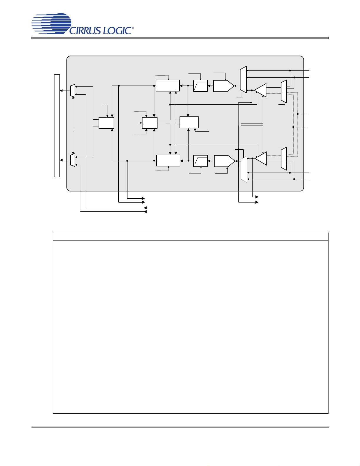
4.2 Analog Inputs
CS42L55
BOOSTA
ADCAMUTE
DIGSFT
ADCAATT[7:0]
ADCB=A
Gain Adjust
DIGSUM[1:0]
Swap/
DIGMUX
PCM Serial Interface
Mix
ALCA
ALCASRDIS
ALCAZCDIS
ALCARATE[5:0]
ALCRRATE[5:0]
MAX[2:0]
MIN[2:0]
ALCB
ALCBSRDIS
ALCBZCDIS
ALC
Gain Adjust
BOOSTB
ADCBMUTE
DIGSFT
ADCBATT[7:0]
ADCB=A
TO DSP Engine
FROM DSP ENGINE
HPFRZA
HPFA
HPFA_CF[1:0]
Noise Gate
`
HPFRZB
HPB
HPFB_CF[1:0]
PDN_ADCA
INV_ADCA
PDN_CHRG
NGALL
NG
THRESH[3:0]
NGDELAY[1:0]
ADC
ADCAMUX[1:0]
ADCBMUX[1:0]
ADC
PDN_ADCB
INV_ADCB
PDN_CHRG
PDN_ADCA
PGAAVOL[5:0]
PGAB=A
ANLGZC
PDN_ADCB
PGABVOL[5:0]
PGAB=A
ANLGZC
PGAAMUX
PGABMUX
ANALOG PASSTHRU TO
HEADPHONE, LINE AMPLIFIER MUX
AIN1A
AIN2A
AIN1REF
AIN2REF
AIN2B
AIN1B
Figure 9. Analog Input Signal Flow
Referenced Control Register Location
Analog Front End
PGAxMUX
PDN_ADCx
PGAxVOL[5:0]
PGAB=A
ANLGZCx
ADCxMUX[1:0]
INV_ADCx
PDN_CHRG
HPFRZx
HPFx
HPFx_CF[1:0]
Digital Volume
BOOSTx
ADCxMUTE
ADCxATT[7:0]
DIGSFT
ADCB=A
ALCx
ALCxSRDIS
ALCxZCDIS
ALCARATE[5:0]
ALCRRATE[5:0]
MAX[2:0]
MIN[2:0]
NGALL
NG
THRESH[3:0]
NGDELAY[1:0]
Miscellaneous
DIGSUM[1:0]
DIGMUX
“PGA x Input Select” on page 49
“Power Down ADC x” on page 42
“PGAx Volume” on page 49
“PGA Channel B=A” on page 48
“Analog Zero Cross” on page 46
“ADC x Input Select” on page 46
“Invert ADC Signal Polarity” on page 48
“Power Down ADC Charge Pump” on page 42
“ADCx High-Pass Filter Freeze” on page 47
“ADCx High-Pass Filter” on page 47
“HPF x Corner Frequency” on page 47
“Boostx” on page 49
“ADC Mute” on page 48
“ADCx Volume” on page 50
“Digital Soft Ramp” on page 46
“ADC Channel B=A” on page 48
“ALCx” on page 62
“ALCx Soft Ramp Disable” on page 65
“ALCx Zero Cross Disable” on page 65
“ALC Attack Rate” on page 63
“ALC Release Rate” on page 63
“ALC Maximum Threshold” on page 64
“ALC Minimum Threshold” on page 64
“Noise Gate All Channels” on page 64
“Noise Gate Enable” on page 65
“Noise Gate Threshold and Boost” on page 65
“Noise Gate Delay Timing” on page 65
“Digital Sum” on page 48
“Digital MUX” on page 45
DS773F1 23
Page 24
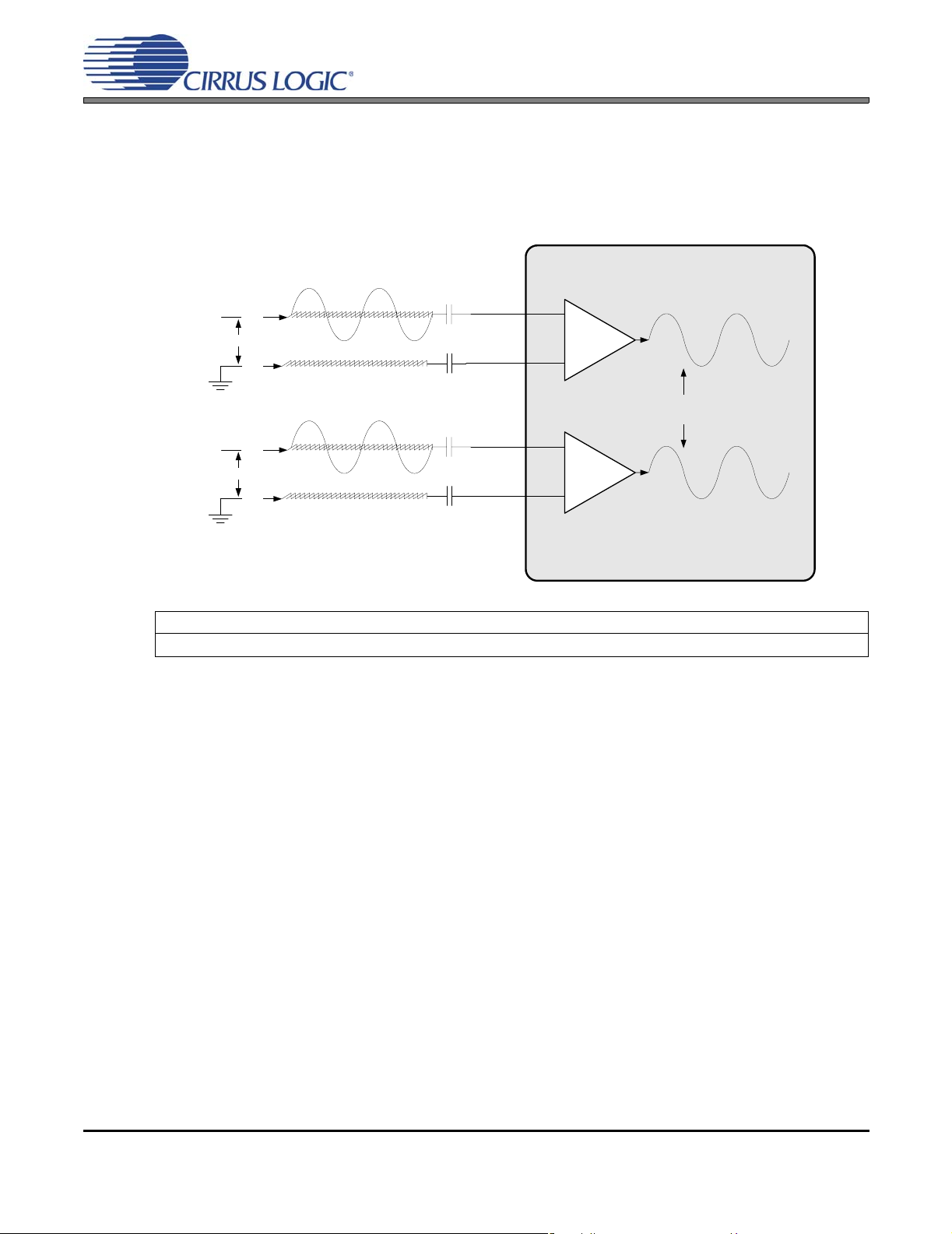
4.2.1 Pseudo-Differential Inputs
The CS42L55 implements a pseudo-differential input stage. The AINxREF inputs are intended to be used
as a pseudo-differential reference signal. This feature provides 0 noise rejection with single-ended signals. Figure 10 shows a basic diagram outlining the internal implementation of the pseudo-differential input stage, including a recommended stereo pseudo-differential input topology. If pseud o-differential input
functionality is not required, simply leave the AINxREF pin floating.
CS42L55
Left Input
(differential traces)
GND
Right Input
(differential traces)
GND
//
//
//
//
Figure 10. Stereo Pseudo-Differential Input
Referenced Control Register Location
PGAxMUX ........................... “PGA x Input Select” on page 49
4.2.2 Automatic Level Control (ALC)
When enabled, the ALC monitors the analog input signal after the digital attenuator. The ALC then detects
when peak levels exceed the maximum threshold settings and first lower s the PGA gain settings and then
increases the digital attenuation levels at a programmable attack rate and maintains the resulting level
below the maximum threshold.
1 µF
1 µF
1 µF
1 µF
AIN1A
AIN1REF
AIN2B
AIN2REF
PGAAMUX=’0'b
26
27
25
24
+
PGA A
-
common mode rejection at input of PGA reduces
+
PGA B
-
PGABMUX=’1'b
external system noise
When input signal levels fall below the minimum threshold, digital attenuation levels are decreased first
and the PGA gain is then increased at a programmable release rate and maintains the resulting level
above the minimum threshold.
Attack and release rates are affected by the ADC soft ramp/zero cross settings and sample rate, Fs. ALC
soft ramp and zero cross dependency may be independently enabled/disabled.
Recommended settings: Best level control may be realized with the fastest attack and slowest release
setting with soft ramp enabled in the control registers.
Notes:
1. When ALC x is enabled and the PGAxVOL[5:0] is set to +12 dB, the ADCxATT[7:0] should not be set
below 0 dB.
2. The maximum desired gain must be set in the PGAxVOL register. The ALC will only apply the gain
set in PGAxVOL.
3. The ALC maintains the output signal between the MIN and MAX thresholds. As the input signal level
changes, the level-controlled output may not always be the same but will always fall between the
thresholds.
24 DS773F1
Page 25

Referenced Control Register Location
PGAxVOL[5:0].....................
ADCxATT[7:0]......................
MAX[2:0], MIN[2:0] ..............
“PGAx Volume” on page 49
“ADCx Volume” on page 50
“ALC Threshold (Address 26h)” on page 64
CS42L55
Input (before ALC)
MIN[2:0]
below full scale
ALC
Response
PGA Gain and/or
Attenuator
Output
(after ALC)
MIN[2:0]
below full scale
RRATE[5:0]
Figure 11. ALC Operation
4.3 Analog In to Analog Out Passthrough
The CS42L55 accommodates analog routing of the analog input signal directly to the headphone and line
out amplifiers. This feature is useful in applications that utilize an FM tuner where audio recovered over-theair must be transmitted to the headphone amplifier without dig ital conversion in the ADC and DAC. This analog passthrough path reduces power consumption and is immu ne to mo dulato r switch ing noise that cou ld
interfere with some tuners. This path is selected using the Line and/or HP mux bits and powering down the
ADC.
Referenced Control Register Location
PDN_ADCx .........................
HPxMUX..............................
LINExMUX...........................
“Power Down ADC x” on page 42
“Headphone Input Select” on page 47
“Line Input Select” on page 47
ARATE[5:0
MAX[2:0]
below full scale
]
MAX[2:0]
below full scale
DS773F1 25
Page 26

4.4 Analog Outputs
INPUTS FROM ADCA
and ADCB
CS42L55
AMIXAMUTE
AMIXBMUTE
AMIXAVOL[6:0]
AMIXBVOL[6:0]
VOL
PMIXAMUTE
PMIXBMUTE
PMIXAVOL[6:0]
PMIXBVOL[6:0]
Demph
DEEMPH
PCM Serial Interface
Digital Mix to ADC
Serial Interface
INV_PCMA
INV_PCMB
OFFTIME[2:0]
ONTIME[3:0]
FREQ[3:0]
BEEP[1:0]
VOL
Generator
PCMASWAP[1:0]
PCMBSWAP[1:0]
Beep
Channel
Swap
*
Figure 12. DSP Engine Signal Flow
Referenced Control Register Location
DSP
PDN_DSP
DEEMPH
PMIXxMUTE
PMIXxVOL[6:0]
INV_PCMx
PCMxSWAP[1:0]
AMIXxMUTE
AMIXxVOL[6:0]
ADCxSWAP[1:0]
MSTxVOL[7:0]
MSTxMUTE
DIGSFT
PLYBCKB=A
TC_EN
BASS_CF[1:0]
TREB_CF[1:0]
BASS[3:0]
TREB[3:0]
Limiter
LIMIT
LIMIT_ALL
LIMSRDIS
LMAX[2:0]
CUSH[2:0]
LIMARATE[7:0]
LIMRRATE[7:0]
Beep Generator
“Power Down DSP” on page 50
“HP/Line De-Emphasis” on page 50
“PCM Mixer Channel x Mute” on page 52
“PCM Mixer Channel x Volume” on page 52
“Invert PCM Signal Polarity” on page 51
“PCM Mix Channel Swap” on page 60
“ADC Mixer Channel x Mute” on page 51
“ADC Mixer Channel x Volume” on page 51
“ADC Mix Channel Swap” on page 60
“Master Volume Control” on page 57
“Master Playback Mute” on page 51
“Digital Soft Ramp” on page 46
“Playback Channels B=A” on page 50
“Tone Control Enable” on page 56
“Bass Corner Frequency” on page 56
“Treble Corner Frequency” on page 55
“Bass Gain” on page 56
“Treble Gain” on page 56
“Peak Detect and Limiter” on page 61
“Peak Signal Limit All Channels” on page 61
“Limiter Soft Ramp Disable” on page 66
“Limiter Maximum Threshold” on page 60
“Limiter Cushion Threshold” on page 61
“Limiter Attack Rate” on page 62
“Limiter Release Rate” on page 62
Refer to “Beep Generator” on page 31 for all referenced controls
Fixed Function DSP
MSTAVOL[7:0]
MSTBVOL[7:0]
Chnl Vol.
Channel
Swap
ADCASWAP[1:0]
ADCBSWAP[1:0]
Σ
BPVOL[4:0]
VOL
MSTxVOL[7:0], MSTxMUTE and DIGSFT are always
available regardless of the PDN_DSP setting.
Settings
Σ
MSTAMUTE
MSTBMUTE
DIGSFT
PLYBCKB=A
VOL
Bass/
Treble/
Control
TC_EN
BASS_CF[1:0]
TREB_CF[1:0]
BASS[3:0]
TREB[3:0]
LIMARATE[7:0]
LIMRRATE[7:0]
LMAX[2:0]
CUSH[2:0]
LIMSRDIS
LIMIT
LIMIT_ALL
Limiter
Peak
Detect
PDN_DSP
*
DAC
to HP and
Line MUX
26 DS773F1
Page 27

CS42L55
ADPTPWR[1:0]
Charge Pump
Step-down/Inverting
CHGFREQ[3:0]
HPxMUX
LINExMUX
+VCP
+VCP/2
-VCP/2
VCP
from PGAx
from DACx
Figure 13. Analog Output Stage
Referenced Control Register Location
Analog Output
ADPTPWR[1:0]
CHGFREQ[3:0]
PDN_HPx[1:0]
PDN_LINx[1:0]
HPxMUTE
HPxVOL[7:0]
LINExMUTE
LINExVOL[7:0]
ANLGZC
PLYBCKB=A
HPxMUX
LINExMUX
“Adaptive Power Adjustment” on page 45
“Charge Pump Frequency” on page 67
“Headphone Power Control” on page 43
“Line Power Control” on page 43
“Headphone Channel x Mute” on page 57
“Headphone Volume Control” on page 57
“Line Channel x Mute” on page 58
“Line Volume Control” on page 58
“Analog Zero Cross” on page 46
“Playback Channels B=A” on page 50
“Headphone Input Select” on page 47
“Line Input Select” on page 47
Class H Control
-VCP
HPxVOL[6:0]
HPxMUTE
ANLGZC
PLYBCKB=A
LINExVOL[6:0]
LINExMUTE
ANLGZC
PLYBCKB=A
= HP and Line Supply
HP Detection HPDETECT
PDN_HPx[1:0]
PDN_LINx[1:0]
+HP Supply +Line Supply
HPREF
-HP Supply -Line Supply
LINEREF
+VHPFILT
HPOUTA
HPOUTB
LINEOUTA
LINEOUTB
-VHPFILT
4.5 Class H Amplifier
The CS42L55 headphone and line output amplifi ers use a patented Cirrus L ogic Bi-Modal Class H te chnology. This technology maximizes operating efficiency of the typical Class AB amplifier while maintaining high
performance. In a Class H amplifier design, the rail voltages supplied to the amplifier vary with the needs of
the music passage that is being amplified. This prevents unnecessarily wasting energy during low power
passages of program material or when the program material is played back at a low volume level.
The central component of the Bi-Modal Class H technology found in the CS42L55 is the internal charge
pump, which creates the rail voltages for the headphone and line amplifiers of th e device. The charge pump
receives its input voltage from the voltage present on the VCP pin of the CS42L55. From this input voltage,
the charge pump creates the differential rail voltages that are supplied to the amplifier output stages. The
charge pump is capable of supplying two sets of differential rail voltages. One set is equal to ± VCP and the
other is equal to ± VCP/2.
4.5.1 Power Control Options
The method by which the CS42L55 decides which set of rail voltages is supplied to the amplifier output
stages depends on the settings of the Adaptive Power bits (ADPTPWR) found in “Class H Power Control
(Address 06h)” section on pa ge 45. As detailed in this section, there are four possible settings for these
bits: Mode 00, 01, 10 and 11.
Referenced Control Register Location
ADPTPWR[1:0]................... “Adaptive Power Adjustment” on page 45
DS773F1 27
Page 28

CS42L55
4.5.1.1 Standard Class AB Operation (Mode 01 and 10)
When the Adaptive Power bits are set to either 01 or 10, the rail voltages supplied to the amplifiers will be
held to ±VCP/2 or ±VCP, respectively. For these two settings, the rail voltages supplied to the output stages are held constant, regardless of the signal level, internal volume se ttings, or the settings of the AIN and
DIN advisory volume registers. In either of these two settings, the amplifiers in the CS42L 55 simply operate in a traditional Class AB configuration.
4.5.1.2 Adapted to Volume Settings (Mode 00)
When the Adaptive Power bits are set to 00, the CS42L55 decides which set of rail voltages to send to
the amplifiers based upon the gain and attenuation levels of all active inter nal processing blocks. In order
to adjust for external analog (line or microphone sources) or digital (DSP) input volume settings, it also
takes into account the settings of the AIN and DIN advisory volume registers. The combined effect of all
volume settings is shown in Figure 14.
Analog Input Source
I²S Serial Audio Input
Control Port
Amplifier
Headphone
External DSP
PMIX, AMIX
Volume
Setting
Master
Volume
Setting
Headphone or
Line Volume
Setting
AIN Advisory
Volume Setting
DIN Advisory
Volume Setting
Control Logic
Charge
Pump
Line
Amplifier
Figure 14. Adaptive Mode 00
If the total gain and attenuation set in the volume control registers would cause the amplifiers to clip a fullscale signal when operating from the lower set of rail voltages, the control logic instructs the charge pump
to provide the higher set of the two rail voltages (±VCP) to the amplifiers. If the total gain and attenuation
set in the volume control registers would not cause the amplifiers to clip a full-scale signal when operating
from the lower set of rail voltages, the control logic instructs the charge pump to supply the lower set of
rail voltages (±VCP/2) to the amplifiers.
Note: The A and B channels of each respective volume control must both cross the thr eshold to trigger
a change in the VCP mode. The control logic also monitors various functions (listed in the table below)
that may affect the total gain and attenuation of the signal applied to the amplifiers.
28 DS773F1
Page 29

Referenced Control Register Location
HPxVOL[7:0] .......................
LINExVOL[7:0] ....................
MSTxVOL[7:0].....................
MSTxMUTE.........................
AMIXxVOL[6:0]....................
PMIXxVOL[6:0]....................
AINADV[7:0]........................
DINADV[7:0]........................
BOOSTx..............................
ADCxMUX...........................
PGAxVOL............................
ADCxMUTE.........................
ADCxSWP...........................
PCMxSWP ..........................
HPxMUX..............................
LINExMUX...........................
HPxMUTE ...........................
LINExMUTE ........................
PDN_HPx............................
PDN_LINEx.........................
TREB...................................
BASS...................................
TCEN...................................
BEEP...................................
BPVOL ................................
ADCB=A..............................
PGAB=A..............................
PLYBCKB=A........................
“Headphone Volume Control” on page 57
“Line Volume Control” on page 58
“Master Volume Control” on page 57
“Master Playback Mute” on page 51
“ADC Mixer Channel x Volume” on page 51
“PCM Mixer Channel x Volume” on page 52
“Analog Input Advisory Volume” on page 59
“Digital Input Advisory Volume” on page 59
“Boostx” on page 49
“ADC x Input Select” on page 46
“PGAx Volume” on page 49
“ADC Mute” on page 48
“ADC Mix Channel Swap” on page 60
“PCM Mix Channel Swap” on page 60
“Headphone Input Select” on page 47
“Line Input Select” on page 47
“Headphone Channel x Mute” on page 57
“Line Channel x Mute” on page 58
“Headphone Power Control” on page 43
“Line Power Control” on page 43
“Treble Gain” on page 56
“Bass Gain” on page 56
“Tone Control Enable” on page 56
“Beep Configuration” on page 55
“Beep Volume” on page 55
“ADC Channel B=A” on page 48
“PGA Channel B=A” on page 48
“Playback Channels B=A” on page 50
CS42L55
4.5.1.3 Adapted to Output Signal (Mode 11)
When the Adaptive Power bits are set to 11, the CS42L55 decides which of the two sets of rail voltages
to send to the amplifiers based solely upon the level of the signal being sent to the amplifiers. If the signal
that is sent to the amplifiers would cause the amplifiers to clip when operating on the lower set of rail voltages, the control logic instructs the charge pump to provide the higher set of rail voltages (±VCP) to the
amplifiers. If the signal that is sent to the amplifiers would not cause the amplifiers to clip when o perating
on the lower set of rail voltages, the control logic instructs the charge pump to provide the lower set of rail
voltages (±VCP/2) to the amplifiers. This mode of operation eliminates the need to advise the CS42L55
of volume settings external to the device.
Note: Signal detection is made using digital circuitry. This mode should, ther efore, not be used with analog passthrough (PGA to HP/Line).
4.5.2 Power Supply Transitions
Charge pump transitions from the lower set of rail voltages to the higher set of rail voltages occur on the
next FLYN/P clock cycle. Despite the fast response time of the system, the capacitive elements on the
VHPFILT pins prevent the rail voltages from changing instantaneously. Instead, the rail voltages ramp up
from ±VCP/2 to ±VCP based on the time constant created by the output impedance of the charge pump
and the capacitor on the VHPFILT pin (the transition time is approximately 20 µs). This behavior is detailed in Figure 15. During this charging transition, a high dv/dt transient on the inputs may briefly clip the
outputs before the rail voltages charge to the full ±VCP level. This transitory clipping has been found to
be inaudible in listening tests.
DS773F1 29
Page 30

CS42L55
Ideal Transition
+VCP
+VCP
2
-VCP
2
-VCP
Ideal Transition
When the charge pump transitions from the high er set of rail voltages to the lower se t, there is a one second delay before the charge pump supplies the lower rail voltages to the amplifiers. This hysteresis ensures that the charge pump doesn't toggle between the two rail voltages as signals approach the clip
threshold. It also prevents clipping in the instance of repetitive high level transients in the input signal. The
timing diagram for this transitional behavior is detailed in Figure 16.
Actual Transition caused
by VHPFILT Capacitor
Actual Transition caused
by VHPFILT Capacitor
Figure 15. VHPFILT Transitions
Time
Output Level
-10 dB
Amplifier Rail
Voltage
VCP
VCP
2
- VCP
2
- VCP
1 second
Time
Time
Figure 16. VHPFILT Hysteresis
30 DS773F1
Page 31

4.5.3 Efficiency
As discussed in previous sections, the amplifiers inte rnal to the CS42L 55 operate fro m one of two sets of
rail voltages, based upon the needs of the signal bei ng amplified or the total gain/attenuation settings. The
power curves for the two mo des of o peration are show n in Figure 15. This graph details the power supplied to a load versus the power drawn from the supply for each of the three use cases.
All Supplies= 1.8 V
= 32 Ω
R
L
Class AB Amplifiers do not
conserve power with typical
headphone loads.
Class H Amplifiers automatically
switch between ±VCP and ±VCP/2
to conserve power with typical
headphone loads.
CS42L55
±VCP
±VCP/2
Figure 17. Class H Power to Load vs. Power from VCP Supply
When the rail voltages are set to VCP, the amplifiers will operate in their least efficient mode. When the
rail voltages are held at ±VCP/2, the amplifiers will operate in their most efficient mode, but will be will
clipped if required to amplify a full-scale signal.
Note: The ±VCP/2 curve ends at the point at which the output of the amplifiers reached 10% THD+N.
The benefit of Bi-Modal Class H is shown in the solid trace on the graph. At lower output levels, the am -
plifiers operate on the ±VCP/2 curve. At higher output le vels, they ope rate on the ±VCP cur ve. The du ration the amplifiers will operate on either of the two curves (±VCP/2 or ±VCP) depends on both the content
and the output level of the program material being amplified. The highest efficiency operation will result
from maintaining an output level that is close to, but not exceeding, the clip threshold of the ±VCP/2 curve.
4.6 Beep Generator
The Beep Generator generates audio frequencies across approximately two octave major scales. It offers
three modes of operation: Continuous, multiple and single (one -shot) beeps. Sixteen On and eight Off times
are available.
Note: The Beep is generated before the limiter and may affect desired limiting performance. If the limiter
function is used, it may be necessary to set the beep volume sufficiently below the threshold to prevent the peak detect from triggering. Since the master volume control, MSTxVOL[7:0], will affect
the beep volume, the DAC volume may alternatively be controlled using the PMIXxVOL[6:0] bits.
DS773F1 31
Page 32
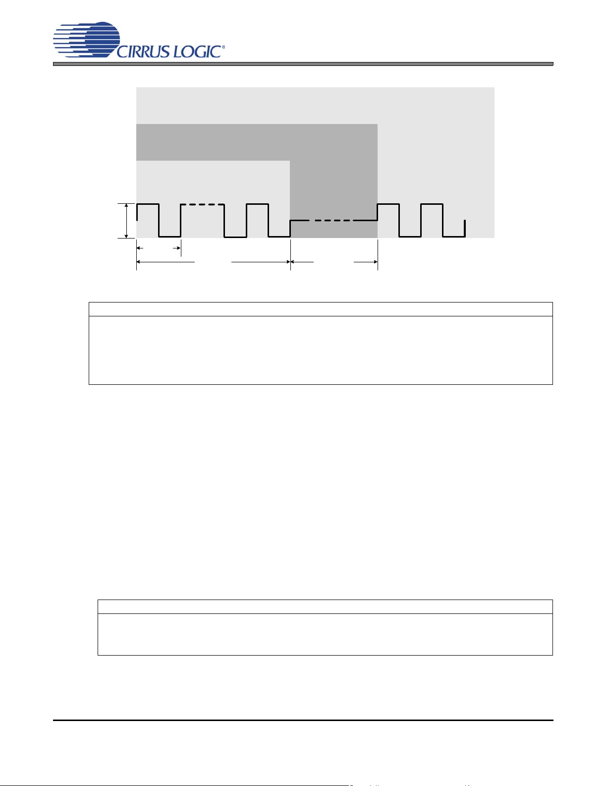
CS42L55
BEEP[1:0] =
'11'
CONTINUOUS BEEP: Beep turns on at a configurable frequency (FREQ) and volume (BPVOL) and remains on
until REPEAT is cleared.
BPVOL[4:0]
Referenced Control Register Location
MSTxVOL[7:0].....................
PMIXxVOL[6:0]....................
OFFTIME[2:0]......................
ONTIME[3:0] .......................
FREQ[3:0] ...........................
BEEP[1:0]............................
BPVOL[4:0] .........................
4.7 Limiter
BEEP[1:0] =
'10'
BEEP[1:0] =
'01'
FREQ[3:0]
MULTI-BEEP: Beep turns on at a configurable frequency (FREQ)
and volume (BPVOL) for the duration of ONTIME and turns off for
the duration of OFFTIME. On and off cycles are repeated until
REPEAT is cleared.
SINGLE-BEEP: Beep turns on at a
configurable frequency (FREQ) and
volume (BPVOL) for the duration of
ONTIME. BEEP must be cleared
and set for additional beeps.
ONTIME[3:0] OFFTIME[2:0]
Figure 18. Beep Configuration Options
“Master Volume Control: MSTA (Address 18h) & MSTB (Address 19h)” on page 57
“PCMx Mixer Volume: PCMA (Address 12h) & PCMB (Address 13h)” on page 52
“Beep Off Time” on page 54
“Beep On Time” on page 54
“Beep Frequency” on page 53
“Beep Configuration” on page 55
“Beep Volume” on page 55
...
When enabled, the limiter monitors the digital input signal before the DAC modulators, detects when levels
exceed the maximum threshold settings and lowers the master volume at a pr ogrammable attack rate below
the maximum threshold. When the input signal level falls below the maximum threshold, the AOUT volume
returns to its original level set in the Master Volume Control register at a programmable release r ate. Attack
and release rates are affected by the DAC soft ramp settings and sa mple rate, Fs. Limiter soft r amp dependency may be independently enabled/disab l ed using th e LIM S R D IS.
Notes:
1. Recommended settings: Best limiting performance may be realized with the fastest attack and
slowest release setting with soft ramp enabled in the control registers. The CUSH bits allow the user
to set a threshold slightly below the maximum threshold for hysteresis control - this cushions the
sound as the limiter attacks and releases.
2. The Limiter maintains the output signal between the CUSH and MAX thresholds. As the digital input
signal level changes, the level-controlled output may not always be the same but will always fall within
the thresholds.
Referenced Control Register Location
Limiter Rates.......................
Limiter Thresholds
LIMSRDIS...........................
Master Volume Control........
“Limiter Release Rate” on page 62, “Limiter Attack Rate” on page 62
“Limiter Maximum Threshold” on page 60, “Limiter Cushion Threshold” on page 61
“Limiter Soft Ramp Disable” on page 66
“Master Volume Control: MSTA (Address 18h) & MSTB (Address 19h)” on page 57
32 DS773F1
Page 33

Input
MAX[2:0]
Limiter
Output
(after Limiter)
MAX[2:0]
Volume
ATTACK/RELEASE SOUND
CUSHION
CS42L55
CUSH[2:0]
RRATE[5:0]ARATE[5:0]
Figure 19. Peak Detect & Limiter
DS773F1 33
Page 34
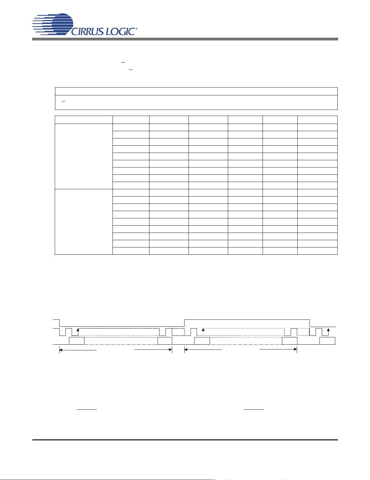
4.8 Serial Port Clocking
The CODEC serial audio interface port operates either as a slave or master. It accepts externally generated
clocks in Slave Mode (M/S
(MCLK) in Master Mode (M/S
ciated with a given MCLK and sample rate.
Referenced Control Register Location
Register 05h........................
......................................
M/S
MCLK (MHz) LRCK (kHz) Clock Ratio SPEED[1:0] 32kGROUP RATIO[1:0] Register 05h
12.0000
(MCLKDIV2=’1’b)
6.0000
(MCLKDIV2=’0’b)
CS42L55
= ‘0’b) and will generate synchronous clocks derived from an input master clock
= ‘1’b). Refer to the table below for the required setting in register 05h asso-
“Clocking Control 2 (Address 05h)” on page 44
“Master/Slave Mode” on page 43
8.0000 1500 11 1 01 0x1D
11.0294 1088 11 0 11 0x1B
12.0000 1000 11 0 01 0x19
16.0000 750 10 1 01 0x15
22.0588 544 10 0 11 0x13
24.0000 500 10 0 01 0x11
32.0000 375 01 1 01 0x0D
44.1180 272 01 0 11 0x0B
48.0000 250 01 0 01 0x09
8.0000 750 11 1 01 0x1D
11.0294 544 11 0 11 0x1B
12.0000 500 11 0 01 0x19
16.0000 375 10 1 01 0x15
22.0588 272 10 0 11 0x13
24.0000 250 10 0 01 0x11
32.0000 187.5 01 1 01 0x0D
44.1180 136 01 0 11 0x0B
48.0000 125 01 0 01 0x09
4.9 Digital Interface Format
The serial port operates in the I²S digital interface formats with varying bit depths up to 24 into the DAC and
a fixed depth of 24 out the ADC. Data is clocked out of the ADC on an internally delayed version of the rising
SCLK edge. This provides more setup time for capturing data on the rising edge of SCLK. Data is clocked
into the DAC on the rising edge of SCLK.
LRCK
SCLK
SDIN
SDOUT
MSB LSB LSB
Left Channel Right Channel
AOUTA / AINxA
4.10 Initialization
The CODEC enters a Power-Down state upon initial power-up. The interpolation and decimation filters, delta-sigma modulators and control port registers are reset. The charge pump, LDO, internal voltage reference
and switched-capacitor low-pass filters are powered down. The device will remain in the Power-Down state
until the RESET
ister settings can be loaded per the interface descriptions in the “Register Description” on page 42.
pin is brought high. The control port is accessible once RESET is high and the desired reg-
MSB MSB
AOUTB / AINxB
Figure 20. I²S Format
34 DS773F1
Page 35

After the PDN bit is released and MCLK is valid, the quiescent voltage, VQ, and the internal voltage reference, FILT+, will begin powering up to normal operation. The charge pump slowly powers up and charges
the capacitors. Power is then applied to the headphone amplifiers and switched-capacitor filters, and the analog/digital outputs enter a muted state. MCLK occurrences are counted over one LRCK period to determine
a valid MCLK/LRCK ratio and normal operation begins.
4.11 Recommended DAC to HP or Line Power-Up Sequence (Playback)
1. Hold RESET low until the power supplies are stable; no specific power supply sequencing is required.
RESET
2. Apply MCLK (LRCK, SCLK and SDIN may be applied at any time) at the appropriate frequency.
3. Bring RESET
4. Wait a minimum of 500 ns before writing to the control port.
5. The default state of the master power down bit, PDN, is ‘1’b. Load the following register settings while
keeping the PDN bit set to ‘1’b.
6. Load the required register settings detailed in 4.13 “Required Initialization Settings” on page 37.
7. Configure the headphone and line power down controls for ON, OFF, or HPDETECT operation.
Register Controls: PDN_HPx[1:0], PDN_LINx[1:0]
8. Configure the serial port I/O control for master or slave operation.
Register Controls: M/S
9. Configure the master clock (MCLK) and bit clock (SCLK) I/O control as desired. Refer to 4.8 “Serial Port
Clocking” on page 34 for the required configuration for a given master clock.
Register Controls: MCLKDIV2, SCK=MCK
10. Configure the sample rate (LRCK) controls for the desired sample rate. Refer to 4.8 “Serial Port Clock-
ing” on page 34 for the required configuration for a given sample rate.
Register Controls: See Register 05h
11. The default state of the DSP engine’s power down bit, PDN_DSP, is ‘0’b. It is not necessary to power
down the DSP before changing the various DSP functions. The DSP may be powered down for additional power savings.
12. To minimize pops on the headphone or line amplifier, each respective analog volume control must first
be muted and set to maximum attenuation.
Register Controls: HPxMUTE, LINExMUTE, HPxVOL[6:0], LINExVOL[6:0]
13. After muting the headphone or line amplifiers, set the PDN bit to ‘0’b.
14. Wait 75 ms for the headphone or line amplifier to power up.
15. Un-mute and ramp the volume for the headphone or line amplifiers to the desired level.
16. Bring RESET
prevent power glitch related issues.
Power Up Sequence Register Location
Step 5, 13............................
Step 7..................................
Steps 8-9 .............................
Step 10................................
Step 11................................
Step 12a,15a.......................
Step 12b,15b.......................
should be held low for a minimum of 1 ms after power supplies are stable.
high.
low if the analog or digital supplies drop below the recommended operating condition to
“Power Down” on page 42
“Power Control 2 (Address 03h)” on page 43
“Clocking Control 1 (Address 04h)” on page 43
“Clocking Control 2 (Address 05h)” on page 44
“Power Down DSP” on page 50
“Headphone Channel x Mute” on page 57, “Line Channel x Mute” on page 58
“Headphone Volume Control” on page 57, “Line Volume Control” on page 58
CS42L55
DS773F1 35
Page 36
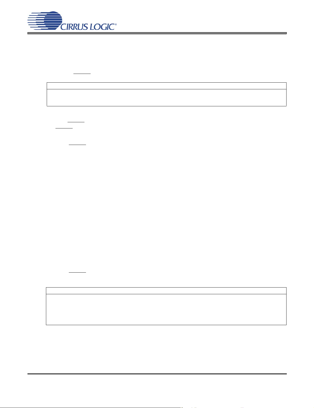
CS42L55
4.11.1 Recommended Power-Down Sequence
1. To minimize pops on the headphone or line amplifier, each respective analog volume control must
first be muted and set to maximum attenuation.
Register Controls: HPxMUTE, LINExMUTE, HPxVOL[6:0], LINExVOL[6:0]
2. Set the PDN bit to ‘1’b.
3. Bring RESET
Power Down Sequence Register Location
Step 1a ................................
Step 1b ................................
Step 2 ..................................
4.12 Recommended PGA to HP or Line Power-Up Sequence (Analog Passthrough)
1. Hold RESET low until the power supplies are stable; no specific power supply sequencing is required.
RESET
2. Apply MCLK at the appropriate frequency.
3. Bring RESET
4. Wait a minimum of 500 ns before writing to the control port.
5. The default state of the master power down bit, PDN, is ‘1’b. Load the following register settings while
keeping the PDN bit set to ‘1’b.
6. Load the required register settings detailed in 4.13 “Required Initialization Settings” on page 37.
7. Configure the headphone and line power down controls for ON, OFF, or HPDETECT operation.
Register Controls: PDN_HPx[1:0], PDN_LINx[1:0]
8. Configure the HP and/or Line amplifiers to receive the analog output from the PGA.
Register Controls: LINExMUX, HPxMUX
9. Power down the DSP engine.
Register Controls: PDN_DSP
10. To minimize pops on the headphone or line amplifier, each respective analog volume control must first
be muted and set to maximum attenuation.
Register Controls: HPxMUTE, LINExMUTE, HPxVOL[6:0], LINExVOL[6:0]
11. After muting the headphone and/or line amplifiers, set the PDN bit to ‘0’b.
12. Wait 75 ms for the headphone or line amplifier to power up.
13. Un-mute and ramp the volume for the headphone or line amplifiers to the desired level.
14. B ring RESET
prevent power glitch related issues.
Power Up Sequence Register Location
Step 5, 11............................
Step 7..................................
Steps 8 ................................
Step 9..................................
Step 10a,13a.......................
Step 10b,13b.......................
should be held low for a minimum of 1 ms after power supplies are stab le.
low.
“Headphone Volume Control” on page 57, “Line Volume Control” on page 58
“Headphone Channel x Mute” on page 57, “Line Channel x Mute” on page 58
“Power Down” on page 42
high.
low if the analog or digital supplies drop below the recommended operating condition to
“Power Down” on page 42
“Power Control 2 (Address 03h)” on page 43
“ADC, Line, HP MUX (Address 08h)” on page 46
“Power Down DSP” on page 50
“Headphone Channel x Mute” on page 57, “Line Channel x Mute” on page 58
“Headphone Volume Control” on page 57, “Line Volume Control” on page 58
4.12.1 Recommended Power-Down Sequence
1. To minimize pops on the headphone and/or line amplifier, each respective analog volume control
must first be muted and set to maximum attenuation.
Register Controls: HPxMUTE, LINExMUTE, HPxVOL[6:0], LINExVOL[6:0]
2. During power down, the CODEC attempts to power down on a zero cross transition of the analog
36 DS773F1
Page 37
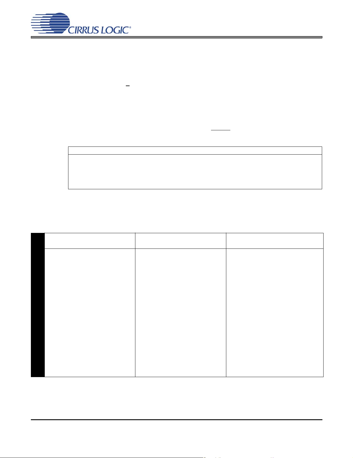
CS42L55
signal. The zero cross timeout, however, is dependent on the ser ial p or t cl ock dom ain. Thu s, to fu lly
power down, the ADC must briefly power up to enable the zero cross state machine. Follow the
remaining steps below to complete the power down sequence.
3. Set bit 5 in register 07h to ‘1’b. This implements a high impedance state on the serial output ports to
avoid possible contention in step 4 if clocks are already applied to the serial port.
4. Configure the serial port I/O control for master operation.
Register Controls: M/S
5. Power up either one of the ADC channels.
Register Controls: PDN_ADCx
6. Wait 100 ms.
7. Set the PDN bit to ‘1’b. The CODEC is completely powered down in a low power state.
8. To achieve the lowest operating quiescent current, bring RESET
reset to their default state.
Power Down Sequence Register Location
Step 1a................................
Step 1b................................
Step 3..................................
Step 4..................................
Step 5..................................
Step 7..................................
“Headphone Volume Control” on page 57, “Line Volume Control” on page 58
“Headphone Channel x Mute” on page 57, “Line Channel x Mute” on page 58
“Miscellaneous Control (Address 07h)” on page 45
“Master/Slave Mode” on page 43
“Power Down ADC x” on page 42
“Power Down” on page 42
low. All control port registers will be
4.13 Required Initialization Settings
The current required for various sections in the CODEC must be reduced using the control port compensation strategy shown below. All performance and power consumption measurements were taken with the
Control Port Compensation shown below.
VA < 2.1 V VA > 2.1 V Current adjustments are made in
1. Write 0x99 to register 0x00.
2. Write 0x30 to register 0x2E.
3. Write 0x07 to register 0x32.
4. Write 0xFF to register 0x33.
5. Write 0xF8 to register 0x34.
6. Write 0xDC to register 0x35.
7. Write 0xFC to register 0x36.
8. Write 0xAC to register 0x37.
Control Port
9. Write 0xF8 to register 0x3A.
Compensation
10. Write 0xD3 to register 0x3C.
11. Write 0x23 to register 0x3D.
12. Write 0x81 to register 0x3E.
13. Write 0x46 to register 0x3F.
14. Write 0x00 to register 0x00.
1. Write 0x99 to register 0x00.
2. Write 0x30 to register 0x2E.
3. Write 0x07 to register 0x32.
4. Write 0xFD to register 0x33.
5. Write 0xF8 to register 0x34.
6. Write 0xDC to register 0x35.
7. Write 0xF8 to register 0x36.
8. Write 0x6C to register 0x37.
9. Write 0xF8 to register 0x3A.
10. Write 0xD3 to register 0x3C.
11. Write 0x23 to register 0x3D.
12. Write 0x81 to register 0x3E.
13. Write 0x46 to register 0x3F.
14. Write 0x00 to register 0x00.
the following sections:
1. [Enable test register access.]
2. Digital Regulator.
3. ADC.
4. ADC.
5. ADC.
6. Zero Cross Detector.
7. PGA.
8. PGA.
9. DAC.
10. Headphone Amplifier.
11. Headphone & Line Amplifier.
12. Line Amplifier.
13. PGA & ADC.
14. [Disable test register access.].
DS773F1 37
Page 38
4.14 Control Port Operation
The control port is used to access the registers allowing the CODEC to be configure d for the desired operational modes and formats. The operation of the control port ma y be completely asynchron ous with respect
to the audio sample rates. However, to avoid potential interference problems, the control port pins should
remain static if no operation is required.
The control port operates using an I²C interface with the CODEC acting as a slave device.
4.14.1 I²C Control
SDA is a bidirectional data line. Data is clocked into and out of the part by the clock, SCL. The signal timings for a read and write cycle are shown in Figure 21 and Figure 22. A Start condition is def ined as a
falling transition of SDA while the clock is high. A Stop condition is defined as a rising transition of SDA
while the clock is high. All other transitions of SDA occur while the clock is low. The first byte sent to the
CS42L55 after a Start condition consists of a 7-bit chip address field and a R/W
for a write).
The upper 7 bits of the address field are fixed at 1001010. To communicate with the CS42L55, the chip
address field, which is the first byte sent to the CS42L55, should match 1001010. The eighth bit of the
address is the R/W
MAP selects the register to be read or written. If the operation is a read, th e contents of the register pointed
to by the MAP will be output. Setting the auto-increment bit in MAP allows successive reads or writes of
consecutive registers. Each byte is se parated by an acknowledge bit. The ACK bit is output from the
CS42L55 after each input byte is read and is input to the CS42L55 from the microcontroller after each
transmitted byte.
bit. If the operation is a write, the next byte is the Memory Address Pointer (MAP); the
CS42L55
bit (high for a read, low
SCL
SDA
SCL
SDA
0 1 2 3 8 9 12 16 17 18 19 10 11 13 14 15 27 28
CHIP ADDRESS (WRITE) MAP BYTE DATA
1 0 0 1 0 1 0 0
START
4 5 6 7 24 25
INCR 6 5 4 3 2 1 0 7 6 1 0 7 6 1 0 7 6 1 0
ACK
26
DATA +1
DATA +n
ACKACKACK
Figure 21. Control Port Timing, I²C Write
2 3 10 11 17 18 19 25
CHIP ADDRESS (WRITE)
1 0 0 1 0 1 0 0
START
MAP BYTE
INCR 6 5 4 3 2 1 0
ACK
16 8 9 12 13 14 15 4 5 6 7 0 1 20 21 22 23 24
STOP
ACK
START
CHIP ADDRESS (READ)
1 0 0 1 0 1 0 1
26 27 28
DATA
7 0 7 0 7 0
ACK
DATA +1
ACK
DATA + n
NO
ACK
Figure 22. Control Port Timing, I²C Read
Since the read operation cannot set the MAP, an aborted write operation is used as a preamble. As shown
in Figure 22, the write operation is aborted (after the acknowledge for the MAP byte) by sending a stop
condition. The following pseudocode illustrates an aborted write operation followed by a read operation.
Send start condition.
Send 10010100 (chip address & write operation).
Receive acknowledge bit.
Send MAP byte, auto-increment off.
STOP
STOP
38 DS773F1
Page 39

Receive acknowledge bit.
Send stop condition, aborting write.
Send start condition.
Send 10010101 (chip address & read operation).
Receive acknowledge bit.
Receive byte, contents of selected register .
Send acknowledge bit.
Send stop condition.
Setting the auto-increment bit in the MAP allows successive reads or writes of consecutive registers. Each
byte is separated by an acknowledge bit.
4.14.2 Memory Address Pointer (MAP)
The MAP byte comes after the address byte and selects the register to be read or written. Refer to the
pseudo code above for implementation details.
4.14.2.1 Map Increment (INCR)
The device has MAP auto-increment capability enabled by the INCR bit (the MSB) of the MAP. If INCR is
set to 0, MAP will stay constant for successive I²C writes or reads. If INCR is set to 1, MAP will auto-increment after each byte is read or written, allowing block reads or writes of successive registers.
CS42L55
DS773F1 39
Page 40

CS42L55
5. REGISTER QUICK REFERENCE
(Default values are shown below the bit names)
I²C Address: 1001010[R/W] - 10010100 = 0x94(Write); 10010101 = 0x95(Read)
Adr.
01h
p42 xxxxxxxx
02h
p42 00001111
03h
p43 11111111
04h
p43 00000000
05h
p44 00001011
06h
p45 00000000
07h
p45 00001100
08h
p46 00000000
09h
p47 10100000
0Ah
p48 00000000
0Bh
p49 00000000
0Ch
p49 00000000
0Dh
p50 00000000
0Eh
p50 00000000
0Fh
p50 00000000
10h
p51 10000000
11h
p51 10000000
12h
p52 00000000
13h
p52 00000000
14h
p53 00000000
15h
p54 00000000
16h
p55 00000000
17h
p56 10001000
18h
p57
19h
p57
1Ah
p57 00000000
Function 7 6 5 4 3 2 1 0
ID
(Read Only)
Power Ctl 1
Power Ctl 2
Clocking Ctl 1
Clocking Ctl 2
Class H Power
Ctl
Misc. Ctl
ADC, Line, HP
MUX
HPF Ctl
Misc. ADC Ctl
PGAA Vol, MUX
PGAB Vol, MUX
ADCA Attenua-
tor
ADCB Attenua-
tor
Playback Ctl 1
ADCMIXA Vol
ADCMIXB Vol
PCMMIXA Vol
PCMMIXB Vol
BEEP Freq,
On Time
BEEP Vol,
Off Time
BEEP,
Tone Cfg.
Tone Ctl
Master A Vol
Master B Vol
Headphone A
Volume
Reserved Reserved Reserved Reserved Reserved REVID2 REVID1 REVID0
Reserved Reserved Reserved Reserved PDN_CHRG PDN_ADCB PDN_ADCA PDN
PDN_HPB1 PDN_HPB0 PDN_HPA1 PDN_HPA0 PDN_LINB1 PDN_LINB0 PDN_LINA1 PDN_LINA0
Reserved Reserved M/S
Reserved Reserved Reserved SPEED1 SPEED0 32kGROUP RATIO1 RATIO0
Reserved Reserved ADPTPWR1 ADPTPWR0 Reserved Reserved Reserved Reserved
DIGMUX Reserved Reserved Reserved ANLGZC DIGSFT Reserved FREEZE
ADCBMUX1 ADCBMUX0 ADCAMUX1 ADCAMUX0 LINEBMUX LINEAMUX HPBMUX HPAMUX
HPFB HPFRZB HPFA HPFRZA HPFB_CF1 HPFB_CF0 HPFA_CF1 HPFA_CF0
ADCB=A PGAB=A DI GSUM1 DIGSUM0 INV_ADCB INV_ADCA ADCBMUTE ADCAMUTE
BOOSTA PGAAMUX PGAAVOL5 PGAAVOL4 PGAAVOL3 PGAAVOL2 PGAAVOL1 PGAAVOL0
BOOSTB PGABMUX PGABVOL5 PGABVOL4 PGABVOL3 PGABVOL2 PGABVOL1 PGABVOL0
ADCAATT7 ADCAATT6 ADCAATT5 ADCAATT4 ADCAATT3 ADCAATT2 ADCAATT1 ADCAATT0
ADCBATT7 ADCBATT6 ADCBATT5 ADCBATT4 ADCBATT3 ADCBATT2 ADCBATT1 ADCBATT0
PDN_DSP DEEMPH Reserved PLYBCKB=A INV_PCMB INV_PCMA MSTBMUTE MSTAMUTE
AMIXAMUTE AMIXAVOL6 AMIXAVOL5 AMIXAVOL4 AMIXAVOL3 AMIXAVOL2 AMIXAVOL1 AMIXAVOL0
AMIXBMUTE AMIXBVOL6 AMIXBVOL5 AMIXBVOL4 AMIXBVOL3 AMIXBVOL2 AMIXBVOL1 AMIXBVOL0
PMIXAMUTE PMIXAVOL6 PMIXAVOL5 PMIXAVOL4 PMIXAVOL3 PMIXAVOL2 PMIXAVOL1 PMIXAVOL0
PMIXBMUTE PMIXBVOL6 PMIXBVOL5 PMIXBVOL4 PMIXBVOL3 PMIXBVOL2 PMIXBVOL1 PMIXBVOL0
FREQ3 FREQ2 FREQ1 FREQ0 ONTIME3 ONTIME2 ONTIME1 ONTIME0
OFFTIME2 OFFTIME1 OFFTIME0 BPVOL4 BPVOL3 BPVOL2 BPVOL1 BPVOL0
BEEP1 BEEP0 Reserved TREB_CF1 TREB_CF0 BASS_CF1 BASS_CF0 TC_EN
TREB3 TREB2 TREB1 TREB0 BASS3 BASS2 BASS1 BASS0
MSTAVOL7 MSTAVOL6 MSTAVOL5 MSTAVOL4 MSTAVOL3 MSTAVOL2 MSTAVOL1 MSTAVOL0
00000000
MSTBVOL7 MSTBVOL6 MSTBVOL5 MSTBVOL4 MSTBVOL3 MSTBVOL2 MSTBVOL1 MSTBVOL0
00000000
HPAMUTE HPAVOL6 HPAVOL5 HPAVOL4 HPAVOL3 HPAVOL2 HPAVOL1 HPAVOL0
INV_SCLK SCK=MCK1 SCK=MCK0 MCLKDIV2 MCLKDIS
40 DS773F1
Page 41

CS42L55
I²C Address: 1001010[R/W
Adr.
1Bh
p57 000 0000 0
1Ch
p58 000 0000 0
1Dh
p58 000 0000 0
1Eh
p59 000 0000 0
1Fh
p59 000 0000 0
20h
p60 000 0000 0
21h
p60 000 0000 0
22h
p61 011 1111 1
23h
p62 000 0000 0
24h
p62 000 0000 0
25h
p63 001 1111 1
26h
p64 000 0000 0
27h
p64 000 0000 0
28h
p65 000 0000 0
29h
p66 000 0000 0
2Ah
p67 000 0010 1
Function 7 6 5 4 3 2 1 0
Headphone B
Volume
Line A
Volume
Line B
Volume
Analog Input
Advisory Vol
Digital Input
Advisory Vol
Channel Mixer
& Swap
Limit Thresholds
Limit Ctl,
Release Rate
Limiter Attack
Rate
ALC Enable,
Attack Rate
ALC Release
Rate
ALC Thresholds
Noise Gate Ctl
ALC, Limiter
SFT, ZC Disable
Misc. Status
(Read Only)
Charge Pump
Freq
] - 10010100 = 0x94(Write); 10010101 = 0x95(Read)
HPBMUTE HPBVOL6 HPBVOL5 HPBVOL4 HPBVOL3 HPBVOL2 HPBVOL1 HPBVOL0
LINEAMUTE LINEAVOL6 LINEAVOL5 LINEAVOL4 LINEAVOL3 LINEAVOL2 LINEAVOL1 LINEAVOL0
LINEBMUTE LINEBVOL6 LINEBVOL5 LINEBVOL4 LINEBVOL3 LINEBVOL2 LINEBVOL1 LINEBVOL0
AINADV7 AINADV6 AINADV5 AINADV4 AINADV3 AINADV2 AINADV1 AINADV0
DINADV7 DINADV6 DINADV5 DINADV4 DINADV3 DINADV2 DINADV1 DINADV0
PCMBSWP1 PCMBSWP0 PCMASWP1 PCMASWP0 ADCBSWP1 ADCBSWP0 ADCASWP1 ADCASWP0
LMAX2 LMAX1 LMAX0 CUSH2 CUSH1 CUSH0 Reserved Reserved
LIMIT LIMIT_ALL LIMRRATE5 LIMRRATE4 LIMRRATE3 LIMRRATE2 LIMRRATE1 LIMRRATE0
Reserved Reserved LIMARATE5 LIMARATE4 LIMARATE3 LIMARATE2 LIMARATE1 LIMARATE0
ALCB ALCA ALCARATE5 AALCRATE4 ALCARATE3 ALCARATE2 ALCARATE1 ALCARATE0
Reserved Reserved ALCRRATE5 ALCRRATE4 ALCRRATE3 ALCRRATE2 ALCRRATE1 ALCRRATE0
ALCMAX2 ALCMAX1 ALCMAX0 ALCMIN2 ALCMIN1 ALCMIN0 Reserved Reserved
NGALL NG NGBOOST THRESH2 THRESH1 THRESH0 NGDELAY1 NGDELAY0
ALCBSRDIS ALCBZCDIS ALCASRDIS ALCAZCDIS LIMSRDIS Reserved Reserved Reserved
HPDETECT SPCLKERR DSPBOVFL DSPAOVFL MIXBOVFL MIXAOVFL ADCBOVFL ADCAOVFL
Reserved Reserved Reserved Reserved CHGFREQ3 CHGFREQ2 CHGFREQ1 CHGFREQ0
DS773F1 41
Page 42

CS42L55
6. REGISTER DESCRIPTION
Except for the chip I.D., revision register, and status register , which are Read Only, all registers a re Read/Write. See
the following bit definition tables for bit assignment information. The default state of each bit after a power-up sequence or reset is listed in each bit description. All Reserved registers must maintain their default state.
I²C Address: 1001010[R/W]
6.1 Fab I.D. and Revision Register (Address 01h) (Read Only)
76543210
Reserved Reserved Reserved Reserved Reserved REVID2 REVID1 REVID0
6.1.1 Chip Revision (Read Only)
CS42L55 revision level.
REVID[2:0] Revision Level
000 A0
001 A1
6.2 Power Control 1 (Address 02h)
76543210
Reserved Reserved Reserved Reserved PDN_CHRG PDN_ADCB PDN_ADCA PDN
6.2.1 Power Down ADC Charge Pump
Configures the power state of the ADC charge pump. For optimal ADC performance and power consum ption, set to ‘1’b when VA > 2.1 V and set to ‘0’b when VA < 2.1 V.
PDN_CHRG ADC Charge Pump Status
0 Powered Up
1 Powered Down
6.2.2 Power Down ADC x
Configures the power state of ADC channel x.
PDN_ADCx ADC Status
0 Powered Up
1 Powered Down
6.2.3 Power Down
Configures the power state of the entire CODEC.
PDN CODEC Status
0 Powered Up
1 Powered Down
42 DS773F1
Page 43

CS42L55
6.3 Power Control 2 (Address 03h)
76543210
PDN_HPB1 PDN_HPB0 PDN_HPA1 PDN_HPA0 PDN_LINB1 PDN_LINB0 PDN_LINA1 PDN_LINA0
6.3.1 Headphone Power Control
Configures how the HPDETECT pin, 29, controls the power for the headphone amplifier.
PDN_HPx[1:0] Headphone Status
00
01
10 Headphone channel is always ON.
11 Headphone channel is always OFF.
6.3.2 Line Power Control
Configures how the HPDETECT pin, 29, controls the power for the line amplifier.
PDN_LINx[1:0] Line Status
00
01
10 Line channel is always ON.
11 Line channel is always OFF.
Headphone channel is ON when the HPDETECT pin, 29, is LO.
Headphone channel is OFF when the HPDETECT pin, 29, is HI.
Headphone channel is ON when the HPDETECT pin, 29, is HI.
Headphone channel is OFF when the HPDETECT pin, 29, is LO.
Line channel is ON when the HPDETECT pin, 29, is LO.
Line channel is OFF when the HPDETECT pin, 29, is HI.
Line channel is ON when the HPDETECT pin, 29, is HI.
Line channel is OFF when the HPDETECT pin, 29, is LO.
6.4 Clocking Control 1 (Address 04h)
76543210
Reserved Reserved M/S INV_SCLK SCK=MCK1 SCK=MCK0 MCLKDIV2 MCLKDIS
6.4.1 Master/Slave Mode
Configures the serial port I/O clocking.
M/S Serial Port Clocks
0 Slave (Input ONLY)
1 Master (Output ONLY)
Application: “Serial Port Clocking” on page 34
6.4.2 SCLK Polarity
Configures the polarity of the SCLK signal.
INV_SCLK SCLK Polarity
0 Not Inverted
1 Inverted
DS773F1 43
Page 44

6.4.3 SCLK Equals MCLK
Configures the SCLK signal source and speed for master mode.
SCK=MCK[1:0] Output SCLK
00 Re-timed, bursted signal with minimal speed needed to clock the required data samples
01 Reserved
10 MCLK signal after the MCLK divide (MCLKDIV2) circuit
11 MCLK signal before the MCLK divide (MCLKDIV2) circuit
6.4.4 MCLK Divide By 2
Configures a divide of the input MCLK prior to all internal circuitry.
MCLKDIV2 MCLK signal into CODEC
0 No divide
1 Divided by 2
Application: “Serial Port Clocking” on page 34
6.4.5 MCLK Disable
Configures the MCLK signal prior to all internal circuitry.
MCLKDIS MCLK signal into CODEC
0 On
1 Off; Disables the clock tree to save power when the CODEC is powered down.
CS42L55
Note: This function should be enabled during power down (PDN=1) ONLY.
6.5 Clocking Control 2 (Address 05h)
76543210
Reserved Reserved Reserved SPEED1 SPEED0 32kGROUP RATIO1 RATIO0
6.5.1 Speed Mode
Configures the speed mode of the CODEC in slave mode and sets the appropr iate MCLK divide ra tio for
LRCK and SCLK in master mode.
SPEED[1:0] Serial Port Speed
00 Reserved
01 Single-Speed Mode (SSM)
10 Half-Speed Mode (HSM)
11 Quarter-Speed Mode (QSM)
Application: “Serial Port Clocking” on page 34
Notes:
1. Slave/Master Mode is determined by the M/S
2. Certain sample and MCLK frequencies require setting the SPEED[1:0] bits, the 32k_GROUP bit
(“32 kHz Sample Rate Group” on page 45) and the RATIO[1:0] bits (“Internal MCLK/LRCK Ratio” on
page 45). Low sample rates may also affect dynamic range performance in the typical audio band.
Refer to the referenced application for more information.
bit in “Master/Slave Mode” on page 43.
44 DS773F1
Page 45

CS42L55
6.5.2 32 kHz Sample Rate Group
Specifies whether or not the input/output sample rate is 8 kHz, 16 kHz or 32 kHz.
32kGROUP 8 kHz, 16 kHz or 32 kHz sample rate?
0 No
1Yes
Application: “Serial Port Clocking” on page 34
6.5.3 Internal MCLK/LRCK Ratio
Configures the internal MCLK/LRCK ratio.
RATIO[1:0] Internal MCLK Cycles per LRCK
00 Reserved
01 125
10 Reserved
11 136
Application: “Serial Port Clocking” on page 34
6.6 Class H Power Control (Address 06h)
76543210
Reserved Reserved ADPTPWR1 ADPTPWR0 Reserved Reserved Reserved Reserved
6.6.1 Adaptive Power Adjustment
Configures how the power to the headphone and line amplifiers adapts to the output signal level.
ADPTPWR[1:0] Power Supply
00 Adapted to volume setting; Voltage level is determined by the sum of the relevant volume settings
01 Fixed - Headphone and Line Amp supply = +/-VCP/2
10 Fixed - Headphone and Line Amp supply = +/-VCP
11 Adapted to Signal; Voltage level is dynamically determined by the output signal
Application: “Class H Amplifier” on page 27
6.7 Miscellaneous Control (Address 07h)
76543210
DIGMUX Reserved Reserved Reserved ANLGZC DIGSFT Reserved FREEZE
6.7.1 Digital MUX
Selects the signal source for the ADC serial port.
DIGMUX SDOUT Signal Source
0 ADC
1 DSP Mix
DS773F1 45
Page 46

6.7.2 Analog Zero Cross
Configures when the signal level changes occur for the analog volume controls.
ANLGZCx Volume Changes Affected Analog Volume Controls
0
1 Occur on a zero crossing
Do not occur on a zero crossing
Note: If the signal does not encounter a zero crossing, the requested volume change will occur after a
timeout period of 1024 sample periods (approximately 10.7 ms at 48 kHz sample rate).
6.7.3 Digital Soft Ramp
Configures an incremental volume ramp from the current level to the new level at the specified rate.
DIGSFT Volume Changes Affected Digital Volume Controls
0 Do not occur with a soft ramp ADCxMUTE (“ADC Mute” on page 48)
1 Occur with a soft ramp
Ramp Rate: 1/8 dB every LRCK cycle
CS42L55
PGAx_VOL[5:0] (“PGAx Volume” on page 49)
HPxMUTE (“Headphone Channel x Mute” on page 57)
HPxVOL[6:0] (“Headphone Volume Control” on page 57)
LINExMUTE (“Line Channel x Mute” on page 58)
LINExVOL[6:0] (“Line Volume Control” on page 58)
ADCxATT[7:0] (“ADCx Volume” on page 50)
AMIXxMUTE (“ADC Mixer Channel x Mute” on page 51)
AMIXxVOL[6:0] (“ADC Mixer Channel x Volume” on page 51)
PMIXxMUTE (“PCM Mixer Channel x Mute” on page 52)
PMIXxVOL[6:0] (“PCM Mixer Channel x Volume” on page 52)
MSTxMUTE (“Master Playback Mute” on page 51)
MSTxVOL[7:0] (“Master Volume Control” on page 57)
6.7.4 Freeze Registers
Configures a hold on all register settings.
FREEZE Control Port Status
0 Register changes take effect immediately
1
Modifications may be made to all control port registers without the changes taking effect until after the
FREEZE is disabled.
6.8 ADC, Line, HP MUX (Address 08h)
7 6 5 4 3210
ADCBMUX1 ADCBMUX0 ADCAMUX1 ADCAMUX0 LINEBMUX LINEAMUX HPBMUX HPAMUX
6.8.1 ADC x Input Select
Selects the specified analog input signal into ADCx.
ADCxMUX[1:0] Selected Input to ADCx
00 PGAx - Use PGAxMUX bit (“PGA x Input Select” on page 49) to select an input channel.
01 AIN1x; PGA is bypassed
10 AIN2x; PGA is bypassed
11 Reserved
Note: Pseudo-differential inputs are not available when the PGA is bypassed.
46 DS773F1
Page 47

CS42L55
6.8.2 Line Input Select
Selects the specified analog input signal into line amplifier x.
LINExMUX Selected Input to Line Amplifier Ch. x
0 DACx
1 PGAx - Use PGAxMUX bit (“PGA x Input Select” on page 49) to select an input channel.
Note: The PGA path must not be selected while the Line Amplifier is powered down.
6.8.3 Headphone Input Select
Selects the specified analog input signal into headphone amplifier x.
HPxMUX Selected Input to HP Amplifier Ch. x
0 DACx
1 PGAx - Use PGAxMUX bit (“PGA x Input Select” on page 49) to select an input channel.
Note: The PGA path must not be selected while the Headphone Amplifier is powered down.
6.9 HPF Control (Address 09h)
76543210
HPFB HPFRZB HPFA HPFRZA HPFB_CF1 HPFB_CF0 HPFA_CF1 HPFA_CF0
6.9.1 ADCx High-Pass Filter
Configures the internal high-pass filter after ADCx.
HPFx High Pass Filter Status
0 Disabled
1 Enabled
6.9.2 ADCx High-Pass Filter Freeze
Configures the high pass filter’s digital DC subtraction and/or calibration after ADCx.
HPFRZx High Pass Filter Digital Subtraction
0 Continuous DC Subtraction
1 Frozen DC Subtraction
6.9.3 HPF x Corner Frequency
Sets the corner frequency (-3 dB point) for the internal High-Pass Filter (HPF).
HPFx_CF[1:0] HPF Corner Frequency Setting (Fs=48 kHz)
00 1.8 Hz
01 119 Hz
10 236 Hz
11 464 Hz
DS773F1 47
Page 48

CS42L55
6.10 Misc. ADC Control (Address 0Ah)
76543210
ADCB=A PGAB=A DIGSUM1 DIGSUM0 INV_ADCB INV_ADCA ADCBMUTE ADCAMUTE
6.10.1 ADC Channel B=A
Configures independent or ganged volume control of the ADC and the ALC.
ADCB=A Single Volume Control
0 Disabled
1 Enabled
6.10.2 PGA Channel B=A
Configures independent or ganged volume control of the PGA.
PGAB=A Single Volume Control
0 Disabled
1 Enabled
6.10.3 Digital Sum
Configures a mix/swap of ADCA and ADCB.
DIGSUM[1:0]
00 ADCA ADCB
01 (ADCA + ADCB)/2 (ADCA + ADCB)/2
10 (ADCA - ADCB)/2 (ADCA - ADCB)/2
11 ADCB ADCA
Left Channel Right Channel
Serial Output Signal
6.10.4 Invert ADC Signal Polarity
Configures the polarity of the ADC signal.
INV_ADCx ADC Signal Polarity
0 Not Inverted
1Inverted
6.10.5 ADC Mute
Configures a digital mute on ADC channel x.
ADCxMUTE ADC Mute
0 Not muted.
1 Muted
48 DS773F1
Page 49
CS42L55
6.11 PGA x MUX, Volume: PGA A (Address 0Bh) & PGA B (Address 0Ch)
765432 1 0
BOOSTx PGAxMUX PGAxVOL5 PGAxVOL4 PGAxVOL3 PGAxVOL2 PGAxVOL1 PGAxVOL0
6.11.1 Boostx
Configures a +20 dB boost on channel x.
BOOSTx +20 dB Boost
0 No boost applied
1 +20 dB boost applied
6.11.2 PGA x Input Select
Selects the specified analog input signal into PGA channel x.
PGAxMUX Selected Input to PGAx
0 AIN1x
1AIN2x
Note: For pseudo-differential inputs, the CODEC automatically chooses the respective pseudo-ground
(AIN1REF or AIN2REF) for each input selection.
6.11.3 PGAx Volume
Sets the volume/gain of the Programmable Gain Amplifier (PGA).
PGAxVOL[5:0] Volume
01 1111 12 dB
... ...
01 1000 12 dB
... ...
00 0001 +0.5 dB
00 0000 0 dB
11 1111 -0.5 dB
... ...
11 0100 -6.0 dB
... ...
10 0000 -6.0 dB
Step Size: 0.5 dB
Notes:
1. Refer to Figure 23 and Figure 24 on page 69 for differential and integral nonlinearity (DNL and INL).
DS773F1 49
Page 50

CS42L55
6.12 ADCx Attenuator Control: ADCAATT (Address 0Dh) & ADCBATT (Address 0Eh)
76543210
ADCxATT7 ADCxATT6 ADCxATT5 ADCxATT4 ADCxATT3 ADCxATT2 ADCxATT1 ADCxATT0
6.12.1 ADCx Volume
Sets the volume of the ADC signal.
ADCxATT[7:0] Volume
0111 1111 0 dB
... ...
0000 0000 0 dB
1111 1111 -1.0 dB
1111 1110 -2.0 dB
... ...
1010 0000 -96.0 dB
... ...
1000 0000 -96.0 dB
Step Size: 1.0 dB
6.13 Playback Control 1 (Address 0Fh)
76543210
PDN_DSP DEEMPH Reserved PLYBCKB=A INV_PCMB INV_PCMA MSTBMUTE MSTAMUTE
6.13.1 Power Down DSP
Configures the power state of the DSP Engine.
PDNDSP DSP Status DSP Engine Controls/Blocks
0 Powered Up AMIXxMUTE (“ADC Mixer Channel x Mute” on page 51)
1 Powered Down
6.13.2 HP/Line De-Emphasis
Configures a 15μs/50μs digital de-emphasis filter response on the headphone and line outputs.
DEEMPH De-Emphasis Status
0 Diabled
1 Enabled
6.13.3 Playback Channels B=A
Configures independent or ganged volume control of all playback channels.
PLYBCKB=A Single Volume Control for all Playback Channels
0 Disabled; Independent channel control.
1 Enabled; Ganged channel control. Channel A volume control controls channel B volume.
AMIXxVOL[6:0] (“ADC Mixer Channel x Volume” on page 51)
PMIXxMUTE (“PCM Mixer Channel x Mute” on page 52)
PMIXxVOL[6:0] (“PCM Mixer Channel x Volume” on page 52)
Beep Generator, Tone Control, De-Emphasis
Note: This function does not affect the AMIXBMUTE, PMIXBMUTE or MSTBMUTE control. When muting channel A in a ganged scenario, the MUTEB must also be enabled. Muting channel A without muting
channel B in a ganged scenario may cause clipping on channel B.
50 DS773F1
Page 51
CS42L55
6.13.4 Invert PCM Signal Polarity
Configures the polarity of the digital input signal.
INV_PCMx PCM Signal Polarity
0 Not Inverted
1 Inverted
6.13.5 Master Playback Mute
Configures a digital mute on the master volume control for channel x.
MSTxMUTE Master Mute
0 Not muted.
1 Muted
6.14 ADCx Mixer Volume: ADCA (Address 10h) & ADCB (Address 11h)
76543210
AMIXxMUTE AMIXxVOL6 AMIXxVOL5 AMIXxVOL4 AMIXxVOL3 AMIXxVOL2 AMIXxVOL1 AMIXxVOL0
6.14.1 ADC Mixer Channel x Mute
Configures a digital mute on the ADC mix in the DSP Engine.
AMIXxMUTE ADC Mixer Mute
0 Disabled
1 Enabled
6.14.2 ADC Mixer Channel x Volume
Sets the volume/gain of the ADC mix in the DSP Engine.
AMIXxVOL[6:0] Volume
001 1000 +12.0 dB
... ...
000 0001 +0.5 dB
000 0000 0 dB
111 1111 -0.5 dB
... ...
001 1001 -51.5 dB
Step Size: 0.5 dB
DS773F1 51
Page 52

CS42L55
6.15 PCMx Mixer Volume: PCMA (Address 12h) & PCMB (Address 13h)
76543210
PMIXxMUTE PMIXxVOL6 PMIXxVOL5 PMIXxVOL4 PMIXxVOL3 PMIXxVOL2 PMIXxVOL1 PMIXxVOL0
6.15.1 PCM Mixer Channel x Mute
Configures a digital mute on the PCM mix from the serial data input (SDIN) to the DSP Engine.
PMIXxMUTE PCM Mixer Mute
0 Disabled
1 Enabled
6.15.2 PCM Mixer Channel x Volume
Sets the volume/gain of the PCM mix from the serial data input (SDIN) to the DSP Engine.
PMIXxVOL[6:0] Volume
001 1000 +12.0 dB
... ...
000 0001 +0.5 dB
000 0000 0 dB
111 1111 -0.5 dB
... ...
001 1001 -51.5 dB
Step Size: 0.5 dB
52 DS773F1
Page 53
CS42L55
6.16 Beep Frequency & On Time (Address 14h)
76543210
FREQ3 FREQ2 FREQ1 FREQ0 ONTIME3 ONTIME2 ONTIME1 ONTIME0
6.16.1 Beep Frequency
Sets the frequency of the beep signal.
FREQ[3:0] Frequency (Fs = 12, 24 or 48 kHz)
0000 254.76 Hz
0001 509.51 Hz
0010 571.65 Hz
0011 651.04 Hz
0100 689.34 Hz
0101 756.04 Hz
0110 869.45 Hz
0111 976.56 Hz
1000 1019.02 Hz
1001 1171.88 Hz
1010 1302.08 Hz
1011 1378.67 Hz
1100 1562.50 Hz
1101 1674.11 Hz
1110 1953.13 Hz
1111 2130.68 Hz
Application: “Beep Generator” on page 31
Notes:
1. This setting must not change when BEEP is enabled.
2. Beep frequency will scale directly with sample rate, Fs, but is fixed at the nominal Fs within each
speed mode.
DS773F1 53
Page 54
6.16.2 Beep On Time
Sets the on duration of the beep signal.
ONTIME[3:0] On Time (Fs = 12, 24 or 48 kHz)
0000 ~86 ms
0001 ~430 ms
0010 ~780 ms
0011 ~1.20 s
0100 ~1.50 s
0101 ~1.80 s
0110 ~2.20 s
0111 ~2.50 s
1000 ~2.80 s
1001 ~3.20 s
1010 ~3.50 s
1011 ~3.80 s
1100 ~4.20 s
1101 ~4.50 s
1110 ~4.80 s
1111 ~5.20 s
Application: “Beep Generator” on page 31
CS42L55
Notes:
1. This setting must not change when BEEP is enabled.
2. Beep on time will scale inversely with sample rate, Fs, but is fixed at the nominal Fs within each speed
mode.
6.17 Beep Volume & Off Time (Address 15h)
76543210
OFFTIME2 OFFTIME1 OFFTIME0 BPVOL4 BPVOL3 BPVOL2 BPVOL1 BPVOL0
6.17.1 Beep Off Time
Sets the off duration of the beep signal.
OFFTIME[2:0] Off Time (Fs = 12, 24 or 48 kHz)
000 ~1.23 s
001 ~2.58 s
010 ~3.90 s
011 ~5.20 s
100 ~6.60 s
101 ~8.05 s
110 ~9.35 s
111 ~10.80 s
Application: “Beep Generator” on page 31
Notes:
1. This setting must not change when BEEP and/or REPEAT is enabled.
2. Beep off time will scale inversely with sample rate, Fs, but is fixed at the nominal Fs within each speed
mode.
54 DS773F1
Page 55

CS42L55
6.17.2 Beep Volume
Sets the volume of the beep signal.
BPVOL[4:0] Gain
00110 +12.0 dB
··· ···
00000 0 dB
11111 -2 dB
11110 -4 dB
··· ···
00111 -50 dB
Step Size: 2 dB
Application: “Beep Generator” on page 31
Note: This setting must not change when BEEP is enabled.
6.18 Beep & Tone Configuration (Address 16h)
76543210
BEEP1 BEEP0 Reserved TREBCF1 TREBCF0 BASSCF1 BASSCF0 TCEN
6.18.1 Beep Configuration
Configures a beep mixed with the HP and Line output.
BEEP[1:0] Beep Occurrence
00 Off
01 Single
10 Multiple
11 Continuous
Application: “Beep Generator” on page 31
Notes:
1. When used in analog pass through mode, the output alternates between the signal from the PGA and
the beep signal. The beep signal does not mix with the analog signal from the PGA.
2. Re-engaging the beep before it has completed its initial cycle will cause the beep signal to remain ON
for the maximum ONTIME duration.
6.18.2 Treble Corner Frequency
Sets the corner frequency for the treble shelving filter.
TREBCF[1:0] Treble Corner Frequency Setting
00 5 kHz
01 7 kHz
10 10 kHz
11 15 kHz
DS773F1 55
Page 56
CS42L55
6.18.3 Bass Corner Frequency
Sets the corner frequency for the bass shelving filter.
BASSCF[1:0] Bass Corner Frequency Setting
00 50 Hz
01 100 Hz
10 200 Hz
11 250 Hz
6.18.4 Tone Control Enable
Configures the treble and bass activation.
TCEN Bass and Treble Control
0 Disabled
1 Enabled
6.19 Tone Control (Address 17h)
76543210
TREB3 TREB2 TREB1 TREB0 BASS3 BASS2 BASS1 BASS0
6.19.1 Treble Gain
Sets the gain of the treble shelving filter.
TREB[3:0] Gain Setting
0000 +12.0 dB
··· ···
0111 +1.5 dB
1000 0 dB
1001 -1.5 dB
··· ···
1111 -10.5 dB
Step Size: 1.5 dB
6.19.2 Bass Gain
Sets the gain of the bass shelving filter.
BASS[3:0] Gain Setting
0000 +12.0 dB
··· ···
0111 +1.5 dB
1000 0 dB
1001 -1.5 dB
··· ···
1111 -10.5 dB
Step Size: 1.5 dB
56 DS773F1
Page 57
CS42L55
6.20 Master Volume Control: MSTA (Address 18h) & MSTB (Address 19h)
76543210
MSTxVOL7 MSTxVOL6 MSTxVOL5 MSTxVOL4 MSTxVOL3 MSTxVOL2 MSTxVOL1 MSTxVOL 0
6.20.1 Master Volume Control
Sets the volume of the signal out the DSP.
MSTxVOL[7:0] Master Volume
0001 1000 +12.0 dB
··· ···
0000 0000 0 dB
1111 1111 -0.5 dB
1111 1110 -1.0 dB
··· ···
0011 0100 -102 dB
··· ···
0001 1001 -102 dB
Step Size: 0.5 dB
6.21 Headphone Volume Control: HPA (Address 1Ah) & HPB (Address 1Bh)
76543210
HPxMUTE HPxVOL6 HPxVOL5 HPxVOL4 HPxVOL3 HPxVOL2 HPxVOL1 HPxVOL0
6.21.1 Headphone Channel x Mute
Configures an analog mute on the headphone amplifier.
HPxMUTE HP Amp Mute
0 Disabled
1 E nabled
6.21.2 Headphone Volume Control
Sets the volume of the signal out of the headphone amplifier.
HPxVOL[6:0] Heaphone Volume
0111111 12 dB
... ...
0001100 12 dB
... ...
0000001 +1.0 dB
0000000 0 dB
1111111 -1.0 dB
... ...
1000100 -60.0 dB (Actual volume is approximately -58 dB. (Note 1))
... ...
1000000 -60.0 dB (Actual volume is approximately -58 dB. (Note 1))
Step Size: 1.0 dB
Note:
1. The step size may deviate from 1.0 dB. Refer to Figure 25 and Figure 26 on page 69.
DS773F1 57
Page 58

CS42L55
6.22 Line Volume Control: LINEA (Address 1Ch) & LINEB (Address 1Dh)
76543210
LINExMUTE LINExVOL6 LINExVOL5 LINExVOL4 LINExVOL3 LINExVOL2 LINExVOL1 LINExVOL0
6.22.1 Line Channel x Mute
Configures an analog mute on the line amplifier.
LINExMUTE HP Amp Mute
0 Disabled
1 Enabled
6.22.2 Line Volume Control
Sets the volume of the signal out of the line amplifier.
LINExVOL[6:0] Line Volume
0111111 12 dB
... ...
0001100 12 dB
... ...
0000001 +1.0 dB
0000000 0 dB
1111111 -1.0 dB
... ...
1000100 -60.0 dB (Actual volume is approximately -58 dB. (Note 1))
... ...
1000000 -60.0 dB (Actual volume is approximately -58 dB. (Note 1))
Step Size: 1.0 dB
Note:
1. The step size may deviate from 1.0 dB. Refer to Figure 25 on page 69 and F igu r e 26 on page 69.
58 DS773F1
Page 59

CS42L55
6.23 Analog Input Advisory Volume (Address 1Eh)
76543210
AINADV7 AINADV6 AINADV5 AINADV4 AINADV3 AINADV2 AINADV1 AINADV0
6.23.1 Analog Input Advisory Volume
Defines the maximum analog input volume level used by the class H controller to determine the appropriate supply for the HP and Line amplifiers.
AINADV[7:0] Defined Input Volume
0001 1000 Reserved
··· ···
0000 0001 Reserved
0000 0000 0 dB
1111 1111 -0.5 dB
1111 1110 -1.0 dB
··· ···
0011 0100 -102 dB
··· ···
0001 1001 -102 dB
Step Size: 0.5 dB
6.24 Digital Input Advisory Volume (Address 1Fh)
76543210
DINADV7 DINADV6 DINADV5 DINADV4 DINADV3 DINADV2 DINADV1 DINADV0
6.24.1 Digital Input Advisory Volume
Defines the maximum digital input volume level used by the class H controller to determine the appropriate supply for the HP and Line amplifiers.
DINADV[7:0] Defined Input Volume
0001 1000 Reserved
··· ···
0000 0001 Reserved
0000 0000 0 dB
1111 1111 -0.5 dB
1111 1110 -1.0 dB
··· ···
0011 0100 -102 dB
··· ···
0001 1001 -102 dB
Step Size: 0.5 dB
Note: Between the headphone and line, the final output voltage from the charge pump is dictated by
the highest required advisory volume. When any respective amplifier is powered down, the charge pump’s
voltage automatically adjusts to the appropriate level.
DS773F1 59
Page 60

CS42L55
6.25 ADC & PCM Channel Mixer (Address 20h)
76543210
PCMBSWP1 PCMBSWP0 PCMASWP1 PCMASWP0 ADCBSWP1 ADCBSWP0 ADCASWP1 ADCASWP0
6.25.1 PCM Mix Channel Swap
Configures a mix/swap of the PCM Mix to the headphone/line outputs.
PCMxSWP[1:0] PCM Mix to HP/LINEOUTA PCM Mix to HP/LINEOUTB
00 Left Right
01
10
11 Right Left
6.25.2 ADC Mix Channel Swap
Configures a mix/swap of the ADC Mix to the headphone/line outputs. .
ADCxSWP[1:0] ADC Mix to HP/LINEOUTA Channel ADC Mix to HP/LINEOUTB Channel
00 Left Right
01
10
11 Right Left
(Left + Right)/2 (Left + Right)/2
(Left + Right)/2 (Left + Right)/2
6.26 Limiter Min/Max Thresholds (Address 21h)
76543210
LMAX2 LMAX1 LMAX0 CUSH2 CUSH1 CUSH0 Reserved Reserved
6.26.1 Limiter Maximum Threshold
Sets the maximum level, below full-scale, at which to limit and attenuate the output signal at the attack
rate (LIMARATE - “Limiter Release Rate” on page 62).
LMAX[2:0] Threshold Setting
000 0 dB
001 -3 dB
010 -6 dB
011 -9 dB
100 -12 dB
101 -18 dB
110 -24 dB
111 -30 dB
Application: “Limiter” on page 32
Note: Bass, Treble and digital gain settings that boos t the s ign al beyo nd th e max imum thresh old m ay
trigger an attack.
60 DS773F1
Page 61

CS42L55
6.26.2 Limiter Cushion Threshold
Sets the minimum level at which to disengage the Limiter’s attenuation at the release rate (LIMRRATE -
“Limiter Release Rate” on page 62) until levels lie between the LMAX and CUSH thresholds.
CUSH[2:0] Threshold Setting
000 0 dB
001 -3 dB
010 -6 dB
011 -9 dB
100 -12 dB
101 -18 dB
110 -24 dB
111 -30 dB
Application: “Limiter” on page 32
Note: This setting is usually set slightly below the LMAX threshold.
6.27 Limiter Control, Release Rate (Address 22h)
76543210
LIMIT LIMIT_ALL LIMRRATE5 LIMRRATE4 LIMRRATE3 LIMRRATE2 LIMRRATE1 LIMRRATE0
6.27.1 Peak Detect and Limiter
Configures the peak detect and limiter circuitry.
LIMIT Limiter Status
0 Disabled
1 E nabled
Application: “Limiter” on page 32
6.27.2 Peak Signal Limit All Channels
Sets how channels are attenuated when th e limit er is enab le d.
LIMIT_ALL Limiter action:
Apply the necessary attenuation on a specific channel only when the signal amplitudes on that specific chan-
0
1
Application: “Limiter” on page 32
nel rises above LMAX.
Remove attenuation on a specific channel only when the signal amplitude on that specific channel falls below
CUSH.
Apply the necessary attenuation on BOTH channels when the signal amplitudes on any ONE channel rises
above LMAX.
Remove attenuation on BOTH channels only when the signal amplitude on BOTH channels fall below CUSH.
DS773F1 61
Page 62

CS42L55
6.27.3 Limiter Release Rate
Sets the rate at which the limiter releases the digita l attenuation fro m levels below the CUSH[2:0] thre shold (“Limiter Cushion Threshold” on page 61) and returns the a nalog output level to t he MSTxVOL[7:0]
(“Master Volume Control” on page 57) setting.
LIMRRATE[5:0] Release Time
00 0000 Fastest Release
··· ···
11 1111 Slowest Release
Application: “Limiter” on page 32
Note: The limiter release rate is user-selectable but is also a function of the sampling frequency, Fs,
and the DIGSFT (“Digital Soft Ramp” on page 46) setting unless the disable bit (“Limiter Soft Ramp Dis-
able” on page 66) is enabled.
6.28 Limiter Attack Rate (Address 23h)
76543210
Reserved Reserved LIMARATE5 LIMARATE4 LIMARATE3 LIMARATE2 LIMARATE1 LIMARATE0
6.28.1 Limiter Attack Rate
Sets the rate at which the limiter applies digital attenuation from levels above the MAX[2:0] threshold
(“Limiter Maximum Threshold” on page 60).
LIMARATE[5:0] Attack Time
00 0000 Fastest Attack
··· ···
11 1111 Slowest Attack
Application: “Limiter” on page 32
Note: The limiter attack rate is user-selectable but is also a function of the sampling frequency, Fs, and
the DIGSFT (“Digital Soft Ramp” on page 46) setting unless the disable bit (“Limiter Soft Ramp Disable”
on page 66) is enabled.
6.29 ALC Enable & Attack Rate (Address 24h)
76543210
ALCB ALCA ALCARATE5 AALCRATE4 ALCARATE3 ALCARATE2 ALCARATE1 ALCARATE0
6.29.1 ALCx
Configures the automatic level controller (ALC).
ALC ALC Status
0 Disabled
1 Enabled
Application: “Automatic Level Control (ALC)” on page 24
62 DS773F1
Page 63

CS42L55
6.29.2 ALC Attack Rate
Sets the rate at which the ALC applies analog and/or digital attenuation from levels above the AMAX[2:0]
threshold (“ALC Maximum Threshold” on page 64).
ALCARATE[5:0] Attack Time
00 0000 Fastest Attack
··· ···
11 1111 Slowest Attack
Application: “Automatic Level Control (ALC)” on page 24
Note: The ALC attack rate is user-selectable but is also a function of the sampling frequency, Fs, the
ANLGZCx (“Analog Zero Cross” on page 46) and the DIGSFT (“Digital Soft Ramp” on page 46) setting
unless the respective disable bit (“ALCx Soft Ramp Disable” on page 65 or “ALCx Zero Cross Disable” on
page 65) is enabled.
6.30 ALC Release Rate (Address 25h)
76543210
Reserved Reserved ALCRRATE5 ALCRRATE4 ALCRRATE3 ALCRRATE2 ALCRRATE1 ALCRRATE0
6.30.1 ALC Release Rate
Sets the rate at which the ALC releases the analog and/or digital attenuation from levels below the
MIN[2:0] threshold (“Limiter Cushion Threshold” on page 61) and returns the signal level to the PGAxVOL[5:0] (“PGAx Volume” on page 49) and ADCxVOL[7:0] (“ADCx Volume” on page 50) setting.
ALCRRATE[5:0] Release Time
00 0000 Fastest Release
··· ···
11 1111 Slowest Release
Application: “Automatic Level Control (ALC)” on page 24
Notes:
1. The ALC release rate is user-selectable but is also a function of the sampling frequency, Fs, and the
DIGSFT (“Digital Soft Ramp” on page 46) and ANLGZCx (“Analog Zero Cross” on page 46) setting.
2. The Release Rate setting must always be slower than the Attack Rate.
DS773F1 63
Page 64

CS42L55
6.31 ALC Threshold (Address 26h)
76543210
ALCMAX2 ALCMAX1 ALCMAX0 ALCMIN2 ALCMIN1 ALCMIN0 Reserved Reserved
6.31.1 ALC Maximum Threshold
Sets the maximum level, below full-scale, at which to limit and attenuate the input signal at the attack rate
(ALCARATE - “ALC Attack Rate” on page 63).
MAX[2:0] Threshold Setting
000 0 dB
001 -3 dB
010 -6 dB
011 -9 dB
100 -12 dB
101 -18 dB
110 -24 dB
111 -30 dB
Application: “Automatic Level Control (ALC)” on page 24
6.31.2 ALC Minimum Threshold
Sets the minimum level at which to disengage the ALC’s attenuation or amplify the input signal at the release rate (ALCRRATE - “ALC Release Rate” on page 63) until levels lie between the ALCMAX and ALCMIN thresholds.
ALCMIN[2:0] Threshold Setting
000 0 dB
001 -3 dB
010 -6 dB
011 -9 dB
100 -12 dB
101 -18 dB
110 -24 dB
111 -30 dB
Application: “Automatic Level Control (ALC)” on page 24
Note: This setting is usually set slightly below the ALCMAX threshold.
6.32 Noise Gate Control (Address 27h)
76543210
NGALL NG NG_BOOST THRESH2 THRESH1 THRESH0 NGDELAY1 NGDELAY0
6.32.1 Noise Gate All Channels
Sets which channels are attenuated when clipping on any single channel occurs.
NGALL Noise Gate triggered by:
0
1
Individual channel; Any channel that falls below the threshold setting triggers the noise gate attenuation for
ONLY that channel.
Both channels A & B; Both channels must fall below the threshold setting for the noise gate attenuation to
take effect.
64 DS773F1
Page 65
6.32.2 Noise Gate Enable
Configures the noise gate.
NG Noise Gate Status
0 Disabled
1 E nabled
6.32.3 Noise Gate Threshold and Boost
THRESH sets the threshold level of the noise gate. Input signals below the threshold level will be attenuated to -96 dB. NG_BOOST configures a +30 dB boost to the threshold settings.
THRESH[2:0] Minimum Setting (NG_BOOST = ‘0’b) Minimum Setting (NG_BOOST = ‘1’b)
000 -64 dB -34 dB
001 -67 dB -36 dB
010 -70 dB -40 dB
011 -73 dB -43 dB
100 -76 dB -46 dB
101 -82 dB -52 dB
110 Reserved -58 dB
111 Reserved -64 dB
CS42L55
6.32.4 Noise Gate Delay Timing
Sets the delay time before the noise gate attacks.
NGDELAY[1:0] Delay Setting
00 50 ms
01 100 ms
10 150 ms
11 200 ms
Note: The Noise Gate attack rate is a function of the sam pling frequency, Fs, and the DIGSFT (“Digital
Soft Ramp” on page 46) setting unless the disable bit (“ALCx Soft Ramp Disable” on page 65) is enabled.
6.33 ALC and Limiter Soft Ramp, Zero Cross Disables (Address 28h)
76543210
ALCBSRDIS ALCBZCDIS ALCASRDIS ALCAZCDIS LIMSRDIS Reserved Reserved
6.33.1 ALCx Soft Ramp Disable
Configures an override of the analog soft ram p se ttin g.
ALCxSRDIS ALC Soft Ramp Disable
0 OFF; ALC Attack Rate is dictated by the DIGSFT (“Digital Soft Ramp” on page 46) setting
1 ON; ALC volume changes take effect in one step, regardless of the DIGSFT setting.
6.33.2 ALCx Zero Cross Disable
Configures an override of the analog zero cro ss set tin g.
ALCxZCDIS ALC Zero Cross Disable
0 OFF; ALC Attack Rate is dictated by the ANLGZC (“Analog Zero Cross” on page 46) setting
1 ON; ALC volume changes take effect at any time, regardless of the ANLGZC setting.
DS773F1 65
Page 66

CS42L55
6.33.3 Limiter Soft Ramp Disable
Configures an override of the digital soft ramp setting.
LIMSRDIS Limiter Soft Ramp Disable
0 OFF; Limiter Attack Rate is dictated by the DIGSFT (“Digital Soft Ramp” on page 46) setting
1 ON; Limiter volume changes take effect in one step, regardless of the DIGSFT setting.
6.34 Status (Address 29h) (Read Only)
For bits [6:0] in this register, a “1” means the associated error condition has occurr ed at least once since the
register was last read. A”0” means the associated error condition has NOT occurred since the last reading
of the register. Reading the register resets these bits to 0.
76543210
HPDETECT SPCLKERR DSPBOVFL DSPAOVFL MIXBOVFL MIXAOVFL ADCBOVFL ADCAOVFL
6.34.1 HPDETECT Pin Status (Read Only)
Indicates the status of the HPDETECT pin.
HPDETECT Pin State
0Low
1High
6.34.2 Serial Port Clock Error (Read Only)
Indicates the status of the MCLK to LRCK ratio.
SPCLKERR Serial Port Clock Status:
0 MCLK/LRCK ratio is valid.
1 M CLK/LRCK ratio is not valid.
Application: “Serial Port Clocking” on page 34
Note: On initial power up and application of clocks, this bit will report ‘1’b as the serial port re-synchro-
nizes.
6.34.3 DSP Engine Overflow (Read Only)
Indicates the over-range status in the DSP data path.
DSPxOVFL DSP Overflow Status:
0 No digital clipping has occurred in the data path after the DSP.
1 Digital clipping has occurred in the data path after the DSP.
6.34.4 MIXx Overflow (Read Only)
Indicates the over-range status in the PCM mix data path.
MIXxOVFL PCM Overflow Status:
0 No digital clipping has occurred in the d ata path of the ADC and PCM mix of the DSP.
1 Digital clipping has occurred in the data path of the ADC and PCM mix of the DSP.
66 DS773F1
Page 67

CS42L55
6.34.5 ADCx Overflow (Read Only)
Indicates the over-range status in the ADC signal path.
ADCxOVFL ADC Overflow Status:
0 No clipping has occurred anywhere in the ADC signal path.
1 Clipping has occurred in the ADC signal path.
6.35 Charge Pump Frequency (Address 2Ah)
76543210
Reserved Reserved Reserved Reserved CHGFREQ3 CHGFREQ2 CHGFREQ1 CHGFREQ0
6.35.1 Charge Pump Frequency
Sets the charge pump frequency on FLYN and FLYP.
CHGFREQ[3:0] N
0000 0
...
0101 5
...
1111 15
Formula: Frequency = 1.5 MHz/(N+2)
Note: The output THD+N performance improves at higher frequencies; power consumption increases
at higher frequencies.
DS773F1 67
Page 68

7. PCB LAYOUT CONSIDERATIONS
7.1 Power Supply
As with any high-resolution converter, the CS42L55 requires careful attention to powe r supply and gro unding arrangements if its potential performance is to be realized. Figure 1 on p age 10 shows the r ecommended power arrangements, with VA and VCP connected to clean supplies. VLDO, which powers the digital
circuitry, may be run from the system logic supply. Alternatively, VLDO may be powered from the analog
supply via a ferrite bead. In this case, no additional devic es should be po we red fro m VLDO .
7.2 Grounding
Extensive use of power and ground planes, ground plane fill in unused areas and surface mount decoupling
capacitors are recommended. Decoupling capacitors should be as close to the pins of the CS42L55 as possible. The low value ceramic capacitor should be closest to the pin and should be mounted on the same
side of the board as the CS42L55 to minimize inductance effects. All signals, especially clocks, should be
kept away from the FILT+ and VQ pins in order to avoid unwanted coupling into the modulato rs. The FILT+,
VQ, +VHPFILT and -VHPFILT capacitors must be positioned to minimize the electrical path from each respective pin to AGND. The CDB42L55 evaluation board demonstrates the optimum layout and power supply arrangements.
7.3 QFN Thermal Pad
CS42L55
The CS42L55 comes in a compact QFN package. The under side of the QFN package reveals a large metal
pad that serves as a thermal relief to provide for maximum heat dissipation. This pad must mate with an
equally dimensioned copper pad on the PCB and must be electrically connected to ground. A serie s of vias
should be used to connect this copper pad to one or more larger ground plan es on other PCB layers. In split
ground systems, it is recommended that this th ermal pad be co nnected to AGND for best performance. The
CDB42L55 evaluation board demonstrates the optimum thermal pad and via configuration.
68 DS773F1
Page 69

8. ANALOG VOLUME NON-LINEARITY (DNL & INL)
CS42L55
0.52
0.5
0.48
0.46
0.44
Actual Step Size, dB
0.42
0.4
-6 -5 -4 -3 -2 -1 0 1 2 3 4 5 6 7 8 9 10 11
PGA Volume Setting
Actual Output Volume, dB
-6-5-4-3-2-10123456789101112
12
10
8
6
4
2
0
-2
-4
-6
-8
PGA Volume Setting
Figure 23. PGA Step Size vs. Volume Setting Figure 24. PGA Output Volume vs. Volume Setting
1
0.8
0.6
0.4
Actual Step Size, dB
-60 -50 -40 -30 -20 -10 0 +10 +20
0.2
0
HP/Line Volume Setting
Actual Output Volume, dB
-60 -50 -4 0 -30 -2 0 -10 0 10 2 0
H P /L in e V o lu m e S e ttin g
10
0
-10
-20
-30
-40
-50
-60
Figure 25. HP/Line Step Size vs. Volume Setting Figure 26. HP/Line Output Volume vs. Volume Setting
DS773F1 69
Page 70

CS42L55
1
5
5
1
5
9. ADC & DAC DIGITAL FILTERS
0.25
0.2
0.15
0.1
0.05
0
−0.05
Amplitude dB
−0.1
−0.15
−0.2
−0.25
0 0.05 0.1 0.15 0.2 0.25 0.3 0.35 0.4 0.45 0.
Figure 27. ADC Passband Ripple Figure 28. ADC Stopband Rejection
0
−10
−20
−30
−40
−50
Amplitude dB
−60
−70
−80
−90
−100
0.4 0.43 0.46 0.49 0.52 0.55 0.58 0.61 0.64
Figure 29. ADC Transition Band Figure 30. ADC Transition Band Detail
0.03
0.02
0.01
0
−0.01
Magnitude (dB)
−0.02
−0.03
−0.04
−0.05
0 0.05 0.1 0.15 0.2 0.25 0.3 0.35 0.4 0.4
Frequency (normalized to Fs)
Frequency (normalized to Fs)
frequency (Normalized to Fs)
0
−10
−20
−30
−40
−50
Amplitude dB
−60
−70
−80
−90
−100
0 0.1 0.2 0.3 0.4 0.5 0.6 0.7 0.8 0.9
0
−1
−2
−3
−4
−5
Amplitude dB
−6
−7
−8
−9
−10
0.45 0.46 0.47 0.48 0.49 0.5 0.51 0.52 0.53 0.54 0.5
0
−10
−20
−30
−40
−50
Magnitude (dB)
−60
−70
−80
−90
0 0.1 0.2 0.3 0.4 0.5 0.6 0.7 0.8 0.9
Frequency (normalized to Fs)
Frequency (normalized to Fs)
frequency (Normalized to Fs)
Figure 31. DAC Passband Ripple Figure 32. DAC Stopband
0
−10
−20
−30
Magnitude (dB)
−40
−50
−60
0.4 0.42 0.44 0.46 0.48 0.5 0.52 0.54 0.56 0.58 0.6
frequency (Normalized to Fs)
0
−10
−20
−30
Magnitude (dB)
−40
−50
−60
0.45 0.46 0.47 0.48 0.49 0.5 0.51 0.52 0.53 0.54
frequency (Normalized to Fs)
Figure 33. DAC Transition Band Figure 34. DAC Transition Band (Detail)
70 DS773F1
Page 71

10.PARAMETER DEFINITIONS
Dynamic Range
The ratio of the rms value of the signal to the rms sum of all other spectral components over the specified
bandwidth. Dynamic Range is a signal-to-noise ratio measurement over the specified band width made with
a -60 dB signal. 60 dB is added to resulting measurement to refer the measurement to full-scale. This technique ensures that the distortion components are below the noise level and do not affect the measurement.
This measurement technique has been accepted by the Audio Engineering Society, AES17-1991, and the
Electronic Industries Association of Japan, EIAJ CP-307. Expressed in decibels.
Total Harmonic Distortion + Noise
The ratio of the rms value of the signal to the rms sum of all other spectral components over the specified
bandwidth (typically 10 Hz to 20 kHz), including distortion components. Expressed in decibels. Measured
at -1 dBFS and -20 dBFS for the analog input and 0 dB and -20 dB for the analog output as suggested in
AES17-1991 Annex A.
Frequency Response
A measure of the amplitude response variation from 10 Hz to 20 kHz relative to the amplitude response at
1 kHz. Units in decibels.
Interchannel Isolation
A measure of crosstalk between the left and right channel pairs. Mea sured for ea ch channel at the co nverter's output with no signal to the input under test and a full-scale signa l applied to the other channel. Units in
decibels.
HP to ADC Isolation
A measure of crosstalk between the headphone amplifier and the ADC inputs. Measured for each channel
at the ADC’s output with no signal to the input and a full-scale signal applied to the headphone amplifier with
a 16 Ω or 10 kΩ load. Units in decibels.
Output Offset Voltage
Describes the DC offset voltage present at the amplifier’s output dur ing a MUTE state. When measuring the
offset out the line amplifier, the line amplifier is ON while the headphone amplifier is OFF; when measuring
the offset out the headphone amplifier, the headphone amplifier is ON while the line amplifier is OFF. The
offset observed at the output of the HP/Line amplifiers is a result of the non-infinite CMRR of the output amplifier that exists due to CMOS process limitations and is proportional to the analog volume settings.
CS42L55
AC Load Resistance and Capacitance
R
and CL reflect the recommended minimum resistance and maximum capacitance require d for the inter-
L
nal op-amp's stability and signal integrity. C
output stage. Increasing this value beyond the recommended 150 pF can cause the internal op-amp to become unstable.
Interchannel Gain Mismatch
The gain difference between left and right channel pairs. Units in decibels.
Gain Error
The deviation from the nominal full-scale analog output for a full-scale digital input.
Gain Drift
The change in gain value with temperature. Units in ppm/°C.
Offset Error
The deviation of the mid-scale transition (111...111 to 000...000) from the ideal.
DS773F1 71
will effectively move the band-limiting pole of the amp in the
L
Page 72

11.PACKAGE DIMENSIONS
(Unless otherwise specified, linear tolerance is ±0.05 mm, and angular tolerance is ±2 deg.)
36L QFN (5 X 5 mm BODY) PACKAGE DRAWING (Note 2)
1.50 REF
Pin #1 IDENTIFIER
1.50 REF
LASER MARKING
D
E
E2
b
e
P1
CS42L55
P2
PIN #1
CORNER
P2
P1
A1
A
D2
L
INCHES MILLIMETERS NOTE
Dim MIN NOM MAX MIN NOM MAX
A 0.01773 0.0197 0.45 - 0.50 1,3
A1 0.00000 0.00197 0.00 - 0.05 1,3
b 0.00591 0.00788 0.00985 0.15 0.20 0.25 1,3,4
e 0.01576 0.40 REF 1,3
D 0.19503 0.1970 0.19897 4.95 5.00 5.05 1,3
E 0.19503 0.1970 0.19897 4.95 5.00 5.05 1,3
D2 0.13593 0.1379 0.13987 3.45 3.50 3.55 1,3
E2 0.13593 0.1379 0.13987 3.45 3.50 3.55 1,3
L 0.01379 0.1576 0.01773 0.35 0.40 0.45 1,3
P1 0.00985 0.01182 0.01379 0.25 0.30 0.35 1,3
P2 0.00985 0.01182 0.01379 0.25 0.30 0.35 1,3
JEDEC #: MO-220
Controlling Dimension is Millimeters.
1. Controlling dimensions are in millimeters.
2. Unless otherwise specified tolerance: Linear ±0.05 mm, Angular ±2 deg.
3. Dimensioning and tolerances per ASME Y 14.5M-1994.
4. Dimension lead width applies to the plated terminal and is measured 0.15 mm and 0.30 mm from the
terminal tip.
THERMAL CHARACTERISTICS
Parameter Symbol Min Typ Max Units
Junction to Ambient Thermal Impedance 2 Layer Board
4 Layer Board
72 DS773F1
θ
JA
θ
JA
-
-
68
28
-
°C/Watt
-
°C/Watt
Page 73
CS42L55
12.ORDERING INFORMATION
Product Description Package Pb-Free Grade Temp Range Container Order #
Rail CS42L55-CNZ
Tape & Reel CS42L55-CNZ R
CS42L55
Ultra Low Power, Stereo
CODEC w/ Class H HP Amp
for Portable Apps
36L-QFN YES Commercial
°C to +85°C
-40
CDB42L55 CS42L55 Evaluation Board - No - - - CDB42L55
13.REFERENCES
1. Philips Semiconductor, The I²C-Bus Specification: Version 2.1, January 2000.
http://www.semiconductors.philips.com
14.REVISION HISTORY
Revision Changes
F1
Initial Release
Contacting Cirrus Logic Support
For all product questions and inquiries contact a Cirrus Logic Sales Representative.
To find the one nearest to you go to www.cirrus.com/corporate/contacts/sales.cfm
IMPORTANT NOTICE
Cirrus Logic, Inc. and its subsidiaries ("Cirrus") believe that the information contained in this document is accurate and reliable. However, the information is subject
to change without not ice and is pr ovided "AS IS" witho ut warr anty of any kind (express or implied). Customers are advised to obtain the latest version of relevant
information to verify, before placing orders, that information being relied on is current and complete. All products are sold subject to the terms and conditions of sale
supplied at the time of order acknowledgment, including those pertaining to warranty, indemnification, and limitation of liability. No responsibility is assumed by Cirrus
for the use of this information, including use of this information as the basis for manufacture or sale of any items, or for infringement of patents or other rights of third
parties. This document is the property of Cirrus and by furnishing this information, Cirrus grants no license, express or implied under any patents, mask work rights,
copyrights, trademarks, trade secrets or other inte llectual property rig hts. Cirrus owns the copyrights associated with the information contained herein and gives consent for copies to be made of the information only for use within your organization with respect to Cirrus integrated circuits or other products of Cirrus. This consent
does not extend to other copying such as copying for general distribution, advertising or promotional purposes, or for creating any work for resale.
CERTAIN APPLICATIONS USING SEMICONDUCTOR PRODUCTS MAY INVOLVE POTENTIAL RISKS OF DEATH, PERSONAL INJURY, OR SEVERE PROPERTY OR ENVIRONMENTAL DAMAGE (“CRITICAL APPLICATIONS”). CIRRUS PRODUCTS ARE NOT DESIGNED, AUTHORIZED OR WARR ANTED FOR USE
IN PRODUCTS SURGICALLY IMPLANTED INTO THE BODY, AUTOMOTIVE SAFETY OR SECURITY DEVICES, LIFE SUPPORT PRODUCTS OR OTHER CRITICAL APPLICATIONS. INCLUSION OF CIRRUS PRODUCTS IN SUCH APPLICATIONS IS UNDERSTOOD TO BE FULLY AT THE CUSTOM ER’S RISK AND CIRRUS DISCLAIMS AND MAKES NO WARRANTY, EXPRESS, STATUTORY OR IMPLIED, INCLUDING THE IMPLIED WARRANTIES OF MER CHANTABILITY AND
FITNESS FOR PARTICULAR PURPOSE, WITH REGARD TO ANY CIRRUS PRODUCT THAT IS USED IN SUCH A MANNER. IF THE CUSTOMER OR CUSTOMER’S CUSTOMER USES OR PERMITS THE USE OF CIRRUS PRODUCTS IN CRITICAL APPLICATIONS, CUSTOMER AGREES, BY SUCH USE, TO FULLY
INDEMNIFY CIRRUS, ITS OFFICERS, DIRECTORS, EMPLOYEES, DISTRIBUTORS AND OT HER AGE NTS FRO M ANY AND AL L LI ABI L IT Y, I NCL UDING ATTORNEYS’ FEES AND COSTS, THAT MAY RESULT FROM OR ARISE IN CONNECTION WITH THESE USES.
Cirrus Logic, Cirrus, and the Cirrus Logic logo design s ar e tra de m a rks of Ci rru s Lo gi c, Inc. All o ther bra nd and product names in this document may be trademarks
or service marks of their respective owners.
I²C is a registered trademark of Philips Semiconductor.
DS773F1 73
 Loading...