

Page 1
Serial Audio
Input/Output
I
2
C Control
+1.65 V to +3.47 V
Interface Supply
Control Port
Serial Audio Port
Level Shifter
Multi-bit
ADC
Beep
+1.65 V to +2.63 V
Analog Supply
Multi-bit
ADC
ALC
Left HP/Line
Output
Ground-Centered
Amps
Mono mix,
Limiter, Bass,
Treble Adjust
Volume, Mono
Swap, Mix
Right HP/Line
Output
Left
Inputs
Right
Inputs
+1.65 V to +2.63 V
Headphone Supply
Speaker/HP
Switch
+1.60 V to +5.25 V
Battery
Charge Pump
+VHP
-VHP
+1.65 V to +2.63 V
Digital Supply
+1.65 V to +2.63 V
Analog Supply
Pulse-Width
Modulator
(PWM)
Stereo/Mono
Full-Bridge
Speaker
Outputs
Battery Level Monitoring & Compensation
Multi-bit
DAC
MIC Bias
HPF
Selectable
Bias Voltage
ALC
Summing
Programmable
Gain Amps
+16 to +32 dB Diff./
S.E. MIC Pre-Amps
Class D Amps
1
2
3
4
1
2
3
4
+
+
-
Reset
DRAFTv1
3/1/13
CS42L52
Low-Power, Stereo CODEC with Headphone and Speaker Amps
Stereo CODEC
High Performance Stereo ADC and DAC
– 99 dB (ADC), 98 dB (DAC) Dyn. Range (A-wtd)
– -88 dB THD+N
Flexible Stereo Analog Input Architecture
– 4:1 Analog Input MUX
– Analog Input Mixing
– Analog Passthrough with Volume Control
– Analog Programmable Gain Amplifier (PGA)
Programmable Automatic Level Control (ALC)
– Noise Gate for Noise Suppression
– Programmable Threshold and Attack/Release
Rates
Dual MIC Inputs
– Differential or Single-ended
– +16 dB to +32 dB with 1-dB step Mic Pre-
Amplifiers
– Programmable, Low-noise MIC Bias Levels
Digital Signal Processing Engine
– Bass and Treble Tone Control, De-emphasis
– Master Vol. and Independent PCM SDIN + ADC
SDOUT Mix Volume Control
– Soft-Ramp and Zero-Cross Transition s
– Programmable Peak-detect and Limiter
– Beep Generator w/Full Tone Control
Class D Stereo/Mono Speaker Amplifier
No External Filter Required
High-power Stereo Output at 10% THD+N
– 2 x 1.00 W into 8 @ 5.0 V
– 2 x 550 mW into 8 @ 3.7 V
– 2 x 230 mW into 8 @ 2.5 V
High-power Mono Output at 10% THD+N
– 1 x 1.90 W into 4 @ 5.0 V
– 1 x 1.00 W into 4 @ 3.7 V
– 1 x 350 mW into 4 @ 2.5 V
Direct Battery-powered Operation
– Battery Level Monitoring and Compensation
81% Efficiency at 800 mW
Phase-aligned PWM Output Reduces Idle
Channel Current
Spread Spectrum Modulation
Low Quiescent Current
Stereo Headphone Amplifier
Ground-centered Outputs
– No DC-Blocking Capacitors Required
– Integrated Negative Voltage Regulator
High-power Output at -75 dB THD+N
– 2 x 23 mW Into 16 @ 1.8 V
– 2 x 44 mW Into 16 @ 2.5 V
(Features continued on page 2)
http://www.cirrus.com
Copyright Cirrus Logic, Inc. 2013
(All Rights Reserved)
MAR ’13
DS680F2
Page 2

3/1/13
CS42L52
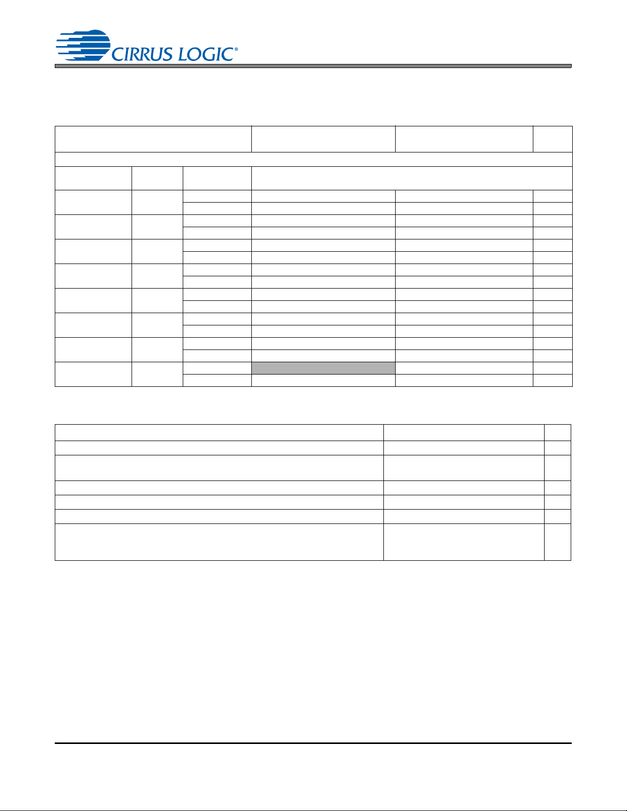
System Features
12, 24, and 27 MHz Master Clock Support in
Addition to Typical Audio Clock Rates
High-performance 24-bit Converters
– Multi-bit Delta-Sigma Architecture
– Very Low 64Fs Oversampling Clock Reduces
Power Consumption
Low-power Operation
– Stereo Analog Passthrough: 10 mW @ 1.8 V
– Stereo Playback: 14 mW @ 1.8 V
– Stereo Rec. and Playback: 23 mW @ 1.8 V
Variable Power Supplies
– 1.8 V to 2.5 V Digital and Analog
– 1.6 V to 5 V Class D Amplifier
– 1.8 V to 2.5 V Headphone Amplifier
– 1.8 V to 3.3 V Interface Logic
Power-down Management
– ADC, DAC, CODEC, MIC Pre-Amplifier, PGA,
Headphone Amplifier, Speaker Amplifier
Analog and Digital Routing/Mixes:
– Line/Headphone Out = Analog In (ADC
Bypassed)
– Line/Headphone/Speaker
Out = ADC + Digital In
– Digital Out = ADC + Digital In
– Internal Digital Loopback
– Mono Mixes
Flexible Clocking Options
– Master or Slave Operation
– High-impedance Digital Output Option (for easy
MUXing between CODEC and other data
sources)
– Quarter-speed Mode - (i.e. allows 8 kHz Fs
while maintaining a flat noise floor up to 16 kHz)
– 4 kHz to 96 kHz Sample Rates
I²C™ Control Port Operation
Headphone/Speaker Detection Input
Pop and Click Suppression
Applications
Digital Voice Recorders, Digital Cameras, and
Camcorders
PDA’s
Personal Media Players
Portable Game Consoles
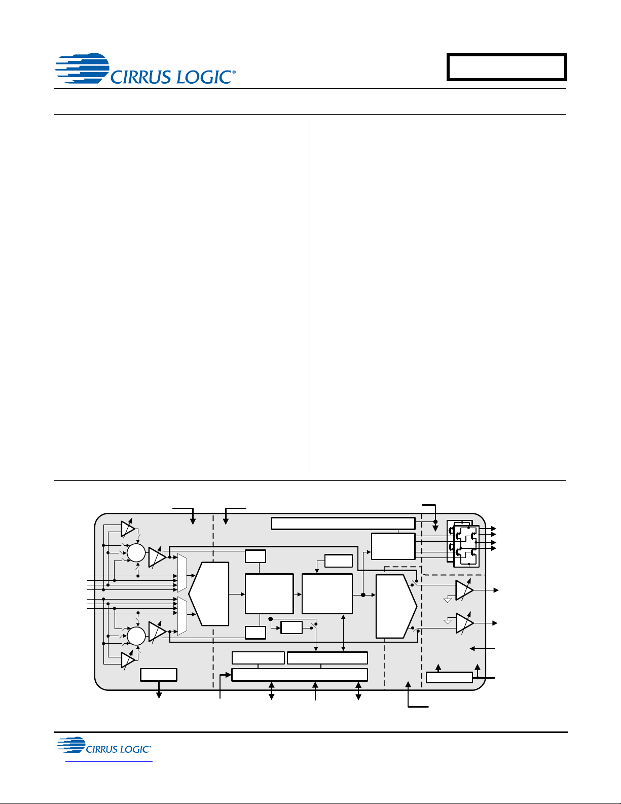
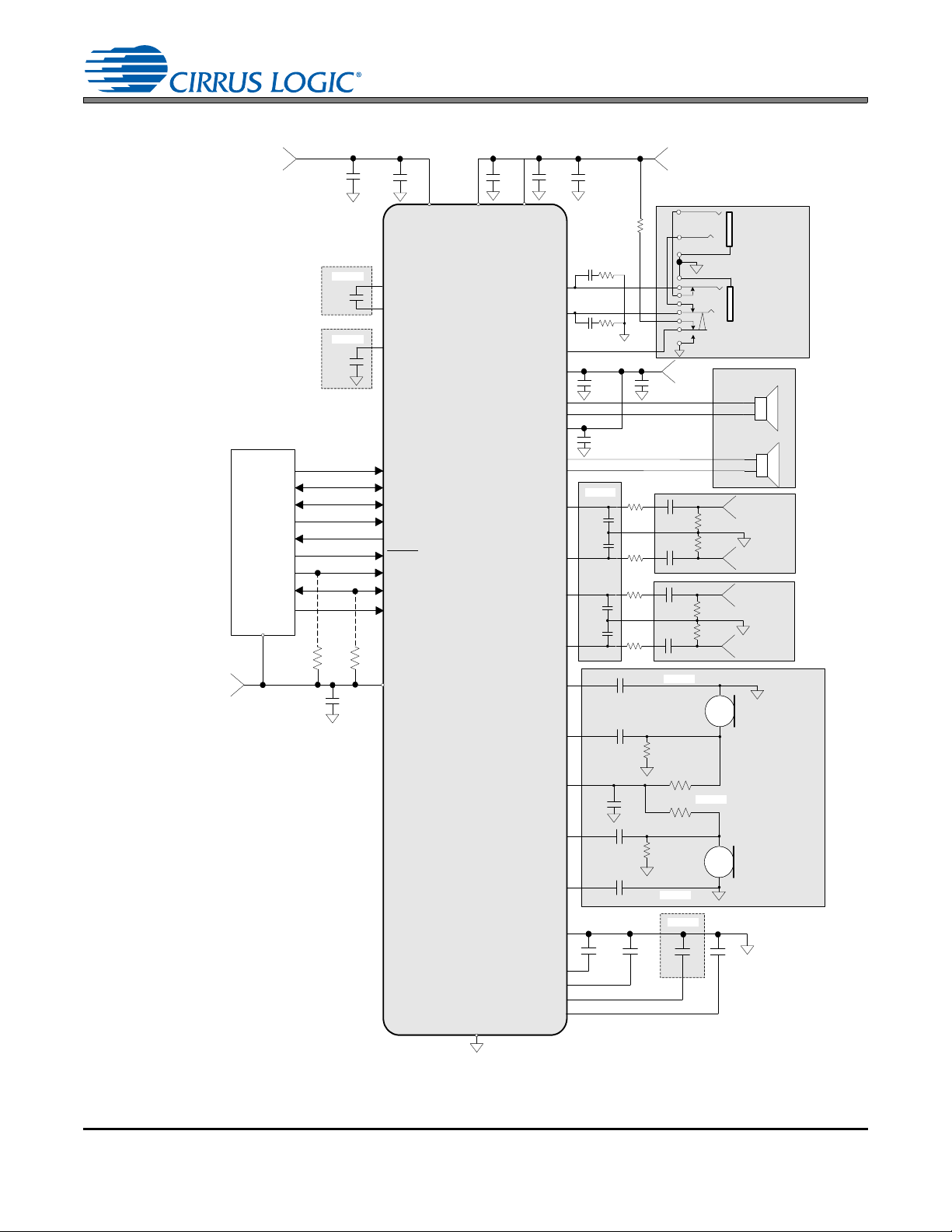
General Description
The CS42L52 is a highly integrated, low-power stereo CODEC with headphone and Class D speaker amplifiers. The
CS42L52 offers many features suitable for low-power, portable system applications.
The ADC input path allows independent channel control of a
number of features. Input summing amplifiers mix and select
line-level and/or microphone-level inputs for each channel.
The microphone input path includes a selectable programmable-gain pre-amplifier stage and a low-noise MIC bias voltage
supply. A PGA is available for line or microphone inputs and
provides analog gain with soft-ramp and zero-cross transitions. The ADC also features a digital volume control with soft
ramp transitions. A programmable ALC and Noise Gate monitor the input signals and adjust the volume levels
appropriately. To conserve power, the ADC may be bypassed
while still allowing full analog volume control.
The DAC output path includes a digital signal processing engine with various fixed-function controls. Tone Control
provides bass and treble adjustment of four selectable corner
frequencies. The Digital Mixer provides independent volume
control for both the ADC output and PCM input signal paths,
as well as a master volume control. Digital Volume controls
may be configured to change on soft-ramp transitions while
the analog controls can be configured to occur on every zero
crossing. The DAC also includes de-emphasis, limiting functions and a BEEP generator, delivering tones selectable
across a range of two full octaves.
The stereo hea dphone amplifier is powered from a separate
positive supply and the integrated charge pump provides a
negative supply. This allows a ground-centered, analog output
with a wide signal swing and eliminates external DC-blocking
capacitors.
The Class D stereo s peaker amplifier does not require an
external filter and provides the high-efficiency amplification required by power-sensitive portable applications. The speaker
amplifier may be powered directly from a battery while the internal DC supply monitoring and compensation provides a
constant gain level as the battery’s voltage decays.
In addition to its many features, the CS42L52 operates from a
low-voltage analog and digital core making it ideal for portable
systems that require extremely low power consumption in a
minimal amount of space.
The CS42L52 is available in a 40-pin QFN package in Commercial (-40 to +85 °C) grade. The CS42L52 Customer
Demonstration board is also available for device evaluation
and implementation suggestions. Refer to “Ordering Informa-
tion” on page 81 for complete ordering information.
2 DS680F2
Page 3

TABLE OF CONTENTS
1. PIN DESCRIPTIONS .............................................................................................................................. 8
1.1 I/O Pin Characteristics ............................. .... ... ... ... .... ... ... ... .... ......................................................... 10
2. TYPICAL CONNECTION DIAGRAM ................................................................................................... 11
3. CHARACTERISTIC AND SPECIFICATIONS ...................................................................................... 12
RECOMMENDED OPERATING CONDITIONS ................................................................................... 12
ABSOLUTE MAXIMUM RATINGS .......................................................................................................12
ANALOG INPUT CHARACTERISTICS ................................................................................................ 13
ADC DIGITAL FILTER CHARACTERISTICS ....................................... ... .... ... ... ... ................................ 14
ANALOG OUTPUT CHARACTERISTICS ............................................................................................ 15
ANALOG PASSTHROUGH CHARACTERISTICS ............................................................................... 16
PWM OUTPUT CHARACTERISTICS ........................ .... ... ... ... .... ... ... ... .......................................... ... ... 17
HEADPHONE OUTPUT POWER CHARACTERISTICS ................................... ... .... ... ... ... ... .... ... ... ... ... 18
LINE OUTPUT VOLTAGE LEVEL CHARACTERISTICS ..................................................................... 19
COMBINED DAC INTERPOLATION AND ONCHIP ANALOG FILTER RESPONSE .......................... 19
SWITCHING SPECIFICATIONS - SERIAL PORT ............................................................................... 20
SWITCHING SPECIFICATIONS - I²C CONTROL PORT ..................................................................... 21
DC ELECTRICAL CHARACTERISTICS .............................................................................................. 22
DIGITAL INTERFACE SPECIFICATIONS AND CHARACTERISTICS ................................................ 22
POWER CONSUMPTION .................................................................................................................... 23
4. APPLICATIONS ................................................................................................................................... 24
4.1 Overview ......................................................................................................................................... 24
4.1.1 Basic Architecture ................................................................................................................. 24
4.1.2 Line and MIC Inputs .............................................................................................................. 24
4.1.3 Line and Headphone Outputs ...............................................................................................24
4.1.4 Speaker Driver Outputs ......................................................................................................... 24
4.1.5 Fixed Function DSP Engine .................................................................................................. 24
4.1.6 Beep Generator ..................................................................................................................... 24
4.1.7 Power Management .............................................................................................................. 24
4.2 Analog Inputs ................................................................................................................................. 25
4.2.1 MIC Inputs ............................................................................................................................. 26
4.2.2 Automatic Level Control (ALC) .............................................................................................. 26
4.2.3 Noise Gate ............................................................................................................................ 27
4.3 Analog Outputs .............................................................................................................................. 28
4.3.1 Beep Generator ..................................................................................................................... 29
4.3.2 Limiter .................................................................................................................................... 30
4.4 Analog In to Analog Out Passthrough ............................................................................................ 31
4.4.1 Overriding the ADC Power Down ... .... ... ... ... .... ... ... ................................................................ 31
4.4.2 Overriding the PGA Power Down ... .... ... ... ... .... ... ... ... .... ... ... ... ... .... ... ... ... .... ... ... ...................... 32
4.5 PWM Outputs ................................................................................................................................. 32
4.5.1 Mono Speaker Output Configuration ..................... .................................... ............................ 32
4.5.2 VP Battery Compensation ........... ... .... ... ... ... .... ... ... ... .... ... ... ... ... .... ... ... ... ................................ 33
4.5.2.1 Maintaining a Desired Output Level ........................................................................... 33
4.6 Serial Port Clocking ........................................................................................................................ 33
4.7 Digital Interface Formats ................................................................................................................ 35
4.7.1 DSP Mode ............................................................................................................................. 35
4.8 Initialization ..................................................................................................................................... 36
4.9 Recommended Power-up Sequence ..............................................................................................37
4.10 Recommended Power-Down Sequence ...................................................................................... 37
4.11 Required Initialization Settings ..................................................................................................... 37
4.12 Control Port Operation .................................................................................................................. 38
4.12.1 I²C Control ................. ... .... .......................................... ... ... ... ... .... ... ...................................... 38
4.12.2 Memory Address Pointer (MAP) .................................... ... ... ... .... ... ... ... .... ... ... ... ... .... ... ... ... ... 39
3/1/13
CS42L52
DS680F2 3
Page 4

3/1/13
CS42L52
4.12.2.1 Map Increment (INCR) ............................................................................................. 39
5. REGISTER QUICK REFERENCE ........................................................................................................ 40
6. REGISTER DESCRIPTION .................................................................................................................. 42
6.1 Chip I.D. and Revision Register (Address 01h) (Read Only) ......................................................... 42
6.1.1 Chip I.D. (Read Only) ............................................................................................................ 42
6.1.2 Chip Revision (Read Only) .................................................................................................... 42
6.2 Power Control 1 (Address 02h) ...................................................................................................... 42
6.2.1 Power Down ADC Charge Pump .......................................................................................... 42
6.2.2 Power Down PGAx ................................................................................................................ 42
6.2.3 Power Down ADCx ................................................................................................................ 43
6.2.4 Power Down ................................................ .......................................... ................................ 43
6.3 Power Control 2 (Address 03h) ...................................................................................................... 43
6.3.1 Power Down ADC Override ................................................................................................... 43
6.3.2 Power Down MICx ................................................................................................................. 43
6.3.3 Power Down MIC Bias .......................................................................................................... 43
6.4 Power Control 3 (Address 04h) ...................................................................................................... 44
6.4.1 Headphone Power Control ....... ... .......................................... ... .... ... ... ... .... ... ......................... 44
6.4.2 Speaker Power Control ............... ... .... ... ... ... .......................................... .... ... ... ...................... 44
6.5 Clocking Control (Address 05h) ...................................................................................................... 44
6.5.1 Auto-Detect ........................ ... ... ... ... .... .......................................... ......................................... 44
6.5.2 Speed Mode ................................................ .......................................... ................................ 45
6.5.3 32kHz Sample Rate Group ................................................................................................... 45
6.5.4 27 MHz Video Clock .............................................................................................................. 45
6.5.5 Internal MCLK/LRCK Ratio ................................................................................................... 45
6.5.6 MCLK Divide By 2 .......... .......................................... .......................................... ................... 46
6.6 Interface Control 1 (Address 06h) .................................................................................................. 46
6.6.1 Master/Slave Mode ............................... ... ............................................................................. 46
6.6.2 SCLK Polarity .................................................. .......................................... ............................ 46
6.6.3 ADC Interface Format ........................... ... ... .... ... ... ... .... ... ... ... ................................................ 46
6.6.4 DSP Mode ................................................... .......................................... ................................ 46
6.6.5 DAC Interface Format ........................... ... ... .... ... ... ... .... ... ... ... ................................................ 47
6.6.6 Audio Word Length ................................................................................................................ 47
6.7 Interface Control 2 (Address 07h) .................................................................................................. 47
6.7.1 SCLK equals MCLK .............................................................................................................. 47
6.7.2 SDOUT to SDIN Digital Loopback ......................................................................................... 47
6.7.3 Tri-State Serial Port Interface ............................. ... ... .... ... ... ... ... ............................................. 48
6.7.4 Speaker/Headphone Switch Invert .................................. ... ... ... .... ... ... ... .... ... ... ... ... .... ............ 48
6.7.5 MIC Bias Level ............... .... ... ... .......................................... ................................................... 48
6.8 Input x Select: ADCA and PGAA (Address 08h), ADCB and PGAB (Address 09h) ....................... 48
6.8.1 ADC Input Select ... ... ... ... .... ................................................................................................... 48
6.8.2 PGA Input Mapping ........ .......................................... .... ... .......................................... ... ......... 49
6.9 Analog and HPF Control (Address 0Ah) ......................................................................................... 49
6.9.1 ADCx High-Pass Filter .......................................................................................................... 49
6.9.2 ADCx High-Pass Filter Freeze ..............................................................................................49
6.9.3 Ch. x Analog Soft Ramp . .... ... .......................................... ... ... ... ............................................. 49
6.9.4 Ch. x Analog Zero Cross .......... .......................................... ... ... ............................................. 49
6.10 ADC HPF Corner Frequency (Address 0Bh) ................................................................................ 50
6.10.1 HPF x Corner Frequency .................................................................................................
6.11 Misc. ADC Control (Address 0Ch) ................................................................................................ 50
6.11.1 Analog Front-End Volume Setting B=A ............................................................................... 50
6.11.2 Digital MUX ......................................................................................................................... 50
6.11.3 Digital Sum .......................................................................................................................... 50
6.11.4 Invert ADC Signal Polarity ................................................................................................... 51
6.11.5 ADC Mute ............................................................................................................................ 51
... 50
4 DS680F2
Page 5

3/1/13
CS42L52
6.12 Playback Control 1 (Address 0Dh) ............................................................................................... 51
6.12.1 Headphone Analog Gain ..................................................................................................... 51
6.12.2 Playback Volume Setting B=A ............................................................................................ 51
6.12.3 Invert PCM Signal Polarity .................................................................................................. 52
6.12.4 Master Playback Mute ......................................................................................................... 52
6.13 Miscellaneous Controls (Address 0Eh) ..................... ... ... .... ... ... ... ... .... ... ... ... .... ... ... ... ... .... ... ... ... ... 52
6.13.1 Passthrough Analog ............... ... .......................................... ... .... ... ... ... .... ... ... ... ... .... ... ......... 52
6.13.2 Passthrough Mute ..................... ... .... ... ... ... .... ... ... ... .... ... .......................................... ... ......... 52
6.13.3 Freeze Registers .... ... ... .... .......................................... ... ... ... ... .... ... ... ................................... 52
6.13.4 HP/Speaker De-emphasis ................................................................................................... 53
6.13.5 Digital Soft Ramp ................................................................................................................ 53
6.13.6 Digital Zero Cross ................................... ... .... ... ... ... .... ... .......................................... ............ 53
6.14 Playback Control 2 (Address 0Fh) ................................................................................................ 54
6.14.1 Headphone Mute ....... ... .... ... ... .......................................... ... ... .... ... ... ... .... ... ... ... ... .... ... ......... 54
6.14.2 Speaker Mute ................... ... ... .......................................... ... ... .... ... ... ... ................................ 54
6.14.3 Speaker Volume Setting B=A ..............................................................................................54
6.14.4 Speaker Channel Swap ....................................................................................................... 54
6.14.5 Speaker MONO Control ...................................................................................................... 54
6.14.6 Speaker Mute 50/50 Control ............................................................................................... 54
6.15 MICx Amp Control:MIC A (Address 10h) and MIC B (Address 11h) ............................................ 55
6.15.1 MIC x Select ........................................................................................................................ 55
6.15.2 MICx Configuration .............................. ... ... .... ... ... ... .... ... .......................................... ............ 55
6.15.3 MICx Gain ................................. ... .... ... ... ... .......................................... .... ... ... ...................... 55
6.16 PGAx Vol. and ALCx Transition Ctl.:
ALC, PGA A (Address 12h) and ALC, PGA B (Address 13h) .............................................................. 55
6.16.1 ALCx Soft Ramp Disable ..................................................................................................... 55
6.16.2 ALCx Zero Cross Disable .................................................................................................... 56
6.16.3 PGAx Volume .. .... ... ... ... .... ... ... ... ... .......................................... .... ... ... ... .... ... ... ...................... 56
6.17 Passthrough x Volume: PASSAVOL (Address 14h) and PASSBVOL (Address 15h) ................. 57
6.17.1 Passthrough x Volume ........................................................................................................ 57
6.18 ADCx Volume Control: ADCAVOL (Address 16h) and ADCBVOL (Address 17h) ....................... 57
6.18.1 ADCx Volume ...... .......................................... ... ... ... .... ... ... ... ................................................ 57
6.19 ADCx Mixer Volume: ADCA (Address 18h) and ADCB (Address 19h) ........................................ 58
6.19.1 ADC Mixer Channel x Mute ................................................................................................. 58
6.19.2 ADC Mixer Channel x Volume ............................................................................................. 58
6.20 PCMx Mixer Volume: PCMA (Address 1Ah) and PCMB (Address 1Bh) ...................................... 58
6.20.1 PCM Mixer Channel x Mute ................................................................................................58
6.20.2 PCM Mixer Channel x Volume ............................................................................................ 58
6.21 Beep Frequency and On Time (Address 1Ch) ............................................................................. 59
6.21.1 Beep Frequency ..................................................... .... ... ... ... ... .... ... ...................................... 59
6.21.2 Beep On Time ..................... ... ... ... .... ... ... ... .... ... ... ... .... ......................................... .... ............ 60
6.22 Beep Volume and Off Time (Address 1Dh) .................................................................................. 60
6.22.1 Beep Off Time ..................... ... ... ... .... ... ... ... .... .......................................... ... ... ... ... .... ............ 60
6.22.2 Beep Volume .......... ... ... .... ... .......................................... ... ... ... .... ... ... ... .... ... ... ... ... .... ............ 61
6.23 Beep and Tone Configuration (Address 1Eh) ............................................................................... 61
6.23.1 Beep Configuration ........................................... ... ... .... ... ... ... ................................................ 61
6.23.2 Beep Mix Disable ................................................................................................................ 61
6.23.3 Treble Corner Frequency ................. ... ... ... .... ... ... ... .... ... ... ... ... .... ... ... ... .... ... ... ... ................... 62
6.23.4 Bass Corner Frequency ......................... ... .... ... ... ... .......................................... ... .... ... ... ...... 62
6.23.5 Tone Control Enable .............................. ... .... ... ... ... .... ... ... ... ................................................ 62
6.24 Tone Control (Address 1Fh) ............................................ .... ... ... ... ... .... ... ... ... .... ... ... ... ................... 62
6.24.1 Treble Gain ............................................................................. .... ... ... ... .... ... ......................... 62
6.24.2 Bass Gain ......................................... .......................................... ......................................... 63
6.25 Master Volume Control: MSTA (Address 20h) and MSTB (Address 21h) .................................... 63
DS680F2 5
Page 6

3/1/13
CS42L52
6.25.1 Master Volume Control ........................................................................................................ 63
6.26 Headphone Volume Control: HPA (Address 22h) and HPB (Address 23h) ................................. 63
6.26.1 Headphone Volume Control ................... ................................................................. ............63
6.27 Speaker Volume Control: SPKA (Address 24h) and SPKB (Address 25h) .................................. 64
6.27.1 Speaker Volume Control ..................................................................................................... 64
6.28 ADC and PCM Channel Mixer (Address 26h) ................................. .... ... ... ... .... ... ... ... ... .... ... ... ... ... 64
6.28.1 PCM Mix Channel Swap .....................................................................................................64
6.28.2 ADC Mix Channel Swap ...................................................................................................... 64
6.29 Limiter Control 1, Min/Max Thresholds (Address 27h) ................................................................. 65
6.29.1 Limiter Maximum Threshold ............................. ................................................................... 65
6.29.2 Limiter Cushion Threshold .................................................................................................. 65
6.29.3 Limiter Soft Ramp Disable ......................... ....... ...... ....... ...... ....... ...... ....... ...... ...... ....... ......... 65
6.29.4 Limiter Zero Cross Disable ..................... .................................... ................................... ...... 66
6.30 Limiter Control 2, Release Rate (Address 28h) ......................... ............................................. ......66
6.30.1 Peak Detect and Limiter ...................................................................................................... 66
6.30.2 Peak Signal Limit All Channels ........................................................................................... 66
6.30.3 Limiter Release Rate ...........................................................................................................66
6.31 Limiter Attack Rate (Address 29h) ................................................................................................ 67
6.31.1 Limiter Attack Rate .............................................................................................................. 67
6.32 ALC Enable and Attack Rate (Address 2Ah) ................ ... .... ... ... ... ... .......................................... ... 67
6.32.1 ALCx Enable ....................................................................................................................... 67
6.32.2 ALC Attack Rate .................................................................................................................. 67
6.33 ALC Release Rate (Address 2Bh) ...................... .......................................... ................................ 68
6.33.1 ALC Release Rate ............................................................................................................... 68
6.34 ALC Threshold (Address 2Ch) ..................................................................................................... 68
6.34.1 ALC Maximum Threshold .................................................................................................... 68
6.34.2 ALC Minimum Threshold ..................................................................................................... 69
6.35 Noise Gate Control (Address 2Dh) ......................... ... ................................................................... 69
6.35.1 Noise Gate All Channels ..................................................................................................... 69
6.35.2 Noise Gate Enable .............................................................................................................. 69
6.35.3 Noise Gate Threshold and Boost ........................................................................................ 70
6.35.4 Noise Gate Delay Timing ....................................................................................................70
6.36 Status (Address 2Eh) (Read Only) ..... ... .... .......................................... ... ... ... .... ... ... ... ... .... ... ... ...... 70
6.36.1 Serial Port Clock Error (Read Only) ....................................................................................70
6.36.2 DSP Engine Overflow (Read Only) ..................................................................................... 71
6.36.3 PCMx Overflow (Read Only) ...............................................................................................71
6.36.4 ADCx Overflow (Read Only) ...............................................................................................71
6.37 Battery Compensation (Address 2Fh) .......................................................................................... 71
6.37.1 Battery Compensation ......................... ................................... .................................... ......... 71
6.37.2 VP Monitor .................................... .... ... ... ... .... .......................................... ... ... ... ................... 71
6.37.3 VP Reference ...................................................................................................................... 72
6.38 VP Battery Level (Address 30h) (Read Only) ............................................................................... 72
6.38.1 VP Voltage Level (Read Only) ............................................................................................72
6.39 Speaker Status (Address 31h) (Read Only) ..................................................................... ... ... ... ... 72
6.39.1 Speaker Current Load Status (Read Only) ......................................................................... 72
6.39.2 SPKR/HP Pin Status (Read Only) ....................................................................................... 73
6.40 Charge Pump Frequency (Address 34h) ...................................................................................... 73
6.40.1 Charge Pump Frequency .................................................................................................... 73
7. ANALOG PERFORMANCE PLOTS .......... ... .... ... ... .......................................... ... .... ... ... ... ... .... ... ... ... ...74
7.1 Headphone THD+N versus Output Power Plots ............................................................................ 74
8. EXAMPLE SYSTEM CLOCK FREQUENCIES .................................................................................... 76
8.1 Auto Detect Enabled .................................................................................................................... 76
8.2 Auto Detect Disabled .................................................................................................................... 76
9. PCB LAYOUT CONSIDERATIONS ..................................................................................................... 77
6 DS680F2
Page 7

9.1 Power Supply and Grounding ......................................................................................................... 77
9.2 QFN Thermal Pad .......................................................................................................................... 77
10. ADC AND DAC DIGITAL FILTERS .................................................. ... .... ... ... ... .... ............................ 78
11. PARAMETER DEFINITIONS .............. ... ... ... .... ... ... ... .... ... .......................................... ... ... ... .... ............ 79
12. PACKAGE DIMENSIONS ........... .... ... ... ... ... .......................................... .... ... ... ................................... 80
THERMAL CHARACTERISTICS ....... ... ... ... ... .... ... ... ... .... ... ... ... .... ... .......................................... ... ... ...... 80
13. ORDERING INFORMATION ....... .... ... ... ... ... .... ... ... ... .... .......................................... ... ... ... ... .... ... ......... 81
14. REFERENCES ....................... ... ... .... ... ... ... ... .... ... ... .......................................... ... .... ............................ 81
15. REVISION HISTORY ................................ ... .... ... .......................................... ... ... ................................ 81
LIST OF TABLES
Table 1. MCLK, LRCK Quick Decode ....................................................................................................... 34
LIST OF FIGURES
Figure 1. Typical Connection Diagram ...................................................................................................... 11
Figure 2. Headphone Output Test Load .................................................................................................... 18
Figure 3. Serial Audio Interface Timing ..................................................................................................... 20
Figure 4. Control Port Timing - I²C ............................................................................................................ 21
Figure 5. Analog Input Signal Flow ........................................................................................................... 25
Figure 6. Single-Ended MIC Configuration ............................................................................................... 26
Figure 7. Differential MIC Configuration .................................................................................................... 26
Figure 8. ALC ............................................................................................................................................ 27
Figure 9. Noise Gate Attenuation .............................................................................................................. 27
Figure 10. DSP Engine Signal Flow .......................................................................................................... 28
Figure 11. PWM Output Stage .................................................................................................................. 29
Figure 12. Analog Output Stage ................................................................................................................ 29
Figure 13. Beep Configuration Options ..................................................................................................... 30
Figure 14. Peak Detect and Limiter ........................................................................................................... 31
Figure 15. Battery Compensation ............................................................................................................. 33
Figure 16. I²S Format ................................................................................................................................ 35
Figure 17. Left-Justified Format ................................................................................................................ 35
Figure 18. Right-Justified Format (DAC only) ........................................................................................... 35
Figure 19. DSP Mode Format) .................................................................................................................. 36
Figure 20. Control Port Timing, I²C Write .................................................................................................. 38
Figure 21. Control Port Timing, I²C Read .................................................................................................. 39
Figure 22. THD+N vs. Output Power per Channel at 1.8 V (16 load) .......................... ... ...................... 74
Figure 23. THD+N vs. Output Power per Channel at 2.5 V (16 load) .......................... ... ...................... 74
Figure 24. THD+N vs. Output Power per Channel at 1.8 V (32 load) .......................... ... ...................... 75
Figure 25. THD+N vs. Output Power per Channel at 2.5 V (32 load) .......................... ... ...................... 75
Figure 26. ADC Passband Ripple ............................................................................................................. 78
Figure 27. ADC Stopband Rejection ......................................................................................................... 78
Figure 28. ADC Transition Band ............................................................................................................... 78
Figure 29. ADC Transition Band (Detail) ................................................................................................... 78
Figure 30. DAC Passband Ripple ............................................................................................................. 78
Figure 31. DAC Stopband ......................................................................................................................... 78
Figure 32. DAC Transition Band ............................................................................................................... 78
Figure 33. DAC Transition Band (Detail) ................................................................................................... 78
3/1/13
CS42L52
DS680F2 7
Page 8
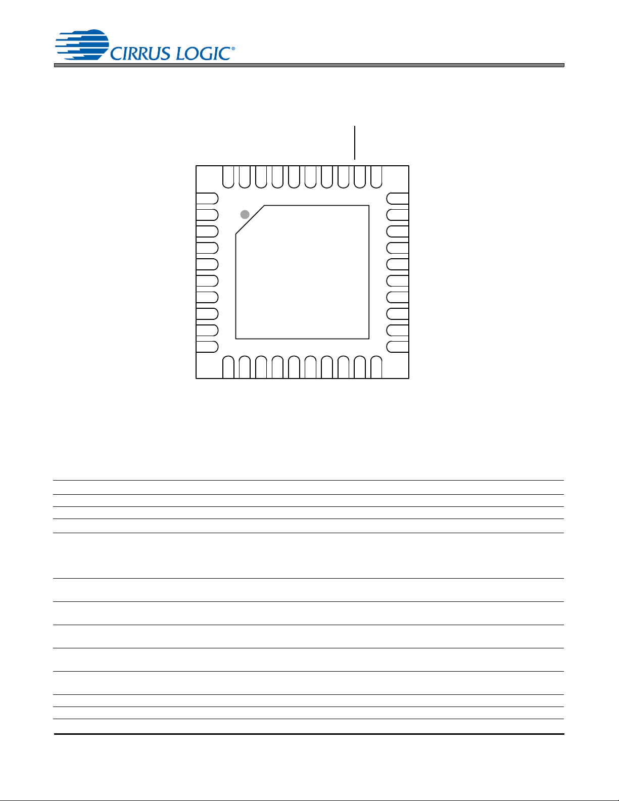
1. PIN DESCRIPTIONS
12
11
13
14
15
16
17
18
19
20
29
30
28
27
26
25
24
23
22
21
39
40
38
37
36
35
34
33
32
31
2
1
3
4
5
6
7
8
9
10
GND/Thermal Pad
SDOUT
MCLK
SCLK
SDIN
SDA
LRCK
FLYN
+VHP
HP/LINE_OUTB
HP/LINE_OUTA
VQ
MICBIAS
AIN4A/MIC1+/MIC2A
AIN2A
AD0
SPKR_OUTA+
VP
VP
VD
SPKR_OUTB-
-VHPFILT
AIN4B/MIC2+/MIC2B
AIN1B
AIN2B
AFILTB
AIN3B/MIC2-/MIC1B
AFILTA
AIN1A
AIN3A/MIC1-/MIC1A
SPKR_OUTB+
SCL
DGND
SPKR_OUTA-
FLYP
VA
AGND
FILT+
RESET
VL
SPKR/HP
Top-Down (Through-Package) View
40-Pin QFN Package
3/1/13
CS42L52
Pin Name # Pin Description
SDA 1 Serial Control Data (Input/Output) - SDA is a data I/O in I²C Mode.
SCL 2 Serial Control Port Clock (Input) - Serial clock for the serial control port.
AD0 3
SPKR_OUTA+
SPKR_OUTASPKR_OUTB+
SPKR_OUTB-
VP
-VHPFILT 10
FLYN 11
FLYP 12
+VHP 13
HP/LINE_OUTB, A 14,15 Headphone/Line Audio Output (Output) - Stereo headphone or line level analog outputs.
VA 16 Analog Power (Input) - Positive power for the internal analog section.
8 DS680F2
Address Bit 0 (Input) - Chip address bit 0.
4
6
PWM Speaker Output (Output) - Full-bridge amplified PWM speaker outputs.
7
9
5
Power for PWM Drivers (Input) - Power supply for the PWM output driver stages.
8
Inverting Charge Pump Filter Connection (Output) - Power supply from the inverting charge
pump that provides the negative rail for the headphone/line amplifi e rs.
Charge Pump Cap Negative Node (Output) - Negative node for the inverting charge pump’s fly-
ing capacitor.
Charge Pump Cap Positive Node (Output) - Positive node for the inverting charge pump’s flying
capacitor.
Positive Analog Power for Headphone (Input) - Positive voltage rail and power for the internal
headphone amplifiers and inverting charge pump.
Page 9
3/1/13
CS42L52
AGND 17 Analog Ground (Input) - Ground reference for the internal analog section.
FILT+ 18
VQ 19 Quiescent Voltage (Output) - Filter connection for the internal quiescent voltage.
MICBIAS 20
AIN4A,B
AIN3A,B
MIC1+,MIC2+,MIC2A,B
MIC1A,B
AIN2A,B
AIN1A,B
AFILTA,B 27,28 Anti-alias Filter Connection (Output) - Anti-alias filter connection for the ADC inputs.
SPKR/HP 31
RESET
VL 33
VD 34 Digital Power (Input) - Positive power for the internal digital section.
DGND 35 Digital Ground (Input) - Ground reference for the internal digital section.
SDOUT 36 Serial Audio Data Output (Output) - Output for two’s complement serial audio data.
MCLK 37 Master Clock (Input) - Clock source for the delta-sigma modulators.
SCLK 38 Serial Clock (Input/Output) - Serial clock for the serial audio interface.
SDIN 39 Serial Audio Data Input (Input) - Input for two’s complement serial audio data.
LRCK 40
GND/Thermal Pad -
Positive Voltage Reference (Output) - Positive reference voltage for the internal sampling cir-
cuits.
Microphone Bias (Output) - Low noise bias supply for an external microphone. Electrical characteristics are specified in the DC Electrical Characteristics table.
21,22
Line-Level Analog Inputs (Input) - Single-ended stereo line-level analog inputs.
23,24
21,23
Differential Microphone Inputs (Input) - Differential stereo microphone inputs.
22,24
21,22
Single-Ended Microphone Inputs (Input) - Single-ended stereo microphone inputs.
23,24
25,26
Line-Level Analog Inputs (Input) - Single-ended stereo line-level analog inputs.
29,30
Speaker/Headphone Switch (Input) - Powers down the left and/or right channel of the speaker
and/or headphone outputs.
32 Reset (Input) - The device enters a low power mode when this pin is driven low.
Digital Interface Power (Input) - Determines the required signal level for the serial audio interface and host control port.
Left Right Clock (Input/Output) - Determines which channel, Left or Right, is currently active on
the serial audio data line.
Ground reference for PWM power FETs and charge pump; thermal relief pad for optimized heat
dissipation.
DS680F2 9
Page 10
1.1 I/O Pin Characteristics
Input and output levels and associated power supply voltage are shown in the table below. Logic levels
should not exceed the corresponding power supply voltage.
3/1/13
CS42L52
Power
Supply
VL
VA SPKR/HP Input - - 1.65 V - 2.63 V
VP
Pin Name I/O Internal
Driver Receiver
Connections
RESET Input - - 1.65 V - 3.47 V, with Hysteresis
AD0 Input - - 1.65 V - 3.47 V, with Hysteresis
SCL Input - - 1.65 V - 3.47 V, with Hysteresis
SDA Input/
Output
MCLK Input - - 1.65 V - 3.47 V
LRCK Input/
Output
SCLK Input/
Output
SDOUT Output Weak Pullup
SDIN Input - - 1.65 V - 3.47 V
SPKR_OUTA+ Output - 1.6 V - 5.25 V Power MOSFET -
SPKR_OUTA- Output - 1.6 V - 5.25 V Power MOSFET -
SPKR_OUTB+ Output - 1.6 V - 5.25 V Power MOSFET -
SPKR_OUTB- Output - 1.6 V - 5.25 V Power MOSFET -
- 1.65 V - 3.47 V, CMOS/Open
Drain
Weak Pullup
(~1 M)
Weak Pullup
(~1 M)
(~1 M)
1.65 V - 3.47 V, CMOS 1.65 V - 3.47 V
1.65 V - 3.47 V, CMOS 1.65 V - 3.47 V
1.65 V - 3.47 V, CMOS
1.65 V - 3.47 V, with Hysteresis
10 DS680F2
Page 11
2. TYPICAL CONNECTION DIAGRAM
Note 4
Note 3
Note 2
Note 1
1 µF
+1.8 V to +2.5 V
0.1 µF
1 µF
DGND
VL
0.1 µF
+1.8 V to + 3 .3 V
SCL
SDA
RESET
2 k
LRCK
Digital Audio
Processor
MCLK
SCLK
VD
MIC1-
AIN3A/MIC1A
Microphone 1
SDIN
SDOUT
CS42L52
2 k
MICBIAS
+1.8 V to + 2 .5 V
HP/LIN E_OUTB
HP/LINE_OUTA
AIN1A
Left 1
1800 pF
1800 pF
100 k
100
AIN1B
Right 1
*
*
R
L
0.1 µF
VA
Headphone Out
Left & Right
Line Level Out
Left & Right
FLYP
FLYN
-VHPFILT
0.1 µF
51.1
0.022 µF
100 k
100
SPKR_OUTA+
SPKR_OUTA-
SPKR/HP
51.1
0.022 µF
MIC1+
AIN4A/MIC2A
MIC2+
AIN4B/MIC2B
Microphone 2
MIC2-
AIN3B/MIC1B
100 k
R
L
100 k
1 µF
1 µF
0.1 µF
+VHP
1 µF
10 µF
VQ
AGND
* Capacitors must be C0G or equivalent
150 pF
AFILTA
AFILTB
150 pF
1 µF
**
FILT+
1 µF
1 µF
1 µF
1 µF
* *Use low ESR ceramic capacitors.
**
**
See Note 5
SPKR_OUTB+
SPKR_OUTB-
1 µF
VP
VP
+1.6 V to
+5 V
Stereo Speakers
AIN2A
Left 2
1800 pF
1800 pF
100 k
100
AIN2B
Right 2
*
*
100 k
100
1 µF
1 µF
0.1 µF
0.1 µF
Analog
Input 1
Analog
Input 2
10 µF
Mic-Level
Inputs
47 k
Notes:
1. Recommended values for the default charge pump switching
frequency. The required capacitance follows an inverse
relationship with the charge pump’s switching frequency. When
increasing the switching frequency, the capacitance may
decrease; when lowering the switching frequency, the
capacitance must increase.
2. Larger capacitance reduces the ripple on the internal
amplifier’s supply. This may reduce the distortion at higher
output power levels.
3. Additional bulk capacitance may be added to improve PSRR
at low frequencies.
4. These capacitors serve as a charge reservoir for the internal
switched capacitor ADC modulators. They are only needed
when the PGA (Programmable Gain Amplifier) is bypassed.
5. Series resistance in the path of the power supplies must be
avoided. Any voltage drop on VHP will dire c tly impact the
negative charge pump supply (-VHPFILT) and clip the audio
output.
6. The value of R
L
, a current-limiting resistor used with electret
condenser microphones, is dictated by the microphone
cartridge.
7. The negative terminal of the MICx inputs connects to the
ground pin of the microphone cartridge. Gain is applied only to
the positive te rminal.
Note 6
Note 7
Note 7
AD0
Figure 1. Typical Connection Diagram
3/1/13
CS42L52
DS680F2 11
Page 12
3/1/13
CS42L52
3. CHARACTERISTIC AND SPECIFICATIONS
RECOMMENDED OPERATING CONDITIONS
AGND=DGND=0 V, All voltages with respect to ground.
Parameters Symbol Min Max Units
DC Power Supply
Analog VA 1.65 2.63 V
Headphone Amplifier +VHP 1.65 2.63 V
Speaker Amplifier VP 1.60 5.25 V
Digital VD 1.65 2.63 V
Serial/Control Port Interface VL 1.65 3.47 V
Ambient Temperature Commercial - CNZ T
A
-40 +85 C
ABSOLUTE MAXIMUM RATINGS
AGND = DGND = 0 V; All voltages with respect to ground.
Parameters Symbol Min Max Units
DC Power Supply Analog
Speaker
Digital
Serial/Control Port Interface
Input Current (Note 1) I
External Voltage Applied to Analog Input (Note 2)
External Voltage Applied to Analog Output
External Voltage Applied to Digital Input (Note 2) V
Ambient Operating Temperature (power applied) T
Storage Temperature T
WARNING:Operation at or beyond these limits may result in permanent damage to the device. Normal operation
is not guaranteed at these extremes.
VA, VHP
VP
VD
VL
in
V
IN
V
IN
IND
A
stg
-0.3
-0.3
-0.3
-0.3
-±10mA
AGND-0.3 VA+0.3
-VHP - 0.3 +VHP + 0.3
-0.3 VL+ 0.3 V
-50 +115 °C
-65 +150 °C
3.0
6.0
3.0
4.0
V
V
V
V
V
V
Notes:
1. Any pin except supplies. Transient currents of up to ±100 mA on the analog input pins will not cause
SCR latch-up.
2. The maximum over/under voltage is limited by the input current.
12 DS680F2
Page 13
3/1/13
CS42L52
ANALOG INPUT CHARACTERISTICS
Test Conditions (unless otherwise specified): Input sine wave (relative to digital full scale): 1 kHz through passive input filter; All
Supplies = VA; T
fied; “Required Initialization Settings” on page 37 written on power up.
Analog In to ADC (PGA bypassed)
Dynamic Range A-weighted
Total Harmonic Distortion + Noise -1 dBFS
Analog In to PGA to ADC
Dynamic Range
PGA Setting: 0 dB A-weighted
PGA Setting: +12 dB A-weighted
Total Harmonic Distortion + Noise
PGA Setting: 0 dB -1 dBFS
-60 dBFS
PGA Setting: +12 dB -1 dBFS - -85 -79 - -83 -77 dB
Analog In to MIC Pre-Amp (+16 dB) to PGA to ADC
Dynamic Range
PGA Setting: 0 dB A-weighted
Total Harmonic Distortion + Noise
PGA Setting: 0 dB -1 dBFS - -76 - - -74 - dB
Analog In to MIC Pre-Amp (+32 dB) to PGA to ADC
Dynamic Range
PGA Setting: 0 dB A-weighted
Total Harmonic Distortion + Noise
PGA Setting: 0 dB -2 dBFS - -74 - - -71 - dB
Other Characteristics
DC Accuracy
Interchannel Gain Mismatch - 0.2 - - 0.2 - dB
Gain Drift - ±100 - - ±100 - p pm/°C
Offset Error SDOUT Code with HPF On - 352 - - 352 - LSB
Input
Interchannel Isolation - 90 - - 90 - dB
HP Amp to Analog Input Isolation R
(Note 3) R
Speaker Amp to Analog Input Isolation - 60 - - 60 - dB
Full-scale Input Voltage ADC
Input Impedance (Note 4) ADC
3. Measured with DAC delivering full-scale output into specified load.
4. Measured between analog input and AGND.
= +25C; Sample Frequency = 48 kHz; Measurement Bandwidth is 20 Hz to 20 kHz unless otherwise speci-
A
VA = 2.5V VA = 1.8V
Parameters Min Typ Max Min Typ Max Unit
unweighted9390
-20 dBFS
-60 dBFS
unweighted9289
unweighted8582
unweighted
unweighted
= 10 k
L
= 16
L
PGA (0 dB)
PGA (+12 dB)
MIC (+16 dB)
MIC (+32 dB)
PGA
MIC
-
-
-
-
-
-
-
-
-
-
-
0.73•VA
0.73•VA
-
-
-
99
96
-86
-76
-36
96
93
91
88
-88
-33
86
83
76
73
100
70
0.769•VA
0.770•VA
0.194•VA
0.115•VA
0.019•VA
20
39
50
-
-
-80
-
-30
-
-
-
-
-82
-27
-
-
-
-
-
-
0.83•VA
0.83•VA
-
-
-
90
87
-
-
-
89
86
82
79
-
-
-
-
-
-
-
-
0.73•VA
0.73•VA
-
-
-
96
93
-84
-73
-33
95
92
88
85
-86
-32
83
80
74
71
100
70
0.769•VA
0.770•VA
0.194•VA
0.1 15•VA
0.019•VA
20
39
50
-
-
-78
-
-27
-
-
-
-
-80
-26
-
-
-
-
-
-
0.83•VA
0.83•VA
-
-
-
dB
dB
dB
dB
dB
dB
dB
dB
dB
dB
dB
dB
dB
dB
dB
dB
dB
Vpp
Vpp
Vpp
Vpp
Vpp
k
k
k
DS680F2 13
Page 14
3/1/13
CS42L52
ADC DIGITAL FILTER CHARACTERISTICS
Parameters (Note 5) Min Typ Max Unit
Passband (Frequency Response) to -0.1 dB corner 0 - 0.4948 Fs
Passband Ripple -0.09 - 0.17 dB
Stopband 0.6 - - Fs
Stopband Attenuation 33 - - dB
Total Group Delay -7.6/Fs- s
High-Pass Filter Characteristics (48 kHz Fs)
Frequency Response -3.0 dB
-0.13 dB
Phase Deviation @ 20 Hz - 10 - Deg
Passband Ripple - - 0.17 dB
Filter Settling Time -10
5. Response is clock-dependent and will scale with Fs. Note that the response plots (Figures 26 to 29 on
page 78) have been normalized to Fs and can be de-normalized by multiplying the X-axis scale by Fs.
HPF parameters are for Fs = 48 kHz.
-
-
3.6
24.2
5
/Fs 0 s
-
-
Hz
Hz
14 DS680F2
Page 15
3/1/13
CS42L52
ANALOG OUTPUT CHARACTERISTICS
Test conditions (unless otherwise specified): Input test signal is a full-scale 997 Hz sine wave; All Supplies = VA; TA = +25C;
Sample Frequency = 48 kHz; Measurement bandwidth is 20 Hz to 20 kHz; Test load R
(see Figure 2); Test load RL = 16 CL = 10 pF (see Figure 2) for the headphone output; HP_GAIN[2:0] = 011; “Required Initial-
ization Settings” on page 37 written on power up.
VA = 2.5 V VA = 1.8 V
Parameters
R
= 10 k
L
Dynamic Range
18- to 24-Bit A-weighted
unweighted
16-Bit A-weighted
Total Harmonic Distortion + Noise
18- to 24-Bit 0 dB
16-Bit 0 dB
RL = 16
Dynamic Range
18- to 24-Bit A-weighted
16-Bit A-weighted
Total Harmonic Distortion + Noise
18- to 24-Bit 0 dB
16-Bit 0 dB
Other Characteristics for R
Output Parameters Modulation Index (MI)
(Note 7) Analog Gain Multiplier (G)
Full-scale Output Voltage (2•G•MI•VA) (Note 7) See “Line Output Voltage Level Characteristics” on
Full-scale Output Power (Note 7) See “Headphone Output Power Characteristics” on page 18
Interchannel Isolation (1 kHz) 16
Speaker Amp to HP Amp Isolation - 80 - - 80 - dB
Interchannel Gain Mismatch - 0.1 0.25 - 0.1 0.25 dB
Gain Drift - ±100 - - ±100 - ppm/°C
AC Load Resistance (R
Load Capacitance (C
L
) (Note 8) - - 150 - - 150 pF
L
(Note 6) Min Typ Max Min Typ Max Unit
92
89
-
unweighted
-20 dB
-60 dB
-20 dB
-60 dB
unweighted
unweighted
-20 dB
-60 dB
-20 dB
-60 dB
= 16 or 10 k
L
) (Note 8) 16 - - 16 - -
10 k
-
-
-
-
-
-
-
92
89
-
-
-
-
-
-
-
-
-
-
page 19
-
-
98
95
96
93
-86
-75
-35
-86
-73
-33
98
95
96
93
-75
-75
-35
-75
-73
-33
0.6787
0.6047
80
95
= 10 k CL = 10 pFfor the line output
L
-
-
-
-
-80
-
-29
-
-
-
-
-
-
-
-69
-
-29
-
-
-
-
-
-
-
89
86
89
86
95
92
-
-
-
-
-
-
-
-
-
-
-
-
-
-
-
-
-
-
-
-
93
90
-88
-72
-32
-88
-70
-30
95
92
93
90
-75
-72
-32
-75
-70
-30
0.6787
0.6047
80
93
-
-
-
-
-82
-
-26
-
-
-
-
-
-
-
-69
-
-26
-
-
-
-
-
-
-
dB
dB
dB
dB
dB
dB
dB
dB
dB
dB
dB
dB
dB
dB
dB
dB
dB
dB
dB
dB
Vpp
dB
dB
6. One (least-significant bit) LSB of triangular PDF dither is added to data.
7. Full-scale output voltage and power is determined by the gain setting, G, in register “Headphone Analog
Gain” on page 51. High gain settings at certain VA and VHP supply levels may cause clipping when the
audio signal approaches full-scale, maximum power output, as shown in Figures 22 - 25 on page 75.
DS680F2 15
Page 16
3/1/13
CS42L52
8. See Figure 2. RL and CL reflect the recommended minimum resistance and maximum capacitance required for the internal op-amp's stability and signal integrity. In this circuit topology, C
will effectively
L
move the band-limiting pole of the amp in the output stage. Increasing this value beyond the recommended 150 pF can cause the internal op-amp to become unstable.
ANALOG PASSTHROUGH CHARACTERISTICS
Test Conditions (unless otherwise specified): Input sine wave (relative to full-scale): 1 kHz through passive input filter; PGA and
HP/Line Gain = 0 dB; All Supplies = VA; T
“Required Initialization Settings” on page 37 written on power up.
Parameters Min Typ Max Min Typ Max Unit
Analog In to HP/Line Amp (ADC is powered down)
R
= 10 k
= 16
L
Dynamic Range A-weig hted
Total Harmonic Distortion + Noise -1 dBFS
-20 dBFS
Full-scale Input Voltage - 0.91•VA - - 0.91•VA - Vpp
Full-scale Output Voltage - 0.84•VA - - 0.84•VA - Vpp
Passband Ripple - 0/-0.3 - - 0/-0.3 - dB
R
L
Dynamic Range A-weig hted
Total Harmonic Distortion + Noise -1 dBFS
-20 dBFS
Full-scale Input Voltage - 0.91•VA - - 0.91•VA - Vpp
Full-scale Output Voltage - 0.84•VA - - 0.84•VA - Vpp
Output Power - 32 - - 17 - mW
Passband Ripple - 0/-0.3 - - 0/-0.3 - dB
= +25C; Sample Frequency = 48 kHz; Measurement Bandwidth is 20 Hz to 20 kHz;
A
VA = 2.5 V VA = 1.8 V
unweighted
-60 dBFS
unweighted
-60 dBFS
-
-
-
-
-
-
-
-
-
-
-96
-93
-70
-73
-33
-96
-93
-70
-73
-33
-
-
-
-
-
-
-
-
-
-
-
-
-
-
-
-
-
-
-
-
-94
-91
-70
-71
-31
-94
-91
-70
-71
-31
-
-
-
-
-
-
-
-
-
-
dB
dB
dB
dB
dB
dB
dB
dB
dB
dB
16 DS680F2
Page 17
3/1/13
CS42L52
PWM OUTPUT CHARACTERISTICS
Test conditions (unless otherwise specified): Input test signal is a full scale 997 Hz signal; MCLK = 12.2880 MHz; Measurement
Bandwidth is 20 Hz to 20 kHz; Sample Frequency = 48 kHz; Test load R
full-bridge; VD = VL = VA = VHP = 1.8 V; PWM Modulation Index of 0.85; PWM Switch Rate = 384 kHz; “Required Initialization
Settings” on page 37 written on power up.
(Note 9)
Parameters (Note 10) Symbol Conditions Min Typ Max Units
VP = 5.0 V
Power Output per Channel P
Stereo Full-Bridge THD+N < 10%
Mono Parallel Full-Bridge THD+N < 10%
Total Harmonic Distortion + Noise THD+N
Stereo Full-Bridge P
Mono Parallel Full-Bridge PO = -3 dBFS = 0.75 W
Dynamic Range DR
Stereo Full-Bridge P
Mono Parallel Full-Bridge P
VP = 3.7 V
Power Output per Channel P
Stereo Full-Bridge THD+N < 10%
Mono Parallel Full-Bridge THD+N < 10%
Total Harmonic Distortion + Noise THD+N
Stereo Full-Bridge P
Mono Parallel Full-Bridge P
Dynamic Range DR
Stereo Full-Bridge P
Mono Parallel Full-Bridge PO = -60 dBFS, A-Weighted
VP =2.5 V
Power Output per Channel P
Stereo Full-Bridge THD+N < 10%
Mono Parallel Full-Bridge THD+N < 10%
Total Harmonic Distortion + Noise THD+N
Stereo Full-Bridge P
Mono Parallel Full-Bridge PO = -3 dBFS = 0.17 W
Dynamic Range DR
Stereo Full-Bridge P
Mono Parallel Full-Bridge P
MOSFET On Resistance R
O
O
O
DS(ON)
P
= -60 dBFS, A-Weighted
O
PO = -60 dBFS, Unweighted
= -60 dBFS, A-Weighted
O
PO = -60 dBFS, Unweighted
PO = 0 dBFS = 0.81 W
= -60 dBFS, A-Weighted
O
= -60 dBFS, Unweighted
P
O
= -60 dBFS, Unweighted
P
O
P
= -60 dBFS, A-Weighted
O
PO = -60 dBFS, Unweighted
= -60 dBFS, A-Weighted
O
PO = -60 dBFS, Unweighted
= 8 for stereo full-bridge, RL = 4 for mono parallel
L
-
1.00
THD+N < 1%
THD+N < 1%
= 0 dBFS = 0.8W - 0.52 - %
O
= 0 dBFS = 1.5 W
O
THD+N < 1%
THD+N < 1%
= 0 dBFS = 0.43 W - 0.54 - %
O
= -3 dBFS = 0.41 W
O
THD+N < 1%
THD+N < 1%
= 0 dBFS = 0.18 W - 0.50 - %
O
= 0 dBFS = 0.35 W
O
-
0.80
-
1.90
-
1.50
-
0.10
-
0.50
-
91
-
88
-
91
-
88
-
0.55
-
0.45
-
1.00
-
0.84
-
0.09
-
0.45
-
91
-
88
-
95
-
92
-
0.23
-
0.19
-
0.44
-
0.35
-
0.08
-
0.43
-
91
-
88
-
94
-
91
--W
W
--W
W
-
-
-
-
-
-
--W
W
--W
W
-
-
-
-
-
-
--W
W
--W
W
-
-
-
-
-
-
rms
rms
rms
rms
%
%
dB
dB
dB
dB
rms
rms
rms
rms
%
%
dB
dB
dB
dB
rms
rms
rms
rms
%
%
dB
dB
dB
dB
VP = 5.0V, Id = 0.5 A - 600 - m
DS680F2 17
Page 18
3/1/13
AOUTx
AGND
R
L
C
L
0.022 F
51
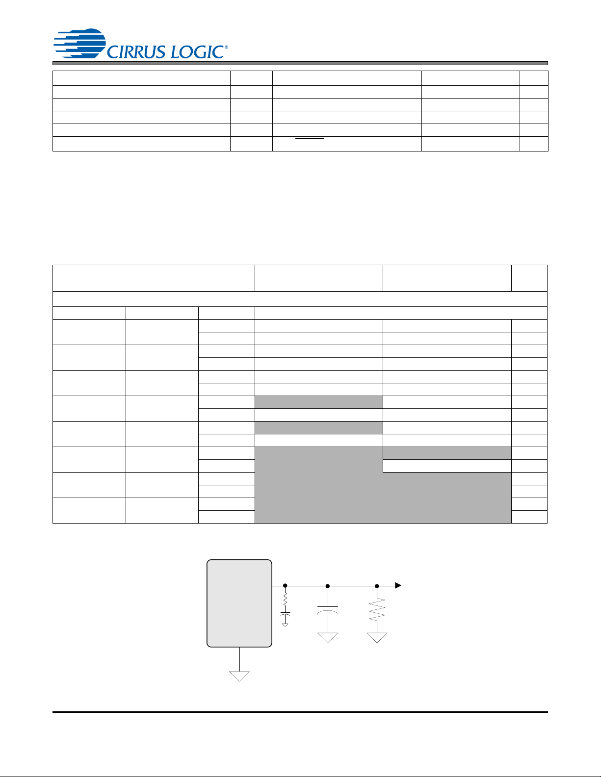
Figure 2. Headphone Output Test Load
CS42L52
Parameters (Note 10) Symbol Conditions Min Typ Max Units
MOSFET On Resistance R
MOSFET On Resistance R
DS(ON)
DS(ON)
Efficiency VP = 5.0 V, P
Output Operating Peak Current I
VP Input Current During Reset I
PC
VP
VP = 3.7V, Id = 0.5 A - 640 - m
VP = 2.5V, Id = 0.5 A - 760 - m
= 2 x 0.8 W, RL = 8 -81-%
O
--1.5A
RESET, pin 32, is held low
-0.85.0µA
9. The PWM driver should be used in captive speaker systems only.
10. Optimal PWM performance is achieved when MCLK > 12 MHz.
HEADPHONE OUTPUT POWER CHARACTERISTICS
Test conditions (unless otherwise specified): Input test signal is a full-scale 997 Hz sine wave; Sample Frequency = 48 kHz;
Measurement Bandwidth is 20 Hz to 20 kHz; Test load RL = 16 CL = 10 pF (see Figure 2); “Required Initialization Settings”
on page 37 written on power up.
Parameters VA = 2.5V
AOUTx Power Into R
= 16
L
Min Typ Max
Min Typ Max
VA = 1.8V
Unit
HP_GAIN[2:0] Analog Gain (G) VHP
000 0.3959 1.8 V - 14 - - 7 - mW
2.5 V - 14 - - 7 - mW
001 0.4571 1.8 V - 19 - - 10 - mW
2.5 V - 19 - - 10 - mW
010 0.5111 1.8 V - 23 - - 12 - mW
2.5 V - 23 - - 12 - mW
011 (default) 0.6047 1.8 V (Note 11) -17 -mW
2.5 V - 32 - - 17 - mW
100 0.7099 1.8 V (Note 11) -23 -mW
2.5 V - 44 - - 23 - mW
101 0.8399 1.8 V (Note 7), Figure 22 on page 74 mW
2.5 V -32 -mW
110 1.0000 1.8 V (Note 7, 11) See Figures 22 an d 23 on page 74 mW
2.5 V mW
111 1.1430 1.8 V mW
2.5 V mW
rms
rms
rms
rms
rms
rms
rms
rms
rms
rms
rms
rms
rms
rms
rms
rms
11. VHP settings lower than VA reduces the headroom of the headphone amplifier. As a result, the DAC
may not achieve the full THD+N performance at full-scale output voltage and power.
18 DS680F2
Page 19
3/1/13
CS42L52
LINE OUTPUT VOLTAGE LEVEL CHARACTERISTICS
Test conditions (unless otherwise specified): Input test signal is a full-scale 997 Hz sine wave; measurement bandwidth is 20 Hz
to 20 kHz; Sample Frequency = 48 kHz; Test load R
page 37 written on power up.
Parameters VA = 2.5V
AOUTx Voltage Into RL = 10 k
HP_GAIN[2:0] Analog
Gain (G)
000 0.3959 1.8 V - 1.34 - - 0.97 - V
001 0.4571 1.8 V - 1.55 - - 1.12 - V
010 0.5111 1.8 V - 1.73 - - 1.25 - V
011 (default) 0.6047 1.8 V - 2.05 - 1.41 1.48 1.55 V
100 0.7099 1.8 V - 2.41 - - 1.73 - V
101 0.8399 1.8 V - 2.85 - 2.05 V
1 1 0 1.0000 1.8 V - 3.39 - - 2.44 - V
111 1.1430 1.8 V (See (Note 11) -2.79-V
VHP
2.5 V - 1.34 - - 0.97 - V
2.5 V - 1.55 - - 1.12 - V
2.5 V - 1.73 - - 1.25 - V
2.5 V 1.95 2.05 2.15 - 1.48 - V
2.5 V - 2.41 - - 1.73 - V
2.5 V - 2.85 - - 2.05 - V
2.5 V - 3.39 - - 2.44 - V
2.5 V - 3.88 - - 2.79 - V
= 10 k CL = 10 pF (see Figure 2); “Required Initialization Settings” on
L
Min Typ Max
VA = 1.8V
Min Typ Max
Unit
pp
pp
pp
pp
pp
pp
pp
pp
pp
pp
pp
pp
pp
pp
pp
pp
COMBINED DAC INTERPOLATION AND ONCHIP ANALOG FILTER RESPONSE
Parameters (Note 12) Min Typ Max Unit
Frequency Response 10 Hz to 20 kHz -0.01 - +0.08 dB
Passband to -0.05 dB corner
to -3 dB corner
StopBand 0.5465 - - Fs
StopBand Attenuation (Note 13) 50 - - dB
Group Delay - 9/Fs - s
De-emphasis Error Fs = 32 kHz
Fs = 44.1 kHz
Fs = 48 kHz
12. Response is clock dependent and scales with Fs. Note that the response plots (Figures 30 and 33 on
page 78) have been normalized to Fs and can be de-normalized by multiplying the X-axis scale by Fs.
13. Measurement Bandwidth is from Stopband to 3 Fs.
0
0
-
-
-
-
-
-
-
-
0.4780
0.4996
+1.5/+0
+0.05/-0.25
-0.2/-0.4
Fs
Fs
dB
dB
dB
DS680F2 19
Page 20
3/1/13
t
h(SK-SDO)
//
//
//
//
//
//
//
//
t
s(SD-SK)
MSB
MSB
MSB-1
MSB-1
LRCK
SCLK
SDOUT
SDIN
t
d(MSB)
t
s(LK-SK)
t
P
t
h
t
s(SDO-SK)
Figure 3. Serial Audio Interface Timing
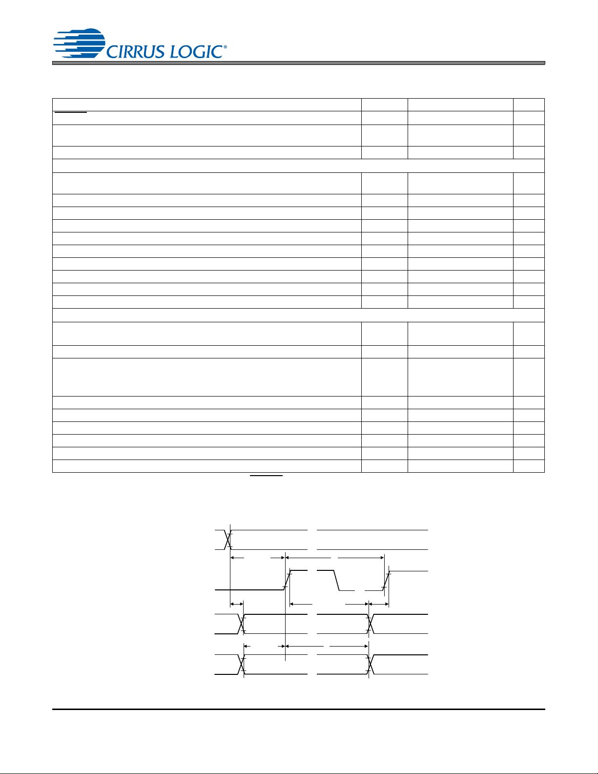
SWITCHING SPECIFICATIONS - SERIAL PORT
Inputs: Logic 0 = DGND, Logic 1 = VL, SDOUT C
Parameters Symbol Min Max Units
RESET
MCLK Frequency (Note 15)
MCLK Duty Cycle
pin Low Pulse Width (Note 14)
Slave Mode
Input Sample Rate (LRCK)
LRCK Duty Cycle
SCLK Frequency
SCLK Duty Cycle
LRCK Setup Time Before SCLK Rising Edge
LRCK Edge to SDOUT MSB Output Delay
SDOUT Setup Time Before SCLK Rising Edge
SDOUT Hold Time After SCLK Rising Edge
SDIN Setup Time Before SCLK Rising Edge
SDIN Hold Time After SCLK Rising Edge
Master Mode
Output Sample Rate (LRCK) All Speed Modes
LRCK Duty Cycle
SCLK Frequency SCLK=MCLK mode
SCLK Duty Cycle
LRCK Edge to SDOUT MSB Output Delay
SDOUT Setup Time Before SCLK Rising Edge
SDOUT Hold Time After SCLK Rising Edge
SDIN Setup Time Before SCLK Rising Edge
SDIN Hold Time After SCLK Rising Edge
14. After powering up the CS42L52, RESET should be held low after the power supplies and clocks are
settled.
15. See “Example System Clock Frequencies” on page 76 for typical MCLK frequencies.
LOAD
= 15 pF.
MCLK=12.0000 MHz
all other modes
F
s
1/t
P
t
s(LK-SK)
t
d(MSB)
t
s(SDO-SK)
t
h(SK-SDO)
t
s(SD-SK)
t
h
F
s
1/t
P
1/t
P
1/t
P
t
d(MSB)
t
s(SDO-SK)
t
h(SK-SDO)
t
s(SD-SK)
t
h
CS42L52
1-ms
(See “Serial Port Clock-
ing” on page 33)
45 55 %
(See “Serial Port Clock-
ing” on page 33)
45 55 %
-64•FsHz
45 55 %
40 - ns
-52ns
20 - ns
30 - ns
20 - ns
20 - ns
(See “Serial Port Clock-
ing” on page 33)
45 55 %
- 12.0000 MHz
-68•FsHz
-64•FsHz
45 55 %
-52ns
20 - ns
30 - ns
20 - ns
20 - ns
MHz
kHz
Hz
20 DS680F2
Page 21
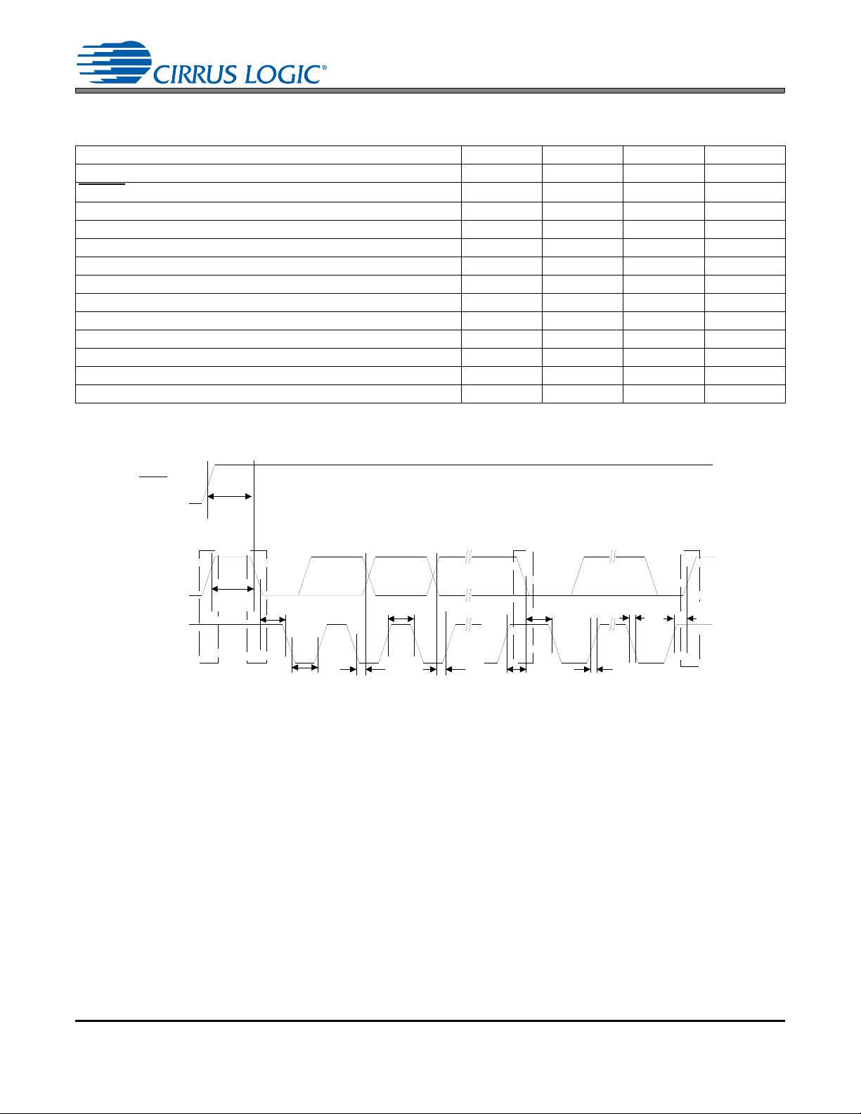
3/1/13
t
buf
t
hdst
t
hdst
t
low
t
r
t
f
t
hdd
t
high
t
sud
t
sust
t
susp
Stop Start
Start
Stop
Repeated
SDA
SCL
t
irs
RST
Figure 4. Control Port Timing - I²C
SWITCHING SPECIFICATIONS - I²C CONTROL PORT
Inputs: Logic 0 = DGND, Logic 1 = VL, SDA CL=30pF.
Parameters Symbol Min Max Unit
SCL Clock Frequency
RESET Rising Edge to Start
Bus Free Time Between Transmissions
Start Condition Hold Time (prior to first clock pulse)
Clock Low time
Clock High Time
Setup Time for Repeated Start Condition
SDA Hold Time from SCL Falling (Note 16)
SDA Setup time to SCL Rising
Rise Time of SCL and SDA
Fall Time SCL and SDA
Setup Time for Stop Condition
Acknowledge Delay from SCL Falling
16. Data must be held for sufficient time to bridge the transition time, tfc, of SCL.
f
t
t
t
hdst
t
low
t
high
t
sust
t
hdd
t
sud
t
t
t
susp
t
ack
scl
irs
buf
rc
fc
CS42L52
- 100 kHz
550 - ns
4.7 - µs
4.0 - µs
4.7 - µs
4.0 - µs
4.7 - µs
0-µs
250 - ns
-1µs
- 300 ns
4.7 - µs
300 1000 ns
DS680F2 21
Page 22
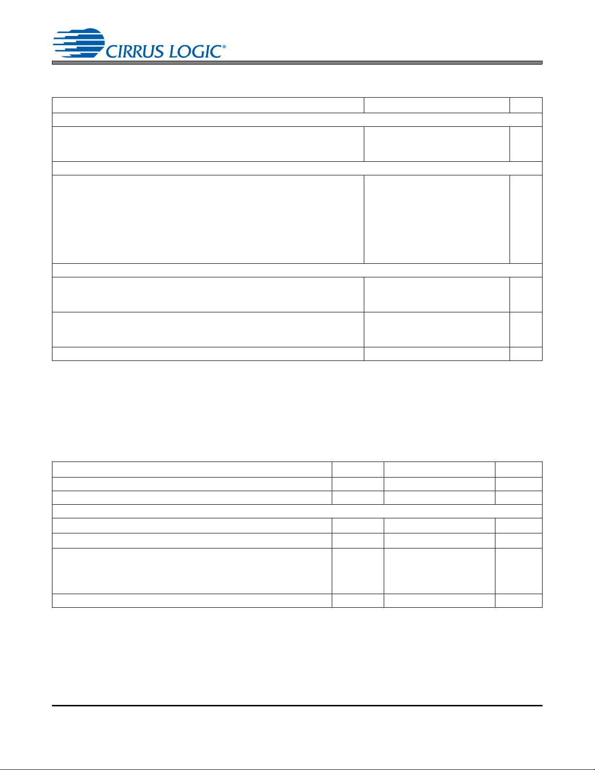
3/1/13
CS42L52
DC ELECTRICAL CHARACTERISTICS
AGND = 0 V; All voltages with respect to ground.
Parameters Min Typ Max Units
VQ Characteristics
Nominal Voltage
Output Impedance
DC Current Source/Sink
MIC BIAS Characteristics
Nominal Voltage BIASLVL[2:0] = 000
BIASLVL[2:0] = 001
BIASLVL[2:0] = 010
BIASLVL[2:0] = 011
BIASLVL[2:0] = 100
BIASLVL[2:0] = 101
DC Output Current
Power Supply Rejection Ratio (PSRR) 1 kHz
Power Supply Rejection Ratio Characteristics
PSRR @1 kHz (Note 17) PGA to ADC
ADC
DAC (HP and Line Amps)
PSRR @60 Hz (Note 17) PGA to ADC
DAC (HP and Line Amps)
PSRR @217 Hz Full-Bridge PWM Outputs - 56 - dB
(Note 18)
ADC
-
-
-
-
-
-
-
-
-
-
-
-
-
-
-
-
-
0.5•VA
23
-
0.5•VA
0.6•VA
0.7•VA
0.8•VA
0.83•VA
0.91•VA
-
50
44
60
60
22
42
60
-
-
1
-
-
-
-
-
-
1
-
-
-
-
-
-
-
V
k
A
V
V
V
V
V
V
mA
dB
dB
dB
dB
dB
dB
dB
17. Valid with the recommended capacitor values on FILT+ and VQ. Increasing the capacitance will also
increase the PSRR.
18. The PGA is biased with VQ, created from a resistor divider from the VA supply. Increasing the capacitance on VQ will also increase the PSRR at low frequencies. A 10 µF capacitor on VQ improves the
PSRR to 42 dB.
DIGITAL INTERFACE SPECIFICATIONS AND CHARACTERISTICS
Parameters (Note 19) Symbol Min Max Units
Input Leakage Current I
Input Capacitance -10pF
1.8 V - 3.3 V Logic
High-Level Output Voltage (I
Low-Level Output Voltage (I
High-Level Input Voltage VL = 1.65 V
Low-Level Input Voltage V
= -100 A) V
OH
= 100 A) V
OL
VL = 1.8 V
VL = 2.0 V
VL > 2.0 V
in
OH
OL
V
IH
IL
19. See “I/O Pin Characteristics” on page 10 for serial and control port power rails.
-±10A
VL - 0.2 - V
-0.2V
0.85•VL
0.77•VL
0.68•VL
0.65•VL
- 0.30•VL V
-
-
-
-
V
V
V
V
22 DS680F2
Page 23
3/1/13
POWER CONSUMPTION See (Note 20).
Power Ctl. Registers Typical Current (mA)
Operation
1
Off (Note 21)
Standby (Note 22) xxxx1xxxx x x x
2
Mono Record ADC 1 110011111111111
3
PGA to ADC1010011111111111
MIC to PGA to ADC
MIC to PGA to ADC
Stereo Record ADC1100011111111111
4
MIC to PGA to ADC
Mono Playback to Headphone 1 111011110111111
5
Mono Playback to Speaker 1 111011111111010
6
Stereo Playback to Headphone 1 111011110101111
7
Stereo Playback to Speaker 1111011111111010
8
Stereo Passthrough to Head-
9
phone
Mono Record and Playback
10
PGA in (no MIC) to Mono HP
Phone Monitor
11
MIC (w/bias) in to Mono Out
Stereo Record and Playback
12
PGA in (no MIC) to St. HP Out
Stereo Rec. and Full Playback
13
PGA (no MIC) to St. HP and SPK
(with Bias)
(no Bias)
PGA to ADC0000011111111111
(no Bias)
02h 03h 04h
PDN_PGAB
PDN_PGAA
PDN_ADCB
PDN_ADCA
PDN
PDN_MICB
PDN_MICA
PDN_MICBIAS
PDN_HPB[1:0]
xxxxxxxxx x x x
1010010011111111
1010010111111111
0000000111111111
1111011110101111
1010011111101111
1010010011101111
0000011110101111
0000011110101010
PDN_HPA[1:0]
i
VHPiVA
PDN_SPKB[1:0]
PDN_SPKA[1:0]
V
1.8 0.00 0.00 0.00
2.5 0.00 0.00 0.00 0.00
1.8 0.00 0.00 0.01
2.5 0.00 0.00 0.02 0.05
1.8 0.00 1.67 2.32
2.5 0.00 1.87 3.72 14.05
1.8 0.00 2.1 2.31
2.5 0.00 2.3 3.72 15.13
1.8 0.00 3.48 2.32
2.5 0.00 3.71 3.72 18.65
1.8 0.00 3.15 2.32
2.5 0.00 3.37 3.73 17.83
1.8 0.00 2.31 2.37
2.5 0.00 2.53 3.82 15.95
1.8 0.00 3.18 2.37
2.5 0.00 3.42 3.81 18.15
1.8 0.00 5.32 2.37
2.5 0.00 5.57 3.81 23.53
1.8 1.59 1.99 2.72
2.5 2.07 2.62 4.27 22.43
1.8 0.00 0.20 4.42
2.5 0.00 0.22 6.77 21.21
1.8 2.77 2.00 2.91
2.5 3.27 2.63 4.28 25.48
1.8 0.00 0.20 4.38
2.5 0.00 0.22 6.80 21.28
1.8 2.79 1.91 1.06
2.5 3.18 2.14 1.81 17.85
1.8 1.77 3.95 4.28
2.5 2.13 4.77 6.63 33.90
1.8 1.76 5.33 4.28
2.5 2.15 6.19 6.69 37.65
1.8 2.76 5.05 4.64
2.5 3.21 5.90 7.17 40.78
1.8 3.49 5.24 7.20
2.5 3.95 6.10 10.46 55.07
i
VD
i
VL
VL=3.3V
(Note 23)
0.00 0.00
0.00 0.00
0.03 0.00
0.03 0.00
0.03 0.00
0.03 0.00
0.03 0.00
0.03 0.00
0.03 0.00
0.01 0.00
0.01 1.00
0.01 0.00
0.01 1.00
0.01 0.00
0.03 0.00
0.03 0.00
0.03 0.00
0.03 1.00
CS42L52
i
VP
VP=3.7V
Total
Power
(mW
0.00
0.02
7.24
7.99
10.49
9.90
8.48
10.04
13.90
11.36
12.05
13.84
11.98
10.39
18.05
20.52
22.46
32.47
rms
)
20. Unless otherwise noted, test conditions are as follows: All zeros input, slave mode, sample
rate = 48 kHz; No load. Digital (VD) and logic (VL) supply current will vary depending on speed mode
and master/slave operation. “Required Initialization Settings” on page 37 written on power up.
21. RESET
22. RESET
pin 25 held LO, all clocks and data lines are held LO.
pin 25 held HI, all clocks and data lines are held HI.
23. VL current will slightly increase in master mode.
DS680F2 23
Page 24

4. APPLICATIONS
4.1 Overview
4.1.1 Basic Architecture
The CS42L52 is a highly integrated, low-power, 24-bit audio CODEC comprised of a stereo analog-todigital converter (ADC), a stereo digital-to-analog converter (DAC), a digital PWM modulator and two fullbridge power back-ends. The ADC and DAC are designed using multibit delta-sigma techniques - the
DAC operates at an oversampling ratio of 128Fs and the ADC oper ates at 64Fs, where Fs is equal to the
system sample rate.
The different clock rates maximize power savings while maintaining high performance. The PWM modulator operates at a fixed frequency of 384 kHz. The power FETs are configure d for either stereo full-bridge
or mono parallel full-bridge output. The CODEC operates in one of four sample rate speed modes: Quar ter, Half, Single, and Double. It accepts and is capable of generating serial port clocks (SCLK, LRCK) derived from an input Master Clock (MCLK).
4.1.2 Line and MIC Inputs
The analog input portion of the CODEC allows selection from and configuration of multiple combinations
of stereo and microphone (MIC) sources. Eight line inputs with an option for two balanced MIC inputs, a
MIC bias output, and a Programmable Gain Amplifier (PGA) comprise the analog front- end.
3/1/13
CS42L52
4.1.3 Line and Headphone Outputs
The analog output portion of the CODEC includes a headphone amplifier capable of driving headphone
and line-level loads. An on-chip charge pump creates a negative headphone supply allowing a full-scale
output swing centered around groun d. Th is elim in at es the need for large DC-Blocking capacitors and allows the amplifier to deliver more power to headphone loads at lower supply voltages.
4.1.4 Speaker Driver Outputs
The Class D power amplifiers drive 8 ohm (stereo) and 4 ohm (mono ) speakers d irectly, without the ne ed
for an external filter. The power MOSFETS are powered directly from a battery eliminating the efficiency
loss associated with an external regulator. Battery level monitoring and compensation maintains a stead y
output as battery levels fall. NOTE: The CS42L52 should only be used in captive speaker systems where
the outputs are permanently tied to the speaker terminals.
4.1.5 Fixed Function DSP Engine
The fixed-function digital signal processing engine processes both the PCM serial input data and ADC
output data, allowing a mix between the two. Independent volume control, le ft/right channel swaps, mono
mixes, tone control, and limiting functions also comprise the DSP engine.
4.1.6 Beep Generator
The beep generator delivers tones at select frequencies across approximately two octave major scales.
With independent volume control, beeps may be configured to occur continuously, perio dically, or at single time intervals.
4.1.7 Power Management
Three control registers provide independent power-down control of the ADC, DAC, PGA, MIC pre-amp,
MIC bias, Headphone, and Speaker outputs, allowing operation in select applications with minimal power
consumption.
24 DS680F2
Page 25
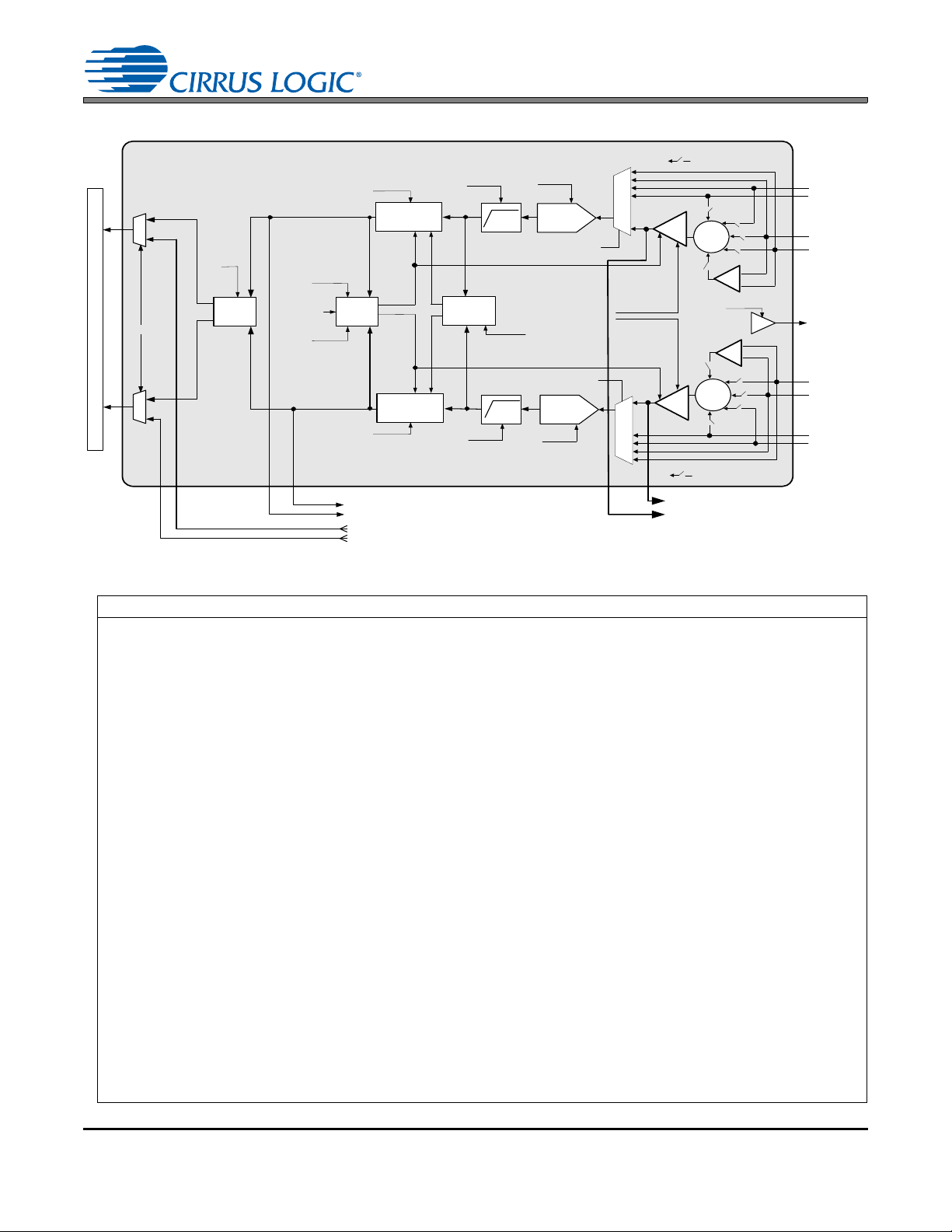
4.2 Analog Inputs
`
AIN4A/ MIC1+/
MIC2A
Gain A d jus t
ALC
PDN_PGAA
PGAA VOL[5:0]
ADCB=A
ANLGSFTA
ANLGZCA
HPFRZA
HPFA
HPFA_CF[1:0]
PDN_ADCA
INV_ADCA
PDN_CHRG
ALCB
ALCBSRDIS
ALCBZCDIS
MICBIAS
BIASLVL[2:0]
PDN_BIAS
PCM Serial Interface
TO DSP Engine
ALCARATE[5:0]
ALCRRATE[5:0]
MAX[2:0]
MIN[2:0]
ALCA
ALCASRDIS
ALCAZCDIS
AIN1A
AIN2A
= PGAASEL[5:1]
ADC
PDN_PGAB
PGAB VOL[5:0]
ADCB=A
ANLGSFTB
ANLGZCB
ADCBMUTE
DIGSFT
DIGZC
ADCBVOL[7:0]
+24/-96dB
1dB steps
HPFRZB
HPB
HPFB_CF[1:0]
PDN_ADCB
INV_ADCB
PDN_CHRG
Noise Gate
NGALL
NG
THRESH[3:0 ]
NGDELAY[1:0]
Gain Adjust
FROM DSP ENGINE
DIGMIX
AIN3A/MIC1-/
MIC1A
AIN4B/ MIC2+/
MIC2B
AIN1B
AIN2B
AIN3B/MIC2-/
MIC1B
ANALOG PASS THRU TO
HEADPHONE AMPLIFIER MU X
Swap/
Mix
DIGSUM[1:0]
ADCAMUTE
DIGSFT
DIGZC
ADCAVOL[7:0]
+24/-96dB
1dB steps
Refer to
“MIC Inp uts ”
ADC
ADCASEL[2:0]
ADCBSEL[2:0]
= PGABSEL[5:1]
Refer to
“MIC Inp uts ”
Figure 5. Analog Input Signal Flow
3/1/13
CS42L52
Referenced Control Register Location
Analog Front End
PDN_PGAx .........................
PGAxVOL[5:0].....................
ADCB=A..............................
ANLGSFTx..........................
ANLGZCx............................
ADCxSEL[2:0].....................
PGAxSEL5,4,3,2,1..............
BIASLVL[2:0].......................
PDN_BIAS...........................
PDN_ADCx .........................
PDN_CHRG........................
INV_ADCx...........................
HPFRZx...............................
HPFx ...................................
HPFx_CF[1:0]......................
ADCxOVFL..........................
Digital Volume
ADCxMUTE.........................
ADCxVOL............................
ALCx....................................
ALCxSRDIS.........................
ALCxZCDIS.........................
ALCARATE[5:0]...................
ALCRRATE[5:0]..................
MAX[2:0]..............................
MIN[2:0]...............................
NGALL.................................
NG.......................................
THRESH[3:0].......................
NGDELAY[1:0]....................
Miscellaneous
DIGSUM[1:0].......................
DIGMUX..............................
DS680F2 25
“Power Down PGAx” on page 42
“PGAx Volume” on page 56
“Analog Front-End Volume Setting B=A” on page 50
“Ch. x Analog Soft Ramp” on page 49
“Ch. x Analog Zero Cross” on page 49
“ADC Input Select” on page 48
“PGA Input Mapping” on page 49
“MIC Bias Level” on page 48
“Power Down MIC Bias” on page 43
“Power Down ADCx” on page 43
“Power Down ADC Charge Pump” on page 42
“Invert ADC Signal Polarity” on page 51
“ADCx High-Pass Filter Freeze” on page 49
“ADCx High-Pass Filter” on page 49
“HPF x Corner Frequency” on page 50
“ADCx Overflow (Read Only)” on page 71
“ADC Mute” on page 51
“ADCx Volume” on page 57
“ALCx Enable” on page 67
“ALCx Soft Ramp Disable” on page 55
“ALCx Zero Cross Disable” on page 56
“ALC Attack Rate” on page 67
“ALC Release Rate” on page 68
“ALC Maximum Threshold” on page 68
“ALC Minimum Threshold” on page 69
“Noise Gate All Channels” on page 69
“Noise Gate Enable” on page 69
“Noise Gate Threshold and Boost” on page 70
“Noise Gate Delay Timing” on page 70
“Digital Sum” on page 50
“Digital MUX” on page 50
Page 26
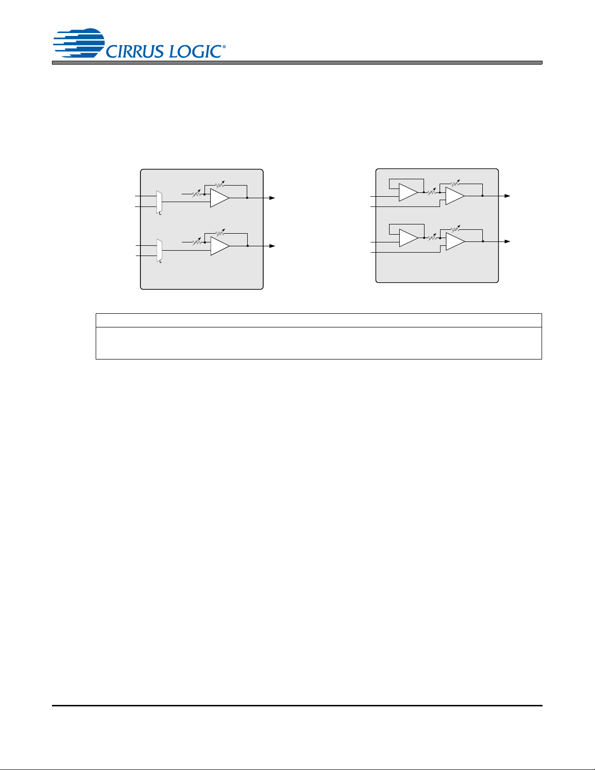
4.2.1 MIC Inputs
MIC1-
-
+
+
MIC1+
MIC2-
-
+
-
+
MIC2+
23
21
24
22
MICACFG=’1'b
MICBCFG=’1'b
MICAGAIN[4:0]
MICBGAIN[4:0]
16..32 dB/
1 dB steps
16..32 dB/
1 dB steps
PDN_MICA=’0'b
PDN_MICB=’0'b
to summing
PGA A
Note: Output to PGA = (MIC+ - MIC-)*gain + MIC
-
to summing
PGA B
MIC1A
-
+
MIC2A
MIC1B
-
+
MIC2B
23
21
24
22
MICACFG=’0'b
MICBCFG=’0'b
MICAGAIN[4:0]
MICBGAIN[4:0]
16..32 dB/
1 dB steps
16..32 dB/
1 dB steps
PDN_MICA=’0'b
PDN_MICB=’0'b
MICASEL
MICBSEL
to summing
PGA A
to summing
PGA B
VQ
VQ
Figure 6. Single-Ended MIC Configuration Figure 7. Differential MIC Configuration
The input pins 21, 22, 23, and 24 accept stereo line-level or microphone signals. For microphone inputs,
either single-ended or differential configuration is allowed, providing programmable pre-amplification of
low-level signals. In the single-ended configuration, an internal MUX chooses one of two stereo sets (s election is made independently on channels A and B). In the differential configuration, an internal voltage
follower cascaded with the pre-amplifier maintains high input impedance and provides noise rejection
above the MICxGAIN setting. The pre-amps are biased to VQ in both configurations.
3/1/13
CS42L52
Referenced Control Register Location
MICxCFG............................
PDN_MICx..........................
MICxGAIN...........................
“MICx Configuration” on page 55
“Power Down MICx” on page 43
“MICx Gain” on page 55
4.2.2 Automatic Level Control (ALC)
When enabled, the ALC monitors the analog input signal after the digital attenuator, detects when peak
levels exceed the maximum (MAX) threshold settings, and responds by applying attenuation as necessary to maintain the resulting level below the MAX threshold. To apply this attenuation, the ALC first lowers the PGA gain settings and then increases the digital attenuation levels. All attenuation is applied at a
programmable attack rate.
When input signal levels fall below the minimum (MIN) threshold, the ALC responds by removing any attenuation that it has previously applied until all ALC-applied attenuation has been removed or until the
MAX threshold is again crossed. To remov e th is at te nu at ion , th e AL C firs t de cr ea se s the dig ita l att en uation levels and then increases the PGA gain. All attenuation is removed at a programmable release rate.
It should be noted that the ALC is applied independently to channels A and B with one exception: the input
signals on both channels A and B must be below the MIN threshold in order for the ALC attenuation to be
released on channel B.
Attack and release rates are affected by the ADC soft-r amp/zero-cross settings and sample ra te, Fs. ALC
soft-ramp and zero-cross dependency may be independently enabled/disabled.
Recommended settings: Best level control may be realized with the fastest attack and slowest release
setting with soft ramp enabled in the control registers.
Notes:
1. When ALC x is enabled and the PGAxVOL[5:0] is set above 12 dB, the ADCxVOL[7:0] should not be
set below 0 dB.
2. The maximum realized gain must be set in the PGAxVOL register. The ALC will only apply the gain
set in the PGAxVOL.
3. The ALC maintains the output signal between the MIN/MAX thresholds. As input signal level changes,
the level-controlled output may not always be the same but always falls within the thresholds.
26 DS680F2
Page 27
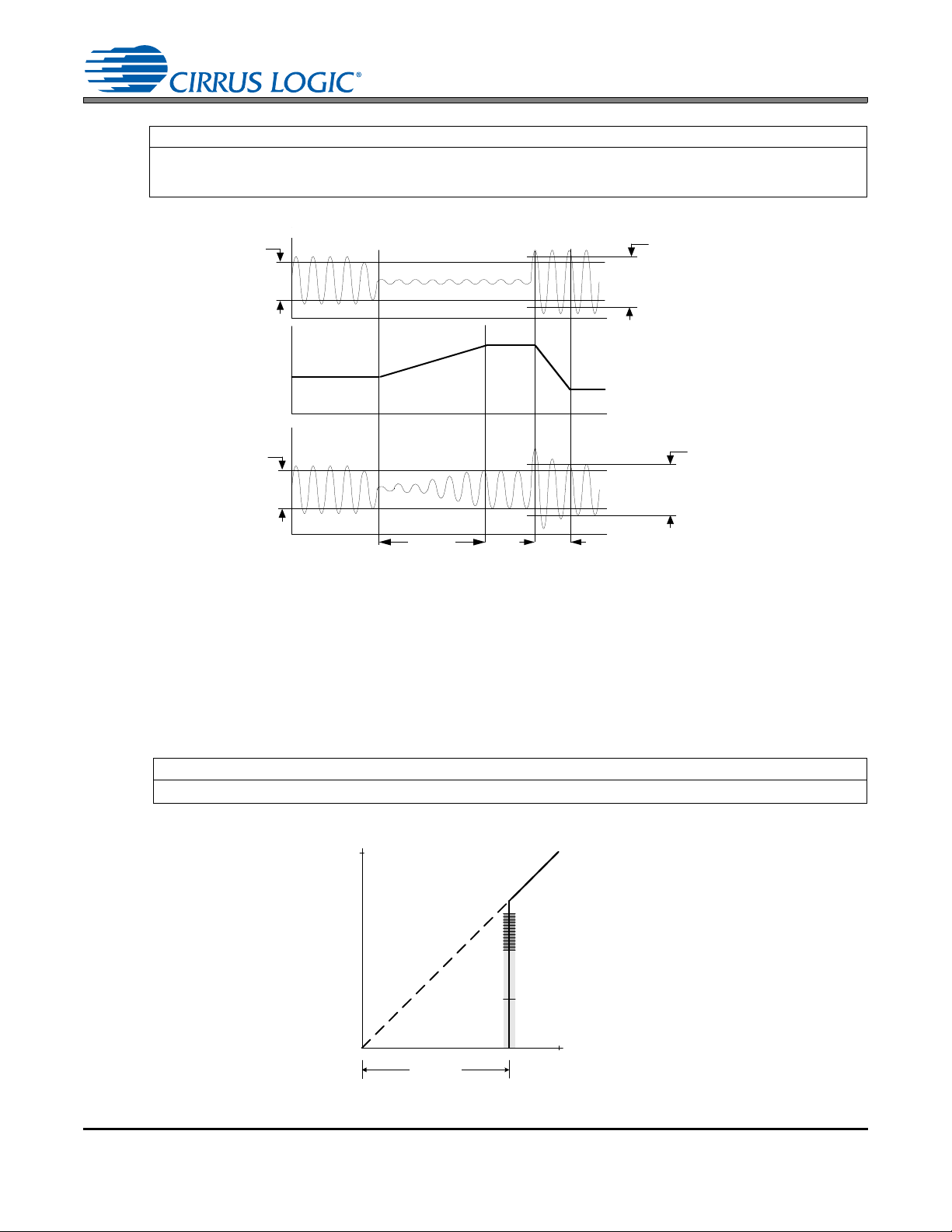
Output
(after A L C )
Input (before ALC)
RRATE[5:0]
PGA G ain and/or
Attenuator
ALC
Response
MAX[2:0]
ARATE[5:0
]
below f u ll s c ale
MIN[2:0]
below fu ll s cale
MIN[2:0]
below f u ll s c a le
MAX[2:0]
below f u ll s c a le
Figure 8. ALC
-96 -40
THRESH[2:0]
Maximum Attenuation*
-52 dB
Output
(dB)
Input (dB)
N
G
E
N
=
1
N
G
E
N
=
0
-80 dB
-64 dB
Figure 9. Noise Gate Attenuation
Referenced Control Register Location
PGAxVOL[5:0
MAX[2:0], MIN[2:0]
“PGAx Vol. and ALCx Transition Ctl.: ALC, PGA A (Address 12h) and ALC, PGA B (Address 13h)” on
“ALC Threshold (Address 2Ch)” on page 68
3/1/13
CS42L52
page 55
4.2.3 Noise Gate
The noise gate may be used to mute signal levels that fall below a programmable thre shold. This prevents
the ALC from applying gain to noise. A programma ble delay may be used to set the minimum time before
the noise gate attacks the signal.
Note: Maximum noise gate attenuation levels will depend on the gain applied in either the PGA or MIC
pre-amplifier. For example: If both +32 dB pre- amplification and +12 dB programmable gain is applied,
the maximum attenuation that the noise gate achieves will be 52 dB (-96 + 32 + 12) below full-scale.
Referenced Control Register Location
Noise Gate Controls............ “Noise Gate Control (Address 2Dh)” on page 69
DS680F2 27
Page 28
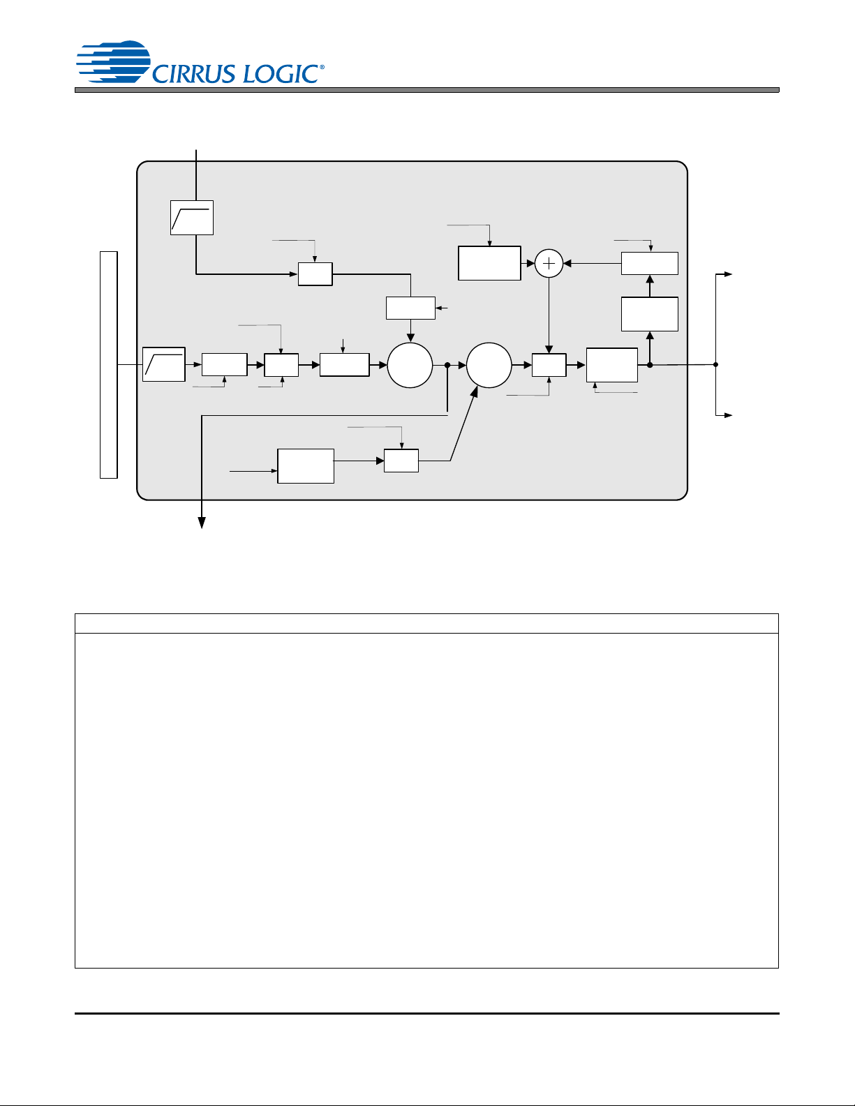
4.3 Analog Outputs
Beep
Generator
VOL
Bass/
Treble/
Control
VOL
Peak
Detect
Limiter
Chnl Vol.
Settings
Channel
Swap
Demph
VOL
VOL
+12dB/-102dB
0.5dB steps
MSTAVOL[7:0]
MSTBVOL[7:0]
+12dB/-51.5dB
0.5dB steps
AMIXAMUTE
AMIXBMUTE
AMIXAVOL[6:0]
AMIXBVOL[6:0]
+12dB/-51.5dB
0.5dB steps
PMIXAMUTE
PMIXBMUTE
PMIXAVOL[6:0]
PMIXBVOL[6:0]
0dB/-50dB
2.0dB steps
BPVOL[4:0]
DEEMPH
TC_EN
BASS_CF[1:0]
TREB_CF[1:0]
BASS[3:0]
TREB[3:0]
+12.0dB/-10.5dB
1.5dB steps
Fixed Function DSP
MSTAMUTE
MSTBMUTE
DIGSFT
DIGZC
PLYBCKB=A
LIMARATE[7:0]
LIMRRATE[7:0]
LMAX[2:0]
CUSH[2:0]
LIMSRDIS
LIMZCDIS
LIMIT
PCMASWAP[1:0]
PCMBSWAP[1:0]
PCM Serial Interface
INPUTS FROM ADCA
and ADCB
OFFTIME[2:0]
ONTIME[3:0]
FREQ[3:0]
BEEP[1:0]
BEEPMIXDIS
Digital Mix to ADC
Serial Interface
Channel
Swap
INV_PCMA
INV_PCMB
ADCASWAP[1:0]
ADCBSWAP[1:0]
PWM
Modulator
DAC
Figure 10. DSP Engine Signal Flow
3/1/13
CS42L52
Referenced Control Register Location
DSP
DEEMPH.............................
PMIXxMUTE........................
PMIXxVOL[6:0]....................
INV_PCMx...........................
PCMxSWAP[1:0].................
AMIXxMUTE........................
AMIXxVOL[6:0]....................
ADCxSWAP[1:0]..................
MSTxVOL[7:0].....................
MSTxMUTE.........................
DIGSFT...............................
DIGZC.................................
PLYBCKB=A........................
TC_EN.................................
BASS_CF[1:0].....................
TREB_CF[1:0].....................
BASS[3:0]................ ............
TREB[3:0]............................
LIMIT...................................
LIMSRDIS ...........................
LIMZCDIS............................
LMAX[2:0]............................
CUSH[2:0]...........................
LIMARATE[7:0]....................
LIMRRATE[7:0]...................
“HP/Speaker De-emphasis” on page 53
“PCM Mixer Channel x Mute” on page 58
“PCM Mixer Channel x Volume” on page 58
“Invert PCM Signal Polarity” on page 52
“PCM Mix Channel Swap” on page 64
“ADC Mixer Channel x Mute” on page 58
“ADC Mixer Channel x Volume” on page 58
“ADC Mix Channel Swap” on page 64
“Master Volume Control” on page 63
“Master Playback Mute” on page 52
“Digital Soft Ramp” on page 53
“Digital Zero Cross” on page 53
“Playback Volume Setting B=A” on page 51
“Tone Control Enable” on page 62
“Bass Corner Frequency” on page 62
“Treble Corner Frequency” on page 62
“Bass Gain” on page 63
“Treble Gain” on page 62
“Peak Detect and Limiter” on page 66
“Limiter Soft Ramp Disable” on page 65
“Limiter Zero Cross Disable” on page 66
“Limiter Maximum Threshold” on page 65
“Limiter Cushion Threshold” on page 65
“Limiter Attack Rate” on page 67
“Limiter Release Rate” on page 66
28 DS680F2
Page 29
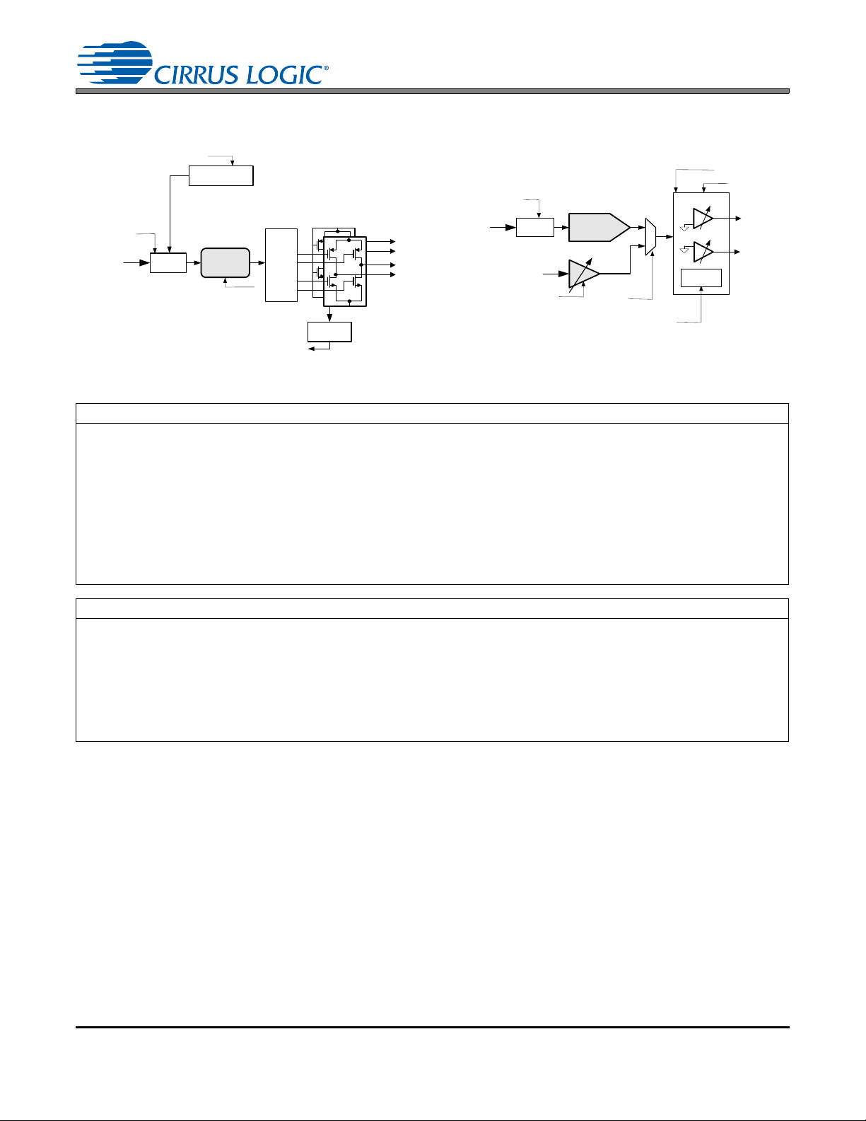
Referenced Control Register Location
Charge
Pump
DAC
CHGF REQ[3 :0 ]
HPGA IN [2:0]
VOL
VOL
Analog Passthru
from PGA
HPAMUTE
HPBMUTE
HPA_VOL[7:0]
HPB_VOL[7:0]
+0dB/-102dB
0.5dB steps
PASSAMUTE
PASSBMUTE
PASSAVOL[7:0]
PASSBVOL[70]
+12dB/-60dB
0.5dB steps
(uses PGA)
PASSTHRUA
PASSTHRUB
PDN_HPA[1:0]
PDN_HPB[1:0]
A
B
from D S P
Engine
HP/Line
Outputs
VOL
PWM
Modulator
A
SPKAMUTE
SPKBMUTE
MUTE50/50
SPKMONO
SPKSWAP
SPKB=A
SPKAVOL[7:0]
SPKBVOL[7:0]
+0dB/-102dB
0.5dB steps
PDN_SPKA[1:0]
PDN_SPKB[1:0]
Short
Circuit
SPKASHRT
Battery
Compensation
BATTCMP
VPREF[3:0]
VPLVL[7:0]
SPKBSHRT
+
+
-
Gate
Drive
from DSP
Engine
Speaker
Outputs
B
Figure 11. PWM Output Stage Figure 12. Analog Output Stage
PWM Control
SPKxMUTE.........................
MUTE50/50.........................
SPKMONO..........................
SPKxVOL[7:0].....................
SPKSWAP...........................
SPKB=A ..............................
BATTCMP...........................
VPREF[3:0] .........................
VPLVL[7:0]..........................
PDN_SPKx[1:0]...................
SPKxSHRT..........................
“Speaker Mute” on page 54
“Speaker Mute 50/50 Control” on page 54
“Speaker MONO Control” on page 54
“Speaker Volume Control” on page 64
“Speaker Channel Swap” on page 54
“Speaker Volume Setting B=A” on page 54
“Battery Compensation” on page 71
“VP Reference” on page 72
“VP Voltage Level (Read Only)” on page 72
“Speaker Power Control” on page 44
“Speaker Current Load Status (Read Only)” on page 72
3/1/13
CS42L52
Referenced Control Register Location
Analog Output
HPxMUTE ...........................
HPxVOL[7:0] .......................
PDN_HPx[1:0].....................
HPGAIN[2:0]........................
PASSTHRUx.......................
PASSxMUTE.......................
PASSxVOL[7:0]...................
CHGFREQ ..........................
“Headphone Mute” on page 54
“Headphone Volume Control” on page 63
“Headphone Power Control” on page 44
“Headphone Analog Gain” on page 51
“Passthrough Analog” on page 52
“Passthrough Mute” on page 52
“Passthrough x Volume” on page 57
“Charge Pump Frequency” on page 73
4.3.1 Beep Generator
The Beep Generator generates audio frequencies across approximately two octave major sca les. It offers
three modes of operation: Continuous, multiple, and single (one-shot) beeps. Sixteen on and eight off
times are available.
Note: The Beep is generated before the limiter and may affect desired limiting performance. If the limiter function is used, it may be required to set the beep volume sufficiently below the threshold to prevent
the peak detect from triggering. Since the master volume control, MSTxVOL[7:0], will affect the beep vol-
DS680F2 29
ume, DAC volume may alternatively be controlled using the PMIXxVOL[6:0] bits.
Page 30
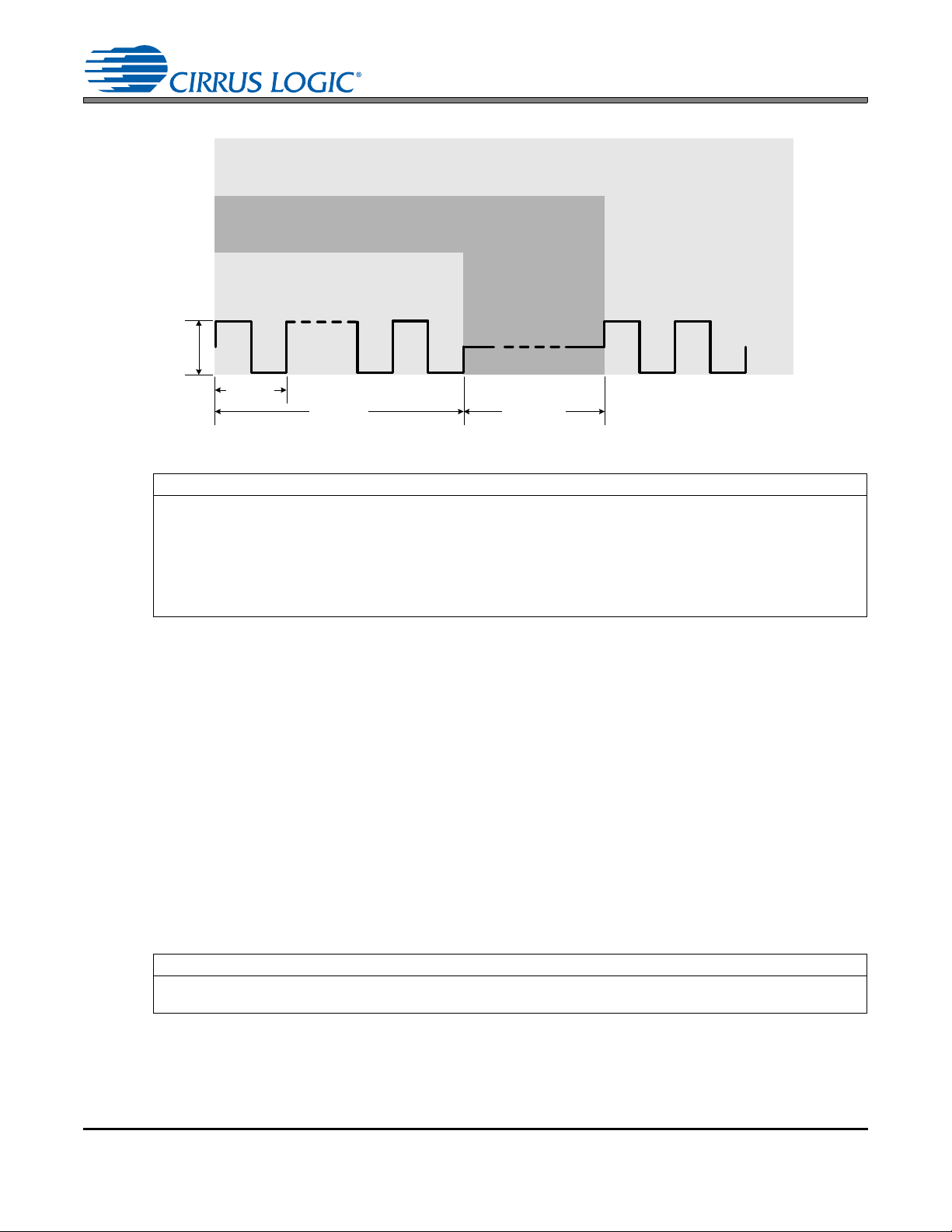
FREQ[3:0]
...
BPVOL[4:0]
ONTIME[3:0] OFFTIME[2:0]
BEEP[1:0] =
'01'
BEEP[1:0] =
'10'
BEEP[1:0] =
'11'
SINGLE-BEEP: Beep turns on at a
configurable frequency (FREQ) and
volume (BPVOL) for the duration of
ONTIME. BEEP must be cleared
and set for additional beeps.
MULTI-BEEP: Beep turns on at a configurable frequency (FREQ)
and volume (BPVOL) for the duration of ONTIME and turns off for
the duration of OFFTIME. On and off cycles are repeated until
BEEP is cleared.
CONTINUOUS BEEP: Beep turns on at a configurable frequency (FREQ) and volume (BPVOL) and remains on
until BEEP is cleared.
Figure 13. Beep Configuration Options
Referenced Control Register Location
MSTxVOL[7:0].....................
PMIXxVOL[6:0] ...................
OFFTIME[2:0] .....................
ONTIME[3:0].......................
FREQ[3:0]...........................
BEEP[1:0]............................
BEEPMIXDIS......................
BPVOL[4:0].........................
“Master Volume Control: MSTA (Address 20h) and MSTB (Address 21h)” on page 63
“PCMx Mixer Volume: PCMA (Address 1Ah) and PCMB (Address 1Bh)” on page 58
“Beep Off Time” on page 60
“Beep On Time” on page 60
“Beep Frequency” on page 59
“Beep Configuration” on page 61
“Beep Mix Disable” on page 61
“Beep Volume” on page 61
3/1/13
CS42L52
4.3.2 Limiter
When enabled, the limiter monitors the digital input signal before th e DAC and PWM mo dulators, detects
when levels exceed the maximum threshold settings, and lowers the master volume at a pr ogram mable
attack rate below the maximum threshold. When the input signa l level falls below the maximum threshold,
the AOUT volume returns to its original level set in the Master Volume Control register at a programmable
release rate. Attack and release rates are affe cted by the DAC soft-r amp/zero -cross settin gs and sample
rate, Fs. Limiter soft-ramp and zero-cross dependency may be independently enabled/di sabled.
Notes:
1. Recommended settings: Best limiting performance may be realized with the fastest attack and
slowest release setting with soft ramp enabled in th e contro l registers. The MIN bits allow the user to
set a threshold slightly below the maximum thresh old for hystere sis control - this cushions the sound
as the limiter attacks and releases.
2. T h e Lim ite r ma in tains th e ou tp ut sign al be twe en the MIN and MAX thresholds. As the digital input
signal level changes, the level-controlled output may not always be the same but will always fall within
the thresholds.
Referenced Control Register Location
Limiter Controls...................
Master Volume Control........
“Limiter Control 2, Release Rate (Address 28h)” on page 66, “Limiter Attack Rate (Address 29h)” on page 67
“Master Volume Control: MSTA (Address 20h) and MSTB (Address 21h)” on page 63
30 DS680F2
Page 31

3/1/13
MAX[2:0]
Output
(after Limiter)
Inp u t
RRATE[5:0]ARATE[5:0]
Volume
Limiter
CUSH[2:0]
ATTACK/RELEASE SOUND
CUS HIO N
MAX[2:0]
Figure 14. Peak Detect and Limiter
CS42L52
4.4 Analog In to Analog Out Passthrough
The CS42L52 accommodates analog routing of the analog inp ut signal directly to the headphone amplifiers.
This feature is useful in applications that utilize an FM tuner where audio recovered over-the-air must be
transmitted to the headphone amplifier without digital conversion in the ADC and DAC. This analog
passthrough path reduces power consumption and is immune to modulator switching noise that could
interfere with some tuners.
4.4.1 Overriding the ADC Power Down
To accommodate automatic activation of the speaker amplifier when the SPK/HP_SW switch pin changes, the CS42L52 provides the option to automatically power up the ADC whenever the analog signal must
route to the digital PWM modulator, regardless of the PDN_ADC bit. Refer to the table below for details
on how this ADC power-down override functions in accordance with the state of the speaker channels.
The shaded cells represent normal ADC operation when passthrough is disabled.
PDN_ADC PASSTHRU PDN_OVRD Speaker Channel ADC Status
0 x x x Powered UP
0 x x Powered DOWN
1
1
When PASSTHRU and PDN_OVRD are enabled, turning the speaker channel ON (by writing ‘11’b to SPKx_PDN[1:0] or by automatic activation of the headphone detect switch, SPK/HP_SW) will automatically
disable the ADCx_PDN in order to convert the analog input to a digital signal for the PWM modulator. This
allows automatic analog input routing to the speaker amplifiers.
DS680F2 31
0xPowered DOWN
1
OFF Powered DOWN
ON Powered UP
Page 32

Referenced Control Register Location
PDN_ADCx.........................
PASSTHRU.........................
PDN_OVRD........................
SPKx_PDN[1:0]...................
“Power Down ADCx” on page 43
“Passthrough Analog” on page 52
“Power Down ADC Override” on page 43
“Speaker Power Control” on page 44
4.4.2 Overriding the PGA Power Down
To accommodate automatic activation of the headphone amplifier when the SPK/HP_SW switch pin
changes, the CS42L52 will automatically power up the PGA whenever passthrough is enabled, regardless of the PDN_PGA setting. Refer to the table below for details on how this PGA power-down override
functions in accordance with the state of the headphone channels. The shaded cells represent normal
PGA operation when passthrough is disabled.
PDN_PGA PASSTHRU HP Channel PGA Status
0 x x Powered UP
0 x Powered DOWN
1
When passthrough is enabled, turning the headphone channel ON (by writing ‘11’b to HPx_PDN[1:0] or
by automatic activation of the headphone detect switch, SPK/HP_SW) will automatically disable the
PGAx_PDN in order to transmit the analog signal to the headphone.
Referenced Control Register Location
PDN_PGAx.........................
PASSTHRU.........................
HPx_PDN[1:0].....................
“Power Down PGAx” on page 42
“Passthrough Analog” on page 52
“Headphone Power Control” on page 44
1
3/1/13
CS42L52
OFF Powered DOWN
ON Powered UP
4.5 PWM Outputs
Note: The PWM speaker amplifiers should not be used in the 384x MCLK modes (18.4320 and
16.9344 MHz).
4.5.1 Mono Speaker Output Configuration
The CS42L52 accommodates a stereo as well as a mono speaker output configuration. In mono mode
the output drivers of each channel are connected in parallel to deliver maximum power to a 4 ohm speaker. Refer to the table below for pin mapping in mono configuration.
Pin
SPKSWAP=0 SPKSWAP=1 SPKSWAP=0 SPKSWAP=1
4 SPKOUTA+ SPKOUTB+ SPKOUTA+ SPKOUTB+
6 SPKOUTA- SPKOUTB- SPKOUTA+ SPKOUTB+
7 SPKOUTB+ SPKOUTA+ SPKOUTA- SPKOUTB9 SPKOUTB- SPKOUTA- SPKOUTA- SPKOUTB-
Referenced Control Register Location
SPKMONO..........................
SPKSWAP...........................
“Speaker MONO Control” on page 54
“Speaker Channel Swap” on page 54
SPKMONO=0 SPKMONO=1
Speaker Output
32 DS680F2
Page 33

4.5.2 VP Battery Compensation
-24
-22
-20
-18
-16
-14
-12
-10
-8
-6
1.61.92.22.52.83.13.43.744.34.64.9
Uncompensated
PWM Output
Level
Battery Compensated
PWM Output Level
VP Supply (V)
PWM Output Level (dB)
Figure 15. Battery Compensation
The CS42L52 provides the option to maintain a desired power output level, independent of the VP supp ly.
When enabled, this feature works by monitoring the voltage on the VP supply and reducing the attenua-
tion on the speaker outputs when VP voltage levels fall.
Note: The internal ADC that monitors the VP supply operates from the VA supply. Calculations are
based on typical VA levels of 1.8 V and 2.5 V using the VPREF bits.
4.5.2.1 Maintaining a Desired Output Level
Using SPKxVOL, the speaker output level must first be attenuated by the decibel equivalent of the expected VP supply range (MAX relative to MIN). The CS42L52 then gradually reduces the attenuation as the
VP supply drops from its maximum level, maintaining a nearly constant power output.
Compensation Example 1 (VP Battery supply ranges from 4.5 V to 3.0 V)
1. Set speaker attenuation (SPKxVOL) to -3.5 dB. The VP supply changes ~3.5 dB.
2. Set the reference VP supply (VPREF) to 4.5 V.
3. Enable battery compensation (BATTC MP ).
The CS42L52 automatically adjusts the output level as the battery discharges.
3/1/13
CS42L52
Compensation Example 2 (VP Battery supply ranges from 5.0 V to 1.6 V)
1. Set speaker attenuation (SPKxVOL) to -10 dB. The VP supply changes ~9.9 dB.
2. Set the reference VP supply (VPREF) to 5.0 V.
3. Enable battery compensation (BATTC MP ).
The CS42L52 automatically adjusts the output level as the battery discharges. Refer to Figure 1 5 on page
33. In this example, the VP supply changes over a wide range, illustrating the accuracy of the CS42L52’s
battery compensation.
4.6 Serial Port Clocking
Referenced Control Register Location
VPREF................................
SPKxVOL............................
The CODEC serial audio interface port ope rates either as a slav e or master, determ ined by the M/S bit. It
“VP Reference” on page 72
“Speaker Volume Control” on page 64
accepts externally generated clocks in Slave Mode and will generate synchronous clocks derived from an
DS680F2 33
Page 34

3/1/13
CS42L52
input master clock (MCLK) in Master Mode. Refer to the tables below for the required setting in register 05h
and 06h associated with a given MCLK and sample rate.
Referenced Control Register Location
M/S
Register 05h
Register 06h
“Master/Slave Mode” on page 46
“Clocking Control (Address 05h)” on page 44
“Interface Control 1 (Address 06h)” on page 46
MCLK
(MHz)
12.2880
11.2896
18.4320
(Slave
Mode
ONLY)
16.9344
(Slave
Mode
ONLY)
12.0000
24.0000
Sample Rate,
Fs (kHz)
8.0000 11 1 0 00 0
12.0000 11 0 0 00 0
16.0000 10 1 0 00 0
24.0000 10 0 0 00 0
32.0000 01 1 0 00 0
48.0000 01 0 0 00 0
96.0000 00 0 0 00 0
1 1 .0250 11 0 0 00 0
22.0500 10 0 0 00 0
44.1000 01 0 0 00 0
88.2000 00 0 0 00 0
8.0000 11 1 0 00 0
12.0000 11 0 0 00 0
16.0000 10 1 0 00 0
24.0000 10 0 0 00 0
32.0000 01 1 0 00 0
48.0000 01 0 0 00 0
96.0000 00 0 0 00 0
8.0182 11 0 0 10 0
1 1 .0250 11 0 0 00 0
22.0500 10 0 0 00 0
44.1000 01 0 0 00 0
88.2000 00 0 0 00 0
8.0000 11 1 0 01 0
11.029411 0 0110
12.0000 11 0 0 01 0
16.0000 10 1 0 01 0
22.0588 10 0 0 11 0
24.0000 10 0 0 01 0
32.0000 01 1 0 01 0
44.1176 01 0 0 11 0
48.0000 01 0 0 01 0
88.2353 00 0 0 11 0
96.0000 00 0 0 01 0
8.0000 11 1 0 01 1
11.029411 0 0111
12.0000 11 0 0 01 1
16.0000 10 1 0 01 1
22.0588 10 0 0 11 1
24.0000 10 0 0 01 1
32.0000 01 1 0 01 1
44.1176 01 0 0 11 1
48.0000 01 0 0 01 1
88.2353 00 0 0 11 1
96.0000 00 0 0 01 1
SPEED[1:0]
(AUTO=’0’b)
32kGROUP VIDEOCLK RATIO[1:0] MCLKDIV2
Table 1. MCLK, LRCK Quick Decode
34 DS680F2
Page 35
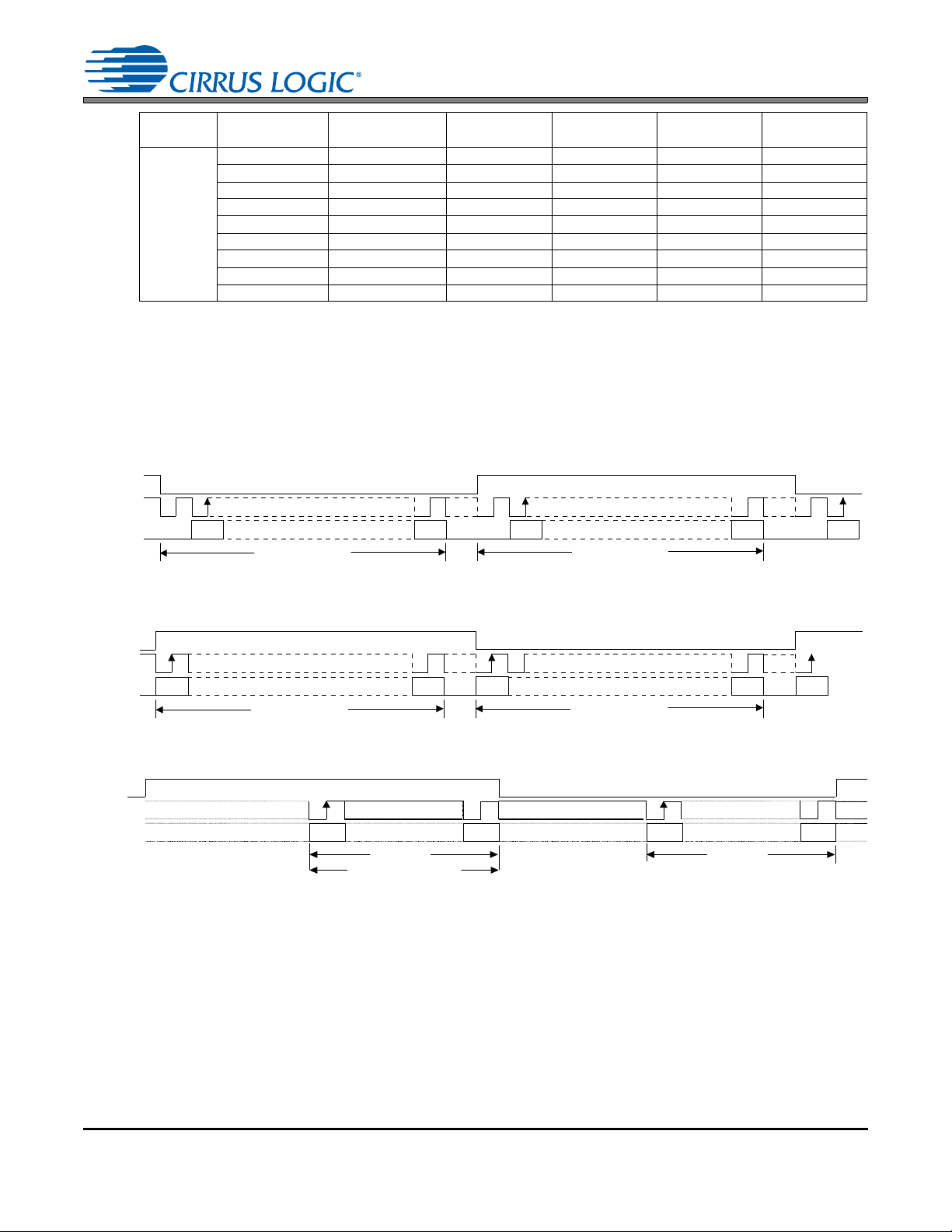
3/1/13
LRCK
SCLK
MSB LSB
MSB
LSB
AOUTA / AINxA
Left C hannel Right C hannel
SDOUT
SDIN
AOUTB / AINxB
MSB
Figure 16. I²S Format
LRCK
SCLK
MSB LSB
MSB
LSB
Left Channel Right Channel
SDOUT
SDIN
MSB
AOUTA / AINxA
AOUTB / AINxB
Figure 17. Left-Justified Format
LRCK
SCLK
MSB LSB
MSB LSB
Left Channel Right Chan nel
SDIN
AOUTL AOUTR
Audio Word Length (AWL)
Figure 18. Right-Justified Format (DAC only)
CS42L52
MCLK
(MHz)
Sample Rate,
Fs (kHz)
SPEED[1:0]
(AUTO=’0’b)
8.0000 11 1 1 01 0
12.0000 11 0 1 01 0
24.0000 10 0 1 01 0
32.0000 01 1 1 01 0
27.0000
44.117601 0 1110
48.0000 01 0 1 01 0
11.029411 0 1110
22.058810 0 1110
16.0000 10 1 1 01 0
4.7 Digital Interface Formats
The serial port operates in standard I²S, Left-justified, Right-justified (DAC only), or DSP Mode digital interface formats with varying bit dep ths from 16 to 24. Data is cloc ked out of t he ADC or into t he DAC on the
rising edge of SCLK.
32kGROUP VIDEOCLK RATIO[1:0] MCLKDIV2
Table 1. MCLK, LRCK Quick Decode
4.7.1 DSP Mode
In DSP Mode, the LRCK acts as a frame sync for 2 data-pac ked words (left and right channel) input on
SDIN and output on SDOUT. The MSB is input/output on the first SCLK rising edge after the frame sync
rising edge. The right channel immediately follows the left channel.
DS680F2 35
Page 36

3/1/13
LRCK
SCLK
MSB LS B
SDIN
HP/LINE OUTB
LSB
Lef t Channel
Right Channel
MSB LSB MSB
Audio Word Length (AWL)
1/fs
HP/LINE OUTA
Figure 19. DSP Mode Format)
CS42L52
When configuring the 16-bit SDOUT word length with an 8 kHz sample rate in master mode and when
SCLK is set equal to MCLK, perform the following write sequences:
Register commands ONLY when entering DSP 16-bit, 8 kHz Fs, SCLK=MCLK, master mode:
Register[Bits] Value Description
1 0x0C[1:0] 0x03 Mute the ADC outputs to ensure no audible artifacts are transmitted when changing modes.
2 Refer to Section 4.10 Follow the recommended power down sequence for the HP and PWM outputs.
3 0x02[0] 0x01 Power down the CODEC.
4 0x05[7:0] 0x72 Enable 8 kHz Fs for MCLK=12.000 MHz.
5 0x06[7:0] 0x93 Enable DSP 16-bit master mode.
6 0x07[6] 0x01 Enable SCLK=MCLK.
7 0x33[6] 0x01 Undisclosed register command for enabling mode mentioned above.
8 Refer to Section 4.9 Follow the recommended power up sequence for the HP and PWM outputs.
9 0x02[0] 0x00 Power up the CODEC.
10 0x0C[1:0] 0x00 Unmute the ADC outputs.
Register commands when exiting DSP 16-bit, 8 kHz Fs, SCLK=MCLK, master mode:
Register[Bits] Value Description
1 0x0C[1:0] 0x03 Mute the ADC outputs to ensure no audible artifacts are transmitted when changing modes.
2 Refer to Section 4.10 Follow the recommended power down sequence for the HP and PWM outputs.
3 0x02[0] 0x01 Power down the CODEC.
4 0x05[7:0] 0x20 Enable 48 kHz Fs for MCLK = 12.2880 MHz or re-establish original settings.
5 0x06[7:0] 0x00 Enable Left-Justified 24-bit slave mode or re-establish original settings.
6 0x07[6] 0x00 Disable SCLK=MCLK or re-establish original settings.
7 0x33[6] 0x00 Undisclosed register command for disabling mode mentioned above.
8 Refer to Section 4.9 Follow the recommended power up sequence for the HP and PWM outputs.
9 0x02[0] 0x00 Power up the CODEC.
10 0x0C[1:0] 0x00 Unmute the ADC outputs.
4.8 Initialization
The CODEC enters a Power-down state on initial power-up. The interpolation and decimation filters, deltasigma and PWM modulators, and control port registers are reset. The internal voltage reference, and
switched-capacitor low-pass filters are powered down.
The device remains in Power-down state until the RESET
once RESET
is high and the desired register settings can be loaded per the descriptions in the Section 6.
Once MCLK is valid, the quiescent voltage, VQ, and the internal voltage reference, FILT+, will begin powering up to normal operation. The charge pump slowly powers up and charges the capacitors. Power is then
applied to the headphone amplifiers and switched-capacitor filters, and the analog/digital outputs enter a muted stat e . Once LRCK is valid, MCLK occurre nces are counted over one LRCK period to de termine the MCLK/LRCK frequency ratio and normal operation begins.
36 DS680F2
pin is brought high. The control port is accessible
Page 37

3/1/13
4.9 Recommended Power-up Sequence
1. Hold RESET low until the power supplies are stable.
2. Bring RESET
3. The default state of the PDN bit is 1. Load the desired register settings while keeping the PDN bit set
to 11.
4. Load the required initialization settings listed in Section 4.11.
5. Apply MCLK at the appropriate frequency, as discussed in Section 4.6. SCLK may be applied or set to
master at any time; LRCK may only be applied or set to master while the PDN bit is set to 1.
6. Set the PDN bit to 0.
7. Bring RESET
prevent power glitch related issues.
4.10 Recommended Power-Down Sequence
To minimize audible pops when turning off or placing the CODEC in standby:
1. Mute the DACs, PWM outputs and ADCs.
2. Disable soft ramp and zero cross volume transitions.
3. Set the PDN bit to 1.
4. Wait at least 100 µs.
The CODEC will be fully powered down after this 100 µs delay. Prior to the removal of the master clock
(MCLK), this delay of at least 100 µs must be implemented after step 3 to avoid premature disruption
of the CODEC’s power down sequence.
high.
low if the analog or digital supplies drop below the recommended operating condition to
CS42L52
A disruption in the CODEC’s power down sequence (i.e. removing the MCLK signal before this 100 µs
delay) has consequences on both the headphone and speaker amplifiers: The charge pump may stop
abruptly, causing the headphone amplifiers to drive the outputs up to the +VHP supply. Also, the last
state of each ‘+’ and ‘-’ PWM output terminal before the premature removal of MCLK could randomly
be held at either VP or AGND. When this event occurs, it is possible for each PWM terminal to output
opposing potentials, creating a DC source into the speaker voice coil.
The disruption of the CODEC’s power down sequence may also cause clicks and pops on the output
of the DACs as the modulator holds the last output level before the MCLK signal was removed.
5. Optionally, MCLK may be removed at this time.
6. To achieve the lowest operating quiescent current, bring RESET
reset to their default state.
7. Power Supply Removal (Option 1): Switch power supplies to a high impedance state.
8. Power Supply Removal (Option 2): To minimize pops when the power supplies are pulled to ground, a
discharge resistor must be added in parallel with the capacitor on the FILT+ pin. With a 1 M resistor
and a 2.2 µF capacitor on FILT+, FILT+ will ramp to ground in approximately 5 seconds. A 1 M resistor
on FILT+ reduces the full scale input/output voltage by approximately 0.25 dB.
After step 5, wait the required time for FILT+ to ramp to ground before pulling VA to ground.
4.11 Required Initialization Settings
The current and thresholds required for various sections in the CODEC must be adjusted by implementing
the initialization settings shown below after power-up sequence step 3. All performance and power consumption measurements were taken with the following settings:
low. All control port registers will be
DS680F2 37
Page 38

1. Write 0x99 to register 0x00.
4 5 6 7 24 25
SCL
CHIP ADDRESS (WRITE) MAP BYTE DATA
DATA +1
START
ACK
STOP
ACKACKACK
1 0 0 1 0 1 AD0 0
SDA
INCR 6 5 4 3 2 1 0 7 6 1 0 7 6 1 0 7 6 1 0
0 1 2 3 8 9 12 16 17 18 19 10 11 13 14 15 27 28
26
DATA +n
Figure 20. Control Port Timing, I²C Write
2. Write 0xBA to register 0x3E.
3. Write 0x80 to register 0x47.
4. Write 1 to bit 7 in register 0x32.
5. Write 00 to bit 7 in register 0x32.
6. Write 0x00 to register 0x00.
4.12 Control Port Operation
The control port is used to access the registers, allowing the CODEC to be configured for the desired operational modes and formats. The operation of the control port may be completely asynchronou s with respect
to the audio sample rates. However, to avoid potential interference problems, the control port pins should
remain static if no operation is required.
The control port operates using an I²C interface with the CODEC acting as a slave device.
4.12.1 I²C Control
SDA is a bidirectional data line. Data is clocked into and out of the device by the clock, SCL. The AD0 pin
sets the LSB of the chip address; ‘0’ when connec ted to DGND, ‘1’ w hen connected to VL. This pin may
be driven by a host controller or directly connected to VL or DGND. The AD0 pin state is sensed and the
LSB of the chip address is set upon the release of the RESET
3/1/13
CS42L52
signal (a low-to-high transition).
The signal timings for a read and write cycle are shown in Figure 20 and Figure 21. A St art condition is
defined as a falling transition of SDA while the clock is high. A Stop condition is defined as a rising transition of SDA while the clock is high. All other transitions of SDA occur while the clock is low. The first byte
sent to the CS42L52 after a Start condition consists of a 7-bit chip address fiel d and a R/W
bit (high for a
read, low for a write).
The upper 6 bits of the address field are fixed at 100101. To communicate with the CS42L52, the chip
address field, which is the first byte sent to the CS42L52, should m atch 100101 follo wed by th e setting of
the AD0 pin. The eighth bit of the address is the R/W
bit. If the operation is a write, the next byte is the
Memory Address Pointer (MAP), which selects the r egister to be read or written. If the opera tion is a read,
the contents of the register pointed to by the MAP will be output. Setting the auto-increment bit in MAP
allows successive reads or writes of consecutive registers. Each byte is separated by an acknowledge
bit. The ACK bit is output from the CS42L52 after each input byte is read and is input to the CS42L52 from
the microcontroller after each transmitted byte.
38 DS680F2
Page 39

3/1/13
SCL
CHIP ADDRESS (WRITE)
MAP BYTE
DATA
DATA +1
START
ACK
STOP
ACK
ACK
ACK
1 0 0 1 0 1 AD0 0
SDA
1 0 0 1 0 1 AD0 1
CHIP ADDRESS (READ)
START
INCR 6 5 4 3 2 1 0
7 0 7 0 7 0
NO
16 8 9 12 13 14 15 4 5 6 7 0 1 20 21 22 23 24
26 27 28
2 3 10 11 17 18 19 25
ACK
DATA + n
STOP
Figure 21. Control Port Timing, I²C Read
CS42L52
Since the read operation cannot set the MAP, an aborted write operation is used as a preamble. As shown
in Figure21, the write operation is aborted after the acknowledge for the MAP byte by sending a stop condition. The following pseudocode illustrates an aborted write operation followed by a read operation.
Send start condition.
Send 10010100 (chip address and write operation).
Receive acknowledge bit.
Send MAP byte, auto-increment off.
Receive acknowledge bit.
Send stop condition, aborting write.
Send start condition.
Send 10010101 (chip address and read operation).
Receive acknowledge bit.
Receive byte, contents of selected register .
Send acknowledge bit.
Send stop condition.
Setting the auto-increment bit in the MAP allows successive reads or writes of consecutive registers. Each
byte is separated by an acknowledge bit.
4.12.2 Memory Address Pointer (MAP)
The MAP byte comes after the address byte and selects the register to be read or written. Refer to the
pseudo code above for implementation details.
4.12.2.1 Map Increment (INCR)
The device has MAP auto-increment capability enabled by the INCR bit (the MSB) of the MAP. If INCR is
set to 0, MAP will stay constant for successive I²C writes or reads. If INCR is set to 1, MAP will auto-increment after each byte is read or written, allowing block reads or writes of successive registers.
DS680F2 39
Page 40

3/1/13
CS42L52
5. REGISTER QUICK REFERENCE
Default values are shown below the bit names. Unless otherwise specified, all “Reserved” bits must maintain their
default values.
Adr. Function 7 6 5 4 3 2 1 0
01h ID CHIPID4 CHIPID3 CHIPID2 CHIPID1 CHIPID0 REVID2 REVID1 REVID0
p42 11100xxx
02h Power Ctl 1 PDN_CHRG Reserved Reserved PDN_PGAB PDN_PGAA PDN_ADCB PDN_ADCA PDN
p42 00000001
03h Power Ctl 2 Reserved Reserved Reserved OVRDB OVRDA PDN_MICB PDN_MICA PDN_BIAS
p43 00000111
04h Power Ctl 3 PDN_HPB1 PDN_HPB0 PDN_HPA1 PDN_HPA0 PDN_SPKB1 PDN_SPKB0 PDN_SPKA1 PDN_SPKA0
p44 00000101
05h Clocking Ctl AUTO SPEED1 SPEED0 32kGROUP VIDEOCLK RATIO1 RATIO0 MCLKDIV2
p44 10100000
06h Interface Ctl 1 M/S
p46 00000000
07h Interface Ctl 2 Reserved SCLK=MCLK DIGLOOP 3ST_SP INV_SWCH BIASLVL2 BIASLVL1 BIASLVL0
p47 00000000
08h Input A Select ADCASEL2 ADCASEL1 ADCASEL0 PGAASEL5 PGAASEL4 PGAASEL3 PGAASEL2 PGAASEL1
p48 10000001
09h Input B Select ADCBSEL2 ADCBSEL1 ADCBSEL0 PGABSEL5 PGABSEL4 PGABSEL3 PGABSEL2 PGABSEL1
p48 10000001
0Ah Analog,
HPF Ctl
p49 10100101
0Bh ADC HPF Cor-
ner Freq.
p50 00000000
0Ch Misc. ADC Ctl ADCB=A DIGMIX DIGSUM1 DIGSUM0 INV_ADCB INV_ADCA ADCBMUTE ADCAMUTE
p50 00000000
0Dh Playback Ctl 1 HPGAIN2 HPGAIN1 HPGAIN0 PLYBCKB=A INV_PCMB INV_PCMA MSTBMUTE MSTAMUTE
p51 01100000
0Eh Misc. Ctl PASSTHRUB PASSTHRUA PASSBMUTE PASSAMUTE FREEZE DEEMPH DIGSFT DIGZC
p52 00000010
0Fh Playback Ctl 2 HPBMUTE HPAMUTE SPKBMUTE SPKAMUTE SPKB=A SPKSWAP SPKMONO MUTE50/50
p54 00000 00
10h MICA Amp Ctl Reserved MICASEL MICACFG MICAGAIN4 MICAGAIN3 MICAGAIN2 MICAGAIN1 MICAGAIN0
p55 00000000
11h MICB Amp Ctl Reserved MICBSEL MICBCFG MICBGAIN4 MICBGAIN3 MICBGAIN2 MICBGAIN1 MICBGAIN0
p55 00000000
12h PGAA Vol, Misc ALCASRDIS ALCAZCDIS PGAAVOL5 PGAAVOL4 PGAAVOL3 PGAAVOL2 PGAAVOL1 PGAAVOL0
p55 00000000
13h PGAB Vol, Misc ALCBSRDIS ALCBZCDIS PGABVOL5 PGABVOL4 PGABVOL3 PGABVOL2 PGABVOL1 PGABVOL0
p55 00000000
14h Passthru A Vol PASSAVOL7 PASSAVOL6 PASSAVOL5 PASSAVOL4 PASSAVOL3 PASSAVOL2 PASSAVOL1 PASSAVOL0
p57 00000000
15h Passthru B Vol PASSBVOL7 PASSBVOL6 PASSBVOL5 PASSBVOL4 PASSBVOL3 PASSBVOL2 PASSBVOL1 PASSBVOL0
p57 00000000
16h ADCA Vol ADCAVOL7 ADCAVOL6 ADCAVOL5 ADCAVOL4 ADCAVOL3 ADCAVOL2 ADCAVOL1 ADCAVOL0
p57 00000000
17h ADCB Vol ADCBVOL7 ADCBVOL6 ADCBVOL5 ADCBVOL4 ADCBVOL3 ADCBVOL2 ADCBVOL1 ADCBVOL0
p57 00000000
18h ADCMIXA Vol AMIXAMUTE AMIXAVOL6 AMIXAVOL5 AMIXAVOL4 AMIXAVOL3 AMIXAVOL2 AMIXAVOL1 AMIXAVOL0
p58 10000000
19h ADCMIXB Vol AMIXBMUTE AMIXBVOL6 AMIXBVOL5 AMIXBVOL4 AMIXBVOL3 AMIXBVOL2 AMIXBVOL1 AMIXBVOL0
p58 10000000
1Ah PCMMIXA Vol PMIXAMUTE PMIXAVOL6 PMIXAVOL5 PMIXAVOL4 PMIXAVOL3 PMIXAVOL2 PMIXAVOL1 PMIXAVOL0
p58 00000000
HPFB HPFRZB HPFA HPFRZA ANLGSFTB ANLGZCB ANLGSFTA ANLGZCA
Reserved Reserved Reserved Reserved HPFB_CF1 HPFB_CF0 HPFA_CF1 HPFA_CF0
INV_SCLK ADCDIF DSP DACDIF1 DACDIF0 AWL1 AWL0
40 DS680F2
Page 41

3/1/13
CS42L52
Adr. Function 7 6 5 4 3 2 1 0
1Bh PCMMIXB Vol PMIXBMUTE PMIXBVOL6 PMIXBVOL5 PMIXBVOL4 PMIXBVOL3 PMIXBVOL2 PMIXBVOL1 PMIXBVOL0
p58 000 0000 0
1Ch BEEP Freq,
On Time
p59 000 0000 0
1Dh BEEP Vol,
Off Time
p60 000 0000 0
1Eh BEEP,
Tone Cfg.
p61 000 0000 0
1Fh Tone Ctl TREB3 TREB2 TREB1 TREB0 BASS3 BASS2 BASS1 BASS0
p62 100 0100 0
20h Master A Vol MSTAVOL7 MSTAVOL6 MSTAVOL5 MSTAVOL4 MSTAVOL3 MSTAVOL2 MSTAVOL1 MSTAVOL0
p63 000 0000 0
21h Master B Vol MSTBVOL7 MSTBVOL6 MSTBVOL5 MSTBVOL4 MSTBVOL3 MSTBVOL2 MSTBVOL1 MSTBVOL0
p63 000 0000 0
22h Headphone A
Volume
p63 000 0000 0
23h Headphone B
Volume
p63 000 0000 0
24h Speaker A
Volume
p64 000 0000 0
25h Speaker B
Volume
p64 000 0000 0
26h Channel Mixer
and Swap
p64 000 0000 0
27h Limit Ctl 1,
Thresholds
p65 000 0000 0
28h Limit Ctl 2,
Release Rate
p66 011 1111 1
29h Limiter Attack
Rate
p67 110 0000 0
2Ah ALC Ctl 1,
Attack Rate
p67 000 0000 0
2Bh ALC Release
Rate
p68 001 1111 1
2Ch ALC Thresh-
olds
p68 000 0000 0
2Dh Noise Gate Ctl NGALL NG NGBOOST THRESH2 THRESH1 THRESH0 NGDELAY1 NGDELAY0
p69 000 0000 0
2Eh Overflow and
Clock Status
p70 000 0000 0
2Fh Battery Com-
pensation
p71 000 0000 0
30h VP Battery
Level
p72 000 0000 0
31h Speaker Status Reserved Reserved SPKASHRT SPKBSHRT SPKR/HP Reserved Reserved Reserved
p72 000 0000 0
32h Reserved Reserved Reserved Reserved Reserved Reserved Reserved Reserved Reserved
33h Reserved Reserved Reserved Reserved Reserved Reserved Reserved Reserved Reserved
34h Charge Pump
Frequency
p73 010 1111 1
FREQ3 FREQ2 FREQ1 FREQ0 ONTIME3 ONTIME2 ONTIME1 ONTIME0
OFFTIME2 OFFTIME1 OFFTIME0 BPVOL4 BPVOL3 BPVOL2 BPVOL1 BPVOL0
BEEP1 BEEP0 BEEPMIXDIS TREB_CF1 TREB_CF0 BASS_CF1 BASS_CF0 TC_EN
HPAVOL7 HPAVOL6 HPAVOL5 HPAVOL4 HPAVOL3 HPAVOL2 HPAVOL1 HPAVOL0
HPBVOL7 HPBVOL6 HPBVOL5 HPBVOL4 HPBVOL3 HPBVOL2 HPBVOL1 HPBVOL0
SPKAVOL7 SPKAVOL6 SPKAVOL5 SPKAVOL4 SPKAVOL3 SPKAVOL2 SPKAVOL1 SPKAVOL0
SPKBVOL7 SPKBVOL6 SPKBVOL5 SPKBVOL4 SPKBVOL3 SPKBVOL2 SPKBVOL1 SPKBVOL0
PCMASWP1 PCMASWP0 PCMBSWP1 PCMBSWP0 ADCASWP1 ADCASWP0 ADCBSWP1 ADCBSWP0
LMAX2 LMAX1 LMAX0 CUSH2 CUSH1 CUSH0 LIMSRDIS LIMZCDIS
LIMIT LIMIT_ALL LIMRRATE5 LIMRRATE4 LIMRRATE3 LIMRRATE2 LIMRRATE1 LIMRRATE0
Reserved Reserved LIMARATE5 LIMARATE4 LIMARATE3 LIMARATE2 LIMARATE1 LIMARATE0
ALCB ALCA ALCARATE5 AALCRATE4 ALCARATE3 ALCARATE2 ALCARATE1 ALCARATE0
Reserved Reserved ALCRRATE5 ALCRRATE4 ALCRRATE3 ALCRRATE2 ALCRRATE1 ALCRRATE0
ALCMAX2 ALCMAX1 ALCMAX0 ALCMIN2 ALCMIN1 ALCMIN0 Reserved Reserved
Reserved SPCLKERR DSPBOVFL DSPAOVFL PCMAOVFL PCMBOVFL ADCAOVFL ADCBOVFL
BATTCMP VPMONITOR Reserved Reserved VPREF3 VPREF2 VPREF1 VPREF0
VPLVL7 VPLVL6 VPLVL5 VPLVL4 VPLVL3 VPLVL2 VPLVL1 VPLVL0
001 1 101 1
000 0 000 0
CHGFREQ3 CHGFREQ2 CHGFREQ1 CHGFREQ0 Reserved Reserved Reserved Reserved
DS680F2 41
Page 42

3/1/13
CS42L52
6. REGISTER DESCRIPTION
All registers are read/write except for the Chip I.D. and Revision Register and Interrupt Status Register, which are
read only. See the following bit definition tables for bit assignment information. The default stat e of ea ch b it afte r a
power-up sequence or reset is listed in each bit description. Unless otherwise specified, all “Reserved” b its must
maintain their default value.
6.1 Chip I.D. and Revision Register (Address 01h) (Read Only)
76543210
CHIPID4 CHIPID3 CHIPID2 CHIPID1 CHIPID0 REVID2 REVID1 REVID0
6.1.1 Chip I.D. (Read Only)
I.D. code for the CS42L52.
CHIPID[4:0] Device
11100 CS42L52
6.1.2 Chip Revision (Read Only)
CS42L52 revision level.
REVID[2:0] Revision Level
000 A0
001 A1
010 B0
011 B1
6.2 Power Control 1 (Address 02h)
76543210
PDN_CHRG Reserved Reserved PDN_PGAB PDN_PGAA PDN_ADCB PDN_ADCA PDN
6.2.1 Power Down ADC Charge Pump
Configures the power state of the ADC charge pump.
PDN_CHRG ADC Charge Pump Status
0 Powered Up
1 Powered Down
6.2.2 Power Down PGAx
Configures the power state of PGA channel x.
PDN_PGAx PGA Status
0 Powered Up (ONLY when the ADC or the analog passthru is used)
1 Powered Down
Application “Analog In to Analog Out Passthrough” on page 31
Notes:
1. The CS42L52 employs a scheme for controlling the power to the PGA when PASSTHRU (“Passthrough
Analog” on page 52) is enabled. Refer to the referenced application for more information.
2. This bit should be used in conjunction with ADCxSEL and PGAxSEL bits to determine the analog
42 DS680F2
Page 43

input path. The PGAxSEL bits may be used to isolate the input signal(s) from the PGA outputs. When
the PGA is powered down, no input should be selected. Refer to “ADC Input Select” on page 48 and
“PGA Input Mapping” on page 49 for the required settings.
6.2.3 Power Down ADCx
Configures the power state of ADC channel x.
PDN_ADCx ADC Status
0 Powered Up
1 Powered Down
Application “Analog In to Analog Out Passthrough” on page 31
Notes:
1. The CS42L52 employs a scheme for controlling the power to the ADC when PASSTHRU
(“Passthrough Analog” on page 52) and PDN_OVRD (“Power Down ADC Override” on page 43) are
enabled. Refer to the referenced application.
6.2.4 Power Down
Configures the power state of the entire CODEC.
PDN CODEC Status
0 Powered Up
1 Powered Down
3/1/13
CS42L52
6.3 Power Control 2 (Address 03h)
76543210
Reserved Reserved Reserved OVRDB OVRDA PDN_MICB PDN_MICA PDN_BIAS
6.3.1 Power Down ADC Override
Configures an override of the power down cont ro l for ADCx.
OVRDx PDN_ADC Override
0 Disable
1 Enable
Application “Analog In to Analog Out Passthrough” on page 31
6.3.2 Power Down MICx
Configures the power state of the microphone pre-amplifier for channel x.
PDN_MICx MIC Pre-Amp Status
0 Powered Up
1 Powered Down
Application “MIC Inputs” on page 26
6.3.3 Power Down MIC Bias
Configures the power state of the microphone bias circuit.
PDN_BIAS MIC Bias Status
0 Powered Up
1 Powered Down
DS680F2 43
Page 44

3/1/13
CS42L52
6.4 Power Control 3 (Address 04h)
76543210
PDN_HPB1 PDN_HPB0 PDN_HPA1 PDN_HPA0 PDN_SPKB1 PDN_SPKB0 PDN_SPKA1 PDN_SPKA0
6.4.1 Headphone Power Control
Configures how the SPKR/HP pin, 31, controls the power for the headphone amplifier.
PDN_HPx[1:0] Headphone Status
00
01
10 Headphone channel is always ON.
11 Headphone channel is always OFF.
6.4.2 Speaker Power Control
Configures how the SPKR/HP pin, 31, controls the power for the speaker amplifier.
PDN_SPKx[1:0] Speaker Status
00
01
10 Speaker channel is always ON.
11 Speaker channel is always OFF.
Headphone channel is ON when the SPKR/HP pin, 31, is LO.
Headphone channel is OFF when the SPKR/HP pin, 31, is HI.
Headphone channel is ON when the SPKR/HP pin, 31, is HI.
Headphone channel is OFF when the SPKR/HP pin, 31, is LO.
Speaker channel is ON when the SPKR/HP pin, 31, is LO.
Speaker channel is OFF when the SPKR/HP pin, 31, is HI.
Speaker channel is ON when the SPKR/HP pin, 31, is HI.
Speaker channel is OFF when the SPKR/HP pin, 31, is LO.
6.5 Clocking Control (Address 05h)
76543210
AUTO SPEED1 SPEED0 32k_GROUP VIDEOCLK RATIO1 RATIO0 MCLKDIV2
6.5.1 Auto-Detect
Configures the auto-detect circuitry for detecting the speed mode of the CODEC when operating as a
slave.
AUTO Auto-detection of Speed Mode
0 Disabled
1 Enabled
Application: “Serial Port Clocking” on page 33
Notes:
1. The SPEED[1:0] bits are ignored and speed is determined by the MCLK/LRCK ratio.
2. Certain sample and MCLK frequencies require setting the SPEED[1:0] bits, the 32k_GROUP bit
(“32kHz Sample Rate Group” on page 45) and/or the VIDEOCLK bit (“27 MHz Video Clock” on
page 45) and RATIO[1:0] bits (“Internal MCLK/LRCK Ratio” on page 45). Low sample rates may also
affect dynamic range performance in the typical audio band. Refer to the referenced application for
more information.
44 DS680F2
Page 45

6.5.2 Speed Mode
Configures the speed mode of the CODEC in slave mode and sets the appropriate MCLK divide ratio for
LRCK and SCLK in master mode.
SPEED[1:0]
00 Double-Speed Mode (DSM - 50 kHz -100 kHz Fs) 128 64
01 Single-Speed Mode (SSM - 4 kHz -50 kHz Fs) 256 64
10 Half-Speed Mode (HSM - 12.5kHz -25 kHz Fs) 512 64
11 Quarter-Speed Mode (QSM - 4 kHz -12.5 kHz Fs)
Application: “Serial Port Clocking” on page 33
Notes:
1. Slave/Master Mode is determined by the M/S
2. Certain sample and MCLK frequencies require setting the SPEED[1:0] bits, the 32k_GROUP bit
(“32kHz Sample Rate Group” on page 45) and/or the VIDEOCLK bit (“27 MHz Video Clock” on
page 45) and RATIO[1:0] bits (“Internal MCLK/LRCK Ratio” on page 45). Low sample rates may also
affect dynamic range performance in the typical audio band. Refer to the referenced application for
more information.
3. These bits are ignored when the AUTO bit (“Auto-Detect” on page 44) is enabled.
3/1/13
CS42L52
Slave Mode Master Mode
Serial Port Speed MCLK/LRCK Ratio SCLK/LRCK Ratio
1024
bit in “Master/Slave Mode” on page 46.
64
6.5.3 32kHz Sample Rate Group
Specifies whether or not the input/output sample rate is 8 kHz, 16 kHz or 32 kHz.
32kGROUP 8 kHz, 16 kHz or 32 kHz sample rate?
0 No
1Yes
Application: “Serial Port Clocking” on page 33
6.5.4 27 MHz Video Clock
Specifies whether or not the external MCLK frequency is 27 MHz
VIDEOCLK 27 MHz MCLK?
0 No
1Yes
Application: “Serial Port Clocking” on page 33
6.5.5 Internal MCLK/LRCK Ratio
Configures the internal MCLK/LRCK ratio.
RATIO[1:0] Internal MCLK Cycles per LRCK SCLK/LRCK Ratio in Master Mode
00 128 64
01 125 62
10 132 66
11 136 68
Application: “Serial Port Clocking” on page 33
DS680F2 45
Page 46

3/1/13
CS42L52
6.5.6 MCLK Divide By 2
Divides the input MCLK by 2 prior to all internal circuitry.
MCLKDIV2 MCLK signal into CODEC
0 No divide
1 Divided by 2
Application: “Serial Port Clocking” on page 33
Note: In slave mode, this bit is ignored when the AUTO bit (“Auto-Detect” on page 44) is disabled.
6.6 Interface Control 1 (Address 06h)
76543210
M/S
6.6.1 Master/Slave Mode
INV_SCLK ADCDIF DSP DACDIF1 DACDIF0 AWL1 AWL0
Configures the serial port I/O clocking.
M/S Serial Port Clocks
0 Slave (input ONLY)
1 Master (output ONLY)
6.6.2 SCLK Polarity
Configures the polarity of the SCLK signal.
INV_SCLK SCLK Polarity
0 Not Inverted
1 Inverted
6.6.3 ADC Interface Format
Configures the digital interface format for data on SDOUT.
ADCDIF ADC Interface Format
0 Left Justified
1I²S
Application: “Digital Interface Formats” on page 35
6.6.4 DSP Mode
Configures a data-packed interface format for both the ADC and DAC.
DSP DSP Mode
0 Disabled
1 Enabled
Application: “DSP Mode” on page 35
Notes:
1. Select the audio word length using the AWL[1:0] bits (“Audio Word Length” on page 47).
2. The interface format for both the ADC and the DAC must be set to “Left-Justified” when DSP Mode
is enabled.
46 DS680F2
Page 47

6.6.5 DAC Interface Format
Configures the digital interface format for data on SDIN.
DACDIF[1:0] DAC Interface Format
00 Left Justified, up to 24-bit data
01 I²S, up to 24-bit data
10 Right Justified
11 Reserved
Application: “Digital Interface Formats” on page 35
Note: Select the audio word length for Right Justified using the AWL[1:0] bits (“Audio Word Length” on
page 47).
6.6.6 Audio Word Length
Configures the audio sample word length used for the data into SDIN and out of SDOUT.
AWL[1:0]
00 32-bit data 24-bit data
01 24-bit data 20-bit data
10 20-bit data 18-bit data
11 16-bit data 16-bit data
Application: “DSP Mode” on page 35
Audio Word Length
DSP Mode Right Justified (DAC ONLY)
3/1/13
CS42L52
Note: When the internal MCLK/LRCK ratio is set to 125 in master mode, the 32-bit data width option
for DSP Mode is not valid unless SCLK=MCLK.
6.7 Interface Control 2 (Address 07h)
765432 10
Reserved SCLK=MCLK DIGLOOP 3ST_SP INV_SWCH BIASLVL2 BIASLVL1 BIASLVL0
6.7.1 SCLK equals MCLK
Configures the SCLK signal source for master mode.
SCLK=MCLK Output SCLK
0 Re-timed signal, synchronously derived from MCLK
1 Non-retimed, MCLK signal
Note: This bit is only valid for MCLK = 12.0000 MHz.
6.7.2 SDOUT to SDIN Digital Loopback
Configures an internal loops the signal on the SDOUT pin to SDIN.
DIGLOOP Internal Loopback
0 Disabled; SDOUT internally disconnected from SDIN
1 Enabled; SDOUT internally connected to SDIN
DS680F2 47
Page 48

6.7.3 Tri-State Serial Port Interface
Determines the state of the serial port drivers.
3ST_SP
0 Serial Port clocks are inputs and SDOUT is output Serial Port clocks and SDOUT are outputs
1 Serial Port clocks are inputs and SDOUT is HI-Z Serial Port clocks and SDOUT are HI-Z
Serial Port Status
Slave Mode Master Mode
Notes:
1. Slave/Master Mode is determined by the M/S
2. When the serial port is tri-stated in master mode, the ADC and DAC serial ports are clocked internally.
6.7.4 Speaker/Headphone Switch Invert
Determines the control signal polarity of the SPK/HP_SW pin.
INV_SWCH SPK/HP_SW pin 6 Control
0 Not inverted
1 Inverted
3/1/13
CS42L52
bit in “Master/Slave Mode” on page 46.
6.7.5 MIC Bias Level
Sets the output voltage level on the MICBIAS output pin.
BIASLVL[2:0] Output Bias Level
000 0.5 x VA
001 0.6 x VA
010 0.7 x VA
011 0.8 x VA
100 0.83 x VA
101 0.91 x VA
110 Reserved
111 Reserved
6.8 Input x Select: ADCA and PGAA (Address 08h), ADCB and PGAB (Address 09h)
7 6 5 4 3210
ADCASEL2 ADCASEL1 ADCASEL0 PGAASEL5 PGAASEL4 PGAASEL3 PGAASEL2 PGAASEL1
6.8.1 ADC Input Select
Selects the specified analog input signal into ADCx.
ADCxSEL[2:0] Selected Input to ADCx
000 AIN1x
001 AIN2x
010 AIN3x
011 AIN4x
100 PGAx - Use PGAxSEL bits (“PGA Input Mapping” on page 49) to select input channels
101 Reserved
110 Reserved
111 Reserved
Application: “Analog Inputs” on page 25
48 DS680F2
Page 49

3/1/13
CS42L52
6.8.2 PGA Input Mapping
Selects one or sums/mixes the analog input signal into the PGA. Each bit of the PGAx_SEL[5:1] word
corresponds to individual channels (i.e. PGAx_SEL1 selects AIN1x, PGAx_SEL2 selects AIN2x, etc.).
PGAxSEL[5:1] Selected Input to PGAx (Examples)
00000 No inputs selected
00001 AIN1x
00010 AIN2x
00100 AIN3x
01000 AIN4x
for single-ended MIC inputs, use MICxSEL (“MIC x Select” on page 55) to select MIC 1 or MIC 2; for
10000
10001 MICx + AIN1x
10011 MICx + AIN1x + AIN2x
Application: “Analog Inputs” on page 25
Note: Table does not show all possible combinations.
6.9 Analog and HPF Control (Address 0Ah)
76543210
HPFB HPFRZB HPFA HPFRZA ANLGSFTB ANLGZCB ANLGSFTA ANLGZCA
MICx;
differential MIC inputs, enable MICxCFG (
“MICx Configuration” on page 55)
6.9.1 ADCx High-Pass Filter
Configures the internal high-pass filter after ADCx.
HPFx High Pass Filter Status
0 Disabled
1 Enabled
6.9.2 ADCx High-Pass Filter Freeze
Configures the high pass filter’s digital DC subtraction and/or calibration after ADCx.
HPFRZx High Pass Filter Digital Subtraction
0 Continuous DC Subtraction
1 Frozen DC Subtraction
6.9.3 Ch. x Analog Soft Ramp
Configures an incremental volume ramp from the current level to the new level at the specified rate.
ANLGSFTx Volume Changes Affected Analog Volume Controls
0 Do not occur with a soft ramp
1 Occur with a soft ramp
Ramp Rate: 1/2 dB every 16 LRCK cycles
6.9.4 Ch. x Analog Zero Cross
Configures when the signal level changes occur for the analog volume controls.
ANLGZCx Volume Changes Affected Analog Volume Controls
0
1 Occur on a zero crossing
Do not occur on a zero crossing
MICxGAIN[4:0] (“MICx Gain” on page 55), PGAxVOL[5:0] (“PGAx Volume”
on page 56), and PASSxVOL[7:0] (“Passthrough x Volume” on page 57)
MICxGAIN[4:0] (“MICx Gain” on page 55), PGAxVOL[5:0] (“PGAx Volume”
on page 56), and PASSxVOL[7:0] (“Passthrough x Volume” on page 57)
Note: If the signal does not encounter a zero crossing, the requested volume change will occur after a
timeout period of 1024 sample periods (approximately 10.7 ms at 48 kHz sample rate).
DS680F2 49
Page 50
3/1/13
CS42L52
6.10 ADC HPF Corner Frequency (Address 0Bh)
76543210
Reserved Reserved Reserved Reserved HPFB_CF1 HPFB_CF0 HPFA_CF1 HPFA_CF0
6.10.1 HPF x Corner Frequency
Sets the corner frequency (-3 dB point) for the internal High-Pass Filter (HPF).
HPFx_CF[1:0] HPF Corner Frequency Setting (Fs=48 kHz)
00 Normal setting as specified in “ADC Digital Filter Characteristics” on page 14
01 119 Hz
10 236 Hz
11 464 Hz
6.11 Misc. ADC Control (Address 0Ch)
76543210
ADCB=A DIGMUX DIGSUM1 DIGSUM0 INV_ADCB INV_ADCA ADCBMUTE ADCAMUTE
6.11.1 Analog Front-End Volume Setting B=A
Configures independent or ganged volume control and muting of the analog front end.
ADCB=A Single Volume Control Affected Volume Controls
0 Disabled ADCxVOL[7:0] (“ADCx Volume” on page 57),
1 Enabled
6.11.2 Digital MUX
Selects the signal source for the ADC serial port
DIGMUX SDOUT Signal Source
0 ADC
1DSP
6.11.3 Digital Sum
Configures a mix/swap of ADCA and ADCB.
DIGSUM[1:0]
00 ADCA ADCB
01 (ADCA + ADCB)/2 (ADCA + ADCB)/2
10 (ADCA - ADCB)/2 (ADCA - ADCB)/2
11 ADCB ADCA
ADCxMUTE (“ADC Mute” on page 51),
ALC and Limiter Attack/Release (page 66 to page 68)
MICxGAIN[4:0] (“MICx Gain” on page 55),
PGAxVOL[5:0] (“PGAx Volume” on page 56),
PASSxVOL[7:0] (“Passthrough x Volume” on page 57)
Serial Output Signal
Left Channel Right Channel
50 DS680F2
Page 51

3/1/13
CS42L52
6.11.4 Invert ADC Signal Polarity
Configures the polarity of the ADC signal.
INV_ADCx ADC Signal Polarity
0 Not Inverted
1 Inverted
6.11.5 ADC Mute
Configures a digital mute on ADC channel x.
ADCxMUTE ADC Mute
0 Disabled
1 Enabled
Note: When the ADCxMUTE bit is enabled, the PGA will automatically apply 6 dB of attenuation.
6.12 Playback Control 1 (Address 0Dh)
76543210
HPGAIN2 HPGAIN1 HPGAIN0 PLYBCKB=A INV_PCMB INV_PCMA MSTBMUTE MSTAMUTE
6.12.1 Headphone Analog Gain
Selects the gain multiplier for the headphone/line outputs.
HPGAIN[2:0] Headphone/Line Gain Setting (G)
000 0.3959
001 0.4571
010 0.5111
011 0.6047
100 0.7099
101 0.8399
110 1.000
111 1.1430
Note: Refer to “Line Output Voltage Level Characteristics” on page 19 and “Headphone Output Power
Characteristics” on page 18.
6.12.2 Playback Volume Setting B=A
Configures independent or ganged volume control of all playback channels.
PLYBCKB=A Single Volume Control Affected Volume Controls
0 Disabled HPxMUTE (“Playback Control 2 (Address 0Fh)” on page 54),
1 Enabled
AMIXxVOL[7:0] (“ADC Mixer Channel x Volume” on page 58),
PMIXxVOL[7:0] (“PCM Mixer Channel x Volume” on page 58),
MSTxVOL[7:0] (“Master Volume Control” on page 63),
HPxVOL[7:0] (“Headphone Volume Control” on page 63)
DS680F2 51
Page 52

3/1/13
CS42L52
6.12.3 Invert PCM Signal Polarity
Configures the polarity of the digital input signal.
INV_PCMx PCM Signal Polarity
0 Not Inverted
1 Inverted
6.12.4 Master Playback Mute
Configures a digital mute on the master volume control for channel x.
MSTxMUTE Master Mute
0 Not Inverted
1 Inverted
Note: The muting function is affected by the DIGSFT (“Digital Soft Ramp” on page 53) and DIGZC
(“Digital Zero Cross” on page 53) bits.
6.13 Miscellaneous Controls (Address 0Eh)
76543210
PASSTHRUB PASSTHRUA PASSBMUTE PASSAMUTE FREEZE DEEMPH DIGSFT DIGZC
6.13.1 Passthrough Analog
Configures an analog passthrough from the PGA inputs to the headphone/line outputs.
PASSTHRUx Analog In Routed to HP/Line Output
0 Disabled
1 Enabled
Notes:
1. The Passthrough volume control is realized using a combination of the PGA volume control settings
(“PGAx Volume” on page 56) and the headphone amplifier volume control settings (hidden). When
passthrough is enabled and the PGA to ADC path is selected, the signal seen by the ADC will change
depending on the passthrough volume setting.
6.13.2 Passthrough Mute
Configures an analog mute on the channel x analog in to analog out passthrough.
PASSxMUTE Passthrough Mute
0 Disabled
1 Enabled
6.13.3 Freeze Registers
Configures a hold on all register settings.
FREEZE Control Port Status
0 Register changes take effect immediately
1
Modifications may be made to all control port registers without the changes taking effect until after the
FREEZE is disabled.
Notes:
1. Use this bit only to synchronize run-time controls, such as volume and mute, during normal operation .
52 DS680F2
Page 53
Using this bit before the relevant circuitry begins normal operation could cause the change to take
effect immediately, ignoring the FREEZE bit.
6.13.4 HP/Speaker De-emphasis
Configures a 15s/50s digital de-emphasis filter response on the headphone/line and speaker outputs .
DEEMPHASIS Control Port Status
0 Disabled
1 Enabled
6.13.5 Digital Soft Ramp
Configures an incremental volume ramp from the current level to the new level at the specified rate.
DIGSFT Volume Changes Affected Digital Volume Controls
0 Do not occur with a soft ramp MSTxMUTE (“Master Playback Mute” on page 52),
1 Occur with a soft ramp
Ramp Rate: 1/8 dB every LRCK cycle
3/1/13
CS42L52
HPxMUTE, SPKxMUTE (“Playback Control 2 (Address 0Fh)” on page 54),
ADCxVOL[7:0] (“ADCx Volume” on page 57),
AMIXxMUTE, AMIXxVOL[7:0] (“ADC Mixer Channel x Volume” on page 58),
PMIXxMUTE, PMIXxVOL[7:0] (“PCM Mixer Channel x Volume” on page 58),
MSTxVOL[7:0] (“Master Volume Control” on page 63),
HPxVOL[7:0] (“Headphone Volume Control” on page 63),
SPKxVOL[7:0] (“Speaker Volume Control” on page 64),
ALC and Limiter Attack/Release (page 66 to page 68)
Beep Volume (“Beep Volume” on page 61)
Note: When the DIGSFT bit is enabled, the Master Volume (MSTxVOL[7:0]) transitions are guaranteed
to occur with a soft ramp only when
6.13.6 Digital Zero Cross
Configures when the signal level changes occur for the digital volume controls.
DIGZC Volume Changes Affected Digital Volume Controls
0
1 Occur on a zero crossing
Notes:
1. If the signal does not encounter a zero crossing, the requested volume change will occur after a
timeout period between 1024 and 2048 sa mple pe riods (21.3 ms to 42.7 ms at 4 8 kHz sample r ate).
2. The zero cross function is independently monitored and implemented for each channel.
3. The DIS_LIMSFT bit (“Limiter Soft Ramp Disable” on page 65) is ignored when zero cross is enabled.
4. Wh en the DIGZ C bit is en abled , th e Ma st er Volume (MSTxVOL[7:0]) transitions are guaranteed to
occur on a zero cross only if bits 7 and 6 in register 29h are set to '00'b
Do not occur on a zero crossing
bits 7 and 6 in register 29h are set to ‘00’b.
MSTxMUTE (“Master Playback Mute” on page 52),
AMIXxMUTE, AMIXxVOL[7:0] (“ADC Mixer Channel x Volume” on page 58),
PMIXxMUTE, PMIXxVOL[7:0] (“PCM Mixer Channel x Volume” on page 58),
MSTxVOL[7:0] (“Master Volume Control” on page 63),
ALC and Limiter Attack/Release (page 66 to page 68)
Beep Volume (“Beep Volume” on page 61)
DS680F2 53
Page 54
3/1/13
CS42L52
6.14 Playback Control 2 (Address 0Fh)
76543210
HPBMUTE HPAMUTE SPKBMUTE SPKAMUTE SPKB=A SPKSWAP SPKMONO MUTE50/50
6.14.1 Headphone Mute
Configures a digital mute on headphone channel x.
HPxMUTE Headphone Mute
0 Disabled
1 Enabled
6.14.2 Speaker Mute
Configures a digital mute on speaker channel x.
SPKxMUTE Speaker Mute
0 Disabled
1 Enabled
6.14.3 Speaker Volume Setting B=A
Configures independent or ganged volume control of the speaker output.
SPKB=A Single Volume Control Affected Volume Controls
0 Disabled
1 Enabled
6.14.4 Speaker Channel Swap
Configures a channel swap on the speaker channels.
SPKSWAP Speaker Output
0 Channel A
1 Channel B
Application: “Mono Speaker Output Configuration” on page 32
6.14.5 Speaker MONO Control
Configures a parallel full-bridge output for the speaker channels.
SPKMONO Parallel Full Bridge Output
0 Disabled
1 Enabled
Application: “Mono Speaker Output Configuration” on page 32
6.14.6 Speaker Mute 50/50 Control
SPKxMUTE (“Speaker Mute” on page 54),
SPKxVOL[7:0] (“Speaker Volume Control” on page 64)
Configures how the speaker channels mute.
MUTE50/50 Speaker Mute 50/50
0 Disabled; The PWM amplifiers outputs modulated silence when SPKxMUTE is enabled.
1
Enabled; The PWM amplifiers switch at an exact 50%-duty-cycle signal (not modulated) when SPKxMUTE is
enabled.
54 DS680F2
Page 55

3/1/13
CS42L52
6.15 MICx Amp Control:MIC A (Address 10h) and MIC B (Address 11h)
76543210
Reserved MICxSEL MICxCFG MICxGAIN4 MICxGAIN3 MICxGAIN2 MICxGAIN1 MICxGAIN0
6.15.1 MIC x Select
Selects one of two single-ended MIC inputs on channel x.
MICxSEL MIC x Selection
0 MIC 1x
1 MIC 2x
Application: “MIC Inputs” on page 26
6.15.2 MICx Configuration
Configures the input topology for MICx.
MICxCFG MIC Input Topology
0 Single-Ended
1 Differential
Application: “MIC Inputs” on page 26
6.15.3 MICx Gain
Sets the gain of the microphone pre-amplifier.
MICxGAIN[4:0] Gain
1 1111 32 dB
... ...
1 0000 32 dB
0 1111 30.5 dB
0 1110 30 dB
... ...
0 0000 16 dB
Step Size: 1 dB (unless otherwise noted)
Application: “MIC Inputs” on page 26
6.16 PGAx Vol. and ALCx Transition Ctl.: ALC, PGA A (Address 12h) and ALC, PGA B (Address 13h)
76543210
ALCxSRDIS ALCxZCDIS PGAxVOL5 PGAxVOL4 PGAxVOL3 PGAxVOL2 PGAxVOL1 PGAxVOL0
6.16.1 ALCx Soft Ramp Disable
Configures an override of the analog soft ram p se ttin g.
ALCxSRDIS ALC Soft Ramp Disable
0 OFF; ALC Attack Rate is dictated by the ANLGSFT (“Ch. x Analog Soft Ramp” on page 49) setting
1 ON; ALC volume changes take effect in one step, regardless of the ANLGSFT setting.
Application: “Automatic Level Control (ALC)” on page 26
DS680F2 55
Page 56

6.16.2 ALCx Zero Cross Disable
Configures an override of the analog zero cross setting.
ALCxZCDIS ALC Zero Cross Disable
0 OFF; ALC Attack Rate is dictated by the ANLGZC (“Ch. x Analog Zero Cross” on page 49) setting
1 ON; ALC volume changes take effect at any time, regardless of the ANLGZC setting.
Application: “Automatic Level Control (ALC)” on page 26
6.16.3 PGAx Volume
Sets the volume/gain of the Programmable Gain Amplifier (PGA).
PGAxVOL[5:0] Volume
01 1111 12 dB
... ...
01 1000 12 dB
... ...
00 0001 +0.5 dB
00 0000 0 dB
11 1111 -0.5 dB
... ...
10 1000 -6.0 dB
... ...
10 0000 -6.0 dB
Step Size: 0.5 dB
3/1/13
CS42L52
Note: The PGAxVOL bits are ignored when the PASSTHRUx bit (“Passthrough Analog” on page 52) is
enabled.
56 DS680F2
Page 57

3/1/13
CS42L52
6.17 Passthrough x Volume: PASSAVOL (Address 14h) and PASSBVOL (Address 15h)
76543210
PASSxVOL7 PASSxVOL6 PASSxVOL5 PASSxVOL4 PASSxVOL3 PASSxVOL2 PASSxVOL1 PASSxVOL0
6.17.1 Passthrough x Volume
Sets the volume/gain of the signal routed from the PGA to the headphone/line output.
PASSxVOL[7:0] Gain
0111 1111 12 dB
... ...
0001 1000 12 dB
... ...
0000 0001 +0.5 dB
0000 0000 0 dB
11111 1111 -0.5 dB
... ...
1000 1000 -60.0 dB
... ...
1000 0000 -60.0 dB
Step Size: 0.5 dB (approximate)
Application: “Analog In to Analog Out Passthrough” on page 31
Notes:
1. This register is ignored when the PASSTHRUx bit (“Passthrough Analog” on page 52) is disabled.
2. The step size may deviate from 0.5 dB at settings below -40 dB. Code settings 0x95, 0xA1, 0xAD,
and 0xB9 are not guaranteed to be monotonic.
6.18 ADCx Volume Control: ADCAVOL (Address 16h) and ADCBVOL (Address 17h)
76543210
ADCAVOL7 ADCAVOL6 ADCAVOL5 ADCAVOL4 ADCAVOL3 ADCAVOL2 ADCAVOL1 ADCAVOL0
6.18.1 ADCx Volume
Sets the volume of the ADC signal out the serial data output (SDOUT).
ADCxVOL[7:0] Volume
0111 1111 24 dB
... ...
0001 1000 24 dB
... ...
0000 0000 0 dB
1111 1111 -1.0 dB
1111 1110 -2.0 dB
... ...
1010 0000 -96.0 dB
... ...
1000 0000 -96.0 dB
Step Size: 1.0 dB
DS680F2 57
Page 58

3/1/13
CS42L52
6.19 ADCx Mixer Volume: ADCA (Address 18h) and ADCB (Address 19h)
76543210
AMIXxMUTE AMIXxVOL6 AMIXxVOL5 AMIXxVOL4 AMIXxVOL3 AMIXxVOL2 AMIXxVOL1 AMIXxVOL0
6.19.1 ADC Mixer Channel x Mute
Configures a digital mute on the ADC mix in the DSP.
AMIXxMUTE ADC Mixer Mute
0 Disabled
1 Enabled
6.19.2 ADC Mixer Channel x Volume
Sets the volume/gain of the ADC mix in the DSP.
AMIXxVOL[6:0] Volume
001 1000 +12.0 dB
... ...
000 0001 +0.5 dB
000 0000 0 dB
111 1111 -0.5 dB
... ...
001 1001 -51.5 dB
Step Size: 0.5 dB
6.20 PCMx Mixer Volume: PCMA (Address 1Ah) and PCMB (Address 1Bh)
76543210
PMIXxMUTE PMIXxVOL6 PMIXxVOL5 PMIXxVOL4 PMIXxVOL3 PMIXxVOL2 PMIXxVOL1 PMIXxVOL0
6.20.1 PCM Mixer Channel x Mute
Configures a digital mute on the PCM mix from the serial data input (SDIN) to the DSP.
PMIXxMUTE PCM Mixer Mute
0 Disabled
1 Enabled
6.20.2 PCM Mixer Channel x Volume
Sets the volume/gain of the PCM mix from the serial data input (SDIN) to the DSP.
PMIXxVOL[6:0] Volume
001 1000 +12.0 dB
... ...
000 0001 +0.5 dB
000 0000 0 dB
111 1111 -0.5 dB
... ...
001 1001 -51.5 dB
Step Size: 0.5 dB
58 DS680F2
Page 59

3/1/13
CS42L52
6.21 Beep Frequency and On Time (Address 1Ch)
76543210
FREQ3 FREQ2 FREQ1 FREQ0 ONTIME3 ONTIME2 ONTIME1 ONTIME0
6.21.1 Beep Frequency
Sets the frequency of the beep signal.
FREQ[3:0] Frequency (Fs = 12, 24, 48 or 96 kHz) Pitch
0000 260.87 Hz C4
0001 521.74 Hz C5
0010 585.37 Hz D5
0011 666.67 Hz E5
0100 705.88 Hz F5
0101 774.19 Hz G5
0110 888.89 Hz A5
0111 1000.00 Hz B5
1000 1043.48 Hz C6
1001 1200.00 Hz D6
1010 1333.33 Hz E6
1011 1411.76 Hz F6
1100 1600.00 Hz G6
1101 1714.29 Hz A6
1110 2000.00 Hz B6
1111 2181.82 Hz C7
Application: “Beep Generator” on page 29
Notes:
1. This setting must not change when BEEP is enabled.
2. Beep frequency will scale directly with sample rate, Fs, but is fixed at the nominal Fs within each
speed mode.
DS680F2 59
Page 60

6.21.2 Beep On Time
Sets the on duration of the beep signal.
ONTIME[3:0] On Time (Fs = 12, 24, 48 or 96 kHz)
0000 ~86 ms
0001 ~430 ms
0010 ~780 ms
0011 ~1.20 s
0100 ~1.50 s
0101 ~1.80 s
0110 ~2.20 s
0111 ~2.50 s
1000 ~2.80 s
1001 ~3.20 s
1010 ~3.50 s
1011 ~3.80 s
1100 ~4.20 s
1101 ~4.50 s
1110 ~4.80 s
1111 ~5.20 s
Application: “Beep Generator” on page 29
3/1/13
CS42L52
Notes:
1. This setting must not change when BEEP is enabled.
2. Beep on time will scale inversely with sample rate, Fs, but is fixed at the nominal Fs within each speed
mode.
6.22 Beep Volume and Off Time (Address 1Dh)
76543210
OFFTIME2 OFFTIME1 OFFTIME0 BPVOL4 BPVOL3 BPVOL2 BPVOL1 BPVOL0
6.22.1 Beep Off Time
Sets the off duration of the beep signal.
OFFTIME[2:0] Off Time (Fs = 48 or 96 kHz)
000 ~1.23 s
001 ~2.58 s
010 ~3.90 s
011 ~5.20 s
100 ~6.60 s
101 ~8.05 s
110 ~9.35 s
111 ~10.80 s
Application: “Beep Generator” on page 29
Notes:
1. This setting must not change when BEEP is enabled.
2. Beep off time will scale inversely with sample rate, Fs, but is fixed at the nominal Fs within each speed
mode.
60 DS680F2
Page 61

3/1/13
CS42L52
6.22.2 Beep Volume
Sets the volume of the beep signal.
BEEPVOL[4:0] Gain
00110 +6.0 dB
··· ···
00000 -6 dB
11111 -8 dB
11110 -10 dB
··· ···
00111 -56 dB
Step Size: 2 dB
Application: “Beep Generator” on page 29
Note: This setting must not change when BEEP is enabled.
6.23 Beep and Tone Configuration (Address 1Eh)
76543210
BEEP1 BEEP0 BEEPMIXDIS TREBCF1 TREBCF0 BASSCF1 BASSCF0 TCEN
6.23.1 Beep Configuration
Configures a beep mixed with the HP/Line and SPK output.
BEEP[1:0] Beep Occurrence
00 Off
01 Single
10 Multiple
11 Continuous
Application: “Beep Generator” on page 29
Notes:
1. When used in analog pass-through mode, the output alternates between the signal from the PGA and
the beep signal. The beep signal does not mix with the analog signal from the PGA.
2. Re-engaging the beep before it has completed its initial cycle will cause the beep signal to remain ON
for the maximum ONTIME duration.
6.23.2 Beep Mix Disable
Configures how the beep mixes with the serial data input.
BEEPMIXDIS Beep Output to HP/Line and Speaker
0 Mix Enabled; The beep signal mixes with the digital signal from the serial data input.
1
Application: “Beep Generator” on page 29
Mix Disabled; The output alternates between the signal from the serial data input and the beep signal. The
beep signal does not mix with the digital signal from the serial data input.
Note: This setting must not change when BEEP is enabled.
DS680F2 61
Page 62

6.23.3 Treble Corner Frequency
Sets the corner frequency (-3 dB point) for the treble shelving filter.
TREBCF[1:0] Treble Corner Frequency Setting
00 5 kHz
01 7 kHz
10 10 kHz
11 15 kHz
6.23.4 Bass Corner Frequency
Sets the corner frequency (-3 dB point) for the bass shelving filter.
BASSCF[1:0] Bass Corner Frequency Setting
00 50 Hz
01 100 Hz
10 200 Hz
11 250 Hz
6.23.5 Tone Control Enable
3/1/13
CS42L52
Configures the treble and bass activation.
TCEN Bass and Treble Control
0 Disabled
1 Enabled
Application: “Beep Generator” on page 29
6.24 Tone Control (Address 1Fh)
76543210
TREB3 TREB2 TREB1 TREB0 BASS3 BASS2 BASS1 BASS0
6.24.1 Treble Gain
Sets the gain of the treble shelving filter.
TREB[3:0] Gain Setting
0000 +12.0 dB
··· ···
0111 +1.5 dB
1000 0 dB
1001 -1.5 dB
··· ···
1111 -10.5 dB
Step Size: 1.5 dB
62 DS680F2
Page 63
3/1/13
CS42L52
6.24.2 Bass Gain
Sets the gain of the bass shelving filter.
TREB[3:0] Gain Setting
0000 +12.0 dB
··· ···
0111 +1.5 dB
1000 0 dB
1001 -1.5 dB
··· ···
1111 -10.5 dB
Step Size: 1.5 dB
6.25 Master Volume Control: MSTA (Address 20h) and MSTB (Address 21h)
76543210
MSTxVOL7 MSTxVOL6 MSTxVOL5 MSTxVOL4 MSTxVOL3 MSTxVOL2 MSTxVOL1 MSTxVOL0
6.25.1 Master Volume Control
Sets the volume of the signal out the DSP.
MSTxVOL[7:0] Master Volume
0001 1000 +12.0 dB
··· ···
0000 0000 0 dB
1111 1111 -0.5 dB
1111 1110 -1.0 dB
··· ···
0011 0100 -102 dB
··· ···
0001 1001 -102 dB
Step Size: 0.5 dB
6.26 Headphone Volume Control: HPA (Address 22h) and HPB (Address 23h)
76543210
HPxVOL7 HPxVOL6 HPxVOL5 HPxVOL4 HPxVOL3 HPxVOL2 HPxVOL1 HPxVOL0
6.26.1 Headphone Volume Control
Sets the volume of the signal out the DAC.
HPxVOL[7:0] Headphone Volume
0000 0000 0 dB
1111 1111 -0.5 dB
1111 1110 -1.0 dB
··· ···
0011 0100 -96.0 dB
··· ···
0000 0001 Muted
Step Size: 0.5 dB
DS680F2 63
Page 64

3/1/13
CS42L52
6.27 Speaker Volume Control: SPKA (Address 24h) and SPKB (Address 25h)
76543210
SPKxVOL7 SPKxVOL6 SPKxVOL5 SPKxVOL4 SPKxVOL3 SPKxVOL2 SPKxVOL1 SPKxVOL0
6.27.1 Speaker Volume Control
Sets the volume of the signal out the PWM modulator.
SPKxVOL[7:0] Speaker Volume
0000 0000 0 dB
1111 1111 -0.5 dB
1111 1110 -1.0 dB
··· ···
0100 0000 -96.0 dB
··· ···
0000 0001 Muted
Step Size: 0.5 dB
Note: The maximum step size error is ±0.15 dB.
6.28 ADC and PCM Channel Mixer (Address 26h)
76543210
PCMASWP1 PCMASWP0 PCMBSWP1 PCMBSWP0 ADCASWP1 ADCASWP0 ADCBSWP1 ADCBSWP0
6.28.1 PCM Mix Channel Swap
Configures a mix/swap of the PCM Mix to the headphone/line or speaker outputs.
PCMxSWP[1:0] PCM Mix to HP/LINEOUTA PCM Mix to HP/LINEOUTB
00 Left Right
01
10
11 Right Left
(Left + Right)/2 (Left + Right)/2
6.28.2 ADC Mix Channel Swap
Configures a mix/swap of the ADC Mix to the headphone/line or speaker outputs.
ADCxSWP[1:0] ADC Mix to HP/LINEOUTA Channel ADC Mix to HP/LINEOUTB Channel
00 Left Right
01
10
11 Right Left
(Left + Right)/2 (Left + Right)/2
64 DS680F2
Page 65

3/1/13
CS42L52
6.29 Limiter Control 1, Min/Max Thresholds (Address 27h)
76543210
LMAX2 LMAX1 LMAX0 CUSH2 CUSH1 CUSH0 LIMSRDIS LIMZCDIS
6.29.1 Limiter Maximum Threshold
Sets the maximum level, below full scale, at which to limit and attenuate the output signal at the attack
rate (LIMARATE - “Limiter Release Rate” on page 66).
LMAX[2:0] Threshold Setting
000 0 dB
001 -3 dB
010 -6 dB
011 -9 dB
100 -12 dB
101 -18 dB
110 -24 dB
111 -30 dB
Application: “Limiter” on page 30
Note: Bass, Treble, and digital gain settings that boost the signal beyond the maximu m thresho ld may
trigger an attack.
6.29.2 Limiter Cushion Threshold
Sets the minimum level at which to disengage the Limiter’s attenuation at the release rate (LIMRRATE -
“Limiter Release Rate” on page 66) until levels lie between the LMAX and CUSH thresholds.
CUSH[2:0] Threshold Setting
000 0 dB
001 -3 dB
010 -6 dB
011 -9 dB
100 -12 dB
101 -18 dB
110 -24 dB
111 -30 dB
Application: “Limiter” on page 30
Note: This setting is usually set slightly below the LMAX th re sh old .
6.29.3 Limiter Soft Ramp Disable
Configures an override of the digital soft ramp settin g.
LIMSRDIS Limiter Soft Ramp Disable
0 OFF; Limiter Attack Rate is dictated by the DIGSFT (“Digital Soft Ramp” on page 53) setting
1 ON; Limiter volume changes take effect in one step, regardless of the DIGSFT setting.
Application: “Limiter” on page 30
Note: This bit is ignored when the DIGZC (“Digital Zero Cross” on page 53) is enabled.
DS680F2 65
Page 66

3/1/13
CS42L52
6.29.4 Limiter Zero Cross Disable
Configures an override of the digital zero-cross setting.
LIMZCDIS Limiter Zero Cross Disable
0 OFF; Limiter Attack Rate is dictated by the DIGZC (“Digital Zero Cross” on page 53) setting
1 ON; Limiter volume changes take effect in one step, regardless of the DIGZC setting.
Application: “Limiter” on page 30
6.30 Limiter Control 2, Release Rate (Address 28h)
76543210
LIMIT LIMIT_ALL LIMRRATE5 LIMRRATE4 LIMRRATE3 LIMRRATE2 LIMRRATE1 LIMRRATE0
6.30.1 Peak Detect and Limiter
Configures the peak-detect and limiter circuitry.
LIMIT Limiter Status
0 Disabled
1 Enabled
Application: “Limiter” on page 30
6.30.2 Peak Signal Limit All Channels
Sets how channels are attenuated when the limiter is enabled.
LIMIT_ALL Limiter action:
Apply the necessary attenuation on a specific channel only when the signal amplitude on
0
1
Application: “Limiter” on page 30
nel rises above LMAX.
Remove attenuation on a specific channel only when the signal amplitude on
CUSH.
Apply the necessary attenuation on BOTH channels when the signal amplitude on any ONE channel rises
above LMAX.
Remove attenuation on BOTH channels only when the signal amplitude on BOTH channels fall below CUSH.
6.30.3 Limiter Release Rate
Sets the rate at which the limiter releases the digita l attenuation fro m levels below the CUSH[2:0] thre shold (“Limiter Cushion Threshold” on page 65) and returns t he analog output level t o the MSTxVOL[7:0]
(“Master Volume Control” on page 63) setting.
LIMRRATE[5:0] Release Time
00 0000 Fastest Release
··· ···
11 1111 Slowest Release
Application: “Limiter” on page 30
Note: The limiter release rate is user-selectable but is also a function of the sampling frequency, Fs,
and the DIGSFT (“Digital Soft Ramp” on page 53) and DIGZC (“Digital Zero Cross” on page 53) s et tin g.
that specific chan-
that specific channel falls below
66 DS680F2
Page 67

3/1/13
CS42L52
6.31 Limiter Attack Rate (Address 29h)
76543210
Reserved Reserved LIMARATE5 LIMARATE4 LIMARATE3 LIMARATE2 LIMARATE1 LIMARATE0
6.31.1 Limiter Attack Rate
Sets the rate at which the limiter applies digital attenuation from levels above the MAX[2:0] threshold
(“Limiter Maximum Threshold” on page 65).
LIMARATE[5:0] Attack Time
00 0000 Fastest Attack
··· ···
11 1111 Slowest Attack
Application: “Limiter” on page 30
Note: The limiter attack rate is user-selectable but is also a function of the sampling frequency, Fs, and
the DIGSFT (“Digital Soft Ramp” on page 53) and DIGZC (“Digital Zero Cross” on page 53) setting unless
the respective disable bit (“Limiter Soft Ramp Disable” on page 65 or “Limiter Zero Cross Disable” on
page 66) is enabled.
6.32 ALC Enable and Attack Rate (Address 2Ah)
76543210
ALCB ALCA ALCARATE5 AALCRATE4 ALCARATE3 ALCARATE2 ALCARATE1 ALCARATE0
6.32.1 ALCx Enable
Configures the automatic level controller.
ALC ALC Status
0 Disabled
1 Enabled
Application: “Automatic Level Control (ALC)” on page 26
Notes:
1. When the ALC is enabled, the digital volume and PGA volume is automatically controlled and should
not be adjusted manually.
2. The ALC should only be configured while the power down bit is enabled.
3. The ALC is not available in passthrough mode.
6.32.2 ALC Attack Rate
Sets the rate at which the ALC applies analog and/or digital attenuation from levels above the AMAX[2:0]
threshold (“ALC Maximum Threshold” on page 68).
LIMARATE[5:0] Attack Time
00 0000 Fastest Attack
··· ···
11 1111 Slowest Attack
Application: “Automatic Level Control (ALC)” on page 26
Note: The ALC attack rate is user-se lecta ble bu t is al so a function of the sampling frequency, Fs, and
the ANLGSFTx (“Ch. x Analog Soft Ramp” on page 49) and ANLGZCx (“Ch. x Analog Zero Cross” on
page 49) setting unless the respective disable bit (“ALCx Soft Ramp Disable” on page 55 or “ALCx Zero
Cross Disable” on page 56) is enabled.
DS680F2 67
Page 68

3/1/13
CS42L52
6.33 ALC Release Rate (Address 2Bh)
76543210
Reserved Reserved ALCRRATE5 ALCRRATE4 ALCRRATE3 ALCRRATE2 ALCRRATE1 ALCRRATE0
6.33.1 ALC Release Rate
Sets the rate at which the ALC releases the analog and/or digital attenuation from levels below the
MIN[2:0] threshold (“ALC Minimum Threshold” on page 69) and returns the signal level to the PGAxVOL[5:0] (“PGAx Volume” on page 56) and ADCxVOL[7:0] (“ADCx Volume” on page 57) setting.
ALCRRATE[5:0] Release Time
00 0000 Fastest Release
··· ···
11 1111 Slowest Release
Application: “Automatic Level Control (ALC)” on page 26
Notes:
1. The ALC release rate is user-selectable but is also a function of the sampling frequency, Fs, and the
ANLGSFTx (“Ch. x Analog Soft Ramp” on page 49) and ANLGZCx (“Ch. x Analog Zero Cross” on
page 49) setting.
2. The Release Rate setting must always be slower than the Attack Rate.
6.34 ALC Threshold (Address 2Ch)
76543210
ALCMAX2 ALCMAX1 ALCMAX0 ALCMIN2 ALCMIN1 ALCMIN0 Reserved Reserved
6.34.1 ALC Maximum Threshold
Sets the maximum level, below full scale, at which to limit and attenuate the input signal at the atta ck rate
(ALCARATE - “ALC Attack Rate” on page 67).
MAX[2:0] Threshold Setting
000 0 dB
001 -3 dB
010 -6 dB
011 -9 dB
100 -12 dB
101 -18 dB
110 -24 dB
111 -30 dB
Application: “Automatic Level Control (ALC)” on page 26
68 DS680F2
Page 69

3/1/13
CS42L52
6.34.2 ALC Minimum Threshold
Sets the minimum level at which to disengage the ALC’s attenuation or amplify the input signal at the release rate (ALCRRATE - “ALC Release Rate” on page 68) until levels lie between the ALCMAX and ALCMIN thresholds.
ALCMIN[2:0] Threshold Setting
000 0 dB
001 -3 dB
010 -6 dB
011 -9 dB
100 -12 dB
101 -18 dB
110 -24 dB
111 -30 dB
Application: “Automatic Level Control (ALC)” on page 26
Notes:
1. This setting is usually set slightly below the ALCMAX threshold.
6.35 Noise Gate Control (Address 2Dh)
76543210
NGALL NG NG_BOOST THRESH2 THRESH1 THRESH0 NGDELAY1 NGDELAY0
6.35.1 Noise Gate All Channels
Sets which channels are attenuated when clipping on any single channel occurs.
NGALL Noise Gate triggered by:
0
1
Application: “Noise Gate” on page 27
Individual channel; Any channel that falls below the threshold setting triggers the noise gate attenuation for
both channels.
Both channels A and B; Both channels must fall below the threshold setting for the noise gate attenuation to
take effect.
6.35.2 Noise Gate Enable
Configures the noise gate.
NG Noise Gate Status
0 Disabled
1 Enabled
Application: “Noise Gate” on page 27
DS680F2 69
Page 70

6.35.3 Noise Gate Threshold and Boost
THRESH sets the threshold level of the noise gate. Input signals below the threshold level will be attenuated to -96 dB. NG_BOOST configures a +30 dB boost to the threshold settings.
THRESH[2:0] Minimum Setting (NG_BOOST = 0) Minimum Setting (NG_BOOST = 1)
000 -64 dB -34 dB
001 -67 dB -37 dB
010 -70 dB -40 dB
011 -73 dB -43 dB
100 -76 dB -46 dB
101 -82 dB -52 dB
110 Reserved -58 dB
111 Reserved -64 dB
Application: “Noise Gate” on page 27
6.35.4 Noise Gate Delay Timing
Sets the delay time before the noise gate attacks.
NGDELAY[1:0] Delay Setting
00 50 ms
01 100 ms
10 150 ms
11 200 ms
Application: “Noise Gate” on page 27
3/1/13
CS42L52
Note: The Noise Gate attack rate is a function of the sampling frequency, Fs, and the ANLGSFTx (“Ch.
x Analog Soft Ramp” on page 49) and ANLGZCx (“Ch. x Analog Zero Cross” on page 49) setting unless
the respective disable bit (“ALCx Soft Ramp Disable” on page 55 or “ALCx Zero Cross Disable” on
page 56) is enabled.
6.36 Status (Address 2Eh) (Read Only)
For all bits in this register, a “1” means the associated error condition has occurred at least on ce sinc e the
register was last read. A”0” means the associated error condition has NOT occurred since the last reading
of the register. Reading the register resets all bits to 0.
76543210
Reserved SPCLKERR DSPAOVFL DSPBOVFL PCMAOVFL PCMBOVFL ADCAOVFL ADCBOVFL
6.36.1 Serial Port Clock Error (Read Only)
Indicates the status of the MCLK to LRCK ratio.
SPCLKERR Serial Port Clock Status:
0 MCLK/LRCK ratio is valid.
1 MCLK/LRCK ratio is not valid.
Application: “Serial Port Clocking” on page 33
Note: On initial power up and application of clocks, this bit will report 1 as the serial port re-synchroniz-
es.
70 DS680F2
Page 71

6.36.2 DSP Engine Overflow (Read Only)
Indicates the over-range status in the DSP data path.
DSPxOVFL DSP Overflow Status:
0 No digital clipping has occurred in the data path after the DSP.
1 Digital clipping has occurred in the data path after the DSP.
Application: “Analog Outputs” on page 28
6.36.3 PCMx Overflow (Read Only)
Indicates the over-range status in the PCM mix data path.
PCMxOVFL PCM Overflow Status:
0
1 Digital clipping has occurred in the data path of the PCM mix of the DSP.
Application: “Analog Outputs” on page 28
No digital clipping has occurred in the data path of the PCM mix (“PCM Mixer Channel x Volume” on page 58)
of the DSP.
6.36.4 ADCx Overflow (Read Only)
Indicates the over-range status in the ADC signal path.
ADCxOVFL ADC Overflow Status:
0 No clipping has occurred anywhere in the ADC signal path.
1 Clipping has occurred in the ADC signal path.
Application: “Analog Inputs” on page 25
3/1/13
CS42L52
6.37 Battery Compensation (Address 2Fh)
76543210
BATTCMP VPMONITOR Reserved Reserved VPREF3 VPREF2 VPREF1 VPREF0
6.37.1 Battery Compensation
Configures automatic adjustment of the speaker volume when VP deviates from VPREF[3:0].
BATTCMP Automatic Battery Compensation
0 Disabled
1 Enabled
Application: “Maintaining a Desired Output Level” on page 33
6.37.2 VP Monitor
Configures the internal ADC that monitors the VP voltage level.
VPMONITOR VP ADC Status
0 Disabled
1 Enabled
Notes:
1. The internal ADC that monitors the VP supply is enabled automatically when BATTCMP is enabled,
regardless of the VPMONITOR setting. Conversely, when BATTCMP is disabled, the ADC may be
enabled by enabling VPMONITOR; this provides a convenient battery monitor without enabling
battery compensation.
2. When enabled, VPMONITOR remains enabled regardless of the PDN bit setting.
DS680F2 71
Page 72

6.37.3 VP Reference
Sets the desired VP reference used for battery compensation.
VPREF[3:0] Desired VP used to calculate the required attenuation on the speaker output:
0000 1.5 V
0001 2.0 V
0010 2.5 V
0011 3.0 V
0100 3.5 V
0101 4.0 V
0110 4.5 V
0111 5.0 V
1000 1.5 V
1001 2.0 V
1010 2.5 V
1011 3.0 V
1100 3.5 V
1101 4.0 V
1110 4.5 V
1111 5.0 V
Application: “VP Battery Compensation” on page 33
3/1/13
CS42L52
(for VA = 1.8 V)
(for VA = 2.5 V)
6.38 VP Battery Level (Address 30h) (Read Only)
76543210
VPLVL7 VPLVL6 VPLVL5 VPLVL4 VPLVL3 VPLVL2 VPLVL1 VPLVL0
6.38.1 VP Voltage Level (Read Only)
Indicates the unsigned VP voltage level.
VPLVL[7:0] VP Voltage
...
0101 1110 3.0 V (for VA = 2.0 V); apply formula using actual VA voltage to calculate VP voltage.
...
0111 0010 3.7 V (for VA = 2.0 V); apply formula using actual VA voltage to calculate VP voltage.
...
Formula: VP Voltage = (Binary representation of VPLVL[7:0]) * VA / 63.3
6.39 Speaker Status (Address 31h) (Read Only)
76543210
Reserved Reserved SPKASHRT SPKBSHRT SPKR/HP Reserved Reserved Reserved
6.39.1 Speaker Current Load Status (Read Only)
Indicates whether or not any of the speaker ou tp ut s is shor te d to groun d .
SPKxSHRT Speaker Output Load
0 No overload detected
1 Overload detected
72 DS680F2
Page 73
3/1/13
CS42L52
6.39.2 SPKR/HP Pin Status (Read Only)
Indicates the status of the SPKR/HP pin.
SPKR/HP Pin State
0 Pulled Low
1 Pulled High
6.40 Charge Pump Frequency (Address 34h)
76543210
CHGFREQ3 CHGFREQ2 CHGFREQ1 CHGFREQ0 Reserved Reserved Reserved Reserved
6.40.1 Charge Pump Frequency
Sets the charge pump frequency on FLYN and FLYP.
CHGFREQ[3:0] N
0000 0
...
0101 5
...
1111 15
Formula: Frequency = (64xFs)/(N+2)
Note: The headphone output THD+N performance may be affected.
DS680F2 73
Page 74

3/1/13
G = 0.6047
G = 0.7099
G = 0.8399
G = 1.0000
G = 1.1430
Legend
-100
-10
-95
-90
-85
-80
-75
-70
-65
-60
-55
-50
-45
-40
-35
-30
-25
-20
-15
d
B
r
A
0 80m10m 20m 30m 40m 50m 60m 70m
W
Figure 22. THD+N vs. Output Power per Channel at 1.8 V (16 load)
VHP = VA = 1.8 V
NOTE: Graph shows the output power per channel (i.e.
Output Power = 23 mW into
single 16 and 46 mW into
stereo 16 with THD+N = 75 dB).
G = 0.6047
G = 0.7099
G = 0.8399
G = 1.0000
G = 1.1430
Legend
-100
-10
-95
-90
-85
-80
-75
-70
-65
-60
-55
-50
-45
-40
-35
-30
-25
-20
-15
d
B
r
A
0 80m10m 20m 30m 40m 50m 60m 70m
W
Figure 23. THD+N vs. Output Power per Channel at 2.5 V (16 load)
VHP = VA = 2.5 V
NOTE: Graph shows the output power per channel (i.e.
Output Power = 44 mW into
single 16 and 88 mW into
stereo 16 with THD+N = 75 dB).
7. ANALOG PERFORMANCE PLOTS
7.1 Headphone THD+N versus Output Power Plots
Test conditions (unless otherwise specified): Input test signal is a 997 Hz sine wave; measurement bandwidth is 10 Hz to 20 kHz; Fs = 48 kHz.
CS42L52
74 DS680F2
Page 75

G = 0.6047
G = 0.7099
G = 0.8399
G = 1.0000
G = 1.1430
Legend
-100
-20
-95
-90
-85
-80
-75
-70
-65
-60
-55
-50
-45
-40
-35
-30
d
B
r
A
0 60m6m 12m 18m 24m 30m 36m 42m 48m 54m
W
Figure 24. THD+N vs. Output Power per Channel at 1.8 V (32 load)
VHP = VA = 1.8 V
NOTE: Graph shows the output power per channel (i.e.
Output Power = 22 mW into
single 32 and 44 mW into
stereo 32 with THD+N = 75 dB).
G = 0.6047
G = 0.7099
G = 0.8399
G = 1.0000
G = 1.1430
Legend
-100
-20
-95
-90
-85
-80
-75
-70
-65
-60
-55
-50
-45
-40
-35
-30
-25
d
B
r
A
0 60m5m 10m 15m 20m 25m 30m 35m 40m 45m 50m 55m
W
Figure 25. THD+N vs. Output Power per Channel at 2.5 V (32 load)
VHP = VA = 2.5 V
NOTE: Graph shows the output power per channel (i.e.
Output Power = 42 mW into
single 32 and 84 mW into
stereo 32 with THD+N = 75 dB).
3/1/13
CS42L52
DS680F2 75
Page 76

3/1/13
CS42L52
8. EXAMPLE SYSTEM CLOCK FREQUENCIES *The”MCLKDIV2” bit must be enabled.
8.1 Auto Detect Enabled
Sample Rate
LRCK (kHz)
8 8.1920 12.2880 16.3840 24.5760
11.025 11.2896 16.9344 22.5792 33.8688
12 12.2880 18.4320 24.5760 36.8640
1024x 1536x 2048x* 3072x*
Sample Rate
LRCK (kHz)
16 8.1920 12.2880 16.3840 24.5760
22.05 11.2896 16.9344 22.5792 33.8688
24 12.2880 18.4320 24.5760 36.8640
512x 768x 1024x* 1536x*
Sample Rate
LRCK (kHz)
32 8.1920 12.2880 16.3840 24.5760
44.1 11.2896 16.9344 22.5792 33.8688
48 12.2880 18.4320 24.5760 36.8640
256x 384x 512x* 768x*
Sample Rate
LRCK (kHz)
64 8.1920 12.2880 16.3840 24.5760
88.2 11.2896 16.9344 22.5792 33.8688
96 12.2880 18.4320 24.5760 36.8640
128x 192x 256x* 384x*
MCLK (MHz)
MCLK (MHz)
MCLK (MHz)
MCLK (MHz)
8.2 Auto Detect Disabled
Sample Rate
LRCK (kHz)
8 - 6.1440 8.1920 12.2880 16.3840 24.5760
11 .025 - 8.4672 11.2896 16.9344 22.5792 33.8688
12 6.1440 9.2160 12.2880 18.4320 24.5760 36.8640
Sample Rate
LRCK (kHz)
16 - 6.1440 8.1920 12.2880 16.3840 24.5760
22.05 - 8.4672 11.2896 16.9344 22.5792 33.8688
24 6.1440 9.2160 12.2880 18.4320 24.5760 36.8640
Sample Rate
LRCK (kHz)
32 8.1920 12.2880 16.3840 24.5760
44.1 11.2896 16.9344 22.5792 33.8688
48 12.2880 18.4320 24.5760 36.8640
Sample Rate
LRCK (kHz)
64 8.1920 12.2880 16.3840 24.5760
88.2 11.2896 16.9344 22.5792 33.8688
96 12.2880 18.4320 24.5760 36.8640
512x 768x 1024x 1536x 2048x 3072x
256x 384x 512x 768x 1024x 1536x
MCLK (MHz)
MCLK (MHz)
MCLK (MHz)
256x 384x 512x 768x
MCLK (MHz)
128x 192x 256x 384x
76 DS680F2
Page 77

9. PCB LAYOUT CONSIDERATIONS
9.1 Power Supply and Grounding
As with any high-resolution converter, the CS42L52 req uires ca reful atte ntion to power su pply and gr ounding arrangements if its potential performance is to be realized. Figu re 1 o n page 11 shows the recomme nd-
ed power arrangements, with VA and VHP connected to clean supplies VD, which powers the digital
circuitry, may be run from the system logic supply. Alternatively, VD ma y be powered from the analog supply
via a ferrite bead. In this case, no additional devices should be powered from VD.
Extensive use of power and ground planes, ground plane fill in unused areas and surface mount decoupling
capacitors are recommended. Decoupling capacitors should be as close to the pins of the CS42L52 as possible. The low value ceramic capacitor should be closest to the pin and should be mounted on the same
side of the board as the CS42L52 to minimize inductance effects.
All signals, especially clocks, should be kept away from the FILT+ and VQ pins in order to avoid unwanted
coupling into the modulators. The FILT+ and VQ decoupling cap acitors, particularly the 0.1 µF, must be positioned to minimize the electrical path from FILT+ and AGND. The CDB42L52 evaluation board demonstrates the optimum layout and power supply arrangements.
9.2 QFN Thermal Pad
3/1/13
CS42L52
The CS42L52 is available in a compact QFN package. The underside of the QFN package reveals a large
metal pad that serves as a thermal relief to provide for maximum heat dissipation. This pad must mate with
an equally dimensioned copper pad on the PCB and must be electrically connected to ground. A series of
vias should be used to connect this copper pad to one or more larger ground planes on other PCB layers.
In split ground systems, it is recommended that this thermal pad be connected to AGND for best performance. The CS42L52 evaluation board demonstrates the op timum thermal pad and via configuration.
DS680F2 77
Page 78
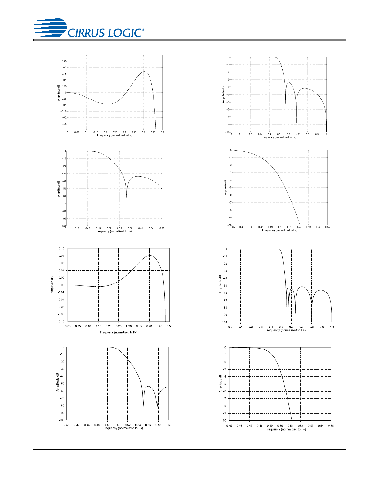
10.ADC AND DAC DIGITAL FILTERS
Figure 26. ADC Passband Ripple Figure 27. ADC Stopband Rejection
Figure 28. ADC Transition Band Figure 29. ADC Transition Band (Detail)
Figure 30. DAC Passband Ripple Figure 31. DAC Stopband
Figure 32. DAC Transition Band Figure 33. DAC Transition Band (Detail)
3/1/13
CS42L52
78 DS680F2
Page 79

11.PARAMETER DEFINITIONS
Dynamic Range
The ratio of the rms value of the signal to the rms sum of all other spectral components over the specified
bandwidth. Dynamic Range is a signal-to-noise ratio measurement over the specified band width made with
a -60 dBFS signal. 60 dB is added to resulting measurement to refer the measurement to full-scale. This
technique ensures that the distortion components ar e below the n oise level an d do n ot affect the m easu rement. This measurement technique has been accepted by the Audio Engineering Society, AES17-1991,
and the Electronic Industries Association of Japan, EIAJ CP-307. Expressed in decibels.
Total Harmonic Distortion + Noise
The ratio of the rms value of the signal to the rms sum of all other spectral components over the specified
band width (typically 10 Hz to 20 kHz), including distortion components. Expressed in decibels. Measured
at -1 and -20 dBFS as suggested in AES17-1991 Annex A.
Frequency Response
A measure of the amplitude response variation from 10 Hz to 20 kHz relative to the amplitude response at
1 k Hz. Units in decibels.
Interchannel Isolation
3/1/13
CS42L52
A measure of crosstalk between the left and right channel pairs. Mea sured for ea ch channel at the co nverter's output with no signal to the input under test and a full-scale signa l applied to the other channel. Units in
decibels.
Interchannel Gain Mismatch
The gain difference between left and right channel pairs. Units in decibels.
Gain Drift
The change in gain value with temperature. Units in ppm/°C.
Offset Error
The deviation of the mid-scale transition (111...111 to 000...000) from the ideal. Units in mV.
DS680F2 79
Page 80

12.PACKAGE DIMENSIONS
40L QFN (6 X 6 mm BODY) PACKAGE DRAWING
eb
A
A1
PIN #1
IDENTIFIER
0.500.10
LASER
MARKING
E
2.00 REF
D2
L
PIN #1 CORNER
2.00 REF
E2
D
3/1/13
CS42L52
INCHES MILLIMETERS NOTE
DIM MIN NOM MAX MIN NOM MAX
A----0.0394----1.001
A1 0.0000 -- 0.0020 0.00 -- 0.05 1
b 0.0071 0.0091 0.0110 0.18 0.23 0.28 1,2
D 0.2362 BSC 6.00 BSC 1
D2 0.1594 0.1614 0.1634 4.05 4.10 4.15 1
E 0.2362 BSC 6.00 BSC 1
E2 0.1594 0.1614 0.1634 4.05 4.10 4.15 1
e 0.0197 BSC 0.50 BSC 1
L 0.0118 0.0157 0.0197 0.30 0.40 0.50 1
JEDEC #: MO-220
Controlling Dimension is Millimeters.
1. Dimensioning and tolerance per ASME Y 14.5M-1995.
2. Dimensioning lead width applies to the plated terminal and is measu red between 0.20 mm and 0.25 mm
from the terminal tip.
THERMAL CHARACTERISTICS
Junction to Ambient Thermal Impedance 2 Layer Board
Parameter Symbol Min Typ Max Units
4 Layer Board
JA
-
-
44
19
-
°C/Watt
-
80 DS680F2
Page 81

3/1/13
CS42L52
13.ORDERING INFORMATION
Product Description Package Pb-Free Grade Temp Range Container Order #
CS42L52
CDB42L52
CRD42L52
Low-Power, Stereo
CODEC with Headphone
and Speaker Amps
CS42L52 Evaluation
Board
CS42L52 Reference
Design
40L-QFN Yes Commercial -40 to +85° C
- No - - - CDB42L52
- No - - - CRD42L52
Rail CS42L52-CNZ
Tape and Reel CS42L52-CNZR
14.REFERENCES
1. Philips Semiconductor, The I²C-Bus Specification: Version 2.1, January 2000.
http://www.semiconductors.philips.com
.
15.REVISION HISTORY
Revision Changes
F1 Initial draft
Removed the Automotive specification.
Added AD0 characteristics to “I/O Pin Characteristics” on page 10.
Added AD0 pin to Figure 1. Typical Connection Diagram on page 11.
Updated Note 6 on page 15.
specification for VL = 1.8 V in “Digital Interface Specifications and Characteristics” on page 22.
IH
F2
Updated the V
Updated “PWM Outputs” on page 32 to exclude support of a 384x MCLK to LR CK ratio.
Added register commands for entering and exiting DSP 16-bit, 8 kHz Fs, SCLK = MCLK, master mode in section
“DSP Mode” on page 35.
Updated Section 4.9 “Recommended Power-up Sequence” on page 37.
Updated Section 4.10 “Recommended Power-Down Sequence” on page 37.
Added a description of the AD0 pin to “I²C Control” on page 38.
Added AD0 detail to Figure 20. Control Port Timing, I²C Write on page 38 and Figure 21. Control Port Timing, I²C
Read on page 39.
Updated the first paragraph in “Register Quick Reference” on page 40 to allow for data sheet-specified controlwrites to reserved registers.
Removed I²C address heading row from “Register Quick Reference” on page 40.
Updated notes in “Auto-Detect” on page 44.
Updated table in “Speed Mode” on page 45.
Added note 1 in “Freeze Registers” on page 52.
Updated notes in “Digital Soft Ramp” on page 53.
Added note 4 to “Digital Zero Cross” on page 53.
Added notes 1 and 2 for ALC configuration in “ALC Enable and Attack Rate (Address 2Ah)” on page 67.
Corrected the E2 scale in the package drawing in “Package Dimensions” on page 80.
DS680F2 81
Page 82

3/1/13
Contacting Cirrus Logic Support
For all product questions and inquiries, contact a Cirrus Logic Sales Representative.
To find one nearest you, go to www.cirrus.com.
IMPORTANT NOTICE
Cirrus Logic, Inc. and its subsidiaries (“Cirrus”) believe that the information contained in this document is accurate and reliable. However, the information is subject
to change without noti ce and is provided “AS IS” wi thout war ranty of any kind (express or impli ed). Cust omers ar e advise d to ob tain the latest version of relevant
information to verify, before placing orders, that information being relied on is current and complete. All products are sold subject to the terms and conditions of sale
supplied at the time of order acknowled gment, includin g those pertaining to wa rranty, indemnificatio n, and limitation of liability. No responsibility is assumed by Cirrus
for the use of this information, including use of this information as the basis for manufacture or sale of any items, or for infringement of patents or other rights of third
parties. This document is the property of Cirrus and by furnishing this information, Cirrus grants no lice nse, express or implied under any patents, mask work rights,
copyrights, trademarks, trade secrets or other intellectual property rights. Cirrus owns the copyrights associated with the information contained herein and g ives consent for copies to be made of the information only for use within your organization with respect to Cirrus integrated circuits or other products of Cirrus. This consent
does not extend to other copying such as copying for general distribution, advertising or promotional purposes, or for creating any work for resale.
CERTAIN APPLICATIONS USING SEMICONDUCTOR PRODUCTS MAY INVOLVE POTENTIAL RISKS OF DEATH, PERSONAL INJURY, OR SEVERE PROPERTY OR ENVIRONMENTAL DAMAGE (“CRITICAL APPLICATIONS”). CIRRUS PRODUCTS ARE NOT DESIGNED, AUTHORIZED OR WARRANTED FOR USE
IN PRODUCTS SURGICALLY IMPLANTED INTO THE BODY, AUTOMOTIVE SAFETY OR SECURITY DEVICES, LIFE SUPPORT PRODUCTS OR OTHER CRITICAL APPLICATIONS. INCLUSION OF CIRRUS PRODUCTS IN SUCH APPLICATIONS IS UNDERSTOOD TO BE FULLY AT THE CUSTOMER’S RISK AND CIRRUS DISCLAIMS AND MAKES NO WARRANTY, EXPRESS, STATUTORY OR IMPLIED, INCLUDING THE IMPLIED WARRANTIES OF MERCHANTABILITY AND
FITNESS FOR PARTICULAR PURPOSE, WITH REGARD TO ANY CIRRUS PRODUCT THAT IS USED IN SUCH A MANNER. IF THE CUSTOMER OR CUSTOMER’S CUSTOMER USES OR PERMITS THE USE OF CIRRUS PRODUCTS IN CRITICAL APPLICATIONS, CUSTOMER AGREES, BY SUCH USE, TO FULLY
INDEMNIFY CIRRUS, ITS OFFICERS, DI RECTORS, EMPL OYEES, DIST RIBUT ORS AND OTHER AGENTS FROM ANY AND ALL LIABILITY, INCLUDING ATTORNEYS’ FEES AND COSTS, THAT MAY RESULT FROM OR ARISE IN CONNECTION WITH THESE US ES .
Cirrus Logic, Cirrus, and the Cirrus Logic logo designs are trademarks of Cirrus Logic, Inc. All other brand and product names in this document may be trademarks
or service marks of their respective owners.
I²C is a trademark of Philips Semiconductor.
CS42L52
82 DS680F2
 Loading...