

Page 1
CS4272
24-Bit, 192 kHz Stereo Audio CODEC
D/A Features
! High Performance
– 114 dB Dynamic Range
– -100 dB THD+N
! Up to 192 kHz Sampling Rates
! Differential Analog Architecture
! Volume Control with Soft Ramp
– 1 dB Step Size
– Zero Crossing Click-free Transitions
! Selectable Digital Filters
– Fast and Slow Roll Off
! ATAPI Mixing Functions
! Selectable Serial Audio Interface Formats
– Left Justified up to 24-bit
2
–I
S up to 24-bit
– Right Justified 16-, 18-, 20-, and 24-Bit
! Control Output for External Muting
! Selectable 50/15 µs De-emphasis
A/D Features
! High Performance
– 114 dB Dynamic Range
– -100 dB THD+N
! Up to 192 kHz Sampling Rates
! Differential Analog Architecture
! Multi-bit Delta Sigma Conversion
! High-pass Filter or DC Offset Calibration
! Low-Latency Digital Anti-alias Filtering
! Automatic Dithering of 16-bit Data
! Selectable Serial Audio Interface Formats
– Left Justified up to 24-bit
2
–I
S up to 24-bit
System Features
! Direct Interface with 5V to 2.5V Logic Levels
! Internal Digital Loopback
! On-chip Oscillator
! Stand-Alone or Control Port Functionality
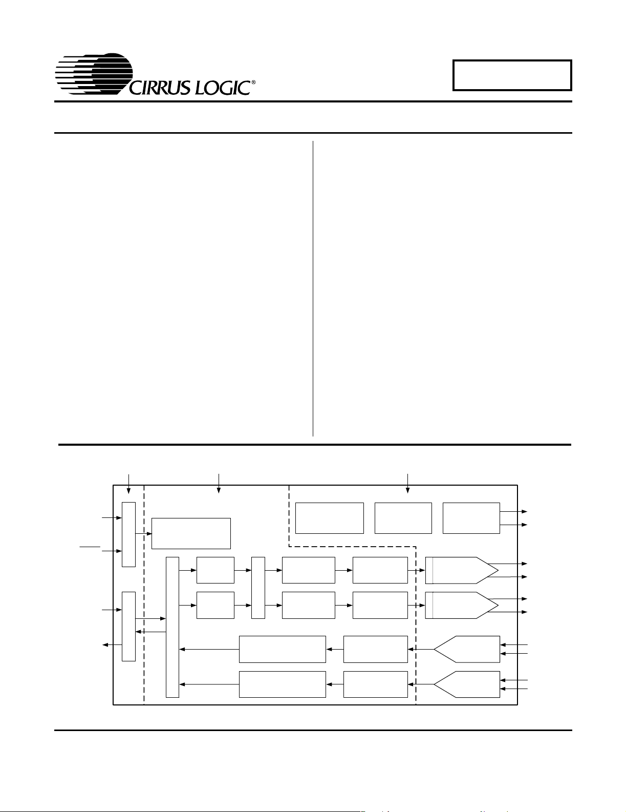
2.5 V to 5 V
Hardware or
2
I
C/SPI
Control Data
Reset
Serial
Audio
Input
Serial
Audio
Output
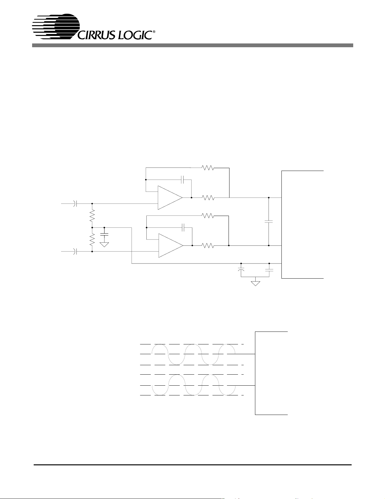
Cirrus Logic, Inc.
www.cirrus.com
Register / Hardware
Configuration
Level TranslatorLevel Translato r
3.3 V to 5 V 5 V
Internal Voltage
Reference
Volume
Control
Volume
Control
High Pass Filter &
DC Offset Calibration
PCM Serial Interface / Loopback
High Pass Filter &
DC Offset Calibration
Copyright © Cirrus Logic, Inc. 2005
Selectable
Interpolation
Filter
Mixer
Selectable
Interpolation
Filter
(All Rights Reserved)
∆Σ Modulator
∆Σ Modulator
Low-Latency
Anti-Alias Filter
Low-Latency
Anti-Alias Filter
Internal
Oscillator
External
Mute Control
Switched Capacitor
DAC and Filter
Switched Capacitor
DAC and Filter
Multibit
Oversampling
ADC
Multibit
Oversampling
ADC
Left and
Right Mute
Controls
Left
Differential
Output
Right
Differential
Output
Left
Differential
Input
Right
Differential
Input
AUGUST '05
DS593F1
Page 2
CS4272
Stand-Alone Mode Feature Set
! System Features
– Serial Audio Port Master or Slave Operation
– Internal Oscillator for Master Clock
!
D/A Features
– Auto-mute on Static Samples
– 44.1 kHz 50/15 µs De-emphasis Available
– Selectable Serial Audio Interface Formats
"Left Justified up to 24-bit
2
"I
S up to 24-bit
A/D Features
!
– Automatic Dithering for 16-bit Data
– High-pass Filter
– Selectable Serial Audio Interface Formats
"Left Justified up to 24-bit
2
"I
S up to 24-bit
Software Mode Feature Set
! System Features
– Serial Audio Port Master or Slave Operation
– Internal Oscillator for Master Clock
– Internal Digital Loopback Available
!
D/A Features
– Selectable Auto-mute
– Selectable Interpolation Filters
– Selectable 32-, 44.1-, and 48-kHz De-emphasis
Filters
– Configurable ATAPI Mixing Functions
– Configurable Volume and Muting Controls
– Selectable Serial Audio Interface Formats
"Left Justified up to 24-bit
2
"I
S up to 24-bit
"Right Justified 16, 18, 20, and 24-bit
!
A/D Features
– Selectable Dithering for 16-bit Data
– Selectable High-pass Filter or DC Offset Calibration
– Selectable Serial Audio Interface Formats
"Left Justified up to 24-bit
2
"I
S up to 24-bit
General Description
The CS4272 is a high-performance, integrated audio
CODEC. The CS4272 performs stereo analog-to-digita l
(A/D) and digital-to-analog (D/A) conversion of up to
24-bit serial values at sample rates up to 192 kHz.
The D/A offers a volume control that operates with a
1 dB step size. It incorporates selectable soft ramp and
zero crossing transition functions to eliminate clicks and
pops.
The D/A’s integrated digital mixing functions allow a variety of output configurations ranging from a channel
swap to a stereo-to-mono downmix.
Standard 50/15 µs de-emphasis is available for sampling rates of 32, 44.1, and 48 kHz for compatibility with
digital audio programs mastered using the 50/15 µs preemphasis technique.
Integrated level translators allow easy interfacing between the CS4272 and other devices operating over a
wide range of logic levels.
An on-chip oscillator eliminates the need for an external
crystal oscillator circuit. This can reduce overall design
cost and conserve circuit board space. The CS4272 automatically uses the on-chip oscillator in the absence of
an applied master clock, making this feature easy to
use.
Independently addressable high-pass filters are available for the right and left channel of the A/D. This allows
the A/D to be used in a wide variety of applications
where one audio channel and one DC measurement
channel is desired.
The CS4272’s wide dynamic range, negligible distortion, and low noise make it ideal for applications such as
A/V receivers, DVD-R, CD-R, digital mixing consoles,
effects processors, set-top box systems, and automotive audio systems.
Ordering Information
Product Description Package Pb-Free Grade Temp Range Container Order #
CS4272
CDB4272 CS4272 Evaluation Board No - - - CDB4272
24-Bit, 192 kHz
Stereo Audio CODEC
28-pin
TSSOP
YES
Commercial -10° to +70° C
Automotive -40° to +85° C
2 DS593F1
Tube CS4272-CZZ
Tape & Reel CS4272-CZZR
Tube CS4272-DZZ
Tape & Reel CS4272-DZZR
Page 3

TABLE OF CONTENTS
1. PIN DESCRIPTIONS - SOFTWARE MODE ............................................................................. 5
2. PIN DESCRIPTIONS - STAND-ALONE MODE ....................................................................... 7
3. CHARACTERISTICS AND SPECIFICATIONS ........................................................................ 9
SPECIFIED OPERATING CONDITIONS................................................................................. 9
ABSOLUTE MAXIMUM RATINGS........................................................................................... 9
DAC ANALOG CHARACTERISTICS - COMMERCIAL GRADE............................................ 10
DAC ANALOG CHARACTERISTICS - AUTOMOTIVE GRADE ............................................ 11
DAC COMBINED INTERPOLATION & ON-CHIP ANALOG FILTER RESPONSE................ 12
ADC ANALOG CHARACTERISTICS - COMMERCIAL GRADE............................................ 14
ADC ANALOG CHARACTERISTICS - AUTOMOTIVE GRADE ............................................ 15
ADC DIGITAL FILTER CHARACTERISTICS......................................................................... 16
DC ELECTRICAL CHARACTERISTICS ............................................................. .... ............... 17
DIGITAL CHARACTERISTICS............................................................................................... 17
SWITCHING CHARACTERISTICS - SERIAL AUDIO PORT................................................. 18
SWITCHING CHARACTERISTICS - I²C MODE CONTROL PORT....................................... 21
SWITCHING CHARACTERISTICS - SPI CONTROL PORT ................................................. 22
4. TYPICAL CONNECTION DIAGRAM ..................................................................................... 23
5. APPLICATIONS ..................................................................................................................... 24
5.1 Stand-Alone Mode .............. ... .... ... ... ... ... ....................................... ... .... ... .........................24
5.1.1 Recommended Power-Up Sequence ................................................................. 24
5.1.2 Master/Slave Mode ....... ... ... ... ... .... ... ................................................................... 24
5.1.3 System Clocking .............. ... ....................................... ... ...................................... 24
5.1.3.1 Crystal Applications (XTI/XTO) ........................................................... 24
5.1.3.2 Clock Ratio Selection .......................................................................... 25
5.1.4 16-Bit Auto-Dither ............................................................................................... 26
5.1.5 Auto-Mute ............................................................... ... ... ... ................................... 26
5.1.6 High Pass Filter ................................................................................................... 26
5.1.7 Interpolation Filter .............................................................................................. 26
5.1.8 Mode Selection & De-Emphasis ............................. ... ... ...................................... 26
5.1.9 Serial Audio Interface Format Selection ............................................................. 26
5.2 Control Port Mode .................................................. ... ... ... .... ... ... ... ... .... ............................ 27
5.2.1 Recommended Power-Up Sequence - Access to Control Port Mode ................ 27
5.2.2 Master / Slave Mode Selection ..................... ... ... .... ... ... ...................................... 27
5.2.3 System Clocking .............. ... ....................................... ... ...................................... 27
5.2.3.1 Crystal Applications (XTI/XTO) ........................................................... 27
5.2.3.2 Clock Ratio Selection .......................................................................... 28
5.2.4 Internal Digital Loopback ........................................................... ... ... .... ... ... ... ... ... 30
5.2.5 Dither for 16-Bit Data .......................................................................................... 30
5.2.6 Auto-Mute ............................................................... ... ... ... ................................... 30
5.2.7 High Pass Filter and DC Offset Calibration ......................................................... 30
5.2.8 Interpolation Filter .............................................................................................. 31
5.2.9 De-Emphasis ................................................................ ... ... .... ... ... ...................... 31
5.2.10 Oversampling Modes ........................................................................................ 31
5.3 De-Emphasis Filter .......................................................................................................... 31
5.4 Analog Connections ............................................... ... ... ... .... ... ... ... ................................... 32
5.4.1 Input Connections .. ... ....................................... ... .... ... ...................................... ... 32
5.4.2 Output Connections ......................... ... ... .... ... ....................................... ... ... ... ... ... 33
5.5 Mute Control ....................................... ... .... ...................................... .... ... ... ...................... 34
5.6 Synchronization of Multiple Devices ................................................................................ 34
5.7 Grounding and Power Supply Decoupling ....................................................................... 34
6. CONTROL PORT INTERFACE .............................................................................................. 35
CS4272
DS593F1 3
Page 4

CS4272
6.1 SPI Mode ............................... .... ... ....................................... ... ... ...................................... 35
6.2 I²C Mode .................................................................... ... ... .... ............................................ 36
7. REGISTER QUICK REFERENCE .......................................................................................... 37
8. REGISTER DESCRIPTION .................................................................................................... 38
8.1 Mode Control 1 - Address 01h ............... .... ... ... ... .... ...................................... .... ... ... ... ... ... 38
8.1.1 Functional Mode (Bits 7:6) ..................................................................................38
8.1.2 Ratio Select (Bits 5:4) ...................................................... ... ................................ 38
8.1.3 Master / Slave Mode (Bit 3) .................... .... ... ... ....................................... ... ... ... ... 38
8.1.4 DAC Digital Interface Format (Bits 2:0) ......................... ...................................... 38
8.2 DAC Control - Address 02h ... ....................................... ... .... ... ... ... ... .... ... ... ... ...................39
8.2.1 Auto-Mute (Bit 7) ..................................................................................... ... ... ... ... 39
8.2.2 Interpolation Filter Select (Bit 6) .......................................................................... 39
8.2.3 De-Emphasis Control (Bits 5:4) .................. ... ... ... .... ... ... ... ................................... 39
8.2.4 Soft Volume Ramp-Up After Error (Bit 3) ............................................................ 40
8.2.5 Soft Ramp-Down Before Filter Mode Change (Bit 2) ..........................................40
8.2.6 Invert Signal Polarity (Bits 1:0) ............................ .... ... ... ... ... .... ... ... ... ...................40
8.3 DAC Volume & Mixing Control - Address 03h .... .... ... ... ... .... ... ... ... ... .... ... ... ... .... ... ... .........40
8.3.1 Channel B Volume = Channel A Volume (Bit 6) ..................... ... ... ... .... ... ... .........40
8.3.2 Soft Ramp or Zero Cross Enable (Bits 5:4) ......................................................... 40
8.3.3 ATAPI Channel Mixing and Muting (Bits 3:0) ......................................................41
8.4 DAC Channel A Volume Control - Address 04h ..............................................................42
8.5 DAC Channel B Volume Control - Address 05h ..............................................................42
8.5.1 Mute (Bit 7) ..........................................................................................................42
8.5.2 Volume Control (Bits 6:0) ................................................. ................................... 42
8.6 ADC Control - Address 06h ... ....................................... ... .... ... ... ... ... .... ... ... ... ...................43
8.6.1 Dither for 16-Bit Data (Bit 5) ................................................................................ 43
8.6.2 ADC Digital Interface Format (Bit 4) ....................................................................43
8.6.3 ADC Channel A & B Mute (Bits 3:2) ........................... ... ... ... .... ... ... ... .... ... ... ... ... ... 43
8.6.4 Channel A & B High Pass Filter Disable (Bits 1:0) ..... ...................................... ... 43
8.7 Mode Control 2 - Address 07h ............... .... ... ... ... .... ... ... ... ....................................... ... ... ... 43
8.7.1 Digital Loopback (Bit 4) ........................................... ... ... ... ... .... ............................ 43
8.7.2 AMUTEC = BMUTEC (Bit 3) ............................................................................... 43
8.7.3 Freeze (Bit 2) ............................................................. ... ... ... .... ............................ 44
8.7.4 Control Port Enable (Bit 1) ............... ................................................................... 44
8.7.5 Power Down (Bit 0) .............................................................................................44
8.8 Chip ID - Register 08h .....................................................................................................44
8.8.1 Chip ID (Bits 7:4) .................................................................................................44
8.8.2 Chip Revision (Bits 3:0) .......................................................................................44
9. PARAMETER DEFINITIONS .................................................................................................. 45
10. PACKAGE DIMENSIONS ..................................................................................................... 46
11. APPENDIX ............................................... ... .... ... ... ... ....................................... ... .... ... ............47
4 DS593F1
Page 5
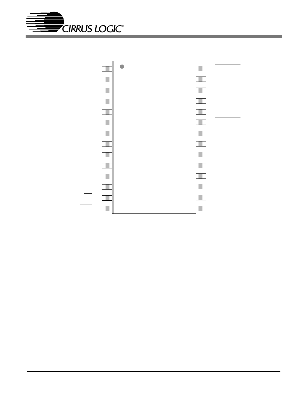
1. PIN DESCRIPTIONS - SOFTWARE MODE
CS4272
XTO BMUTEC
XTI AOUTB-
MCLK AOUTB+
LRCK AOUTA+
SCLK AOUTA-
SDOUT AMUTEC
SDIN FILT+
DGND AGND
VD VA
VL AINB-
SCL/CCLK AINB+
SDA/CDIN AINA+
AD0/CS AINA-
RST VCOM
1
2
3
4
5
6
7
821
9
10
11
12 17
13
14 15
28-Pin TSSOP
28
27
26
25
24
23
22
20
19
18
16
DS593F1 5
Page 6
Pin Name # Pin Description
XTO
XTI
MCLK
LRCK
SCLK
SDOUT
SDIN
DGND
VD
VL
SCL/CCLK
SDA/CDIN
AD0/CS
Crystal Connections (Input/Output) - I/O pins for an external crystal which may be used to generate
1,2
MCLK. See “Crystal Applications (XTI/XTO)” on page 24 or “Crystal Applications (XTI/XTO)” on page 27.
Master Clock (Input/Output) -Clock source for the delta-sigma modulators. See “Crystal Applications
3
(XTI/XTO)” on page 24 or “Crystal Applications (XTI/XTO)” on page 27.
Left Right Clock (Input/Output) - Determines which channel, Left or Right, is currently active on the
4
serial audio data line.
Serial Clock (Input/Output) - Serial clock for the serial audio interface.
5
Serial Audio Data Output (Output) - Output for two’s complement serial audio data.
6
Serial Audio Data Input (Input) - Input for two’s complement serial audio data.
7
Digital Ground (Input) - Ground reference for the internal digital section.
8
Digital Power (Input) - Positive power for the internal digital section.
9
Logic Power (Input) - Positive power for the digital input/output interface.
10
Serial Control Port Clock (Input) - Serial clock for the serial control port.
11
Serial Control Data (Input/Output) - SDA is a data I/O in I²C mode. CDIN is the input data line for the
12
control port interface in SPI mode.
Address Bit 0 (I²C) / Control Port Chip Select (SPI) (Input) - AD0 is a chip address pin in I²C mode; CS
13
is the chip select signal for SPI format.
CS4272
RST
VCOM
AINAAINA+
AINB+
AINB-
VA
AGND
FILT+
AMUTEC
AOUTAAOUTA+
AOUTB+
AOUTB-
BMUTEC
Reset (Input) - The device enters a low power mode when this pin is driven low.
14
Common Mode Voltage (Output) - Filter connection for internal common mode voltage.
15
16,
17,
Differential Analog Input (Input) - The full scale differential input signals are presented to the deltasigma modulators. The full scale level is specified in the ADC Analog Characteristics specification table.
18,
19
Analog Power (Input) - Positive power for the internal analog section.
20
Analog Ground (Input) - Ground reference for the internal analog section.
21
Positive Voltage Reference (Output) - Positive reference voltage for the internal sampling circuits.
22
Channel A Mute Control (Output) - This pin is active during power-up initialization, reset, muting, when
23
master clock to left/right clock frequency ratio is incorrect, or power-down.
24,
25,
Differential Analog Audio Output (Output) - The full scale differential output level is specified in the
DAC Analog Characteristics specification table.
26,
27
Channel B Mute Control (Output) - This pin is active during power-up initialization, reset, muting, when
28
master clock to left/right clock frequency ratio is incorrect, or power-down.
6 DS593F1
Page 7

2. PIN DESCRIPTIONS - STAND-ALONE MODE
CS4272
XTO BMUTEC
XTI AOUTB-
MCLK AOUTB+
LRCK AOUTA+
SCLK AOUTA-
SDOUT (M/S)AMUTEC
SDIN FILT+
DGND AGND
VD VA
VL AINBM0 AINB+
M1 AINA+
I2S/LJ AINA-
RST VCOM
1
2
3
4
5
6
7
821
9
10
11
12 17
13
14 15
28-Pin TSSOP
28
27
26
25
24
23
22
20
19
18
16
DS593F1 7
Page 8

Pin Name # Pin Description
XTO
XTI
MCLK
LRCK
SCLK
SDOUT
(M/S
)
SDIN
DGND
VD
VL
M0
M1
Crystal Connections (Input/Output) - I/O pins for an external crystal which may be used to generate the
master clock. See “Crystal Applications (XTI/XTO)” on page 24 or “Crystal Applications (XTI/XTO)” on
1,2
page 27.
Master Clock (Input/Output) -Clock source for the delta-sigma modulators. See “Crystal Applications
3
(XTI/XTO)” on page 24 or “Crystal Applications (XTI/XTO)” on page 27.
Left Right Clock (Input/Output) - Determines which channel, Left or Right, is currently active on the
4
serial audio data line.
Serial Clock (Input/Output) - Serial clock for the serial audio interface.
5
Serial Audio Data Output (Output) - Output for two’s complement serial audio data. This pin must be
6
pulled-up or pulled-down to select Master or Slave Mode. See “Master/Slave Mode” on page 24.
Serial Audio Data Input (Input) - Input for two’s complement serial audio data.
7
Digital Ground (Input) - Ground reference for the internal digital section.
8
Digital Power (Input) - Positive power for the internal digital section.
9
Logic Power (Input) - Positive power for the digital input/output interface.
10
Mode Select 0 (Input) - In conjunction with M1, selects operating mode. Functionality is described in the
11
Hardware Mode Speed Configuration table.
Mode Select 1 (Input) - In conjunction with M0, selects operating mode. Functionality is described in the
12
Hardware Mode Speed Configuration table.
CS4272
I2S/LJ
RST
VCOM
AINAAINA+
AINB+
AINB-
VA
AGND
FILT+
AMUTEC
AOUTAAOUTA+
AOUTB+
AOUTB-
BMUTEC
Serial Audio Interface Select (Input) - Selects either the left-justified or I2S format for the Serial Audio
13
Interface.
Reset (Input) - The device enters a low power mode when this pin is driven low.
14
Common Mode Voltage (Output) - Filter connection for internal common mode voltage.
15
16,
17,
Differential Analog Input (Input) - The full scale differential input signals are presented to the deltasigma modulators. The full scale level is specified in the ADC Analog Characteristics specification table.
18,
19
Analog Power (Input) - Positive power for the internal analog section.
20
Analog Ground (Input) - Ground reference for the internal analog section.
21
Positive Voltage Reference (Output) - Positive reference voltage for the internal sampling circuits.
22
Channel A Mute Control (Output) - This pin is active during power-up initialization, reset, muting, when
23
master clock to left/right clock frequency ratio is incorrect, or power-down.
24,
25,
Differential Analog Audio Output (Output) - The full scale differential output level is specified in the
Analog Characteristics specification table.
26,
27
Channel B Mute Control (Output) - This pin is active during power-up initialization, reset, muting, when
28
master clock to left/right clock frequency ratio is incorrect, or power-down.
8 DS593F1
Page 9
CS4272
3. CHARACTERISTICS AND SPECIFICATIONS
(All Min/Max characteristics and specifications are guaranteed over the Specified Operating Conditions. Typical
performance characteristics and specifications are derived from measurements taken at nominal supply voltages
and T
SPECIFIED OPERATING CONDITIONS (AGND = 0 V; all voltages with respect to ground.)
ABSOLUTE MAXIMUM RATINGS (GND = 0 V, All voltages with respect to ground.) (Note 1)
= 25°C.)
A
Parameters Symbol Min Nom Max Units
DC Power Supplies: Positive Analog
Positive Digital
Positive Logic
Ambient Operating Temperature (Power Applied)
Commercial Grade
Automotive Grade
Parameter Symbol Min Typ Max Units
DC Power Supplies: Analog
Logic
Digital
Input Current (Note 2) I
Analog Input Voltage V
Digital Input Voltage V
Ambient Operating Temperature (Power Applied) T
Storage Temperature T
VA
VD
VL
T
A
VA
VL
VD
in
IND
stg
4.75
3.1
2.37
-10
-40
-0.3
-0.3
-0.3
IN
A
GND-0.3 - VA+0.3 V
-0.3 - VL+0.3 V
-50 - +95 °C
-65 - +150 °C
5.0
3.3
3.3
-
-
--±10 mA
5.25
5.25
5.25
+70
+85
-
-
-
+6.0
+6.0
+6.0
V
V
V
°C
°C
V
V
V
Notes: 1. Operation beyond these limits may result in permanent damage to the device.
Normal operation is not guaranteed at these extremes.
2. Any pin except supplies. Transient currents of up to ±100 mA on the analog input pins will not cause
SCR latch-up.
DS593F1 9
Page 10

CS4272
DAC ANALOG CHARACTERISTICS - COMMERCIAL GRADE (Notes 3 to 7)
Parameter Symbol Min Typ Max Unit
Dynamic Performance
Dynamic Range 24-Bit s A-Weighted
unweighted
16-Bits unweighted
Total Harmonic Distortion + Noise 0 dB
THD+N -
-20 dB
-60 dB
Idle Channel Noise / Signal-to-Noise Ratio - 114 - dB
Interchannel Isolation (1 kHz) - 100 - dB
DC Accuracy
Interchannel Gain Mismatch ICGM - 0.1 - dB
Gain Drift - 100 - ppm/°C
Analog Output Characteristics and Specifications
Full Scale Differential Output Voltage V
Output Resistance (note 7) Z
Minimum AC-Load Resistance R
Maximum Load Capacitance C
0.91xVA 0.96xVA 1.01xVA Vpp
FS
out
L
L
108
105
-
-
-
114
111
94
-100
-91
-51
-
-
-
-94
-
-45
- 100 - Ω
-3-kΩ
- 100 - pF
dB
dB
dB
dB
dB
dB
Notes: 3. One-half LSB of Triangular PDF dither is added to data.
4. Performance measur ements ta ken with a full-scale 997 Hz sine wave under Test load R
10 pF
5. Measurement bandwidth is 10 Hz to 20 kHz.
6. Logic “0” = GND = 0V; Logic “1” = VL; VL = VA unless otherwise noted.
7. V
is tested under load RL but does not include attenuation due to Z
FS
OUT
= 3 kΩ, CL =
L
10 DS593F1
Page 11

CS4272
DAC ANALOG CHARACTERISTICS - AUTOMOTIVE GRADE (Notes 3 to 7)
Parameter Symbol Min Typ Max Unit
Dynamic Performance
Dynamic Range 24-Bit s A-Weighted
unweighted
16-Bits unweighted
Total Harmonic Distortion + Noise 0 dB
-20 dB
-60 dB
Idle Channel Noise / Signal-to-Noise Ratio - 114 - dB
Interchannel Isolation (1 kHz) - 100 - dB
DC Accuracy
Interchannel Gain Mismatch ICGM - 0.1 - dB
Gain Drift - 100 - ppm/°C
Analog Output Characteristics and Specifications
Full Scale Differential Output Voltage V
Output Resistance (note 7) Z
Minimum AC-Load Resistance R
Maximum Load Capacitance C
THD+N -
0.91xVA 0.96xVA 1.01xVA Vpp
FS
out
L
L
106
103
-
-
-
- 100 - Ω
-3-kΩ
- 100 - pF
114
111
94
-100
-91
-51
-
-
-
-92
-
-43
dB
dB
dB
dB
dB
dB
DS593F1 11
Page 12
CS4272
DAC COMBINED INTERPOLATION & ON-CHIP ANALOG FILTER RESPONSE
(Note 12)
Fast Roll-Off
Parameter
Single Speed Mode - 48 kHz
Passband (Note 9) to -0.01 dB corner
to -3 dB corner
Frequency Response 10 Hz to 20 kHz -0.01 - +0.01 dB
StopBand .547 - - Fs
StopBand Attenuation (Note 10) 90 - - dB
Group Delay - 12/Fs - s
De-emphasis Error (Note 11) Fs = 32 kHz
(Relative to 1kHz) Fs = 44.1 kHz
Fs = 48 kHz
Double Speed Mode - 96 kHz
Passband (Note 9) to -0.01 dB corner
to -3 dB corner
Frequency Response 10 Hz to 20 kHz -0.01 - 0.01 dB
StopBand .583 - - Fs
StopBand Attenuation (Note 10) 80 - - dB
Group Delay - 4.6/Fs - s
Quad Speed Mode - 192 kHz
Passband (Note 9) to -0.01 dB corner
to -3 dB corner
Frequency Response 10 Hz to 20 kHz -0.01 - 0.01 dB
StopBand .635 - - Fs
StopBand Attenuation (Note 10) 90 - - dB
Group Delay - 4.7/Fs - s
0
0
-
-
-
0
0
0
0
-
-
-
-
-
-
-
-
-
.454
.499
±0.23
±0.14
±0.09
.430
.499
.105
.490
UnitMin Typ Max
Fs
Fs
dB
dB
dB
Fs
Fs
Fs
Fs
12 DS593F1
Page 13

CS4272
DAC COMBINED INTERPOLATION & ON-CHIP ANALOG FILTER RESPONSE
(cont) (Note 12)
Slow Roll-Off (Note 8)
Parameter
Single Speed Mode - 48 kHz
Passband (Note 9) to -0.01 dB corner
to -3 dB corner
Frequency Response 10 Hz to 20 kHz -0.01 - +0.01 dB
StopBand .583 - - Fs
StopBand Attenuation (Note 10) 64 - - dB
Group Delay - 6.5/Fs - s
De-emphasis Error (Note 11) Fs = 32 kHz
(Relative to 1 kHz) Fs = 44.1 kHz
Fs = 48 kHz
Double Speed Mode - 96 kHz
Passband (Note 9) to -0.01 dB corner
to -3 dB corner
Frequency Response 10 Hz to 20 kHz -0.01 - 0.01 dB
StopBand .792 - - Fs
StopBand Attenuation (Note 10) 70 - - dB
Group Delay - 3.9/Fs - s
Quad Speed Mode - 192 kHz
Passband (Note 9) to -0.01 dB corner
to -3 dB corner
Frequency Response 10 Hz to 20 kHz -0.01 - 0.01 dB
StopBand .868 - - Fs
StopBand Attenuation (Note 10) 75 - - dB
Group Delay - 4.2/Fs - s
Notes: 8. Slow Roll-Off interpolation filter is only available in control port mode.
9. Response is clock dependent and will scale with Fs. Note that the response plots (Figures21 to 44) have
been normalized to Fs and can be de-normalized by multiplying the X-axis scale by Fs.
10. Single and Double Speed Mode Measurement Bandwidth is from stopband to 3 Fs.
Quad Speed Mode Measurement Bandwidth is from stopband to 1.34 Fs.
11. De-emphasis is available only in Single Speed Mode; Only 44.1 kHz De-emphasis is available in StandAlone Mode.
12. Plots of this data are contained in the “Appendix” on pag e 47. See Figure 21 through Figure 44.
0
0
-
-
-
0
0
0
0
-
-
-
-
-
-
-
-
-
0.417
0.499
±0.23
±0.14
±0.09
.296
.499
.104
.481
UnitMin Typ Max
Fs
Fs
dB
dB
dB
Fs
Fs
Fs
Fs
DS593F1 13
Page 14
CS4272
ADC ANALOG CHARACTERISTICS - COMMERCIAL GRADE
Measurement Bandwidth is 10 Hz to 20 kHz unless otherwise specified. Input is 1 kHz sine wave.
Parameter Symbol Min Typ Max Unit
Single Speed Mode Fs = 48 kHz
Dynamic Range A-weighted
unweighted
Total Harmonic Distortio n + Noise (Note 13)
-1 dB
-20 dB
-60 dB
Double Speed Mode Fs = 96 kHz
Dynamic Range A-weighted
unweighted
40 kHz bandwidth unweighted
Total Harmonic Distortio n + Noise (Note 13)
-1 dB
-20 dB
-60 dB
40 kHz bandwidth -1 dB
Quad Speed Mode Fs = 192 kHz
Dynamic Range A-weighted
unweighted
40 kHz bandwidth unweighted
Total Harmonic Distortio n + Noise (Note 13)
-1 dB
-20 dB
-60 dB
40 kHz bandwidth -1 dB
Dynamic Performance for All Modes
Interchannel Isolation - 110 - dB
Interchannel Phase Deviation - 0.0001 - Degree
DC Accuracy
Interchannel Gain Mismatch - 0.1 - dB
Gain Error Gain Drift Offset Error HPF enabled
HPF disabled
Analog Input Characteristics
Full-scale Input Voltage 1.07xVA 1.13xVA 1.19xVA Vpp
Input Impedance (Differential) (Note 14) 37 - - k
Common Mode Rejection Ratio CMRR - 82 - dB
THD+N
THD+N
THD+N
108
105
-
-
-
108
105
-
-
-
-
-
108
105
-
-
-
-
-
-
-
114
111
-100
-91
-51
114
111
108
-100
-91
-51
-97
114
111
108
-100
-91
-51
-97
-
-
-94
-
-
-
-
-
-94
-
-
-
-
-
-
-94
-
-
-
dB
dB
dB
dB
dB
dB
dB
dB
dB
dB
dB
dB
dB
dB
dB
dB
dB
dB
dB
±5%
±100 - ppm/°C
0
100
-
-
LSB
LSB
Ω
Notes: 13. Referred to the typical full-scale input voltage.
Notes: 14. Measured between AIN+ and AIN-
14 DS593F1
Page 15
CS4272
ADC ANALOG CHARACTERISTICS - AUTOMOTIVE GRADE
Measurement Bandwidth is 10 Hz to 20 kHz unless otherwise specified. Input is 1 kHz sine wave.)
Parameter Symbol Min Typ Max Unit
Single Speed Mode Fs = 48 kHz
Dynamic Range A-weighted
unweighted
Total Harmonic Distortio n + Noise (Note 15)
-1 dB
-20 dB
-60 dB
Double Speed Mode Fs = 96 kHz
Dynamic Range A-weighted
unweighted
40 kHz bandwidth unweighted
Total Harmonic Distortio n + Noise (Note 15)
-1 dB
-20 dB
-60 dB
40 kHz bandwidth -1 dB
Quad Speed Mode Fs = 192 kHz
Dynamic Range A-weighted
unweighted
40 kHz bandwidth unweighted
Total Harmonic Distortio n + Noise (Note 15)
-1 dB
-20 dB
-60 dB
40 kHz bandwidth -1 dB
Dynamic Performance for All Modes
Interchannel Isolation - 110 - dB
Interchannel Phase Deviation - 0.0001 - Degree
DC Accuracy
Interchannel Gain Mismatch - 0.1 - dB
Gain Error Gain Drift Offset Error HPF enabled
HPF disabled
Analog Input Characteristics
Full-scale Input Voltage 1.07xVA 1.13xVA 1.19xVA Vpp
Input Impedance (Differential) (Note 16) 37 - - k
Common Mode Rejection Ratio CMRR - 82 - dB
THD+N
THD+N
THD+N
106
103
-
-
-
106
103
-
-
-
-
-
106
103
-
-
-
-
-
-
-
114
111
-100
-91
-51
114
111
108
-100
-91
-51
-97
114
111
108
-100
-91
-51
-97
-
-
-92
-
-
-
-
-
-92
-
-
-
-
-
-
-92
-
-
-
dB
dB
dB
dB
dB
dB
dB
dB
dB
dB
dB
dB
dB
dB
dB
dB
dB
dB
dB
±5%
±100 - ppm/°C
0
100
-
-
LSB
LSB
Ω
Notes: 15. Referred to the typical full-scale input voltage.
Notes: 16. Measured between AIN+ and AIN-
DS593F1 15
Page 16
CS4272
ADC DIGITAL FILTER CHARACTERISTICS (Note 19)
Parameter Symbol Min Typ Max Unit
Single Speed Mode
Passband (-0.1 dB). (Note 17) 0 - 0.47 Fs
Passband Ripple. - - ±0.035 dB
Stopband. (Note 17) 0.58 - - Fs
Stopband Attenuation. -95 - - dB
Group Delay. t
Double Speed Mode
Passband (-0.1 dB). (Note 17) 0 - 0.45 Fs
Passband Ripple. - - ±0.035 dB
Stopband. (Note 17) 0.68 - - Fs
Stopband Attenuation. -92 - - dB
Group Delay. t
Quad Speed Mode
Passband (-0.1 dB). (Note 17) 0 - 0.24 Fs
Passband Ripple. - - ±0.035 dB
Stopband. (Note 17) 0.78 - - Fs
Stopband Attenuation. -97 - - dB
Group Delay. t
High Pass Filter Characteristics
Frequency Response -3.0 dB.
-0.13 dB. (Note 18)
Phase Deviation @ 20 Hz. (Note 18) - 10 - Deg
Passband Ripple. - - 0 dB
Filter Settling Time.
gd
gd
gd
-12/Fs- s
-9/Fs- s
-5/Fs- s
-120-
5
10
/Fs
-
Hz
Hz
s
Notes: 17. The filter frequency respon se scales precisely with Fs.
18. Response shown is for Fs equal to 48 kHz. Filter characteristics scale with Fs.
19. Plots of this data are contained in the “Appendix” on page 47. See Figure 45 through Figure 56.
16 DS593F1
Page 17

CS4272
DC ELECTRICAL CHARACTERISTICS
(GND = 0 V, all voltages with respect to ground. MCLK=12.288 MHz; Master Mode)
Parameter Symbol Min Typ Max Unit
Power Supply
Power Supply Current VA
(Normal Operation) VL,VD = 5 V
VL,VD = 3.3 V
Power Supply Current VA
(Power-Down Mode)(Note 20) VL,VD=5 V
Power Consumption VL, VD=5 V
(Normal Operation) VL, VD = 3.3 V
(Power-Down Mode)
Power Supply Rejection Ratio (1 kHz) (Note 21) PSRR - 60 - dB
Common Mode
Nominal Common Mode Voltage VCOM - 0.48xVA - VDC
Maximum DC Current Source/Sink from VCOM - 1 - µA
VCOM Output Impedance - 25 - k
FILT+
FILT+ Nominal Voltage FILT+ - VA - VDC
MUTEC
MUTEC Low-Level Output Voltage - 0 - V
MUTEC High-Level Output Voltage - VA - V
Maximum MUTEC Drive Current - 3 - mA
I
A
I
D
I
D
I
A
I
D
-
-
-
-
-
-
-
-
-
-
-
45
41.5
24
0.025
1.76
433
305
9
53
49
28
-
-
510
358
-
mA
mA
mA
mA
mA
mW
mW
mW
Ω
Notes: 20. Power Down Mode is defined as RST
= Low with all clocks and data lines held static.
21. Valid with the reco mmended capacitor values on FILT+ and VCOM as shown in the Typical Connection
Diagram.
DIGITAL CHARACTERISTICS
Parameter Symbol Min Typ Max Units
High-Level Input Voltage (% of VL) V
Low-Level Input Voltage (% of VL) V
High-Level Output Voltage at I
Low-Level Output Voltage at I
Input Leakage Current I
= 2 mA V
o
= 2 mA V
o
IH
IL
OH
OL
in
70% - - V
--30%V
VL - 1.0 - - V
--0.4V
--±10 µA
DS593F1 17
Page 18
CS4272
SWITCHING CHARACTERISTICS - SERIAL AUDIO PORT (Logic "0" = GND = 0 V;
Logic "1" = VL, C
Sample Rate Single Speed Mode
MCLK Specifications
MCLK Frequency Stand-Alone Mode
(note 22) Control Port Mode
MCLK Input Pulse Width High/Low Stand-Alone Mode
(note 22) Control Port Mode
MCLK Output Duty Cycle 45 50 55 %
Master Mode
LRCK Duty Cycle - 50 - %
SCLK Duty Cycle - 50 - %
SCLK falling to LRCK edge t
SCLK falling to SDOUT valid t
SDIN valid to SCLK rising setup time t
SCLK rising to SDIN hold time t
Slave Mode
LRCK Duty Cycle 40 50 60 %
SCLK Period
(note 22) Single Speed Mode
= 20 pF)
L
Parameter Symbol Min Typ Max Unit
Double Speed Mode
Quad Speed Mode
Double Speed Mode
Fs
Fs
Fs
f
mclk
fmclk
t
clkhl
tclkhl
slr
sdo
sdis
sdih
t
sclkw
t
sclkw
4
50
100
1.024
1.024
16
8
-
-
-
-
-
50
100
200
25.600
51.200
-
-
-10 - 10 ns
0 - 32 ns
16 - - ns
20 - - ns
1
-------------------- 128()Fs
1
-------------------- 128()Fs
-
-
kHz
kHz
kHz
MHz
MHz
-
-
-
-
ns
ns
s
s
Quad Speed Mode
SCLK Pulse Width High t
SCLK Pulse Width Low t
SCLK falling to LRCK edge t
SCLK falling to SDOUT valid t
SDIN valid to SCLK rising setup time t
SCLK rising to SDIN hold time t
t
sclkw
sclkh
sclkl
slr
sdo
sdis
sdih
1
----------------- 64()Fs
-
-
30 - - ns
48 - - ns
-10 - 10 ns
0 - 32 ns
16 - - ns
20 - - ns
s
Crystal Oscillator Specifications (XTI/XTO)
Crystal Frequency Range f
osc 16.384 - 25.600 MHz
Notes: 22. In Control Port Mode, the Ratio[1:0] bits must be configured according to tables 8 and 9 on
pages 28 and 29.
18 DS593F1
Page 19

LRCK
Output
SCLK
Output
SDOUT
t
t
slr
sdo
CS4272
SDIN
LRCK
Input
SCLK
Input
SDOUT
t
sdis
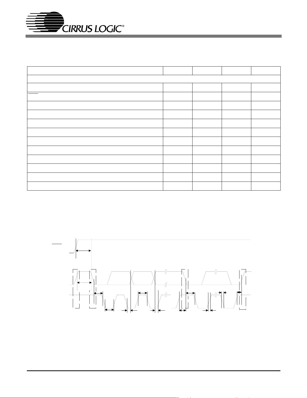
Figure 1. Master Mode Serial Audio Port Timing
t
t
sdo
slr
t
sclkh
t
sclkw
t
sdih
t
sclkl
t
sdis
SDIN
Figure 2. Slave Mode Serial Audio Port Timing
DS593F1 19
t
sdih
Page 20

CS4272
LRCK
Left Channel
SCLK
SDATA +3 +2 +1
MSB
-1 -2 -3 -4 -5
+5 +4
Figure 3. Format 0, Left Justified up to 24-Bit Data
LRCK
SCLK
SDATA +3 +2 +1
MSB
-1 -2 -3 -4 -5
Left Channel
+5 +4
Figure 4. Format 1, I²S up to 24-Bit Data
LRCK
SCLK
Left Channel
LSB
LSB
MSB
-1 -2 -3 -4
MSB
-1 -2 -3 -4
Right Channel
+3 +2 +1
+5 +4
Right Channel
+3 +2 +1
+5 +4
Right Channel
LSB
LSB
SDATA
+6
+4 +3 +2
LSB +5
MSB-1-2-3-4-5
32 clocks
-6
+5
+1 LSB
MSB - 1 - 2 -3 - 4
-5
-6
+6
Figure 5. Format 2, Right Justified 16-Bit Data. (Available in Control Port Mode only)
Format 3, Right Justified 24-Bit Data. (Available in Control Port Mode only)
Format 4, Right Justified 20-Bit Data. (Available in Control Port Mode only)
Format 5, Right Justified 18-Bit Data. (Available in Control Port Mode only)
+4 +3 +2
+1 LSB
20 DS593F1
Page 21
SWITCHING CHARACTERISTICS - I²C MODE CONTROL PORT
(Inputs: logic 0 = AGND, logic 1 = VL)
Parameter Symbol Min Max Unit
I²C Mode
SCL Clock Frequency.
Rising Edge to Start.
RST
Bus Free Time Between Transmissions.
Start Condition Hold Time (prior to first clock pulse).
Clock Low time.
Clock High Time.
Setup Time for Repeated Start Condition.
SDA Hold Time from SCL Falling. (Note 23)
SDA Setup time to SCL Rising.
Rise Time of Both SDA and SCL Lines.
Fall Time of Both SDA and SCL Lines.
Setup Time for Stop Condition.
f
scl
t
irs
t
buf
t
hdst
t
low
t
high
t
sust
t
hdd
t
sud
t
susp
t
r
t
f
-100KHz
500 - ns
4.7 - µs
4.0 - µs
4.7 - µs
4.0 - µs
4.7 - µs
0-µs
250 - ns
-1µs
-300ns
4.7 - µs
CS4272
Notes: 23. Data must be held for sufficient time to bridge the 300 ns transition time of SCL.
RST
t
SDA
SCL
irs
Stop Start
t
buf
t
hdd
t
high
t
sud
t
hdst
t
low
Figure 6. I²C Mode Control Port Timing
Repeated
Start
t
sust
t
hdst
t
f
t
r
Stop
t
susp
DS593F1 21
Page 22

SWITCHING CHARACTERISTICS - SPI CONTROL PORT
(Inputs: logic 0 = AGND, logic 1 = VL)
Parameter Symbol Min Max Unit
SPI Mode
CCLK Clock Frequency.
Rising Edge to CS Falling.
RST
CCLK Edge to CS
High Time Between Transmissions.
CS
Falling to CCLK Edge.
CS
Falling. (Note 24)
CCLK Low Time.
CCLK High Time.
CDIN to CCLK Rising Setup Time.
CCLK Rising to DATA Hold Time. (Note 25)
Rise Time of CCLK and CDIN. (Note 26)
Fall Time of CCLK and CDIN. (Note 26)
f
sclk
t
t
t
t
t
t
sch
t
dsu
t
t
srs
spi
csh
css
scl
dh
r2
t
f2
-6MHz
500 - ns
500 - ns
1.0 - µs
20 - ns
82 - ns
82 - ns
40 - ns
15 - ns
-100ns
-100ns
CS4272
Notes: 24. t
25. Data must be held for sufficient time to bridge the transition time of CCLK.
26. For F
only needed before first falling edge of CS after RST rising edge. t
spi
< 1 MHz
SCK
RST
CS
CCLK
CDIN
t
srs
t
t
css
spi
t
r2
t
t
sch
scl
t
f2
t
t
dsu
dh
= 0 at all other times.
spi
t
csh
Figure 7. SPI Control Port Timing
22 DS593F1
Page 23

4. TYPICAL CONNECTION DIAGRAM
* Only one must be used. See
"Grounding and Power Supply
Decoupling."
∗
Not to exceed 1 µF.
47 µF 0.1 µF
∗
1 µF 0.1 µF
FILT+
AGND
VCOM
5.1 Ω
*
CS4272
+5 V
1 µF0.1 µF
1 µF0.1 µF
+5 V to 3.3 V
VDVA
¤ See "Master/Slave Mode Selection".
VL
¤
*
+5 V to 2.5 V
1 µF0.1 µF
47 kΩ
Power Down
and Mode
Settings
(Control Port)
Analog Input
Buffer
40 pF
40 pF
**
** Optional. See "Crystal
Applications (XTI/XTO)".
)LJ(I2S/ CS / AD0
SDA / CDIN (M1)
)S(M/ SDOUT
SDIN
SCL / CCLK (M0)
RST
MCLK
CS4272
AINA+
SCLK
LRCK
AINAAINB+
AINB-
AOUTA-
AMUTEC
AOUTA+
XTI
AOUTB-
BMUTEC
XTO
AOUTB+
DGND
Figure 8. CS4272 Typical Connection Diagram
Audio Data
Processor
Timing Logic
&
Clock
Analog Conditioning
&
Mute
DS593F1 23
Page 24

CS4272
5. APPLICATIONS
5.1 Stand-Alone Mode
5.1.1 Recommended Power-Up Sequence
1) When using the CS4272 with an external MCLK, hold RST low until the power supply, MCLK, and LRCK are
stable. When using the CS4272 with internally generated MCLK, hold RST
2) Bring RST
the release of RST
high. If the internally generated MCLK is being used, it will appear on the MCLK pin prior to 1 ms from
.
5.1.2 Master/Slave Mode
The CS4272 supports operation in either Master Mode or Slave Mode.
In Master Mode, LRCK and SCLK are outpu ts and are sy nchronously generated on-chip. LRCK is equal to Fs and
SCLK is equal to 64x Fs.
In Slave Mode, LRCK and SCLK are inputs, requiring external generation that is synchronous to MCLK. It is recom-
mended that SCLK be 64x Fs to maximize system performance.
In Stand-Alone Mode, the CS4272 will default to Slave Mode. Master Mode may be accessed by placing a 47 kΩ
pull-up to VL on the SDOUT (M/S
Configuration of clock ratios in each of these modes will be outlined in the Tables 3 and 4.
) pin.
low until the power supply is stable.
5.1.3 System Clocking
The CS4272 will operate at sampling frequencies from 4 kHz to 200 kHz. This range is divided into three speed
modes as shown in Table 1 below.
Table 1. Speed Modes
Mode Sampling Frequency
Single Speed 4-50 kHz
Double Speed 50-100 kHz
Quad Speed 100-200 kHz
5.1.3.1 Crystal Applications (XTI/XTO)
An external crystal may be used in conjunction with the CS4272 to generate the master clock signal. To accomplish
this, a 20 pF fundamental mode parallel resonant crystal must be connected between the XTI and XTO pins as
shown in the Typical Connection Diagram on page 23. This crystal must oscillate at the frequency shown in Table 2.
In this configuration, MCLK is a bu ffered output and, as shown in the Typical Connection Diagram, nothing other
than the crystal and its load capacitors should be connected to XTI and XTO. The MCLK signal will appear on the
MCLK pin prior to 1 ms from the release of RST
Single Speed 512 x Fs
Double Speed 256 x Fs
Quad Speed 128 x Fs
.
Table 2. Crystal Frequencies
Mode Crystal Frequency
To operate the CS4272 with an externally generated MCLK signal, no crystal should be used, XTI should be connected to ground and XTO should be left unconnected. In this configuration, MCLK is an inpu t and must be driven
externally with an appropriate speed clock.
24 DS593F1
Page 25

CS4272
5.1.3.2 Clock Ratio Selection
Depending on the use of an external crystal, or whether the CS4272 is in Master or Slave Mode, different
MCKL/LRCK and SCLK/LRCK ratios may be used. These ratios are shown in the Tables 3 and 4 below.
Table 3. Clock Ratios - Stand Alone Mode With External Crystal
External Crystal Used, MCLK=Output
Master Mode
MCLK/LRCK SCLK/LRCK LRCK
Single Speed 256 64 Fs
Double Speed 128 64 Fs
Quad Speed 128 64 Fs
Slave Mode
MCLK/LRCK SCLK/LRCK LRCK
Single Speed 256 32, 64, 128 Fs
Double Speed 128 32, 64 Fs
Quad Speed 128 32, 64 Fs
Table 4. Clock Ratios - Stand Alone Mode Without External Crystal
External Crystal Not Used, MCLK=Input
Master Mode
MCLK/LRCK SCLK/LRCK LRCK
Single Speed 256 64 Fs
Double Speed 128 64 Fs
Quad Speed 64 32 Fs
Slave Mode
MCLK/LRCK SCLK/LRCK LRCK
256 32, 64, 128 Fs
Single Speed
Double Speed
Quad Speed
384 32, 48, 64, 96, 128 Fs
512 32, 64, 128 Fs
128 32, 64 Fs
192 32, 48, 64 Fs
256 32, 64 Fs
64 32 Fs
96 48 Fs
128 32, 64 Fs
DS593F1 25
Page 26

CS4272
5.1.4 16-Bit Auto-Dither
The CS4272 will auto-configure to output properly dithered 16-bit data when placed in Slave Mode and a 32x SCLK
to LRCK ratio is used. In this configu ration, one half of a bit of dither is added to the LSB of the 16-bit word. This
applies only to the serial audio output of the ADC and will not affect DAC performance. See Figure 9.
16 -B it Wo rd
1514131211109876543210
½ Bit Dith e r
Figure 9. ADC 16-Bit Auto-Dither
5.1.5 Auto-Mute
The DAC output will mute following the reception of 8192 consecutive audio samples of static 0 or -1. A single sample of non-static data will release the mute. Detection and muting are done independently for each channel. The
common mode on the output will be retained and the Mute Control pin for that channel will go active during the mute
period.
5.1.6 High Pass Filter
The operational amplifiers in the input circuitry driving the CS4272 may generate a small DC offset into the ADC.
The CS4272 includes a high pass filter after the decimator to remove any DC offset which could result in recording
a DC level, possibly yielding "clicks" when switching between devices in a multichannel system.
In Stand-Alone Mode, the high pass filter continuously subtracts a measure of the DC offset from the output of the
decimation filter. This function cannot be disabled in Stand-Alone Mode.
5.1.7 Interpolation Filter
In Stand-Alone Mode, the fast roll-off interpolation filter is used.
Filter specifications can be found in Section 3. Plots of the data are contained in the “Appendix” on page 47.
5.1.8 Mode Selection & De-Emphasis
The sample rate, Fs, can be adjusted from 4 kHz to 200 kHz. In Stand-Alone Mode, the CS4272 must be set to the
proper mode via the mode pins, M1 and M0. De-emphasis, optimized for a 44.1 kHz sampling frequency, is available.
Table 5. CS4272 Stand-Alone Mode Control
Mode 1 Mode 0 Mode Sample Rate (Fs) De-Emphasis
0 0 Single Speed Mode 4 kHz - 50 kHz 44.1 kHz
0 1 Single Speed Mode 4 kHz - 50 kHz Off
1 0 Double Speed Mode 50 kHz - 100 kHz Off
1 1 Quad Speed Mode 100 kHz - 200 kHz Off
5.1.9 Serial Audio Interface Format Selection
Either I2S or left justified serial audio data format may be selected in Stand-Alone Mode. The selection will affect
both the input and output format. Placing a 10 kΩ pull-up to VL on the I2S/LJ
placing a 10 kΩ pull-down to DGND on the I2S/LJ
26 DS593F1
pin will select the left justified format.
pin will select the I2S format, while
Page 27
CS4272
5.2 Control Port Mode
5.2.1 Recommended Power-Up Sequence - Access to Control Port Mode
1) When using the CS4272 with an external MCLK, hold RST low until the power supply, MCLK, and LRCK are
stable. When using the CS4272 with internally generated MCLK, hold RST
In this state, the Control Port is reset to its default settings.
2) Bring RST
generated MCLK is being used, it will appear on the MCLK pin prior to 1 ms from the release of RST
3) Write 03h to register 07h within 10 ms following the release of RST
and Power Down (PDN) bits, activating the Control Port and placing the part in power-down. When using the
CS4272 with internally generated MCLK, it is necessary to wait 1 ms following the release of RST
ating this Control Port write.
4) The desired register settings can be loaded while keeping the PDN bit set.
5) Clear the PDN bit to initiate the power-up sequence. This power-up se quence requires approximately 85 µS.
high. The device will remain in a low power state and the control port will be accessible. If internally
. This sets the Control Port Enable (CPEN)
5.2.2 Master / Slave Mode Selection
The CS4272 supports operation in either Master Mode or Slave Mode.
In Master Mode, LRCK and SCLK are outpu ts and are sy nchronously generated on-chip. LRCK is equal to Fs and
SCLK is equal to 64x Fs.
In Slave Mode, LRCK and SCLK are inputs, requiring external generation that is synchronous to MCLK. It is recom-
mended that SCLK be 64x Fs to maximize system performance.
Configuration of clock ratios in each of these modes will be outlined in the Tables 8 and 9.
In Control Port Mode the CS4272 will default to Slave Mode. The user may change this default setting by changing
the status of the M/S
bit in the Mode Control 1 register (01h).
low until the power supply is stable.
.
before initi-
5.2.3 System Clocking
The CS4272 will operate at sampling frequencies from 4 kHz to 200 kHz. This range is divided into three speed
modes as shown in Table 6 below.
Table 6. Speed Modes
Mode Sampling Frequency
Single Speed 4-50 kHz
Double Speed 50-100 kHz
Quad Speed 100-200 kHz
5.2.3.1 Crystal Applications (XTI/XTO)
An external crystal may be used in conjunction with the CS4272 to generate the MCLK signal. To accomplish this,
a 20 pF fundamental mode parallel resonant crystal must be connected betwee n the XTI and XTO pins as shown in
the Typical Connection Diagram on page 23. This crystal must oscillate at the frequency shown in Table 7. In this
configuration, MCLK is a buffered ou tp ut an d, as sh own in the Typical Connection Diagram, nothing other than the
crystal and its load capacitors should be connected to XTI and XTO. The MCLK signal will appear on the MCLK pin
prior to 1 ms from the release of RST
.
DS593F1 27
Page 28

CS4272
Table 7. Crystal Frequencies
Mode Crystal Frequency
Single Speed 512 x Fs
Double Speed 256 x Fs
Quad Speed 128 x Fs
To operate the CS4272 with an externally generated MCLK signal, no crystal should be used, XTI should be connected to ground and XTO should be left unconnected. In this configuration, MCLK is an inpu t and must be driven
externally with an appropriate speed clock.
5.2.3.2 Clock Ratio Selection
Depending on the use of an external crystal, or whether the CS4272 is in Master or Slave Mode, different
MCKL/LRCK and SCLK/LRCK ratios may be used. These ratios as well as the Control Port Register Bits that must
be set in order to obtain them are shown in Tables 8 and 9 below.
Table 8. Clock Ratios - Control Port Mode With External Crystal
External Crystal Used, MCLK=Output
Master Mode
MCLK/LRCK SCLK/LRCK LRC K Ratio1 Bit Ratio0 Bit
Single Speed
256 64 Fs 0 d
512 64 Fs 1 d
Double Speed
128 64 Fs 0 d
256 64 Fs 1 d
Quad Speed
128 64 Fs d
27
Slave Mode
MCLK/LRCK SCLK/LRCK LRC K Ratio1 Bit Ratio0 Bit
Single Speed
256 32, 64, 128 Fs 0 d
512 32, 64, 128 Fs 1 d
Double Speed
128 32, 64 Fs 0 d
256 32, 64 Fs 1 d
Quad Speed
128 32, 64 Fs d
27
Notes: 27. For the Ratio1 and Ratio0 bits listed above, “d” indicates that any value may written.
27
27
27
27
27
d
27
27
27
27
27
d
28 DS593F1
Page 29

Single Speed
Double Speed
Quad Speed
CS4272
Table 9. Clock Ratios - Control Port Mode Without External Crystal
External Crystal Not Used, MCLK=Input
Master Mode
MCLK/LRCK SCLK/LRCK LRCK Ratio1 Bit Ratio0 Bit
256 64 Fs 0 0
384 64 Fs 0 1
512 64 Fs 1 0
768 64 Fs 1 1
128 64 Fs 0 0
192 64 Fs 0 1
256 64 Fs 1 0
384 64 Fs 1 1
64 32 Fs 0 0
96 32 Fs 0 1
128 64 Fs 1 0
192 64 Fs 1 1
Single Speed
Double Speed
Quad Speed
Slave Mode
MCLK/LRCK SCLK/LRCK LRCK Ratio1 Bit Ratio0 Bit
256 32, 64, 128 Fs 0 d
384 32, 48, 64, 96, 128 Fs 0 d
512 32, 64, 128 Fs 0 d
768 32, 48, 64, 96, 128 Fs 1 d
1024 32, 64, 128 Fs 1 d
128 32, 64 Fs 0 d
192 32, 48, 64 Fs 0 d
256 32, 64 Fs 0 d
384 32, 48, 64 Fs 1 d
512 32, 64 Fs 1 d
64 32 Fs 0 d
96 48 Fs 0 d
128 32, 64 Fs 0 d
192 48 Fs 1 d
256 32, 64 Fs 1 d
28
28
28
28
28
28
28
28
28
28
28
28
28
28
28
Notes: 28. For the Ratio0 bit listed above, “d” indicates that any value may written.
DS593F1 29
Page 30

CS4272
5.2.4 Internal Digital Loopback
In Control Port Mode, the CS4272 suppor ts an internal d igital loopback m ode in which the output of th e ADC is routed to the input of the DAC. This mode may be activated by setting the LOOP bit in the Mode Contro l 2 register (07h).
When this bit is set, the status of the DAC_DIF(2:0) bits in register 01h will be disregarded by the CS4272. Any
changes made to the DAC_DIF(2:0) bits while the LOOP bit is set will have no impact on operation until the LOOP
bit is released, at which time the Digital Interface Format of the DAC will operate according to the format selected in
the DAC_DIF(2:0) bits. While the LOOP bit is set, data will be present on the SDOUT pin in the format selected in
the ADC_DIF bit in register 06h.
5.2.5 Dither for 16-Bit Data
The CS4272 may be configured to properly dither for 16-bit data. To do this, the Dither16 bit in the ADC Control
Register (06h) must be set. When set, a half bit of dither is added to the least significant bit of the 16 most significant
bits of the data word. The remaining bits should be disregarded. See Figure 10. This function is useful when 16-bit
devices are downstream of the ADC. This bit should not be set when using word lengths greater than 16 bits.
It should be noted that this function is supported for all serial audio output formats, and may be activated in either
Master or Slave Mode.
16-Bit Word
23 22 21 20 19 18 17 16 15 14 13 12 11 10 9 8 7 6 5 4 3 2 1 0
½ Bit D ither
Figure 10. Example of Dither for 16-Bit Data with 24-Bit Left Justified Format
Disregard Contents
5.2.6 Auto-Mute
The Auto-Mute function is controlled by the status of the AMUTE bit in the DAC Control re gister. When set, the DAC
output will mute following the reception of 8192 consecutive audio samples of static 0 or -1. A single sample of nonstatic data will release the mute. Detection and muting are done independently for each channel. Auto-Mute detection and muting can become dependent on either channel if the MUTECA=B function is enabled. The common mod e
on the output will be retained and the Mute Control pin for that channel will become active during the mute period.
The muting function is effected, similar to volume control changes, by the Soft and ZeroCross bits in the DAC Volume and Mixing Control register. The AMUTE bit is set by default.
5.2.7 High Pass Filter and DC Offset Calibration
The operational amplifiers in the input circuitry driving the CS4272 may generate a small DC offset into the A/D converter. The CS4272 includes a high pass filter after the decimator to remove any DC offset which could result in
recording a DC level, possibly yielding "clicks" when switching between devices in a multichanne l syste m .
The high pass filter continuously subtracts a measure of the DC offset from the output of the decimation filter. The
high pass filter can be independen tly enabled and disabled for chann els A and B. If the HPFDisableA or HPFDis ableB bit is set during normal operation, the current value of the DC offset for the corresponding channel is frozen
and this DC offset will continue to be subtracted from the conversion result. This feature ma kes it possible to perform
a system DC offset calibration by:
1) Running the CS4272 with the high pass filter enabled un til the filter settles. See the Dig ital Filter Characteristics
for filter settling time.
2) Disabling the high pass filter and freezing the stored DC offset.
30 DS593F1
Page 31

CS4272
A system calibration performed in this way will eliminate offsets anywhere in the signal path between the calibration
point and the CS4272.
5.2.8 Interpolation Filter
To accommodate the increasingly complex requirements of digital audio systems, the CS4272 incorporates selectable interpolation filters for each mode of operation. Fast and slow roll-off filters are available in each of Single, Double, and Quad Speed modes. These filters have been designed to accommodate a variety of musical tastes and
styles. The FILT_SEL bit in the DAC Control register (02h) is used to select which filter is used. By default, the fast
roll-off filter is selected.
Filter specifications can be found in Section 3. Plots of the data are contained in the “Appendix” on page 47.
5.2.9 De-Emphasis
Three de-emphasis modes are available via the Control Port. The available filters are optimized for 32 kHz,
44.1 kHz, and 48 kHz sampling rates. See Table 13 for de-emphasis selection in Control Port Mode.
5.2.10 Oversampling Modes
The CS4272 operates in one of three oversampling modes based on the input sample rate. Mode selection is determined by the M1 and M0 bits in the Mode Control 1 register. Single-Speed mode supports input sample rates up
to 50 kHz and uses a 128x oversampling ratio. Double-Spee d mode supports input sample r ates up to 100 k Hz and
uses an oversampling ratio of 64x. Quad-Speed mode supports input sample rates up to 200 kHz and uses an oversampling ratio of 32x. See Table 11 for Control Port Mode settings.
5.3 De-Emphasis Filter
The CS4272 includes on-chip digital de-emphasis. Figure 1 1 shows the de-emphasis curve for Fs equal to 44.1 kHz.
The frequency response of the de-emphasis curve will scale proportionally with changes in sample rate, Fs. Please
see section 5.1.8 for the desired de-emphasis control for Stand-Alone mode and section 5.2.9 for control port mode.
The de-emphasis feature is included to accommodate audio recordings that utilize 50/15 µS pre-emphasis equalization as a means of noise reduction.
De-emphasis is only available in Single Speed Mode.
Gain
dB
T1=50 µs
0dB
T2 = 15 µs
-10dB
F1 F2
3.183 kHz 10.61 kHz
Figure 11. De-Emphasis Curve
Frequency
DS593F1 31
Page 32
CS4272
5.4 Analog Connections
5.4.1 Input Connections
The analog modulator samples the input at 6.144 MHz (MCLK=12.288 MHz). The digital filter will reject signals within the stopband of the filter. However, there is no rejection for input signals which are (n
passband frequency, where n=0,1,2,... Refer to Figure 12 for a recommended analog input buffer that will attenuate
any noise energy at 6.144 MHz, in addition to providing the optimum source impe dance for the modulators. The use
of capacitors which have a larg e voltage coefficient (such as general pu rpose ceramics) must be avoided since
these can degrade signal linearity. Figure 13 shows the full-scale analog input levels.
634 Ω
× 6.144 MHz) the digital
AIN+
AIN-
10 µF
10 kΩ
10 kΩ
10 µF
470 pF
C0G
-
+
470 pF
0.01 µF
Figure 12. CS4272 Recommended Analog Input Buffer
C0G
-
+
91 Ω
634 Ω
91 Ω
1 µF
3.9 V
2.5 V
1.1 V
3.9 V
CS4272
AIN+
2700 pF
C0G
AIN-
VCOM
0.1 µF
CS4272
AIN+
2.5 V
AIN-
1.1 V
Full-Scale Input Level= (AIN+) - (AIN-)= 5.6 Vpp
Figure 13. Full-Scale Analog Input
32 DS593F1
Page 33

CS4272
5.4.2 Output Connections
The recommended output filter configuration is shown in Figure 14 . This filter configuration accounts for the normally
differing AC loads on the AOUT+ and AOUT- differential output pins. It also shows an AC coupling configuration
which minimizes the number of required AC coupling capacitors.
The CS4272 does not include phase or amplitude compensation for an external filter, and therefore the DAC system
phase and amplitude response will be dependent on the external analog circuitry. Figure 15 shows the full-scale analog output levels.
CS4272
AOUT-
AOUT+
2200 pF
C0G
4.42 kΩ
1.33 kΩ
6.8 nF
C0G
Figure 14. CS4272 Recommended Analog Output Filter
CS4272
AOUT+
2.32 kΩ
715 Ω
1.50 kΩ
4.99 kΩ
-
+
22 µF
470 pF
C0G
1.5 nF
C0G
22 µF
560 Ω
47 kΩ
3.75 V
2.5 V
1.25 V
3.75 V
Analog
Out
AOUT-
Full-Scale Output Level= (AIN+) - (AIN-)= 5 Vpp
Figure 15. Full-Scale Analog Output
DS593F1 33
2.5 V
1.25 V
Page 34

CS4272
5.5 Mute Control
The Mute Control pins become active during power-up initialization, reset, muting, if the MCLK to LRCK ratio is incorrect, and during power-down. The Auto-Mute function causes the MUTEC pin corresponding to an individual
channel to activate following the reception of 8192 consecutive audio samples of static 0 or -1 on the respective
channel. A single sample of non-zero data on this channel will cause the MUTEC pin to deactivate. In Control Port
Mode, however, auto-mute detection and muting can becom e dependent on eithe r channel if the MuteB=A function
is enabled. The MUTEC pins are intended to be used as control for an external mute circuit in order to add off-chip
mute capability.
Use of the Mute Control function is not mandatory but recommended for designs requiri ng the a bsolute m inimum in
extraneous clicks and pops. Also, use of the Mute Control function can enable the system designer to achieve idle
channel noise/signal-to-noise ratios which are only limited by the external mute circuit. The MUTEC pins are activelow. See Figure 16 below for a suggested active-low mute circuit.
+V
EE
AOUT
CS4272
MUTEC
LPF
AC
Couple
-V
EE
+V
MMUN2111LT1
560 Ω
A
2 kΩ
10 kΩ
-V
EE
Audio
47 kΩ
Out
Figure 16. Suggested Active-Low Mute Circuit
5.6 Synchronization of Multiple Devices
In systems where multiple ADCs are required, care must be taken to achieve simultaneous sampling. To ensure
synchronous sampling, the MCLK and LRCK must be the same for all of the CS4272’s in the syste m. If only one
MCLK source is needed, one solution is to place one CS4272 in Master Mode, and slave all of the other CS4272’s
to the one master. If multiple MCLK sources are needed, a possible solution would be to supply all clocks from the
same external source and time the CS4272 reset with the inactive edge of MCLK. This will ensure that all converters
begin sampling on the same clock edge.
5.7 Grounding and Power Supply Decoupling
As with any high resolution converter, the CS4272 requires careful attention to power supply and grounding arrangements if its potential performance is to be realized. Figure 8 shows the recommended power arrangements, with VA
and VL connected to clean supplies. VD, which powers the digital filter, may be run from the system logic supply
(VL) or may be powered from the analog supply (VA) via a resistor. In this case, no additional devices should be
powered from VD. Power supply decoupling capacitors should be as near to the CS4272 as possible, with the low
value ceramic capacitor being the nearest. All signals, especially clocks, should be kept away from the VREF and
VCOM pins in order to avoid unwanted coupling into the mod ulators . T he VREF and VCOM de co upling cap acitors,
particularly the 0.1 µF, must be positioned to minimize the electrical path from VREF and AGND. The CDB4272
evaluation board demonstrates the optimum layout and power supp ly arrangements. To minimi ze digital noise, connect the CS4272 digital outputs only to CMOS inputs.
34 DS593F1
Page 35

CS4272
6. CONTROL PORT INTERFACE
The Control Port is used to load all the internal settings of the CS4272. The operation of the Control Port may be
completely asynchronous to the audio sample rate. However, to avoid potential interference problems, the Control
Port pins should remain static if no operation is required.
The Control Port has 2 modes: SPI and I²C, with the CS4272 operating as a slave to control messages in both
modes. If I²C operation is desired, AD0/CS
transition on AD0/CS
after power-up, SPI mode will be selected. The Control Port registers are write-only in SPI
mode.
Upon release of the RST
pin, the CS4272 will wait approximately 10 ms before it begins its start-up sequence. The
part defaults to Stand-Alone Mode, in which a ll opera tional modes are controlled as described under “Stand-Alone
Mode” on page 24. The Control Port is active at all times, and if bit 1 of register 07h (CPEN) is set, the part enters
Control-Port Mode and all operational modes are controlled by the Control Port registers. This bit can be set at any
time, but to avoid unpredictable output noises, bit 1 (CPEN) and bit 0 (PDN) of register 07h should be set by writing
03h before the end of the 10 ms start-up wait period. All registers can then be set as desired before releasing the
PDN bit to begin the start-up sequence. If system requirements do not allow writing to the control port immediately
following the release of RST
, the SDIN line should be held at logic “0” until the proper serial mode can be selected.
6.1 SPI Mode
In SPI mode, CS is the CS4272 chip select signal, CCLK is the control port bit clock, CDIN is the input data line from
the microcontroller and the chip address is 0010000. All control signals are inputs and data is clocked in on the rising
edge of CCLK.
Figure 17 shows the operation of the Control Port in SPI mode. To write to a register, bring CS
on CDIN form the chip address, and must be 0010000. The eighth bit is a read/write indicator (R/W
low to write. The next 8 bits form the Memory Address Pointer (MAP), which is set to the address of the register that
is to be updated. The next 8 bits are the data which will be placed into the register designated by the MAP. See
Table 10 on page 36.
should be tied to VA or AGND. If the CS4272 ever detects a high to low
low. The first 7 bits
), which must be
CS
CCLK
CHIP
ADDRESS
CDIN
0010000
MAP = Memory Address Pointer
Figure 17. Control Port Timing, SPI mode
R/W
MAP
MSB
byte 1
DATA
LSB
byte n
The CS4272 has MAP auto increment capability, enabled by the INCR bit in the MAP. If INCR is 0, then the MAP
will stay constant for successive writes. If INCR is set, then MAP will auto increment after each byte is written, allowing block writes to successive registers.
DS593F1 35
Page 36

CS4272
6.2 I²C Mode
In
I²C
mode, SDA is a bi-directional data line. Data is clocked into and out o f the part by the clock, SC L, with the clock
to data relationship as shown in Fi gu re 1 8. Th ere is no CS
tied to VA or AGND as required. The upper 6 bits of the 7- b it address field mus t be 001 000 . To c ommunic ate with the
CS4272
,
the LSB of the chip address field, which is the first byte sent to the CS4272, should match the setting of the
AD0 pin. The eighth bit of the address byte is the R/W
the next byte is the Memory Address Pointer, MAP, which selects the register to be read or written. The MAP is then
followed by the data to be written. If the operation is a read, th en the contents of the register pointed to by the MAP will
be output after the chip address.
The CS4272 has MAP auto increment capability, enabled by the INCR bit in the MAP. If INCR is 0, then the MAP
will stay constant for successive writes. If INCR is set, then MAP will auto increment after each byte is written, allowing block reads or writes of successive registers.
SDA
SCL
001000
ADDR
AD0
R/W
pin. Pin AD0 forms the partial chip address and should be
bit (high for a read, low for a write). If the operation is a write,
Note 1
ACK
DATA
1-8
ACK
DATA
1-8
ACK
Start
Note: If operation is a write, this byte contains the Memory Address Pointer, MAP.
Figure 18. Control Port Timing, I²C Mode
Stop
Table 10. Memory Address Pointer (MAP)
76543210
INCR Reserved Reserved Reserved MAP3 MAP2 MAP1 MAP0
00000000
INCR - Auto MAP Increment Enable
Default = ‘0’.
0 - Disabled
1 - Enabled
MAP(3:0) - Memory Address Pointer
Default = ‘0000’.
36 DS593F1
Page 37

CS4272
7. REGISTER QUICK REFERENCE
This table shows the register names and their associated default values.
Addr Function 7 6 5 4 3 2 1 0
01h Mode Control 1
02h DAC Control AMUTE FILT_SEL DEM1 DEM0 RMP_UP RMP_DN INV_B INV_A
03h DAC Volume &
Mixing Control
04h DAC Ch A Vol-
ume Control
05h DAC Ch B Vol-
ume Control
06h ADC Control Reserved Reserved Dither16 ADC_DIF0 MUTEA MUTEB HPFDisableA HPFDisableB
07h Mode Control 2 Reserved Reserved Reserved LOOP MUTECA=B F REEZE CPEN PDN
08h Chip ID PART3 PART2 PART1 PART0 REV3 REV2 REV1 REV0
M1 M0 Ratio1 Ratio0
000 0 0 0 0 0
100 0 0 0 0 0
Reserved B=A Soft ZeroCross ATAPI3 ATAPI2 ATAPI1 ATAPI0
001 0 1 0 0 1
MUTE VOL6 VOL5 VOL4 VOL3 VOL2 VOL1 VOL0
000 0 0 0 0 0
MUTE VOL6 VOL5 VOL4 VOL3 VOL2 VOL1 VOL0
000 0 0 0 0 0
000 0 0 0 0 0
000 0 0 0 0 0
000 0 0 0 0 0
M/S
DAC_DIF2 DAC_DIF1 DAC_DIF0
DS593F1 37
Page 38

CS4272
8. REGISTER DESCRIPTION
** All registers are read/write in I²C mode and write only in SPI mode, unless otherwise noted**
8.1 Mode Control 1 - Address 01h
76543210
M1 M0 Ratio1 Ratio0 M/S
8.1.1 Functional Mode (Bits 7:6)
Function:
Selects the required range of input sample rates.
Table 11. Functional Mode Selection
M1 M0 Mode
0 0 Single-Speed Mode: 4 to 50 kHz sample rates (default)
0 1 Single-Speed Mode: 4 to 50 kHz sample rates
1 0 Double-Speed Mode: 50 to 100 kHz sample rates
1 1 Quad-Speed Mode: 100 to 200 kHz sample rates
DAC_DIF2 DAC_DIF1 DAC_DIF0
8.1.2 Ratio Select (Bits 5:4)
Function:
These bits are used to select the clocking ratios in Control Port Mode. Please refe r to Table 8, “Clock
Ratios - Control Port Mode With External Crystal,” on page 28 or Table 9, “Clock Ratios - Control Port
Mode Without External Crystal,” on page 29 for information on which of these bits to set to obtain specific clock ratios.
8.1.3 Master / Slave Mode (Bit 3)
Function:
This bit selects either master or slave operation. Setting this bit will select master mode, while clearing
this bit will select slave mode.
8.1.4 DAC Digital Interface Format (Bits 2:0)
Function:
The required relationship between LRCK, SCLK and SDIN for the DAC is defined by the DAC Digital
Interface Format and the options are detailed in Table 12 and Figures 3-5.
Table 12. DAC Digital Interface Formats
DAC_DIF2 DAC_DIF1 DAC_DIF0 Description Format Figure
0 0 0 Left Justified, up to 24-bit data (default) 0 3
001
0 1 0 Right Justified, 16-bit Data 2 5
0 1 1 Right Justified, 24-bit Data 3 5
1 0 0 Right Justified, 20-bit Data 4 5
1 0 1 Right Justified, 18-bit Data 5 5
110 Reserved
111 Reserved
2
I
S, up to 24-bit data
14
38 DS593F1
Page 39
CS4272
8.2 DAC Control - Address 02h
76543210
AMUTE FILT_SEL DEM1 DEM0 RMP_UP RMP_DN INV_A INV_B
8.2.1 Auto-Mute (Bit 7)
Function:
When set, enables the Auto-Mute function. See “Auto-Mute” on page 30.
8.2.2 Interpolation Filter Select (Bit 6)
Function:
This Function allows the user to select whether the Interpolation Filter has a fast or slow roll off. When
set, this bit selects the slow roll off filter, when cleared it selects the fast roll off filter. The - 3 dB corner
is approximately the same for both filters, but the slope of the roll off is greater for the fast r oll off filter.
8.2.3 De-Emphasis Control (Bits 5:4)
Function:
Implementation of the standard 50/15 µs digital de-emphasis filter response, Figure 19, requires reconfiguration of the digital filter to maintain the proper filter response for 32, 44.1 or 48 kHz sample
rates. NOTE: De-emphasis is available only in Single-Speed Mode. See Table 13 below.
Table 13. De-Emphasis Mode Selection
DEM1 DEM0 Description
0 0 Disabled (default)
0 1 44.1 kHz de-emphasis
1 0 48 kHz de-emphasis
1 1 32 kHz de-emphasis
Gain
dB
T1=50 µs
0dB
T2 = 15 µs
-10dB
F1 F2
3.183 kHz 10.61 kHz
Figure 19. De-Emphasis Curve
Frequency
DS593F1 39
Page 40

8.2.4 Soft Volume Ramp-Up After Error (Bit 3)
Function:
An un-mute will be performed after executing a filter mode change, after a MCLK/LRCK ratio change
or error, and after changing the Functional Mode. When this bit is set, this un-mute is effected, similar
to attenuation changes, by the Soft and ZeroCross bits in the DAC Volume & Mixing Control register.
When cleared, an immediate un-mute is performed in these instances.
Note: For best results, it is recommended that this feature be used with the RMP_DN bit.
8.2.5 Soft Ramp-Down Before Filter Mode Change (Bit 2)
Function:
A mute will be performed prior to executing a filter mode change. When this bit is set, this mute is
effected, similar to attenuation changes, by the Soft and ZeroCross bits in the DAC Volume & Mixing
Control register. When cleared, an immediate mute is performed prior to executing a filter mode
change.
Note: For best results, it is recommended that this feature be used in conjunction with the RMP_UP
bit.
8.2.6 Invert Signal Polarity (Bits 1:0)
CS4272
Function:
When set, this bit activates an inversion of the signal polarity for the appropriate chann el. This is useful if a board layout error has occurred, or other situations where a 180 degree phase shift is de sirable.
8.3 DAC Volume & Mixing Control - Address 03h
76543210
Reserved B=A Soft ZeroCross ATAPI3 ATAPI2 ATAPI1 ATAPI0
8.3.1 Channel B Volume = Channel A Volume (Bit 6)
Function:
The AOUTA and AOUTB volume levels are independ ently controlled by the A an d the B Channel Volume Control Bytes when this function is disabled. The volume on both AOUTA and AOUTB are determined by the A Channel Volume Control Byte and the B Channel Byte is ignored when this function
is enabled. Volume and muting functions are effected by the Soft Ramp an d ZeroCross functions below.
8.3.2 Soft Ramp or Zero Cross Enable (Bits 5:4)
Function:
Soft Ramp Enable
Soft Ramp allows level changes, both muting and attenuation, to be implemented by incrementally
ramping, in 1/8 dB steps, from the current level to the new level at a r ate of 1 d B per 8 left/right clock
periods. See Table 14 on page 41.
Zero Cross Enable
Zero Cross Enable dictates that signal level changes, either by attenuation changes or muting, will
occur on a signal zero crossing to minimize audible artifacts. The requested level change will occur
after a time-out period between 512 and 1 024 sample periods ( 10.7 ms to 21.3 ms at 48 kHz sample
rate) if the signal does not encounter a ze ro cro s sing. The ze ro cross functi on is independ ently mon-
40 DS593F1
Page 41
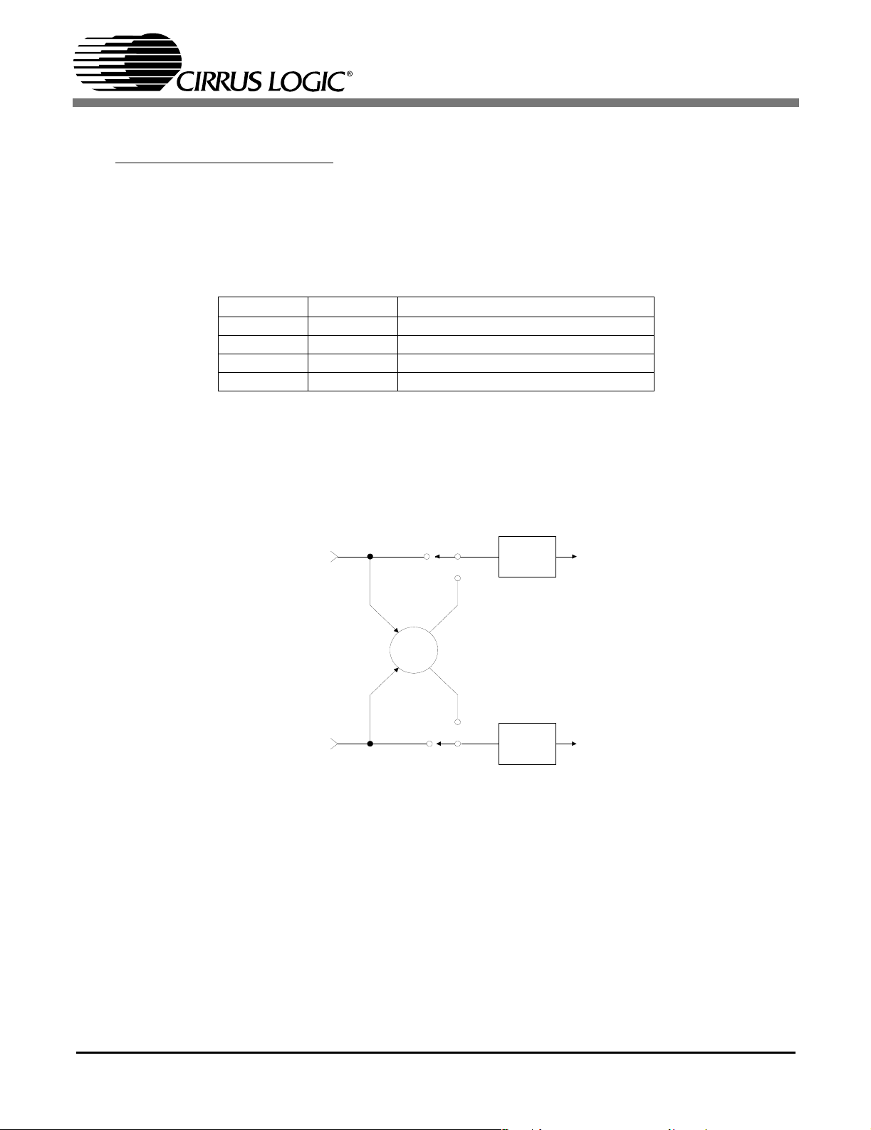
itored and implemented for each channel. See Table 14 on page 41.
Soft Ramp and Zero Cross Enable
Soft Ramp and Zero Cross Enable dictate that signal level ch anges, either by attenuation changes or
muting, will occur in 1/8 dB steps and be implemented on a signal zero crossing. The 1/8 dB level
change will occur after a time-out period between 51 2 and 1024 sample per iods (10.7 ms to 2 1.3 ms
at 48 kHz sample rate) if the signal does not encounter a zero crossing. The ze ro cross function is
independently monitored and implemented for each channel. See Table 14 on page 41.
Table 14. Soft Cross or Zero Cross Mode Selection
Soft ZeroCross Mode
0 0 Changes to affect immediately
0 1 Zero Cross enabled
1 0 Soft Ramp enabled (default)
1 1 Soft Ramp and Zero Cross enabled
8.3.3 ATAPI Channel Mixing and Muting (Bits 3:0)
Function:
The CS4272 implements the channel mixing functions of the ATAPI CD-ROM specification. See
Table 15 on page 42
CS4272
Left Channel
Audio Data
Right Channel
Audio Data
A Channel
Volume
Control
Σ
B Channel
Volume
Control
Figure 20. ATAPI Block Diagram
AoutA
AoutB
DS593F1 41
Page 42

CS4272
ATAPI3 ATAPI2 ATAPI1 ATAPI0 AOUTA AOUTB
0000 MUTE MUTE
0001 MUTE bR
0010 MUTE bL
0 0 1 1 MUTE b[(L+R)/2]
0100 aR MUTE
0101 aR bR
0110 aR bL
0 1 1 1 aR b[(L+R)/2]
1000 aL MUTE
1001 aL bR
1010 aL bL
1 0 1 1 aL b[(L+R)/2]
1100 a[(L+R)/2] MUTE
1101 a[(L+R)/2] bR
1110 a[(L+R)/2] bL
1 1 1 1 a[(L+R)/2] b[(L+R)/2]
Table 15. ATAPI Decode
8.4 DAC Channel A Volume Control - Address 04h
See 8.5 DAC Channel B Volume Control - Address 05h
8.5 DAC Channel B Volume Control - Address 05h
76543210
MUTE VOL6 VOL5 VOL4 VOL3 VOL2 VOL1 VOL0
8.5.1 Mute (Bit 7)
Function:
The DAC output will mute when this bit is set. Though this bit is active high, it should be noted that
the MUTEC pins are active low. The common mode voltage on the output will be retained when this
bit is set. The muting function is effected, similar to attenuation changes, by the Soft and ZeroCross
bits in the Volume and Mixing Control register. The MUTEC pin for the respective channel will become
active during the mute period if the MUTE bit is set. Both the AMUTEC and BMUTEC will become
active if either MUTE register is enabled and the MUTECB=A bit (register 7) is enabled.
8.5.2 Volume Control (Bits 6:0)
Function:
The digital volume control allows the user to attenuate the signal in 1 dB increments from 0 to -127 dB.
Volume settings are decoded as shown in Table 16. The volume changes are imple mented as dictated by the Soft and ZeroCross bits in the DAC Volume & Mixing Control register (see section 8.3.2).
Table 16. Digital Volume Control Example Settings
Binary Code Decimal Value Volume Setting
0000000 0 0 dB
0010100 20 -20 dB
0101000 40 -40 dB
0111100 60 -60 dB
1011010 90 -90 dB
42 DS593F1
Page 43
CS4272
8.6 ADC Control - Address 06h
76543210
Reserved Reserved Dither16 ADC_DIF MUTEA MUTEB HPFDisableA HPFDisableB
8.6.1 Dither for 16-Bit Data (Bit 5)
Function:
When set, this bit activates the Dither for 16-Bit Data feature as described in “Dither for 16-Bit Data”
on page 30.
8.6.2 ADC Digital Interface Format (Bit 4)
Function:
The required relationship between LRCK, SCLK and SDOUT for the ADC is defined by the ADC Digital Interface Format. The options are detailed in Table 17 and may be seen in Figure 3 and 4.
Table 17. ADC Digital Interface Formats
ADC_DIF Description Format Figure
0 Left Justified, up to 24-bit data (default) 0 3
1
2
I
S, up to 24-bit data
14
8.6.3 ADC Channel A & B Mute (Bits 3:2)
Function:
When this bit is set, the output of the ADC for the selected channel will be muted.
8.6.4 Channel A & B High Pass Filter Disable (Bits 1:0)
Function:
When this bit is set, the internal high-pass filter for the selected channel will be disabled.The current
DC offset value will be frozen and continue to be subtracted from the conversion result. See “High
Pass Filter and DC Offset Calibration” on page 30.
8.7 Mode Control 2 - Address 07h
76543210
Reserved Reserved Reserved LOOP MUTECA=B FREEZE CPEN PDN
8.7.1 Digital Loopback (Bit 4)
Function:
When this bit is set, an internal digital loopback from the ADC to the DAC will be enabled. Please refer
to “Internal Digital Loopback” on page 30.
8.7.2 AMUTEC = BMUTEC (Bit 3)
Function:
When this function is enabled, the individual controls for AMUTEC and BMUTEC are internally connected through an AND gate prior to the output pins. Therefore, the external AMUTEC and BMUTEC
pins will go active only when the requirements for both AMUTEC and BMUTEC are valid.
DS593F1 43
Page 44

8.7.3 Freeze (Bit 2)
Function:
This function allows modifications to the control port registers without the changes taking effect until
FREEZE is disabled. To make multiple changes in the Control Port registers take effect simultaneously, set the FREEZE bit, make all register changes, then clear the FREEZE bit.
8.7.4 Control Port Enable (Bit 1)
Function:
This bit is cleared by default, allowing the device to power-up in Stand-Alone Mode. Control Por t
Mode can be accessed by setting this bit. This will allow the operation of the device to be controlled
by the registers and the pin definitions will conform to Control Port Mode. See “Recommended PowerUp Sequence - Access to Control Port Mode” on page 27.
8.7.5 Power Down (Bit 0)
Function:
The device will enter a low-power state whenever this bit is set. The power-down bit is set by default
and must be cleared before normal operation in Control Port Mode can occur. The contents of the
control registers are retained when the device is in power-down.
CS4272
8.8 Chip ID - Register 08h
B7 B6 B5 B4 B3 B2 B1 B0
PART3 PART2 PART1 PART0 REV3 REV2 REV1 REV0
This is a Read-Only register.
8.8.1 Chip ID (Bits 7:4)
Function:
Chip ID code for the CS4272. Permanently set to 0000b (0h).
8.8.2 Chip Revision (Bits 3:0)
Function:
Chip Revision code for the CS4272.
Revision A is coded as 0000b (0h).
Revision B is coded as 0000b (0h).
44 DS593F1
Page 45

9. PARAMETER DEFINITIONS
Dynamic Range
The ratio of the rms value of the signal to the rms sum of all other spectral components over the specified
bandwidth. Dynamic Range is a signal-to-noise ratio measurement over the specified bandwidth made
with a -60 dBFS signal. 60 dB is added to resulting measurement to refer the measurement to full-scale.
This technique ensures that the distortion components are below the noise level and do not affect the
measurement. This measurement technique has been accepted by the Audio Engineering Society,
AES17-1991, and the Electronic Industries Association of Japan, EIAJ CP-307. Expressed in decibels.
Total Harmonic Distortion + Noise
The ratio of the rms value of the signal to the rms sum of all other spectral components over the specified
bandwidth (typically 10 Hz to 20 kHz), including distortion components. Expressed in decibels. Measured
at -1 and -20 dBFS as suggested in AES17-1991 Annex A.
Frequency Response
A measure of the amplitude response variation from 10 Hz to 20 kHz relative to the amplitude response
at 1 kHz. Units in decibels.
Interchannel Isolation
A measure of crosstalk between the left and right channels. Measured for each channel at the conver ter's
output with no signal to the input under test and a full-scale signal applied to the other channel. Units in
decibels.
Interchannel Gain Mismatch
The gain difference between left and right channels. Units in decibels.
CS4272
Gain Error
The deviation from the nominal full-scale analog output for a full-scale digital input.
Gain Drift
The change in gain value with temperature. Units in ppm/°C.
Offset Error
The deviation of the mid-scale transition (111...111 to 000...000) from the ideal. Units in mV.
DS593F1 45
Page 46

10.PACKAGE DIMENSIONS
28L TSSOP (4.4 mm BODY) PACKAGE DRAWING
N
CS4272
D
E
A2
A
E1
1
∝
2
b
SIDE VIEW
1
23
e
TOP VIEW
INCHES MILLIMETERS
DIM MIN NOM MAX MIN NOM MAX
A----0.47----1.20
A1 0.002 0.004 0.006 0.05 0.10 0.15
A2 0.03150 0.035 0.04 0.80 0.90 1.00
b 0.00748 0.0096 0.012 0.19 0.245 0.30 2,3
D 0.378 BSC 0.382 BSC 0.386 BSC 9.60 BSC 9.70 BSC 9.80 BSC 1
E 0.248 0.2519 0.256 6.30 6.40 6.50
E1 0.169 0.1732 0.177 4.30 4.40 4.50 1
e -- 0.026 BSC -- -- 0.65 BSC --
L 0.020 0.024 0.029 0.50 0.60 0.75
∝
0° 4° 8° 0° 4° 8°
A1
SEATING
PLANE
L
END VIEW
NOTE
JEDEC #: MO-153
Controlling Dimension is Millimeters.
Notes: 1. “D” and “E1” are reference datums and do not included mold flash or protrusions, but do include mold
mismatch and are measured at the parting line, mold flash or protrusions shall not exceed 0.20 mm per
side.
2. Dimension “b” does not include da mbar protrusion/intrusion. Allowable dambar protrusion shall be
0.13 mm total in excess of “b” dimension at maximum material condition. Dambar intrusion shall not
reduce dimension “b” by more than 0.07 mm at least material condition.
3. These dimensions apply to the flat section of the lead between 0.10 and 0.25 mm from lead tips.
THERMAL CHARACTERISTICS AND SPECIFICATIONS
Parameters Symbol Min Typ Max Units
Package Thermal Resistance (Note 4) 28-TSSOP θ
JA
θ
JC
Allowable Junction Temperature - - 135 °C
Notes: 4. θJA is specified according to JEDEC specifications for multi-layer PCBs.
46 DS593F1
-
-
37
13
-
°C/Watt
-
°C/Watt
Page 47

11.APPENDIX
1
6
5
5
1
6
CS4272
0
20
40
60
Amplitude (dB)
80
100
120
0.4 0.5 0.6 0.7 0.8 0.9
Frequency(normalized to Fs)
0
20
40
60
Amplitude (dB)
80
100
120
0.4 0.42 0.44 0.46 0.48 0.5 0.52 0.54 0.56 0.58 0.
Frequency(normalized to Fs)
Figure 21. DAC Single Speed (fast) Stopband Rejection Figure 22. DAC Single Speed (fast) Transition Band
0
1
2
3
4
5
Amplitude (dB)
6
7
8
9
10
0.45 0.46 0.47 0.48 0.49 0.5 0.51 0.52 0.53 0.54 0.5
Frequency(normalized to Fs)
0.02
0.015
0.01
0.005
0
Amplitude (dB)
0.005
0.01
0.015
0.02
0 0.05 0.1 0.15 0.2 0.25 0.3 0.35 0.4 0.45 0.
Frequency(normalized to Fs)
Figure 23. DAC Single Speed (fast) Transition Band (detail) Figure 24. DAC Single Speed (fast) Passband Ripple
0
20
40
60
Amplitude (dB)
80
100
120
0.4 0.5 0.6 0.7 0.8 0.9
Frequency(normalized to Fs)
0
20
40
60
Amplitude (dB)
80
100
120
0.4 0.42 0.44 0.46 0.48 0.5 0.52 0.54 0.56 0.58 0.
Frequency(normalized to Fs)
Figure 25. DAC Single Speed (slow) Stopband Rejection Figure 26. DAC Single Speed (slow) Transition Band
DS593F1 47
Page 48
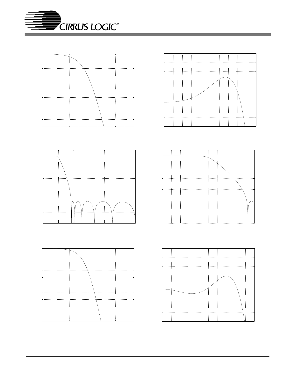
5
5
1
6
5
5
CS4272
0
1
2
3
4
5
Amplitude (dB)
6
7
8
9
10
0.45 0.46 0.47 0.48 0.49 0.5 0.51 0.52 0.53 0.54 0.5
Frequency(normalized to Fs)
0.02
0.015
0.01
0.005
0
Amplitude (dB)
0.005
0.01
0.015
0.02
0 0.05 0.1 0.15 0.2 0.25 0.3 0.35 0.4 0.45 0.
Frequency(normalized to Fs)
Figure 27. DAC Single Speed (slow) Transition Band (detail) Figure 28. DAC Single Speed (slow) Passband Ripple
0
20
40
60
Amplitude (dB)
80
0
20
40
60
Amplitude (dB)
80
100
120
0.4 0.5 0.6 0.7 0.8 0.9
Frequency(normalized to Fs)
100
120
0.4 0.42 0.44 0.46 0.48 0.5 0.52 0.54 0.56 0.58 0.
Frequency(normalized to Fs)
Figure 29. DAC Double Speed (fast) Stopband Rejection Figure 30. DAC Double Speed (fast) Transition Band
0
1
2
3
4
5
Amplitude (dB)
6
7
8
9
10
0.45 0.46 0.47 0.48 0.49 0.5 0.51 0.52 0.53 0.54 0.5
Frequency(normalized to Fs)
0.02
0.015
0.01
0.005
0
Amplitude (dB)
0.005
0.01
0.015
0.02
0 0.05 0.1 0.15 0.2 0.25 0.3 0.35 0.4 0.45 0.
Frequency(normalized to Fs)
Figure 31. DAC Double Speed (fast) Transition Band (detail) Figure 32. DAC Double Speed (fast) Passband Ripple
48 DS593F1
Page 49

1
8
5
5
1
8
CS4272
0
20
40
60
Amplitude (dB)
80
100
120
0.2 0.3 0.4 0.5 0.6 0.7 0.8 0.9
Frequency(normalized to Fs)
0
20
40
60
Amplitude (dB)
80
100
120
0.2 0.3 0.4 0.5 0.6 0.7 0.
Frequency(normalized to Fs)
Figure 33. DAC Double Speed (slow) Stopband Rejection Figure 34. DAC Double Speed (slow) Transition Band
0
1
2
3
4
5
Amplitude (dB)
6
7
8
9
10
0.45 0.46 0.47 0.48 0.49 0.5 0.51 0.52 0.53 0.54 0.5
Frequency(normalized to Fs)
0.02
0.015
0.01
0.005
0
Amplitude (dB)
0.005
0.01
0.015
0.02
0 0.05 0.1 0.15 0.2 0.25 0.3 0.3
Frequency(normalized to Fs)
Figure 35. DAC Double Speed (slow) Transition Band (detail) Figure 36. DAC Double Speed (slow) Passband Ripple
0
20
40
60
Amplitude (dB)
80
100
120
0.2 0.3 0.4 0.5 0.6 0.7 0.8 0.9
Frequency(normalized to Fs)
0
20
40
60
Amplitude (dB)
80
100
120
0.2 0.3 0.4 0.5 0.6 0.7 0.
Frequency(normalized to Fs)
Figure 37. DAC Quad Speed (fast) Stopband Rejection Figure 38. DAC Quad Speed (fast) Transition Band
DS593F1 49
Page 50
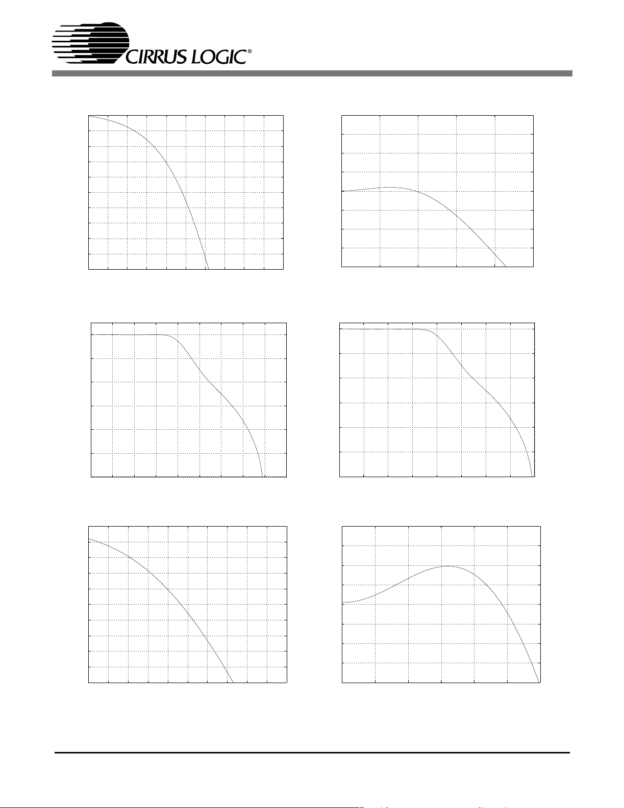
5
5
1
9
5
2
CS4272
0
1
2
3
4
5
Amplitude (dB)
6
7
8
9
10
0.45 0.46 0.47 0.48 0.49 0.5 0.51 0.52 0.53 0.54 0.5
Frequency(normalized to Fs)
0.2
0.15
0.1
0.05
0
Amplitude (dB)
0.05
0.1
0.15
0.2
0 0.05 0.1 0.15 0.2 0.2
Frequency(normalized to Fs)
Figure 39. DAC Quad Speed (fast) Transition Band (detail) Figure 40. DAC Quad Speed (fast) Passband Ripple
0
20
40
60
Amplitude (dB)
80
0
20
40
60
Amplitude (dB)
80
100
120
0.1 0.2 0.3 0.4 0.5 0.6 0.7 0.8 0.9
Frequency(normalized to Fs)
100
120
0.1 0.2 0.3 0.4 0.5 0.6 0.7 0.8 0.
Frequency(normalized to Fs)
Figure 41. DAC Quad Speed (slow) Stopband Rejection Figure 42. DAC Quad Speed (slow) Transition Band
0
1
2
3
4
5
Amplitude (dB)
6
7
8
9
10
0.45 0.46 0.47 0.48 0.49 0.5 0.51 0.52 0.53 0.54 0.5
Frequency(normalized to Fs)
0.02
0.015
0.01
0.005
0
Amplitude (dB)
0.005
0.01
0.015
0.02
0 0.02 0.04 0.06 0.08 0.1 0.1
Frequency(normalized to Fs)
Figure 43. DAC Quad Speed (slow) Transition Band (detail) Figure 44. DAC Quad Speed (slow) Passband Ripple
50 DS593F1
Page 51

0
-10
-20
-30
-40
-50
-60
-70
-80
Amplitude (dB)
-90
-100
-110
-120
-130
-140
0.0 0.1 0.2 0.3 0.4 0.5 0.6 0.7 0.8 0.9 1.0
Frequency (normalized to Fs)
Figure 45. ADC Single Speed Mode Stopband Rejection Figure 46. ADC Single Speed Mode Transition Band
0
-10
-20
-30
-40
-50
-60
-70
-80
Amplitude (dB)
-90
-100
-110
-120
-130
-140
0.40 0.42 0.44 0.46 0.48 0.50 0.52 0.54 0.56 0.58 0.60
Frequency (normalized to Fs)
CS4272
0
-1
-2
-3
-4
-5
Amplitude (dB)
-6
-7
-8
-9
-10
0.45 0.46 0.47 0.48 0.49 0.50 0.51 0.52 0.53 0.54 0.55
Frequency (normalized to Fs)
0.10
0.08
0.05
0.03
0.00
Amplitude (dB)
-0.03
-0.05
-0.08
-0.10
0.00 0.05 0.10 0.15 0.20 0.25 0.30 0.35 0.40 0.45 0.50
Frequency (normalized to Fs)
Figure 47. ADC Single Speed Mode Transition Band (Detail) Figure 48. ADC Single Speed Mode Passband Ripple
0
-10
-20
-30
-40
-50
-60
-70
-80
Amplitude (dB)
-90
-100
-110
-120
-130
-140
0.00.10.20.30.40.50.60.70.80.91.0
Frequency (normalized to Fs)
0
-10
-20
-30
-40
-50
-60
-70
-80
Amplitude (dB)
-90
-100
-110
-120
-130
-140
0.40 0.43 0.45 0.48 0.50 0.53 0.55 0.58 0.60 0.63 0.65 0.68 0.70
Frequency (normalized to Fs)
Figure 49. ADC Double Speed Mode Stopband Rejection Figure 50. ADC Double Speed Mode Transition Band
DS593F1 51
Page 52

CS4272
0
-1
-2
-3
-4
-5
Amplitude (dB)
-6
-7
-8
-9
-10
0.40 0.43 0.45 0.48 0.50 0.53 0.55
Frequency (normalized to Fs)
0.10
0.08
0.05
0.03
0.00
Amplitude (dB)
-0.03
-0.05
-0.08
-0.10
0.00 0.05 0.10 0.15 0.20 0.25 0.30 0.35 0.40 0.45 0.50
Frequency (normalized to Fs)
Figure 51. ADC Double Speed Mode Transition Band (Detail) Figure 52. ADC Double Speed Mode Passband Ripple
0
-10
-20
-30
-40
-50
-60
-70
Amplitude (dB)
-80
-90
-100
-110
-120
0.00.10.20.30.40.50.60.70.80.91.0
Frequency (normalized to Fs)
0
-10
-20
-30
-40
-50
-60
-70
Amplitude (dB)
-80
-90
-100
-110
-120
-130
0.2 0.25 0.3 0.35 0.4 0.45 0.5 0.55 0.6 0.65 0.7 0.75 0.8
Frequency (normalized to Fs)
Figure 53. ADC Quad Speed Mode Stopband Rejection Figure 54. ADC Quad Speed Mode Transition Band
0
-1
-2
-3
-4
-5
Amplitude (dB)
-6
-7
-8
-9
-10
0.1 0.15 0.2 0.25 0.3 0.35 0.4 0.45 0.5 0.55 0.6
Frequency (normalized to Fs)
0.10
0.08
0.06
0.04
0.02
0.00
Amplitude (dB)
-0.02
-0.04
-0.06
-0.08
-0.10
0.00 0.05 0.10 0.15 0.20 0.25
Frequency (normalized to Fs)
Figure 55. ADC Quad Speed Mode Transition Band (Detail) Figure 56. ADC Quad Speed Mode Passband Ripple
52 DS593F1
Page 53

Table 18. Revision History
Release Date Changes
A1 January 2003 Advance Release
PP1 March 2003 Preliminary Release
PP2 October 2003 - Updated Figure 8 on page 23.
- Updated Table 9 on page 29.
- Updated the DC Electrical Characteristics table on page 17.
- Updated the DAC Analog Filter Response tables on pages 10 and 11.
- Updated the ADC Digital Filter Characteristics table on page 16.
- Updated the DAC Full Scale Differential Output Voltage specification on
pages 10 and 11.
PP3 September 2004 Add lead-free device ordering info.
F1 August 2005 Final Release
- Updated Ordering Information on page 2.
- Updated Specified Ope rating Co nditions table on page 9 to reflect orderingsuffix independent temperature grade information.
- Updated DAC Analog Characteristics tables on pages 10 and 11 to reflect
ordering-suffix independent temperature grade information.
- Updated ADC Analog Characteristics tables on pages 14 and 15 to reflect
ordering-suffix independent temperature grade information.
- Updated the DC Electrical Characteristics table on page 17.
- Corrected error in the SCLK Period units shown in the Switching Characteristics - Serial Audio Port table on page 18.
- Corrected error in the Memory Address Pointer table on page 36.
- Updated Chip ID register description on page 44.
CS4272
Contacting Cirrus Logic Support
For all product questions and inquiries contact a Cirrus Logic Sales Representative.
To find one nearest you go to www.cirrus.com
IIMPORTANT NOTICE
Cirrus Logic, Inc. and its subsidiaries ("Cirrus") believe that the information contained in this document is accurate and reliable. However, the information is sub -
ject to change without notice an d is prov ided "AS IS " withou t warra nty of any k ind (exp ress or i mplied ). Customer s are advi sed to obtain the latest version of
relevant information to verify, before plac ing orde rs, that inform ation be ing relie d on is curren t and com plete. All p rodu cts are sold subject to the terms and conditions of sale supplied at the time of order acknowledgment, including those pertaining to warr anty, indemnification, and limitation of liability. No responsibility
is assumed by Cirrus for t he use of t his inf ormatio n, inclu ding use of this i nformati on as the b asis for man ufactu re or sale of any i tems, or for inf ringe ment of
patents or other rights of third parties. This document is the prop erty of Cirrus a nd by fur nishing t his in formatio n, Cir rus grants no license, express or implied
under any patents, mask wo r k ri gh t s, cop y ri ght s, t r adema rk s, t r ade s e cre t s or ot h er in tel l ec t ua l pr o per ty r ig ht s . Ci r r us owns t he copyrights associated with the
information containe d her ei n an d gi ve s c ons ent f or c opi es to b e made o f th e i n for mat i on on l y for u se wi t hi n yo ur or gan iz at i on w it h r esp ect t o Ci rrus i nt egra t ed
circuits or other products of Cirrus. T his consen t does not extend to oth er copyin g such a s copying for ge neral d istribution, a dver tising or promo tional p urpos es,
or for creating any work for resale.
CERTAIN APPLICATIONS USING SEMICONDUCTOR PRODUCTS MAY INVOLVE POTENTIAL RISKS OF DEATH, PERSONAL INJURY, OR SEVERE
PROPERTY OR ENVIRONMENTAL DAMAGE ("CRITICAL APPLICATIONS"). CIRRUS PRODUCTS ARE NOT DESIGNED, AUTHORIZED OR WARRANTED
FOR USE IN AIRCRAFT SYSTEMS, MILITARY APPLICATIONS, PRODUCTS SURGICALLY IMPLANTED INTO THE BODY, AUTOMOTIVE SAFETY OR SECURITY DEVICES, LIFE SUPPORT PRODUCTS OR OTHER CRITICAL APPLICATIONS. INCLUSION OF CIRRUS PRODUCTS IN SUCH APPLICATIONS
IS UNDERSTOOD TO BE FULLY AT THE CUSTOMER'S RISK AND CIRRUS DISCLAIMS AND MAKES NO WARRANTY, EXPRESS, STATUTORY OR IMPLIED, INCLUDING THE IMPLIED WARRANTIES OF MERCHANTABILITY AND FITNESS FOR PARTICULAR PURPOSE, WITH REGARD TO ANY CIRRUS
PRODUCT THAT IS USED IN SUCH A MANNER. IF THE CUSTOMER OR CUSTOMER'S CUSTOMER USES OR PERMITS THE USE OF CIRRUS PRODUCTS IN CRITICAL APPLICATIONS, CUSTOMER AGREES, BY SUCH USE, TO FULLY INDEMNIFY CIRRUS, ITS OFFICERS, DIRECTORS, EMPLOYEES,
DISTRIBUTORS AND OTHER AGENTS FROM ANY AND ALL LIABI LITY, INCL UDING ATTORNEY S' FEES AND COSTS, THAT MAY RESULT FR OM OR
ARISE IN CONNECTION WITH THESE USES.
Cirrus Logic, Cirrus , and th e Cir r us Log ic l ogo d esi gn s ar e t ra de marks o f Cir r us Lo gi c , Inc. All other brand and pr o du ct na mes in thi s doc ume nt may be t r ademarks or service marks of their respective owners.
SPI is a trademark of Motorola, Inc.
DS593F1 53
 Loading...