

Page 1
RST
RXP0
RXP1/GPO1
AD0/CS
SCL/CCLK
SDA/CDOUT
AD1/CDIN
VLC
AOUTA1+
AOUTA1-
AOUTB1+
AOUTA3+
AOUTA3-
AOUTA2-
AOUTB2-
AOUTA2+
AOUTB2+
AOUTB1-
AOUTB3+
AOUTB3-
AOUTA4+
AOUTA4-
AOUTB4+
AOUTB4-
AINL+
AINL-
AINR+
AINR-
FILT+
REFGND
VQ
Ref
ADC#1
ADC#2
Digital Filter
Digital Filter
Gain & Clip
Gain & Clip
CX_SDOUT
ADCIN1
ADCIN2
CX_SCLK
CX_LRCK
CX_SDIN4
CX_SDIN3
CX_SDIN2
CX_SDIN1
VLS
SAI_LRCK
SAI_SCLK
SAI_SDOUT
DGND VD
OMCK
RMCK
LPFLTTXP
INT
Rx
Clock/Data
Recovery
S/PDIF
Decoder
DEM
Serial
Audio
Interface
Port
C&U Bit
Data Buffer
Control
Port
DAC#1
DAC#2
DAC#3
DAC#4
DAC#5
DAC#6
DAC#7
DAC#8
Digital Filter
Volume Control
DGND
RXP2/GPO2
RXP3/GPO3
RXP4/GPO4
RXP5/GPO5
RXP6/GPO6
RXP7/GPO7
VD
MUTEC
GPO
Analog Filter
VARX AGND
ADC
Serial
Data
AGND
VA
Internal MCLK
CODEC
Serial
Port
Mult/Div
Format
Detector
MUTE
CS42528
114 dB, 192-kHz 8-Ch CODEC with S/PDIF Receiver
Features
Eight 24-bit D/A, two 24-bit A/D Converters
114 dB DAC / 114 dB ADC Dynamic Range
-100 dB THD+N
System Sampling Rates up to 192 kHz
S/PDIF Receiver Compatible with EIAJ
CP1201 and IEC-60958
Recovered S/PDIF Clock or System Clock
Selection
8:2 S/PDIF Input MUX
ADC High-Pass Filter for DC Offset Calibration
Expandable ADC Channels and One-Line
Mode Support
Digital Output Volume Control with Soft Ramp
Digital ±15 dB Input Gain Adjust for ADC
Differential Analog Architecture
Supports Logic Levels between 1.8 V and 5 V
General Description
The CS42528 provides two analog-to-digital and eight
digital-to-analog delta-sigma converters, as well as an
integrated S/PDIF receiver.
The CS42528 integrated S/PDIF receiver supports up
to eight inputs, clock recovery circuitry and format autodetection. The internal stereo ADC is capable of independent channel gain control for single-ended or
differential analog inputs. All eight channels of DAC provide digital volume control and differential analog
outputs. The general-purpose outputs may be driven
high or low, or mapped to a variety of DAC mute controls or ADC overflow indicators.
The CS42528 is ideal for audio systems requiring wide
dynamic range, negligible distortion and low noise, such
as A/V receivers, DVD receivers, and digital speakers.
The CS42528 is available in a 64-pin LQFP package in
Commercial (-10° to +70° C) grades. The CDB42528
Customer Demonstration board is also available for device evaluation. Refer to “Ordering Information” on
page 90.
Copyright Cirrus Logic, Inc. 2014
(All Rights Reserved)
MAR '14
DS586F2
http://www.cirrus.com
Page 2

TABLE OF CONTENTS
1. CHARACTERISTICS AND SPECIFICATIONS ...................................................................................... 6
SPECIFIED OPERATING CONDITIONS ............................................................................................... 6
ABSOLUTE MAXIMUM RATINGS ......................................................................................................... 6
ANALOG INPUT CHARACTERISTICS .................................................................................................. 7
A/D DIGITAL FILTER CHARACTERISTICS .......................................................................................... 8
ANALOG OUTPUT CHARACTERISTICS .............................................................................................. 9
D/A DIGITAL FILTER CHARACTERISTICS ........................................................................................ 10
SWITCHING CHARACTERISTICS ......................................................................................................11
SWITCHING CHARACTERISTICS - CONTROL PORT - I²C™ FORMAT ........................................... 12
SWITCHING CHARACTERISTICS - CONTROL PORT - SPI
DC ELECTRICAL CHARACTERISTICS .............................................................................................. 14
DIGITAL INTERFACE CHARACTERISTICS ....................................................................................... 15
2. PIN DESCRIPTIONS ............................................................................................................................ 16
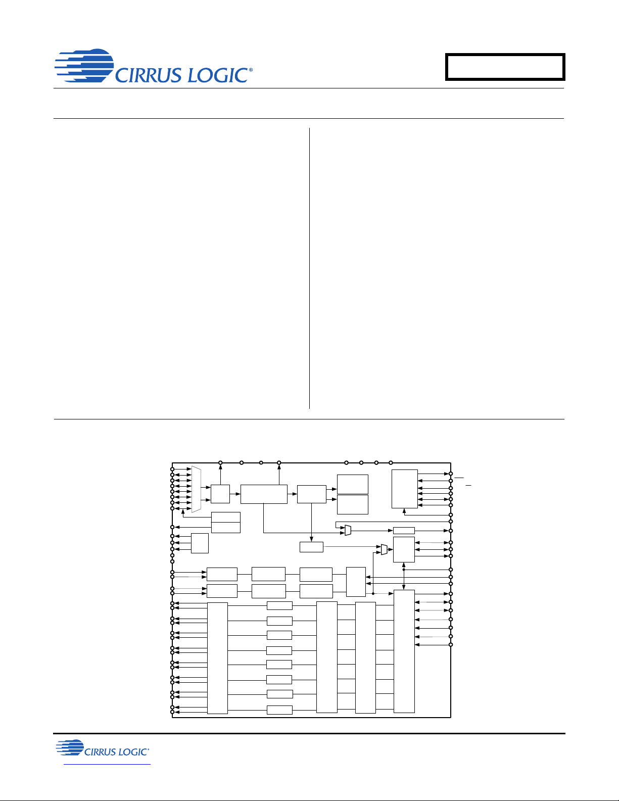
3. TYPICAL CONNECTION DIAGRAM ............................................................................................... 19
4. APPLICATIONS ................................................................................................................................... 20
4.1 Overview ......................................................................................................................................... 20
4.2 Analog Inputs .................................................................................................................................. 20
4.2.1 Line-Level Inputs ................................................................................................................... 20
4.2.2 High-Pass Filter and DC Offset Calibration ........................................................................... 21
4.3 Analog Outputs ............................................................................................................................... 21
4.3.1 Line-Level Outputs and Filtering ........................................................................................... 21
4.3.2 Interpolation Filter .................................................................................................................. 21
4.3.3 Digital Volume and Mute Control ........................................................................................... 22
4.3.4 ATAPI Specification ............................................................................................................... 22
4.4 S/PDIF Receiver ............................................................................................................................. 23
4.4.1 8:2 S/PDIF Input Multiplexer ................................................................................................. 23
4.4.2 Error Reporting and Hold Function ........................................................................................23
4.4.3 Channel Status Data Handling .............................................................................................. 23
4.4.4 User Data Handling ............................................................................................................... 23
4.4.5 Non-Audio Auto-Detection ..................................................................................................... 23
4.5 Clock Generation ............................................................................................................................ 24
4.5.1 PLL and Jitter Attenuation ..................................................................................................... 24
4.5.2 OMCK System Clock Mode ...................................................................................................25
4.5.3 Master Mode ......................................................................................................................... 25
4.5.4 Slave Mode ........................................................................................................................... 25
4.6 Digital Interfaces ............................................................................................................................. 26
4.6.1 Serial Audio Interface Signals ............................................................................................... 26
4.6.2 Serial Audio Interface Formats .............................................................................................. 28
4.6.3 ADCIN1/ADCIN2 Serial Data Format .................................................................................... 31
4.6.4 One-Line Mode (OLM) Configurations .................................................................................. 32
4.6.4.1 OLM Config #1 ........................................................................................................... 32
4.6.4.2 OLM Config #2 ........................................................................................................... 33
4.6.4.3 OLM Config #3 ........................................................................................................... 34
4.6.4.4 OLM Config #4 ........................................................................................................... 35
4.6.4.5 OLM Config #5 ........................................................................................................... 36
4.7 Control Port Description and Timing ............................................................................................... 37
4.7.1 SPI Mode ............................................................................................................................... 37
4.7.2 I²C Mode ................................................................................................................................ 38
4.8 Interrupts ........................................................................................................................................ 39
4.9 Reset and Power-Up ...................................................................................................................... 39
4.10 Power Supply, Grounding, and PCB Layout ................................................................................ 39
5. REGISTER QUICK REFERENCE ........................................................................................................ 41
CS42528
™
FORMAT .......................................... 13
2 DS586F2
Page 3

CS42528
6. REGISTER DESCRIPTION .................................................................................................................. 45
6.1 Memory Address Pointer (MAP) ..................................................................................................... 45
6.2 Chip I.D. and Revision Register (address 01h) (Read Only) .......................................................... 45
6.3 Power Control (address 02h) .......................................................................................................... 46
6.4 Functional Mode (address 03h) ...................................................................................................... 47
6.5 Interface Formats (address 04h) .................................................................................................... 49
6.6 Misc Control (address 05h) ............................................................................................................ 50
6.7 Clock Control (address 06h) ........................................................................................................... 52
6.8 OMCK/PLL_CLK Ratio (address 07h) (Read Only) ....................................................................... 53
6.9 RVCR Status (address 08h) (Read Only) ....................................................................................... 54
6.10 Burst Preamble PC and PD Bytes (addresses 09h - 0Ch)(Read Only) ........................................ 55
6.11 Volume Transition Control (address 0Dh) .................................................................................... 56
6.12 Channel Mute (address 0Eh) ........................................................................................................ 58
6.13 Volume Control (addresses 0Fh, 10h, 11h, 12h, 13h, 14h, 15h, 16h) ...................................... 58
6.14 Channel Invert (address 17h) ....................................................................................................... 58
6.15 Mixing Control Pair 1 (Channels A1 & B1) (address 18h)
Mixing Control Pair 2 (Channels A2 & B2) (address 19h)
Mixing Control Pair 3 (Channels A3 & B3) (address 1Ah)
Mixing Control Pair 4 (Channels A4 & B4) (address 1Bh) ........................................................... 58
6.16 ADC Left Channel Gain (address 1Ch) ........................................................................................ 61
6.17 ADC Right Channel Gain (address 1Dh) ......................................................................................61
6.18 Receiver Mode Control (address 1Eh) ......................................................................................... 61
6.19 Receiver Mode Control 2 (address 1Fh) ...................................................................................... 63
6.20 Interrupt Status (address 20h) (Read Only) ................................................................................. 63
6.21 Interrupt Mask (address 21h) ....................................................................................................... 64
6.22 Interrupt Mode MSB (address 22h)
Interrupt Mode LSB (address 23h) ...............................................................................................65
6.23 Channel Status Data Buffer Control (address 24h) ...................................................................... 65
6.24 Receiver Channel Status (address 25h) (Read Only) .................................................................. 66
6.25 Receiver Errors (address 26h) (Read Only) .................................................................................67
6.26 Receiver Errors Mask (address 27h) ............................................................................................ 68
6.27 Mutec Pin Control (address 28h) .................................................................................................. 69
6.28 RXP/General-Purpose Pin Control (addresses 29h to 2Fh) ......................................................... 69
6.29 Q-Channel Subcode Bytes 0 to 9 (addresses 30h to 39h) (Read Only) ....................................... 71
6.30 C-Bit or U-Bit Data Buffer (addresses 3Ah to 51h) (Read Only) .................................................. 71
7. PARAMETER DEFINITIONS ................................................................................................................ 72
8. APPENDIX A: EXTERNAL FILTERS ................................................................................................... 73
8.1 ADC Input Filter .............................................................................................................................. 73
8.2 DAC Output Filter ........................................................................................................................... 73
9. APPENDIX B: S/PDIF RECEIVER ....................................................................................................... 74
9.1 Error Reporting and Hold Function ................................................................................................. 74
9.2 Channel Status Data Handling ....................................................................................................... 74
9.2.1 Channel Status Data E Buffer Access ................................................................................... 75
9.2.1.1 One-Byte Mode ..........................................................................................................75
9.2.1.2 Two-Byte Mode ..........................................................................................................75
9.2.2 Serial Copy Management System (SCMS) ........................................................................... 76
9.3 User (U) Data E Buffer Access ....................................................................................................... 76
9.3.1 Non-Audio Auto-Detection ..................................................................................................... 76
9.3.1.1 Format Detection .......................................................................................................76
10. APPENDIX C: PLL FILTER ................................................................................................................ 77
10.1 External Filter Components .......................................................................................................... 77
10.1.1 General ................................................................................................................................ 77
10.1.2 Jitter Attenuation ................................................................................................................. 79
10.1.3 Capacitor Selection ............................................................................................................. 80
DS586F2 3
Page 4

10.1.4 Circuit Board Layout ............................................................................................................ 81
11. APPENDIX D: EXTERNAL AES3-S/PDIF-IEC60958 RECEIVER COMPONENTS .......................... 82
11.1 AES3 Receiver External Components .......................................................................................... 82
12. APPENDIX E: ADC FILTER PLOTS .................................................................................................. 83
13. APPENDIX F: DAC FILTER PLOTS .................................................................................................. 85
14. PACKAGE DIMENSIONS ............................................................................................................... 89
THERMAL CHARACTERISTICS .......................................................................................................... 89
15. ORDERING INFORMATION .............................................................................................................. 90
16. REFERENCES .................................................................................................................................... 90
17. REVISION HISTORY ......................................................................................................................... 91
LIST OF FIGURES
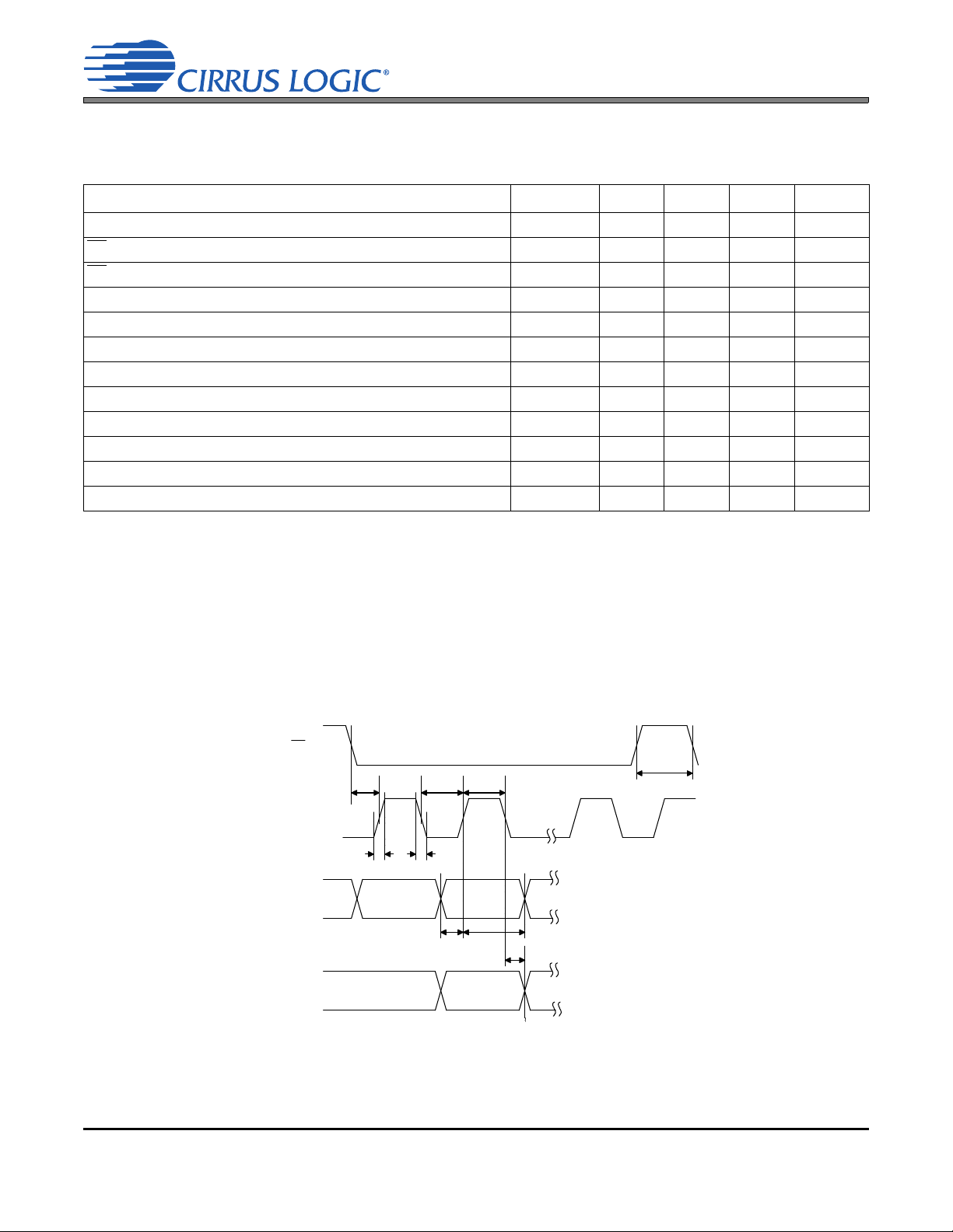
Figure 1. Serial Audio Port Master Mode Timing ...................................................................................... 11
Figure 2. Serial Audio Port Slave Mode Timing ........................................................................................ 11
Figure 3. Control Port Timing - I²C Format ................................................................................................ 12
Figure 4. Control Port Timing - SPI Format ............................................................................................... 13
Figure 5. Typical Connection Diagram ...................................................................................................... 19
Figure 6. Full-Scale Analog Input .............................................................................................................. 20
Figure 7. Full-Scale Output ....................................................................................................................... 21
Figure 8. ATAPI Block Diagram (x = channel pair 1, 2, 3, 4) ....................................................................22
Figure 9. CS42528 Clock Generation ....................................................................................................... 24
Figure 10. I²S Serial Audio Formats .......................................................................................................... 28
Figure 11. Left-Justified Serial Audio Formats .......................................................................................... 29
Figure 12. Right-Justified Serial Audio Formats ........................................................................................ 29
Figure 13. One-Line Mode #1 Serial Audio Format .................................................................................. 30
Figure 14. One-Line Mode #2 Serial Audio Format .................................................................................. 30
Figure 15. ADCIN1/ADCIN2 Serial Audio Format ..................................................................................... 31
Figure 16. OLM Configuration #1 .............................................................................................................. 32
Figure 17. OLM Configuration #2 .............................................................................................................. 33
Figure 18. OLM Configuration #3 .............................................................................................................. 34
Figure 19. OLM Configuration #4 .............................................................................................................. 35
Figure 20. OLM Configuration #5 .............................................................................................................. 36
Figure 21. Control Port Timing in SPI Mode ............................................................................................. 37
Figure 22. Control Port Timing, I²C Write .................................................................................................. 38
Figure 23. Control Port Timing, I²C Read .................................................................................................. 38
Figure 24. Recommended Analog Input Buffer ......................................................................................... 73
Figure 25. Recommended Analog Output Buffer ...................................................................................... 73
Figure 26. Channel Status Data Buffer Structure ...................................................................................... 75
Figure 27. PLL Block Diagram .................................................................................................................. 77
Figure 28. Jitter-Attenuation Characteristics of PLL - Configurations 1 & 2 .............................................. 79
Figure 29. Jitter-Attenuation Characteristics of PLL - Configuration 3 ...................................................... 79
Figure 30. Recommended Layout Example .............................................................................................. 81
Figure 31. Consumer Input Circuit ............................................................................................................ 82
Figure 32. S/PDIF MUX Input Circuit ........................................................................................................ 82
Figure 33. TTL/CMOS Input Circuit ........................................................................................................... 82
Figure 34. Single-Speed Mode Stopband Rejection ................................................................................. 83
Figure 35. Single-Speed Mode Transition Band ....................................................................................... 83
Figure 36. Single-Speed Mode Transition Band (Detail) ........................................................................... 83
Figure 37. Single-Speed Mode Passband Ripple ..................................................................................... 83
Figure 38. Double-Speed Mode Stopband Rejection ................................................................................83
Figure 39. Double-Speed Mode Transition Band ...................................................................................... 83
Figure 40. Double-Speed Mode Transition Band (Detail) ......................................................................... 84
Figure 41. Double-Speed Mode Passband Ripple .................................................................................... 84
CS42528
4 DS586F2
Page 5

CS42528
Figure 42. Quad-Speed Mode Stopband Rejection ..................................................................................84
Figure 43. Quad-Speed Mode Transition Band ........................................................................................ 84
Figure 44. Quad-Speed Mode Transition Band (Detail) ............................................................................84
Figure 45. Quad-Speed Mode Passband Ripple ...................................................................................... 84
Figure 46. Single-Speed (fast) Stopband Rejection .................................................................................. 85
Figure 47. Single-Speed (fast) Transition Band ........................................................................................ 85
Figure 48. Single-Speed (fast) Transition Band (detail) ............................................................................ 85
Figure 49. Single-Speed (fast) Passband Ripple ...................................................................................... 85
Figure 50. Single-Speed (slow) Stopband Rejection ................................................................................ 85
Figure 51. Single-Speed (slow) Transition Band ....................................................................................... 85
Figure 52. Single-Speed (slow) Transition Band (detail) ........................................................................... 86
Figure 53. Single-Speed (slow) Passband Ripple ..................................................................................... 86
Figure 54. Double-Speed (fast) Stopband Rejection ................................................................................ 86
Figure 55. Double-Speed (fast) Transition Band ....................................................................................... 86
Figure 56. Double-Speed (fast) Transition Band (detail) ........................................................................... 86
Figure 57. Double-Speed (fast) Passband Ripple ..................................................................................... 86
Figure 58. Double-Speed (slow) Stopband Rejection ............................................................................... 87
Figure 59. Double-Speed (slow) Transition Band ..................................................................................... 87
Figure 60. Double-Speed (slow) Transition Band (detail) ......................................................................... 87
Figure 61. Double-Speed (slow) Passband Ripple ................................................................................... 87
Figure 62. Quad-Speed (fast) Stopband Rejection ................................................................................... 87
Figure 63. Quad-Speed (fast) Transition Band ......................................................................................... 87
Figure 64. Quad-Speed (fast) Transition Band (detail) ............................................................................. 88
Figure 65. Quad-Speed (fast) Passband Ripple ....................................................................................... 88
Figure 66. Quad-Speed (slow) Stopband Rejection .................................................................................. 88
Figure 67. Quad-Speed (slow) Transition Band ........................................................................................ 88
Figure 68. Quad-Speed (slow) Transition Band (detail) ............................................................................ 88
Figure 69. Quad-Speed (slow) Passband Ripple ...................................................................................... 88
LIST OF TABLES
Table 1. Common OMCK Clock Frequencies ............................................................................................ 25
Table 2. Common PLL Output Clock Frequencies..................................................................................... 25
Table 3. Slave Mode Clock Ratios ............................................................................................................. 26
Table 4. Serial Audio Port Channel Allocations ......................................................................................... 27
Table 5. DAC De-Emphasis ....................................................................................................................... 48
Table 6. Receiver De-Emphasis ................................................................................................................ 48
Table 7. Digital Interface Formats .............................................................................................................. 49
Table 8. ADC One-Line Mode.................................................................................................................... 49
Table 9. DAC One-Line Mode.................................................................................................................... 49
Table 10. RMCK Divider Settings .............................................................................................................. 52
Table 11. OMCK Frequency Settings ........................................................................................................ 52
Table 12. Master Clock Source Select....................................................................................................... 53
Table 13. AES Format Detection ............................................................................................................... 54
Table 14. Receiver Clock Frequency Detection......................................................................................... 55
Table 15. Example Digital Volume Settings ............................................................................................... 58
Table 16. ATAPI Decode ........................................................................................................................... 60
Table 17. Example ADC Input Gain Settings ............................................................................................. 61
Table 18. TXP Output Selection................................................................................................................. 63
Table 19. Receiver Input Selection ............................................................................................................ 63
Table 20. Auxiliary Data Width Selection ................................................................................................... 66
Table 21. External PLL Component Values & Locking Modes .................................................................. 77
DS586F2 5
Page 6
CS42528
1. CHARACTERISTICS AND SPECIFICATIONS
(All Min/Max characteristics and specifications are guaranteed over the Specified Operating Conditions. Typical
performance characteristics and specifications are derived from measurements taken at nominal supply voltages
and T
= 25° C.)
A
SPECIFIED OPERATING CONDITIONS
(AGND=DGND=0, all voltages with respect to ground; OMCK=12.288 MHz; Master Mode)
Parameter Symbol Min Typ Max Units
DC Power Supply Analog
Digital
Serial Port Interface
Control Port Interface
Ambient Operating Temperature (power applied)
VA / VARX
VD
VLS
VLC
T
A
4.75
3.13
1.8
1.8
-10 - +70 C
5.0
3.3
5.0
5.0
5.25
5.25
5.25
5.25
V
V
V
V
ABSOLUTE MAXIMUM RATINGS
(AGND = DGND = 0 V; all voltages with respect to ground.)
Parameters Symbol Min Max Units
DC Power Supply Analog
Digital
Serial Port Interface
Control Port Interface
Input Current (Note 1)
Analog Input Voltage (Note 2)
Digital Input Voltage Serial Port Interface
(Note 2) Control Port Interface
S/PDIF interface
Ambient Operating Temperature(power applied)
Storage Temperature
WARNING: Operation at or beyond these limits may result in permanent damage to the device. Normal operation
is not guaranteed at these extremes.
VA / VA R X
VD
VLS
VLC
I
in
V
IN
V
IND-S
V
IND-C
V
IND-SP
T
A
T
A
T
stg
-0.3
-0.3
-0.3
-0.3
-±10mA
6.0
6.0
6.0
6.0
V
V
V
V
AGND-0.7 VA+0.7 V
-0.3
-0.3
-0.3
-20
-50
-65 +150 °C
VLS+ 0.4
VLC+ 0.4
VAR X+0.4
+85
+95
V
V
V
°C
°C
Notes:
1. Any pin except supplies. Transient currents of up to ±100 mA on the analog input pins will not cause
SCR latch-up.
2. The maximum over/under voltage is limited by the input current.
6 DS586F2
Page 7
CS42528
ANALOG INPUT CHARACTERISTICS
(TA = 25° C; VA =VARX= 5 V, VD = 3.3 V, Logic “0” = DGND =AGND = 0 V; Logic “1” = VLS = VLC = 5 V; Measurement Bandwidth is 10 Hz to 20 kHz unless otherwise specified. Full-scale input sine wave, 997 Hz.;
PDN_RCVR = 1; SW_CTRL[1:0] = ‘01’; OMCK = 12.288 MHz; Single-Speed Mode CX_SCLK = 3.072 MHz; Double-Speed Mode CX_SCLK = 6.144 MHz; Quad-Speed Mode CX_SCLK = 12.288 MHz.)
Parameter Symbol Min Typ Max Unit
Single-Speed Mode (Fs=48 kHz)
Dynamic Range A-weighted
unweighted
Total Harmonic Distortion + Noise
(Note 3) -1 dB
-20 dB
-60 dB
Double-Speed Mode (Fs=96 kHz)
Dynamic Range A-weighted
unweighted
40 kHz bandwidth unweighted
Total Harmonic Distortion + Noise
(Note 3) -1 dB
-20 dB
-60 dB
40 kHz bandwidth -1 dB
Quad-Speed Mode (Fs=192 kHz)
Dynamic Range A-weighted
unweighted
40 kHz bandwidth unweighted
Total Harmonic Distortion+ Noise
(Note 3) -1 dB
-20 dB
-60 dB
40 kHz bandwidth -1 dB
Dynamic Performance for All Modes
Interchannel Isolation
Interchannel Phase Deviation
DC Accuracy
Interchannel Gain Mismatch
Gain Drift
Offset Error HPF_FREEZE disabled
HPF_FREEZE enabled
Analog Input
Full-scale Differential Input Voltage
Input Impedance (Differential) (Note 4)
Common Mode Rejection Ratio
THD+N
THD+N
THD+N
CMRR - 82 - dB
108
105
-
-
-
108
105
-
-
-
-
-
108
105
-
-
-
-
-
-110- dB
- 0.0001 - Degree
-0.1-dB
- +/-100 - ppm/°C
-
-
1.05 VA 1.10 VA 1.16 VA Vpp
17 - - k
114
111
-100
-91
-51
114
111
108
-100
-91
-51
-97
114
111
108
-100
-91
-51
-97
0
100
-94
-94
-94
-
-
-
-
-
-
-
-
-
-
-
-
-
-
-
-
-
-
dB
dB
dB
dB
dB
dB
dB
dB
dB
dB
dB
dB
dB
dB
dB
dB
dB
dB
dB
LSB
LSB
Notes:
3. Referred to the typical full-scale voltage.
4. Measured between AIN+ and AIN-
DS586F2 7
Page 8
A/D DIGITAL FILTER CHARACTERISTICS
Parameter Symbol Min Typ Max Unit
Single-Speed Mode (2 to 50 kHz sample rates)
Passband (-0.1 dB) (Note 5)
Passband Ripple
Stopband (Note 5)
Stopband Attenuation
Total Group Delay (Fs = Output Sample Rate)
Group Delay Variation vs. Frequency
Double-Speed Mode (50 to 100 kHz sample rates)
Passband (-0.1 dB) (Note 5)
Passband Ripple
Stopband (Note 5)
Stopband Attenuation
Total Group Delay (Fs = Output Sample Rate)
Group Delay Variation vs. Frequency
Quad-Speed Mode (100 to 192 kHz sample rates)
Passband (-0.1 dB) (Note 5)
Passband Ripple
Stopband (Note 5)
Stopband Attenuation
Total Group Delay (Fs = Output Sample Rate)
Group Delay Variation vs. Frequency
High-Pass Filter Characteristics
Frequency Response -3.0 dB
-0.13 dB (Note 6)
Phase Deviation @ 20 Hz (Note 6)
Passband Ripple
Filter Setting Time
t
t
t
CS42528
0 - 0.47 Fs
--0.035 dB
0.58 - - Fs
-95 - - dB
t
gd
gd
t
gd
gd
t
gd
gd
-12/Fs- s
--0.0s
0 - 0.45 Fs
--0.035 dB
0.68 - - Fs
-92 - - dB
-9/Fs- s
--0.0s
0 - 0.24 Fs
--0.035 dB
0.78 - - Fs
-97 - - dB
-5/Fs- s
--0.0s
-120-
-
-10-Deg
--0dB
-10
5
/Fs - s
Hz
Hz
Notes:
5. The filter frequency response scales precisely with Fs.
6. Response shown is for Fs equal to 48 kHz. Filter characteristics scale with Fs.
8 DS586F2
Page 9
CS42528
ANALOG OUTPUT CHARACTERISTICS
(TA = 25° C; VA =VARX= 5 V, VD = 3.3 V, Logic “0” = DGND =AGND = 0 V; Logic “1” = VLS = VLC = 5V; Measure-
dB
dB
dB
dB
dB
dB
dB
dB
dB
dB
=
L
ment Bandwidth 10 Hz to 20 kHz unless otherwise specified.; Full-scale output 997 Hz sine wave, Test load R
3k, C
= 30 pF; PDN_RCVR = 1; SW_CTRL[1:0] = ‘01’; OMCK = 12.288 MHz; Single-Speed Mode, CX_SCLK =
L
3.072 MHz; Double-Speed Mode, CX_SCLK = 6.144 MHz; Quad-Speed Mode, CX_SCLK = 12.288 MHz.)
Parameter Symbol Min Typ Max Unit
Dynamic performance for all modes
Dynamic Range (Note 7)
24-bit A-Weighted
unweighted
16-bit A-Weighted
(Note 8) unweighted
Total Harmonic Distortion + Noise
24-bit 0 dB
-20 dB
-60 dB
16-bit 0 dB
(Note 8) -20 dB
-60 dB
Idle Channel Noise/Signal-to-Noise Ratio (A-Weighted)
Interchannel Isolation (1 kHz)
THD+N
108
105
-
-
-
-
-
-
-
-
-114 - dB
-90 -dB
114
111
97
94
-100
-91
-51
-94
-74
-34
-
-
-
-
-94
-
-
-
-
Analog Output Characteristics for all modes
Unloaded Full-Scale Differential Output Voltage
Interchannel Gain Mismatch
Gain Drift
Output Impedance
AC-Load Resistance
Load Capacitance
Z
V
OUT
R
C
.89 VA .94 VA .99 VA Vpp
FS
-0.1 - dB
- 300 - ppm/°C
- 150 -
L
L
3- -k
- - 30 pF
Notes:
7. One LSB of triangular PDF dither is added to data.
8. Performance limited by 16-bit quantization noise.
DS586F2 9
Page 10
D/A DIGITAL FILTER CHARACTERISTICS
Fast Roll-Off Slow Roll-Off
Parameter
Combined Digital and On-chip Analog Filter Response - Single-Speed Mode - 48 kHz
Passband (Note 9) to -0.01 dB corner
to -3 dB corner
Frequency Response 10 Hz to 20 kHz
StopBand
StopBand Attenuation (Note 10)
Group Delay
Passband Group Delay Deviation 0 - 20 kHz
De-emphasis Error (Note 11) Fs = 32 kHz
(Relative to 1 kHz) Fs = 44.1 kHz
Fs = 48 kHz
Combined Digital and On-chip Analog Filter Response - Double-Speed Mode - 96 kHz
Passband (Note 9) to -0.01 dB corner
to -3 dB corner
Frequency Response 10 Hz to 20 kHz
StopBand
StopBand Attenuation (Note 10)
Group Delay
Passband Group Delay Deviation 0 - 20 kHz
Combined Digital and On-chip Analog Filter Response - Quad-Speed Mode - 192 kHz
Passband (Note 9) to -0.01 dB corner
to -3 dB corner
Frequency Response 10 Hz to 20 kHz
StopBand
StopBand Attenuation (Note 10)
Group Delay
Passband Group Delay Deviation 0 - 20 kHz
0
0
-0.01 - +0.01 -0.01 - +0.01 dB
0.5465 - - 0.5834 - - Fs
90 - - 64 - - dB
- 12/Fs - - 6.5/Fs - s
- - ±0.41/Fs - ±0.14/Fs s
-
-
-
0
0
-0.01 - 0.01 -0.01 - 0.01 dB
0.5834 - - 0.7917 - - Fs
80 - - 70 - - dB
- 4.6/Fs - - 3.9/Fs - s
- - ±0.03/Fs - ±0.01/Fs s
0
0
-0.01 - 0.01 -0.01 - 0.01 dB
0.6355 - - 0.8683 - - Fs
90 - - 75 - - dB
- 4.7/Fs - - 4.2/Fs - s
- - ±0.01/Fs - ±0.01/Fs s
-
-
-
-
-
-
-
-
-
0.4535
0.4998
±0.23
±0.14
±0.09
0.4166
0.4998
0.1046
0.4897
0
0
-
-
-
0
0
0
0
CS42528
UnitMin Typ Max Min Typ Max
-
-
-
-
-
-
-
-
-
0.4166
0.4998FsFs
±0.23
±0.14
±0.09
0.2083
0.4998FsFs
0.1042
0.4813FsFs
dB
dB
dB
Notes:
9. Response is clock dependent and will scale with Fs. Note that the response plots (Figures 46 to 69) have
been normalized to Fs and can be de-normalized by multiplying the X-axis scale by Fs.
10. Single- and Double-Speed Mode Measurement Bandwidth is from stopband to 3 Fs.
Quad-Speed Mode Measurement Bandwidth is from stopband to 1.34 Fs.
11. De-emphasis is available only in Single-Speed Mode.
10 DS586F2
Page 11
CS42528
CX_SCLK
SAI_SCLK
(output)
RMCK
t
smd
t
lmd
CX_LRCK
SAI_LRCK
(output)
sckh
sckl
t
t
MSB
MSB-1
t
dpd
CX_SDOUT
SAI_SDOUT
CX_SDINx
dh
t
ds
t
lrpd
t
lrck
t
CX_SCLK
SAI_SCLK
(input)
CX_LRCK
SAI_LRCK
(input)
Figure 1. Serial Audio Port Master Mode Timing Figure 2. Serial Audio Port Slave Mode Timing
SWITCHING CHARACTERISTICS
(TA = -10 to +70° C; VA=VARX = 5 V, VD =VLC= 3.3 V, VLS = 1.8 V to 5.25 V; Inputs: Logic 0 = DGND, Logic 1 =
VLS, C
RST Pin Low Pulse Width (Note 12)
PLL Clock Recovery Sample Rate Range
RMCK Output Jitter (Note 14)
RMCK Output Duty Cycle (Note 15)
OMCK Frequency (Note 13)
OMCK Duty Cycle (Note 13)
CX_SCLK, SAI_SCLK Duty Cycle
CX_LRCK, SAI_LRCK Duty Cycle
Master Mode
RMCK to CX_SCLK, SAI_SCLK active edge delay
RMCK to CX_LRCK, SAI_LRCK delay
Slave Mode
CX_SCLK, SAI_SCLK Falling Edge to CX_SDOUT,
SAI_SDOUT Output Valid
CX_LRCK, SAI_LRCK Edge to MSB Valid
CX_SDIN Setup Time Before CX_SCLK Rising Edge
CX_SDIN Hold Time After CX_SCLK Rising Edge
CX_SCLK, SAI_SCLK High Time
CX_SCLK, SAI_SCLK Low Time
CX_SCLK, SAI_SCLK falling to CX_LRCK, SAI_LRCK
Edge
= 30 pF)
L
Parameters Symbol Min Typ Max Units
1--ms
30 - 200 kHz
- 200 - ps RMS
45 50 55 %
1.024 - 25.600 MHz
40 50 60 %
45 50 55 %
45 50 55 %
t
smd
t
lmd
t
dpd
t
lrpd
t
ds
t
dh
t
sckh
t
sckl
t
lrck
0-15ns
0-15ns
- (Note 16) ns
-26.5ns
10 - - ns
30 - - ns
20 - - ns
20 - - ns
-25 - +25 ns
Notes:
12. After powering-up the CS42528, RST
should be held low after the power supplies and clocks are set-
tled.
13. See Table 1 on page 25 for suggested OMCK frequencies
14. Limit the loading on RMCK to 1 CMOS load if operating above 24.576 MHz.
15. Not valid when RMCK_DIV in “Clock Control (address 06h)” on page 52 is set to Multiply by 2.
16. 76.5 ns for Single-Speed and Double-Speed modes, 23 ns for Quad-Speed Mode.
DS586F2 11
Page 12
CS42528
15
256 Fs
---------------------
15
128 Fs
---------------------
15
64 Fs
------------------
t
buf
t
hdst
t
low
t
hdd
t
high
t
sud
Stop Start
SDA
SCL
t
irs
RST
t
hdst
t
rc
t
fc
t
sust
t
susp
Start
Stop
Repeated
t
rd
t
fd
t
ack
Figure 3. Control Port Timing - I²C Format
SWITCHING CHARACTERISTICS - CONTROL PORT - I²C™ FORMAT
(TA = -10 to +70° C; VA=VARX = 5 V, VD =VLS= 3.3 V; VLC = 1.8 V to 5.25 V; Inputs: Logic 0 = DGND, Logic
1=VLC, C
SCL Clock Frequency
Rising Edge to Start
RST
Bus Free Time Between Transmissions
Start Condition Hold Time (prior to first clock pulse)
Clock Low time
Clock High Time
Setup Time for Repeated Start Condition
SDA Hold Time from SCL Falling (Note 17)
SDA Setup time to SCL Rising
Rise Time of SCL and SDA
Fall Time SCL and SDA
Setup Time for Stop Condition
Acknowledge Delay from SCL Falling (Note 18)
=30pF)
L
Parameter Symbol Min Max Unit
f
scl
t
t
buf
t
hdst
t
low
t
high
t
sust
t
hdd
t
sud
t
t
t
susp
t
ack
irs
rc
fc
- 100 kHz
500 - ns
4.7 - µs
4.0 - µs
4.7 - µs
4.0 - µs
4.7 - µs
0-µs
250 - ns
-1µs
- 300 ns
4.7 - µs
- (Note 19) ns
Notes:
17. Data must be held for sufficient time to bridge the transition time, t
, of SCL.
fc
18. The acknowledge delay is based on MCLK and can limit the maximum transaction speed.
19. for Single-Speed Mode, for Double-Speed Mode, for Quad-Speed Mode
12 DS586F2
Page 13
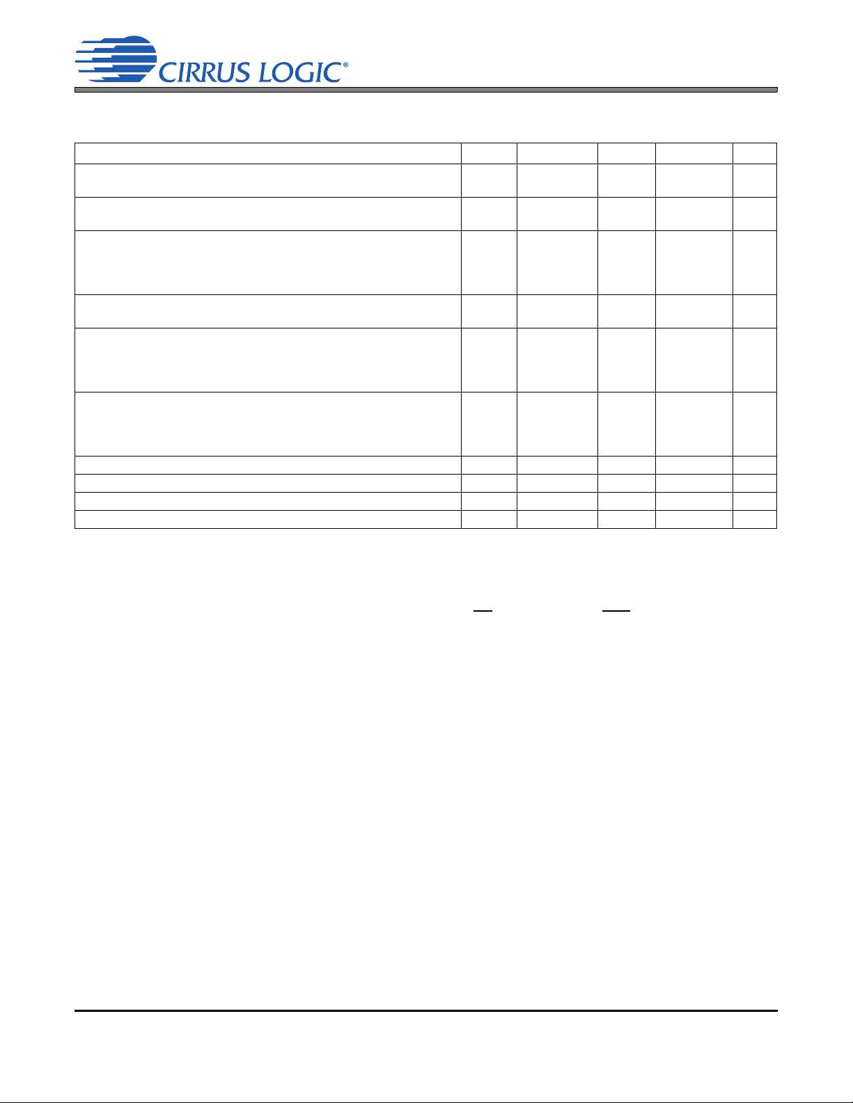
CS42528
t
r2
t
f2
t
dsu
t
dh
t
sch
t
scl
CS
CCLK
CDIN
t
css
t
pd
CDOUT
t
csh
Figure 4. Control Port Timing - SPI Format
SWITCHING CHARACTERISTICS - CONTROL PORT - SPI™ FORMAT
(TA = -10 to +70° C; VA=VARX = 5 V, VD =VLS= 3.3 V; VLC = 1.8 V to 5.25 V; Inputs: Logic 0 = DGND, Logic
1=VLC, C
CCLK Clock Frequency (Note 20)
High Time Between Transmissions
CS
Falling to CCLK Edge
CS
CCLK Low Time
CCLK High Time
CDIN to CCLK Rising Setup Time
CCLK Rising to DATA Hold Time (Note 21)
CCLK Falling to CDOUT Stable
Rise Time of CDOUT
Fall Time of CDOUT
Rise Time of CCLK and CDIN (Note 22)
Fall Time of CCLK and CDIN (Note 22)
Notes:
=30pF)
L
Parameter Symbol Min Typ Max Units
f
t
t
t
t
t
t
t
sck
csh
css
scl
sch
dsu
dh
pd
t
r1
t
f1
t
r2
t
f2
0-6.0MHz
1.0 - - s
20 - - ns
66 - - ns
66 - - ns
40 - - ns
15 - - ns
--50ns
--25ns
--25ns
--100ns
--100ns
20. If Fs is lower than 46.875 kHz, the maximum CCLK frequency should be less than 128 Fs. This is
dictated by the timing requirements necessary to access the Channel Status and User Bit buffer
memory. Access to the control register file can be carried out at the full 6 MHz rate. The minimum
allowable input sample rate is 8 kHz, so choosing CCLK to be less than or equal to 1.024 MHz should
be safe for all possible conditions.
21. Data must be held for sufficient time to bridge the transition time of CCLK.
22. For f
<1 MHz.
sck
DS586F2 13
Page 14
DC ELECTRICAL CHARACTERISTICS
(TA = 25° C; AGND=DGND=0, all voltages with respect to ground; OMCK=12.288 MHz; Master Mode)
Parameter Symbol Min Typ Max Units
Power Supply Current normal operation, VA = VARX = 5 V
(Note 23) VD = 5 V
VD = 3.3 V
Interface current, VLC=5 V (Note 24)
VLS=5 V
power-down state (all supplies) (Note 25)
Power Consumption (Note 23)
VA=VARX=5 V, VD=VLS=VLC=3.3 V normal operation
power-down (Note 25)
VA=VARX=5 V, VD=VLS=VLC=5 V normal operation
power-down (Note 25)
Power Supply Rejection Ratio (Note 26) (1 kHz)
(60 Hz)
VQ Nominal Voltage
VQ Output Impedance
VQ Maximum allowable DC current
FILT+ Nominal Voltage
FILT+ Output Impedance
FILT+ Maximum allowable DC current
I
A
I
D
I
D
I
LC
I
LS
I
pd
PSRR
-
-
-
-
-
-
-
-
-
-
-
-
-
-
-
-
-
-
75
85
51
250
13
250
587
1.25
866
1.25
60
40
2.7
50
0.01
5.0
35
0.01
-
-
-
-
-
-
650
-
960
-
-
-
-
-
-
-
-
-
CS42528
mA
mA
mA
A
mA
A
mW
mW
mW
mW
dB
dB
V
k
mA
V
k
mA
Notes:
23. Current consumption increases with increasing FS and increasing OMCK. Max values are based on
highest FS and highest OMCK. Variance between speed modes is negligible.
24. I
25. Power-Down Mode is defined as RST
measured with no external loading on the SDA pin.
LC
pin = Low with all clock and data lines held static.
26. Valid with the recommended capacitor values on FILT+ and VQ as shown in Figure 5.
14 DS586F2
Page 15
DIGITAL INTERFACE CHARACTERISTICS
(TA = +25° C)
Parameters (Note 27) Symbol Min Typ Max Units
High-Level Input Voltage Serial Port
Control Port
Low-Level Input Voltage Serial Port
Control Port
High-Level Output Voltage at I
Low-Level Output Voltage at I
Serial Port, Control Port, MUTEC, GPOx,TXP
High-Level Output Voltage at I
Low-Level Output Voltage at I
Input Sensitivity, RXP[7:0]
Input Leakage Current
Input Capacitance
MUTEC Drive Current
=2 mA (Note 28)Serial Port
o
Control Port
MUTEC, GPOx
TXP
=2 mA (Note 28)
o
=100 A (Note 28)Serial Port
o
Control Port
MUTEC, GPOx
TXP
=100 A (Note 28)Serial Port
o
Control Port
MUTEC, GPOx
TXP
CS42528
V
IH
V
IL
V
OH
V
OL
V
OH
V
OL
V
TH
I
in
0.7xVLS
0.7xVLC
-
-
VLS-1.0
VLC-1.0
VA- 1.0
VD-1.0
-
-
-
-
-
-
-
-
-
-
0.2xVLS
0.2xVLC
-
-
-
-
V
V
V
V
V
V
V
V
--0.4V
0.8xVLS
0.8xVLC
0.8xVA
0.8xVD
-
-
-
-
-
-
-
-
-
-
-
-
-
-
-
-
0.2xVLS
0.2xVLC
0.2xVA
0.2xVD
V
V
V
V
V
V
V
V
- 150 200 mVpp
--±10A
-8-pF
-3-mA
Notes:
27. Serial Port signals include: RMCK, OMCK, SAI_SCLK, SAI_LRCK, SAI_SDOUT, CX_SCLK, CX_LRCK, CX_SDOUT, CX_SDIN1-4, ADCI N 1/2 Con t rol
Port signals include: SCL/CCLK, SDA/CDOUT, AD0/CS
, AD1/CDIN, INT, RST S/PDIF-
GPO Interface signals include: RXP0, RXP/GPO[1:7]
28. When operating RMCK above 24.576 MHz, limit the loading on the signal to 1 CMOS load.
DS586F2 15
Page 16
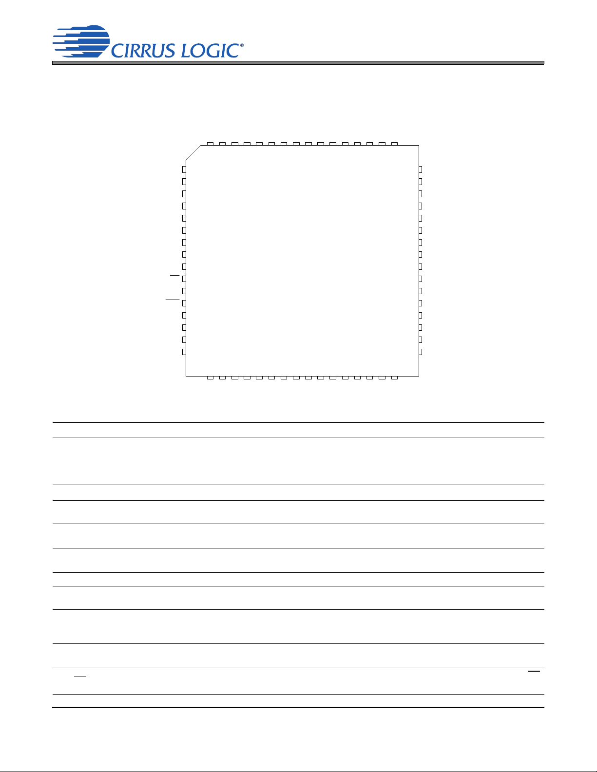
2. PIN DESCRIPTIONS
1
2
3
4
5
6
7
8
9
10
11
12
13
14
15
16
17 18 19 20 21 22 23 24 25 26 27 28 29 30 31 32
64 63 62 61 60 59 58 57 56 55 54 53 52 51 50 49
48
47
46
45
44
43
42
41
40
39
38
37
36
35
34
33
CX_SDIN1
SAI_SCLK
SAI_LRCK
VD
DGND
VLC
SCL/CCLK
SDA/CDOUT
AD1/CDIN
AD0/CS
INT
RST
AINR-
AINR+
AINL+
AINL-
VQ
FILT+
REFGND
AOUTB4-
AOUTB4+
AOUTA4+
AOUTA4-
VA
AGND
AOUTB3-
AOUTB3+
AOUTA3+
AOUTA3-
AOUTB2-
AOUTB2+
AOUTA2+
AOUTA2-
AOUTB1-
AOUTB1+
AOUTA1+
AOUTA1-
MUTEC
AGND
VARX
RXP7/GPO7
RXP6/GPO6
RXP5/GPO5
RXP4/GPO4
RXP3/GPO3
RXP2/GPO2
RXP1/GPO1
LPFLT
RXP0
TXP
VD
DGND
VLS
SAI_SDOUT
RMCK
CX_SDOUT
ADCIN2
ADCIN1
OMCK
CX_LRCK
CX_SCLK
CX_SDIN4
CX_SDIN3
CX_SDIN2
CS42526
CS42528
Pin Name # Pin Description
CX_SDIN1
CX_SDIN2
CX_SDIN3
CX_SDIN4
CX_SCLK
CX_LRCK
VD
DGND
VLC
SCL/CCLK
SDA/CDOUT
AD1/CDIN
AD0/CS
16 DS586F2
1
64
Codec Serial Audio Data Input (Input) - Input for two’s complement serial audio data.
63
62
2
3
CODEC Serial Clock (Input/Output) - Serial clock for the CODEC serial audio interface.
CODEC Left Right Clock (Input/Output) - Determines which channel, Left or Right, is currently active on
the CODEC serial audio data line.
4
Digital Power (Input) - Positive power supply for the digital section.
51
5
Digital Ground (Input) - Ground reference. Should be connected to digital ground.
52
6
Control Port Power (Input) - Determines the required signal level for the control port.
Serial Control Port Clock (Input) - Serial clock for the serial control port. Requires an external pull-up
7
resistor to the logic interface voltage in I²C mode as shown in the Typical Connection Diagram.
Serial Control Data (Input/Output) - SDA is a data I/O line in I²C mode and requires an external pull-up
8
resistor to the logic interface voltage, as shown in the Typical Connection Diagram. CDOUT is the output
data line for the control port interface in SPI mode.
Address Bit 1 (I²C)/Serial Control Data (SPI) (Input) - AD1 is a chip address pin in I²C mode; CDIN is
9
the input data line for the control port interface in SPI mode.
Address Bit 0 (I²C)/Control Port Chip Select (SPI) (Input) - AD0 is a chip address pin in I²C mode; CS
10
is the chip select signal in SPI mode.
Page 17
INT
RST
AINRAINR+
AINL+
AINL-
VQ
FILT+
REFGND
AOUTA1 +,AOUTB1 +,AOUTA2 +,AOUTB2 +,AOUTA3 +,AOUTB3 +,AOUTA4 +,AOUTB4 +,-
VA
VAR X
AGND
MUTEC
LPFLT
RXP7/GPO7
RXP6/GPO6
RXP5/GPO5
RXP4/GPO4
RXP3/GPO3
RXP2/GPO2
RXP1/GPO1
RXP0
TXP
VLS
SAI_SDOUT
RMCK
CX_SDOUT
ADCIN1
ADCIN2
Interrupt (Output) - The CS42528 will generate an interrupt condition as per the Interrupt Mask register.
11
See “Interrupts” on page 39 for more details.
Reset (Input) - The device enters a low power mode and all internal registers are reset to their default
12
settings when low.
13
Differential Right Channel Analog Input (Input) - Signals are presented differentially to the delta-sigma
14
modulators via the AINR+/- pins.
15
Differential Left Channel Analog Input (Input) - Signals are presented differentially to the delta-sigma
16
modulators via the AINL+/- pins.
17
Quiescent Voltage (Output) - Filter connection for internal quiescent reference voltage.
18
Positive Voltage Reference (Output) - Positive reference voltage for the internal sampling circuits.
19
Reference Ground (Input) - Ground reference for the internal sampling circuits.
36,37
35,34
32,33
31,30
Differential Analog Output (Output) - The full-scale differential analog output level is specified in the
28,29
Analog Characteristics specification table.
27,26
22,23
21,20
24
Analog Power (Input) - Positive power supply for the analog section.
41
25
Analog Ground (Input) - Ground reference. Should be connected to analog ground.
40
Mute Control (Output) - The Mute Control pin outputs high impedance following an initial power-on con-
dition or whenever the PDN bit is set to a ‘1’, forcing the codec into power-down mode. The signal will
remain in a high impedance state as long as the part is in power-down mode. The Mute Control pin goes
38
to the selected “active” state during reset, muting, or if the master clock to left/right clock frequency ratio
is incorrect. This pin is intended to be used as a control for external mute circuits to prevent the clicks
and pops that can occur in any single supply system. The use of external mute circuits are not manda-
tory but may be desired for designs requiring the absolute minimum in extraneous clicks and pops.
39
PLL Loop Filter (Output) - An RC network should be connected between this pin and ground.
42
S/PDIF Receiver Input/ General Purpose Output (Input/Output) - Receiver inputs for S/PDIF encoded
43
data. The CS42528 has an internal 8:2 multiplexer to select the active receiver port, according to the
44
Receiver Mode Control 2 register. These pins can also be configured as general purpose output pins,
45
ADC Overflow indicators or Mute Control outputs according to the RXP/General Purpose Pin Control
46
registers.
47
48
S/PDIF Receiver Input (Input) - Dedicated receiver input for S/PDIF encoded data.
49
S/PDIF Transmitter Output (Output) - S/PDIF encoded data output, mapped directly from one of the
50
receiver inputs as indicated by the Receiver Mode Control 2 register.
53
Serial Port Interface Power (Input) - Determines the required signal level for the serial port interfaces.
Serial Audio Interface Serial Data Output (Output) - Output for two’s complement serial audio PCM
54
data from the S/PDIF incoming stream. This pin can also be configured to transmit the output of the inter-
nal and external ADCs.
Recovered Master Clock (Output) - Recovered master clock output from the External Clock Reference
55
(OMCK, pin 59) or the PLL which is locked to the incoming S/PDIF stream or CX_LRCK.
CODEC Serial Data Output (Output) - Output for two’s complement serial audio data from the internal
56
and external ADCs.
External ADC Serial Input (Input) - The CS42528 provides for up to two external stereo analog to digital
58
converter inputs to provide a maximum of six channels on one serial data output line when the CS42528
57
is placed in One-Line Mode.
CS42528
DS586F2 17
Page 18

OMCK
SAI_LRCK
SAI_SCLK
CS42528
External Reference Clock (Input) - External clock reference that must be within the ranges specified in
59
the register “OMCK Frequency (OMCK Freqx)” on page 52.
Serial Audio Interface Left/Right Clock (Input/Output) - Determines which channel, Left or Right, is
60
currently active on the serial audio data line.
Serial Audio Interface Serial Clock (Input/Output) - Serial clock for the Serial Audio Interface.
61
18 DS586F2
Page 19
3. TYPICAL CONNECTION DIAGRAM
VD
AOUTA1+
24
0.1 µF
+
10 µF
100 µF
0.1 µF
+
+
17
18
VQ
FILT+
36
37
0.1 µF
4.7 µF
VA
+
10 µF
51
AOUTA1-
AOUTB1+
35
34
AOUTB1-
AOUTA2+
32
33
AOUTA2-
AOUTB2+
31
30
AOUTB2-
AOUTA3+
28
29
AOUTA3-
AOUTB3+
27
26
AOUTB3-
AOUTA4+
22
23
AOUTA4-
AOUTB4+
21
20
AOUTB4-
MUTEC
38
25
DGND
DGND
5
REFGND
19
41
4
VAVD
0.1 µF
AGNDAGND
52 40
LPFLT
39
AINL+
AINL-
AINR+
AINR-
15
16
14
13
Connect DGND and AGN D at single point near Codec
0.01 µF
0.1 µF
+
10 µF
+5 V
0.01 µF
0.01 µF
+3.3 V to + 5 V
+
10 µF
0.1 µF 0.01 µF
VLS
0.1 µF
+2.5 V
to +5 V
53
VLC
0.1 µF
+1.8 V
to +5 V
6
3
60
59
62
1
64
61
2
63
8
7
SCL/CCLK
SDA/CDOUT
AD1/CDIN
RST
12
9
OMCK
CX_SDIN1
SAI_LRCK
SAI_SCLK
CX_SDIN3
CX_SDIN2
CX_SDIN4
CX_LRCK
CX_SCLK
AD0/CS
10
INT
11
Digital A udio
Processor
Micro-
Controller
55
RMCK
58
ADCIN1
57
ADCIN2
CS5361
A/D Converter
CS5361
A/D Converter
56
CX_SDOUT
54
SAI_SDOUT
48
46
49
44
45
47
RXP0
RXP1/GPO1
S/PDIF
Interfac e
50
TXP
Driver
Up to 8
Sources
43
RXP2/GPO2
RXP3/GPO3
RXP4/GPO4
RXP5/GPO5
RXP6/GPO6
RXP7/GPO7
42
OSC
Analog Output Buffer
2
and
Mute Circuit (optional)
Analog Output Buffer
2
and
Mute Circuit (optional)
Analog Output Buffer
2
and
Mute Circuit (optional)
Analog Output Buffer
2
and
Mute Circuit (optional)
Analog Output Buffer
2
and
Mute Circuit (optional)
Analog Output Buffer
2
and
Mute Circuit (optional)
Analog Output Buffer
2
and
Mute Circuit (optional)
Analog Output Buffer
2
and
Mute Circuit (optional)
Mute
Drive
(optional)
+VA
*
* Pull up or down as
required on startup if the
Mute Control is used.
*
2700 pF*
2700 pF*
Left Analog Input
Right Analog Inpu
Analog
Input
Buffer
1
Analog
Input
Buffer
1
CFILT
3
RFILT
3
CRIP
3
2 k 2 k
** **
** Resistors are required for
I
2
C control port operation
1. See the ADC Input Filter section in the Appendix.
2. See the DAC Output Filter section in the Appendix.
3. See the PLL Filter section in the Appendix.
Figure 5. Typical Connection Diagram
CS42526
CS42528
DS586F2 19
Page 20
4. APPLICATIONS
AIN+
AIN-
Full-Scale Input Level= (AIN+) - (AIN-)= 5.6 Vpp
4.1 V
2.7 V
1.3 V
4.1 V
2.7 V
1.3 V
Figure 6. Full-Scale Analog Input
4.1 Overview
The CS42528 is a highly integrated mixed-signal 24-bit audio codec comprised of 2 analog-to-digital converters (ADC), implemented using multi-bit delta-sigma techniques, 8 digital-to-analog converters (DAC)
and a 192 kHz digital audio S/PDIF receiver. Other functions integrated within the codec include independent digital volume controls for each DAC, digital de-emphasis filters for DAC and S/PDIF, digital gain control for ADC channels, ADC high-pass filters, an on-chip voltage reference, and an 8:2 mux for S/PDIF
sources. All serial data is transmitted through two configurable serial audio interfaces with standard serial
interface support as well as enhanced one-line modes of operation, allowing up to 6 channels of serial audio
data on one data line. All functions are configured through a serial control port operable in SPI mode or in
I²C mode. 5 show the recommended connections for the CS42528.
The CS42528 operates in one of three oversampling modes based on the input sample rate. Mode selection
is determined by the FM bits in register “Functional Mode (address 03h)” on page 47. Single-Speed Mode
(SSM) supports input sample rates up to 50 kHz and uses a 128x oversampling ratio. Double-Speed Mode
(DSM) supports input sample rates up to 100 kHz and uses an oversampling ratio of 64x. Quad-Speed
Mode (QSM) supports input sample rates up to 192 kHz and uses an oversampling ratio of 32x.
Using the receiver clock recovery PLL, a low-jitter clock is recovered from the incoming S/PDIF data stream.
The recovered clock or an externally supplied clock attached to the OMCK pin can be used as the System
Clock.
CS42528
4.2 Analog Inputs
4.2.1 Line-Level Inputs
AINR+, AINR-, AINL+, and AINL- are the line-level differential analog inputs. The analog signal must be
externally biased to VQ, approximately 2.7 V, before being applied to these inputs. The level of the signal
can be adjusted for the left and right ADC independently through the ADC Left and Right Channel Gain
Control Registers on page 61. The ADC output data is in two’s complement binary format. For inputs
above positive full scale or below negative full scale, the ADC will output 7FFFFFH or 800000H, respectively and cause the ADC Overflow bit in the register “Interrupt Status (address 20h) (Read Only)” on
page 63 to be set to a ‘1’. The RXP/GPO pins may also be configured to indicate an overflow condition
has occurred in the ADC. See “RXP/General-Purpose Pin Control (addresses 29h to 2Fh)” on page 69
for proper configuration. Figure 6 shows the full-scale analog input levels. See “ADC Input Filter” on
page 73 for a recommended input buffer.
20 DS586F2
Page 21
4.2.2 High-Pass Filter and DC Offset Calibration
AOUT+
AOUT-
Full-Scale Output Level= (AIN+) - (AIN-)= 5 Vpp
3.95 V
2.7 V
1.45 V
3.95 V
2.7 V
1.45 V
Figure 7. Full-Scale Output
The high-pass filter continuously subtracts a measure of the DC offset from the output of the decimation
filter. The high-pass filter can be independently enabled and disabled. If the HPF_Freeze bit is set during
normal operation, the current value of the DC offset for the corresponding channel is frozen and this DC
offset will continue to be subtracted from the conversion result. This feature makes it possible to perform
a system DC offset calibration by:
1. Running the CS42528 with the high-pass filter enabled until the filter settles. See the Digital Filter
Characteristics for filter settling time.
2. Disabling the high-pass filter and freezing the stored DC offset.
The high-pass filters are controlled using the HPF_FREEZE bit in the register “Misc Control (address
05h)” on page 50.
4.3 Analog Outputs
4.3.1 Line-Level Outputs and Filtering
The CS42528 contains on-chip buffer amplifiers capable of producing line-level differential outputs. These
amplifiers are biased to a quiescent DC level of approximately VQ.
The delta-sigma conversion process produces high-frequency noise beyond the audio passband, most of
which is removed by the on-chip analog filters. The remaining out-of-band noise can be attenuated using
an off-chip low-pass filter. See “DAC Output Filter” on page 73 for a recommended output buffer. This filter
configuration accounts for the normally differing AC loads on the AOUT+ and AOUT- differential output
pins. It also shows an AC coupling configuration which minimizes the number of required AC coupling capacitors. Figure 7 shows the full-scale analog output levels.
CS42528
4.3.2 Interpolation Filter
To accommodate the increasingly complex requirements of digital audio systems, the CS42528 incorporates selectable interpolation filters for each mode of operation. A “fast” and a “slow” roll-off filter is avail-
DS586F2 21
able in Single-, Double-, and Quad-Speed Modes. These filters have been designed to accommodate a
variety of musical tastes and styles. The FILT_SEL bit found in the register “Misc Control (address 05h)”
on page 50 selects which filter is used. Filter response plots can be found in Figures 46 to 69.
Page 22
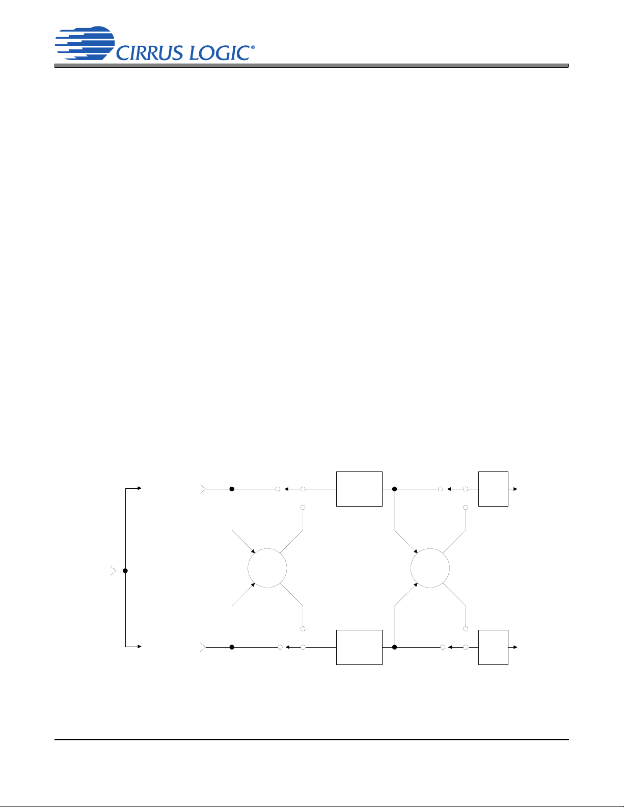
4.3.3 Digital Volume and Mute Control
A Channel
Volume
Control
AOUTAx
AOUTBx
Left Channel
Audio Data
Right Channel
Audio Data
BChannel
Volume
Control
MUTE
MUTE
CX_SDINx
Figure 8. ATAPI Block Diagram (x = channel pair 1, 2, 3, 4)
Each DAC’s output level is controlled via the Volume Control registers operating over the range of 0 to
-127 dB attenuation with 0.5 dB resolution. See “Volume Control (addresses 0Fh, 10h, 11h, 12h, 13h,
14h, 15h, 16h)” on page 58. Volume control changes are programmable to ramp in increments of
0.125 dB at the rate controlled by the SZC[1:0] bits in the Digital Volume Control register. See “Volume
Transition Control (address 0Dh)” on page 56.
Each output can be independently muted via mute control bits in the register “Channel Mute (address
0Eh)” on page 58. When enabled, each XX_MUTE bit attenuates the corresponding DAC to its maximum
value (-127 dB). When the XX_MUTE bit is disabled, the corresponding DAC returns to the attenuation
level set in the Volume Control register. The attenuation is ramped up and down at the rate specified by
the SZC[1:0] bits.
The Mute Control pin, MUTEC, is typically connected to an external mute control circuit. The Mute Control
pin outputs high impedance during Power-Up or in Power-Down Mode by setting the PDN bit in the register “Power Control (address 02h)” on page 46 to a ‘1’. Once out of Power-Down Mode, the pin can be
controlled by the user via the control port, or automatically asserted high when zero data is present on all
DAC inputs, or when serial port clock errors are present. To prevent large transients on the output, it is
desirable to mute the DAC outputs before the Mute Control pin is asserted. Please see the MUTEC pin
in the Pin Descriptions section for more information.
Each of the RXP1/GPO1-RXP7/GPO7 can be programmed to provide a hardware MUTE signal to individual circuits. When not used as an S/PDIF input, each pin can be programmed as an output, with specific muting capabilities as defined by the function bits in the register “RXP/General-Purpose Pin Control
(addresses 29h to 2Fh)” on page 69.
CS42528
4.3.4 ATAPI Specification
The CS42528 implements the channel-mixing functions of the ATAPI CD-ROM specification. The
ATAPI functions are applied per A-B pair. Refer to Table 16 on page 60 and Figure 8 for additional information.
22 DS586F2
Page 23

4.4 S/PDIF Receiver
The CS42528 includes an S/PDIF digital audio receiver. The S/PDIF receiver accepts and decodes digital
audio data according to the IEC60958 (S/PDIF), and EIAJ CP-1201 interface standards. The receiver consists of an 8:2 multiplexer input stage driven through pins RXP0 and RXP1/GPO1 - RXP7/GPO7, a PLL
based clock recovery circuit, and a decoder which separates the audio data from the channel status and
user data. A comprehensive buffering scheme provides read access to the channel status and user data.
External components are used to terminate and isolate the incoming data cables from the CS42528. These
components and required circuitry are detailed in the CDB42528.
4.4.1 8:2 S/PDIF Input Multiplexer
The CS42528 contains an 8:2 S/PDIF Input Multiplexer to accommodate up to eight channels of input digital audio data. Digital audio data is single-ended and input through the RXP0 and
RXP1/GPO1-RXP7/GPO7 pins. Any one of these inputs can be multiplexed to the input of the S/PDIF
receiver and to the S/PDIF output pin TXP.
When any portion of the multiplexer is implemented, unused RXP0 and RXPx/GPOx pins should be tied
to a 0.01uF capacitor to ground. The receiver multiplexer select line control is accessed through bits
RMUX2:0 in the Receiver Mode Control 2 register on page 63. The TXP multiplexer select line control is
accessed through bits TMUX2:0 in the same register. The multiplexer defaults to RXP0 for both functions.
CS42528
4.4.2 Error Reporting and Hold Function
While decoding the incoming S/PDIF data stream, the CS42528 can identify several kinds of error, indicated in the register “Receiver Errors (address 26h) (Read Only)” on page 67. See “Error Reporting and
Hold Function” on page 74 for more information.
4.4.3 Channel Status Data Handling
The first 2 bytes of the Channel Status block (C data) are decoded into the Receiver Channel Status register (See “Receiver Channel Status (address 25h) (Read Only)” on page 66). See “Channel Status Data
Handling” on page 74 for more information.
4.4.4 User Data Handling
The incoming User (U) data is buffered in a user accessible buffer. If the U data bits have been encoded
as Q-channel subcode, the data is decoded and presented in 10 consecutive register locations, address
30h to 39h. The user can configure the Interrupt Mask Register to cause interrupts to indicate the decoding of a new Q-channel block, which may be read through the control port. See “User (U) Data E Buffer
Access” on page 76 for more information.
4.4.5 Non-Audio Auto-Detection
A S/PDIF data stream may be used to convey non-audio data, thus it is important to know whether the
incoming data stream is digital PCM audio samples or not. This information is typically conveyed in channel status bit 1 (AUDIO
however, such as AC-3
properly set. See “Non-Audio Auto-Detection” on page 76 for more information including details for inter-
face format detection.
), which is extracted automatically by the CS42528. Certain non-audio sources,
or MPEG encoders, may not adhere to this convention, and the bit may not be
DS586F2 23
Page 24
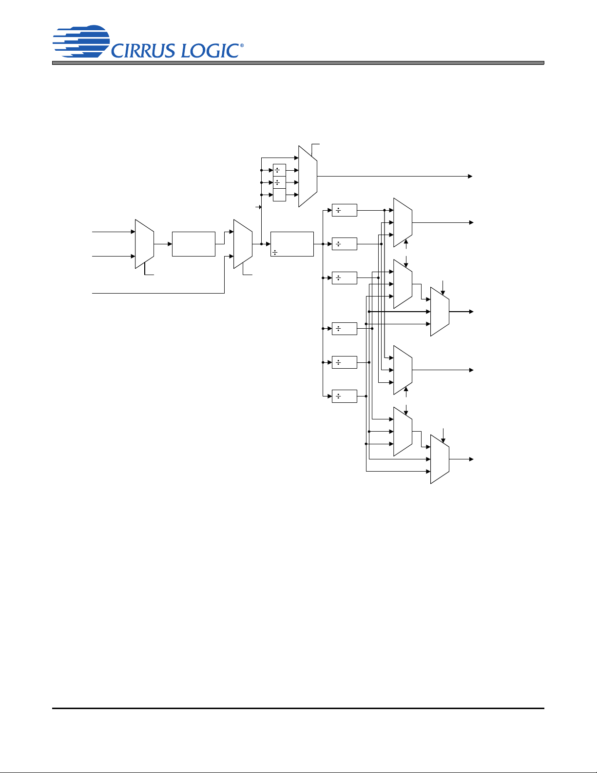
4.5 Clock Generation
SAI_LRCK
(slave mode)
Recovered
S/PDIF Clock
0
1
PLL (256Fs)
8.192 -
49.152 MHz
00
01
PLL_LRCK bit
SW_CTRLx bits
(manual or auto
switch)
OMCK
Auto Detect
Input Clock
1,1.5, 2, 4
single
speed
256
double
speed
128
quad
speed
64
single
speed
4
double
speed
2
quad
speed
1
00
01
10
00
01
10
00
01
10
00
01
10
not OLM
OLM #1
CODEC_FMx bits
SAI_FMx bits
DAC_OLx
or ADC_OLx bits
ADC_OLx and
ADC_SP SELx bits
SAI_SCLK
CX_SCLK
CX_LRCK
SAI_LRCK
RMCK
OLM #2
not OLM
OLM #1
OLM #2
128FS
256FS
128FS
256FS
Internal
MCLK
00
01
10
11
RMCK_DIVx bits
2
4
X2
Figure 9. CS42528 Clock Generation
The clock generation for the CS42528 is shown in the figure below. The internal MCLK is derived from the
output of the PLL or a master clock source attached to OMCK. The mux selection is controlled by the SW_CTRLx bits and can be configured to manual switch mode only, or automatically switch on loss of PLL lock
to the other source input.
CS42528
4.5.1 PLL and Jitter Attenuation
An on-chip Phase Locked Loop (PLL) is used to recover the clock from the incoming S/PDIF data stream.
There are some applications where low jitter in the recovered clock, presented on the RMCK pin, is important. For this reason, the PLL has been designed to have good jitter attenuation characteristics as
shown in Figure 28 on page 79.
The PLL can be configured to lock onto the incoming SAI_LRCK signal from the Serial Audio Interface
Port and generate the required internal master clock frequency. By setting the PLL_LRCK bit to a ‘1’ in
the register “Clock Control (address 06h)” on page 52, the PLL will lock to the incoming SAI_LRCK and
generate an output master clock (RMCK) of 256Fs. Table 2 shows the output of the PLL with typical input
Fs values for SAI_LRCK.
See “Appendix C: PLL Filter” on page 77 for more information concerning PLL operation, required filter
components, optimal layout guidelines, and jitter-attenuation characteristics.
24 DS586F2
Page 25
4.5.2 OMCK System Clock Mode
Sample
Rate
(kHz)
OMCK (MHz)
Single-Speed
(4 to 50 kHz)
Double-Speed
(50 to 100 kHz)
Quad-Speed
(100 to 192 kHz)
256x 384x 512x 128x 192x 256x 64x 96x 128x
48 12.2880 18.4320 24.5760 - - - - - 96 - - - 12.2880 18.4320 24.5760 - - -
192 - - - - - - 12.2880 18.4320 24.5760
Table 1. Common OMCK Clock Frequencies
Sample
Rate
(kHz)
PLL Output (MHz)
Single Speed
(4 to 50 kHz)
Double Speed
(50 to 100 kHz)
Quad Speed
(100 to 192 kHz)
256x 256x 256x
32 8.1920 - -
44.1 11.2896 - 48 12.2880 - 64 - 16.3840 -
88.2 - 22.5792 96 - 24.5760 -
176.4 - - 45.1584
192 - - 49.1520
Table 2. Common PLL Output Clock Frequencies
A special clock-switching mode is available that allows the clock that is input through the OMCK pin to be
used as the internal master clock. This feature is controlled by the SW_CTRLx bits in register “Clock Con-
trol (address 06h)” on page 52. An advanced auto-switching mode is also implemented to maintain mas-
ter clock functionality. The clock auto-switching mode allows the clock input through OMCK to be used as
a clock in the system without any disruption when the PLL loses lock, for example, when the input is removed from the receiver. This clock-switching is done glitch-free. A clock adhering to the specifications
detailed in the Switching Characteristics table on page 11 must be applied to the OMCK pin at all times
that the FRC_PLL_LK bit is set to ‘0’ (See “Force PLL Lock (FRC_PLL_LK)” on page 53).
4.5.3 Master Mode
In Master Mode, the serial interface timings are derived from an external clock attached to OMCK or from
the output of the PLL with an input reference to either the S/PDIF Receiver recovered clock or the SAI_LRCK input from the Serial Audio Interface Port. Master clock selection and operation is configured with
the SW_CTRL1:0 bits in the Clock Control Register (See “Clock Control (address 06h)” on page 52).The
supported PLL output frequencies are shown in Table 2 below.
CS42528
4.5.4 Slave Mode
In Slave Mode, CX_LRCK, CX_SCLK and/or SAI_LRCK, SAI_SCLK operate as inputs. The Left/Right
clock signal must be equal to the sample rate, Fs, and must be synchronously derived from the supplied
DS586F2 25
master clock, OMCK, or the output of the PLL. The serial bit clock, CX_SCLK and/or SAI_SCLK, must be
synchronously derived from the master clock and be equal to 128x, 64x, 48x or 32x Fs, depending on the
interface format selected and desired speed mode.
When the device is clocked from OMCK, the frequency of OMCK must be at least twice the frequency of
the fastest Slave Mode, SCLK. For example, if both serial ports are in Slave Mode with one SCLK running
at 32x Fs and the other at 64x Fs, the slowest OMCK signal that can be used to clock the device is
128x Fs.
Page 26
When either serial port is in Slave Mode, its respective LRCK signal must be present for proper device
operation.
In Slave Mode, One-Line Mode #1 is supported; One-Line Mode #2 is not.
The sample rate to OMCK ratios and OMCK frequency requirements for Slave Mode operation are shown
in Table 1. Refer to Table 3 for required clock ratios.
Single-Speed Double-Speed Quad-Speed One-Line Mode #1
OMCK/LRCK Ratio
SCLK/LRCK Ratio
256x, 384x, 512x 128x, 192x, 256x 64x, 96x, 128x 256x
32x, 48x, 64x, 128x 32x, 48x, 64x 32x, 48x, 64x 128x
Table 3. Slave Mode Clock Ratios
4.6 Digital Interfaces
4.6.1 Serial Audio Interface Signals
The CS42528 interfaces to an external Digital Audio Processor via two independent serial ports, the
CODEC serial port, CODEC_SP and the Serial Audio Interface serial port, SAI_SP. The digital output of
the internal ADCs can be configured to use either the CX_SDOUT pin or the SAI_SDOUT pin and the
corresponding serial port clocking signals. These configuration bits and the selection of Single-, Doubleor Quad-Speed Mode for CODEC_SP and SAI_SP are found in register “Functional Mode (address 03h)”
on page 47.
CS42528
The serial interface clocks, SAI_SCLK for SAI_SP and CX_SCLK for CODEC_SP, are used for transmitting and receiving audio data. Either SAI_SCLK or CX_SCLK can be generated by the CS42528 (Master
Mode), or it can be input from an external source (Slave Mode). Master or Slave Mode selection is made
using bits CODEC_SP M/S
The Left/Right clock (SAI_LRCK or CX_LRCK) is used to indicate left and right data frames and the start
of a new sample period. It may be an output of the CS42528 (Master Mode), or it may be generated by
an external source (Slave Mode). As described in later sections, particular modes of operation do allow
the sample rate, Fs, of the SAI_SP and the CODEC_SP to be different, but must be multiples of each
other.
The serial data interface format selection (Left/Right-Justified, I²S or One-Line Mode) for the Serial Audio
Interface serial port data out pin, SAI_SDOUT, the CODEC serial port data out pin, CX_SDOUT, and the
CODEC input pins, CX_SDIN1:4, is configured using the appropriate bits in the register “Interface For-
mats (address 04h)” on page 49. The serial audio data is presented in two's complement binary form with
the MSB first in all formats.
CX_SDIN1, CX_SDIN2, CX_SDIN3 and CX_SDIN4 are the serial data input pins supplying the associated internal DAC. CX_SDOUT, the ADC data output pin, carries data from the two internal 24-bit ADCs
and, when configured for one-line mode, up to four additional ADC channels attached externally to the
signals ADCIN1 and ADCIN2 (typically two CS5361 stereo ADCs). When operated in One-Line Mode,
6 channels of DAC data are input on CX_SDIN1, two additional DAC channels on CX_SDIN4, and 6 channels of ADC data are output on CX_SDOUT. Table 4 on page 27 outlines the serial port channel allocations.
and SAI_SP M/S in register “Misc Control (address 05h)” on page 50.
26 DS586F2
Page 27
Serial Inputs / Outputs
CX_SDIN1 left channel
right channel
One-Line Mode
CX_SDIN2 left channel
right channel
One-Line Mode
CX_SDIN3 left channel
right channel
One-Line Mode
CX_SDIN4 left channel
right channel
One-Line Mode
CX_SDOUT left channel
right channel
One-Line Mode
SAI_SDOUT left channel
right channel
One-Line Mode
ADCIN1 left channel
right channel
ADCIN2 left channel
right channel
CS42528
DAC #1
DAC #2
DAC channels 1,2,3,4,5,6
DAC #3
DAC #4
not used
DAC #5
DAC #6
not used
DAC #7
DAC #8
DAC channels 7,8
ADC #1
ADC #2
ADC channels 1,2,3,4,5,6
S/PDIF Left or ADC #1
S/PDIF Right or ADC #2
ADC channels 1,2,3,4,5,6
External ADC #3
External ADC #4
External ADC #5
External ADC #6
Table 4. Serial Audio Port Channel Allocations
DS586F2 27
Page 28
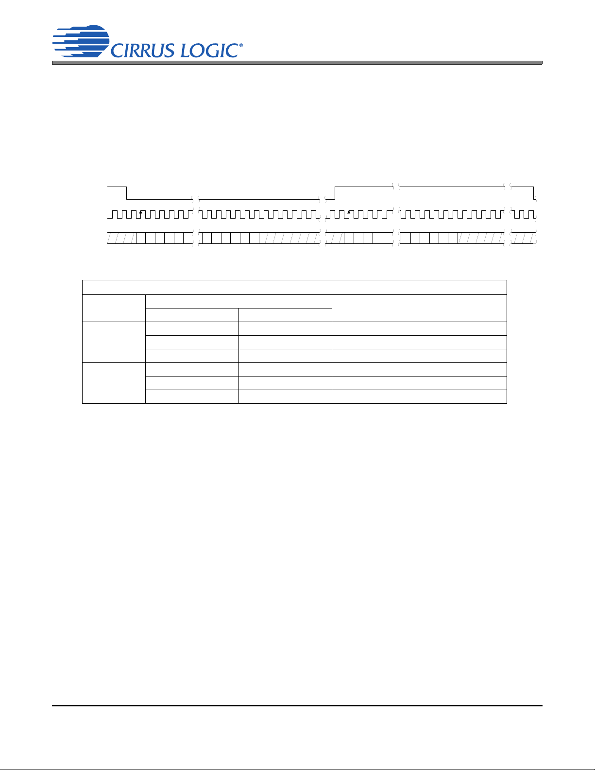
4.6.2 Serial Audio Interface Formats
Left Channel
Right Channel
CX_SDINx
CX_SDOUT
SAI_SDOUT
+3 +2 +1+5 +4
-1 -2 -3 -4 -5
+3 +2 +1+5 +4
-1 -2 -3 -4
MSB
MSB
LSB LSB
CX_LRCK
SAI_LRCK
CX_SCLK
SAI_SCLK
Figure 10. I²S Serial Audio Formats
I²S Mode, Data Valid on Rising Edge of SCLK
Bits/Sample
SCLK Rate(s)
Notes
Master Slave
16
64 48, 64, 128 Fs Single-Speed Mode
64 Fs 64 Fs Double-Speed Mode
64 Fs 64 Fs Quad-Speed Mode
18 to 24
64, 128, 256 Fs 48, 64, 128 Fs Single-Speed Mode
64 Fs 48, 64 Fs Double-Speed Mode
64 Fs 48, 64 Fs Quad-Speed Mode
The CODEC_SP and SAI_SP digital audio serial ports support five formats with varying bit depths from
16 to 24 as shown in Figures 10 to 14. These formats are selected using the configuration bits in the registers, “Functional Mode (address 03h)” on page 47 and “Interface Formats (address 04h)” on page 49.
For the diagrams below, Single-Speed Mode is equivalent to Fs = 32, 44.1, 48 kHz; Double-Speed Mode
is for Fs = 64, 88.2, 96 kHz; and Quad-Speed Mode is for Fs = 176.4, 196 kHz.
CS42528
28 DS586F2
Page 29

CS42528
CX_LRCK
SAI_LRCK
CX_SCLK
SAI_SCLK
Left Channel
Right Channel
CX_SDINx
CX_SDOUT
SAI_SDOUT
+3 +2 +1+5 +4
-1 -2 -3 -4 -5
+3 +2 +1+5 +4
-1
-2 -3 -4
MSB LSB MSB LSB
Figure 11. Left-Justified Serial Audio Formats
Left-Justified Mode, Data Valid on Rising Edge of SCLK
Bits/Sample
SCLK Rate(s)
Notes
Master Slave
16
64 32, 48, 64, 128 Fs Single-Speed Mode
64 Fs 32, 64 Fs Double-Speed Mode
64 Fs 32, 64 Fs Quad-Speed Mode
18 to 24
64, 128, 256 Fs 48, 64, 128 Fs Single-Speed Mode
64 Fs 48, 64 Fs Double-Speed Mode
64 Fs 48, 64 Fs Quad-Speed Mode
Left Channel
Right Channel
6543210987
15 1 4 13 12 11 10
6543210987
15 14 13 12 11 10
CX_SDINx
CX_SDOUT
SAI_SDOUT
CX_LRCK
SAI_LRCK
CX_SCLK
SAI_SCLK
Figure 12. Right-Justified Serial Audio Formats
Right-Justified Mode, Data Valid on Rising Edge of SCLK
Bits/Sample
SCLK Rate(s)
Notes
Master Slave
16
64 32, 48, 64, 128 Fs Single-Speed Mode
64 Fs 32, 64 Fs Double-Speed Mode
64 Fs 32, 64 Fs Quad-Speed Mode
24
64, 128, 256 Fs 48, 64, 128 Fs Single-Speed Mode
64 Fs 48, 64 Fs Double-Speed Mode
64 Fs 48, 64 Fs Quad-Speed Mode
DS586F2 29
Page 30

CS42528
Figure 13. One-Line Mode #1 Serial Audio Format
One-Line Data Mode #1, Data Valid on Rising Edge of SCLK
Bits/Sample
SCLK Rate(s)
Notes
Master Slave
20
128 Fs 128 Fs Single-Speed Mode
128 Fs 128 Fs Double-Speed Mode
CX_LRCK
SAI_LRCK
CX_SCLK
SAI_SCLK
LSBMSB
20 clks
64 clks 64 clks
LSBMSB LSBMSB LSBMSB LSBMSB LSBMSB MSB
DAC1 DAC3 DAC5 DAC2 DAC4 DAC6
20 clks
20 clks 20 clks 20 clks 20 clks
Left Channel Right Channel
20 clks
DAC7 DAC8
20 clks
CX_SDIN4
20 clks
ADC1 ADC3 ADC5 ADC2 A DC4 ADC6
20 clks
20 clks 20 clks 20 clks 20 clks
CX_SDOUT
SAI_SDOUT
CX_SDIN1
LSBMSB
24 clks
128 clks
LSBMSB LSBMS B LSBMSB LSBMSB LSBMS B MS B
DAC1 DAC 3 DAC5 DAC2 DAC4 DAC6
24 clks
24 clks 24 clks 24 clks 24 cl ks
Left Channel Right Channel
24 cl ks
DAC7 DAC8
24 clks
24 cl ks
ADC1 ADC3 ADC5 ADC2 ADC4 ADC6
24 clks
24 cl ks 24 clks 24 clks 24 clks
128 clks
CX_L RCK
SAI_ LRCK
CX_SCL K
SAI_ SCLK
CX_SDOUT
SAI_SDOUT
CX_SDI N1
CX_SDI N4
Figure 14. One-Line Mode #2 Serial Audio Format
One-Line Data Mode #2, Data Valid on Rising Edge of SCLK
Bits/Sample
SCLK Rate(s)
Notes
Master Slave
24 256 Fs Not supported Single-Speed Mode
30 DS586F2
Page 31

4.6.3 ADCIN1/ADCIN2 Serial Data Format
CX_LRCK
SAI_LRCK
CX_SCLK
SAI_SCLK
Left Channel
Right Channel
ADCIN1/2
+3 +2 +1+5 +4
-1 -2 -3 -4 -5
+3 +2 +1+5 +4
-1 -2 -3 -4
MSB LSB MSB LSB
Figure 15. ADCIN1/ADCIN2 Serial Audio Format
Left-Justified Mode, Data Valid on Rising Edge of SCLK
Bits/Sample SCLK Rate(s) Notes
24
64, 128 Fs Single-Speed Mode, Fs= 32, 44.1, 48 kHz
64 Fs Double-Speed Mode, Fs= 64, 88.2, 96 kHz
not supported Quad-Speed Mode, Fs= 176.4, 192 kHz
The two serial data lines which interface to the optional external ADCs, ADCIN1 and ADCIN2, support
only left-justified, 24-bit samples at 64Fs or 128Fs. This interface is not affected by any of the serial port
configuration register bit settings. These serial data lines are used when supporting One-Line Mode of
operation with external ADCs attached. If these signals are not being used, they should be tied together
and wired to GND via a pull-down resistor.
CS42528
For proper operation, the CS42528 must be configured to select which SCLK/LRCK is being used to clock
the external ADCs. The EXT ADC SCLK bit in register “Misc Control (address 05h)” on page 50 must be
set accordingly. Set this bit to ‘1’ if the external ADCs are wired using the CODEC_SP clocks. If the ADCs
are wired to use the SAI_SP clocks, set this bit to ‘0’.
DS586F2 31
Page 32

4.6.4 One-Line Mode (OLM) Configurations
SCLK_PORT1
LRCK_PORT1
SDIN_PORT1
SCLK_PORT2
LRCK_PORT2
SDIN_PORT2
SCLK_PORT3
LRCK_PORT3
SDOUT1_PORT3
SDOUT2_PORT3
SDOUT3_PORT3
SDOUT4_PORT3
SAI_SCLK
SAI_LRCK
SAI_SDOUT
CX_SCLK
CX_LRCK
CX_SDOUT
CX_SDIN1
CX_SDIN2
CX_SDIN3
CX_SDIN4
RMCK
ADCIN1
ADCIN2
MCLK
SDOUT1
SDOUT2
LRCK
SCLK
64Fs
SPDIF Data
ADC Data
64Fs,128Fs, 256Fs
DIGITAL AUDIO
PROCESSOR
CS5361
CS5361
MCLK
Figure 16. OLM Configuration #1
CS42526
4.6.4.1 OLM Config #1
One-Line Mode Configuration #1 can support up to 8 channels of DAC data, 6 channels of ADC data and
2 channels of S/PDIF received data. This is the only configuration which will support up to 24-bit samples
at a sampling frequency of 48 kHz on all channels for both the DAC and ADC.
Register / Bit Settings Description
Functional Mode Register (addr = 03h)
Set CODEC_FMx = SAI_FMx = 00,01,10
Set ADC_SP SELx = 00
Interface Format Register (addr = 04h)
Set DIFx bits to proper serial format
Set ADC_OLx bits = 00,01,10
Set DAC_OLx bits = 00,01,10
Misc. Control Register (addr = 05h)
Set CODEC_SP M/S = 1
Set SAI_SP M/S = 1
Set EXT ADC SCLK = 0
CX_LRCK must equal SAI_LRCK; sample rate conversion not supported
Configure ADC data on CX_SDOUT, S/PDIF data on SAI_SDOUT
Select the digital interface format when not in One-Line Mode
Select ADC operating mode, see table below for valid combinations
Select DAC operating mode, see table below for valid combinations
CS42528
Configure CODEC Serial Port to master mode.
Configure Serial Audio Interface Port to master mode.
Identify external ADC clock source as SAI Serial Port.
DAC Mode
Not One-Line Mode One-Line Mode #1 One-Line Mode #2
CX_SCLK=64 Fs
Not One-
Line Mode
CX_LRCK=SSM/DSM/QSM
SAI_SCLK=64 Fs
SAI_LRCK=CX_LRCK
CX_SCLK=128 Fs
ADC Mode
One-Line
Mode #1
CX_LRCK=SSM/DSM
SAI_SCLK=64 Fs
SAI_LRCK=CX_LRCK
CX_SCLK=256 Fs
One-Line
Mode #2
CX_LRCK=SSM
SAI_SCLK=64 Fs
SAI_LRCK=CX_LRCK
32 DS586F2
CX_SCLK=128 Fs
CX_LRCK=SSM/DSM
SAI_SCLK=64 Fs
SAI_LRCK=CX_LRCK
CX_SCLK=128 Fs
CX_LRCK=SSM/DSM
SAI_SCLK=64 Fs
SAI_LRCK=CX_LRCK
not valid
not valid
not valid
CX_SCLK=256 Fs
CX_LRCK=SSM
SAI_SCLK=64 Fs
SAI_LRCK=CX_LRCK
Page 33

4.6.4.2 OLM Config #2
SCLK_PORT1
LRCK_PORT1
SDIN_PORT1
SCLK_PORT2
LRCK_PORT2
SDIN_PORT2
SCLK_PORT3
LRCK_PORT3
SDOUT1_PORT3
SDOUT2_PORT3
SDOUT3_PORT3
SDOUT4_PORT3
RMCK
ADCIN1
ADCIN2
MCLK
SDOUT1
SDOUT2
LRCK
SCLK
64Fs,128Fs
ADC Data
64Fs,128Fs,
256Fs
DIGITAL AUDIO
PROCESSOR
CS5361
CS5361
SAI_SCLK
SAI_LRCK
SAI_SDOUT
CX_SCLK
CX_LRCK
CX_SDOUT
CX_SDIN1
CX_SDIN2
CX_SDIN3
CX_SDIN4
MCLK
Figure 17. OLM Configuration #2
CS42526
This configuration will support up to 8 channels of DAC data or 6 channels of ADC data and no channels
of S/PDIF received data and will handle up to 20-bit samples at a sampling-frequency of 96 kHz on all channels for both the DAC and ADC. The output data stream of the internal and external ADCs is configured to
use the SAI_SDOUT output and run at the SAI_SP clock speeds.
Register / Bit Settings Description
Functional Mode Register (addr = 03h)
Set CODEC_FMx = SAI_FMx = 00,01,10
Set ADC_SP SELx = 10
Interface Format Register (addr = 04h)
Set DIFx bits to proper serial format
Set ADC_OLx bits = 00,01,10
Set DAC_OLx bits = 00,01
Misc. Control Register (addr = 05h)
Set CODEC_SP M/S = 1
Set SAI_SP M/S = 1
Set EXT ADC SCLK = 1
CS42528
CX_LRCK must equal SAI_LRCK; sample rate conversion not supported
Configure ADC data to use SAI_SDOUT and SAI_SP Clocks. S/PDIF data
is not supported in this configuration
Select the digital interface format when not in one line mode
Select ADC operating mode, see table below for valid combinations
Select DAC operating mode, see table below for valid combinations
Set CODEC Serial Port to master mode.
Set Serial Audio Interface Port to master mode.
Identify external ADC clock source as CODEC Serial Port.
CX_SDOUT= not used
SAI_SDOUT=ADC Data
Not One-
Line Mode
ADC Mode
One-Line
Mode #1
One-Line
Mode #2
DAC Mode
Not One-Line Mode One-Line Mode #1 One-Line Mode #2
CX_SCLK=64 Fs
CX_LRCK=SSM/DSM/QSM
SAI_SCLK=64 Fs
SAI_LRCK=CX_LRCK
CX_SCLK=64 Fs
CX_LRCK=SSM/DSM
SAI_SCLK=128 Fs
SAI_LRCK=CX_LRCK
CX_SCLK=128 Fs
CX_LRCK=SSM
SAI_SCLK=64 Fs
SAI_LRCK=CX_LRCK
CX_SCLK=128 Fs
CX_LRCK=SSM
SAI_SCLK=128 Fs
SAI_LRCK=CX_LRCK
not valid
not valid
CX_SCLK=64 Fs
CX_LRCK=SSM
SAI_SCLK=256 Fs
not valid not valid
SAI_LRCK=CX_LRCK
DS586F2 33
Page 34

CS42528
SCLK_PORT1
LRCK_PORT1
SDIN_PORT1
SCLK_PORT2
LRCK_PORT2
SDIN_PORT2
SCLK_PORT3
LRCK_PORT3
SDOUT1_PORT3
SDOUT2_PORT3
SDOUT3_PORT3
SDOUT4_PORT3
RMCK
ADCIN1
ADCIN2
MCLK
SDOUT1
SDOUT2
LRCK
SCLK
64Fs
SPDIF Data
ADC Data
64Fs,128Fs
DIGITAL AUDIO
PROCESSOR
CS5361
CS5361
SAI_SCLK
SAI_LRCK
SAI_SDOUT
CX_SCLK
CX_LRCK
CX_SDOUT
CX_SDIN1
CX_SDIN2
CX_SDIN3
CX_SDIN4
MCLK
Figure 18. OLM Configuration #3
CS42526
4.6.4.3 OLM Config #3
This One Line Mode configuration #3 will support up to 8 channels of DAC data, 6 channels of ADC data and 2
channels of S/PDIF received data and will handle up to 20-bit samples at a sampling frequency of 48 kHz on all
channels for both the DAC and ADC. The output data stream of the internal and external ADCs is configured to use
the CX_SDOUT output and run at the CODEC_SP clock speeds. One Line Mode #2, which supports 24-bit samples, is not supported by this configuration.
Register / Bit Settings Description
Functional Mode Register (addr = 03h)
Set CODEC_FMx = SAI_FMx = 00,01,10
Set ADC_SP SELx = 00
Interface Format Register (addr = 04h)
Set DIFx bits to proper serial format
Set ADC_OLx bits = 00,01
Set DAC_OLx bits = 00,01
Misc. Control Register (addr = 05h)
Set CODEC_SP M/S = 1
Set SAI_SP M/S = 0 or 1
Set EXT ADC SCLK = 1
CX_LRCK must equal SAI_LRCK; sample rate conversion not supported
Configure ADC data to use CX_SDOUT and CODEC_SP Clocks. S/PDIF
data is supported on SAI_SDOUT
Select the digital interface format when not in one line mode
Select ADC operating mode, see table below for valid combinations
Select DAC operating mode, see table below for valid combinations
Set CODEC Serial Port to master mode.
Set Serial Audio Interface Port to master mode or slave mode.
Identify external ADC clock source as CODEC Serial Port.
CX_SDOUT= ADC Data
SAI_SDOUT=S/PDIF Data
Not-One
Line Mode
ADC Mode
One-Line
Mode #1
One-Line
Mode #2
34 DS586F2
Not One-Line Mode One-Line Mode #1 One-Line Mode #2
CX_SCLK=64 Fs
CX_LRCK=SSM/DSM/QSM
SAI_SCLK=64 Fs
SAI_LRCK=CX_LRCK
CX_SCLK=128 Fs
CX_LRCK=SSM
SAI_SCLK=64 Fs
SAI_LRCK=CX_LRCK
CX_SCLK=128 Fs
CX_LRCK=SSM
SAI_SCLK=64 Fs
SAI_LRCK=CX_LRCK
CX_SCLK=128 Fs
CX_LRCK=SSM
SAI_SCLK=64 Fs
SAI_LRCK=CX_LRCK
not valid not valid not valid
DAC Mode
not valid
not valid
Page 35

4.6.4.4 OLM Config #4
SCLK_PORT1
LRCK_PORT1
SDIN_PORT1
SCLK_PORT2
LRCK_PORT2
SDIN_PORT2
SCLK_PORT3
LRCK_PORT3
SDOUT1_PORT3
SDOUT2_PORT3
SDOUT3_PORT3
SDOUT4_PORT3
RMCK
ADCIN1
ADCIN2
MCLK
SDOUT1
SDOUT2
LRCK
SCLK
64Fs,128Fs,256Fs
ADC Data
64Fs,128Fs
DIGITAL AUDIO
PROCESSOR
CS5361
CS5361
SAI_SCLK
SAI_LRCK
SAI_SDOUT
CX_SCLK
CX_LRCK
CX_SDOUT
CX_SDIN1
CX_SDIN2
CX_SDIN3
CX_SDIN4
MCLK
Figure 19. OLM Configuration #4
CS42526
This configuration will support up to 8 channels of DAC data 6 channels of ADC data and no channels of
S/PDIF received data. OLM Config #4 will handle up to 20-bit ADC samples at an Fs of 48 kHz and 24bit DAC samples at an Fs of 48 kHz. Since the ADC’s data stream is configured to use the SAI_SDOUT
output and the internal and external ADCs are clocked from the SAI_SP, the sample rate for the CODEC
Serial Port can be different from the sample rate of the Serial Audio Interface serial port.
Register / Bit Settings Description
Functional Mode Register (addr = 03h)
Set CODEC_FMx = 00,01,10
Set SAI_FMx = 00,01,10
Set ADC_SP SELx = 10
Interface Format Register (addr = 04h)
Set DIFx bits to proper serial format
Set ADC_OLx bits = 00,01
Set DAC_OLx bits = 00,01,10
Misc. Control Register (addr = 05h)
Set CODEC_SP M/S = 1
Set SAI_SP M/S = 0 or 1
Set EXT ADC SCLK = 0
CS42528
CX_LRCK can run at SSM, DSM, or QSM independent of SAI_LRCK
SAI_LRCK can run at SSM, DSM, or QSM independent of CX_LRCK
Configure ADC data to use SAI_SDOUT and SAI_SP Clocks. S/PDIF data
is not supported in this configuration
Select the digital interface format when not in one line mode
Select ADC operating mode, see table below for valid combinations
Select DAC operating mode, see table below for valid combinations
Set DAC Serial Port to master mode.
Set ADC Serial Port to master mode or slave mode.
Identify external ADC clock source as SAI Serial Port.
CX_SDOUT= not used
SAI_SDOUT=ADC Data
Not One-
Line Mode
ADC Mode
One-Line
Mode #1
One-Line
Mode #2
DS586F2 35
Not One Line Mode One Line Mode #1 One Line Mode #2
CX_SCLK=64 Fs
CX_LRCK=SSM/DSM/QSM
SAI_SCLK=64 Fs
SAI_LRCK=SSM/DSM/QSM
CX_SCLK=64 Fs
CX_LRCK=SSM/DSM/QSM
SAI_SCLK=128 Fs
SAI_LRCK=SSM
CX_SCLK=128 Fs
CX_LRCK=SSM/DSM
SAI_SCLK=64 Fs
SAI_LRCK=SSM/DSM/QSM
CX_SCLK=128 Fs
CX_LRCK=SSM/DSM
SAI_SCLK=128 Fs
SAI_LRCK=SSM
not valid not valid not valid
DAC Mode
CX_SCLK=256 Fs
CX_LRCK=SSM
SAI_SCLK=64 Fs
SAI_LRCK=SSM/DSM/QSM
CX_SCLK=256 Fs
CX_LRCK=SSM
SAI_SCLK=128 Fs
SAI_LRCK=SSM
Page 36

4.6.4.5 OLM Config #5
SCLK_PORT1
LRCK_PORT1
SDIN_PORT1
SCLK_PORT2
LRCK_PORT2
SDIN_PORT2
SCLK_PORT3
LRCK_PORT3
SDOUT1_PORT3
SDOUT2_PORT3
SDOUT3_PORT3
SDOUT4_PORT3
RMCK
ADCIN1
ADCIN2
SPDIF or ADC Data
ADC Data
64Fs,128Fs, 256Fs
DIGITAL AUDIO
PROCESSOR
SAI_SCLK
SAI_LRCK
SAI_SDOUT
CX_SCLK
CX_LRCK
CX_SDOUT
CX_SDIN1
CX_SDIN2
CX_SDIN3
CX_SDIN4
64Fs,128Fs, 256Fs
MCLK
Figure 20. OLM Configuration #5
CS42526
This One-Line Mode configuration can support up to 8 channels of DAC data 2 channels of ADC data and
2 channels of S/PDIF received data and will handle up to 24-bit samples at a sampling frequency of 48 kHz
on all channels for both the DAC and ADC. The output data stream of the internal ADCs can be configured
to use the CX_SDOUT output and run at the CODEC_SP clock speeds or to use the SAI_SDOUT data
output and run at the SAI_SP rate. The CODEC_SP and SAI_SP can operate at different Fs rates.
Register / Bit Settings Description
Functional Mode Register (addr = 03h)
Set CODEC_FMx = 00,01,10
Set SAI_FMx = 00,01,10
Set ADC_SP SELx = 00,01,10
Interface Format Register (addr = 04h)
Set DIFx bits to proper serial format
Set ADC_OLx bits = 00
Set DAC_OLx bits = 00,01
Misc. Control Register (addr = 05h)
Set CODEC_SP M/S = 0 or 1
Set SAI_SP M/S = 0 or 1
Set EXT ADC SCLK = 0
CS42528
CX_LRCK can run at SSM, DSM, or QSM independent of SAI_LRCK
SAI_LRCK can run at SSM, DSM, or QSM independent of CX_LRCK
Configure ADC data to use CX_SDOUT and CODEC_SP clocks, or
SAI_SDOUT and SAI_SP cocks.
Select the digital interface format when not in one line mode
Set ADC operating mode to Not One Line Mode since only 2 channels of
ADC are supported
Select DAC operating mode, see table below for valid combinations
Set CODEC Serial Port to master mode or slave mode.
Set Serial Audio Interface Port to master mode or slave mode.
External ADCs are not used. Leave bit in default state.
CX_SDOUT= ADC Data
SAI_SDOUT=ADC or
S/PDIF Data
Not One-
Line Mode
ADC Mode
One-Line
Mode #1
One-Line
Mode #2
DAC Mode
Not One-Line Mode One-Line Mode #1 One-Line Mode #2
CX_SCLK=64 Fs
CX_LRCK=SSM/DSM/QSM
SAI_SCLK=64 Fs
SAI_LRCK=SSM/DSM/QSM
CX_SCLK=128 Fs
CX_LRCK=SSM/DSM
SAI_SCLK=64 Fs
SAI_LRCK=SSM/DSM/QSM
not valid
not valid not valid not valid
not valid not valid not valid
36 DS586F2
Page 37

4.7 Control Port Description and Timing
MAP
MSB
LSB
DATA
byte 1
byte n
R/W
R/W
ADDRESS
CHIP
ADDRESS
CHIP
CDIN
CCLK
CS
CDOUT
MSB
LSB
MSB
LSB
1001111
1001111
MAP = Memory Address Pointer, 8 bits, MSB first
High Impedance
Figure 21. Control Port Timing in SPI Mode
The control port is used to access the registers, allowing the CS42528 to be configured for the desired operational modes and formats. The operation of the control port may be completely asynchronous with respect to the audio sample rates. However, to avoid potential interference problems, the control port pins
should remain static if no operation is required.
The control port has two modes: SPI and I²C, with the CS42528 acting as a slave device. SPI mode is selected if there is a high-to-low transition on the AD0/CS
mode is selected by connecting the AD0/CS
pin through a resistor to VLC or DGND, thereby permanently
selecting the desired AD0 bit address state.
4.7.1 SPI Mode
In SPI mode, CS is the CS42528 chip-select signal; CCLK is the control port bit clock (input into the
CS42528 from the microcontroller); CDIN is the input data line from the microcontroller, and CDOUT is
the output data line to the microcontroller. Data is clocked in on the rising edge of CCLK and out on the
falling edge.
CS42528
pin after the RST pin has been brought high. I²C
Figure 21 shows the operation of the control port in SPI mode. To write to a register, bring CS
low. The
first seven bits on CDIN form the chip address and must be 1001111. The eighth bit is a read/write indicator (R/W
), which should be low to write. The next eight bits form the Memory Address Pointer (MAP),
which is set to the address of the register that is to be updated. The next eight bits are the data which will
be placed into the register designated by the MAP. During writes, the CDOUT output stays in the Hi-Z
state. It may be externally pulled high or low with a 47 k resistor, if desired.
There is a MAP auto-increment capability, enabled by the INCR bit in the MAP register. If INCR is a zero,
the MAP will stay constant for successive read or writes. If INCR is set to a 1, the MAP will auto-increment
after each byte is read or written, allowing block reads or writes of successive registers.
To read a register, the MAP has to be set to the correct address by executing a partial write cycle which
finishes (CS
as desired. To begin a read, bring CS
high) immediately after the MAP byte. The MAP auto increment bit (INCR) may be set or not,
low, send out the chip address and set the read/write bit (R/W) high.
The next falling edge of CCLK will clock out the MSB of the addressed register (CDOUT will leave the high
impedance state). If the MAP auto-increment bit is set to 1, the data for successive registers will appear
consecutively.
DS586F2 37
Page 38

4.7.2 I²C Mode
4 5 6 7 24 25
SCL
CHIP ADDRESS (WRITE) MAP BYTE DATA
DATA +1
START
ACK
STOP
ACKACKACK
1 0 0 1 1 AD1 AD0 0
SDA
INCR 6 5 4 3 2 1 0 7 6 1 0 7 6 1 0 7 6 1 0
0 1 2 3 8 9 12 16 17 18 1910 11 13 14 15 27 28
26
DATA +n
Figure 22. Control Port Timing, I²C Write
SCL
CHIP ADDRESS (W RITE)
MAP BYTE
DATA
DATA +1
START
ACK
STOP
ACK
ACK
ACK
1 0 0 1 1 AD1 AD0 0
SDA
1 0 0 1 1 AD1 AD0 1
CHIP ADDRESS (READ)
START
INCR 6 5 4 3 2 1 0
7 0 7 0 7 0
NO
168 9 12 13 14 154 5 6 7 0 1 20 21 22 23 24
26 27 28
2 3 10 11 17 18 19 25
ACK
DATA + n
STOP
Figure 23. Control Port Timing, I²C Read
In I²C mode, SDA is a bidirectional data line. Data is clocked into and out of the part by the clock, SCL.
There is no CS
be connected through a resistor to VLC or DGND as desired. The state of the pins is sensed while the
CS42528 is being reset.
The signal timings for a read and write cycle are shown in Figure 22 and Figure 23. A Start condition is
defined as a falling transition of SDA while the clock is high. A Stop condition is a rising transition while
the clock is high. All other transitions of SDA occur while the clock is low. The first byte sent to the
CS42528 after a Start condition consists of a 7-bit chip address field and a R/W
for a write). The upper 5 bits of the 7-bit address field are fixed at 10011. To communicate with a CS42528,
the chip address field, which is the first byte sent to the CS42528, should match 10011, followed by the
settings of the AD1 and AD0. The eighth bit of the address is the R/W
next byte is the Memory Address Pointer (MAP) which selects the register to be read or written. If the operation is a read, the contents of the register pointed to by the MAP will be output. Setting the auto-increment bit in MAP allows successive reads or writes of consecutive registers. Each byte is separated by an
acknowledge bit. The ACK bit is output from the CS42528 after each input byte is read and is input to the
CS42528 from the microcontroller after each transmitted byte.
CS42528
pin. Pins AD0 and AD1 form the two least-significant bits of the chip address and should
bit (high for a read, low
bit. If the operation is a write, the
Since the read operation cannot set the MAP, an aborted write operation is used as a preamble. As shown
in Figure 23, the write operation is aborted after the acknowledge for the MAP byte by sending a stop condition. The following pseudocode illustrates an aborted write operation followed by a read operation.
Send start condition.
Send 10011xx0 (chip address & write operation).
Receive acknowledge bit.
Send MAP byte, auto increment off.
Receive acknowledge bit.
Send stop condition, aborting write.
38 DS586F2
Page 39

Send start condition.
Send 10011xx1(chip address & read operation).
Receive acknowledge bit.
Receive byte, contents of selected register.
Send acknowledge bit.
Send stop condition.
Setting the auto increment bit in the MAP allows successive reads or writes of consecutive registers. Each
byte is separated by an acknowledge bit.
4.8 Interrupts
The CS42528 has a comprehensive interrupt capability. The INT output pin is intended to drive the interrupt
input pin on the host microcontroller. The INT pin may be set to be active low, active high or active low with
no active pull-up transistor. This last mode is used for active low, wired-OR hook-ups, with multiple peripherals connected to the microcontroller interrupt input pin.
Many conditions can cause an interrupt, as listed in the interrupt status register descriptions (see “Interrupt
Status (address 20h) (Read Only)” on page 63). Each source may be masked off through mask register bits.
In addition, each source may be set to rising edge, falling edge, or level-sensitive. Combined with the option
of level-sensitive or edge-sensitive modes within the microcontroller, many different configurations are possible, depending on the needs of the equipment designer.
CS42528
4.9 Reset and Power-Up
Reliable power-up can be accomplished by keeping the device in reset until the power supplies, clocks and
configuration pins are stable. It is also recommended that reset be activated if the analog or digital supplies
drop below the recommended operating condition to prevent power-glitch-related issues.
When RST
control port and registers, and the outputs are muted. When RST
tional, and the desired settings should be loaded into the control registers. Writing a 0 to the PDN bit in the
Power Control Register will then cause the part to leave the low-power state and begin operation. If the internal PLL is selected as the clock source, the serial audio outputs will be enabled after the PLL has settled
(see “Power Control (address 02h)” on page 46 for more details).
The delta-sigma modulators settle in a matter of microseconds after the analog section is powered, either
through the application of power or by setting the RST
much longer to reach a final value due to the presence of external capacitance on the FILT+ pin. A time
delay of approximately 80 ms is required after applying power to the device or after exiting a reset state.
During this voltage reference ramp delay, all serial ports and DAC outputs will be automatically muted.
is low, the CS42528 enters a low-power mode and all internal states are reset, including the
4.10 Power Supply, Grounding, and PCB Layout
As with any high-resolution converter, the CS42528 requires careful attention to power supply and grounding arrangements if its potential performance is to be realized. Figure 5 shows the recommended power arrangements, with VA and VARX connected to clean supplies. VD, which powers the digital circuitry, may be
run from the system logic supply. Alternatively, VD may be powered from the analog supply via a ferrite
bead. In this case, no additional devices should be powered from VD.
is high, the control port becomes opera-
pin high. However, the voltage reference will take
DS586F2 39
Page 40

CS42528
For applications where the output of the PLL is required to be low jitter, use a separate, low-noise analog
+5 V supply for VARX, decoupled to AGND. In addition, a separate region of analog ground plane around
the FILT+, VQ, LPFLT, REFGND, AGND, VA, VARX, RXP/and RXP0 pins is recommended.
Extensive use of power and ground planes, ground plane fill in unused areas and surface mount decoupling
capacitors are recommended. Decoupling capacitors should be as near to the pins of the CS42528 as possible. The low value ceramic capacitor should be the nearest to the pin and should be mounted on the same
side of the board as the CS42528 to minimize inductance effects. All signals, especially clocks, should be
kept away from the FILT+, VQ and LPFLT pins in order to avoid unwanted coupling into the modulators and
PLL. The FILT+ and VQ decoupling capacitors, particularly the 0.1 µF, must be positioned to minimize the
electrical path from FILT+ and REFGND. The CDB42528 evaluation board demonstrates the optimum layout and power supply arrangements.
40 DS586F2
Page 41

CS42528
5. REGISTER QUICK REFERENCE
Addr Function 7 6 5 4 3 2 1 0
ID
01h
02h
03h
04h
05h
06h
07h
08h
09h
0Ah
0Bh
0Ch
0Dh
0Eh
page 45
default
Power Control
page 46
default
Functional
Mode
page 45
default
Interface
Formats
page 49
default
Misc Control
page 50
default
Clock Control
page 52
default
OMCK/PLL_
CLK Ratio
page 53
default
RVCR Sta-
tus
page 54
default
Burst Preamble PC
Byte 0
page 55
default
Burst Preamble PC
Byte 1
page 55
default
Burst Preamble PD
Byte 0
page 55
default
Burst Preamble PD
Byte 1
page 55
default
Volume
Control
page 56
default
Channel
Mute
page 58
default
Chip_ID3 Chip_ID2 Chip_ID1 Chip_ID0 Rev_ID3 Rev_ID2 Rev_ID1 Rev_ID0
1111XXXX
PDN_RCVR1 PDN_RCVR0 PDN_ADC PDN_DAC4 PDN_DAC3 PDN_DAC2 PDN_DAC1 PDN
1 0 00000 1
CODEC_FM1 CODEC_FM0 SAI_FM1 SAI_FM0 ADC_SP
0 0 00000 0
DIF1 DIF0 ADC_OL1 ADC_OL0 DAC_OL1 DAC_OL0 SAI_RJ16 CODEC_RJ16
0 1 00000 0
Ext ADC
SCLK
0 0 00000 0
RMCK_DIV1 RMCK_DIV0 OMCK
0 0 00000 0
RATIO7 RATIO6 RATIO5 RATIO4 RATIO3 RATIO2 RATIO1 RATIO0
XXXXXXX X
Digital Silence AES
XXXXXXX X
PC0-7 PC0-6 PC0-5 PC0-4 PC0-3 PC0-2 PC0-1 PC0-0
XXXXXXX X
PC1-7 PC1-6 PC1-5 PC1-4 PC1-3 PC1-2 PC1-1 PC1-0
XXXXXXX X
PD0-7 PD0-6 PD0-5 PD0-4 PD0-3 PD0-2 PD0-1 PD0-0
XXXXXXX X
PD1-7 PD1-6 PD1-5 PD1-4 PD1-3 PD1-2 PD1-1 PD1-0
XXXXXXX X
Reserved SNGVOL SZC1 SZC0 AMUTE MUTE
0 0 00100 0
B4_MUTE A4_MUTE B3_MUTE A3_MUTE B2_MUTE A2_MUTE B1_MUTE A1_MUTE
0 0 00000 0
HiZ_RMCK Reserved FREEZE FILTSEL HPF_
OMCK
Format2
Freq1
AES For-
mat1
Freq0
AES For-
mat0
SEL1
PLL_LRCK SW_CTRL1 SW_CTRL0 FRC_PLL_LK
Active_CLK RVCR_CLK2 RVCR_CLK1 RVCR_CLK0
ADC_SP
SEL0
FREEZE
SAI_SP
DAC_DEM RCVR_DEM
CODEC_SP
M/S
RAMP_UP RAMP_DN
SAI_SP
M/S
DS586F2 41
Page 42

CS42528
Addr Function 7 6 5 4 3 2 1 0
Vol. Control
0Fh
10h
11h
12h
13h
14h
15h
16h
17h
18h
19h
1Ah
1Bh
1Ch
1Dh
A1
page 58
default
Vol. Control
B1
page 58
default
Vol. Control
A2
page 58
default
Vol. Control
B2
page 58
default
Vol. Control
A3
page 58
default
Vol. Control
B3
page 58
default
Vol. Control
A4
page 58
default
Vol. Control
B4
page 58
default
Channel
Invert
page 58
default
Mixing Ctrl
Pair 1
page 58
default
Mixing Ctrl
Pair 2
page 58
default
Mixing Ctrl
Pair 3
page 58
default
Mixing Ctrl
Pair 4
page 58
default
ADC Left
Ch. Gain
page 61
default
ADC Right
Ch. Gain
page 61
default
A1_VOL7 A1_VOL6 A1_VOL5 A1_VOL4 A1_VOL3 A1_VOL2 A1_VOL1 A1_VOL0
0 0 00000 0
B1_VOL7 B1_VOL6 B1_VOL5 B1_VOL4 B1_VOL3 B1_VOL2 B1_VOL1 B1_VOL0
0 0 00000 0
A2_VOL7 A2_VOL6 A2_VOL5 A2_VOL4 A2_VOL3 A2_VOL2 A2_VOL1 A2_VOL0
0 0 00000 0
B2_VOL7 B2_VOL6 B2_VOL5 B2_VOL4 B2_VOL3 B2_VOL2 B2_VOL1 B2_VOL0
0 0 00000 0
A3_VOL7 A3_VOL6 A3_VOL5 A3_VOL4 A3_VOL3 A3_VOL2 A3_VOL1 A3_VOL0
0 0 00000 0
B3_VOL7 B3_VOL6 B3_VOL5 B3_VOL4 B3_VOL3 B3_VOL2 B3_VOL1 B3_VOL0
0 0 00000 0
A4_VOL7 A4_VOL6 A4_VOL5 A4_VOL4 A4_VOL3 A4_VOL2 A4_VOL1 A4_VOL0
0 0 00000 0
B4_VOL7 B4_VOL6 B4_VOL5 B4_VOL4 B4_VOL3 B4_VOL2 B4_VOL1 B4_VOL0
0 0 00000 0
INV_B4 INV_A4 INV_B3 INV_A3 INV_B2 INV_A2 INV_B1 INV_A1
0 0 00000 0
P1_A=B Reserved Reserved P1_ATAPI4 P1_ATAPI3 P1_ATAPI2 P1_ATAPI1 P1_ATAPI0
0 0 00100 1
P2_A=B Reserved Reserved P2_ATAPI4 P2_ATAPI3 P2_ATAPI2 P2_ATAPI1 P2_ATAPI0
0 0 00100 1
P3_A=B Reserved Reserved P3_ATAPI4 P3_ATAPI3 P3_ATAPI2 P3_ATAPI1 P3_ATAPI0
0 0 00100 1
P4_A=B Reserved Reserved P4_ATAPI4 P4_ATAPI3 P4_ATAPI2 P4_ATAPI1 P4_ATAPI0
0 0 00100 1
Reserved Reserved LGAIN5 LGAIN4 LGAIN3 LGAIN2 LGAIN1 LGAIN0
0 0 00000 0
Reserved Reserved RGAIN5 RGAIN4 RGAIN3 RGAIN2 RGAIN1 RGAIN0
0 0 00000 0
42 DS586F2
Page 43

CS42528
Addr Function 7 6 5 4 3 2 1 0
RCVR Mode
1Eh
Ctrl
page 61
default
RCVR Mode
1Fh
Ctrl 2
page 63
default
Interrupt
20h
Status
page 63
default
Interrupt
21h
Mask
page 64
default
Interrupt
22h
Mode MSB
page 65
default
Interrupt
23h
Mode LSB
page 65
default
Buffer Ctrl
24h
page 65
default
25h RCVR CS
Data.
page 66.
default
RCVR
26h
Errors
page 67
default
RCVR
27h
Errors Mask
page 68
default
28h
MUTEC
page 69
default
RXP7/GPO
29h
7
page 69
default
RXP6/GPO
2Ah
6
page 69
default
RXP5/GPO
2Bh
5
page 69
default
RXP4/GPO
2Ch
4
page 69
default
SP_SYNC Reserved DE-EMPH1 DE-EMPH0 INT1 INT0 HOLD1 HOLD0
0 0 00000 0
Reserved TMUX2 TMUX1 TMUX0 Reserved RMUX2 RMUX1 RMUX0
0 0 00000 0
UNLOCK Reserved QCH DETC DETU Reserved OverFlow RERR
XXXXXXX X
UNLOCKM Reserved QCHM DETCM DETUM Reserved OverFlowM RERRM
0 0 00000 0
UNLOCK1 Reserved QCH1 DETC1 DETU1 Reserved OF1 RERR1
0 0 00000 0
UNLOCK0 Reserved QCH0 DETC0 DETU0 Reserved OF0 RERR0
0 0 00000 0
LOCKM1 LOCKM0 Reserved Reserved Reserved BSEL CAM CHS
0 1 00000 0
AUX3 AUX2 AUX1 AUX0 PRO AUDIO
0 0 00000 0
Reserved QCRC CCRC UNLOCK V CONF BIP PAR
0 0 00000 0
Reserved QCRCM CCRCM UNLOCKM VM CONFM BIPM PARM
0 0 00000 0
Reserved Reserved MCPolarity M_AOUTA1 M_AOUTB1 M_AOUTA2
M_AOUTB2
0 0 01111 1
Mode1 Mode0 Polarity Function4 Function3 Function2 Function1 Function0
0 0 00000 0
Mode1 Mode0 Polarity Function4 Function3 Function2 Function1 Function0
0 0 00000 0
Mode1 Mode0 Polarity Function4 Function3 Function2 Function1 Function0
0 0 00000 0
Mode1 Mode0 Polarity Function4 Function3 Function2 Function1 Function0
0 0 00000 0
COPY ORIG
M_AOUTA3
M_AOUTB3
M_AOUTA4
M_AOUTB4
DS586F2 43
Page 44

CS42528
Addr Function 7 6 5 4 3 2 1 0
RXP3/GPO
2Dh
2Eh
2Fh
30h
31h
32h
33h
34h
35h
36h
37h
38h
39h
3Ah -
51h
3
page 69
default
RXP2/GPO
2
page 69
default
RXP1/GPO
1
page 69
default
Q Subcode
page 71
default
Q Subcode
page 71
default
Q Subcode
page 71
default
Q Subcode
page 71
default
Q Subcode
page 71
default
Q Subcode
page 71
default
Q Subcode
page 71
default
Q Subcode
page 71
default
Q Subcode
page 71
default
Q Subcode
page 71
default
C or U Data
Buffer
page 71
default
Mode1 Mode0 Polarity Function4 Function3 Function2 Function1 Function0
0 0 00000 0
Mode1 Mode0 Polarity Function4 Function3 Function2 Function1 Function0
0 0 00000 0
Mode1 Mode0 Polarity Function4 Function3 Function2 Function1 Function0
0 0 00000 0
Address3 Address2 Address1 Address0 Control3 Control2 Control1 Control0
XXXXXXX X
Track7 Track6 Track5 Track4 Track3 Track2 Track1 Track0
XXXXXXX X
Index7 Index6 Index5 Index4 Index3 Index2 Index1 Index0
XXXXXXX X
Minute7 Minute6 Minute5 Minute4 Minute3 Minute2 Minute1 Minute0
XXXXXXX X
Second7 Second6 Second5 Second4 Second3 Second2 Second1 Second0
XXXXXXX X
Frame7 Frame6 Frame5 Frame4 Frame3 Frame2 Frame1 Frame0
XXXXXXX X
Zero7 Zero6 Zero5 Zero4 Zero3 Zero2 Zero1 Zero0
XXXXXXX X
A.Minute7 A.Minute6 A.Minute5 A.Minute4 A.Minute3 A.Minute2 A.Minute1 A.Minute0
XXXXXXX X
A.Second7 A.Second6 A.Second5 A.Second4 A.Second3 A.Second2 A.Second1 A.Second0
XXXXXXX X
A.Frame7 A.Frame6 A.Frame5 A.Frame4 A.Frame3 A.Frame2 A.Frame1 A.Frame0
XXXXXXX X
CU Buffer7 CU Buffer6 CU Buffer5 CU Buffer4 CU Buffer3 CU Buffer2 CU Buffer1 CU Buffer0
XXXXXXX X
44 DS586F2
Page 45

CS42528
6. REGISTER DESCRIPTION
All registers are read/write except for the I.D. and Revision Register, OMCK/PLL_CLK Ratio Register, Interrupt Status Register, and Q-Channel Subcode Bytes and C-bit or U-bit Data Buffer, which are read only. See the following
bit definition tables for bit assignment information. The default state of each bit after a power-up sequence or reset
is listed in each bit description.
6.1 Memory Address Pointer (MAP)
Not a register
76543210
INCR MAP6 MAP5 MAP4 MAP3 MAP2 MAP1 MAP0
6.1.1 INCREMENT (INCR)
Default = 1
Function:
Memory Address Pointer auto increment control
0 - MAP is not incremented automatically.
1 - Internal MAP is automatically incremented after each read or write.
6.1.2 MEMORY ADDRESS POINTER (MAPX)
Default = 0000001
Function:
Memory Address Pointer (MAP). Sets the register address that will be read or written by the control
port.
6.2 Chip I.D. and Revision Register (address 01h) (Read Only)
76543210
Chip_ID3 Chip_ID2 Chip_ID1 CHIP_ID0 Rev_ID3 Rev_ID2 Rev_ID1 Rev_ID0
6.2.1 CHIP I.D. (CHIP_IDX)
Default = 1111
Function:
I.D. code for the CS42528. Permanently set to 1111.
6.2.2 CHIP REVISION (REV_IDX)
Default = xxxx
Function:
CS42528 revision level.
Revision D is coded as 0100.
Revision C is coded as 0011.
DS586F2 45
Page 46

CS42528
6.3 Power Control (address 02h)
76543210
PDN_RCVR1 PDN_RCVR0 PDN_ADC PDN_DAC4 PDN_DAC3 PDN_DAC2 PDN_DAC1 PDN
6.3.1 POWER DOWN RECEIVER (PDN_RCVRX)
Default = 10
00 - Receiver and PLL in normal operational mode.
01 - Receiver and PLL held in a reset state. Equivalent to setting 11.
10 - Reserved.
11 - Receiver and PLL held in a reset state. Equivalent to setting 01.
Function:
Places the S/PDIF receiver and PLL in a reset state. It is advised that any change of these bits be
made while the DACs are muted or the power-down bit (PDN) is enabled to eliminate the possibility
of audible artifacts.
It should be noted that, for Revision C compatibility, PDN_RCVR1 may be set to ‘0’ and receiver operation may be controlled with the PDN_RCVR0 bit.
6.3.2 POWER DOWN ADC (PDN_ADC)
Default = 0
Function:
When enabled the stereo analog to digital converter will remain in a reset state. It is advised that any
change of this bit be made while the DACs are muted or the power-down bit (PDN) is enabled to eliminate the possibility of audible artifacts.
6.3.3 POWER DOWN DAC PAIRS (PDN_DACX)
Default = 0
Function:
When enabled the respective DAC channel pair x (AOUTAx and AOUTBx) will remain in a reset state.
6.3.4 POWER DOWN (PDN)
Default = 1
Function:
The entire device will enter a low-power state when this function is enabled, and the contents of the
control registers are retained in this mode. The power-down bit defaults to ‘enabled’ on power-up and
must be disabled before normal operation can occur.
46 DS586F2
Page 47

CS42528
6.4 Functional Mode (address 03h)
76543210
CODEC_FM1 CODEC_FM0 SAI_FM1 SAI_FM0 ADC_SP SEL1 ADC_SP SEL0 DAC_DEM RCVR_DEM
6.4.1 CODEC FUNCTIONAL MODE (CODEC_FMX)
Default = 00
00 - Single-Speed Mode (4 to 50 kHz sample rates)
01 - Double-Speed Mode (50 to 100 kHz sample rates)
10 - Quad-Speed Mode (100 to 192 kHz sample rates)
11 - Reserved
Function:
Selects the required range of sample rates for all converters clocked from the Codec serial port (CODEC_SP). Bits must be set to the corresponding sample rate range when the CODEC_SP is in Master or
Slave Mode.
6.4.2 SERIAL AUDIO INTERFACE FUNCTIONAL MODE (SAI_FMX)
Default = 00
00 - Single-Speed Mode (4 to 50 kHz sample rates)
01 - Double-Speed Mode (50 to 100 kHz sample rates)
10 - Quad-Speed Mode (100 to 192 kHz sample rates)
11 - Reserved
Function:
Selects the required range of sample rates for the Serial Audio Interface port (SAI_SP). These bits
must be set to the corresponding sample rate range when the SAI_SP is in Master or Slave Mode.
6.4.3 ADC SERIAL PORT SELECT (ADC_SP SELX)
Default = 00
00 - Serial data on CX_SDOUT pin, clocked from the CODEC_SP. S/PDIF data on SAI_SDOUT pin.
01 - Serial data on CX_SDOUT pin, clocked from the SAI_SP. S/PDIF data on SAI_SDOUT pin.
10 - Serial data on SAI_SDOUT pin, clocked from the SAI_SP. No S/PDIF data available.
11 - Reserved
Function:
Selects the desired clocks and routing for the ADC serial output.
6.4.4 DAC DE-EMPHASIS CONTROL (DAC_DEM)
Default = 0
Function:
Enables the digital filter to maintain the standard 15s/50s digital de-emphasis filter response at the
auto-detected sample rate of either 32, 44.1, or 48 kHz. De-emphasis will not be enabled, regardless
of this register setting, at any other sample rate. If the FRC_PLL_LK bit is set to a ‘1’b, the auto-detect
sample rate feature is disabled. To apply the correct de-emphasis filter, use the DE-EMPH bits in the
DS586F2 47
Page 48

Receiver Mode Control (address 1Eh) register to set the appropriate sample rate.
CS42528
DAC_DEM
reg03h[1]
0 X XX No De-Emphasis
1 0 XX Auto-Detect Fs
11 00
FRC_PLL_LK
reg06h[0]
Table 5. DAC De-Emphasis
DE-EMPH[1:0]
reg1Eh[5:4]
6.4.5 RECEIVER DE-EMPHASIS CONTROL (RCVR_DEM)
Default = 0
Function:
When enabled, de-emphasis will be automatically applied when emphasis is detected based on the
channel status bits. The appropriate digital filter will be selected to maintain the standard 15s/50s
digital de-emphasis filter response at the auto-detected sample rate of either 32, 44.1, or 48 kHz. If
the FRC_PLL_LK bit is set to a ‘1’b, then the auto-detect sample rate feature is disabled. To apply
the correct de-emphasis filter, use the DE-EMPH bits in the Receiver Mode Control (address 1Eh)
register to set the appropriate sample rate.
RCVR_DEM
reg03h[0]
0 X XX No De-Emphasis
1 0 XX Auto-Detect Fs
11 00
FRC_PLL_LK
reg06h[0]
Table 6. Receiver De-Emphasis
DE-EMPH[1:0]
reg1Eh[5:4]
01
10
11
01
10
11
De-Emphasis
Mode
Reserved
32 kHz
44.1 kHz
48 kHz
De-Emphasis
Mode
Reserved
32 kHz
44.1 kHz
48 kHz
48 DS586F2
Page 49

CS42528
6.5 Interface Formats (address 04h)
76543210
DIF1 DIF0 ADC_OL1 ADC_OL0 DAC_OL1 DAC_OL0 SAI_RJ16 CODEC_RJ16
6.5.1 DIGITAL INTERFACE FORMAT (DIFX)
Default = 01
Function:
These bits select the digital interface format used for the CODEC Serial Port and Serial Audio Interface
Port when not in One-Line Mode. The required relationship between the Left/Right clock, serial clock,
and serial data is defined by the Digital Interface Format and the options are detailed in 11-12.
DIF1 DIF0 Description Format Figure
00
01
10
11
Left-Justified, up to 24-bit data
I²S, up to 24-bit data
Right-Justified, 16-bit or 24-bit data
Reserved
Table 7. Digital Interface Formats
0 11
1
2 12
--
10
6.5.2 ADC ONE_LINE MODE (ADC_OLX)
Default = 00
Function:
These bits select which mode the ADC will use. By default, One-Line Mode is disabled, but it can be
selected using these bits. Please see Figures 13 and 14 to see the format of One-Line Mode 1 and
One-Line Mode 2.
ADC_OL1 ADC_OL0 Description Format Figure
00
01
10
11
DIF: take the DIF setting from reg04h[7:6]
One-Line #1
One-Line #2
Reserved
Table 8. ADC One-Line Mode
-3
4
--
6.5.3 DAC ONE_LINE MODE (DAC_OLX)
Default = 00
Function:
These bits select which mode the DAC will use. By default, One-Line Mode is disabled, but it can be
selected using these bits. Please see Figures 13 and 14 to see the format of One-Line Mode 1 and
One-Line Mode 2.
DAC_OL1 DAC_OL0 Description Format Figure
00
01
10
11
DIF: take the DIF setting from reg04h[7:6]
One-Line #1
One-Line #2
Reserved
Table 9. DAC One-Line Mode
-3
4
--
13
14
13
14
DS586F2 49
Page 50

6.5.4 SAI RIGHT-JUSTIFIED BITS (SAI_RJ16)
Default = 0
Function:
This bit determines how many bits to use during right-justified mode for the Serial Audio Interface
Port. By default the receiver will be in RJ24 bits but can be set to RJ16 bits.
0 - 24 bit mode.
1 - 16 bit mode.
6.5.5 CODEC RIGHT-JUSTIFIED BITS (CODEC_RJ16)
Default = 0
Function:
This bit determines how many bits to use during Right-Justified Mode for the DAC and ADC within
the CODEC Serial Port. By default, the DAC and ADC will be in RJ24 bits, but can be set to RJ16 bits.
0 - 24 bit mode.
1 - 16 bit mode.
6.6 Misc Control (address 05h)
CS42528
76543210
Ext ADC SCLK HiZ_RMCK Reserved FREEZE FILT_SEL HPF_FREEZE CODEC_SP
M/S
6.6.1 EXTERNAL ADC SCLK SELECT (EXT ADC SCLK)
Default = 0
Function:
This bit identifies the SCLK source for the external ADCs attached to the ADCIN1/2 ports when using
One-Line Mode of operation.
0 - SAI_SCLK is used as external ADC SCLK.
1 - CX_SCLK is used as external ADC SCLK.
6.6.2 RMCK HIGH IMPEDANCE (HIZ_RMCK)
Default = 0
Function:
This bit is used to create a high-impedance output on RMCK when the clock signal is not required.
6.6.3 FREEZE CONTROLS (FREEZE)
Default = 0
Function:
SAI_SP
M/S
This function will freeze the previous output of, and allow modifications to be made to, the Volume
Control (address 0Fh-16h), Channel Invert (address 17h), and Mixing Control Pair (address 18h-1Bh)
registers without the changes taking effect until the FREEZE is disabled. To make multiple changes
in these control port registers take effect simultaneously, enable the FREEZE bit, make all register
changes, then disable the FREEZE bit.
50 DS586F2
Page 51

6.6.4 INTERPOLATION FILTER SELECT (FILT_SEL)
Default = 0
Function:
This feature allows the user to select whether the DAC interpolation filter has a fast- or slow roll-off.
For filter characteristics, please See “D/A Digital Filter Characteristics” on page 10.
0 - Fast roll-off.
1 - Slow roll-off.
6.6.5 HIGH-PASS FILTER FREEZE (HPF_FREEZE)
Default = 0
Function:
When this bit is set, the internal high-pass filter for the selected channel will be disabled. The current
DC offset value will be frozen and continue to be subtracted from the conversion result. See “A/D Dig-
ital Filter Characteristics” on page 8.
CS42528
6.6.6 CODEC SERIAL PORT MASTER/SLAVE SELECT (CODEC_SP M/S
Default = 0
Function:
In Master Mode, CX_SCLK and CX_LRCK are outputs. Internal dividers will divide the master clock
to generate the serial clock and left/right clock. In Slave Mode, CX_SCLK and CX_LRCK become inputs.
If the CX_SP is in Slave Mode, CX_LRCK must be present for proper device operation.
6.6.7 SERIAL AUDIO INTERFACE SERIAL PORT MASTER/SLAVE SELECT (SAI_SP M/S
Default = 0
Function:
In Master Mode, SAI_SCLK and SAI_LRCK are outputs. Internal dividers will divide the master clock
to generate the serial clock and left/right clock. In Slave Mode, SAI_SCLK and SAI_LRCK become
inputs.
If the SAI_SP is in Slave Mode, SAI_LRCK must be present for proper device operation.
)
)
DS586F2 51
Page 52

CS42528
6.7 Clock Control (address 06h)
76543210
RMCK_DIV1 RMCK_DIV0 OMCK Freq1 OMCK Freq0 PLL_LRCK SW_CTRL1 SW_CTRL0 FRC_PLL_LK
6.7.1 RMCK DIVIDE (RMCK_DIVX)
Default = 00
Function:
Divides/multiplies the internal MCLK, either from the PLL or OMCK, by the selected factor.
RMCK_DIV1 RMCK_DIV0 Description
00
01
10
11
Table 10. RMCK Divider Settings
6.7.2 OMCK FREQUENCY (OMCK FREQX)
Default = 00
Function:
Divide by 1
Divide by 2
Divide by 4
Multiply by 2
Sets the appropriate frequency for the supplied OMCK.
OMCK Freq1 OMCK Freq0 Description
0 0 11.2896 MHz or 12.2880 MHz
0 1 16.9344 MHz or 18.4320 MHz
1 0 22.5792 MHz or 24.5760 MHz
11Reserved
Table 11. OMCK Frequency Settings
6.7.3 PLL LOCK TO LRCK (PLL_LRCK)
Default = 0
0 - Disabled
1 - Enabled
Function:
When enabled, the internal PLL of the CS42528 will lock to the SAI_LRCK of the SAI serial port.
52 DS586F2
Page 53

6.7.4 MASTER CLOCK SOURCE SELECT (SW_CTRLX)
Default = 00
Function:
These two bits, along with the UNLOCK bit in register “Interrupt Status (address 20h) (Read Only)”
on page 63, determine the master clock source for the CS42528. When SW_CTRL1 and SW_CTRL0
are set to '00'b, selecting the output of the PLL as the internal clock source, and the PLL becomes
unlocked, RMCK will equal OMCK, but all internal and serial port timings are not valid.
When the FRC_PLL_LK bit is set to ‘1’b, the SW_CTRLX bits must be set to ‘00’b. If the PLL becomes
unlocked when the FRC_PLL_LK bit is set to ‘1’b, RMCK will not equal OMCK.
SW_CTRL1 SW_CTRL0 UNLOCK Description
0 0 X Manual setting, MCLK sourced from PLL.
0 1 X Manual setting, MCLK sourced from OMCK.
10
11
Table 12. Master Clock Source Select
0
1
0
1
Hold, keep same MCLK source.Auto switch, MCLK
sourced from OMCK.
Auto switch, MCLK sourced from PLL.
Auto switch, MCLK sourced from OMCK.
6.7.5 FORCE PLL LOCK (FRC_PLL_LK)
CS42528
Default = 0
Function:
This bit is used to enable the PLL to lock to the S/PDIF input stream or the SAI_LRCK with the absence of a clock signal on OMCK. When set to a ‘1’b, the auto-detect sample frequency feature will
be disabled and the SW_CTRLX bits must be set to ‘00’b. The OMCK/PLL_CLK Ratio (address 07h)
(Read Only) register contents are not valid, and the PLL_CLK[2:0] bits will be set to ‘111’b. Use the
DE-EMPH[1:0] bits to properly apply de-emphasis filtering.
6.8 OMCK/PLL_CLK Ratio (address 07h) (Read Only)
76543210
RATIO7(21)RATIO6(20)RATIO5(2-1)RATIO4(2-2)RATIO3(2-3)RATIO2(2-4)RATIO1(2-5)RATIO0(2-6)
6.8.1 OMCK/PLL_CLK RATIO (RATIOX)
Default = xxxxxxxx
Function:
This register allows the user to find the exact absolute frequency of the recovered MCLK coming from
the PLL. This value is represented as an integer (RATIO7:6) and a fractional (RATIO5:0) part. For
example, an OMCK/PLL_CLK ratio of 1.5 would be displayed as 60h.
DS586F2 53
Page 54

CS42528
6.9 RVCR Status (address 08h) (Read Only)
76543210
Digital Silence AES Format2 AES Format1 AES Format0 Active_CLK RVCR_CLK2 RVCR_CLK1 RVCR_CLK0
6.9.1 DIGITAL SILENCE DETECTION (DIGITAL SILENCE)
Default = x
0 - Digital Silence not detected
1 - Digital Silence detected
Function:
The CS42528 will auto-detect a digital silence condition when 1548 consecutive zeros have been detected.
6.9.2 AES FORMAT DETECTION (AES FORMATX)
Default = xxx
Function:
The CS42528
will auto-detect the AES format of the incoming S/PDIF stream and display the infor-
mation according to the following table.
AES
Format2
000
001
010
011
100
101
110
111
AES
Format1
AES
Format0
Linear PCM
DTS-CD
DTS-LD
HDCD
IEC 61937
Reserved
Reserved
Reserved
Table 13. AES Format Detection
6.9.3 SYSTEM CLOCK SELECTION (ACTIVE_CLK)
Default = x
0 - Output of PLL
1 - OMCK
Function:
This bit identifies the source of the internal system clock (MCLK).
Description
54 DS586F2
Page 55

6.9.4 RECEIVER CLOCK FREQUENCY (RCVR_CLKX)
Default = xxx
Function:
The CS42528 detects the ratio between the OMCK and the recovered clock from the PLL. Given the
absolute frequency of OMCK, this ratio may be used to determine the absolute frequency of the PLL
clock.
If a 12.2880 MHz, 18.4320 MHz, or 24.5760 MHz clock is applied to OMCK and the OMCK_FREQX
bits are set accordingly (see “OMCK Frequency (OMCK Freqx)” on page 52), the absolute frequency
of the PLL clock is reflected in the RCVR_CLKX bits according to Table 16. If the absolute frequency
of the PLL clock does not match one of the frequencies given in Table 16, these bits will reflect the
closest available value.
If the frequency of OMCK is not equal to 12.2880 MHz, 18.4320 MHz, or 24.5760 MHz, the contents
of the RCVR_CLKX bits will be inaccurate and should be disregarded. In this case, an external controller may use the contents of the OMCK/PLL_CLK ratio register and the known OMCK frequency to
determine the absolute frequency of the PLL clock.
Note: These bits are set to ‘111’b when the FRC_PLL_LK bit is ‘1’b.
RCVR_CLK2 RCVR_CLK1 RCVR_CLK0 Description
0 0 0 8.1920 MHz
0 0 1 11.2896 MHz
0 1 0 12.288 MHz
0 1 1 16.3840 MHz
1 0 0 22.5792 MHz
1 0 1 24.5760 MHz
1 1 0 45.1584 MHz
1 1 1 49.1520 MHz
Table 14. Receiver Clock Frequency Detection
CS42528
6.10 Burst Preamble PC and PD Bytes (addresses 09h - 0Ch)(Read Only)
76543210
PCx-7 PCx-6 PCx-5 PCx-4 PCx-3 PCx-2 PCx-1 PCx-0
PDx-7 PDx-6 PDx-5 PDx-4 PDx-3 PDx-2 PDx-1 PDx-0
6.10.1 BURST PREAMBLE BITS (PCX & PDX)
Default = xxh
Function:
The PC and PD burst preamble bytes are loaded into these four registers.
DS586F2 55
Page 56

CS42528
6.11 Volume Transition Control (address 0Dh)
76543210
Reserved SNGVOL SZC1 SZC0 AMUTE MUTE SAI_SP RAMP_UP RAMP_DN
6.11.1 SINGLE VOLUME CONTROL (SNGVOL)
Default = 0
Function:
The individual channel volume levels are independently controlled by their respective Volume Control
registers when this function is disabled. When enabled, the volume on all channels is determined by
the A1 Channel Volume Control register and the other Volume Control registers are ignored.
6.11.2 SOFT RAMP AND ZERO CROSS CONTROL (SZCX)
Default = 00
00 - Immediate Change
01 - Zero Cross
10 - Soft Ramp
11 - Soft Ramp on Zero Crossings
Function:
Immediate Change
When Immediate Change is selected, all level changes will take effect immediately in one step.
Zero Cross
Zero Cross Enable dictates that signal-level changes, either by attenuation changes or muting, will
occur on a signal zero crossing to minimize audible artifacts. The requested level-change will occur
after a timeout period between 512 and 1024 sample periods (10.7 ms to 21.3 ms at 48 kHz sample
rate) if the signal does not encounter a zero crossing. The zero cross function is independently monitored and implemented for each channel.
Soft Ramp
Soft Ramp allows level changes, both muting and attenuation, to be implemented by incrementally
ramping, in 1/8 dB steps, from the current level to the new level at a rate of 1 dB per 8 left/right clock
periods.
Soft Ramp on Zero Crossing
Soft Ramp and Zero Cross Enable dictates that signal level changes, either by attenuation changes
or muting, will occur in 1/8 dB steps and be implemented on a signal zero crossing. The 1/8 dB level
change will occur after a timeout period between 512 and 1024 sample periods (10.7 ms to 21.3 ms
at 48 kHz sample rate) if the signal does not encounter a zero crossing. The zero cross function is
independently monitored and implemented for each channel.
56 DS586F2
Page 57

6.11.3 AUTO-MUTE (AMUTE)
Default = 1
0 - Disabled
1 - Enabled
Function:
The digital-to-analog converters of the CS42528 will mute the output following the reception of 8192
consecutive audio samples of static 0 or -1. A single sample of non-static data will release the mute.
Detection and muting is done independently for each channel. The quiescent voltage on the output
will be retained, and the MUTEC pin will go active during the mute period. The muting function is affected, similar to volume control changes, by the Soft and Zero Cross bits (SZC[1:0]).
6.11.4 SERIAL AUDIO INTERFACE SERIAL PORT MUTE (MUTE SAI_SP)
Default = 0
0 - Disabled
1 - Enabled
Function:
When enabled, the Serial Audio Interface port (SAI_SP) will be muted.
6.11.5 SOFT VOLUME RAMP-UP AFTER ERROR (RMP_UP)
Default = 0
0 - Disabled
1 - Enabled
Function:
CS42528
An un-mute will be performed after executing a filter mode change, after a MCLK/LRCK ratio change
or error, and after changing the Functional Mode. When this feature is enabled, this un-mute is affected, similar to attenuation changes, by the Soft and Zero Cross bits (SZC[1:0]). When disabled, an
immediate un-mute is performed in these instances.
Note: For best results, it is recommended that this bit be used in conjunction with the RMP_DN bit.
6.11.6 SOFT RAMP-DOWN BEFORE FILTER MODE CHANGE (RMP_DN)
Default = 0
0 - Disabled
1 - Enabled
Function:
A mute will be performed prior to executing a filter mode or de-emphasis mode change. When this
feature is enabled, this mute is affected, similar to attenuation changes, by the Soft and Zero Cross
bits (SZC[1:0]). When disabled, an immediate mute is performed prior to executing a filter mode or
de-emphasis mode change.
Note: For best results, it is recommended that this bit be used in conjunction with the RMP_UP bit.
DS586F2 57
Page 58

CS42528
6.12 Channel Mute (address 0Eh)
76543210
B4_MUTE A4_MUTE B3_MUTE A3_MUTE B2_MUTE A2_MUTE B1_MUTE A1_MUTE
6.12.1 INDEPENDENT CHANNEL MUTE (XX_MUTE)
Default = 0
0 - Disabled
1 - Enabled
Function:
The digital-to-analog converter outputs of the CS42528 will mute when enabled. The quiescent voltage on the outputs will be retained. The muting function is affected, similar to attenuation changes,
by the Soft and Zero Cross bits (SZC[1:0]).
6.13 Volume Control (addresses 0Fh, 10h, 11h, 12h, 13h, 14h, 15h, 16h)
76543210
xx_VOL7 xx_VOL6 xx_VOL5 xx_VOL4 xx_VOL3 xx_VOL2 xx_VOL1 xx_VOL0
6.13.1 VOLUME CONTROL (XX_VOL)
Default = 0
Function:
The Digital Volume Control registers allow independent control of the signal levels in 0.5 dB increments from 0 to -127 dB. Volume settings are decoded as shown in Table 15. The volume changes
are implemented as dictated by the Soft and Zero Cross bits (SZC[1:0]). All volume settings less than
-127 dB are equivalent to enabling the MUTE bit for the given channel.
Binary Code Decimal Value Volume Setting
00000000 0 0 dB
00101000 40 -20 dB
01010000 80 -40 dB
01111000 120 -60 dB
10110100 180 -90 dB
Table 15. Example Digital Volume Settings
6.14 Channel Invert (address 17h)
76543210
INV_B4 INV_A4 INV_B3 INV_A3 INV_B2 INV_A2 INV_B1 INV_A1
6.14.1 INVERT SIGNAL POLARITY (INV_XX)
Default = 0
0 - Disabled
1 - Enabled
Function:
When enabled, these bits will invert the signal polarity of their respective channels.
6.15 Mixing Control Pair 1 (Channels A1 & B1) (address 18h)
58 DS586F2
Page 59

CS42528
Mixing Control Pair 2 (Channels A2 & B2) (address 19h)
Mixing Control Pair 3 (Channels A3 & B3) (address 1Ah)
Mixing Control Pair 4 (Channels A4 & B4) (address 1Bh)
76543210
Px_A=B Reserved Reserved Px_ATAPI4 Px_ATAPI3 Px_ATAPI2 Px_ATAPI1 Px_ATAPI0
6.15.1 CHANNEL A VOLUME = CHANNEL B VOLUME (PX_A=B)
Default = 0
0 - Disabled
1 - Enabled
Function:
The AOUTAx and AOUTBx volume levels are independently controlled by the A and the B Channel
Volume Control registers when this function is disabled. The volume on both AOUTAx and AOUTBx
are determined by the A Channel Volume Control registers (per A-B pair), and the B Channel Volume
Control registers are ignored when this function is enabled.
DS586F2 59
Page 60

6.15.2 ATAPI CHANNEL-MIXING AND MUTING (PX_ATAPIX)
Default = 01001
Function:
The CS42528 implements the channel-mixing functions of the ATAPI CD-ROM specification. The ATAPI functions are applied per A-B pair. Refer to Table 16 and Figure 8 for additional information.
ATAPI4 ATAPI3 ATAPI2 ATAPI1 ATAPI0 AOUTAx AOUTBx
00000 MUTE MUTE
00001 MUTE bR
00010 MUTE bL
00011 MUTE b[(L+R)/2]
00100 aR MUTE
00101 aR bR
00110 aR bL
00111 aR b[(L+R)/2]
01000 aL MUTE
01001 aL bR
01010 aL bL
01011 aL b[(L+R)/2]
01100 a[(L+R)/2] MUTE
0 1 1 0 1 a[(L+R)/2] bR
0 1 1 1 0 a[(L+R)/2] bL
0 1 1 1 1 a[(L+R)/2] b[(L+R)/2]
10000 MUTE MUTE
10001 MUTE bR
10010 MUTE bL
10011 MUTE [(aL+bR)/2]
10100 aR MUTE
10101 aR bR
10110 aR bL
10111 aR [(bL+aR)/2]
11000 aL MUTE
11001 aL bR
11010 aL bL
11011 aL [(aL+bR)/2]
1 1 1 0 0 [(aL+bR)/2] MUTE
1 1 1 0 1 [(aL+bR)/2] bR
1 1 1 1 0 [(bL+aR)/2] bL
1 1 1 1 1 [(aL+bR)/2] [(aL+bR)/2]
Table 16. ATAPI Decode
CS42528
60 DS586F2
Page 61

CS42528
6.16 ADC Left Channel Gain (address 1Ch)
76543210
Reserved Reserved LGAIN5 LGAIN4 LGAIN3 LGAIN2 LGAIN1 LGAIN0
6.16.1 ADC LEFT CHANNEL GAIN (LGAINX)
Default = 00h
Function:
The level of the left analog channel can be adjusted in 1 dB increments as dictated by the Soft and
Zero Cross bits (SZC[1:0]) from +15 to -15 dB. Levels are decoded in two’s complement, as shown
in Table 17.
6.17 ADC Right Channel Gain (address 1Dh)
76543210
Reserved Reserved RGAIN5 RGAIN4 RGAIN3 RGAIN2 RGAIN1 RGAIN0
6.17.1 ADC RIGHT CHANNEL GAIN (RGAINX)
Default = 00h
Function:
The level of the right analog channel can be adjusted in 1 dB increments as dictated by the Soft and
Zero Cross bits (SZC[1:0]) from +15 to -15 dB. Levels are decoded in two’s complement, as shown
in Table 17.
Binary Code Decimal Value Volume Setting
001111 +15 +15 dB
001010 +10 +10 dB
000101 +5 +5 dB
000000 0 0 dB
111011 -5 -5 dB
110110 -10 -10 dB
110001 -15 -15 dB
Table 17. Example ADC Input Gain Settings
6.18 Receiver Mode Control (address 1Eh)
76543210
SP_SYNC Reserved DE-EMPH1 DE-EMPH0 INT1 INT0 HOLD1 HOLD0
6.18.1 SERIAL PORT SYNCHRONIZATION (SP_SYNC)
Default = 0
0 - CX & SAI Serial Port timings not in phase
1 - CX & SAI Serial Port timings are in phase
Function:
Forces the LRCK and SCLK from the CX & SAI Serial Ports to align and operate in phase. This function will operate when both ports are running at the same sample rate or when operating at different
sample rates.
DS586F2 61
Page 62

6.18.2 DE-EMPHASIS SELECT BITS (DE-EMPHX)
Default = 00
00 - Reserved
01 - De-Emphasis for 32 kHz sample rate.
10 - De-Emphasis for 44.1 kHz sample rate.
11 - De-Emphasis for 48 kHz sample rate.
Function:
Used to specify which de-emphasis filter to apply when the “Force PLL Lock (FRC_PLL_LK)” on
page 53 is enabled.
6.18.3 INTERRUPT PIN CONTROL (INTX)
Default = 00
00 - Active high; high output indicates interrupt condition has occurred
01 - Active low; low output indicates an interrupt condition has occurred
10 - Open drain, active low. Requires an external pull-up resistor on the INT pin.
11 - Reserved
Function:
Determines how the interrupt pin (INT) will indicate an interrupt condition.
6.18.4 AUDIO SAMPLE HOLD (HOLDX)
CS42528
Default = 00
00 - Hold the last valid audio sample
01 - Replace the current audio sample with 00 (mute)
10 - Do not change the received audio sample
11 - Reserved
Function:
Determines how received audio samples are affected when a receiver error occurs.
62 DS586F2
Page 63

CS42528
6.19 Receiver Mode Control 2 (address 1Fh)
76543210
Reserved TMUX2 TMUX1 TMUX0 Reserved RMUX2 RMUX1 RMUX0
6.19.1 TXP MULTIPLEXER (TMUXX)
Default = 000
Function:
Selects which of the eight receiver inputs will be mapped directly to the TXP output pin.
TMUX2 TMUX1 TMUX0 Description
000
001
010
011
100
101
110
111
Table 18. TXP Output Selection
Output from pin RXP0
Output from pin RXP1
Output from pin RXP2
Output from pin RXP3
Output from pin RXP4
Output from pin RXP5
Output from pin RXP6
Output from pin RXP7
6.19.2 RECEIVER MULTIPLEXER (RMUXX)
Default = 000
Function:
Selects which of the eight receiver inputs will be mapped to the internal receiver.
RMUX2 RMUX1 RMUX0 Description
000
001
010
011
100
101
110
111
Table 19. Receiver Input Selection
Input from pin RXP0
Input from pin RXP1
Input from pin RXP2
Input from pin RXP3
Input from pin RXP4
Input from pin RXP5
Input from pin RXP6
Input from pin RXP7
6.20 Interrupt Status (address 20h) (Read Only)
76543210
UNLOCK Reserved QCH DETC DETU Reserved OverFlow RERR
For all bits in this register, a “1” means the associated interrupt condition has occurred at least once since the register was last read. A ”0” means the associated interrupt condition has NOT occurred since the last reading of the
register. Reading the register resets all bits to 0. Status bits that are masked off in the associated mask register will
always be “0” in this register.
DS586F2 63
Page 64

6.20.1 PLL UNLOCK (UNLOCK)
Default = 0
Function:
PLL unlock status bit. This bit will go high if the PLL becomes unlocked.
6.20.2 NEW Q-SUBCODE BLOCK (QCH)
Default = 0
Function:
Indicates when the Q-Subcode block has changed.
6.20.3 D TO E C-BUFFER TRANSFER (DETC)
Default = 0
Function:
Indicates when the channel status buffer has changed.
6.20.4 D TO E U-BUFFER TRANSFER (DETU)
Default = 0
Function:
CS42528
Indicates when the user status buffer has changed.
6.20.5 ADC OVERFLOW (OVERFLOW)
Default = 0
Function:
Indicates that there is an over-range condition anywhere in the CS42528 ADC signal path.
6.20.6 RECEIVER ERROR (RERR)
Default = 0
Function:
Indicates that a receiver error has occurred. The register “Receiver Errors (address 26h) (Read Only)”
on page 67 may be read to determine the nature of the error which caused the interrupt.
6.21 Interrupt Mask (address 21h)
76543210
UNLOCKM Reserved QCHM DETCM DETUM Reserved OverFlowM RERRM
Default = 00000000
Function:
The bits of this register serve as a mask for the interrupt sources found in the register “Interrupt Status
(address 20h) (Read Only)” on page 63. If a mask bit is set to 1, the error is unmasked, meaning that
its occurrence will affect the INT pin and the status register. If a mask bit is set to 0, the error is
masked, meaning that its occurrence will not affect the INT pin or the status register. The bit positions
align with the corresponding bits in the Interrupt Status register.
64 DS586F2
Page 65

CS42528
6.22 Interrupt Mode MSB (address 22h)
Interrupt Mode LSB (address 23h)
76543210
UNLOCK1 Reserved QCH1 DETC1 DETU1 Reserved OF1 RERR1
UNLOCK0 Reserved QCH0 DETC0 DETU0 Reserved OF0 RERR0
Default = 00000000
Function:
The two Interrupt Mode registers form a 2-bit code for each Interrupt Status register function. There
are three ways to set the INT pin active in accordance with the interrupt condition. In the Rising edge
active mode, the INT pin becomes active on the arrival of the interrupt condition. In the Falling edge
active mode, the INT pin becomes active on the removal of the interrupt condition. In Level active
mode, the INT interrupt pin becomes active during the interrupt condition. Be aware that the active
level (Active High or Low) only depends on the INT[1:0] bits located in the register “Receiver Mode
Control (address 1Eh)” on page 61.
00 - Rising edge active
01 - Falling edge active
10 - Level active
11 - Reserved
6.23 Channel Status Data Buffer Control (address 24h)
76543210
LOCKM1 LOCKM0 Reserved Reserved Reserved BSEL CAM CHS
6.23.1 S/PDIF RECEIVER LOCKING MODE (LOCKMX)
Default = 01
00 - Revision C compatibility mode.
01 - Revision D default mode. Provides improved wideband jitter rejection in Double- and Quad-
Speed modes.
10 - High update rate phase detector mode. Provides improved in-band jitter, but increased wideband
jitter. Use this setting for best ADC and DAC performance with clocked from the PLL recovered
clock.
11 - Reserved.
Function:
Selects the mode used by the S/PDIF receiver to lock to the active RXP[7:0] input. Revision C compatibility mode is included for backward compatibility with Revision C.
6.23.2 DATA BUFFER SELECT (BSEL)
Default = 0
0 - Data buffer address space contains Channel Status data
1 - Data buffer address space contains User data
Function:
Selects the data buffer register addresses to contain either User data or Channel Status data.
DS586F2 65
Page 66

CS42528
6.23.3 C-DATA BUFFER CONTROL (CAM)
Default = 0
0 - One byte mode
1 - Two byte mode
Function:
Sets the C-data buffer control port access mode.
6.23.4 CHANNEL SELECT (CHS)
Default = 0
Function:
When set to ‘0’, channel A information is displayed in the receiver channel status register. Channel A
information is output during control port reads when CAM is set to ‘0’ (one byte mode).
When set to ‘1’, channel B information is displayed in the receiver channel status register. Channel B
information is output during control port reads when CAM is set to ‘0’ (one byte mode).
6.24 Receiver Channel Status (address 25h) (Read Only)
76543210
AUX3 AUX2 AUX1 AUX0 PRO AUDIO COPY ORIG
The bits in this register can be associated with either channel A or B of the received data. The desired channel is
selected with the CHS bit of the Channel Status Data Buffer Control register.
6.24.1 AUXILIARY DATA WIDTH (AUXX)
Default = xxxx
Function:
Displays the incoming auxiliary data field width, as indicated by the incoming channel status bits, decoded according to IEC60958.
AUX3 AUX2 AUX1 AUX0 Description
0 0 0 0 Auxiliary data is not present
0 0 0 1 Auxiliary data is 1 bit long
0 0 1 0 Auxiliary data is 2 bit long
0 0 1 1 Auxiliary data is 3 bit long
0 1 0 0 Auxiliary data is 4 bit long
0 1 0 1 Auxiliary data is 5 bit long
0 1 1 0 Auxiliary data is 6 bit long
0 1 1 1 Auxiliary data is 7 bit long
1 0 0 0 Auxiliary data is 8 bit long
1 0 0 1 1001 - 1111 is Reserved
Table 20. Auxiliary Data Width Selection
66 DS586F2
Page 67

6.24.2 CHANNEL STATUS BLOCK FORMAT (PRO)
Default = x
Function:
Indicates the channel status block format.
CS42528
6.24.3 AUDIO INDICATOR (AUDIO
Default = x
Function:
A ‘0’ indicates that the received data is linearly coded PCM audio. A ‘1’ indicates that the received
data is not linearly coded PCM audio.
6.24.4 SCMS COPYRIGHT (COPY)
Default = x
Function:
A ‘0’ indicates that copyright is not asserted, while a ‘1’ indicates that copyright is asserted. If the category code is set to General in the incoming S/PDIF digital stream, copyright will always be indicated
by COPY, even when the stream indicates no copyright.
6.24.5 SCMS GENERATION (ORIG)
Default = x
Function:
A ‘0’ indicates that the received data is 1st generation or higher. A ‘1’ indicates that the received data
is original. COPY and ORIG will both be set to ‘1’ if the incoming data is flagged as professional, or if
the receiver is not in use.
)
6.25 Receiver Errors (address 26h) (Read Only)
76543210
Reserved QCRC CCRC UNLOCK V CONF BIP PAR
6.25.1 CRC ERROR (QCRC)
Default = x
0 - No error
1 - Error
Function:
Indicates a Q-subcode data CRC error. This bit is updated on Q-subcode block boundaries.
6.25.2 REDUNDANCY CHECK (CCRC)
Default = x
0 - No error
1 - Error
Function:
Indicates a channel status block cyclic redundancy. This bit is updated on CS block boundaries, valid
in Professional mode.
DS586F2 67
Page 68

6.25.3 PLL LOCK STATUS (UNLOCK)
Default = x
0 - PLL locked
1 - PLL out of lock
Function:
Indicates the lock status of the PLL.
6.25.4 RECEIVED VALIDITY (V)
Default = x
0 - Data is valid and is normally linear coded PCM audio
1 - Data is invalid, or may be valid compressed audio
Function:
Indicates the received validity status. This bit is updated on sub-frame boundaries.
6.25.5 RECEIVED CONFIDENCE (CONF)
Default = x
0 - No error
1 - Confidence error. The logical OR of UNLOCK and BIP. The input data stream may be near an error
condition due to jitter.
Function:
CS42528
Indicates the received confidence status. This bit is updated on sub-frame boundaries.
6.25.6 BI-PHASE ERROR (BIP)
Default = x
0 - No error
1 - Bi-phase error. This indicates an error in the received bi-phase coding.
Function:
Indicates a bi-phase coding error. This bit is updated on sub-frame boundaries.
6.25.7 PARITY STATUS (PAR)
Default = x
0 - No error
1 - Parity Error
Function:
Indicates the Parity status. This bit is updated on sub-frame boundaries.
6.26 Receiver Errors Mask (address 27h)
76543210
Reserved QCRCM CCRCM UNLOCKM VM CONFM BIPM PARM
Default = 00000000
Function:
The bits in this register serve as masks for the corresponding bits of the Receiver Errors register. If a
mask bit is set to 1, the error is unmasked, meaning that its occurrence will appear in the receiver
errors register, will affect the RERR interrupt, and will affect the current audio sample according to
68 DS586F2
Page 69

CS42528
the status of the HOLD bit. If a mask bit is set to 0, the error is masked, meaning that its occurrence
will not appear in the receiver error register, will not affect the RERR interrupt, and will not affect the
current audio sample. The CCRC and QCRC bits behave differently from the other bits: they do not
affect the current audio sample even when unmasked.
6.27 Mutec Pin Control (address 28h)
76543210
Reserved Reserved MCPolarity M_AOUTA1 M_AOUTB1 M_AOUTA2
M_AOUTB2
6.27.1 MUTEC POLARITY SELECT (MCPOLARITY)
Default = 0
0 - Active low
1 - Active high
Function:
Determines the polarity of the MUTEC pin.
6.27.2 CHANNEL MUTES SELECT (M_AOUTXX)
Default = 11111
0 - Channel mute is not mapped to the MUTEC pin
1 - Channel mute is mapped to the MUTEC pin
Function:
M_AOUTA3
M_AOUTB3
M_AOUTA4
M_AOUTB4
Determines which channel mutes will be mapped to the MUTEC pin. If no channel mute bits are
mapped, then the MUTEC pin is driven to the “active” state as defined by the POLARITY bit. These
Channel Mute Select bits are “ANDed” together in order for the MUTEC pin to go active. This means
that if multiple Channel Mutes are selected to be mapped to the MUTEC pin, all corresponding channels must be muted before the MUTEC will go active.
6.28 RXP/General-Purpose Pin Control (addresses 29h to 2Fh)
76543210
Mode1 Mode0 Polarity Function4 Function3 Function2 Function1 Function0
6.28.1 MODE CONTROL (MODEX)
Default = 00
00 - RXP Input
01 - Mute Mode
10 - GPO/Overflow Mode
11 - GPO, Drive High Mode
Function:
RXP Input
or to the internal receiver.
Mute Mode
Function bits.
- The pin is configured as a receiver input which can then be muxed to either the TXP pin
- The pin is configured as a dedicated mute pin. The muting function is controlled by the
GPO, Drive Low / ADC Overflow Mode
- The pin is configured as a general-purpose output driven low
DS586F2 69
Page 70

CS42528
or as a dedicated ADC overflow pin indicating an over-range condition anywhere in the ADC signal
path for either the left or right channel. The Functionx bits determine the operation of the pin. When
configured as a GPO with the output driven low, the driver is a CMOS driver. When configured to identify an ADC Overflow condition, the driver is an open drain driver requiring a pull-up resistor.
GPO, Drive High Mode
- The pin is configured as a general purpose output driven high.
6.28.2 POLARITY SELECT (POLARITY)
Default = 0
Function:
RXP Input
- If the pin is configured for an RXP input, the polarity bit is ignored. It is recommended that
in this mode this bit be set to 0.
Mute Mode
- If the pin is configured as a dedicated mute output pin, the polarity bit determines the
polarity of the mapped pin according to the following
0 - Active low
1 - Active high
GPO, Drive Low / ADC Overflow Mode
Mode pin, the polarity bit is ignored. It is recommended that in this mode this bit be set to 0.
GPO, Drive High
- If the pin is configured as a general-purpose output driven high, the polarity bit is
ignored. It is recommended that in this mode this bit be set to 0.
6.28.3 FUNCTIONAL CONTROL (FUNCTIONX)
Default = 00000
Function:
- If the pin is configured as a GPO, Drive Low / ADC Overflow
RXP Input
- If the pin is configured for an RXP input, the functional bits are ignored. It is recommended
that in this mode all the functional bits be set to 0.
Mute Mode
- If the pin is configured as a dedicated mute pin, the functional bits determine which chan-
nel mutes will be mapped to this pin according to the following table.
0 - Channel mute is not mapped to the RXPx/GPOx pin
1 - Channel mute is mapped to the RXPx/GPOx pin:
RXPx/GPOx Reg Address Function4 Function3 Function2 Function1 Function0
RXP7/GPO7
pin 42
RXP6/GPO6
pin 43
RXP5/GPO5
pin 44
RXP4/GPO4
pin 45
RXP3/GPO3
pin 46
RXP2/GPO2
pin 47
RXP1/GPO1
pin 48
29h M_AOUTA1 M_AOUTB1
2Ah
2Bh
2Ch
2Dh
2Eh
2Fh
M_AOUTA1
M_AOUTB1
M_AOUTA1
M_AOUTB1
M_AOUTA1
M_AOUTB1
M_AOUTA1
M_AOUTB1
M_AOUTA1
M_AOUTB1
M_AOUTA1
M_AOUTB1
GPO, Drive Low / ADC Overflow Mode
M_AOUTA2
M_AOUTB2
M_AOUTA2 M_AOUTB2
M_AOUTA2 M_AOUTB2
M_AOUTA2
M_AOUTB2
M_AOUTA2
M_AOUTB2
M_AOUTA2
M_AOUTB2
M_AOUTA2
M_AOUTB2
M_AOUTA3 M_AOUTB3
M_AOUTA3 M_AOUTB3
M_AOUTA3
M_AOUTB3
M_AOUTA3
M_AOUTB3
- If the pin is configured as a GPO, Drive Low / ADC Overflow
M_AOUTA3
M_AOUTB3
M_AOUTA3
M_AOUTB3
M_AOUTA3
M_AOUTB3
M_AOUTA4 M_AOUTB4
M_AOUTA4 M_AOUTB4
M_AOUTA4
M_AOUTB4
M_AOUTA4
M_AOUTB4
M_AOUTA4
M_AOUTB4
M_AOUTA4
M_AOUTB4
M_AOUTA4
M_AOUTB4
Mode pin, the Function1 and Function0 bits determine how the output will behave according to the
70 DS586F2
Page 71

CS42528
following table. It is recommended that in this mode the remaining functional bits be set to 0.
Function1 Function0 GPOx Driver Type
0 0 Drive Low CMOS
1 1 OVFL R or L Open Drain
GPO, Drive High - If the pin is configured as a general-purpose output, the functional bits are ignored
and the pin is driven high. It is recommended that in this mode all the functional bits be set to 0.
6.29 Q-Channel Subcode Bytes 0 to 9 (addresses 30h to 39h) (Read Only)
76543210
Address3 Address2 Address1 Address0 Control3 Control2 Control1 Control0
Track7 Track6 Track5 Track4 Track3 Track2 Track1 Track0
Index7 Index6 Index5 Index4 Index3 Index2 Index1 Index0
Minute7 Minute6 Minute5 Minute4 Minute3 Minute2 Minute1 Minute0
Second7 Second6 Second5 Second4 Second3 Second2 Second1 Second0
Frame7 Frame6 Frame5 Frame4 Frame3 Frame2 Frame1 Frame0
Zero7 Zero6 Zero5 Zero4 Zero3 Zero2 Zero1 Zero0
A.Minute7 A.Minute6 A.Minute5 A.Minute4 A.Minute3 A.Minute2 A.Minute1 A.Minute0
A.Second7 A.Second6 A.Second5 A.Second4 A.Second3 A.Second2 A.Second1 A.Second0
A.Frame7 A.Frame6 A.Frame5 A.Frame4 A.Frame3 A.Frame2 A.Frame1 A.Frame0
These ten registers contain the decoded Q-channel subcode data.
6.30 C-Bit or U-Bit Data Buffer (addresses 3Ah to 51h) (Read Only)
76543210
CU Buffer7 CU Buffer6 CU Buffer5 CU Buffer4 CU Buffer3 CU Buffer2 CU Buffer1 CU Buffer0
Either channel status data buffer E or user data buffer E is accessible through these register addresses.
DS586F2 71
Page 72

7. PARAMETER DEFINITIONS
Dynamic Range
The ratio of the rms value of the signal to the rms sum of all other spectral components over the specified
bandwidth. Dynamic Range is a signal-to-noise ratio measurement over the specified band width made
with a -60 dBFS signal. 60 dB is added to resulting measurement to refer the measurement to full-scale.
This technique ensures that the distortion components are below the noise level and do not effect the
measurement. This measurement technique has been accepted by the Audio Engineering Society,
AES17-1991, and the Electronic Industries Association of Japan, EIAJ CP-307. Expressed in decibels.
Total Harmonic Distortion + Noise
The ratio of the rms value of the signal to the rms sum of all other spectral components over the specified
band width (typically 10 Hz to 20 kHz), including distortion components. Expressed in decibels. Measured
at -1 and -20 dBFS as suggested in AES17-1991 Annex A.
Frequency Response
A measure of the amplitude response variation from 10 Hz to 20 kHz relative to the amplitude response
at 1 kHz. Units in decibels.
Interchannel Isolation
A measure of crosstalk between the left and right channels. Measured for each channel at the converter's
output with no signal to the input under test and a full-scale signal applied to the other channel. Units in
decibels.
CS42528
Interchannel Gain Mismatch
The gain difference between left and right channels. Units in decibels.
Gain Error
The deviation from the nominal full-scale analog output for a full-scale digital input.
Gain Drift
The change in gain value with temperature. Units in ppm/°C.
Offset Error
The deviation of the mid-scale transition (111...111 to 000...000) from the ideal. Units in mV.
72 DS586F2
Page 73

8. APPENDIX A: EXTERNAL FILTERS
VA
+
+
-
-
100
F
100 k
10 k
3.32 k
2.8 k
0.1 F 100 F
470 pF
470 pF
C0G
C0G
634
634
634
91
91
2700 pF
C0G
AINL1+
AINL1-
AINR1+
AINR1-
VA
+
+
-
-
100
F
100 k
10 k
3.32 k
2.8 k
0.1 F 100 F
470 pF
470 pF
C0G
C0G
634
634
634
91
91
2700 pF
C0G
332
332
Figure 24. Recommended Analog Input Buffer
AINL
AINR
AOUT +
AOUT -
-
+
390 pF
C0G
1 k
22 F
6.19 k
1800 pF
C0G
887
2.94 k
5.49 k
1.65 k
1.87 k
22 F
1200 pF
C0G
5800 pF
C0G
47.5 k
Analog
Out
Figure 25. Recommended Analog Output Buffer
8.1 ADC Input Filter
The analog modulator samples the input at 6.144 MHz (internal MCLK=12.288 MHz). The digital filter will
reject signals within the stopband of the filter. However, there is no rejection for input signals which are
(n
6.144 MHz) the digital passband frequency, where n=0,1,2,... Refer to Figure 24 for a recommended
analog input buffer that will attenuate any noise energy at 6.144 MHz, in addition to providing the optimum
source impedance for the modulators. The use of capacitors that have a large voltage coefficient (such as
general-purpose ceramics) must be avoided since these can degrade signal linearity.
CS42528
8.2 DAC Output Filter
The CS42528 is a linear phase design and does not include phase or amplitude compensation for an external filter. Therefore, the DAC system phase and amplitude response will be dependent on the external analog circuitry.
DS586F2 73
Page 74

9. APPENDIX B: S/PDIF RECEIVER
9.1 Error Reporting and Hold Function
The UNLOCK bit indicates whether the PLL is locked to the incoming S/PDIF data. The V bit reflects the
current validity bit status. The CONF (Confidence) bit indicates the amplitude of the eye pattern opening,
indicating a link that is close to generating errors. The BIP (Bi-Phase) error bit indicates an error in incoming
bi-phase coding. The PAR (Parity) bit indicates a received parity error.
The error bits are “sticky”, meaning they are set on the first occurrence of the associated error and will remain set until the user reads the register through the control port. This enables the register to log all unmasked errors that occurred since the last time the register was read.
The Receiver Errors Mask register (See “Receiver Errors Mask (address 27h)” on page 68) allows masking
of individual errors. The bits in this register serve as masks for the corresponding bits of the Receiver Error
Register. If a mask bit is set to 1, the error is unmasked, which implies the following: its occurrence will be
reported in the receiver error register, invoke the occurrence of a RERR interrupt, and affect the current audio sample according to the status of the HOLD bits. The HOLD bits allow a choice of holding the previous
sample, replacing the current sample with zero (mute), or not changing the current audio sample. If a mask
bit is set to 0, the error is masked, which implies the following: its occurrence will not be reported in the receiver error register, the RERR interrupt will not be generated, and the current audio sample will not be affected. The QCRC and CCRC errors do not affect the current audio sample, even if unmasked.
CS42528
9.2 Channel Status Data Handling
The setting of the CHS bit in the register “Channel Status Data Buffer Control (address 24h)” on page 65
determines whether the channel status decodes are from the A channel (CHS = 0) or B channel (CHS = 1).
The PRO (professional) bit is extracted directly. For consumer data, the COPY (copyright) bit is extracted,
and the category code and L bits are decoded to determine SCMS status, indicated by the ORIG (original)
bit. If the category code is set to General on the incoming S/PDIF stream, copyright will always be indicated
even when the stream indicates no copyright. Finally, the AUDIO
indicator, as described in section 4.4.5, Non-Audio Auto-Detection.
If 50/15 µs pre-emphasis is detected, and the Receiver Auto De-emphasis control is enabled, then de-emphasis will automatically be applied to the incoming digital PCM data. See “Functional Mode (address 03h)”
on page 47 for more details.
The encoded channel status bits which indicate sample word length are decoded according to IEC 60958.
Audio data routed to the Serial Audio Interface port is unaffected by the word length settings; all 24 bits are
passed on as received.
The CS42528 also contains sufficient RAM to store a full block of C data for both A and B channels
(192 x 2 = 384 bits), and also 384 bits of User (U data) information. The user may read from these buffer
RAMs through the control port.
The buffering scheme involves two block-sized buffers, named D and E, as shown in Figure 26. The MSB
of each byte represents the first bit in the serial C data stream. For example, the MSB of byte 0 (which is at
control port address 4Ah) is the consumer/professional bit for channel status block A.
bit is extracted and used to set an AUDIO
The first buffer (D) accepts incoming C data from the S/PDIF receiver. The 2nd buffer (E) accepts entire
blocks of data from the D buffer. The E buffer is also accessible from the control port, allowing reading of
the C data.
74 DS586F2
Page 75

9.2.1 Channel Status Data E Buffer Access
Control Port
From
S/PDIF
Receiver
E
24
words
8-bits 8-bits
AB
D
Received
Data
Buffer
Figure 26. Channel Status Data Buffer Structure
The user can monitor the incoming Channel Status data by reading the E buffer, which is mapped into the
register space of the CS42528 through the control port Data Buffer. The Data Buffer must first be configured to point to the address space of the C data. This is accomplished by setting the BSEL bit to ‘0’ in the
register “Channel Status Data Buffer Control (address 24h)” on page 65.
CS42528
The user can configure the Interrupt Mask Register to cause an interrupt whenever any data-bit changes
are detected when D to E Channel Status buffer transfers occur. If no data bits have changed within the
current transfer of data from D to E, no interrupt will be generated. This allows determination of the acceptable time periods to interact with the E buffer. See “Interrupt Mask (address 21h)” on page 64 for more
details.
The E buffer is organized as 24 x 16-bit words. For each word the MS Byte is the A channel data, and the
LS Byte is the B channel data (see Figure 26). There are two methods of accessing this memory, known
as One-Byte Mode and Two-Byte Mode. The desired mode is selected by setting the CAM bit in the Channel Status Data Buffer Control Register.
9.2.1.1 One-Byte Mode
In many applications, the channel status blocks for the A and B channels will be identical. In this situation,
the user may read a byte from one of the channel's blocks since the corresponding byte for the other channel will likely be the same. One-Byte Mode takes advantage of the often identical nature of A and B channel
status data. When reading data in One-Byte Mode, a single byte is returned, which can be from channel A
or B data, depending on a register control bit.
One-Byte Mode saves the user substantial control port access time, as it effectively accesses two bytes
worth of information in 1 byte's worth of access time. If the control port's auto-increment addressing is used
in combination with this mode, multi-byte accesses, such as full-block reads, can be done especially efficiently.
9.2.1.2 Two-Byte Mode
There are those applications in which the A and B channel status blocks will not be the same, and the user
is interested in accessing both blocks. In these situations, Two-Byte Mode should be used to access the
E buffer.
In this mode, a read will cause the CS42528 to output two bytes from its control port. The first byte out will
represent the A channel status data, and the second byte will represent the B channel status data.
DS586F2 75
Page 76

9.2.2 Serial Copy Management System (SCMS)
The CS42528 allows read access to all the channel status bits. For consumer mode SCMS compliance,
the host microcontroller needs to read and interpret the Category Code, Copy bit and L bit appropriately.
9.3 User (U) Data E Buffer Access
Entire blocks of U data are buffered using a cascade of two block-sized RAMs to perform the buffering as
described in the Channel Status section. The user has access to the E buffer through the control port Data
Buffer which is mapped into the register space of the CS42528. The Data Buffer must first be configured to
point to the address space of the U data. This is accomplished by setting the BSEL bit to ‘1’ in the register
“Channel Status Data Buffer Control (address 24h)” on page 65.
The user can configure the Interrupt Mask Register to cause an interrupt whenever any data bit changes
are detected when D to E Channel Status buffer transfers occur. If no data bits have changed within the
current transfer of data from D to E, no interrupt will be generated. This allows determination of the acceptable time periods to interact with the E buffer. See “Interrupt Mask (address 21h)” on page 64 for more details.
The U buffer access only operates in Two-Byte Mode, since there is no concept of A and B blocks for user
data. The arrangement of the data is as follows: Bit15[A7]Bit14[B7]Bit13[A6]Bit12[B6]...Bit1[A0]Bit0[B0].
The arrangement of the data in each byte is as follows: MSB is the first received bit and is the first transmitted bit. The first byte read is the first byte received, and the first byte sent is the first byte transmitted. When
two bytes are read from the E buffer, the bits are presented in the following arrangement:
A[7]B[7]A[6]B[6]....A[0]B[0].
CS42528
9.3.1 Non-Audio Auto-Detection
The CS42528 S/PDIF receiver can detect non-audio data originating from AC-3 or MPEG encoders. This
is accomplished by looking for a 96-bit sync code, consisting of 0x0000, 0x0000, 0x0000, 0x0000,
0xF872, and 0x4E1F. When the sync code is detected, an internal AUTODETECT signal will be asserted.
If no additional sync codes are detected within the next 4096 frames, AUTODETECT will be de-asserted
until another sync code is detected. The AUDIO
OR of AUTODETECT and the received channel status bit 1. If non-audio data is detected, the data will
be processed exactly as if it were normal audio. It is up to the user to mute the outputs as required.
9.3.1.1 Format Detection
The CS42528 can automatically detect various serial audio input formats. The Receiver Status register
(08h) is used to indicate a detected format. The register will indicate if uncompressed PCM data, IEC61937
data, DTS-LD data, DTS-CD data, HDCD data, or digital silence was detected. Additionally, the IEC61937
Pc/Pd burst preambles are available in registers 09h-0Ch. See the register descriptions for more information.
bit in the Receiver Channel Status register is the logical
76 DS586F2
Page 77

CS42528
Phase
Comparator
and Charge Pump
N
VCO
RMCK
INPUT
CRIP
CFILT
RFILT
Figure 27. PLL Block Diagram
RFILT (k)CFILT (F) CRIP (pF) LOCKM[1:0] Notes
Configuration 1 2.55 0.047 2200 00
Used for backward compatibility with Revision C
devices.
Configuration 2 2.55 0.047 2200 01
Default configuration for Revision D devices.
Provides improved wideband jitter rejection in
Double- and Quad-Speed modes.
Configuration 3 1.37 0.022 1000 10
Provides improved in-band jitter rejection, with
increased wideband jitter. Use this configuration
for best DAC and ADC performance when
clocked from the PLL recovered clock.
Table 21. External PLL Component Values & Locking Modes
10.APPENDIX C: PLL FILTER
The PLL has been designed to only use the preambles of the S/PDIF stream to provide lock update information to
the PLL. This results in the PLL being immune to data-dependent jitter effects because the S/PDIF preambles do
not vary with the data.
The PLL has the ability to lock onto a wide range of input sample rates with no external component changes. The
nominal center sample rate is the sample rate that the PLL first locks onto upon application of an S/PDIF data
stream.
10.1 External Filter Components
10.1.1 General
The PLL behavior is affected by the external filter component values and the locking mode as configured
by the LOCKM[1:0] bits in register 24h. Table 21 shows the supported configurations of PLL component
values and their associated locking modes.
DS586F2 77
Page 78

CS42528
The external PLL component values listed in Table 21 have a high corner-frequency jitter-attenuation
curve, take a short time to lock, and offer good output jitter performance. It should be noted that the PLL
component values shown must be used with their associated locking modes as shown in Table 21. Use
of any other combinations of component values and locking modes may result in unstable PLL behavior.
Configuration 1 may be used for hardware and software backward-compatibility for designs originally
made with the CS42528 Revision C.
Configuration 2 may be used for hardware-only backward-compatibility for designs originally made with
the CS42528 Revision C. Using the Revision D default locking mode of ‘01’ will provide improved wideband jitter rejection in Double- and Quad-Speed modes.
Configuration 3 may be used for new designs with the CS42528 Revision D, or for existing designs in
which the hardware and software may be changed to use the specified PLL component values and
LOCKM[1:0] register setting. This configuration provides the best DAC and ADC performance when
clocked from the PLL recovered clock.
The Typical Connection Diagram, Figure 5, shows the recommended configuration of the two capacitors
and one resistor that comprise the PLL filter. It is important to treat the LPFILT pin as a low-level analog
input. It is suggested that the ground end of the PLL filter be returned directly to the AGND pin independently of the digital ground plane.
78 DS586F2
Page 79

10.1.2 Jitter Attenuation
Figure 28. Jitter-Attenuation Characteristics of PLL - Configurations 1 & 2
Figure 29. Jitter-Attenuation Characteristics of PLL - Configuration 3
Figures 28 and 29 show the jitter-attenuation characteristics for the 32-192 kHz sample rate range when
used with the external PLL component values and locking modes as specified in Table 21.
The AES3 and IEC60958-4 specifications do not have allowances for locking to sample rates less than
32 kHz or for locking to the SAI_LRCK input. These specifications state a maximum of 2 dB jitter gain or
peaking.
CS42528
DS586F2 79
Page 80

10.1.3 Capacitor Selection
The type of capacitors used for the PLL filter can have a significant effect on receiver performance. Large
or exotic film capacitors are not necessary because their leads, and the required longer circuit board traces, add undesirable inductance to the circuit. Surface-mount ceramic capacitors are a good choice because their own inductance is low, and they can be mounted close to the LPFLT pin to minimize trace
inductance. For CRIP, a C0G or NPO dielectric is recommended; and for CFILT, an X7R dielectric is preferred. Avoid capacitors with large temperature co-coefficient, or capacitors with high dielectric constants,
that are sensitive to shock and vibration. These include the Z5U and Y5V dielectrics.
CS42528
80 DS586F2
Page 81

10.1.4 Circuit Board Layout
VARX
AGND
LPFLT
CFILT
RFILT
CRIP
0.1 µF
0.01 µF
10 µF
= via to ground plane
Figure 30. Recommended Layout Example
Board layout and capacitor choice affect each other and determine the performance of the PLL. Figure
30 illustrates a suggested layout for the PLL filter components and for bypassing the analog supply voltage. The 10 µF bypass capacitor is an electrolytic in a surface-mount case A or thru-hole package. RFILT,
CFILT, CRIP, and the 0.1 µF decoupling capacitor are in an 0805 form factor. The 0.01 µF decoupling
capacitor is in the 0603 form factor. The traces are on the top surface of the board with the IC so that there
is no via inductance. The traces themselves are short to minimize the inductance in the filter path. The
VARX and AGND traces extend back to their origin and are shown only in truncated form in the drawing.
CS42528
DS586F2 81
Page 82

11.APPENDIX D: EXTERNAL AES3-S/PDIF-IEC60958 RECEIVER
RXP7
RXP0
RXP6
75
.01F
.01
F
.01
F
.
.
.
75
Coax
75
75
75
Coax
75
Coax
Figure 31. Consumer Input Circuit Figure 32. S/PDIF MUX Input Circuit
RCA Phono
RXP0
Coax
75
75
0.01 F
RXP0
0.01 F
TTL/CMOS
Gate
Figure 33. TTL/CMOS Input Circuit
COMPONENTS
11.1 AES3 Receiver External Components
The CS42528 AES3 receiver is designed to accept only consumer-standard interfaces. The standards call
for an unbalanced circuit having a receiver impedance of 75 ±5%. The connector is an RCA phono socket.
The receiver circuit is shown in Figure 31. Figure 32 shows an implementation of the Input S/PDIF Multiplexer using the consumer interface.
In the configuration of systems, it is important to avoid ground loops and DC current flowing down the shield
of the cable that could result when boxes with different ground potentials are connected. Generally, it is
good practice to ground the shield to the chassis of the transmitting unit and connect the shield through a
capacitor to chassis ground at the receiver. However, in some cases, it is advantageous to have the ground
of two boxes held at the same potential and make the electrical connection through the cable shield. Generally, it may be a good idea to provide the option of grounding or capacitively coupling the shield to the
chassis.
When more than one RXP pin is driven simultaneously, as shown in Figure 32, there is a potential for cross-
talk between inputs. To minimize this crosstalk, provide as much trace separation as is reasonable and
choose non-adjacent inputs when possible.
The circuit shown in Figure 33 may be used when external RS422 receivers, optical receivers or other
TTL/CMOS logic outputs drive the CS42528 receiver input.
CS42528
82 DS586F2
Page 83

12.APPENDIX E: ADC FILTER PLOTS
-140
-130
-120
-110
-100
-90
-80
-70
-60
-50
-40
-30
-20
-10
0
0.0 0.1 0.2 0.3 0.4 0.5 0.6 0.7 0.8 0.9 1.0
Frequency (normalized to Fs)
Amplitude (dB)
-140
-130
-120
-110
-100
-90
-80
-70
-60
-50
-40
-30
-20
-10
0
0.40 0.42 0.44 0.46 0.48 0.50 0.52 0.54 0.56 0.58 0.60
Frequency (normalized to Fs)
Amplitude (dB)
Figure 34. Single-Speed Mode Stopband Rejection Figure 35. Single-Speed Mode Transition Band
-10
-9
-8
-7
-6
-5
-4
-3
-2
-1
0
0.45 0.46 0.47 0.48 0.49 0.50 0.51 0. 52 0.53 0.54 0.55
Frequency (normalized to Fs)
Amplitude (dB)
-0.10
-0.08
-0.05
-0.03
0.00
0.03
0.05
0.08
0.10
0.00 0.05 0.10 0.15 0.20 0.2 5 0 .30 0.35 0.40 0.45 0.50
Frequency (normalized to Fs)
Amplitude (dB)
Figure 36. Single-Speed Mode Transition Band (Detail) Figure 37. Single-Speed Mode Passband Ripple
-140
-130
-120
-110
-100
-90
-80
-70
-60
-50
-40
-30
-20
-10
0
0.00.10.20.30.40.50.60.70.80.91.0
Frequency (normalized to Fs)
Amplitude (dB)
-140
-130
-120
-110
-100
-90
-80
-70
-60
-50
-40
-30
-20
-10
0
0.40 0.43 0.45 0.48 0.50 0.53 0.55 0.58 0.60 0.63 0.65 0.68 0.70
Frequency (normalized to Fs)
Amplitude (dB)
Figure 38. Double-Speed Mode Stopband Rejection Figure 39. Double-Speed Mode Transition Band
CS42528
DS586F2 83
Page 84

-10
-9
-8
-7
-6
-5
-4
-3
-2
-1
0
0.40 0.43 0.45 0.48 0.50 0.53 0.55
Frequency (normalized to Fs)
Amplitude (dB)
-0.10
-0.08
-0.05
-0.03
0.00
0.03
0.05
0.08
0.10
0.00 0.05 0.10 0.15 0.20 0.25 0.30 0.35 0.40 0.45 0.50
Frequency (normalized to Fs)
Amplitude (dB)
Figure 40. Double-Speed Mode Transition Band (Detail) Figure 41. Double-Speed Mode Passband Ripple
-120
-110
-100
-90
-80
-70
-60
-50
-40
-30
-20
-10
0
0.0 0.1 0.2 0.3 0.4 0.5 0.6 0.7 0 .8 0.9 1.0
Frequency (normalized to Fs)
Amplitude (dB)
-130
-120
-110
-100
-90
-80
-70
-60
-50
-40
-30
-20
-10
0
0.2 0.25 0.3 0.35 0.4 0.45 0.5 0.55 0.6 0.65 0.7 0.75 0.8
Frequency (normalized to Fs)
Amplitude (dB)
Figure 42. Quad-Speed Mode Stopband Rejection Figure 43. Quad-Speed Mode Transition Band
-10
-9
-8
-7
-6
-5
-4
-3
-2
-1
0
0.1 0.15 0.2 0.25 0.3 0.35 0.4 0.45 0.5 0.55 0.6
Frequency (normalized to Fs)
Amplitude (dB)
-0.10
-0.08
-0.06
-0.04
-0.02
0.00
0.02
0.04
0.06
0.08
0.10
0.00 0.05 0.10 0.15 0.20 0.25
Frequency (normalized to Fs)
Amplitude (dB)
Figure 44. Quad-Speed Mode Transition Band (Detail) Figure 45. Quad-Speed Mode Passband Ripple
CS42528
84 DS586F2
Page 85

13.APPENDIX F: DAC FILTER PLOTS
0.4 0.5 0.6 0.7 0.8 0.9 1
120
100
80
60
40
20
0
Frequency(normalized to Fs)
Amplitude (dB)
0.4 0.42 0.44 0.46 0.48 0.5 0.52 0.54 0.56 0.58 0.6
120
100
80
60
40
20
0
Frequency(normalized to Fs)
Amplitude (dB)
Figure 46. Single-Speed (fast) Stopband Rejection Figure 47. Single-Speed (fast) Transition Band
0.45 0.46 0.47 0.48 0.49 0.5 0.51 0.52 0.53 0.54 0.55
10
9
8
7
6
5
4
3
2
1
0
Frequency(normalized to Fs)
Amplitude (dB)
0 0.05 0.1 0.15 0.2 0.25 0.3 0.35 0.4 0.45 0.5
0.02
0.015
0.01
0.005
0
0.005
0.01
0.015
0.02
Frequency(normalized to Fs)
Amplitude (dB)
Figure 48. Single-Speed (fast) Transition Band (detail) Figure 49. Single-Speed (fast) Passband Ripple
0.4 0.5 0.6 0.7 0.8 0.9 1
120
100
80
60
40
20
0
Frequency(normalized to Fs)
Amplitude (dB)
0.4 0.42 0.44 0.46 0.48 0.5 0.52 0.54 0.56 0.58 0.6
120
100
80
60
40
20
0
Frequency(normalized to Fs)
Amplitude (dB)
Figure 50. Single-Speed (slow) Stopband Rejection Figure 51. Single-Speed (slow) Transition Band
CS42528
DS586F2 85
Page 86

5
0.02
0.45 0.46 0.47 0.48 0.49 0.5 0.51 0.52 0.53 0.54 0.55
10
9
8
7
6
5
4
3
2
1
0
Frequency(normalized to Fs)
Amplitude (dB)
Figure 52. Single-Speed (slow) Transition Band (detail) Figure 53. Single-Speed (slow) Passband Ripple
0.4 0.5 0.6 0.7 0.8 0.9 1
120
100
80
60
40
20
0
Frequency(normalized to Fs)
Amplitude (dB)
6
Figure 54. Double-Speed (fast) Stopband Rejection Figure 55. Double-Speed (fast) Transition Band
0.45 0.46 0.47 0.48 0.49 0.5 0.51 0.52 0.53 0.54 0.55
10
9
8
7
6
5
4
3
2
1
0
Frequency(normalized to Fs)
Amplitude (dB)
5
Figure 56. Double-Speed (fast) Transition Band (detail) Figure 57. Double-Speed (fast) Passband Ripple
0.015
0.01
0.005
0
Amplitude (dB)
0.005
0.01
0.015
0.02
0 0.05 0.1 0.15 0.2 0.25 0.3 0.35 0.4 0.45 0.
0
20
40
Frequency(normalized to Fs)
CS42528
60
Amplitude (dB)
80
100
120
0.4 0.42 0.44 0.46 0.48 0.5 0.52 0.54 0.56 0.58 0.
0.02
0.015
0.01
0.005
0
Amplitude (dB)
0.005
0.01
0.015
0.02
0 0.05 0.1 0.15 0.2 0.25 0.3 0.35 0.4 0.45 0.
86 DS586F2
Frequency(normalized to Fs)
Frequency(normalized to Fs)
Page 87

CS42528
0.2 0.3 0.4 0.5 0.6 0.7 0.8 0.9 1
120
100
80
60
40
20
0
Frequency(normalized to Fs)
Amplitude (dB)
0.2 0.3 0.4 0.5 0.6 0.7 0.8
120
100
80
60
40
20
0
Frequency(normalized to Fs)
Amplitude (dB)
Figure 58. Double-Speed (slow) Stopband Rejection Figure 59. Double-Speed (slow) Transition Band
0.45 0.46 0.47 0.48 0.49 0.5 0.51 0.52 0.53 0.54 0.55
10
9
8
7
6
5
4
3
2
1
0
Frequency(normalized to Fs)
Amplitude (dB)
0 0.05 0.1 0.15 0.2 0.25 0.3 0.35
0.02
0.015
0.01
0.005
0
0.005
0.01
0.015
0.02
Frequency(normalized to Fs)
Amplitude (dB)
Figure 60. Double-Speed (slow) Transition Band (detail) Figure 61. Double-Speed (slow) Passband Ripple
0.2 0.3 0.4 0.5 0.6 0.7 0.8 0.9 1
120
100
80
60
40
20
0
Frequency(normalized to Fs)
Amplitude (dB)
0.2 0.3 0.4 0.5 0.6 0.7 0.8
120
100
80
60
40
20
0
Frequency(normalized to Fs)
Amplitude (dB)
Figure 62. Quad-Speed (fast) Stopband Rejection Figure 63. Quad-Speed (fast) Transition Band
DS586F2 87
Page 88

0.45 0.46 0.47 0.48 0.49 0.5 0.51 0.52 0.53 0.54 0.55
10
9
8
7
6
5
4
3
2
1
0
Frequency(normalized to Fs)
Amplitude (dB)
5
0.2
Figure 64. Quad-Speed (fast) Transition Band (detail) Figure 65. Quad-Speed (fast) Passband Ripple
0.1 0.2 0.3 0.4 0.5 0.6 0.7 0.8 0.9 1
120
100
80
60
40
20
0
Frequency(normalized to Fs)
Amplitude (dB)
9
Figure 66. Quad-Speed (slow) Stopband Rejection Figure 67. Quad-Speed (slow) Transition Band
0.45 0.46 0.47 0.48 0.49 0.5 0.51 0.52 0.53 0.54 0.55
10
9
8
7
6
5
4
3
2
1
0
Frequency(normalized to Fs)
Amplitude (dB)
2
Figure 68. Quad-Speed (slow) Transition Band (detail) Figure 69. Quad-Speed (slow) Passband Ripple
0.15
0.1
0.05
0
Amplitude (dB)
0.05
0.1
0.15
0.2
0 0.05 0.1 0.15 0.2 0.2
0
20
Frequency(normalized to Fs)
CS42528
40
60
Amplitude (dB)
80
100
120
0.1 0.2 0.3 0.4 0.5 0.6 0.7 0.8 0.
0.02
0.015
0.01
0.005
0
Amplitude (dB)
0.005
88 DS586F2
0.01
0.015
0.02
0 0.02 0.04 0.06 0.08 0.1 0.1
Frequency(normalized to Fs)
Frequency(normalized to Fs)
Page 89

14.PACKAGE DIMENSIONS
64L LQFP PACKAGE DRAWING
E1
E
D1
D
1
e
L
B
A1
A
CS42528
INCHES MILLIMETERS
DIM MIN NOM MAX MIN NOM MAX
A --- 0.55 0.063 --- 1.40 1.60
A1 0.002 0.004 0.006 0.05 0.10 0.15
B 0.007 0.008 0.011 0.17 0.20 0.27
D 0.461 0.472 BSC 0.484 11.70 12.0 BSC 12.30
D1 0.390 0.393 BSC 0.398 9.90 10.0 BSC 10.10
E 0.461 0.472 BSC 0.484 11.70 12.0 BSC 12.30
E1 0.390 0.393 BSC 0.398 9.90 10.0 BSC 10.10
e* 0.016 0.020 BSC 0.024 0.40 0.50 BSC 0.60
L 0.018 0.024 0.030 0.45 0.60 0.75
0.000° 4° 7.000° 0.00° 4° 7.00°
* Nominal pin pitch is 0.50 mm
Controlling dimension is mm.
JEDEC Designation: MS026
THERMAL CHARACTERISTICS
Parameter Symbol Min Typ Max Units
Allowable Junction Temperature
Junction to Ambient Thermal Impedance
JA
- - +135
-48 -°C/Watt
C
DS586F2 89
Page 90

CS42528
15.ORDERING INFORMATION
Product Description Package Pb-Free Grade Temp Range Container Order #
CS42528 114 dB, 192 kHz
8-Ch Codec
with S/PDIF Receiver
CDB42528 CS42528 Evaluation Board No - - - CDB42528
64-pin
LQFP
Yes Commercial -10° to +70° C Tray CS42528-CQZ
Tape & Reel CS42528-CQZR
16.REFERENCES
1) Cirrus Logic, Audio Quality Measurement Specification, Version 1.0, 1997.
http://www.cirrus.com/products/papers/meas/meas.html
2) Cirrus Logic, AN18: Layout and Design Rules for Data Converters and Other Mixed Signal Devices
Version 6.0, February 1998.
3) Cirrus Logic, AN22: Overview of Digital Audio Interface Data Structures
A useful tutorial on digital audio specifications.
4) Cirrus Logic, AN134: AES and S/PDIF Recommended Transformers
5) Cirrus Logic, An Understanding and Implementation of the SCMS Serial Copy Management System
for Digital Audio Transmission, by Clifton Sanchez.; an excellent tutorial on SCMS. It is available from
the AES as preprint 3518.
6) Cirrus Logic, Techniques to Measure and Maximize the Performance of a 120 dB, 96 kHz A/D Converter Integrated Circuit, by Steven Harris, Steven Green and Ka Leung. Presented at the 103rd Convention of the Audio Engineering Society, September 1997.
7) Cirrus Logic, A Stereo 16-bit Delta-Sigma A/D Converter for Digital Audio
Signore, E.J. Swanson, T. Tanaka, K. Hamashita, S. Hara, K. Takasuka. Paper presented at the 85th
Convention of the Audio Engineering Society, November 1988.
8) Cirrus Logic, The Effects of Sampling Clock Jitter on Nyquist Sampling Analog-to-Digital Converters,
and on Oversampling Delta Sigma ADC's, by Steven Harris. Paper presented at the 87th Convention
of the Audio Engineering Society, October 1989.
9) Cirrus Logic, An 18-Bit Dual-Channel Oversampling Delta-Sigma A/D Converter, with 19-Bit Mono Application Example, by Clif Sanchez. Paper presented at the 87th Convention of the Audio Engineering
Society, October 1989.
10) Cirrus Logic, How to Achieve Optimum Performance from Delta-Sigma A/D and D/A Converters
Steven Harris. Presented at the 93rd Convention of the Audio Engineering Society, October 1992.
11) Cirrus Logic, A Fifth-Order Delta-Sigma Modulator with 110 dB Audio Dynamic Range
K. Hamashita and E.J. Swanson. Paper presented at the 93rd Convention of the Audio Engineering
Society, October 1992.
12) International Electrotechnical Commission, IEC60958, http://www.ansi.org
13) Philips Semiconductor, The I2C-Bus Specification: Version 2.1
, January 2000. http://www.semicon-
ductors.philips.com
, Version 2.0, February 1998.;
, Version 2, April 1999.
, by D.R. Welland, B.P. Del
,by
, by I. Fujimori,
,
90 DS586F2
Page 91

17.REVISION HISTORY
Contacting Cirrus Logic Support
For all product questions and inquiries contact a Cirrus Logic Sales Representative.
To find the one nearest to you go to www.cirrus.com/corporate/contacts/sales.cfm
IMPORTANT NOTICE
Cirrus Logic, Inc. and its subsidiaries (“Cirrus”) believe that the information contained in this document is accurate and reliable. However, the information is subject
to change without notice and is provided “AS IS” without warranty of any kind (express or implied). Customers are advised to obtain the latest version of relevant
information to verify, before placing orders, that information being relied on is current and complete. All products are sold subject to the terms and conditions of sale
supplied at the time of order acknowledgment, including those pertaining to warranty, indemnification, and limitation of liability. No responsibility is assumed by Cirrus
for the use of this information, including use of this information as the basis for manufacture or sale of any items, or for infringement of patents or other rights of third
parties. This document is the property of Cirrus and by furnishing this information, Cirrus grants no license, express or implied under any patents, mask work rights,
copyrights, trademarks, trade secrets or other intellectual property rights. Cirrus owns the copyrights associated with the information contained herein and gives consent for copies to be made of the information only for use within your organization with respect to Cirrus integrated circuits or other products of Cirrus. This consent
does not extend to other copying such as copying for general distribution, advertising or promotional purposes, or for creating any work for resale.
CERTAIN APPLICATIONS USING SEMICONDUCTOR PRODUCTS MAY INVOLVE POTENTIAL RISKS OF DEATH, PERSONAL INJURY, OR SEVERE PROPERTY OR ENVIRONMENTAL DAMAGE (“CRITICAL APPLICATIONS”). CIRRUS PRODUCTS ARE NOT DESIGNED, AUTHORIZED OR WARRANTED FOR USE
IN AIRCRAFT SYSTEMS, MILITARY APPLICATIONS, PRODUCTS SURGICALLY IMPLANTED INTO THE BODY, AUTOMOTIVE SAFETY OR SECURITY DEVICES, LIFE SUPPORT PRODUCTS OR OTHER CRITICAL APPLICATIONS. INCLUSION OF CIRRUS PRODUCTS IN SUCH APPLICATIONS IS UNDERSTOOD
TO BE FULLY AT THE CUSTOMER’S RISK AND CIRRUS DISCLAIMS AND MAKES NO WARRANTY, EXPRESS, STATUTORY OR IMPLIED, INCLUDING THE
IMPLIED WARRANTIES OF MERCHANTABILITY AND FITNESS FOR PARTICULAR PURPOSE, WITH REGARD TO ANY CIRRUS PRODUCT THAT IS USED
IN SUCH A MANNER. IF THE CUSTOMER OR CUSTOMER’S CUSTOMER USES OR PERMITS THE USE OF CIRRUS PRODUCTS IN CRITICAL APPLICATIONS, CUSTOMER AGREES, BY SUCH USE, TO FULLY INDEMNIFY CIRRUS, ITS OFFICERS, DIRECTORS, EMPLOYEES, DISTRIBUTORS AND OTHER
AGENTS FROM ANY AND ALL LIABILITY, INCLUDING ATTORNEYS’ FEES AND COSTS, THAT MAY RESULT FROM OR ARISE IN CONNECTION WITH
THESE USES.
Cirrus Logic, Cirrus, and the Cirrus Logic logo designs are trademarks of Cirrus Logic, Inc. All other brand and product names in this document may be trademarks
or service marks of their respective owners.
AC-3 is a registered trademark of Dolby Laboratories, Inc.
DTS is a registered trademark of Digital Theater Systems, Inc.
HDCD is a registered trademark of Microsoft Corporation. HDCD technology cannot be used or distributed without a license from Microsoft Licensing, Inc.
SPI is a trademark of Motorola, Inc.
I²C is a trademark of Philips Semiconductor.
Release Date Changes
F1 October 2005
F2 March 2014
Final Release
– Added ordering information table on page 90.
– Updated registers 6.6.6 and 6.6.7 on page 51.
– Updated “Slave Mode” section on page 25.
– Updated specification of t
dpd
, and t
on page 11.
– Updated the “External Filter Components” section beginning on page 77.
– Updated LOCKM[1:0] bits and description on page 65.
– Updated RCVR_CLK[2:0] bit description on page 55.
– Removed references to automotive-class products.
– Changed Note 7 in “Analog Output Characteristics” on page 9 to “One LSB
of triangular PDF dither is added to data.”
– Added 100 A spec for VOH and VOL in “Digital Interface Characteristics”
on page 15.
– Updated legal statement on the last page.
CS42528
in the Switching Characteristics table
lrpd
DS586F2 91
Page 92

CS42528
92 DS586F2
 Loading...