

Page 1
AIN4 (± )
AIN3 (± )
AIN2 (± )
AIN1 (± )
I2C Control
Data
Cont rol Port
Level Trans lat or
VL
1 .8 to 5.0 VD C
RST
INT
SDOU T1
LDO Analog Supply
2.5 V
VA
5.0 VDC
VDREG
Serial Audio Inter face
SDOU T2
AOUT 1 ( ±)
AOUT 2 ( ±)
AOUT 3 ( ±)
AOUT 4 ( ±)
Serial Cloc k
In/Out
Master Clock In
Fr ame Sync
Clock / LRCK
SDIN 1SDIN 2
Di gital Fi lter s
Multi-bit
ADC
Inter polati on
Filter
Multi-bit
Modul ators
Channel Volum e ,
Mute , Invert ,
Noise Gate
DAC &
Analog
Filters
Master
Volume
Cont rol
CS4244
4 In/4 Out Audio CODEC with PCM and TDM Interfaces
DAC Features
Advanced multibit delta-sigma modulator
24-bit resolution
Differential or single-ended outputs
Dynamic range (A-weighted)
– -109 dB differential
– -105 dB single-ended
THD+N
– -90 dB differential
– -88 dB single ended
2 Vrms full-scale output into 3-k AC load
Rail-to-rail operation
ADC Features
Advanced multibit delta-sigma modulator
24-bit resolution
Differential inputs
-105 dB dynamic range (A-weighted)
-88 dB THD+N
2 Vrms full-scale input
System Features
TDM, left justified, and I²S serial inputs and outputs
TM
I²C
host control port
Supports logic levels between 5 and 1.8 V
Supports sample rates up to 96 kHz
Common Applications
Automotive audio systems
AV, Blu-Ray
Audio interfaces, mixing consoles, and effects
processors
®
, and DVD receivers
General Description
The CS4244 provides four multibit analog-to-digital and
four multi-bit digital-to-analog - converters and is
compatible with differential inputs and either differential
or single-ended outputs. Digital volume control, noise
gating, and muting is provided for each DAC path. A selectable high-pass filter is provided for the 4 ADC inputs.
The CS4244 supports master and slave modes and
TDM, left-justified, and I²S modes.
This product is available in a 40-pin QFN package in
Automotive (-40°C to +85°C) and Commercial (0°C to
+70°C) temperature grades. The CDB4244 Customer
Demonstration Board is also available for device evaluation and implementation suggestions. See “Ordering
Information” on page 63 for complete details.
http://www.cirrus.com
Copyright Cirrus Logic, Inc. 2012
(All Rights Reserved)
MAR ‘12
DS900F1
Page 2

TABLE OF CONTENTS
1. PIN DESCRIPTIONS ............................................................................................................................ 5
1.1 I/O Pin Characteristics ..................................................................................................................... 6
2. TYPICAL CONNECTION DIAGRAM ................................................................................................... 7
3. CHARACTERISTICS AND SPECIFICATIONS ...................................................................................... 8
RECOMMENDED OPERATING CONDITIONS .................................................................................... 8
ABSOLUTE MAXIMUM RATINGS ........................................................................................................ 8
DC ELECTRICAL CHARACTERISTICS ................................................................................................ 9
TYPICAL CURRENT CONSUMPTION ............................................................................................... 10
ANALOG INPUT CHARACTERISTICS (COMMERCIAL GRADE) ...................................................... 11
ANALOG INPUT CHARACTERISTICS (AUTOMOTIVE GRADE) ...................................................... 12
ADC DIGITAL FILTER CHARACTERISTICS ...................................................................................... 14
ANALOG OUTPUT CHARACTERISTICS (COMMERCIAL GRADE) .................................................. 15
ANALOG OUTPUT CHARACTERISTICS (AUTOMOTIVE GRADE) .................................................. 16
COMBINED DAC INTERPOLATION & ON-CHIP ANALOG FILTER RESPONSE ............................. 17
DIGITAL I/O CHARACTERISTICS ...................................................................................................... 18
SWITCHING CHARACTERISTICS - SERIAL AUDIO INTERFACE .................................................... 19
SWITCHING SPECIFICATIONS - CONTROL PORT .......................................................................... 21
4. APPLICATIONS ................................................................................................................................... 22
4.1 Power Supply Decoupling, Grounding, and PCB Layout ............................................................... 22
4.2 Recommended Power-up & Power-down Sequence ..................................................................... 22
4.3 I²C Control Port .............................................................................................................................. 24
4.4 System Clocking ............................................................................................................................ 26
4.5 Serial Port Interface ....................................................................................................................... 28
4.6 Internal Signal Path ....................................................................................................................... 31
4.7 Reset Line ...................................................................................................................................... 42
4.8 Error Reporting and Interrupt Behavior .......................................................................................... 42
5. REGISTER QUICK REFERENCE ........................................................................................................ 45
6. REGISTER DESCRIPTIONS ................................................................................................................ 47
6.1 Device I.D. A–F (Address 01h–03h) (Read Only) ....................................................................... 47
6.2 Revision I.D. (Address 05h) (Read Only) ....................................................................................... 47
6.3 Clock & SP Select (Address 06h) .................................................................................................. 48
6.4 Sample Width Select (Address 07h) .............................................................................................. 49
6.5 Serial Port Control (Address 08h) .................................................................................................. 49
6.6 Serial Port Data Select (Address 09h) ........................................................................................... 50
6.7 ADC Control 1 (Address 0Fh) ........................................................................................................ 51
6.8 ADC Control 2 (Address 10h) ........................................................................................................ 51
6.9 DAC Control 1 (Address 12h) ........................................................................................................ 52
6.10 DAC Control 2 (Address 13h) ...................................................................................................... 52
6.11 DAC Control 3 (Address 14h) ...................................................................................................... 53
6.12 DAC Control 4 (Address 15h) ...................................................................................................... 53
6.13 Volume Mode (Address 16h) ....................................................................................................... 54
6.14 Master and DAC1-4 Volume Control (Address 17h, 18h, 19h, 1Ah, & 1Bh) ................................ 55
6.15 Interrupt Control (Address 1Eh) ................................................................................................... 55
6.16 Interrupt Mask 1 (Address 1Fh) ................................................................................................... 56
6.17 Interrupt Mask 2 (Address 20h) ................................................................................................... 57
6.18 Interrupt Notification 1 (Address 21h) (Read Only) ...................................................................... 57
6.19 Interrupt Notification 2 (Address 22h) (Read Only) ...................................................................... 58
7. ADC FILTER PLOTS ............................................................................................................................ 59
8. DAC FILTER PLOTS ............................................................................................................................ 60
9. PACKAGE DIMENSIONS ................................................................................................................... 62
10. ORDERING INFORMATION .............................................................................................................. 63
11. REVISION HISTORY .......................................................................................................................... 63
CS4244
DS900F1 2
Page 3

LIST OF FIGURES
Figure 1. CS4244 Pinout ............................................................................................................................. 5
Figure 2. Typical Connection Diagram ........................................................................................................ 7
Figure 3. Test Circuit for ADC Performance Testing ................................................................................. 13
Figure 4. PSRR Test Configuration ........................................................................................................... 13
Figure 5. Equivalent Output Test Load ..................................................................................................... 16
Figure 6. TDM Serial Audio Interface Timing ............................................................................................ 20
Figure 7. PCM Serial Audio Interface Timing ............................................................................................ 20
Figure 8. I²C Control Port Timing .............................................................................................................. 21
Figure 9. System Level Initialization and Power-Up/Down Sequence ...................................................... 23
Figure 10. DAC DC Loading ..................................................................................................................... 24
Figure 11. Timing, I²C Write ...................................................................................................................... 25
Figure 12. Timing, I²C Read ...................................................................................................................... 25
Figure 13. Master Mode Clocking ............................................................................................................. 27
Figure 14. TDM System Clock Format ...................................................................................................... 28
Figure 15. 32-bit Receiver Channel Block ................................................................................................. 28
Figure 16. Serial Data Coding and Extraction Options within the TDM Streams ...................................... 29
Figure 17. Left Justified Format ................................................................................................................ 30
Figure 18. I²S Format ................................................................................................................................ 30
Figure 19. Audio Path Routing .................................................................................................................. 31
Figure 20. Conventional SDOUT (Left) vs. Sidechain SDOUT (Right) Configuration ............................... 32
Figure 21. DAC1-4 Serial Data Source Selection ..................................................................................... 33
Figure 22. Example Serial Data Source Selection .................................................................................... 34
Figure 23. ADC Path ................................................................................................................................. 35
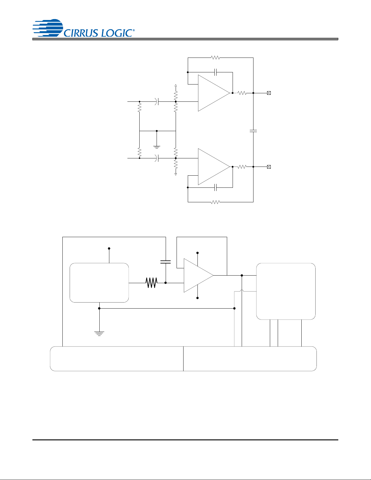
Figure 24. Single-Ended to Differential Active Input Filter ........................................................................ 36
Figure 25. Single-Ended to Differential Active Input Filter - DC Coupled Input Signal (VA/2 Centered) ... 36
Figure 26. DAC1-4 Path ............................................................................................................................ 37
Figure 27. De-emphasis Curve ................................................................................................................. 38
Figure 28. Passive Analog Output Filter ................................................................................................... 38
Figure 29. Volume Implementation for the DAC1-4 Path .......................................................................... 39
Figure 30. Soft Ramp Behavior ................................................................................................................. 40
Figure 31. Interrupt Behavior and Example Interrupt Service Routine ...................................................... 44
Figure 32. ADC Stopband Rejection ......................................................................................................... 59
Figure 33. ADC Transition Band ............................................................................................................... 59
Figure 34. ADC Transition Band (Detail) ................................................................................................... 59
Figure 35. ADC Passband Ripple ............................................................................................................. 59
Figure 36. ADC HPF (48 kHz) ................................................................................................................... 59
Figure 37. ADC HPF (96 kHz) ................................................................................................................... 59
Figure 38. SSM DAC Stopband Rejection ................................................................................................ 60
Figure 39. SSM DAC Transition Band ...................................................................................................... 60
Figure 40. SSM DAC Transition Band (Detail) .......................................................................................... 60
Figure 41. SSM DAC Passband Ripple .................................................................................................... 60
Figure 42. DSM DAC Stopband Rejection ................................................................................................ 61
Figure 43. DSM DAC Transition Band ...................................................................................................... 61
Figure 44. DSM DAC Transition Band (Detail) .......................................................................................... 61
Figure 45. DSM DAC Passband Ripple ............................................................................................
Figure 46. Package Drawing ..................................................................................................................... 62
CS4244
........ 61
DS900F1 3
Page 4

LIST OF TABLES
Table 1. Speed Modes .............................................................................................................................. 26
Table 2. Common Clock Frequencies ....................................................................................................... 26
Table 3. Master Mode Left Justified and I²S Clock Ratios ........................................................................ 27
Table 4. Slave Mode Left Justified and I²S Clock Ratios .......................................................................... 27
Table 5. Slave Mode TDM Clock Ratios ................................................................................................... 27
Table 6. Soft Ramp Rates ......................................................................................................................... 41
Table 7. Noise Gate Bit Depth Settings .................................................................................................... 41
Table 8. Error Reporting and Interrupt Behavior Details ........................................................................... 42
CS4244
DS900F1 4
Page 5
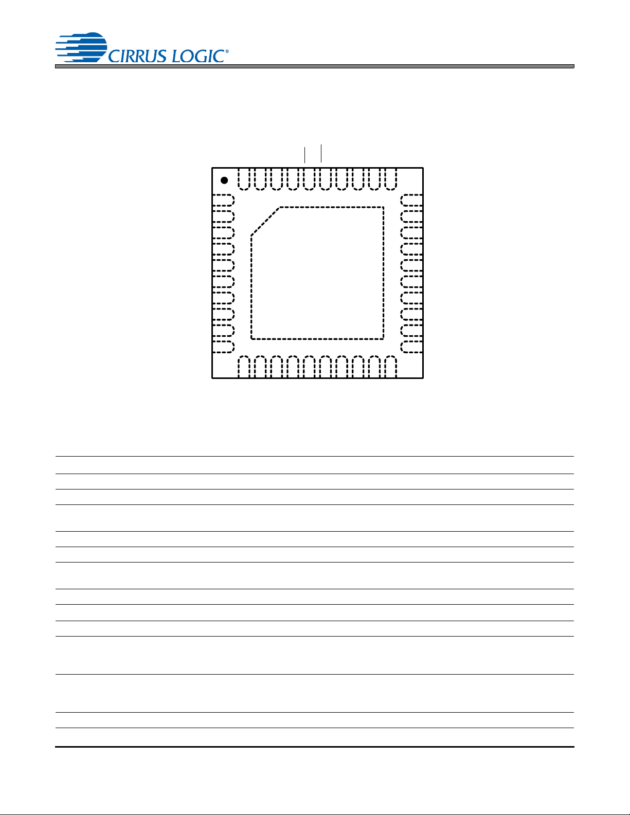
1. PIN DESCRIPTIONS
AD0
AD2/SDOUT2
TST O1
VA
AIN3+
AIN4-
AIN3-
AIN2+
AIN2-
AIN1-
AIN1+
FILT+
SDA
MCLK
SDOUT 1
VL
GND
SDIN1
SDIN2
12
11
13
14
15
16
17
18
19
20
29
30
28
27
26
25
24
23
22
21
394038
37
36
35
34
33
32
31
2
1
3
4
5
6
7
8
9
10
AOUT1+
SCLK
VDREG
AOUT2+
AOUT2-
AOUT3+
AOUT3-
AOUT4-
AOUT4+
VBIAS
VREF
VQ
GND
TST O2
AOUT1-
SCL
FS/LRCK
AD1
INT
RST
AIN4+
Top-Down
(Though Package)
View
CS4244
Figure 1. CS4244 Pinout
Pin Name Pin # Pin Description
SDA 1 Serial Control Data (Input/Output) - Bi-directional data I/O for the I²C control port.
SDINx 2,3 Serial Data Input (Input) - Input channels serial audio data.
FS/LRCK 4
MCLK 5 Master Clock (Input) -Clock source for the internal logic, processing, and modulators.
SCLK 6 Serial Clock (Input/Output) -Serial Clock for the serial data port.
SDOUT1 7
VL 8 Interface Power (Input) - Positive power for the digital interface level shifters.
GND 9,21
VDREG 10 Digital Power (Output) - Internally generated positive power supply for digital section.
AINx+
AINx-
FILT+ 19 Positive Voltage Reference (Output) - Positive reference voltage for the internal ADCs.
DS900F1 5
11,13,15,
12,14,16,
Frame Synchronization Clock/Left/Right Clock (Input/Output) - Determines which channel or
frame is currently active on the serial audio data line.
Serial Data Output 1 (Output) - ADC data output into a multi-slot TDM stream or AIN1 and AIN2
ADC data output in Left Justified and I²S modes.
Ground (Input) - Ground reference for the I/O and digital, analog sections.
Positive Analog Input (Input) - Positive input signals to the internal analog to digital converters. The
full scale analog input level is specified in the Analog Input Characteristics tables on pages 11 and
17
12.
Negative Analog Input (Input) - Negative input signals to the internal analog to digital converters.
The full scale analog input level is specified in the Analog Input Characteristics tables on pages 11
18
and 12.
Page 6
VA 20 Analog Power (Input) - Positive power for the analog sections.
VQ 22 Quiescent Voltage (Output) - Filter connection for internal quiescent voltage.
VREF 23 Analog Power Reference (Input) - Return pin for the VBIAS cap.
VBIAS 24 Positive Voltage Reference (Output) - Positive reference voltage for the internal DACs.
AOUTx-
AOUTx+
TSTOx 33,34 Test Outputs (Output) - Test outputs. These pins should be left unconnected.
RST
INT
AD2/SDOUT2 37
AD1 38 I²C Address Bit 1 (Input) - Sets the I²C address bit 1.
AD0 39 I²C Address Bit 0 (Input) - Sets the I²C address bit 0.
SCL 40 Serial Control Port Clock (Input) - Serial clock for the I²C control port.
GND -
25,27,29,
26,28,30,
Negative Analog Output (Output) - Negative output signals from the internal digital to analog con-
verters. The full scale analog output level is specified in the
31
on pages 15 and 16
Positive Analog Output (Output) - Positive output signals from the internal digital to analog convert-
ers. The full scale analog output level is specified in the Analog Output Characteristics tables on
32
pages 15 and 16
35 Reset (Input) - Applies reset to the internal circuitry when pulled low.
36 Interrupt (Output) - Sent to DSP to indicate an interrupt condition has occurred.
I²C Address Bit 2/Serial Data Output 2 (Input/Output) - Sets the I²C address bit 2 at reset. Func-
tions as Serial Data Out 2 for AIN3 and AIN4 ADC data output in Left Justified and I²S modes. High
impedance in TDM mode. See Section 4.3 I²C Control Port for more details concerning this mode of
operation.
Thermal Pad - The thermal pad on the bottom of the device should be connected to the ground
plane via an array of vias.
.
.
Analog Output Characteristics tables
CS4244
1.1 I/O Pin Characteristics
Input and output levels and associated power supply voltage are shown in the table below. Logic levels
should not exceed the corresponding power supply voltage.
Power Supply Pin Name I/O Driver
SCL Input - Weak Pull-down (~500k 5.0 V CMOS, with Hysteresis
SDA Input/Output
NT Output
I
RST
VL
Notes:
1. Internal connection valid when device is in reset.
2. This pin has no internal pull-up or pull-down resistors. External pull-up or pull-down resistors should
be added in accordance with Figure 2.
MCLK Input - Weak Pull-down (~500k 5.0 V CMOS, with Hysteresis
FS/LRCK Input/Output 5.0 V CMOS Weak Pull-down (~500k 5.0 V CMOS, with Hysteresis
SCLK Input/Output 5.0 V CMOS Weak Pull-down (~500k 5.0 V CMOS, with Hysteresis
SDOUT1 Output 5.0 V CMOS Weak Pull-down (~500k
SDINx Input - Weak Pull-down (~500k 5.0 V CMOS, with Hysteresis
AD0,1 Input - (Note 2) 5.0 V CMOS
AD2/SDOUT2 Input/Output 5.0 V CMOS (Note 2) 5.0 V CMOS
Internal Connections
(Note 1)
CMOS/Open
Drain
CMOS/Open
Drain
Input - (Note 2) 5.0 V CMOS, with Hysteresis
Weak Pull-down (~500k 5.0 V CMOS, with Hysteresis
(Note 2) -
Receiver
DS900F1 6
Page 7
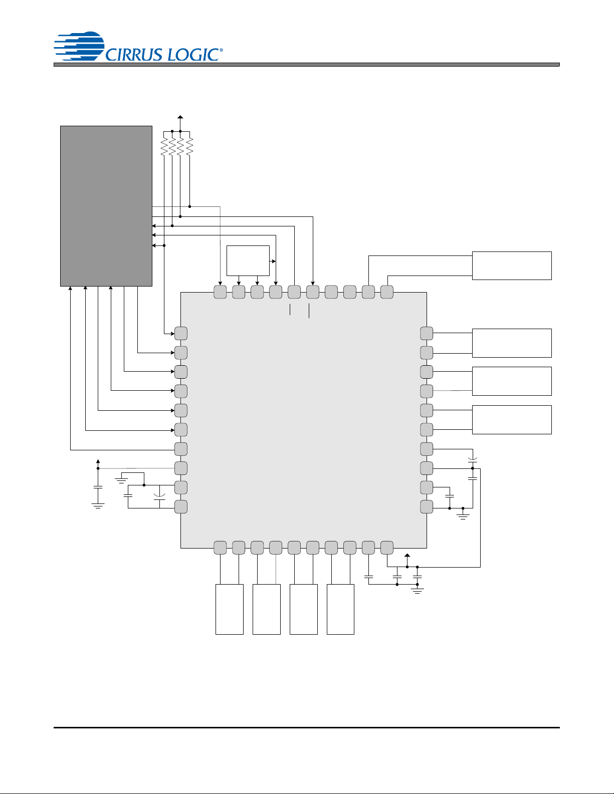
2. TYPICAL CONNECTION DIAGRAM
CS4244
AIN4-
AIN3+
AIN2-
AIN3-
VA
FILT+
AIN1+
AIN1-
AIN2+
AIN4+
SDOU T1
VL
GND
FS/LRCK
MCLK
SDIN 2
SDIN 1
SDA
VDREG
SCLK
AD2/ SDOUT 2
INT
AOUT 1-
TSTO2
AOUT 1+
TSTO1
RST
AD0
AD1
SCL
35
AOUT 3 -
AOUT 4 +
GND
VREF
VQ
VBIAS
AOUT 4 -
AOUT 2 -
AOUT 3 +
AOUT 2 +
32 31
+1.8 V to +5.0 V
0. 1uF
Pull U p or
Down Based
upon Desired
Address
***
0.1 uF
10 uF
Rp (x4)
40 38 37 3639
Digital Signal
Processor
1
3
2
6
4
5
7
8
VL
3334
30
28
27
26
25
22
29
23
0 .1uF 10 uF
+3 .3 V to
+5.0 V
1uF
20
24
10 uF
0 .1uF
10
9
19
21
Analog Output F ilter *
Analog Output F ilter *
Analog Output F ilter *
Analog In pu t
Filter **
11 12 1413
Analog In pu t
Filter **
Analog In pu t
Filter **
Analog In pu t
Filter **
17 1815 16
Analog Output F ilter *
10 uF
****
* See Section 4.6.4
** See Section 4.6.2.2
*** See Section 4.3
**** See Switching Specifications - Control Port
CS4244
DS900F1 7
Figure 2. Typical Connection Diagram
Page 8
CS4244
3. CHARACTERISTICS AND SPECIFICATIONS
RECOMMENDED OPERATING CONDITIONS
GND = 0 V; all voltages with respect to ground. (Note 3)
Parameters Symbol Min Typ Max Units
DC Power Supply
Analog Core VA
Level Translator VL 1.71 - 5.25 V
3.135
4.75
3.3
5
3.465
5.25
Temperature
Ambient Operating Temperature - Power Applied Automotive
Commercial
Junction Temperature T
T
A
J
-40
0
-40 - +150 C
-
-
+85
+70
C
C
Notes: 3. Device functional operation is guaranteed within these limits. Functionality is not guaranteed or
implied outside of these limits. Operation outside of these limits may adversely affect device reliability.
ABSOLUTE MAXIMUM RATINGS
GND = 0 V; all voltages with respect to ground.
V
V
Parameters Symbol Min Max Units
DC Power Supply
Analog Core VA -0.3 5.5 V
Level Translator VL -0.3 5.5 V
VDREG Current (Note 4) I
VDREG
-10A
Inputs
Input Current (Note 5) I
Analog Input Voltage (Note 6) V
Logic Level Input Voltage (Note 6) V
in
INA
IND
-±10mA
- 0.3 VA + 0.4 V
-0.3 VL + 0.4 V
Temperature
Ambient Operating Temperature - Power Applied T
Storage Temperature T
WARNING:
OPERATION BEYOND THESE LIMITS MAY RESULT IN PERMANENT DAMAGE TO THE DEVICE.
A
stg
-55 +125 °C
-65 +150 °C
Notes: 4. No external loads should be connected to the VDREG pin. Any connection of a load to this point may
result in errant operation or performance degradation in the device.
5. Any pin except supplies. Transient currents of up to ±100 mA on the analog input pins will not cause
SCR latch-up.
6. The maximum over/under voltage is limited by the input current.
DS900F1 8
Page 9
DC ELECTRICAL CHARACTERISTICS
GND = 0 V; all voltages with respect to ground.
Parameters Min Typ Max Units
VDREG (Note 7)
Nominal Voltage
Output Impedance
FILT+
Nominal Voltage
Output Impedance
DC Current Source/Sink
VQ
Nominal Voltage
Output Impedance
DC Current Source/Sink
Notes:
7. No external loads should be connected to the VDREG pin. Any connection of a load to this point may
result in errant operation or performance degradation in the device.
CS4244
-
-
-
-
-
-
-
-
2.5
0.5
VA
23
-
0.5•VA
77
-
-
-
-
-
1
-
-
0
V
V
k
A
V
k
A
DS900F1 9
Page 10
CS4244
TYPICAL CURRENT CONSUMPTION
This table represents the power consumption for individual circuit blocks within the CS4244. CS4244 is configured as
shown in Figure 2 on page 7. VA_SEL = 0 for VA = 3.3 VDC, 1 for VA = 5.0 VDC; F
DAC load is 3 k; All input signals are zero (digital zero for SDINx inputs and AC coupled to ground for AINx
inputs) .
Functional Block
Reset Overhead
1
(All lines held static, RST
Power Down Overhead
2
(All lines clocks and data lines active, RST
PLL (Note 10)
3
(Current drawn resulting from PLL being active. PLL is active for 256x and 384x)
DAC Overhead
4
(Current drawn whenever any of the four DACs are powered up.)
DAC Channel (Note 8)
5
(Current drawn per each DAC powered up.)
ADC Overhead
6
(Current drawn whenever any of the four ADCs are powered up.)
ADC Group
7
(Current drawn due to an ADC “group” being powered up. See
ADC Channel
8
(Current drawn per each ADC powered up.)
line pulled low.)
line pulled high, All PDNx bits set high.)
(Note 11))
= 100 kHz; MCLK = 25.6 MHz;
S
Typical Current [mA]
(unless otherwise noted)
(Note 9), (Note 12)
VA/ VL
5 0.030 0.001
3.3 0.020 0.001
5 5 0.101
3.3 5 0.101
51 -
3.3 1 550 -
3.3 45 55 -
3.3 4 511 -
3.3 11 52 -
3.3 2 5 2 0.109
3.3 2 0.066
i
VA
i
VL
Notes:
8. Full-scale differential output signal.
9. Current consumption increases with increasing F
and increasing MCLK. Values are based on FS of
S
100 kHz and MCLK of 25.6 MHz. Current variance between speed modes is small.
10. PLL is activated by setting the MCLK RATE bit to either 000 (operating in 256x mode) or 001 (operating
in 384kHz).
11. Internal to the CS4244, the analog to digital converters are grouped together in stereo pairs. ADC1 and
ADC2 are grouped together as are ADC3 and ADC4. The ADC group current draw is the current that
is drawn whenever one of these groups become active.
12. To calculate total current draw for an arbitrary amount of ADCs or DACs, the following equations apply:
Total Running Current Draw from VA Supply = Power Down Overhead + PLL (If Applicable)+ DAC Current Draw + ADC Current Draw
where
ADC Current Draw = ADC Overhead + (Number of active ADC Groups x ADC Group) + (Number of active ADC Channels x ADC Channel)
Total Running Current Draw from V
DAC Current Draw = DAC Overhead + (Number of DACs x DAC Channel)
and
L Supply = PDN Overhead + (Number of active ADC Channels x ADC Channel)
DS900F1 10
Page 11
CS4244
ANALOG INPUT CHARACTERISTICS (COMMERCIAL GRADE)
Test Conditions (unless otherwise specified): Device configured as shown in Section 2. on page 7. Input sine
wave: 1 kHz; VA_SEL = 0 for VA = 3.3 VDC, 1 for VA = 5.0 VDC.; T
20 kHz unless otherwise specified; Sample Rate = 48 kHz; all Power Down ADCx bits = 0.
VA, VREF = 3.3 V VA, VREF = 5.0 V
Parameter
Dynamic Range
Total Harmonic Distortion + Noise
Other Analog Characteristics
Interchannel Gain Mismatch - 0.2 - - 0.2 - dB
Gain Drift - ±100 - - ±100 Offset Error (Note 13)
Interchannel Isolation - 90 - - 90 - dB
Full-scale Input Voltage
(Differential Inputs) 1.58•VA 1.66•VA 1.74•VA 1.58•VA 1.66•VA 1.74•VA Vpp
Input Impedance - 40 - - 40 - k
Common Mode Rejection
(Differential Inputs)
PSRR (Note 14) 1 kHz
High Pass Filter On
High Pass Filter Off
A-weighted
unweighted
-1 dBFS
-60 dBFS
60 Hz
Min Typ Max Min Typ Max Unit
95
92
-
-
-
-
-60- -60- dB
-
-
101
98
-95
-38
0.0001
0.25
45
20
= 25 C; Measurement Bandwidth is 20 Hz to
A
-
-
-89
-32
-
-
-
-
99
96
105
102
-
-
-
-
-
-
-88
-42
0.0001
0.25
45
20
-
-
-82
-36
-
-
-
-
dB
dB
dB
dB
ppm/°C
% Full Scale
% Full Scale
dB
dB
DS900F1 11
Page 12

CS4244
ANALOG INPUT CHARACTERISTICS (AUTOMOTIVE GRADE)
Test Conditions (unless otherwise specified): Device configured as shown in Section 2. on page 7. Input sine
wave: 1 kHz; VA_SEL = 0 for VA = 3.3 VDC, 1 for VA = 5.0 VDC.; T
20 Hz to 20 kHz unless otherwise specified; Sample Rate = 48 kHz; all Power Down ADCx bits = 0.
VA, VREF = 3.3 V VA, VREF = 5.0 V
Parameter
Dynamic Range
Total Harmonic Distortion + Noise
Other Analog Characteristics
Interchannel Gain Mismatch - 0.2 - - 0.2 - dB
Gain Drift - ±100 - - ±100 Offset Error (Note 13)
Interchannel Isolation - 90 - - 90 - dB
Full-scale Input Voltage
(Differential Inputs) 1.58•VA 1.66•VA 1.74•VA 1.58•VA 1.66•VA 1.74•VA Vpp
Input Impedance - 40 - - 40 - k
Common Mode Rejection
(Differential Inputs)
PSRR (Note 14) 1 kHz
High Pass Filter On
High Pass Filter Off
A-weighted
unweighted
-1 dBFS
-60 dBFS
60 Hz
Min Typ Max Min Typ Max Unit
93
90
-
-
-
-
-60- -60- dB
-
-
101
98
-95
-38
0.0001
0.25
45
20
-87
-30
= -40 to +85 C; Measurement Bandwidth is
A
-
-
-
-
-
-
97
94
105
102
-
-
-
-
-
-
-88
-42
0.0001
0.25
45
20
-
-
-80
-34
-
-
-
-
dB
dB
dB
dB
ppm/°C
% Full Scale
% Full Scale
dB
dB
Notes:
13. AINx+ connected to AINx-.
14. Valid with the recommended capacitor values on FILT+ and VQ. See Figure 4 for test configuration.
DS900F1 12
Page 13
CS4244
100 k
4.7 uF
100 k
100 k
470 pF
634
90 .9
Analog Signal +
+
-
100 k
4.7 uF
100 k
100 k
470 pF
634
90 .9
Analog S ignal -
+
-
VA
VA
2700 pF
CS4244 AINx +
CS4244 AINx -
Operational
Amplifier
OUT
GND
Power DAC
Analog
Out
GND
PWR
DUT
+Vcc
+Vcc
+
-
OUT
Test Equipment
Analog Generator Analyzer
-Vcc
Digital
Out
+
-
+
-
+
-
Figure 3. Test Circuit for ADC Performance Testing
Figure 4. PSRR Test Configuration
DS900F1 13
Page 14
CS4244
ADC DIGITAL FILTER CHARACTERISTICS
Test Conditions (unless otherwise specified): Device configured as shown in Section 2. on page 7. Input sine
wave: 1 kHz; VA_SEL = 0 for VA = 3.3 VDC, 1 for VA = 5.0 VDC.; Measurement Bandwidth is 20 Hz to 20 kHz
unless otherwise specified. See filter plots in Section 7. on page 59.
Parameter (Note 15) Min Typ Max Unit
Passband (Frequency Response) to -0.1 dB corner 0 - 0.4535 Fs
Passband Ripple -0.09 - 0.17 dB
Stopband 0.6 - - Fs
Stopband Attenuation 70 - - dB
Single-Speed Mode
ADC Group Delay (Note 16) - 9.5/Fs - s
High-Pass Filter Characteristics (48 kHz Fs)
Frequency Response -3.0 dB
-0.13 dB
Phase Deviation @ 20 Hz - 10 - Deg
Passband Ripple -0.09 - 0.17 dB
Filter Settling Time (Note 17) -
Double-Speed Mode
ADC Group Delay (Note 16) - 9.5/Fs - s
High-Pass Filter Characteristics (96 kHz Fs)
Frequency Response -3.0 dB
-0.13 dB
Phase Deviation @ 20 Hz - 10 - Deg
Passband Ripple -0.15 - 0.17 dB
Filter Settling Time (Note 17)
-
-
-
-
-
2
11
25000/Fs
4
22
25000/Fs
-
-
0s
-
-
0s
Hz
Hz
Hz
Hz
Note:
15. Response is clock-dependent and will scale with Fs.
16. The ADC group delay is measured from the time the analog inputs are sampled on the AINx pins to
the FS/LRCK transition (rising or falling) after the last bit of that (group of) sample(s) has been
transmitted on SDOUTx.
17. The amount of time from input of half-full-scale step function until the filter output settles to 0.1% of
full scale.
DS900F1 14
Page 15
CS4244
ANALOG OUTPUT CHARACTERISTICS (COMMERCIAL GRADE)
Test Conditions (unless otherwise specified). Device configured as shown in Section 2. on page 7. VA_SEL = 0 for
VA = 3.3 VDC, 1 for VA = 5.0 VDC.; T
surement Bandwidth is 20 Hz to 20 kHz; Specifications apply to all channels unless otherwise indicated; all Power
Down DACx bits = 0. See (Note 19) on page 16.
= 25 C; Full-scale 1 kHz input sine wave; Sample Rate = 48 kHz; Mea-
A
VA, VREF= 3.3 V
(Differential/Single-ended)
Parameter Min Typ Max Min Typ Max Unit
Dynamic Performance
Dynamic Range
18 to 24-Bit A-weighted
unweighted
16-Bit A-weighted
unweighted
Total Harmonic Distortion + Noise - -90/-88 -84/-82 - -90/-88 -84/-82 dB
Full-scale Output Voltage
Interchannel Isolation (1 kHz) - 100 - - 100 - dB
Interchannel Gain Mismatch - 0.1 0.25 - 0.1 0.25 dB
Gain Drift - ±100 - - ±100 - ppm/°C
AC-Load Resistance (R
Load Capacitance (C
Parallel DC-Load Resistance(Note 20) 10 - - 10 - - k
Output Impedance - 100 - - 100 -
PSRR (Note 21) 1 kHz
)(Note 19) 3- -3- -k
L
)(Note 19) - - 100 - - 100 pF
L
60 Hz
100/96
97/93
89
86
1.48•VA/
0.74•VA
-
-
106/102
103/99
95
92
1.56•VA/
0.78•VA
60
60
-
-
-
-
1.64•VA/
0.82•VA
-
-
VA, VREF= 5.0 V
(Differential/Single-ended)
103/99
100/96
89
86
1.48•VA/
0.74•VA
-
-
109/105
106/102
95
92
1.56•VA/
0.78•VA
60
60
1.64•VA/
0.82•VA
-
-
-
-
-
-
dB
dB
dB
dB
Vpp
dB
dB
DS900F1 15
Page 16
CS4244
AOUTx
GND
22 µF
V
OUT
R
L
C
L
ANALOG OUTPUT CHARACTERISTICS (AUTOMOTIVE GRADE)
Test Conditions (unless otherwise specified): Device configured as shown in Section 2. on page 7. VA_SEL = 0 for
VA = 3.3 VDC, 1 for VA = 5.0 VDC.; T
Measurement Bandwidth is 20 Hz to 20 kHz; Specifications apply to all channels unless otherwise indicated; all
Power Down DACx bits = 0. See (Note 19).
= -40 to +85 C; Full-scale 1 kHz input sine wave; Sample Rate = 48 kHz;
A
VA, VREF= 3.3 V
(Differential/Single-ended)
VA, VREF= 5.0 V
(Differential/Single-ended)
Parameter Min Typ Max Min Typ Max Unit
Dynamic Performance
Dynamic Range
18 to 24-Bit A-weighted
unweighted
16-Bit A-weighted
unweighted
98/94
95/91
87
84
106/102
103/99
95
92
-
-
-
-
101/97
98/94
87
84
109/105
106/102
95
92
-
-
-
-
dB
dB
dB
dB
Total Harmonic Distortion + Noise - -90/-88 -82/-80 - -90/-88 -82/-80 dB
Full-scale Output Voltage
1.48•VA/
0.74•VA
1.56•VA/
0.78•VA
1.64•VA/
0.82•VA
1.48•VA/
0.74•VA
1.56•VA/
0.78•VA
1.64•VA/
0.82•VA
Vpp
Interchannel Isolation (1 kHz) - 100 - - 100 - dB
Interchannel Gain Mismatch - 0.1 0.25 - 0.1 0.25 dB
Gain Drift - ±100 - - ±100 - ppm/°C
AC-Load Resistance (R
Load Capacitance (C
)(Note 19) 3- -3--k
L
)(Note 19) - - 100 - - 100 pF
L
Parallel DC-Load Resistance(Note 20) 10 - - 10 - - k
Output Impedance - 100 - - 100 -
PSRR (Note 21) 1 kHz
60 Hz
-
-
60
60
-
-
-
-
60
60
-
-
dB
dB
Notes:
18. One LSB of triangular PDF dither added to data.
19. Loading configuration is given in Figure 5 below.
Figure 5. Equivalent Output Test Load
20. Parallel combination of all DAC DC loads. See Section 4.2.3.
21. Valid with the recommended capacitor values on FILT+ and VQ. See Figure 4 for test configuration.
DS900F1 16
Page 17
CS4244
COMBINED DAC INTERPOLATION & ON-CHIP ANALOG FILTER RESPONSE
Test Conditions (unless otherwise specified): VA_SEL = 0 for VA = 3.3 VDC, 1 for VA = 5.0 VDC. The filter characteristics have been normalized to the sample rate (F
plying the given characteristic by F
.
S
Parameter Min Typ Max Unit
Single-Speed Mode
Passband (Note 22) to -0.05 dB corner
Frequency Response 20 Hz to 20 kHz -0.01 - +0.12 dB
StopBand 0.5465 - - F
StopBand Attenuation (Note 23) 102 - - dB
DAC1-4 Group Delay (Note 24) -11/Fs-s
Double-Speed Mode
Passband (Note 22) to -0.1 dB corner
Frequency Response 20 Hz to 20 kHz -0.05 - +0.2 dB
StopBand 0.5770 - - F
StopBand Attenuation (Note 23) 80 - - dB
DAC1-4 Group Delay (Note 24) -7/Fs-s
) and can be referenced to the desired sample rate by multi-
S
to -3 dB corner
to -3 dB corner
0
0
0
0
-
-
-
-
0.4780
0.4996
0.4650
0.4982
F
S
F
S
S
F
S
F
S
S
Notes:
22. Response is clock-dependent and will scale with F
23. For Single-Speed Mode, the measurement bandwidth is 0.5465 F
For Double-Speed Mode, the measurement bandwidth is 0.577 F
.
S
to 3 FS.
S
to 1.4 FS.
S
24. The DAC group delay is measured from the FS/LRCK transition (rising or falling) before the first bit of
a (group of) sample(s) is transmitted on the SDINx pins to the time it appears on the AOUTx pins.
DS900F1 17
Page 18
CS4244
DIGITAL I/O CHARACTERISTICS
Parameters Symbol Min Typ Max Units
High-Level Input Voltage (all input pins except
(VL=1.8V)
High-Level Input Voltage (all input pins except
(VL=2.5V, 3.3V, or 5V)
Low-Level Input Voltage (all input pins except
High-Level Input Voltage (
Low-Level Input Voltage (
High-Level Output Voltage at I
Low-Level Output Voltage at I
RST pin) V
RST pin) V
=2mA (% of VL) V
o
=2mA (% of VL) V
o
Input Leakage Current I
Input Capacitance - 8 - pF
RST)(% of VL)
RST)(% of VL)
RST)(% of VL)V
V
IH
V
IH
IL
IH
IL
OH
OL
in
75% - - V
70% - - V
--30%V
1.2 - - V
--0.3V
80% - - V
--20%V
--±10A
DS900F1 18
Page 19
CS4244
SWITCHING CHARACTERISTICS - SERIAL AUDIO INTERFACE
VA_SEL = 0 for VA = 3.3 VDC, 1 for VA = 5.0 VDC.
Parameters Symbol Min Max Units
RST pin Low Pulse Width (Note 25) 1
MCLK Frequency
(Note 26) 7.68 25.6 MHz
MCLK Duty Cycle 45 55 %
SCLK Duty Cycle 45 55 %
Input Sample Rate (FS/LRCK pin) Single-Speed Mode
Double-Speed Mode
SCLK Falling Edge to SDOUTx Valid (VL = 1.8 V) t
SCLK Falling Edge to SDOUTx Valid (VL = 2.5 V) t
SCLK Falling Edge to SDOUTx Valid (VL = 3.3 V or 5 V) t
F
F
dh2
dh2
dh2
S
S
30
60
-31ns
-22ns
-17ns
TDM Slave Mode
SCLK Frequency
FS/LRCK High Time Pulse (Note 28)
FS/LRCK Rising Edge to SCLK Rising Edge t
SDINx Setup Time Before SCLK Rising Edge t
SDINx Hold Time After SCLK Rising Edge t
(Note 27) 256x 512x F
t
lpw
lcks
dh1
ds
1/f
SCLK
5-ns
3-ns
5-ns
PCM Slave Mode
SCLK Frequency 32x 64x F
FS/LRCK Duty Cycle 45 55 %
FS/LRCK Edge to SCLK Rising Edge t
SDINx Setup Time Before SCLK Rising Edge t
SDINx Hold Time After SCLK Rising Edge t
lcks
ds
dh1
5-ns
3-ns
5-ns
PCM Master Mode
SCLK Frequency 64x 64x F
FS/LRCK Duty Cycle 45 55 %
FS/LRCK Edge to SCLK Rising Edge t
SDINx Setup Time Before SCLK Rising Edge t
SDINx Hold Time After SCLK Rising Edge
(VL=1.8V)
SDINx Hold Time After SCLK Rising Edge
(VL=2.5V, 3.3V, or 5V)
lcks
t
dh1
t
dh1
ds
5-ns
5-ns
11 - ns
10 - ns
-ms
50
100
(n-1)/f
SCLK
(Note 29)
kHz
kHz
S
ns
S
S
Notes:
25. After applying power to the
CS4244, RST should be held low until after the power supplies and MCLK
are stable.
26. MCLK must be synchronous to and scale with F
.
S
27. The SCLK frequency must remain less than or equal to the MCLK frequency. For this reason, SCLK
may range from 256x to 512x only in single speed mode. In double speed mode, 256x is the only ratio
supported.
28. The MSB of CH1 is always aligned with the second SCLK rising edge following FS/LRCK rising edge.
29. Where “n” is equal to the MCLK to LRCK ratio (set by the Master Clock Rate register bits), i.e. in 256x
mode, n = 256, in 512x mode, n = 512, etc.
DS900F1 19
Page 20

CS4244
SDOUT1
(output )
SDINx
(input )
t
ds
SCLK
(input )
FS/LRCK
(input )
MSB
t
dh1
MSB-1
t
lcks
t
dh2
MSB MSB-1
t
dh2
t
LPW
~~~
t
ds
MSB
t
dh1
t
dh2
MSB-1
t
lcks
FS/LRCK
(input /output)
SCLK
(input /output)
SDINx
(input)
SDOUTx
(output)
MSB
MSB-1
Figure 7. PCM Serial Audio Interface Timing
Figure 6. TDM Serial Audio Interface Timing
DS900F1 20
Page 21

CS4244
t
buf
t
hdst
t
hdst
t
low
t
r
t
f
t
hdd
t
high
t
sud
t
sust
t
susp
Stop Start
Start
Stop
Repeated
SDA
SCL
t
irs
RST
Figure 8. I²C Control Port Timing
SWITCHING SPECIFICATIONS - CONTROL PORT
Test conditions (unless otherwise specified): Inputs: Logic 0 = GND = 0 V, Logic 1 = VL; SDA load capacitance equal to maximum value of Cb specified below (Note 30).
Parameters Symbol Min Max Unit
SCL Clock Frequency f
RESET
Bus Free Time Between Transmissions t
Start Condition Hold Time (prior to first clock pulse) t
Clock Low time t
Clock High Time t
Setup Time for Repeated Start Condition t
SDA Input Hold Time from SCL Falling (Note 32) t
SDA Output Hold Time from SCL Falling t
SDA Setup time to SCL Rising t
Rise Time of SCL and SDA t
Fall Time SCL and SDA t
Setup Time for Stop Condition t
SDA Bus Load Capacitance
SDA Pull-Up Resistance
Rising Edge to Start t
scl
irs
buf
hdst
low
high
sust
hddi
hddo
sud
r
f
susp
C
R
p
b
- 550 kHz
(Note 31) -ns
1.3 - µs
0.6 - µs
1.3 - µs
0.6 - µs
0.6 - µs
00.9µs
0.2 0.9 µs
100 - ns
-300ns
-300ns
0.6 - µs
-400pF
500 -
Notes:
30. All specifications are valid for the signals at the pins of the CS4244 with the specified load capacitance.
31. 2 ms + (3000/MCLK). See Section 4.2.1.
32. Data must be held for sufficient time to bridge the transition time, t
, of SCL.
f
DS900F1 21
Page 22

4. APPLICATIONS
4.1 Power Supply Decoupling, Grounding, and PCB Layout
As with any high-resolution converter, the CS4244 requires careful attention to power supply and grounding
arrangements if its potential performance is to be realized. Figure 2 shows the recommended power arrangements, with VA connected to clean supplies. VDREG, which powers the digital circuitry, is generated
internally from an on-chip regulator from the VA supply. The VDREG pin provides a connection point for the
decoupling capacitors, as shown in Figure 2.
Extensive use of power and ground planes, ground plane fill in unused areas and surface mount decoupling
capacitors are recommended. Decoupling capacitors should be as near to the pins of the CS4244 as possible. The low value ceramic capacitor should be the nearest to the pin and should be mounted on the same
side of the board as the CS4244 to minimize inductance effects. All signals, especially clocks, should be
kept away from the FILT+, VBIAS, and VQ pins in order to avoid unwanted coupling into the modulators.
The FILT+, VBIAS, and VQ decoupling capacitors, particularly the 0.1 µF, must be positioned to minimize
the electrical path from their respective pins and GND.VA_SEL
For optimal heat dissipation from the package, it is recommended that the area directly under the device be
filled with copper and tied to the ground plane. The use of vias connecting the topside ground to the backside ground is also recommended.
4.2 Recommended Power-up & Power-down Sequence
CS4244
The initialization and Power-Up/Down sequence flow chart is shown in Figure 9. For the CS4244 Reset is
defined as all lines held static,
held static,
RST line is high, all PDNx bits are ‘1’. Running is defined as RST line high, all PDNx bits are ‘0’.
4.2.1 Power-up
The CS4244 enters a reset state upon the initial application of VA and VL. When these power supplies
are initially applied to the device, the audio outputs, AOUTxx, are clamped to VQ which is initially low.
Additionally, the interpolation and decimation filters, delta-sigma modulators and control port registers are
all reset and the internal voltage reference, multi-bit digital-to-analog and analog-to-digital converters and
low-pass filters are powered down. The device remains in the reset state until the
Once
RST is brought high, the control port address is latched after 2 ms + (3000/MCLK). Until this latching
transition is complete, the device will not respond to I²C reads or writes, but the I²C bus may still be used
during this time. Once the latching transition is complete, the address is latched and the control port is
accessible. At this point and the desired register settings can be loaded per the interface descriptions detailed in the Section 4.3 I²C Control Port. To ensure specified performance and timing, the VA_SEL must
be set to “0” for VA = 3.3 VDC and “1” for VA = 5.0 VDC before audio output begins.
After the
nominal quiescent voltage. VQ will charge to VA/2 upon initial power up. The time that it takes to charge
up to VA/2 is governed by the size of the capacitor attached to the VQ pin. With the capacitor value shown
in the typical connection diagram, the charge time will be approximately 250 ms. The gradual voltage
ramping allows time for the external DC-blocking capacitors to charge to VQ, effectively blocking the quiescent DC voltage. Once FS/LRCK is valid, MCLK occurrences are counted over one F
mine the MCLK/F
references will transition to their nominal voltage. Power is applied to the D/A converters and filters, and
the analog outputs are un-clamped from the quiescent voltage, VQ. Afterwards, normal operation begins.
RST pin is brought high and MCLK is applied, the outputs begin to ramp with VQ towards the
RST line is pulled low. Power Down is defined as all lines (excluding MCLK)
RST pin is brought high.
period to deter-
ratio. With MCLK valid and any of the PDNx bits cleared, the internal voltage
S
S
DS900F1 22
Page 23

CS4244
System
Operational
System
Unpowered
Set all PDN DAC & ADC bits
Stop SCLK, FS/LRCK, SDINx
Set VQ _RAMP b it
Remove VL, VA, and MCLK
Set Mute ADCx bits
Clear RST
DACx Fully
Operational
ADC Data
Available on
SDOUT x
2 ms + (3000/MCLK)
50 ms
Apply VL , VA, an d MCL K
Clear PDN DACx & ADCx bits
Start SCLK, FS/LRCK, SDINx
Write all req uired configu rat ion
settings to Control Port
Clear Mute DACx bits
Clear Mute ADCx bits
Set RST
VCM Re ady
(>90% of Typical)
I2C Address
Captured & Control
Port Rea dy
250 ms
Write VA_SEL bit (in 0Fh)
appropriately for VA
delay dependent
on DAC mute /
unmute behav ior
Set Mute DACx bits
delay dependent
on DAC mute/
unmute behav ior
2 ms +
(3000 /M CLK )
250 ms
4.2.2 Power-down
To prevent audio transients at power-down, the DC-blocking capacitors must fully discharge before turning off the power. In order to do this in a controlled manner, it is recommended that all the converters be
muted to start the sequence. Next, set PDNx for all converters to 1 to power them down internally. Then,
FS/LRCK and SCLK can be removed if desired. Finally, the “VQ RAMP” bit in the "DAC Control 4" register
must be set to ‘1’ for a period of 50 ms before applying reset or removing power or MCLK. During this
time, voltage on VQ and the audio outputs discharge gradually to GND. If power is removed before this
50 ms time period has passed, a transient will occur and a slight click or pop may be heard. There is no
minimum time for a power cycle. Power may be re-applied at any time.
It is important to note that all clocks should be applied and removed in the order specified in Figure 9. If
MCLK is removed or applied before
result. If either SCLK or FS/LRCK is removed or applied before all PDNx bits are set to 1, audible pops,
clicks and/or distortion can result.
Note: Timings are approximate and based upon the nominal value of the passive components specified in the
“Typical Connection Diagram” on page 7. See Section 4.6.5.2 for volume ramp behavior.
RST has been pulled low, audible pops, clicks and/or distortion can
4.2.3 DAC DC Loading
DS900F1 23
Figure 9. System Level Initialization and Power-Up/Down Sequence
Figure 10 shows the analog output configuration during power-up, with the AOUTx± pins clamped to VQ
to prevent pops and clicks. Thus any DC loads (RL
es are closed. These DC loads will pull the VQ voltage down towards ground. If the parallel combination
of all DC loads exceeds the specification shown in the Analog Output Characteristics tables on pages 15
) on the output pins will be in parallel when the switch-
x
Page 24

CS4244
~140kΩ
VA
VQ
NET
~140 kΩ
S1±
RL
1+
CL
1+
AOUT1+
RL
1-
CL
1-
AOUT1-
S2±
RL
2+
CL
2+
AOUT2+
RL
2-
CL
2-
AOUT2-
S3±
RL
3+
CL
3+
AOUT3+
RL
3-
CL
3-
AOUT3-
S4±
RL
4+
CL
4+
AOUT4+
RL
4-
CL
4-
AOUT4-
External VQ
capacitor
and 16, the VQ voltage will never rise to its minimum operating voltage. If the VQ voltage never rises
above this minimum operating voltage, the device will not finish the power-up sequence and normal operation will not begin.
Also note that any AOUTx± pin(s) with a DC load must remain powered up (PDN DACx = 0) to keep the
VQ net at its nominal voltage during normal operation, otherwise clipping may occur on the outputs.
Note that the load capacitors (CL
) are also in parallel during power-up. The amount of total capacitance
x
on the VQ net during power-up will affect the amount of time it takes for the VQ voltage to rise to its nominal operating voltage after VA power is applied. The time period can be calculated using the time constant
given by the internal series resistor and the load capacitors.
4.3 I²C Control Port
All device configuration is achieved via the I²C control port registers as described in the Switching Specifi-
cations - Control Port table. The operation via the control port may be completely asynchronous with respect
to the audio sample rates. However, to avoid potential interference problems, the I²C pins should remain
static if no operation is required. The CS4244 acts as an I²C slave device.
DS900F1 24
SDA is a bidirectional data line. Data is clocked into and out of the device by the clock, SCL. The AD0 and
AD1 pins form the two least significant bits of the chip address and should be connected through a resistor
to VL or GND as desired. The SDOUT2 pin is used to set the AD2 bit by connecting a resistor from the
SDOUT2 pin to VL or to GND. The state of these pins are sensed after the
Figure 10. DAC DC Loading
CS4244 is released from reset.
Page 25

CS4244
4 5 6 7 24 25
SCL
CHIP ADDRESS (WRITE) MAP BYTE DATA
DATA +1
START
ACK
STOP
ACKACKACK
0 0 1 0 AD2 A D1 AD0 0
SDA
INCR
6 5 4 3 2 1 0 7 6 1 0 7 6 1 0 7 6 1 0
0 1 2 3 8 9 1 2 16 1 7 1 8 19 10 11 13 14 15 27 2826
DATA +n
Figure 11. Timing, I²C Write
SCL
CHIP ADDRESS (WRITE) MAP BYTE
DATA
DATA +1
START
ACK
STOP
ACK
ACK
ACK
0 0 1 0 A D2 AD1 AD0 0
SDA
CHIP ADDRESS (READ)
START
INCR
6 5 4 3 2 1 0 7 0 7 0 7 0
NO
16 8 9 1 2 13 14 15 4 5 6 7 0 1 20 2 1 22 23 2 4
26 27 28
2 3 10 11 17 1 8 19 2 5
ACK
DATA + n
STOP
0 0 1 0 A D2 AD1 AD0 1
Figure 12. Timing, I²C Read
The signal timings for a read and write cycle are shown in Figure 11 and Figure 12. A Start condition is defined as a falling transition of SDA while the clock is high. A Stop condition is a rising transition while the
clock is high. All other transitions of SDA occur while the clock is low. The first byte sent to the
a Start condition consists of a 7-bit chip address field and a R/W
upper 4 bits of the 7-bit address field are fixed at 0010. To communicate with a
field, which is the first byte sent to the
The eighth bit of the address is the R/W
CS4244, should match 0010 followed by the settings of the ADx pins.
bit. If the operation is a write, the next byte is the Memory Address
bit (high for a read, low for a write). The
CS4244, the chip address
Pointer (MAP) which selects the register to be read or written. If the operation is a read, the contents of the
register pointed to by the MAP will be output. Setting the auto increment bit in MAP allows successive reads
or writes of consecutive registers. Each byte is separated by an acknowledge bit. The ACK bit is output from
the
CS4244 after each input byte is read, and is input to the CS4244 from the microcontroller after each trans-
mitted byte.
CS4244 after
Since the read operation can not set the MAP, an aborted write operation is used as a preamble. As shown
in Figure 12, the write operation is aborted after the acknowledge for the MAP byte by sending a stop condition. The following pseudocode illustrates an aborted write operation followed by a read operation.
Send start condition.
Send 0010xxx0 (chip address & write operation).
Receive acknowledge bit.
Send MAP byte, auto increment off.
Receive acknowledge bit.
Send stop condition, aborting write.
Send start condition.
Send 0010xxx1 (chip address & read operation).
Receive acknowledge bit.
Receive byte, contents of selected register.
Send acknowledge bit.
Send stop condition.
Setting the auto increment bit in the MAP allows successive reads or writes of consecutive registers. Each
byte is separated by an acknowledge bit.
DS900F1 25
Page 26

4.3.1 Memory Address Pointer (MAP)
The MAP byte comes after the address byte and selects the register to be read or written. Refer to the
pseudocode above for implementation details.
4.3.1.1 Map Increment (INCR)
The CS4244 has MAP auto-increment capability enabled by the INCR bit (the MSB) of the MAP. If INCR
is set to ‘0’, MAP will stay constant for successive I²C reads or writes. If INCR is set to ‘1’, MAP will autoincrement after each byte is read or written, allowing block reads or writes of successive registers.
4.4 System Clocking
The CS4244 will operate at sampling frequencies from 30 kHz to 100 kHz. This range is divided into two
speed modes as shown in Table 1.
Mode Sampling Frequency
Single-Speed 30-50 kHz
Double-Speed 60-100 kHz
Table 1. Speed Modes
The serial port clocking must be changed while all PDNx bits are set. If the clocking is changed otherwise,
the device will enter a mute state, see Section 4.8 on page 42.
CS4244
4.4.1 Master Clock
The ratio of the MCLK frequency to the sample rate must be an integer. The FS/LRCK frequency is equal
to F
, the frequency at which all of the slots of the TDM stream or channels in Left Justified or I²S formats
S
are clocked into or out of the device. The Speed Mode and Master Clock Rate bits configure the device
to generate the proper clocks in Master Mode and receive the proper clocks in Slave Mode. Table 2 illustrates several standard audio sample rates and the required MCLK and FS/LRCK frequencies.
The CS4244 has an internal fixed ratio PLL. This PLL is activated when the “MCLK RATE[2:0]” bits in the
"Clock & SP Sel." register are set to either 000 or 001, corresponding to 256x or 384x. When in either of
these two modes, the PLL will activate to adjust the frequency of the incoming MCLK to ensure that the
internal state machines operate at a nominal 24.576 MHz rate. As is shown in the Typical Current Con-
sumption table, activation of the PLL will increase the power consumption of the CS4244.
FS/LRCK (kHz) MCLK (MHz)
32 - -
44.1 - -
48 - -
64 8.1920 12.2880 16.3840
88.2 11.2896 16.9344 22.5792
96 12.2880 18.4320 24.5760
Mode
128x
(Note 33)
192x
(Note 33)
DSM
256x 384x 512x
8.1920 12.2880 16.3840
11.2896 16.9344 22.5792
12.2880 18.4320 24.5760
- -
- -
- -
SSM
Table 2. Common Clock Frequencies
Note:
33. 128x and 192x ratios valid only in Left Justified or I²S formats.
DS900F1 26
Page 27

4.4.2 Master Mode Clock Ratios
÷512
÷256
÷8
÷4
00
01
00
01
FS/LRCK
SCLK
000
001
010
x2
÷1.5
÷1
MCLK Speed M ode Bi ts
MC LK Rate Bits
x2
PLL active
Figure 13. Master Mode Clocking
As a clock master, FS/LRCK and SCLK will operate as outputs internally derived from MCLK. FS/LRCK
is equal to F
Mode.
The resulting valid master mode clock ratios are shown in Table 3 below.
MCLK/F
SCLK/F
and SCLK is equal to 64x FS as shown in Figure 13. TDM format is not supported in Master
S
S
S
CS4244
SSM DSM
256x, 384x, 512x 128x, 192x, 256x
64x 64x
Table 3. Master Mode Left Justified and I²S Clock Ratios
4.4.3 Slave Mode Clock Ratios
In Slave Mode, SCLK and FS/LRCK operate as inputs. The FS/LRCK clock frequency must be equal to
the sample rate, F
The serial bit clock, SCLK, must be synchronously derived from the master clock, MCLK, and be equal to
512x, 256x, 128x, 64x, 48x or 32x F
and Table 5 for required clock ratios.
MCLK/F
SCLK/F
S
S
(Note 34) SSM DSM
MCLK/F
SCLK/F
S
S
Note:
34. For all cases, the SCLK frequency must be less than or equal to the MCLK frequency.
, and must be synchronously derived from the supplied master clock, MCLK.
S
Table 4. Slave Mode Left Justified and I²S Clock Ratios
, depending on the desired format and speed mode. Refer to Table 4
S
SSM DSM
256x, 384x, 512x 128x, 192x, 256x
32x, 48x, 64x, 128x 32x, 48x, 64x
256x, 384x, 512x 512x 256x
256x 512x 256x
Table 5. Slave Mode TDM Clock Ratios
DS900F1 27
Page 28

4.5 Serial Port Interface
SCLK
SDINx & SDOUT1
Channel 1 Channel 2
Channel N-1 Channel N
FS/LRCK
Frame
(N ≤ 16)
Figure 14. TDM System Clock Format
MSB
32-Bit Channel Block
LSB
24-Bit Audio Word
8-Bit Zero Pad
-1
-2
-3
-4 -5
-6
-7
+1
+2
+3
Figure 15. 32-bit Receiver Channel Block
The serial port interface format is selected by the Serial Port Format register bits. The TDM format is available in Slave Mode only.
4.5.1 TDM Mode
The serial port of the CS4244 supports the TDM interface format with varying bit depths from 16 to 24 as
shown in Figure 15. Data is clocked out of the ADC on the falling edge of SCLK and clocked into the DAC
on the rising edge.
As indicated in Figure 15, TDM data is received most significant bit (MSB) first, on the second rising edge
of the SCLK occurring after a FS/LRCK rising edge. All data is valid on the rising edge of SCLK. All bits
are transmitted on the falling edge of SCLK. Each slot is 32 bits wide, with the valid data sample left justified within the slot. Valid data lengths are 16, 18, 20, or 24 bits.
CS4244
FS/LRCK identifies the start of a new frame and is equal to the sample rate, F
. As shown in Figure 14,
S
FS/LRCK is sampled as valid on the rising SCLK edge preceding the most significant bit of the first data
sample and must be held valid for at least 1 SCLK period.
The structure in which the serial data is coded into the TDM slots is shown in Figure 16. SDOUT2 is unused in TDM mode and is placed in a high-impedance state. When using a 48 kHz sample rate with a
24.576 MHz MCLK and SCLK, a 16 slot TDM structure can be realized. When using a 48 kHz sample rate
with 12.288 MHz SCLK and 24.576 MHz MCLK, or a 96 kHz sample rate with a 24.576 MHz MCLK and
SCLK, an 8 slot TDM structure can be realized. The data that is coded into the TDM slots is extracted into
the appropriate signal path via the settings in the Control port. Please refer to Section 4.6.1 Routing the
Serial Data within the Signal Paths for more details.
DS900F1 28
Page 29

CS4244
SDIN1
Input Data
[31:8]
[7:0]
Input Data
1.2
[31:8]
[7:0]
Input Data
1.3
[31:8]
[7:0]
Input Data
1.4
[31:8]
[7:0]
Input Data
1.5
[31:8]
[7:0]
Input Data
1.6
[31:8]
[7:0]
Input Data
1.7
[31:8]
[7:0]
Input Data
1.8
[31:8]
[7:0]
SDIN2
Input Data
[31:8]
[7:0]
Input Data
[31:8]
[7:0]
Input Data
2.3
[31:8]
x[7:0]
Input Data
2.4
[31:8]
[7:0]
Input Data
[31:8]
[7:0]
Input Data
[31:8]
x[7:0]
Input Data
2.7
[31:8]
x[7:0]
Input Data
[31:8]
x[7:0]
SDOUT1
ADC1
Data[31:8]
[7:0]
ADC2 Data
[31:8]
[7:0]
ADC3 Data
[31:8]
[7:0]
ADC4
Data[31:8]
[7:0]
SDOUT1
with
Sidechain
ADC1
Data[31:8]
[7:0]
ADC2 Data
[31:8]
[7:0]
ADC3 Data
[31:8]
[7:0]
ADC4 Data
[31:8]
[7:0]
MCLK = 12.288/24.576MHz
FS/LRCK = 48/96kHz
SCLK = 12.288/24.576MHz
Slot 1 [31:0] Slot 2 [31:0] Slot 3 [31:0] Slot 4 [31:0] Slot 5 [31:0] Slot 6 [31:0] S lot 7 [31:0] Slot 8 [31:0]
[31:0]
[31:0]
[31:0]
[31:0]
(SDIN2 Slot 1)
(SDIN2 Slot 2)
(SDIN2 Slot 3)
(SDIN2 Slot 4)
SDIN1
Input Data
[31:8]
[7:0]
Input Data
1.4
[31:8]
[7:0]
Input Data
1.5
[31:8]
[7:0]
Input Data
1.8
[31:8]
[7:0]
Input Data
[31:8]
[7:0]
Input Data
1.12
[31:8]
[7:0]
Input Data
[31:8]
[7:0]
Input Data
1.16
[31:8]
[7:0]
SDIN2
Input Data
[31:8]
[7:0]
Input Data
[31:8]
[7:0]
Input Data
[31:8]
[7:0]
Input Data
[31:8]
[7:0]
Input Data
[31:8]
[7:0]
Input Data
[31:8]
[7:0]
Input Data
[31:8]
[7:0]
Input Data
[31:8]
[7:0]
SDOUT1
ADC1 Data
[31:8]
[7:0]
ADC4 Data
[31:8]
[7:0]
SDOUT1
with
Sidechain
ADC1 Data
[31:8]
[7:0]
ADC4 Data
[31:8]
[7:0]
MCLK = 24.576MHz
FS/LRCK = 48kHz
[31:0]
(SDIN2 Slot 1)
SCLK = 24.576MHz
Slot 1 [31:0]
…→…
Slot 4 [31:0] Slot 5 [31:0]
…→…
Slot 8 [31:0] Slot 9 [31:0] Slot 13 [31:0]
…→…
Slot 16 [31:0]
[31:0]
[31:0]
[31:0]
[31:0]
[31:0]
…→…
Slot 12 [31:0]
(SDIN2 Slot 12)
(SDIN2 Slot 4)
(SDIN2 Slot 5)
(SDIN2 Slot 8)
(SDIN2 Slot 9)
Figure 16. Serial Data Coding and Extraction Options within the TDM Streams
x
x
0's
2.8
Output Data
x
0's
2.16
Output Data
x
0's
x
x
2.6
x
Output Data
0's
Output Data
0's
2.5
x
x
x
x
x
x
2.2
x
Output Data
0's
0's
0's
0's
0's
0's
0's
0's
x
1.13
x
x
1.9
x
x
x
x
x
2.13
x
2.12
x
2.9
x
2.8
x
2.5
x
2.4
x
0's
0's
0's
0's
0's
0's
0's
Output Data
Output Data
Output Data
Output Data
Output Data
0's
0's
DS900F1 29
1.1
2.1
1.1
2.1
Page 30

4.5.2 Left Justified and I²S Modes
FS/LRCK
SCLK
MSB LS B MSB LSB
AOUT 1 or 3
Left Channel Right Channel
SDOUTx
SDINx
AOUT 2 or 4
MSB
AIN 1 or 3
AIN 2 or 4
Figure 17. Left Justified Format
FS/LRCK
SCLK
MSB LSB MSB LSB
AOU T 1 or 3
Left Channel Right Channel
SDOUTx
SDINx
AOUT 2 or 4
MSB
AIN 1 or 3
AIN 2 or 4
Figure 18. I²S Format
The serial port of the CS4244 supports the Left Justified and I²S interface formats with valid bit depths of
16, 18, 20, or 24 bits for the SDOUTx pins and 24 bits for the SDINx pins. All data is valid on the rising
edge of SCLK. Data is clocked out of the ADC on the falling edge of SCLK and clocked into the DAC on
the rising edge. In Master Mode each slot is 32 bits wide.
In Left Justified mode (see Figure 17) the data is received or transmitted most significant bit (MSB) first,
on the first rising edge of the SCLK occurring after a FS/LRCK edge. The left channel is received or transmitted while FS/LRCK is logic high.
In I²S mode (see Figure 18) the data is received or transmitted most significant bit (MSB) first, on the second rising edge of the SCLK occurring after a FS/LRCK edge. The left channel is received or transmitted
while FS/LRCK is logic low.
The AIN1 and AIN2 signals are transmitted on the SDOUT1 pin; the AIN3 and AIN4 signals are transmitted on the SDOUT2 pin. The data on the SDIN1 pin is routed to AOUT1 and AOUT2; the data on the
SDIN2 pin is routed to AOUT3 and AOUT4.
CS4244
DS900F1 30
Page 31

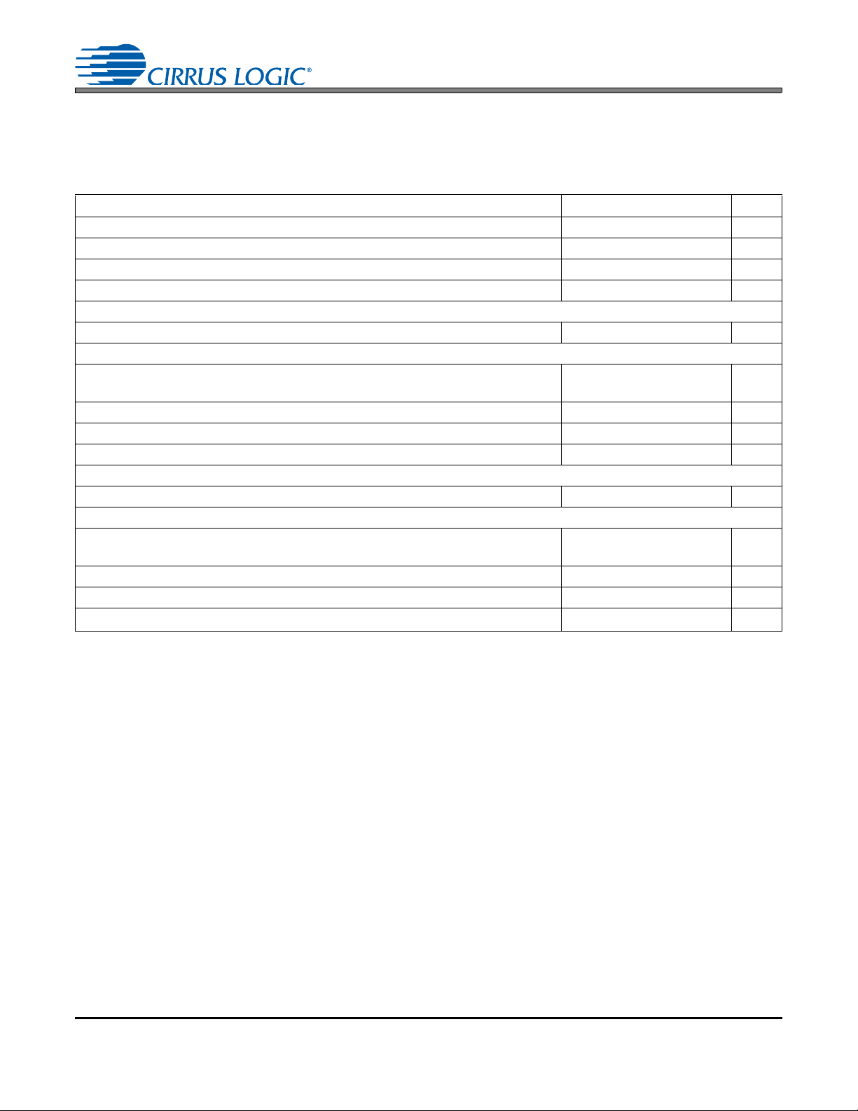
4.6 Internal Signal Path
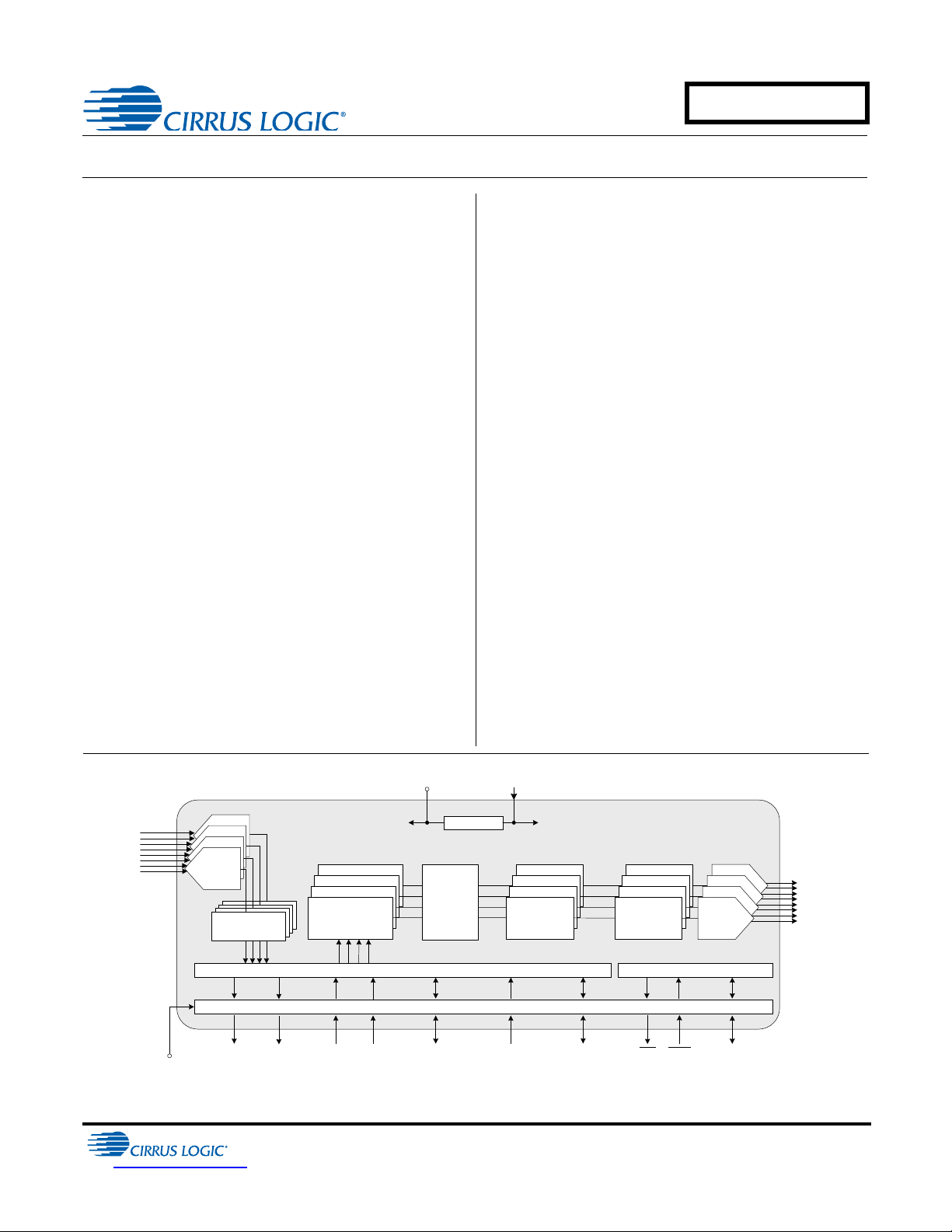
I2C Control
Data
Control Port
Level Tr anslator
VL
1 .8 to 5.0 VDC
RST
INT
SDOU T1
LDO Analog Supply
2.5 V
VA
5.0 VDC
VD
2.5 VDC
Seri al Audi o Interfac e
SDOU T2
Seri al C loc k
In/Out
Master Clock In
Fr ame Sync
Clock / LRCK
SDIN 1SDIN2
AIN4 (± )
AIN3 (± )
AIN2 (± )
AIN1 (± )
Di gital F ilter s
Multi-bit
ADC
AOUT 1 (±)
AOUT 2 (±)
AOUT 3 (±)
AOUT 4 (±)
Inter polati on
Filter
Multi-bit
Modul ators
Channel Volume ,
Mute, Invert ,
Noise Gate
DAC &
Analog
Filters
Master
Volume
Contr ol
Figure 19. Audio Path Routing
The CS4244 device includes two paths in which audio data can be routed. The analog input path, shown in
yellow, allows up to four analog signals to be combined into a single TDM stream on the SDOUT1 pin or
output as stereo pairs on the SDOUT1 and SDOUT2 pins. The DAC1-4 path, highlighted in blue, converts
serial audio data to analog audio data.
CS4244
4.6.1 Routing the Serial Data within the Signal Paths
4.6.1.1 ADC Signal Routing
In TDM mode, the CS4244 is designed to load the first four slots of the TDM stream on the SDOUT1 pin
with the internal ADC data. Additionally, in order to minimize the number of SDOUT lines that must be run
to the system controller in a multiple IC application, the SDOUT data for up to 4 devices can be loaded
into a single TDM stream by side chaining the devices together, as shown in Figure 20. To enable the
sidechain feature, the “SDO CHAIN” bit in the "SP Control" register must be set.
DS900F1 31
Page 32

CS4244
Device D
SDIN 2
SDOU T1
SDIN 1
x
x
Device A
SDIN 2
SDOU T1
SDIN 1
x
x
x
Device B
SDIN 2
SDOU T1
SDIN 1
x
x
x
Device C
SDIN 2
SDOU T1
SDIN 1
x
x
x
DSP
x
ADC data from Device A is loaded into the
first 4 slots of the 16 slot TDM Stream
going out of SDOUT1 pin of Device A. The
last 12 slots are all coded as “0's”.
The ADC data of Device B is coded into the
first four slots of the output TDM stream,
followed by the first 12 slots of the TDM
stream coming in on SDIN2, placing the
ADC data from Device A into slots 5-8 of the
outgoing TDM stream.
The ADC data of Device C is coded into the
first four slots of the output TDM stream,
followed by the first 12 slots of the TDM
stream coming in on SDIN2, placing the
ADC data from Device B into slots 5- 8 and
the ADC data from D evice A into slots 9-12
of the outgoing TDM stream.
The ADC data of Device D is coded into the
first four slots of the output TDM stream,
followed by the first 12 slots of the TDM
stream coming in on SDIN2, placing the
ADC dat a fr om Device C in to sl ots 5- 8, the
ADC data from Device B into slots 9-12, and
the ADC data from Device A into slots 13-16
of the outgoing TDM stream.
Device D
SDIN2
SDOUT1
SDIN1
x
x
Device A
SDIN2
SDOUT1
SDIN1
x
x
x
Device B
SDIN2
SDOUT1
SDIN1
x
x
x
Device C
SDIN2
SDOUT1
SDIN1
x
x
x
DSP
x
Each of the device’s ADC data
is reflected in the TDM stream
on SDOUT1 and then routed to
the system controller.
Note:
This diagram shows the configuration for 16 slot TDM streams. If 8 slot TDM streams are used, two separate serial data lines will need to be
connected from the DSP. One would carry the serial data for Devices C&D and the other would carry the serial data for Devices A&B
Figure 20. Conventional SDOUT (Left) vs. Sidechain SDOUT (Right) Configuration
In Left Justified or I²S mode, the CS4244 transmits the AIN1 and AIN2 signals on the SDOUT1 pin and
the AIN3 and AIN4 signals on the SDOUT2 pin.
4.6.1.2 DAC1-4 Signal Routing
In TDM mode, the “DAC1-4 SOURCE[2:0]” bits in the "SP Data Sel." register advise the CS4244 where
data for the DAC1-4 path is located within the incoming TDM streams. Details for this register and the bit
settings can be found in Figures 21 and 22.
In Left Justified or I²S mode, the CS4244 routes the data on the SDIN1 pin to DAC1 and DAC2 and the
data on the SDIN2 pin to DAC3 and DAC4.
DS900F1 32
Page 33

CS4244
DAC1-4 Source [2:0] DAC1-4 Data is in:
000 Slots 1-4 of SDIN1
001 Slots 5-8 of SDIN1
010
Slots 9-12 of SDIN1
011
Slots 13-16 of SDIN1
100
Slots 1-4 of SDIN2
101
Slots 5-8 of SDIN2
110
Slots 9-12 of SDIN2
111 Slots 13-16 of SDIN2
SDIN1
SDIN2
FS/LRCK = 48/96kHz
MCLK = 12.288/24.576MHz
SCLK = 12.288/24.576MHz
Slot 1 [31:0] Slot 2 [31:0] Slot 3 [31:0] Slot 4 [31:0] Slot 5 [31:0] Slot 6 [31:0] Slot 7 [31:0] Slot 8 [31:0]
Slot 1 [31:0] Slot 2 [31:0] Slot 3 [31:0] Slot 4 [31:0] Slot 5 [31:0] Slot 6 [31:0] Slot 7 [31:0] Slot 8 [31:0]
SDIN1
SDIN2
MCLK = 24.576MHz
FS/LRCK = 48kHz
SCLK = 24.576MHz
…→……→……→…
Slot 8 [31:0] Slot 9 [31:0]
Slot 8 [31:0] Slot 9 [31:0]
Slot 1 [31:0]
Slot 1 [31:0]
Slot 4 [31:0] Slot 5 [31:0]
Slot 4 [31:0] Slot 5 [31:0]
…→…
Slot 13 [31:0]
Slot 12 [31:0] Slot 13 [31:0]
Slot 16 [31:0]
Slot 16 [31:0]
Slot 12 [31:0]
Figure 21. DAC1-4 Serial Data Source Selection
DS900F1 33
Page 34

CS4244
111 Slots 13-16 of SDIN2
101
Slots 5-8 of SDIN2
110
Slots 9-12 of SDIN2
011
Slots 13-16 of SDIN1
100
Slots 1-4 of SDIN2
001 Slots 5-8 of SDIN1
010
Slots 9-12 of SDIN1
DAC1-4 Source [2:0] DAC1-4 Data is in:
000 Slots 1-4 of SDIN1
SDIN1
SDIN2
MCLK = 12.288/24.576MHz
FS/LRCK = 48/96kHz
SCLK = 12.288/24.576MHz
Slot 1 [31:0] Slot 2 [31:0] Slot 3 [31:0] Slot 4 [31:0] Slot 5 [31:0] Slot 6 [31:0] Slot 7 [31:0] Slot 8 [31:0]
DAC1 [23:0] x DAC2 [23:0] x DAC3 [23:0] x DAC4 [23:0] x x x x x
xxxx xxxx
Figure 22. Example Serial Data Source Selection
DS900F1 34
Page 35

4.6.2 ADC Path
I2C C ontrol
Data
Cont rol Port
Level T ranslator
VL
1 .8 to 5.0 VDC
RST
INT
SDOU T1
LDO Analog Supply
2.5 V
VA
5.0 VDC
VD
2.5 VDC
Ser ial Audio Inter face
SDOU T2
Seri al C lock
In/O ut
Master Clock In
Fr ame Sync
Clock / LRCK
SDIN 1SDIN 2
AIN4 (± )
AIN3 (± )
AIN2 (± )
AIN1 (± )
Digital Filters
Multi-bit
ADC
AOUT 1 (±)
AOUT 2 (±)
AOUT 3 (±)
AOUT 4 (±)
Inter polati on
Filter
Multi-bit
Modulators
Channel Volum e ,
Mute , Invert ,
Noise Gate
DAC &
Analog
Filters
Master
Volum e
Cont rol
Figure 23. ADC Path
4.6.2.1 Analog Inputs
CS4244
AINx+ and AINx- are line-level differential analog inputs. The analog input pins do not self-bias and must
be externally biased to VA/2 to avoid clipping of the input signal. The full-scale analog input levels are
scaled according to VA and can be found in the Analog Input Characteristics tables on pages 11 and 12.
The ADC output data is in two’s complement binary format. For inputs above positive full scale or below
negative full scale, the ADC will output 7FFFFFH or 800000H, respectively, and cause the ADC Overflow
bit in the Interrupt Notification 1 register to be set to a ‘1’.
4.6.2.2 Active ADC Input Filter
The analog modulator samples the input at 6.144 MHz (internal MCLK = 12.288 MHz). The digital filter
will reject signals within the stopband of the filter. However, there is no rejection for input signals which
are multiples of the digital passband frequency (n
a recommended analog input filter that will attenuate any noise energy at 6.144 MHz, in addition to providing the optimum source impedance for the modulators. The use of capacitors that have a large voltage
coefficient (such as general-purpose ceramics) must be avoided since these can degrade signal linearity.
6.144 MHz), where n = 0,1,2,... Refer to Figure 24 for
DS900F1 35
Page 36

CS4244
VA
+
+
-
-
22 F
100 k
100 k
100 k
100 k
0.01 F22 F
470 pF
470 pF
C0G
C0G
634
634
634
91
91
2700 pF
C0G
AINx+
AINx-
ADC1-4
* Plac e close to AINx pins
*
Figure 24. Single-Ended to Differential Active Input Filter
VA
+
+
-
-
100 k
100 k
100 k
0.01 F 22 F
470 pF
470 pF
C0G
C0G
634
634
634
91
91
2700 pF
C0G
AINx+
AINx-
ADC1-4
* Plac e close to AINx pins
*
Figure 25. Single-Ended to Differential Active Input Filter - DC Coupled Input Signal (VA/2 Centered)
4.6.2.3 ADC HPF
The ADC path contains an optional HPF which can be enabled or disabled for all four ADCs via the “EN-
ABLE HPF” bit in the "ADC Control 1" register. The HPF should only be disabled when the DC component
of the input signal needs to be preserved in the digital output data. The HPF characteristics are given in
the ADC Digital Filter Characteristics table and plotted in Section 7. The Analog Input Characteristics tables on pages 11 and 12 specify the DC offset error when the HPF is enabled or disabled.
The following figure shows how the recommended single-ended to differential active input filter
(Figure 24) can be modified to allow for DC coupled inputs when the HPF is disabled. Note that the voltage swing should not exceed the ADC full-scale input specification.
DS900F1 36
Page 37

4.6.3 DAC1-4 Path
I2C Control
Data
Contr ol Por t
Level Transl ator
VL
1. 8 to 5.0 VDC
RST
INT
SDOU T1
LDO Analog Supply
2.5 V
VA
5.0 VD C
VD
2.5 VDC
Seri al Audio Inter face
SDOU T2
Seri al Cl ock
In/Out
Mas ter Cl ock In
Fr ame Sync
Clock / LRCK
SDIN 1SD IN2
AOUT 1 (±)
AOUT 2 (±)
AOUT 3 (±)
AOUT 4 (±)
Inter polation
Filter
Multi-bit
Modul ators
Channel Volume ,
Mute , Invert ,
Noise Gate
DAC &
Anal og
Filters
Master
Volume
Contr ol
AIN4 (± )
AIN3 (± )
AIN2 (± )
AIN1 (± )
Digital Filters
Multi-bit
ADC
Figure 26. DAC1-4 Path
The AOUT1-4 signals are driven by the data placed into the DAC1-4 path. This data can be placed into
the DAC1-4 path via the DAC1-4 Data Source settings in the control port. These settings allow the input
source to be selected from any of the up to 32 slots of data on the incoming TDM streams on SDIN1 and
SDIN2.
CS4244
The DAC1-4 path also includes individual channel mutes. Separate volume controls are available for each
channel, along with a master volume control that simultaneously attenuates all four channels. The master
volume attenuation is added to any channel attenuation that is applied.
4.6.3.1 De-emphasis Filter
The CS4244 includes on-chip digital de-emphasis for 32, 44.1, and 48 kHz sample rates. It is not supported for 96 kHz or for any settings in Double-speed Mode. The filter response is adjusted to be appropriate
for a particular base rate by the Base Rate Advisory bits. This filter response, shown in Figure 27, will vary
if these bits are not set appropriately for the given base rate. The frequency response of the de-emphasis
curve scales proportionally with changes in sample rate, F
phasis for de-emphasis control.
The de-emphasis feature is included to accommodate audio recordings that utilize 50/15 s pre-emphasis
equalization as a means of noise reduction.
. Please see Section 6.9.2 DAC1-4 De-em-
S
DS900F1 37
Page 38

De-emphasis is only available in Single-speed Mode.
Gain
dB
-10dB
0dB
Frequency
T2 = 15 µs
T1=50 µs
F1 F2
3.183 kHz 10.61 kHz
Figure 27. De-emphasis Curve
DAC1-4
AOUTx+
22 µF
1500 pF
470
47 k
C0G
AOUTx-
22 µF
1500 pF
470
47 k
C0G
Figure 28. Passive Analog Output Filter
4.6.4 Analog Outputs
The recommended differential passive output filter is shown below. The filter has a flat frequency response in the audio band while rejecting as much signal energy outside of the audio band as possible.
The filter has a single-pole high-pass filter to AC-couple the output signal to the load and a single-pole
low-pass filter to attenuate high-frequency energy resulting from the CS4244 DAC’s noise shaping function.
CS4244
DS900F1 38
Page 39

4.6.5 Volume Control
1
0
Noise Gate
Soft Ramp
0
1
x
DACx Data
+
DACx Volume
Regi ster Set ting
Master Volume
Regi ster S etting
Inter polati on
Filter
Modul ator DAC
Lim iter
(+6 to -90 dB)
INV DACx
DAC1-4 Noise
Gate Threshold
MUTE DACx
DAC1-4 ATT
AOUT x
Figure 29. Volume Implementation for the DAC1-4 Path
The CS4244 includes a volume control for the DAC1-4 signal path. The implementation details for the volume control and other associated peripheries for DAC1-4 is shown in Figure 29 below. Digital volume
steps, adjustable noise gating, muting, and soft ramping are provided on each DAC channel.
4.6.5.1 Mute Behavior
Each DAC channel volume is controlled by the sum (in dB) of the individual channel volume and the master volume registers. The channel and master volume control registers have a range of +6 dB to -90 dB
with a nominal resolution of
volume settings is limited to a range of +6 dB to -90 dB. Any volume setting below this range will result in
infinite attenuation thus muting the channel.
CS4244
6.02
/16dB per each bit, which is approximately 0.4 dB. The sum of the two
A DAC channel may alternatively be muted by using the mute register bits, the power down bits, or the
Noise Gate feature. For any case when the mute engages (volume is less than -90 dB, power down bit is
set, mute bit is set, or Noise Gate is engaged), the CS4244 will mute the channel immediately or soft-ramp
the volume down at a rate specified by the MUTE DELAY[1:0] bits depending on the settings of the DAC1-
4 ATT. bit in the "DAC Control 3" register. This behavior also applies when unmuting a channel.
4.6.5.2 Soft Ramp
The CS4244 soft ramp feature (enabled using the DAC1-4 ATT. bit) is activated on mute and unmute transitions as well as any normal volume register changes. To avoid any potential audible artifacts due to the
soft ramping, the volume control algorithm implements the ramping function differently based upon how
the user attempts to control the volume.
If the user changes the volume in distant discrete steps such as what would happen if a button were
pressed on a user interface to temporarily add attenuation to or mute a channel, then the volume is
ramped from the current setting to the new setting at a constant rate set by the MUTE DELAY[1:0] bits.
Alternatively, if the user controls the volume through a knob or slider interface, a volume envelope is sampled at a slow, not-necessarily uniform rate (typically 1-20 Hz) and sent to the CS4244. In this case the
ramping algorithm detects a short succession of volume changes attempting to track the volume envelope
and dynamically adjusts the soft-ramp rate.
If the CS4244 were to use a constant ramp rate between the volume changes it receives, its output volume
envelope may either lag behind the user-generated envelope if the ramp rate is set too low (possibly not
reaching the peaks and dulling the envelope) or the output volume envelope may cause a stair-case effect
resulting in audible zipper noise if the ramp rate is set too high. By instead adapting the soft-ramp rate to
fit the envelope given by the incoming volume samples, the envelope lag time is limited and the zipper
DS900F1 39
Page 40

CS4244
USER: Change
Vol ume or Mute
Register
Wait State
Envelope Counter
Running
Envelope
Counter
Timed Out?
Yes
No
Reset Envelope
Counter
Limi t Ramp Rate
Reset Envelope
Counter
Ramp R ate =
MUTE_DELAY
Changes VolumeBetween Time
Setting Vo lumeCu rrent - Setting Volume New
Rate Ramp
MIN_DELAY
MAX_DELAY
Figure 30. Soft Ramp Behavior
noise is avoided. In this mode the soft ramp algorithm linearly interpolates the volume between the volume
changes. There is a lag of one volume change sample since two samples are required to calculate the
first ramp rate.
See Figure 30 for the soft ramp diagram. On the first volume sample received, the CS4244 only detects
the possible beginning of a volume envelope sequence and resets an envelope counter. The volume
starts ramping to the new volume setting at a constant rate controlled by the MUTE DELAY[1:0] setting.
If the envelope counter times out before a new volume sample is received, the next received sample is
treated in the same way as the previous sample and the ramp rate is kept constant. In this way, as long
as the volume samples are distant from each other by more than the envelope counter time out, the rate
is kept constant resulting in the soft-ramp behavior described in the button-press example.
However if the next volume sample is received before the envelope counter times out, then it is assumed
to be part of a volume envelope sequence. The envelope counter is reset and as long as new samples
are received in succession before a time out occurs, the sequence is continued. Starting at the second
volume sample of an envelope sequence, the ramp rate is adjusted using the equation shown in
Figure 30.
Two control parameters allow the user to limit the ramp-rate range to achieve optimum effect. The MIN
DELAY[2:0] setting limits the maximum ramp rate; higher values will introduce more lag in the envelope
tracking while providing a smoother ramp. The MAX DELAY[2:0] setting limits the minimum ramp rate;
ues of these registers are recommended as a starting point. It is possible to disable the volume envelope
lower values will permit closer tracking of the envelope but may re-introduce zipper noise. The default val-
DS900F1 40
Page 41

CS4244
tracking and always produce a constant ramp rate. To accomplish this, set the MIN DELAY[2:0] and MAX
DELAY[2:0] values to match the MUTE DELAY[1:0] setting.
The envelope counter time out period which defines the boundary between the two soft-ramping behaviors depends on the base rate. It is equal to approximately 100,000/Fs.
The MUTE DELAY[1:0], MIN DELAY[2:0], and MAX DELAY[2:0] bits specify a delay equal to a multiple
of the base period between volume steps of
6.02
/64dB, which is approximately 0.1 dB. This is the internal
resolution of the volume control engine. Consequently the soft-ramp rate can be expressed in ms/dB as
shown in Table 6.
Fs = 48 kHz or 96 kHz (Base = 48 kHz) Fs = 32 kHz or 64 kHz (Base = 32 kHz)
Time to Ramp
Ramp Rate
1 x Base 21.33 1.33 0.22 32 2 0.33
2 x Base 42.67 2.67 0.44 64 4 0.66
4 x Base 85.33 5.33 0.89 128 8 1.33
8 x Base 170.67 10.67 1.77 256 16 2.66
16 x Base 341.33 21.33 3.54 512 32 5.32
32 x Base 682.67 42.67 7.09 1024 64 10.63
64 x Base 1365.33 85.33 14.17 2048 128 21.26
128 x Base 2730.67 170.67 28.35 4096 256 42.52
to Full Scale
(ms)
Time to Ramp
6 dB (ms)
ms/dB
Time to Ramp
to Full Scale
(ms)
Time to Ramp
6 dB (ms)
ms/dB
Table 6. Soft Ramp Rates
Full-scale ramp is 96 dB (-90 dB to +6 dB)
4.6.5.3 Noise Gate
The CS4244 is equipped with a Noise Gate feature that mutes the output if the signal drops below a given
bit depth for 8192 samples. While the enabling or disabling of the Noise Gate feature is done for the entire
DAC1-4 output path, each of the channels within the path have separate monitoring circuitry that will trigger the Noise Gate function independently of the other channels. For instance, if the Noise Gate were enabled for and one of the channels were to exhibit a pattern of more than 8192 samples of either all “1’s”
or all “0’s”, the output for that particular channel would be muted (and subsequently unmuted), independently of the other channels. To enable the Noise Gate feature, set the DAC1-4 NG[2:0] bits to the desired
bit depth. The available bit depth settings are shown in Table 7.
DAC1-4 NG[2:0] Setting Channel is muted after “x” bits
000 Upper 13 Bits (-72 dB)
001 Upper 14 Bits (-78 dB)
010 Upper 15 Bits (-82 dB)
011 Upper 16 Bits (-90 dB)
100 Upper 17 Bits (-94 dB)
101 Upper 18 Bits (-102 dB)
110 Upper 24 Bits (-138 dB)
111 Noise Gate Disabled
Table 7. Noise Gate Bit Depth Settings
DS900F1 41
Page 42

When the upper “x” bits, as dictated by the DAC1-4 NG[2:0] settings, are either all “1’s” or all “0’s” for 8192
consecutive samples, the Noise Gate will engage for that channel. Setting these bits to ‘111’ will disable
the Noise Gate feature. If the Noise Gate feature engages, it will transition into and out of mute as dictated
by the DAC1-4 ATT. bit in the "DAC Control 3" register.
4.7 Reset Line
The reset line of the CS4244 is used to place the device into a reset condition. In this condition, all of the
values of the CS4244 control port are set to their default values. This mode of operation is the lowest power
mode of operation for the CS4244 and should be used whenever the device is not operating in order to save
power. During the power up and power down sequence, it is often necessary for the CS4244 devices to be
placed into (and taken out of) reset at a different moment in time than the amplifiers to which they are connected in order to minimize audible clicks and pops during the sequence. For this reason, it is advisable to
run separate reset lines for each type of device, i.e. one reset line for the CS4244 devices and one for the
amplifier devices.
4.8 Error Reporting and Interrupt Behavior
The CS4244 is equipped with a suite of error reporting and protection. The types of errors that are detected,
the notification method for these errors, and the steps needed to clear the errors are detailed in Table 8.
It is important to note that the interrupt notification bits for all of the errors are triggered on the edge of the
occurrence of the event. They are not level-triggered and therefore do not indicate the presence of an error
in real time. This means that, a “1” in the error’s respective field inside the Interrupt Notification register only
indicates that the error has occurred since the last time the register was cleared and not necessarily that
the error is currently occurring.
CS4244
Note:
All PDNx bits must be set
Event(s) that
Name of Error
Disallowed Test Mode
Entry
(Note 35)
Serial Port Error FS/LRCK, or SCLK has
Clocking Error The speed mode which the
ADCx Overflow ADC inputs are larger than
DACx Clip DAC output level is larger
Caused the Error
Device has entered test
mode due to an errant I²C
write.
become invalid.
device is receiving is different
than the speed mode set in
the SPEED MODE bits, or
the PLL is unlocked from
input signal.
the permitted full scale signal.
than the available rail voltage.
Outputs Muted
Upon Occurrence?
No No
Yes Yes
Yes Yes
No No
No No
and then cleared to
resume normal operation?
(Normal operation will continue
but audible distortion will occur.)
Normal operation will continue
but audible distortion will occur.
Table 8. Error Reporting and Interrupt Behavior Details
35. This error is provided to aid in trouble shooting during software development. Entry into the test mode
of the device may cause permanent damage to the device and should not be done intentionally.
DS900F1 42
Page 43

4.8.1 Interrupt Masking
An occurrence of any of the errors mentioned above will cause the interrupt line to engage in order to notify the system controller that an error has occurred. If it is preferred that the error not cause the interrupt
line to engage, this error can be masked in its respective mask register. It is important to note that, in the
event of an error, the interrupt notification bit for the respective error will reflect the occurrence of the
event, regardless of the setting of the mask bit. Setting the mask bit only prevents the interrupt pin from
being flagged upon the occurrence.
4.8.2 Interrupt Line Operation
As mentioned previously, the interrupt line of the CS4244 will be pulled low or high (depending on the settings of the “INT PIN[1:0]” bits in the "Interrupt Control" register) after an interrupt condition occurs, pro-
vided that the event is not masked in the mask register. If the CS4244’s interrupt line is to be connected
onto a single bus with other devices, it is advisable to use it in the open drain mode of operation. If no
other devices are connected to the interrupt line, it may be used in the CMOS mode of operation. When
used in the open drain configuration, it is necessary to connect a pull-up resistor to this net, which will
ensure a known state on the net when no error is present. Please refer to the typical connection diagram
for the appropriate pull-up resistor value.
4.8.3 Error Reporting and Clearing
In the event of an error, the interrupt line will be engaged - provided the mask bit for that error is not set.
When the interrupt notification registers are read to determine the source of the error, the mask bit for
whichever error occurred will be set automatically by the CS4244. The system controller should begin to
take corrective action to clear the error. Once the error has been cleared, the system controller should
clear the mask bit in the appropriate mask register to ensure that a subsequent occurrence of the error
will cause the interrupt line to engage appropriately. This behavior is detailed in Figure 31 on page 44.
CS4244
DS900F1 43
Page 44

USER: Mask bit(s)
set to 0
Unmasked error
occurs
Status Register bit
changes to ‘1’ and
INT pin set to
active level
USER: Read
Status Registers
(see status bit(s) =
‘1’)
Mask bit(s) of
corresponding
status bit(s) set to
‘1’
Are any
errors still
occurring?
Yes
No
Status Register
bit(s) set to ‘ 1’
USER: Read
Status Registers
(see all status bits
= ‘0’)
All Status Register
bits cleared
INT pin set to
inactive level
USER: Takes
Corrective Action
New Unmasked Error
New Unmasked Error
New Unmasked Error
New Unmasked Error
New Unmasked Error
New Unmasked Error
Figure 31. Interrupt Behavior and Example Interrupt Service Routine
CS4244
DS900F1 44
Page 45

CS4244
5. REGISTER QUICK REFERENCE
Default values are shown below the bit names.
AD Function 7 6 5 4 3 2 1 0
(Read Only Bits are shown in Italics)
01h
p47
02h
p47
03h
p47
04h
05h
p47
06h
p48
07h
p49
08h
p49
09h
p50
0Ah
0Bh
0Ch
0Dh
0Eh
0Fh
p51
10h
p51
11h
12h
p52
13h
p52
14h
p53
15h
p53
Device ID
A & B
Device ID
C & D
Device ID
E & F
Variant ID
Revision ID
Clock &
SP Sel.
Sample
Width Sel.
SP Control
SP Data
Sel.
Reserved
Reserved
Reserved
Reserved
Reserved
ADC
Control 1
ADC
Control 2
Reserved
DAC
Control 1
DAC
Control 2
DAC
Control 3
DAC
Control 4
0 1 0 0 0 0 1 0
0 0 1 1 0 1 0 0
0 0 0 0 0 0 0 0
0 0 0 0 0 0 0 0
xx x x xxxx
BASE RATE[1:0] SPEED MODE[1:0] MCLK RATE[2:0] Reserved
0 0 0 0 0 1 0 0
SDOUTx SW[1:0] INPUT SW[1:0] Reserved[1:0] Reserved[1:0]
1 1 1 1 1 1 1 1
INV SCLK Reserved[2:0] SP FORMAT[1:0] SDO CHAIN
0 1 0 0 1 0 0 0
Reserved Reserved DAC1-4 SOURCE[2:0] Reserved[2:0]
0 0 0 0 0 0 0 1
1 1 1 1 1 1 1 1
1 1 1 1 1 1 1 1
1 1 1 1 1 1 1 1
1 1 1 1 1 1 1 1
Reserved Reserved[2:0] Reserved[3:0]
0 0 0 0 0 0 0 0
Reserved Reserved VA_SEL
1 1 0 0 0 0 0 0
MUTE
ADC4
1 1 1 1 1 1 1 1
1 1 1 0 0 0 0 0
DAC1-4 NG[2:0] DAC1-4 DE Reserved Reserved Reserved
1 1 1 0 0 0 0 0
1 1 1 0 0 0 0 0
Reserved
1 0 1 1 1 1 1 1
VQ RAMP Reserved[1:0] Reserved PDN DAC4 PDN DAC3 PDN DAC2 PDN DAC1
0 0 0 1 1 1 1 1
DEV. ID A[3:0] DEV. ID B[3:0]
DEV. ID C[3:0] DEV. ID D[3:0]
DEV. ID E[3:0] DEV. ID F[3:0]
Reserved [3:0] Reserved [3:0]
ALPHA REV. ID[3:0] NUMERIC REV. ID[3:0]
MSTR/SLV
Reserved[7:0]
Reserved[7:0]
Reserved[7:0]
Reserved[7:0]
ENABLE
HPF
MUTE
ADC3
Reserved[2:0] Reserved Reserved Reserved Reserved Reserved
Reserved[2:0] Reserved INV. DAC4 INV. DAC3 INV. DAC2 INV. DAC1
DAC1-4
ATT.
MUTE
ADC2
Reserved Reserved MUTE DAC4 MUTE DAC3 MUTE DAC2 MUTE DAC1
MUTE
ADC1
INV. ADC4 INV. ADC3 INV. ADC2 INV. ADC1
PDN
ADC4
PDN
ADC3
PDN
ADC2
PDN
ADC1
DS900F1 45
Page 46

CS4244
AD Function 7 6 5 4 3 2 1 0
(Read Only Bits are shown in Italics)
16h
p54
17h
p55
18h
p55
19h
p55
1Ah
p55
1Bh
p55
1Ch
1Dh
1Eh
p55
1Fh
p56
20h
p57
21h
p57
22h
p58
Volume
Mode
Master
Volume
DAC1
Volume
DAC2
Volume
DAC3
Volume
DAC4
Volume
Reserved
Reserved
Interrupt
Control
Interrupt
Mask 1
Interrupt
Mask 2
Interrupt
Notification 1
Interrupt
Notification 2
MUTE DELAY[1:0] MIN DELAY[2:0] MAX DELAY[2:0]
1 0 0 0 0 1 1 1
MASTER VOLUME[7:0]
0 0 0 1 0 0 0 0
DAC1 VOLUME[7:0]
0 0 0 1 0 0 0 0
DAC2 VOLUME[7:0]
0 0 0 1 0 0 0 0
DAC3 VOLUME[7:0]
0 0 0 1 0 0 0 0
DAC4 VOLUME[7:0]
0 0 0 1 0 0 0 0
Reserved[7:0]
0 0 0 1 0 0 0 0
Reserved[3:0] Reserved[3:0]
1 0 1 1 1 0 1 0
INT MODE INT PIN[1:0] Reserved Reserved Reserved Reserved Reserved
0 1 0 0 0 0 0 0
MASK
TST MODE
ERR
0 0 0 1 0 0 0 0
Reserved Reserved Reserved Reserved
0 0 1 0 0 0 0 0
TST MODE SP ERR CLK ERR Reserved ADC4 OVFL ADC3 OVFL ADC2 OVFL ADC1 OVFL
x x x x x x x x
Reserved Reserved Reserved Reserved DAC4 CLIP DAC3 CLIP DAC2 CLIP DAC1 CLIP
x x x x x x x x
MASK
SP ERR
MASK
CLK ERR
Reserved
MASK
ADC4 OVFL
MASK
DAC4 CLIP
MASK
ADC3 OVFL
MASK
DAC3 CLIP
MASK
ADC2 OVFL
MASK
DAC2 CLIP
MASK
ADC1 OVFL
MASK
DAC1 CLIP
DS900F1 46
Page 47

CS4244
6. REGISTER DESCRIPTIONS
All registers are read/write unless otherwise stated. All “Reserved” bits must maintain their default state. Default
values are shaded.
6.1 Device I.D. A–F (Address 01h–03h) (Read Only)
76543210
DEV. ID A[3:0] DEV. ID B[3:0]
76543210
DEV. ID C[3:0] DEV. ID D[3:0]
76543210
DEV. ID E[3:0] DEV. ID F[3:0]
6.1.1 Device I.D. (Read Only)
Device I.D. code for the CS4244. Example:.
DEV. ID A[3:0] DEV. ID B[3:0] DEV. ID C[3:0] DEV. ID D[3:0] DEV. ID E[3:0] DEV. ID F[3:0] Part Number
4h 2h 3h 4h 0h 0h CS4244
6.2 Revision I.D. (Address 05h) (Read Only)
76543210
AREVID3 AREVID2 AREVID1 AREVID0 NREVID3 NREVID2 NREVID1 NREVID0
6.2.1 Alpha Revision (Read Only)
CS4244 Alpha (silicon) revision level.
AREVID[3:0] Alpha Revision Level
Ah A
... ...
6.2.2 Numeric Revision (Read Only)
CS4244 Numeric (metal) revision level.
NREVID[3:0] Numeric Revision Level
0h 0
... ...
Note: The Alpha and Numeric revision I.D. are used to form the complete device revision I.D. Example:
A0, A1, B0, B1, B2, etc.
DS900F1 47
Page 48

CS4244
6.3 Clock & SP Select (Address 06h)
76543210
BASE RATE[1:0] SPEED MODE[1:0] MCLK RATE[2:0] Reserved
6.3.1 Base Rate Advisory
Advises the CS4244 of the base rate of the incoming base rate. This allows for the de-emphasis filters to
be adjusted appropriately. The CS4244 includes on-chip digital de-emphasis for 32, 44.1, and 48 kHz
base rates. It is not supported for 96 kHz or for any settings in Double Speed Mode.
BASE RATE Base Rate is:
00 48 kHz
01 44.1 kHz
10 32 kHz
11 Re serv ed
6.3.2 Speed Mode
Sets the speed mode in which the CS4244 will operate..
SPEED MODE Speed Mode is:
00 Single Speed Mode
01 Double Speed Mode
10 Reserved
11 Auto Detect (Slave Mode only)
6.3.3 Master Clock Rate
Sets the rate at which the master clock is entering the CS4244. Settings are given in “x” multiplied by the
incoming sample rate, as MCLK must scale directly with incoming sample rate.
MCLK RATE MCLK is:
000
001 384xF
010 512xFS in Single Speed Mode or 256xFS in Double Speed Modex
011 Reserved
100 Reserved
101 Reserved
110 Reserved
111 Reserved
256xF
S
S
in Single Speed Mode or 128xFS in Double Speed Mode
in Single Speed Mode or 192xFS in Double Speed Mode
DS900F1 48
Page 49

CS4244
6.4 Sample Width Select (Address 07h)
76543210
SDOUTx SW[1:0] INPUT SW[1:0] Reserved[1:0] Reserved[1:0]
6.4.1 Output Sample Width
These bits set the width of the samples placed into the outgoing SDOUTx streams.
OUTPUT SW Sample Width is:
00 16 bits
01 18 bits
10 20 bits
11 24 bits
Note: Bits wider than the Output Sample Width setting are cleared within the SDOUTx data stream.
6.4.2 Input Sample Width
These bits set the width of the samples coming into the CS4244 through the SDINx TDM streams.
INPUT SW Sample Width is:
00 16 bits
01 18 bits
10 20 bits
11 24 bits
Note: In Left Justified or I²S mode, the Input Sample Width is fixed to 24 bits.
6.5 Serial Port Control (Address 08h)
76543210
INV SCLK Reserved[2:0] SP FORMAT[1:0] SDO CHAIN MASTER/
SLAVE
6.5.1 Invert SCLK
When set, this bit inverts the polarity of the SCLK signal.
INV SCLK SCLK is:
0 Not Inverted
1 Inverted
6.5.2 Serial Port Format
Sets the format of both the incoming serial data signals and outgoing serial data signals.
SP FORMAT Format is:
00 Left Justified
01 I²S
10 TDM (Slave Mode Only)
11 Re serv ed
DS900F1 49
Page 50

CS4244
6.5.3 Serial Data Output Sidechain
Setting this bit enables the SDOUT1 side chain feature. In this mode, the samples from multiple devices
can be coded into one TDM stream. See Section 4.6.2 ADC Path for details.
SDO CHAIN Sidechain is:
0 Disabled
1 Enabled
6.5.4 Master/Slave
Setting this bit places the CS4244 in master mode, clearing it places it in slave mode.
MASTER/SLAVE CS4244 is in:
0 Slave Mode
1Master Mode
Note: I²S and Left Justified are the only serial port formats available if the CS4244 is in Master Mode.
6.6 Serial Port Data Select (Address 09h)
76543210
Reserved Reserved DAC1-4 SOURCE[2:0] Reserved[2:0]
6.6.1 DAC1-4 Data Source
Sets which portion of data is to be routed to the DAC1-4 data paths.
DAC1-4 SOURCE Data is routed into the DAC1-4 path from:
000 Slots 1-4 of the TDM stream on SDIN1
001 Slots 5-8 of the TDM stream on SDIN1
010 Slots 9-12 of the TDM stream on SDIN1
011 Slots 13-16 of the TDM stream on SDIN1
100 Slots 1-4 of the TDM stream on SDIN2
101 Slots 5-8 of the TDM stream on SDIN2
110 Slots 9-12 of the TDM stream on SDIN2
111 Slots 13-16 of the TDM stream on SDIN2
DS900F1 50
Page 51

CS4244
6.7 ADC Control 1 (Address 0Fh)
76543210
Reserved Reserved VA_SEL ENABLE HPF INV. ADC4 INV. ADC3 INV. ADC2 INV. ADC1
6.7.1 VA Sele ct
Scales internal operational voltages appropriately for VA level. Configuring this bit appropriately for the
VA voltage level used in the application is imperative to ensure proper operation of the device.
VA_SEL Must be set when VA is:
0 3.3 VDC
15VDC
6.7.2 Enable High-pass Filter
Enables high-pass filter for the ADC path.
ENABLE HPF High Pass Filter is:
0 Disabled
1 Enabled
6.7.3 Inv. ADCx
Inverts the polarity of the ADCx signal.
INV. ADCx ADCx Polarity is:
0 Not Inverted
1 Inverted
6.8 ADC Control 2 (Address 10h)
76543210
MUTE ADC4 MUTE ADC3 MUTE_ADC2 MUTE ADC1 PDN ADC4 PDN ADC3 PDN ADC2 PDN ADC1
6.8.1 Mute ADCx
Mutes the ADCx signal
MUTE ADCx ADC is:
0 Not Muted
1 Muted
6.8.2 Power Down ADCx
Powers down the ADCx path.
PDN ADCx ADC is:
0 Powered Up
1 Powered Down
DS900F1 51
Page 52

CS4244
6.9 DAC Control 1 (Address 12h)
76543210
DAC1-4 NG DAC1-4 DE Reserved Reserved Reserved
6.9.1 DAC1-4 Noise Gate
This sets the bit depth at which the Noise Gate feature should engage for the DAC1-4 path.
DAC1-4 NG[2:0] Noise Gate is set at: [b]
000
001
010
011
100
101
110
111
6.9.2 DAC1-4 De-emphasis
Enables or disables de-emphasis for the DAC1-4 path. See Section 4.6.3.1 for details. The CS4244 includes on-chip digital de-emphasis for 32, 44.1, and 48 kHz base rates. It is not supported for 96 kHz or
for any settings in Double-speed Mode.
DAC1-4 DE De-emphasis is:
0 Disabled
1 Enabled
Upper 13 Bits (72 dB)
Upper 14 Bits (78 dB)
Upper 15 Bits (84 dB)
Upper 16 Bits (90 dB)
Upper 17 Bits (96 dB)
Upper 18 Bits (102 dB)
Upper 24 Bits (138 dB)
Noise Gate Disabled
6.10 DAC Control 2 (Address 13h)
76543210
Reserved[2:0] Reserved INV. DAC4 INV. DAC3 INV. DAC2 INV. DAC1
6.10.1 Inv. DACx
Inverts the polarity of the DACx signal.
INV. DACx DACx Polarity is:
0 Not Inverted
1 Inverted
DS900F1 52
Page 53

CS4244
6.11 DAC Control 3 (Address 14h)
76543210
Reserved DAC1-4 ATT Reserved Reserved MUTE DAC4 MUTE DAC3 MUTE DAC2 MUTE DAC1
6.11.1 DAC1-4 Attenuation
Sets the mode of attenuation used for the DAC1-4 path.
DAC1-4 ATT Attenuation events happen:
0 On a soft ramp
1 Immediately
Note: Please see Section 4.6.5 Volume Control for more details regarding the attenuation modes.
6.11.2 Mute DACx
Mutes the DACx signal.
MUTE DACx DACx is:
0 Not Muted
1 Muted
6.12 DAC Control 4 (Address 15h)
76543210
VQ RAMP Reserved[1:0] Reserved PDN DAC4 PDN DAC3 PDN DAC2 PDN DAC1
6.12.1 VQ Ramp
Ramps common mode voltage “VQ” down to ground. This bit needs to be set before asserting reset pin.
VQ RAMP Effect:
0 VQ is set at nominal level (VA/2)
1 VQ is ramped from nominal level to ground.
6.12.2 Power Down DACx
Powers down the DACx path.
PDN DACx DACx is:
0 Powered Up
1 Powered Down
DS900F1 53
Page 54

CS4244
6.13 Volume Mode (Address 16h)
76543210
MUTE DELAY[1:0] MIN DELAY[2:0] MAX DELAY[2:0]
6.13.1 Mute Delay
Sets the delay between the volume steps during muting and unmuting of a signal when attenuation mode
is set to soft ramp. Each step of the ramp is equal to
times the base period.
MUTE DELAY Delay is:
00 1x
01 4x
10 16x
11 64x
6.13.2 Minimum Delay
Sets the minimum delay before each volume transition. Settings are given in “x” times the base period.
See Section 4.6.5 Volume Control for more details regarding the operation of the volume control.
MIN DELAY Minimum Delay is:
000 1x
001 2x
010 4x
011 8x
100 16x
101 32x
110 64x
111 128x
6.02
/64dB ~= 0.094 dB. Settings are given as “x”
6.13.3 Maximum Delay
Sets the maximum delay before the volume transition. Settings are given in “x” times the base period. See
Section 4.6.5 Volume Control for more details regarding the operation of the volume control.
MAX DELAY Maximum Delay is:
000 1x
001 2x
010 4x
011 8x
100 16x
101 32x
110 64x
111 128x
DS900F1 54
Page 55

CS4244
6.14 Master and DAC1-4 Volume Control (Address 17h, 18h, 19h, 1Ah, & 1Bh)
76543210
x VOLUME[7:0]
6.14.1 x Volume Control
Sets the level of the x Volume Control. Each volume step equals
4.6.5.1 on page 39 for the muting behavior of these volume registers.
x VOLUME x Volume is: [dB]
00000000 +6.02
00001111 +0.38
00010000 0
00010001 -0.38
00011000 -3.01
... ...
11111110 -89.55 (most total attenuation before mute)
11111111 -89.92 (least total attenuation before unmute)
6.15 Interrupt Control (Address 1Eh)
76543210
INT MODE INT POL [1:0] Reserved Reserved Reserved Reserved Reserved
6.02
/16dB ~= 0.38 dB. See Section
6.15.1 INT MODE
Sets the behavior mode of the interrupt registers of the device. In the default configuration, if the interrupt
notification registers are read and any error is found to have occurred since the last clearing of that register, the device will automatically set the corresponding mask bit in the appropriate mask register. In the
nondefault configuration, mask bits are not set automatically.
INT MODE Upon the reading of an error out of the interrupt notification bits, the CS4244 will:
0 Automatically set the corresponding mask bit.
1 Not set the corresponding mask bit.
6.15.2 Interrupt Pin Polarity
Sets the output mode of the interrupt pin.
INT POL Output mode of the interrupt pin is:
00 Active High
01 Active Low
10 Active Low/Open Drain
11 Re serv ed
DS900F1 55
Page 56

6.16 Interrupt Mask 1 (Address 1Fh)
76543210
MASK
TST MODE ERR
MASK
SP ERR
MASK CLK ERR
Reserved
6.16.1 Test Mode Error Interrupt Mask
Controls whether a Test Mode Error event flags the interrupt pin. A test mode error occurs when an inadvertent I²C write places the device in test mode.
MASKTSTMOD ERR In the event of a Test Mode Error event, Interrupt Pin will:
0 Be Flagged
1 Not be flagged
6.16.2 Serial Port Error Interrupt Mask
Controls whether the interrupt pin if flagged when any of the following parameters are changed without
first powering down the device (i.e., setting all Power Down ADCx and Power Down DACx bits):
• Serial Port Format: SP FORMAT[1:0]
• Speed Mode: SPEED MODE (In slave mode, changing the MCLK/F
device, flags this error and the Clocking Error. In master mode, changing MCLK frequency without the
device being powered down does not flag this or the Clocking Error since MCLK/F
• Master/Slave: MSTR/SLV
MASK
ADC4 OVFL
MASK
ADC3 OVFL
CS4244
MASK
ADC2 OVFL
ratio without powering down the
S
does not change.)
S
MASK
ADC1 OVFL
MASK SP ERR In the event of a Serial Port Error event, Interrupt Pin will:
0 Be Flagged
1 Not be flagged
6.16.3 Clocking Error Interrupt Mask
Allows or prevents a Clocking Error event from flagging the interrupt pin. See Section 4.8 for details.
MASK CLK ERR In the event of a Clocking Error event, Interrupt Pin will:
0 Be Flagged
1 Not be flagged
6.16.4 ADCx Overflow Interrupt Mask
Allows or prevents an ADCx Overflow event from flagging the interrupt pin.
MASK ADCx OVFL In the event of an ADCx Overflow event, Interrupt Pin will:
0 Be Flagged
1 Not be flagged
DS900F1 56
Page 57

CS4244
6.17 Interrupt Mask 2 (Address 20h)
76543210
Reserved Reserved Reserved Reserved
MASK DAC4
CLIP
6.17.1 DACx Clip Interrupt Mask
Allows or prevents a DACx Clip event from flagging the interrupt pin.
MASK DACx CLIP In the event of a DACx Clip event, Interrupt Pin will:
0 Be Flagged
1 Not be flagged
6.18 Interrupt Notification 1 (Address 21h) (Read Only)
76543210
TST MODE ERR SP ERR CLK ERR Reserved ADC4 OVFL ADC3 OVFL ADC2 OVFL ADC1 OVFL
6.18.1 Test Mode Error
A Test Mode Error has occurred since the last clearing of the Interrupt Notification register.
TSTMOD ERR Since the last clearing of the Interrupt Notification Register, a Test Mode Error:
0 Has Not Occurred
1 Has Occurred
MASK DAC3
CLIP
MASK DAC2
CLIP
MASK DAC1
CLIP
6.18.2 Serial Port Error
A Serial Port Error has occurred since the last clearing of the Interrupt Notification register.
SP ERR Since the last clearing of the Interrupt Notification Register, a Serial Port Error:
0 Has Not Occurred
1 Has Occurred
6.18.3 Clocking Error
A Clocking Error has occurred since the last clearing of the Interrupt Notification register.
CLK ERR Since the last clearing of the Interrupt Notification Register, a Clocking Error:
0 Has Not Occurred
1 Has Occurred
6.18.4 ADCx Overflow
An ADCx Overflow has occurred since the last clearing of the Interrupt Notification register.
ADCx OVFL Since the last clearing of the Interrupt Notification Register, a ADCx Overflow Error:
0 Has Not Occurred
1 Has Occurred
DS900F1 57
Page 58

CS4244
6.19 Interrupt Notification 2 (Address 22h) (Read Only)
76543210
Reserved Reserved Reserved Reserved DAC4 CLIP DAC3 CLIP DAC2 CLIP DAC1 CLIP
6.19.1 DACx Clip
A DACx Clip has occurred since the last clearing of the Interrupt Notification register.
DACx CLIP Since the last clearing of the Interrupt Notification Register, a DACx Clip Error:
0 Has Not Occurred
1 Has Occurred
DS900F1 58
Page 59

7. ADC FILTER PLOTS
0 0.1 0.2 0.3 0.4 0.5 0.6 0.7 0.8 0.9 1
−100
−90
−80
−70
−60
−50
−40
−30
−20
−10
0
Frequency (normalized to Fs)
Amplitude (dB)
Stopband Rejection
0.4 0.42 0.44 0.46 0.48 0.5 0.52 0.54 0.56 0.58
−100
−90
−80
−70
−60
−50
−40
−30
−20
−10
0
Frequency (normalized to Fs)
Amplitude (dB)
Transition Band
0.6
Figure 32. ADC Stopband Rejection Figure 33. ADC Transition Band
0.45 0.46 0.47 0.48 0.49 0.5 0.51 0.52 0.53 0.54 0.55
−10
−9
−8
−7
−6
−5
−4
−3
−2
−1
0
Frequency (normalized to Fs)
Amplitude (dB)
Transition Band (Detail)
0 0.05 0.1 0.15 0.2 0.25 0.3 0.35 0.4 0.45 0.5
−0.05
−0.04
−0.03
−0.02
−0.01
0
0.01
0.02
0.03
0.04
0.05
Frequency (normalized to Fs)
Amplitude (dB)
Passband Ripple
Figure 34. ADC Transition Band (Detail)
Figure 35. ADC Passband Ripple
0 2 4 6 8 10 12 14 16 18 20
−3
−2.5
−2
−1.5
−1
−0.5
0
Frequency (Hz)
Amplitude (dB)
High−Pass Filter Response (Fs = 48kHz)
0 2 4 6 8 10 12 14 16 18 20
−3
−2.5
−2
−1.5
−1
−0.5
0
Frequency (Hz)
Amplitude (dB)
High−Pass Filter Response (Fs = 96kHz)
Figure 36. ADC HPF (48 kHz)
Figure 37. ADC HPF (96 kHz)
CS4244
DS900F1 59
Page 60
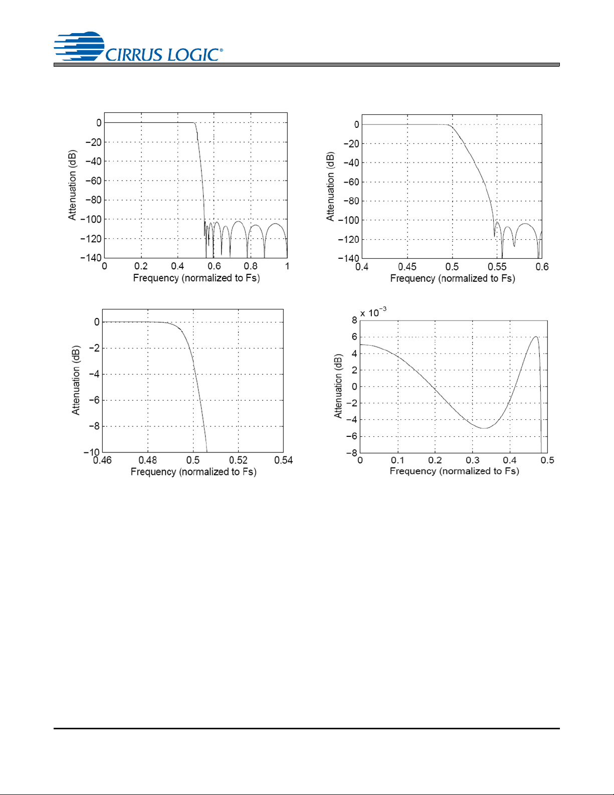
8. DAC FILTER PLOTS
Figure 38. SSM DAC Stopband Rejection Figure 39. SSM DAC Transition Band
Figure 40. SSM DAC Transition Band (Detail)
Figure 41. SSM DAC Passband Ripple
CS4244
DS900F1 60
Page 61

CS4244
Figure 42. DSM DAC Stopband Rejection Figure 43. DSM DAC Transition Band
Figure 44. DSM DAC Transition Band (Detail)
Figure 45. DSM DAC Passband Ripple
DS900F1 61
Page 62

9. PACKAGE DIMENSIONS
eb
A
A1
PIN #1 IDENTIFIER
0.500.10
LASER MARK IN G
E
2.00 REF
D2
L
PIN #1 CORNER
2.00 REF
E2
D
40L QFN (6 6 MM BODY) PACKAGE DRAWING
CS4244
Figure 46. Package Drawing
INCHES MILLIMETERS NOTE
DIM MIN NOM MAX MIN NOM MAX
A -- -- 0.0394 -- -- 1.00 1
A1 0.0000 -- 0.0020 0.00 -- 0.05 1
b .0071 .0091 .0110 0.18 0.23 0.28 1,2
D .2362 BSC 6.00 BSC 1
D2 .1594 .1614 .1634 4.05 4.10 4.15 1
E .2362 BSC 6.00 BSC 1
E2 .1594 .1614 .1634 4.04 4.10 4.15 1
e 0.0197 BSC .50 BSC 1
L 0.0118 0.0157 0.0197 0.30 0.40 0.50 1
Controlling Dimension is Millimeters.
JEDEC #: MO-220
Notes: 1. Dimensioning and tolerance per ASME Y4.5M - 1994.
2. Dimensioning lead width applies to the plated terminal and is measured between 0.20 mm and
0.25 mm from the terminal tip.
DS900F1 62
Page 63

10.ORDERING INFORMATION
Contacting Cirrus Logic Support
For all product questions and inquiries, contact a Cirrus Logic Sales Representative.
To find one nearest you, go to www.cirrus.com
.
IMPORTANT NOTICE
Cirrus Logic, Inc. and its subsidiaries (“Cirrus”) believe that the information contained in this document is accurate and reliable. However, the information is subject
to change without notice and is provided “AS IS” without warranty of any kind (express or implied). Customers are advised to obtain the latest version of relevant
information to verify, before placing orders, that information being relied on is current and complete. All products are sold subject to the terms and conditions of sale
supplied at the time of order acknowledgment, including those pertaining to warranty, indemnification, and limitation of liability. No responsibility is assumed by Cirrus
for the use of this information, including use of this information as the basis for manufacture or sale of any items, or for infringement of patents or other rights of third
parties. This document is the property of Cirrus and by furnishing this information, Cirrus grants no license, express or implied under any patents, mask work rights,
copyrights, trademarks, trade secrets or other intellectual property rights. Cirrus owns the copyrights associated with the information contained herein and gives consent for copies to be made of the information only for use within your organization with respect to Cirrus integrated circuits or other products of Cirrus. This consent
does not extend to other copying such as copying for general distribution, advertising or promotional purposes, or for creating any work for resale.
CERTAIN APPLICATIONS USING SEMICONDUCTOR PRODUCTS MAY INVOLVE POTENTIAL RISKS OF DEATH, PERSONAL INJURY, OR SEVERE PROPERTY OR ENVIRONMENTAL DAMAGE (“CRITICAL APPLICATIONS”). CIRRUS PRODUCTS ARE NOT DESIGNED, AUTHORIZED OR WARRANTED FOR USE
IN PRODUCTS SURGICALLY IMPLANTED INTO THE BODY, AUTOMOTIVE SAFETY OR SECURITY DEVICES, LIFE SUPPORT PRODUCTS OR OTHER CRITICAL APPLICATIONS. INCLUSION OF CIRRUS PRODUCTS IN SUCH APPLICATIONS IS UNDERSTOOD TO BE FULLY AT THE CUSTOMER’S RISK AND CIRRUS DISCLAIMS AND MAKES NO WARRANTY, EXPRESS, STATUTORY OR IMPLIED, INCLUDING THE IMPLIED WARRANTIES OF MERCHANTABILITY AND
FITNESS FOR PARTICULAR PURPOSE, WITH REGARD TO ANY CIRRUS PRODUCT THAT IS USED IN SUCH A MANNER. IF THE CUSTOMER OR CUSTOMER’S CUSTOMER USES OR PERMITS THE USE OF CIRRUS PRODUCTS IN CRITICAL APPLICATIONS, CUSTOMER AGREES, BY SUCH USE, TO FULLY
INDEMNIFY CIRRUS, ITS OFFICERS, DIRECTORS, EMPLOYEES, DISTRIBUTORS AND OTHER AGENTS FROM ANY AND ALL LIABILITY, INCLUDING ATTORNEYS’ FEES AND COSTS, THAT MAY RESULT FROM OR ARISE IN CONNECTION WITH THESE USES.
Cirrus Logic, Cirrus and the Cirrus Logic logo designs are trademarks of Cirrus Logic, Inc. All other brand and product names in this document may be trademarks
or service marks of their respective owners.
I²C is a trademark of Philips Semiconductor.
Blu-Ray Disc is a registered trademark of SONY KABUSHIKI KAISHA CORPORATION.
CS4244
Product Description Package
Pb-Free Grade
Temp Range Container
Rail CS4244-CNZ
Commercial 0° to +70°C
CS4244 4 In/4 Out CODEC 40-QFN Yes
Automotive -40° to +85°C
Tape and
Reel
CS4244-CNZR
Rail CS4244-DNZ
Tape and
Reel
CS4244-DNZR
CDB4244 CS4244 Evaluation Board - - - - CDB4244
11.REVISION HISTORY
Release Changes
F1 – Updated the Commercial temperature ranges from -40 to +85°C to 0 to +70°C and the Automotive
temperature ranges from -40 to +105°C to -40 to +85°C in the following sections:
“General Description” on page 1, “Recommended Operating Conditions” on page 8, “Analog Input
Characteristics (Automotive Grade)” on page 12, “ADC Digital Filter Characteristics” on page 14, “Analog
Output Characteristics (Automotive Grade)” on page 16, and Section 10. Ordering Information.
– Updated PSRR specification in the Analog Input Characteristics (Commercial Grade) and Analog Input
Characteristics (Automotive Grade) tables.
– Removed note about ADC CM bits in the Analog Input Characteristics (Commercial Grade) and Analog
Input Characteristics (Automotive Grade) tables.
– Removed T
– Added analog input pins must be externally biased to Section 4.6.2.1.
– Changed ADC CM bits to reserved in Section 5 and Section 6.6.
– Changed part number for automotive grade in Section 10. Ordering Information from ENZ to DNZ.
test condition from “ADC Digital Filter Characteristics” on page 14.
A
Order#
DS900F1 63
 Loading...