

16-Channel Constant Current LED Driver
t
CAT4016
FEATURES
16 Constant current-sink channels
Serial interface up to 25MHz clock frequency
3V to 5.5V logic supply
LED current range from 2mA to 100mA
LED current set by external RSET resistor
300mV LED dropout at 30mA
Thermal shutdown protection
Available in RoHS-compliant 24-lead SOIC,
TSSOP, QSOP, and 4 x 4mm TQFN packages
APPLICATION
Billboard Display
Marquee Display
Instrument Display
General Purpose Display
For Ordering Information details, see page 14.
DESCRIPTION
The CAT4016 is a 16 channel constant current driver
for LED billboard and other general display
applications. LED channel currents are programmed
together via an external RSET resistor. Low output
voltage operation on the LED channels as low as 0.4V
(for 2 to 100mA LED current) allows for more power
efficient designs.
A high-speed 4-wire serial interface of up to 25MHz
clock frequency controls each individual channel using
a shift register and latch configuration. A serial output
data pin (SOUT) allows multiple devices to be
cascaded and programmed via one serial interface.
The device also includes a blanking control pin
(BLANK) that can be used to disable all channels
independently of the interface.
Thermal shutdown protection is incorporated in the
device to disable the LED outputs if the die
temperature exceeds a set limit.
The device is available in the 24-lead SOIC, TSSOP,
QSOP and the compact TQFN 4 x 4mm packages.
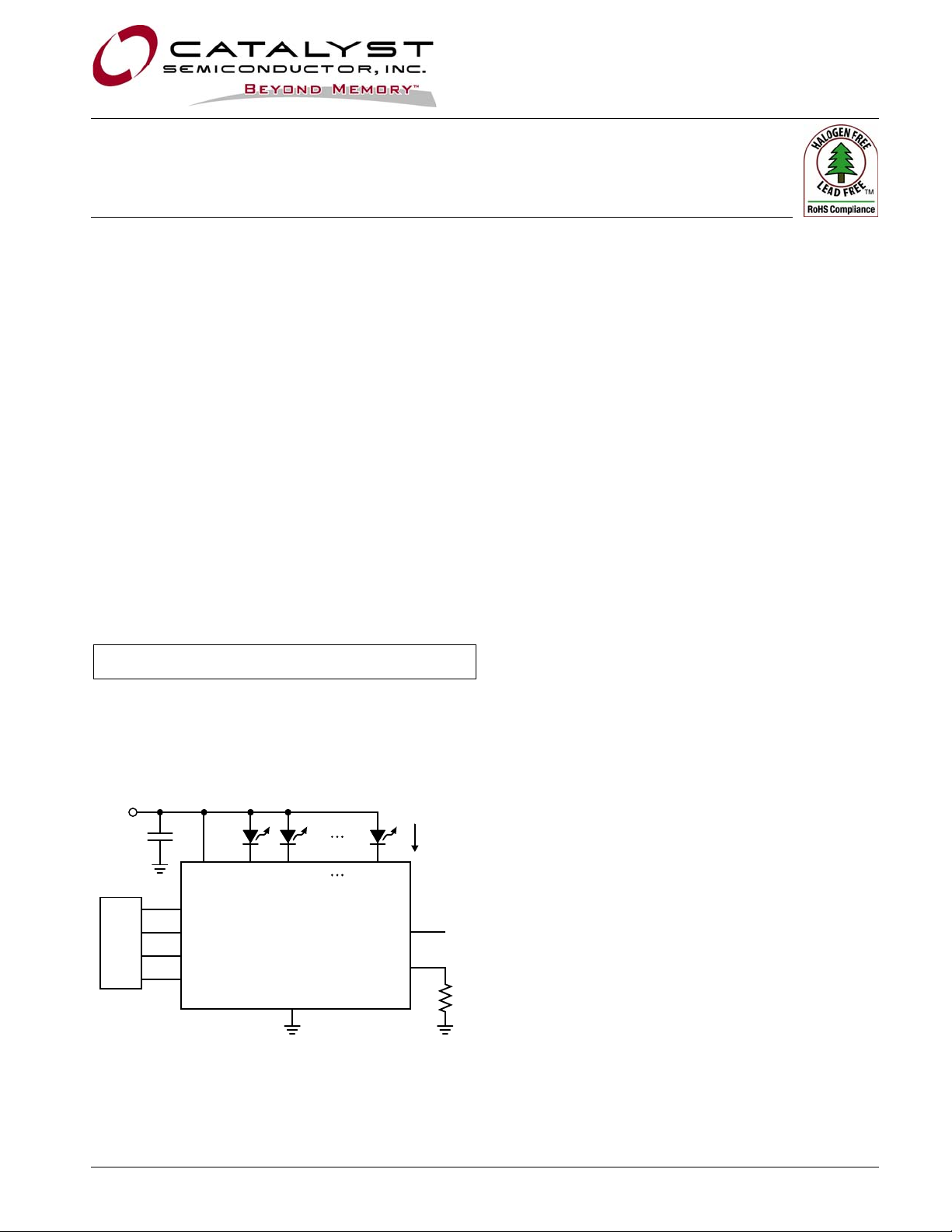
TYPICAL APPLICATION CIRCUIT
VIN
3V to
5.5V
CONTROLLER
© Catalyst Semiconductor, Inc. 1 Doc. No. MD-5028 Rev. C
Characteristics subject to change without notice
1µF
BLANK
LATCH
SIN
CLK
LED1VDD
LED2
CAT4016
GND
LED16
SOUT
RSET
20mA
to nex
device
3k
CAT4016
ORDERING INFORMATION
Part Number Package Quantity per Reel Package Marking
CAT4016W-T1 SOIC24
CAT4016Y-T2 TSSOP24
CAT4016VS-T2 QSOP24
CAT4016VSR-T2 QSOP24
CAT4016HV6-T2 TQFN24
CAT4016HV6-GT2 TQFN24
Notes:
(1) Matte-Tin Plated Finish (RoHS-compliant)
(2) NiPdAu Plated Finish (RoHS-compliant)
(1)
1,000 CAT4016W
(1)
2,000 CAT4016Y
(1)
2,000 4016VS
(1)
2,000 4016VSR
(1)
2,000 LAAA
(2)
2,000 LAAD
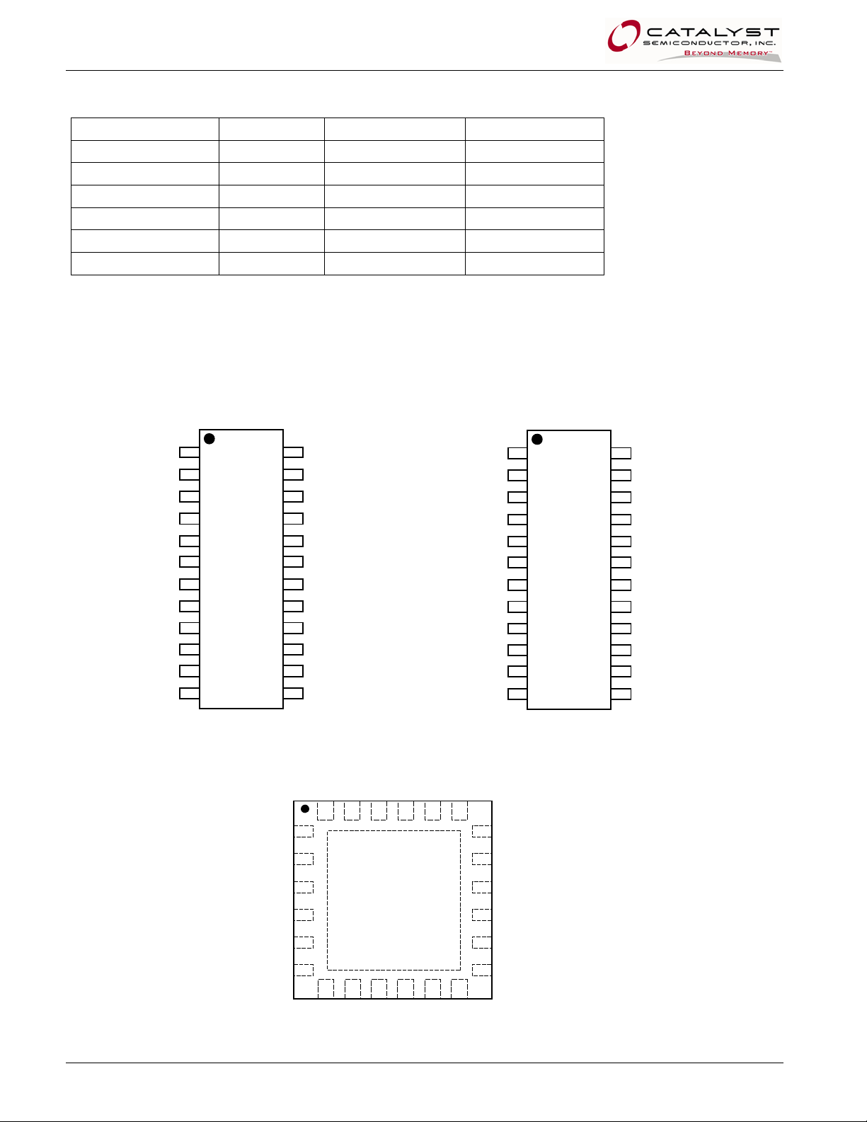
PIN CONFIGURATION
24-Lead SOIC (W),
TSSOP (Y), QSOP (VS)
24-Lead QSOP (VSR)
GND
SIN
CLK
LATCH
LED1
LED2
LED3
LED4
LED5
LED6
LED7
LED8
124
223
322
421
520
619
718
817
916
10 15
11 14
12 13
VDD
RSET
SOUT
BLANK
LED16
LED15
LED14
LED13
LED12
LED11
LED10
LED9
LED15
LED16
BLANK
SOUT
RSET
VDD
GND
SIN
CLK
LATCH
LED1
LED2
124
223
322
421
520
619
718
817
916
10 15
11 14
12 13
LED14
LED13
LED12
LED11
LED10
LED9
LED8
LED7
LED6
LED5
LED4
LED3
GND
24-Lead TQFN (HV6)
RSET
VDD
1
BLANK
LED16
SOUT
21222324
LED15
1920
LED14
18
2
SIN
CLK
LATCH
LED1
LED2
3
4
5
6
10987
LED3
LED4
LED5
LED7
LED6
1211
LED8
LED13
17
16
LED12
15
LED11
1413LED10
LED9
Doc. No. MD-5028 Rev. C 2 © Catalyst Semiconductor, Inc.
Characteristics subject to change without notice
CAT4016
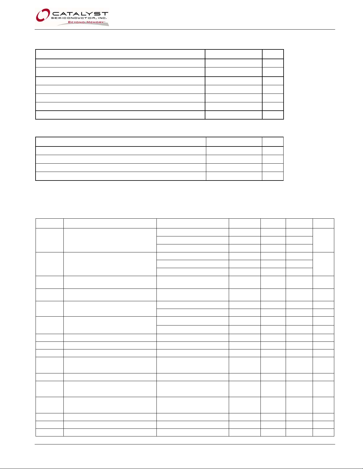
ABSOLUTE MAXIMUM RATINGS
Parameter Rating Units
VDD Supply Voltage 6 V
Logic input/output voltage (SIN, SOUT, CLK, BLANK, LATCH) -0.3V to VDD+0.3V V
LEDn voltage 6 V
DC output current on LED1 to LED16 150 mA
Storage Temperature Range -55 to +160
Junction Temperature Range -40 to +150
Lead Soldering Temperature (10sec.) 300
°C
°C
°C
RECOMMENDED OPERATING CONDITIONS
Parameter Range Units
VDD 3.0 to 5.5 V
Voltage applied to LED1 to LED16 0.4 to 5.5 V
LED current RSET control range up to 100 mA
Ambient Temperature Range -40 to +85
°C
ELECTRICAL OPERATING CHARACTERISTICS
DC Characteristics
V
= 5.0V, T
DD
= 25 ºC, over recommended operating conditions unless specified otherwise.
AMB
Symbol Name Conditions Min Typ Max Units
V
= 1V, R
LED
I
LED Current (any channel)
LED-ACC
I
LED-MAT
ΔI
VDD
ΔI
VLED
I
DDOFF
I
DDON
I
LKG
R
LATCH
R
BLANK
V
VIL
V
HYS
IIL
V
OH
VOL
V
RSET
LED Current Matching
- I
(I
LED
LEDAVR
) / I
LEDAVR
LED current regulation vs. V
LED current regulation vs. V
DD
LED
Supply Current (all outputs off)
Supply Current (all outputs on)
LEDn output Leakage V
LATCH Pull-down Resistance 100 180 300 k
BLANK Pull-up Resistance 100 180 300 k
Logic high input voltage
IH
Logic low input voltage
Logic input hysteresis voltage
Logic Input leakage current
(CLK, SIN)
SOUT logic high output voltage
SOUT logic low output voltage
RSET Regulated Voltage 1.17 1.20 1.23 V
V
= 1V, R
LED
= 1V, R
V
LED
V
= 1V, R
LED
V
= 1V, R
LED
V
= 1V, R
LED
within 4.5V and 5.5V
V
DD
LED current 30mA
within 1V and 3V
V
LED
LED current 30mA
R
= 3k 3 8 mA
SET
R
= 750 8.5 mA
SET
R
= 3k 4 9 mA
SET
R
= 750 10 mA
SET
= 5V, outputs off -1 1 µA
LED
VI = VDD or GND -5 0 5 µA
= -1mA
I
OH
I
= 1mA
OL
TSD Thermal Shutdown 160 ºC
T
Thermal Hysteresis 20 ºC
HYST
= 3k 18 20 22
SET
= 1.5k 36 40 44
SET
= 750 80
SET
= 3k ±1.5
SET
= 1.5k -6.0 ±1.5 +6.0
SET
= 750 ±2.0
SET
±0.1 % / V
±0.05 % / V
0.7xV
V
CC
DD
-0.3V
0.1xVDD V
0.3xVDD V V
0.3
mA
%
V
© Catalyst Semiconductor, Inc. 3 Doc. No. MD-5028 Rev. C
Characteristics subject to change without notice
CAT4016
V
Timing Characteristics
For 3.0V ≤ V
≤ 5.5V, T
DD
= 25 ºC, unless specified otherwise.
AMB
Symbol Name Conditions Min
(1)
Typ
(2)
Max
CLK
f
CLK Clock Frequency 25 MHz
clk
t
CLK Pulse Width High 20 ns
cwh
t
CLK Pulse Width Low 20 ns
cwl
SIN
t
Setup time SIN to CLK 4 ns
ssu
tsh Hold time SIN to CLK 4 ns
LATCH
t
LATCH Pulse width 20 ns
lwh
Tlh Hold time LATCH to CLK 4 ns
T
Setup time LATCH to CLK Channel Stagger Delay 800 ns
lsu
LEDn
tld LED1 Propagation delay LATCH to LED1 off/on 40 300 ns
tls LED Propagation delay stagger LED(n) to LED(n+1) 17 40 ns
t
lst
LED Propagation delay stagger
total
LED1 to LED16 250 ns
tbd BLANK Propagation delay BLANK to LED(n) off/on 60 300 ns
tlr LED rise time (10% to 90%) Pull-up resistor = 5 0 to 3 . 0V 40 200 ns
tlf LED fall time (90% to 10%) Pull- up resistor = 50 t o 3 . 0 V 30 250 ns
SOUT
tor SOUT rise time (10% to 90%) CL = 15pF 5 ns
tof SOUT fall time (90% to 10%) CL = 15pF 5 ns
tod Propagation delay time SOUT CLK to SOUT 8 15 25 ns
(1)
Units
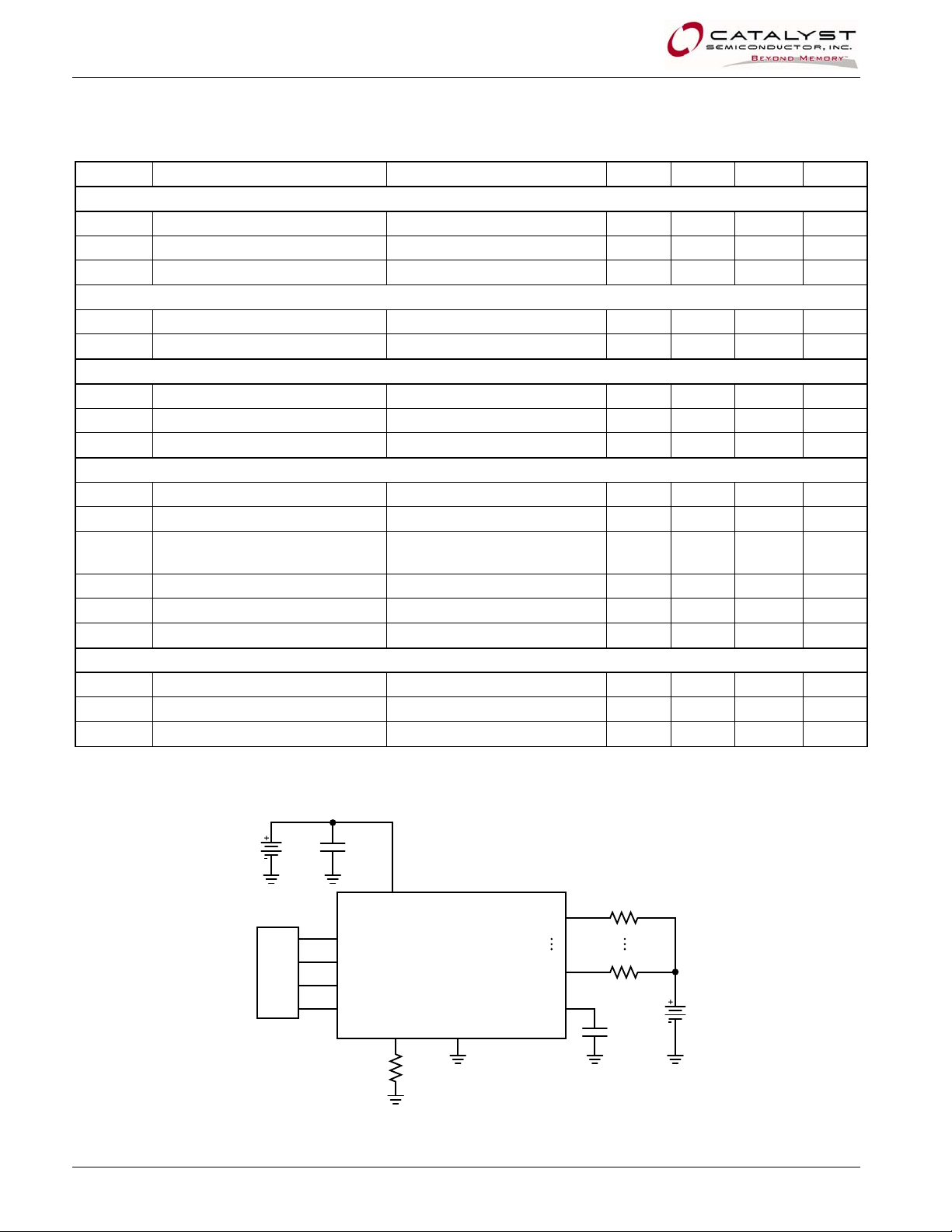
Test Circuit for AC Characteristics
DD
CONTROLLER
Notes:
(1) All min and max values are guaranteed by design.
(2) V
Doc. No. MD-5028 Rev. C 4 © Catalyst Semiconductor, Inc.
= 5V, LED current 30mA.
DD
1µF
BLANK
LATCH
SIN
CLK
RSET
VDD
RSET
CAT4016
GND
LED1
LED16
SOUT
Rp 50
Rp 50
Cl
15pF
V1
3V
Characteristics subject to change without notice
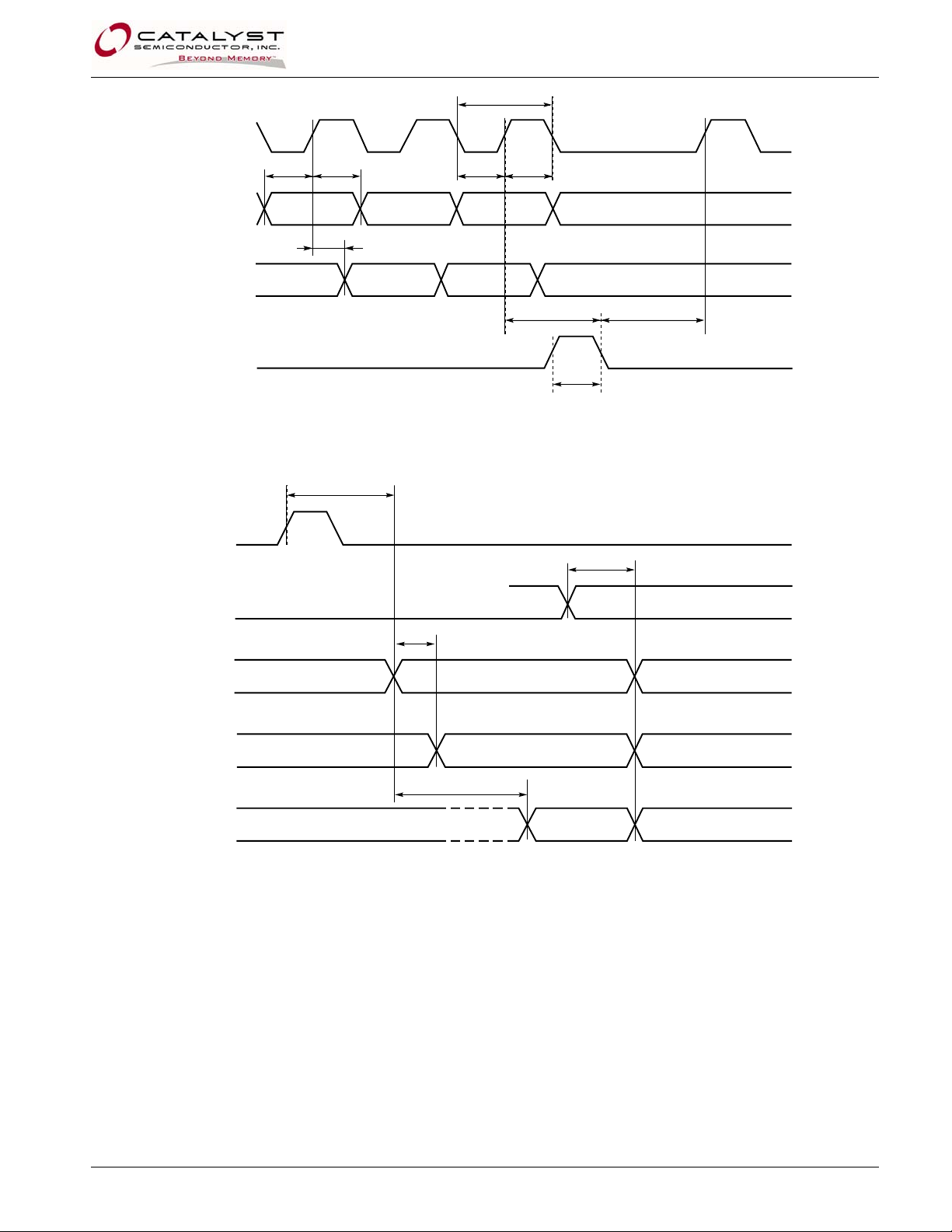
CAT4016
1/f
clk
CLK
t
ssu
t
sh
t
cwl
t
cwh
SIN
t
od
SOUT
t
lh
t
lsu
LATCH
t
lwh
Figure 1. Serial Input Timing Diagram
LATCH
BLANK
t
ld
t
bd
LED1
LED2
LED16
t
ls
t
= 15 t
lst
ls
Figure 2. LED Output Timing Diagram
© Catalyst Semiconductor, Inc. 5 Doc. No. MD-5028 Rev. C
Characteristics subject to change without notice

CAT4016
TYPICAL PERFORMANCE CHARACTERISTICS
V
= 5.0V, LED current 30mA, all LEDs On, T
DD
LED Current vs. LED Pin Voltage
70
60
50
40
30
20
LED CURRENT [mA]
10
0
0.0 0.3 0.6 0.9 1.2 1.5
LED PIN [V]
LED Current vs. VDD Pin Voltage
31.5
31.0
= 25°C unless otherwise specified.
AMB
Supply Current vs. VDD Pin Voltage
6.0
All LED's ON
5.5
5.0
4.5
4.0
3.5
SUPPLY CU RRENT [mA]
All LED's OFF
3.0
3.0 3.5 4.0 4.5 5.0 5.5
VDD [V]
Supply Current vs. RSET Current
12
All LED's ON
10
30.5
30.0
29.5
LED CURRENT [mA]
29.0
28.5
3.0 3.5 4.0 4.5 5.0 5.5
VDD [V ]
RSET Voltage vs. VDD Pin Voltage
1.30
1.25
1.20
RSET PIN [V]
1.15
1.10
3.0 3.5 4.0 4.5 5.0 5.5
VDD [V]
8
6
4
All LED's OFF
2
SUPPLY CURRENT [mA]
0
0.0 0.5 1.0 1.5 2.0
RSET CURRENT [mA]
LED Current vs. RSET Resistor
100
80
60
40
20
LED CURRENT [mA]
0
0.1 1.0 10.0 100.0
RSET [kΩ]
Doc. No. MD-5028 Rev. C 6 © Catalyst Semiconductor, Inc.
Characteristics subject to change without notice

CAT4016
TYPICAL PERFORMANCE CHARACTERISTICS
V
= 5.0V, LED current 30mA, all LEDs On, T
DD
RSET Voltage vs. Temperature
1.30
1.25
= 25°C unless otherwise specified.
AMB
LED Current vs. Temperature
31.5
31.0
30.5
1.20
RSET PIN [V]
1.15
1.10
-50 0 50 100 150
TEMPERATURE [°C]
Internal Pull-Down Current (LATCH pin)
30
25
20
15
10
5
PULL -DO WN CURRENT [A] .
0
012345
LATCH VOLTAGE [ V]
PWM Dimming on BLANK pin (f = 10kHz)
30.0
29.5
LED CURRENT [mA]
29.0
28.5
-50 0 50 100 150
TEMP ERA TURE [°C]
Internal Pull-Up Current (BLANK pin)
30
25
20
15
10
5
PULL-UP CURRENT [A] .
0
012345
BLANK VOLTAGE [V]
BLANK Transient Response
100
80
60
40
DUTY CYCLE [%]
20
0
0 5 10 15 20 25 30
LED CURRE NT [ m A]
© Catalyst Semiconductor, Inc. 7 Doc. No. MD-5028 Rev. C
Characteristics subject to change without notice

CAT4016
PIN DESCRIPTION
Name Function
GND Ground
SIN Serial data input pin
CLK Serial clock input pin
LATCH Latch serial data to output registers
LED1-LED16 LED channel 1 to 16 cathode terminals
BLANK Enable / disable all channels
SOUT Serial data output pin.
RSET LED current set pin
VDD Positive supply Voltage
TAB (TQFN
package only)
Connect to GND on the PCB
PIN FUNCTION
GND is the ground reference pin for the device. This
pin must be connected to the ground plane on the
PCB.
SIN is the serial data input. Data is loaded into the
internal register on each rising edge of CLK.
CLK is the serial clock input. On each rising CLK
edge, data is transferred from SIN to the internal 16bit serial shift register.
LATCH is the latch data input. On the rising edge of
LATCH, data is loaded from the 16-bit serial shift
register into the output register latch. On the falling
edge, this data is latched in the output register and
isolated from the state of the serial shift register.
LED1 - LED16 are the LED current sink channels.
These pins are connected to the LED cathodes. The
current sinks drive the LEDs with a current equal to 50
times RSET pin current. For the LED sink to operate
correctly, the voltage on the LED pin must be above
0.4V.
BLANK is the LED channel enable and disable input
pin. When low, LEDs are enabled according to the
output latch register content. When high, all LEDs are
off, while preserving the data in the output latch
register.
SOUT is the serial data output of the 16-bit serial shift
register. This pin is used to cascade several devices
on the serial bus. The SOUT pin is then connected to
the SIN input of the next device on the serial bus to
cascade.
RSET is the LED current setting pin. A resistor is
connected between this pin and ground. Each LED
channel current is set to 50 times the current pulled
out of the pin. The RSET pin voltage is regulated to
1.2V.
VDD is the positive supply pin voltage for the entire
device. A small 1µF ceramic is recommended close
to pin.
Doc. No. MD-5028 Rev. C 8 © Catalyst Semiconductor, Inc.
Characteristics subject to change without notice

CAT4016
BLOCK DIAGRAM
LED1 LED2 LED3 LED16
VDD
VIN
BLANK
LATCH
SIN
CLK
+
L1 L2 L3
S1 S2 S3
CURRENT
LATCHES
REGISTER
Figure 2. CAT4016 Functional Block Diagram
BASIC OPERATION
The CAT4016 uses 16 tightly matched current sinks to
accurately regulate the LED current in each channel.
The external resistor, R
channel current to 50 times the current in R
Tight current regulation for all channels is possible
over a wide range of input and LED voltages due to
independent current sensing circuitry on each
channel. The LED channels have a maximum dropout
of 0.4V for most current and supply voltage
conditions. This helps improve the heat dissipation
and efficiency of the LED driver.
Upon power-up, an under-voltage lockout circuit
clears all latches and shift registers and sets all
outputs to off. Once the under-voltage lockout
threshold has been reached the device can be
programmed.
The driver delays the activation of each consecutive
LED output channel by 17ns (typical). Relative to
LED1, LED2 is delayed by 17ns, LED3 by 34ns and
LED16 by 250ns typical. The delay is introduced when
LATCH is activated. The delay minimizes the inrush
current on the LED supply by staggering the turn on
and off current spikes over a period of time and
therefore allowing usage of smaller bypass capacitors.
, is used to set the LED
SET
.
SET
50 current LED ×=
2.1
R
SET
+
SINKS
SHIFT
Current
Setting
1.2V Ref
L16
S16
RSET
GND
SOUT
Pull-up and pull-down resistors are internally provided
to set the state of the BLANK and LATCH pins to the
off-state when not externally driven.
SERIAL INTERFACE
A high-speed serial 4-wire interface is provided to
program the state of each LED on or off. The
interface contains a 16-bit serial to parallel shift
register (S1-S16) and a 16-bit latch (L1-L16).
Programming the serial to parallel register is
accomplished via SIN and CLK input pins. On each
rising edge of the CLK signal, the data from SIN is
moved through the shift register serially. Data is also
moved out of SOUT which can be connected to a next
device if programming more then one device on the
same interface.
On the rising edge of LATCH, the data contents of the
serial to parallel shift register is reflected in the
latches. On the falling edge of LATCH, the state of the
serial to parallel register at that particular time is
saved in the latches and does not change irrespective
of the contents of the serial to parallel register.
BLANK is used to disable all LEDs (turn off)
simultaneously while maintaining the same data in the
latch register. When low, the LED outputs reflect the
data in the latches. When high, all outputs are high
impedance (zero current).
© Catalyst Semiconductor, Inc. 9 Doc. No. MD-5028 Rev. C
Characteristics subject to change without notice

CAT4016
PACKAGE OUTLINE DRAWINGS
SOIC 24-Lead 300mils (W)
b
PIN#1 IDENTIFICATION
(1)
e
E1 E
SYMBOL MIN NOM MAX
A2.35 2.65
A1 0.10 0.30
A2 2.05 2.55
b0.31 0.51
c0.20 0.33
D 15.20 15.40
E 10.11 10.51
E1 7.34 7.60
e1.27 BSC
h0.25 0.75
L0.40 1.27
0° 8°
15° 15°
TOP VIEW
D
A
SIDE VIEW END VIEW
A2
A1
h
h
L
1
1
c
For current Tape and Re el infor mation, do wnload the P DF fil e fro m:
http://www.catsemi.com/documents/tapeandreel.pdf.
Notes:
(1) All dimensions are in millimeters. Angles in degrees.
(2) Complies with JEDEC MS-013.
Doc. No. MD-5028 Rev. C 10 © Catalyst Semiconductor, Inc.
Characteristics subject to change without notice

CAT4016
A
(1)
TSSOP 24-Lead 4.4mm (Y)
b
SYMBOL MIN NOM MAX
A1.20
A1 0.05 0.15
A2 0.80 1.05
b 0.19 0.30
E1 E
c 0.09 0.20
D 7.70 7.80 7.90
E 6.25 6.40 6.55
E1 4.30 4.40 4.50
e 0.65 BSC
L 1.00 REF
L1 0.50 0.60 0.70
10° 8°
A2
e
TOP VIEW
D
A
1
1
SIDE VIEW END VIEW
c
L1
L
For current Tape and Re el infor mation, do wnload the P DF fil e fro m:
http://www.catsemi.com/documents/tapeandreel.pdf.
Notes:
(1) All dimensions are in millimeters. Angles in degrees.
(2) Complies with JEDEC MO-153.
© Catalyst Semiconductor, Inc. 11 Doc. No. MD-5028 Rev. C
Characteristics subject to change without notice

CAT4016
(1)
QSOP 24-Lead (VS, VSR)
e
D
b
SYMBOL MIN NOM MAX
A1.37 1.73
A1 0.10 0.25
b0.20 0.31
c0.19 0.25
D8.56 8.74
E
1
E
E5.82 6.19
E1 3.81 3.98
e 0.635 BSC
h0.28 0.48
L0.41 0.86
L2 0.254 BSC
10º 8º
27º BSC
TOP VIEW
h
2
L
END VIEW
SIDE VIEW
2
A
1
A
c
For current Tape and Re el infor mation, do wnload the P DF fil e fro m:
http://www.catsemi.com/documents/tapeandreel.pdf.
1
L
Notes:
(1) All dimensions are in millimeters. Angles in degrees.
(2) Complies with JEDEC MO-137.
Doc. No. MD-5028 Rev. C 12 © Catalyst Semiconductor, Inc.
Characteristics subject to change without notice

CAT4016
TQFN 24-Pad 4 x 4mm (HV6)
D
PIN#1 INDEX AREA
(1
A
DETAIL A
E
A1
SIDE VIEWTOP VIEW BOTTOM VIEW
E2
PIN#1 ID
D2
b
e
SYMBOL MIN NOM MAX
L
A 0.70 0.75 0.80
A1 0.00 0.02 0.05
A3 0.20 REF
DETAIL A
b 0.18 0.25 0.30
D 3.90 4.00 4.10
D2 2.40 – 2.90
E 3.90 4.00 4.10
E2 2.40 – 2.90
A
e0.50 BSC
L 0.30 0.40 0.50
FRONT VIEW
A3
)
For current Tape and Re el infor mation, do wnload the P DF fil e fro m:
http://www.catsemi.com/documents/tapeandreel.pdf.
Notes:
(1) All dimensions are in millimeters. Angles in degrees.
(2) Complies with JEDEC MO-220.
© Catalyst Semiconductor, Inc. 13 Doc. No. MD-5028 Rev. C
Characteristics subject to change without notice

CAT4016
,
EXAMPLE OF ORDERING INFORMATION
Prefix
CAT 4016 HV6 – G T2
Optional
Company ID
Device # Suffix
Product Number
4016
Package
W: SOIC
Y: TSSOP
VS: QSOP
VSR: QSOP
HV6: TQFN
(1)
Tape & Reel
T: Tape & Reel
1: 1,000/Reel
000/Reel
2: 2
Lead Finish
Blank: Matte-Tin
(4)
G: NiPdAu
(5)
For Product Top Mark Codes, click here:
http://www.catsemi.com/techsupport/producttopmark.asp
Notes:
(1) All packages are RoHS-compliant (Lead-free, Halogen-free).
(2) The device used in the above example is a CAT4016HV6–GT2 (TQFN, NiPdAu, Tape & Reel, 2,000/Reel).
(3) For additional package and temperature options, please contact your nearest Catalyst Semiconductor Sales office.
(4) Different pin outs, see page 2.
(5) SOIC package availability in 1,000/Reel. All other packages are 2,000/Reel.
Doc. No. MD-5028 Rev. C 14 © Catalyst Semiconductor, Inc.
Characteristics subject to change without notice

REVISION HISTORY
Date Rev. Reason
09/26/2007 A Initial Issue
10/17/2007 B Update Absolute Maximum Ratings
Update Ordering Information table, added TQFN in NiPdAu plated finish.
04/09/2008 C
Copyrights, Trademarks and Patents
© Catalyst Semiconductor, Inc.
Trademarks and registered trademarks of Catalyst Semiconductor include each of the following:
Adaptive Analog™, Beyond Memory™, DPP™, EZDim™, LDD™, MiniPot™, Quad-Mode™ and Quantum Charge Programmable™
Catalyst Semiconductor has been issued U.S. and foreign patents and has patent applications pending that protect its product s.
CATALYST SEMICONDUCTOR MAKES NO WARRANTY, REPRESENTATION OR GUARANTEE, EXPRESS OR IMPLIED, REGARDING THE SUITABILITY OF ITS
PRODUCTS FOR ANY PARTICULAR PURPOSE, NOR THAT THE USE OF ITS PRODUCTS WILL NOT INFRINGE ITS INTELLECTUAL PROPERTY RIGHTS OR
THE RIGHTS OF THIRD PARTIES WITH RESPECT TO ANY PARTICULAR USE OR APPLICATION AND SPECIFICALLY DISCLAIMS ANY AND ALL LIABILITY
ARISING OUT OF ANY SUCH USE OR APPLICATION, INCLUDING BUT NOT LIMITED TO, CONSEQUENTIAL OR INCIDENTAL DAMAGES.
Catalyst Semiconductor products are not designed, intended, or authorized for use as components in systems intended for surgical implant into the body, or other
applications intended to support or sustain life, or for any other application in which the failure of the Catalyst Semiconductor product could create a situation where
personal injury or death may occur.
Catalyst Semiconductor reserves the right to make changes to or discontinue any product or service described herein without notice. Products with data sheets labeled
"Advance Information" or "Preliminary" and other products described herein may not be in production or offered for sale.
Catalyst Semiconductor advises customers to obtain the current version of the relevant product information before placing orders. Circuit diagrams illustrate typical
semiconductor applications and may not be complete.
Update Package Outline Drawings
Update Example of Ordering Information
Add Top Mark Codes link
Catalyst Semiconductor, Inc.
Corporate Headquarters
2975 Stender Way
Santa Clara, CA 95054
Phone: 408.542.1000 Document No: MD-5028
Fax: 408.542.1200 Revision: C
www.catsemi.com Issue date: 04/09/08
 Loading...