3-Channel Ultra High Efficiency Quad-Mode™ LED Driver
CAT3643
FEATURES
High efficiency 1.33x charge pump
Quad-mode charge pump: 1x, 1.33x, 1.5x, 2x
Drives up to 3 LEDs at 32mA each
1-wire EZDim™ LED current programming
Power efficiency up to 92%
Low noise input ripple in all modes
“Zero” current shutdown mode
Soft start and current limiting
Short circuit protection
Thermal shutdown protection
Tiny 12-pad XQFN, 12-pad TDFN and 16-pad
TQFN packages
APPLICATION
LCD Display Backlight
Cellular Phones
Digital Still Cameras
Handheld Devices
DESCRIPTION
The CAT3643 is a high efficiency Quad-ModeTM
fractional charge pump that can drive up to three
LEDs programmable by a one wire digital interface.
The inclusion of a 1.33x fractional charge pump mode
increases device efficiency by up to 10% over
traditional 1.5x charge pumps with no added external
capacitors.
Low noise input ripple is achieved by operating at a
constant switching frequency which allows the use of
small external ceramic capacitors. The multi-fractional
charge pump supports a wide range of input voltages
from 2.4V to 5.5V.
The EN/DIM logic input functions as a chip enable and
a digital dimming interface for current setting of all
LEDs. Six different current ratios are available via the
interface.
The device is available in the tiny 12-pad XQFN 2.5 x
2.5mm with max height of 0.4mm or in 16-pad TQFN
or 12-pad TDFN 3mm x 3mm package with a max
height of 0.8mm.
ORDERING INFORMATION
Part Number Package Marking
CAT3643HV2-T2 TDFN-12 3 x 3
CAT3643HV2-GT2 TDFN-12 3 x 3
CAT3643HV3-T2 TQFN-16 3 x 3
CAT3643HV3-GT2 TQFN-16 3 x 3
CAT3643HL1-T2 XQFN-12 2.5 x 2.5
Notes:
(1) Matte-Tin Plated Finish (RoHS-compliant)
(2) NiPdAu Plated Finish (RoHS-compliant)
(3) Quantity per reel is 2000
(1)
HABF
(2)
HABG
(1)
JAAE
(2)
JAAF
(1)
For Ordering Information details, see page 16.
LB
TM
Catalyst Semiconductor’s Quad-Mode
1.33x charge
pump switching architecture is patented.
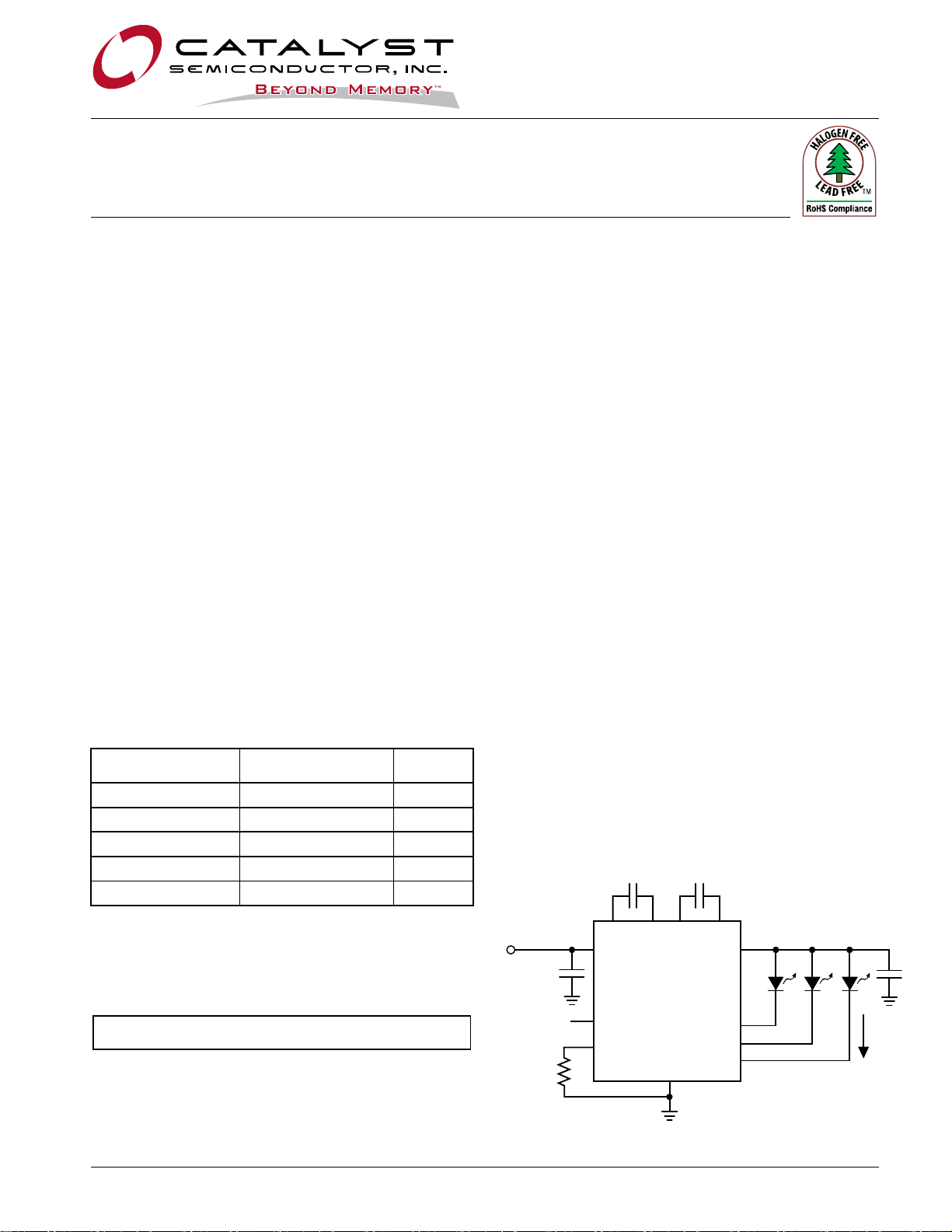
TYPICAL APPLICATION CIRCUIT
V
IN
C
2.4V
to
1µF
5.5V
1-Wire
EZDim
Programming
4.02k
IN
TM
V
IN
EN/DIM
RSET
1µF
C1-C1+ C2-C2+
CAT3643
GND
1µF
V
OUT
LED1
LED2
LED3
V
OUT
20mA
C
1µF
OUT
© Catalyst Semiconductor, Inc. 1 Doc. No. MD-5022 Rev. E
Characteristics subject to change without notice
CAT3643
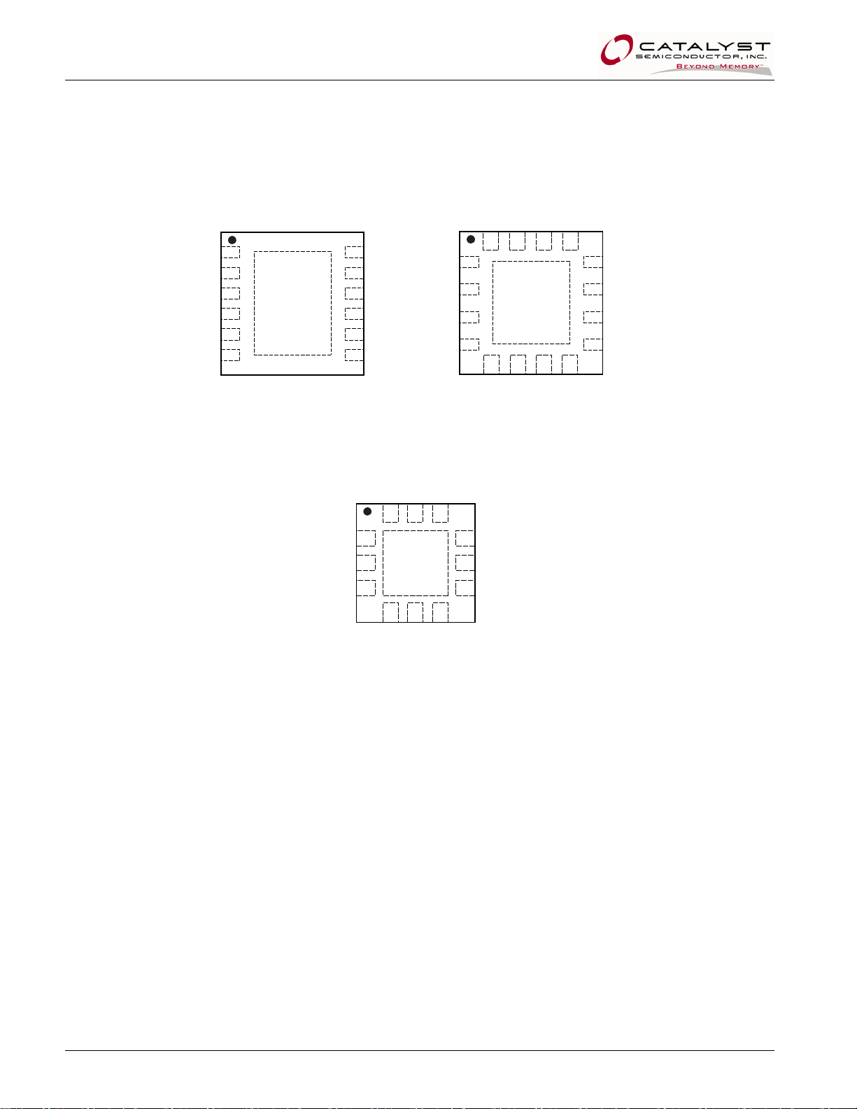
PIN CONFIGURATION
TDFN 12-Pad 3 x 3mm
(Top View)
1
LED1
211LED2 C2+
3
LED3
4
RSET
58EN/DIM C1+
6
VOUT
12
10
GND
C2-
9
C1-
7
VIN
TQFN 16-Pad 3 x 3mm
(Top View)
LED1
GND
NC
1
LED2
2
LED3
3
NC
4
RSET
EN/DIM
VOUT
NC
13141516
NC
8765
VIN
12
11
10
C2-
C2+
C1-
9
C1+
XQFN 12-Pad 2.5 x 2.5mm
(Top View)
C2-
GND
C2+
1
2
C1+
C1-
101112
9
VIN
VOUT
8
3
LED1
LED2
The CAT3643 is offered in three different packages.
The 12-pad TDFN 3mm x 3mm with a max height of
0.8mm is pin-compatible to the Catalyst CAT3603
LED driver. The 12-pad XQFN provides the smallest
7
EN/DIM
654
LED3
RSET
footprint with a package size of 2.5mm x 2.5mm and
0.4mm max height. The 16-pad TQFN 3mm x 3mm
with max height of 0.8mm is also offered.
Doc. No. MD-5022 Rev. E 2 © Catalyst Semiconductor, Inc.
Characteristics subject to change without notice

CAT3643
ABSOLUTE MAXIMUM RATINGS
Parameter Rating Unit
VIN, LEDx, C1±, C2±, EN/DIM, RSET voltage 6 V
V
voltage 7 V
OUT
Storage Temperature Range -65 to +160
Junction Temperature Range -40 to +150
RECOMMENDED OPERATING CONDITIONS
Parameter Rating Unit
VIN 2.5 to 5.5 V
Ambient Temperature Range -40 to +85
I
per LED pin up to 30 mA
LED
LED Forward Voltage Range 1.3 to 4.3 V
Typical application circuit with external components is shown on page 1.
ELECTRICAL OPERATING CHARACTERISTICS
(over recommended operating conditions unless specified otherwise) V
Symbol Name Conditions Min Typ Max Units
1x mode, no load
IQ Quiescent Current
1.33 x mode, no load
1.5x mode, no load
2x mode, no load
I
Shutdown Current VEN = 0V 1 µA
QSHDN
(I
– I
I
I
LED Current Accuracy
LED-ACC
LED Channel Matching (I
LED-DEV
V
RSET Regulated Voltage
RSET
LEDAVG
RSET = 5k
LED
- I
NOMINAL
LEDAVG
) / I
1x mode
R
Output Resistance (open loop)
OUT
1.33x mode, V
1.5x mode, V
2x mode, V
F
OSC
I
SC_MAX
I
IN_MAX
LEDTH
V
HYS
T
DF
R
EN/DIM
VHI
V
LO
Charge Pump Frequency
Output short circuit Current Limit V
Input Current Limit V
1x to 1.33x or 1.33x to 1.5x or 1.5x to 2x
Transition Thresholds at any LED pin
1x Mode Transition Hysteresis 400 mV
Transition Filter Delay 500 µs
EN/DIM Pin
• Internal Pull-down Resistor
• Logic High Level
• Logic Low Level
1.33x and 2x mode
1.5x mode
< 0.5V 50 mA
OUT
> 1V 250 mA
OUT
130 mV
IN
= 2.7V
IN
= 2.4V
IN
TSD Thermal Shutdown 150
T
Thermal Hysteresis 20
HYS
V
Undervoltage lockout (UVLO) threshold 1.6 1.8 2.0 V
UVLO
°C
°C
°C
= 3.6V, EN = High, T
IN
= 25°C
AMB
1.0
1.7
2.2
2.4
) / I
NOMINAL
±1.5 %
LEDAVG
±2 %
0.58 0.6 0.62 V
0.8
= 3V
5
5
10
0.8
1
1.3
1
1.3
100
1.3
1.6
0.4
mA
mA
mA
mA
MHz
MHz
k
V
V
°C
°C
© Catalyst Semiconductor, Inc. 3 Doc. No. MD-5022 Rev. E
Characteristics subject to change without notice
CAT3643
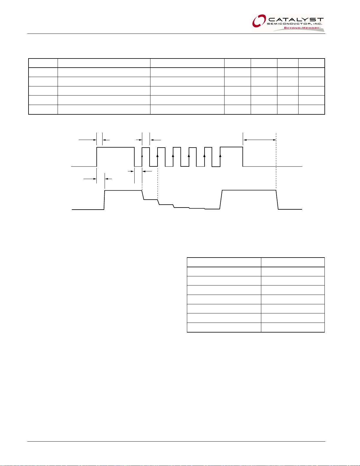
RECOMMENDED EN/DIM TIMING
For 2.4V ≤ V
Symbol Name Conditions Min Typ Max Units
T
SETUP
TLO EN/DIM program low time 0.2 100 s
THI EN/DIM program high time 0.2 s
T
PWRDWN
T
LED current settling time 40 s
LED
≤ 5.5V, over full ambient temperature range -40ºC to +85ºC.
IN
EN/DIM setup from shutdown 10 s
EN/DIM low time to shutdown 1.5 ms
T
PWRDWN
EN/DIM
T
SETUP
T
LED
T
HI
T
LO
100%
50%
LED
Current
Shutdown
25%
Figure 1. EN/DIM Digital Dimming Timing Diagram
LED Current Setting
The nominal LED current is set by the external
resistor connected between the RSET pin and
ground. Table 1 lists standard resistor values for
several LED current settings.
12.5%
100%
6.25%
3.12%
Shutdown
LED Current (mA) RSET (kΩ)
2 40.0
5 15.8
10 7.87
15 5.23
20 4.02
25 3.16
30 2.67
Table 1. Resistor RSET and LED Current
Doc. No. MD-5022 Rev. E 4 © Catalyst Semiconductor, Inc.
Characteristics subject to change without notice
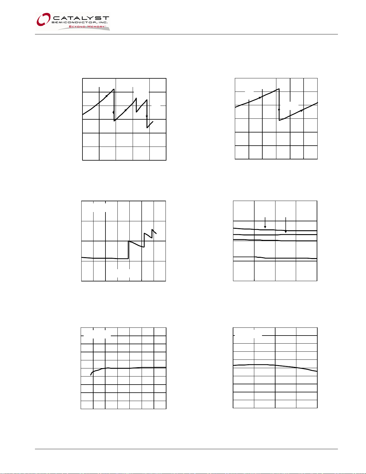
TYPICAL PERFORMANCE CHARACTERISTICS
.
.
V
= 3.6V, I
IN
= 60mA (3 LEDs at 20mA), CIN = C
OUT
Efficiency vs. Input Voltage
= C1 = C2 = 1F, T
OUT
= 25°C unless otherwise specified.
AMB
Efficiency vs. Li-Ion Voltage
CAT3643
100
VF = 3.3V
90
1.33x
1.5x
1x
80
2x
70
60
EFFICIENCY [%]
50
40
INPUT VOLTAGE [V]
Quiescent Current vs. Input Voltage
4.0
VF = 3.3V
3.0
2.0
100
VF = 3.3V
90
80
70
60
EFFICIENCY [%]
50
40
2.02.53.03.54.04.5
1x
1.33x
3.03.23.43.63.84.04.2
INPUT VOLTAGE [V]
Quiescent Current vs. Temperature
4.0
2x 1.5x
3.0
2.0
1.33x
1.0
QUIESCENT CURRENT [ mA]
0.0
LEDs Off
2.02.53.03.54.04.55.05.5
INPUT VOLTAGE [V]
1.0
QUIESCENT CURRENT [mA]
0.0
-40 0 40 80 120
TEMPERATURE [°C]
1x
LED Current Change vs. Input Voltage
10
VF = 3.3V
8
6
4
2
0
-2
-4
-6
-8
-10
LED CURRENT VARI ATION [ %]
2.0 2.5 3.0 3.5 4.0 4.5 5.0 5.5
INPUT VOLTAGE [V]
LED Current Change vs. Temperature
10
VF = 3.3V
8
6
4
2
0
-2
-4
-6
-8
-10
LED CURRENT VARIATION [%]
-40 0 40 80 120
TEMPERA TURE [°C]
© Catalyst Semiconductor, Inc. 5 Doc. No. MD-5022 Rev. E
Characteristics subject to change without notice
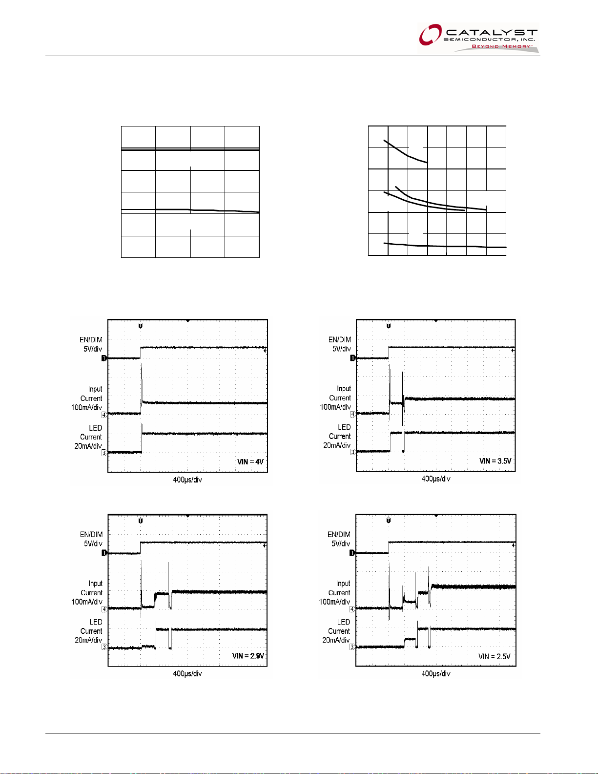
CAT3643
.
TYPICAL PERFORMANCE CHARACTERISTICS
V
= 3.6V, I
IN
= 60mA (3 LEDs at 20mA), CIN = C
OUT
Switching Frequency vs. Temperature
= C1 = C2 = 1F, T
OUT
= 25°C unless otherwise specified.
AMB
Output Resistance vs. Input Voltage
1.3
1.2
1.5x Mode
1.1
1.0
0.9
1.33x, 2x Mode
0.8
0.7
SWITCHING FREQUENCY [MHz]
-40 0 40 80 120
TEMPERATURE [°C]
Power Up in 1x Mode
12
10
8
6
1.5x
4
2
OUTPUT RESISTANCE []
0
2.0 2.5 3.0 3.5 4.0 4.5 5.0 5.5
2x
1.33x
1x
INPUT VOLTAGE [V]
Power Up in 1.33x Mode
Power Up in 1.5x Mode
Power Up in 2x Mode
Doc. No. MD-5022 Rev. E 6 © Catalyst Semiconductor, Inc.
Characteristics subject to change without notice

TYPICAL PERFORMANCE CHARACTERISTICS
V
= 3.6V, I
IN
= 60mA (3 LEDs at 20mA), CIN = C
OUT
Power Up Delay (1x Mode)
= C1 = C2 = 1F, T
OUT
= 25°C unless otherwise specified.
AMB
Power Down Delay (1x Mode)
CAT3643
Operating Waveforms in 1x Mode
Switching Waveforms in 1.5x Mode
Switching Waveforms in 1.33x Mode
Switching Waveforms in 2x Mode
© Catalyst Semiconductor, Inc. 7 Doc. No. MD-5022 Rev. E
Characteristics subject to change without notice

CAT3643
TYPICAL PERFORMANCE CHARACTERISTICS
V
= 3.6V, I
IN
= 60mA (3 LEDs at 20mA), CIN = C
OUT
Foldback Current Limit
= C1 = C2 = 1F, T
OUT
= 25°C unless otherwise specified.
AMB
LED Current vs. LED Pin Voltage
4.0
3.5
3.0
2.5
2.0
1.5
1.0
OUTPUT VOLTAGE [V]
0.5
0.0
0 100 200 300 400
OUTPUT CURRENT [mA]
Dimming Waveform
1x Mode
40
30
20
10
LED CURRE NT [mA]
0
0 50 100 150 200 250 300
LED PIN VOLTAGE [mV]
Line Transient Response
Disconnecting a Single LED
50
LED Current vs. RSET
40
30
20
10
LED CURRENT [mA ]
0
110100
RSET RESISTANCE [k]
Doc. No. MD-5022 Rev. E 8 © Catalyst Semiconductor, Inc.
Characteristics subject to change without notice

PIN DESCRIPTION
Name Function
LED1 LED1 cathode terminal.
LED2 LED2 cathode terminal.
LED3 LED3 cathode terminal.
RSET Connect resistor RSET to set the LED current.
EN/DIM Device enable (active high) and Dimming Control.
VOUT Charge pump output connected to the LED anodes.
VIN Charge pump input, connect to battery or supply.
C1+ Bucket capacitor 1 Positive terminal
C1- Bucket capacitor 1 Negative terminal
C2+ Bucket capacitor 2 Positive terminal
C2- Bucket capacitor 2 Negative terminal
GND Ground Reference
NC Not connected inside package.
GND Connect to GND on the PCB.
CAT3643
PIN FUNCTION
VIN is the supply pin for the charge pump. A small
1F ceramic bypass capacitor is required between the
VIN pin and ground near the device. The operating
input voltage range is from 2.5V to 5.5V. Whenever
the input supply falls below the under-voltage
threshold (1.8V), all the LED channels are disabled
and the device enters shutdown mode.
EN/DIM is the enable and one wire dimming input for
all LED channels. Levels of logic high and logic low
are set at 1.3V and 0.4V respectively. When EN/DIM
is initially taken high, the device becomes enabled
and all LED currents are set to the full scale according
to the resistor R
current” shutdown mode, the EN/DIM pin must be
held low for at least 1.5ms.
VOUT is the charge pump output that is connected to
the LED anodes. A small 1F ceramic bypass
capacitor is required between the VOUT pin and
ground near the device.
GND is the ground reference for the charge pump. The
pin must be connected to the ground plane on the PCB.
. To place the device into “zero
SET
C1+, C1- are connected to each side of the ceramic
bucket capacitor C
.
1
C2+, C2- are connected to each side of the ceramic
bucket capacitor C
.
2
LED1, LED2, LED3 provide the internal regulated
current sources for each of the LED cathodes. These
pins enter high-impedance zero current state whenever the device is placed in shutdown mode.
TAB is the exposed pad underneath the package. For
best thermal performance, the tab should be soldered
to the PCB and connected to the ground plane.
RSET is connected to the resistor (R
) to set the full
SET
scale current for the LEDs. The voltage at this pin
regulated to 0.6V. The ground side of the external
resistor should be star connected back to the GND of
the PCB. In shutdown mode, RSET beomes high
impedance.
© Catalyst Semiconductor, Inc. 9 Doc. No. MD-5022 Rev. E
Characteristics subject to change without notice

CAT3643
BLOCK DIAGRAM
V
IN
EN/DIM
100k
Interface
Registers
Serial
C
C
1-
1+
1x mode (LDO)
1.33x, 1.5x, 2x Charge Pump
1, 1.3MHz
Oscillator
Reference
Vol ta ge
Current
Setting DAC
RSET
C
2-
Mode Control
C
2+
V
OUT
LED1
LED2
LED3
LED Channel
Current Regulators
GND
Figure 2. CAT3643 Functional Block Diagram
BASIC OPERATION
At power-up, the CAT3643 starts operating in 1x
mode where the output will be approximately equal
to the input supply voltage (less any internal voltage
losses). If the output voltage is sufficient to regulate
all LED currents, the device remains in 1x operating
mode.
If the input voltage is insufficient or falls to a level
where the regulated currents cannot be maintained,
the device automatically switches into 1.33x mode
(after a fixed delay time of about 400s). In 1.33x
mode, the output voltage is approximately equal to
1.33 times the input supply voltage (less any internal
voltage losses).
The above sequence repeats in the 1.33x and 1.5x
mode until the driver enters the 2x mode. In 1.5x mode,
the output voltage is approximately equal to 1.5 times
the input supply voltage. While in 2x mode, the output is
approximately equal to 2 times the input supply voltage.
If the device detects a sufficient input voltage is present
to drive all LED currents in 1x mode, it will change
automatically back to 1x mode. This only applies for
changing back to the 1x mode. The difference between
the input voltage when exiting 1x mode and returning to
1x mode is called the 1x mode transition hysteresis
) and is about 500mV.
(V
HYS
Doc. No. MD-5022 Rev. E 10 © Catalyst Semiconductor, Inc.
Characteristics subject to change without notice

LED Current Selection
×
×
×
×
×
×
×
×
At power-up, the initial LED current is set to full scale
(100% brightness) by the external resistor R
SET
as
follows:
LED current =
132 ×
V6.0
R
SET
The EN/DIM pin has two primary functions. One
function enables and disables the device. The other
function is LED current dimming with six different
CAT3643
levels by pulsing the input signal, as shown on Figure 3.
On each consecutive pulse rising edge, the LED current
is divided by half to 50%, then 25%, 12.5%, 6.25% and
3.125% dimming levels.
Pulses faster than the minimum T
and filtered by the device. Pulses longer than the
maximum T
may shutdown the device.
LO
The LED driver enters a “zero current” shutdown mode
if EN/DIM is held low for 1.5ms or more.
may be ignored
LO
EN/DIM
LED
Current
T
SETUP
T
LED
Shutdown
100%
T
LO
50%
T
Figure 3. EN/DIM Digital Dimming Timing Diagram
Table 1. LED Current Dimming Levels
EN/DIM
# of Pulses *
Gain LED Current
R
SET
EN = High 132
1st 66
2nd 33
3rd 16.5
4th 8.25
5th 4.125
6th 132
xth Device cycling through gain selection
T
HI
100%
25%
12.5%
6.25%
3.12%
RV6.0132
SET
RV6.066
SET
RV6.033
SET
RV6.05.16
SET
RV6.025.8
SET
RV6.0125.4
SET
RV6.0132
SET
RV6.0GAIN
SET
PWRDWN
Shutdown
* The gain is changed on the rising edges of the EN/DIM input.
© Catalyst Semiconductor, Inc. 11 Doc. No. MD-5022 Rev. E
Characteristics subject to change without notice

CAT3643
V
Unused LED Channels
For applications not requiring all the channels, it is
recommended the unused LED pins be tied directly to
(see Figure 4).
V
OUT
V
IN
C
1µF
ENABLE
DIMMING
R
SET
1µF
C1-C1+ C2-C2+
V
IN
IN
CAT3643
EN/DIM
RSET
GND
1µF
V
OUT
LED1
LED2
LED3
C
1µF
OUT
Figure 4. Application with 2 LEDs
Protection Mode
If an LED is disconnected, the driver senses that and
automatically ignores that channel. When all LEDs are
disconnected, the driver goes to 1x mode where the
output is equal to the input voltage.
As soon as the output exceeds about 6V, the driver
resets itself and reevaluate the mode.
External Components
The driver requires four external 1F ceramic capaci–
tors for decoupling input, output, and for the charge
pump. Both capacitors type X5R and X7R are
recommended for the LED driver application. In all
charge pump modes, the input current ripple is kept
very low by design and an input bypass capacitor of
1F is sufficient.
In 1x mode, the device operates in linear mode and
does not introduce switching noise back onto the
supply.
Recommended Layout
In charge pump mode, the driver switches internally at
a high frequency. It is recommended to minimize trace
length to all four capacitors. A ground plane should
cover the area under the driver IC as well as the
bypass capacitors. Short connection to ground on
capacitors C
and C
IN
can be implemented with the
OUT
use of multiple via. A copper area matching the TQFN
exposed pad (TAB) must be connected to the ground
plane underneath. The use of multiple via improves
the package heat dissipation.
Pin1
C2
If the die temperature exceeds +150°C, the driver will
enter a thermal protection shutdown mode. When the
device temperature drops by about 20°C, the device
will resume normal operation.
LED Selection
LEDs with forward voltages (V
4.3V may be used. Selecting LEDs with lower V
) ranging from 1.3V to
F
F
is
recommended in order to improve the efficiency by
keeping the driver in 1x mode longer as the battery
voltage decreases.
For example, if a white LED with a V
selected over one with V
of 3.5V, the driver will stay
F
of 3.3V is
F
in 1x mode for lower supply voltage of 0.2V. This
helps improve the efficiency and extends battery life.
RSET
EN/DIM
C
OUT
GND
GND
OUT
Figure 5. TDFN-12 Recommended Layout
C1
C
IN
VIN
Doc. No. MD-5022 Rev. E 12 © Catalyst Semiconductor, Inc.
Characteristics subject to change without notice

PACKAGE OUTLINE DRAWING
TDFN 12-Pad 3 x 3mm (HS2, HV2)
(1)(2)
CAT3643
D
E
PIN#1 INDEX AREA
TOP VIEW
SYMBOL MIN NOM MAX
A 0.70 0.75 0.80
A1 0.00 0.02 0.05
A3 0.178 0.203 0.228
b 0.18 0.23 0.30
D 2.90 3.00 3.10
D2 2.30 2.40 2.50
E 2.90 3.00 3.10
E2 1.55 1.70 1.75
e 0.45 BSC
L 0.30 0.40 0.50
A
E2
A1
SIDE VIEW BOTTOM VIEW
A
A1
eb
D2
FRONT VIEW
L
PIN#1 ID
A3
For current Tape and Reel information, download the PDF file from:
http://www.catsemi.com/documents/tapeandreel.pdf.
Notes:
(1) All dimensions are in millimeters. Angles in degrees.
(2) Complies with JEDEC standard MO-229.
© Catalyst Semiconductor, Inc. 13 Doc. No. MD-5022 Rev. E
Characteristics subject to change without notice

CAT3643
TQFN 16-Pad 3 x 3mm (HS3, HV3)
(1)(2)
D
E
PIN#1 INDEX AREA
SYMBOL MIN NOM MAX
A 0.70 0.75 0.80
A1 0.00 0.02 0.05
A3 0.178 0.203 0.228
b 0.18 0.23 0.30
D 2.90 3.00 3.10
D2 1.40 – 1.80
E 2.90 3.00 3.10
E2 1.40 – 1.80
e 0.50 BSC
L 0.30 0.40 0.50
A
E2
A1
SIDE VIEWTOP VIEW BOTTOM VIEW
A
A1
eb
D2
FRONT VIEW
L
PIN#1 ID
A3
Notes:
(1) All dimensions are in millimeters. Angles in degrees.
(2) Complies with JEDEC standard MO-229.
Doc. No. MD-5022 Rev. E 14 © Catalyst Semiconductor, Inc.
For current Tape and Reel information, download the PDF file from:
http://www.catsemi.com/documents/tapeandreel.pdf.
Characteristics subject to change without notice

XQFN 12-Pad 2.5 x 2.5mm with 0.4mm max height (HL1)
Pin 1 Dot
By marking
(1)(2)
CAT3643
K
D2
PIN #1
INDICATOR
R 0.100
TOP VIEW
SYMBOL MIN NOM MAX
A 0.36 0.40
A1 0.00 0.01
A2 0.36 0.39
b 0.17 0.20 0.23
D 2.45 2.50 2.55
D2 1.55 1.60 1.65
E 2.45 2.50 2.55
e0.50BSC
E2 1.55 1.60 1.65
L 0.17 0.20 0.23
K 0.145 0.175 0.205
E
BOTTOM VIEW
SIDE VIEW
DETAIL A
E2
AA1A2
Notes:
(1) All dimensions are in millimeters. Angles in degrees.
(2) Complies with JEDEC standard MO-220.
© Catalyst Semiconductor, Inc. 15 Doc. No. MD-5022 Rev. E
Characteristics subject to change without notice
For current Tape and Reel information, download the PDF file from:
http://www.catsemi.com/documents/tapeandreel.pdf.

CAT3643
EXAMPLE OF ORDERING INFORMATION
Prefix
CAT 3643 HV3 -G T2
Optional
Company ID
Device # Suffix
Product Number
Package
HV2: TDFN
HV3: TQFN
HL1: XQFN
(1)
Lead Finish
Blank: Matte-Tin
G: NiPdAu
Tape & Reel
(5)
T: Tape & Reel
2: 2000/Reel
Notes:
(1) All packages are RoHS-compliant (Lead-free, Halogen-free).
(2) The standard finish is NiPdAu.
(3) The device used in the above example is a CAT3643HV3–GT2 (TQFN, NiPdAu, Tape & Reel).
(4) For additional package and temperature options, please contact your nearest Catalyst Semiconductor Sales office.
(5) XQFN package is only available in Matte-Tin finish.
Doc. No. MD-5022 Rev. E 16 © Catalyst Semiconductor, Inc.
Characteristics subject to change without notice

REVISION HISTORY
Date Rev. Reason
01/29/2007 A Initial Release
03/06/2007 B
06/15/2007 C
07/25/07 D
10/17/07 E
Copyrights, Trademarks and Patents
© Catalyst Semiconductor, Inc.
Trademarks and registered trademarks of Catalyst Semiconductor include each of the following:
Adaptive Analog™, Beyond Memory™, DPP™, EZDim™, LDD™, MiniPot™, Quad-Mode™ and Quantum Charge Programmable™
Catalyst Semiconductor has been issued U.S. and foreign patents and has patent applications pending that protect its product s.
CATALYST SEMICONDUCTOR MAKES NO WARRANTY, REPRESENTATION OR GUARANTEE, EXPRESS OR IMPLIED, REGARDING THE SUITABILITY OF ITS
PRODUCTS FOR ANY PARTICULAR PURPOSE, NOR THAT THE USE OF ITS PRODUCTS WILL NOT INFRINGE ITS INTELLECTUAL PROPERTY RIGHTS OR THE
RIGHTS OF THIRD PARTIES WITH RESPECT TO ANY PARTICULAR USE OR APPLICATION AND SPECIFICALLY DISCLAIMS ANY AND ALL LIABILITY ARISING
OUT OF ANY SUCH USE OR APPLICATION, INCLUDING BUT NOT LIMITED TO, CONSEQUENTIAL OR INCIDENTAL DAMAGES.
Catalyst Semiconductor products are not designed, intended, or authorized for use as components in systems intended for surgical implant into the body, or other
applications intended to support or sustain life, or for any other application in which the failure of the Catalyst Semiconductor product could create a situation where
personal injury or death may occur.
Catalyst Semiconductor reserves the right to make changes to or discontinue any product or service described herein without notice. Products with data sheets labeled
"Advance Information" or "Preliminary" and other products described herein may not be in production or offered for sale.
Catalyst Semiconductor advises customers to obtain the current version of the relevant product information before placing orders. Circuit diagrams illustrate typical
semiconductor applications and may not be complete.
Electrical Operating Characteristics – Add the pull-down resistor value 100k
Block Diagram – Add a 100k pull-down resistor
Updated Example of Ordering Information
Added MD- to document number
Added REST in Absolute Maximum Ratings table
Updated Recommended Operating Condition table
Updated Electrical Operating Characteristics table
Added LED Current section
Updated Package Outline Drawings
Update Description
Update Absolute Maximum Ratings
Updated Package Outline Drawings
Catalyst Semiconductor, Inc.
Corporate Headquarters
2975 Stender Way
Santa Clara, CA 95054
Phone: 408.542.1000 Document No: MD-5022
Fax: 408.542.1200 Revision: E
www.catsemi.com Issue date: 10/17/07
 Loading...