


查询CAT140029JWI-GT3供应商
Voltage Supervisor with I2C Serial
CMOS EEPROM
CAT140xx
FEATURES
Precision Power Supply Voltage Monitor
5V, 3.3V, 3V & 2.5V systems
7 threshold voltage options
Active High or Low Reset
Valid reset guaranteed at V
Supports Standard and Fast I
= 1 V
CC
2
C Protocol
16-Byte Page Write Buffer
Low power CMOS technology
1,000,000 Program/Erase cycles
100 year data retention
Industrial temperature range
RoHS-compliant 8-pin SOIC package
For Ordering Information details, see page 14.
PIN CONFIGURATION
SOIC (W)
CAT14016 / 08 / 04 / 02
8
NC / NC / NC / A
NC / NC / A
NC /
1A1
A2A2A
///
V
0
2
SS
1
2
3
4
V
7
RST/RST
6
SCL
5
SDA
CC
PIN FUNCTION
Pin Name Function
A0, A1, A2 Device Address Inputs
SDA Serial Data Input/Output
SCL Serial Clock Input
¯¯¯¯
RST/RST
VCC Power Supply
VSS Ground
NC No Connect
Reset Output
DESCRIPTION
The CAT140xx (see table below) are memory and
supervisory solutions for microcontroller based systems. A
CMOS serial EEPROM memory and a system power
supervisor with brown-out protection are integrated
together. Memory interface is via both the standard
(100kHz) as well as fast (400kHz) I
The CAT140xx provides a precision V
2
C protocol.
sense circuit
CC
with two reset output options: CMOS active low output
or CMOS active high. The RESET output is active
whenever V
is below the reset threshold or falls
CC
below the reset threshold voltage.
The power supply monitor and reset circuit protect
system controllers during power up/down and against
brownout conditions. Seven reset threshold voltages
support 5V, 3.3V, 3V and 2.5V systems. If power
supply voltages are out of tolerance reset signals
become active, preventing the system microcontroller,
ASIC or peripherals from operating. Reset signals
become inactive typically 240ms after the supply
voltage exceeds the reset threshold level.
MEMORY SIZE SELECTOR
Product Memory density
14002 2-Kbit
14004 4-Kbit
14008 8-Kbit
14016 16-Kbit
THRESHOLD SUFFIX SELECTOR
Nominal Threshold
Voltage
4.63V L
4.38V M
4.00V J
3.08V T
2.93V S
2.63V R
2.32V Z
Threshold Suffix
Designation
© 2006 Catalyst Semiconductor, Inc. 1 Doc. No. 1117 Rev. A
Characteristics subject to change without notice
CAT140xx
T
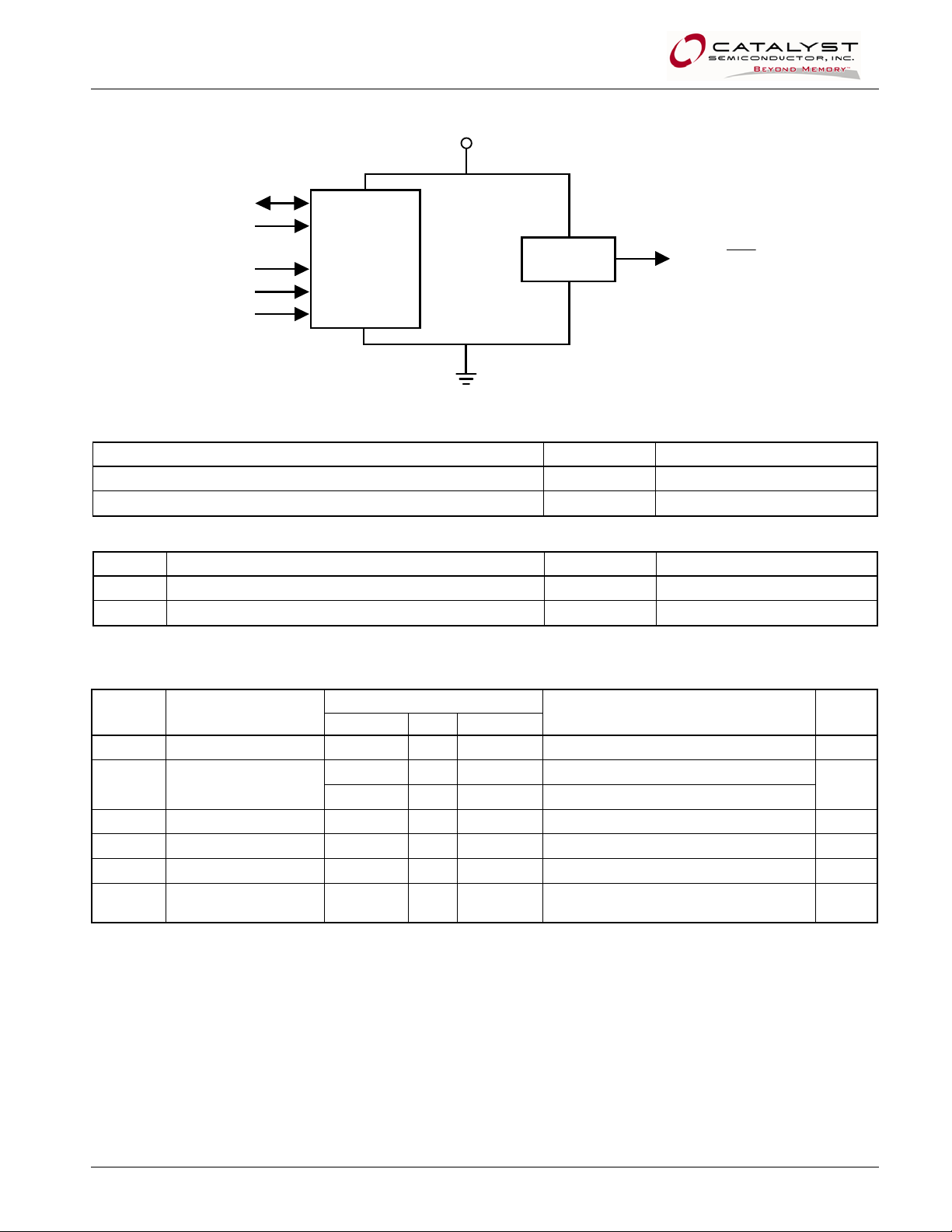
BLOCK DIAGRAM
SDA
SCL
A0
A1
A2
EEPROM
V
CC
V
SS
VOLTAGE
DETECTOR
RST or RS
ABSOLUTE MAXIMUM RATINGS
(1)
Parameters Ratings Units
Storage Temperature -65 to +150 °C
Voltage on Any Pin with Respect to Ground
RELIABILITY CHARACTERISTICS
(3)
(2)
-0.5 to +6.5 V
Symbol Parameter Min Units
(4)
NEND
Endurance 1,000,000 Program/ Erase Cycles
TDR Data Retention 100 Years
D.C. OPERATING CHARACTERISTICS
V
= +2.5V to +5.5V unless otherwise specified.
CC
Limits
Symbol Parameter
Min. Typ. Max.
Test Condition Units
ICC Supply Current 1 Read or Write at 400kHz mA
ISB Standby Current
10 22 V
8 17 V
< 5.5V; All I/O Pins at VSS or VCC
CC
< 3.6V; All I/O Pins at VSS or VCC
CC
IL I/O Pin Leakage 2 Pin at GND or VCC μA
VIL Input Low Voltage -0.5 VCC x 0.3 V
V
VOL Output Low Voltage
Input High Voltage VCC x 0.7 VCC + 0.5 V
IH
SDA
0.4
≥ 2.5 V, IOL = 3.0 mA
V
CC
μA
V
Notes:
(1) Stresses above those listed under “Absolute Maximum Ratings” may cause permanent damage to the device. These are stress ratings
only, and functional operation of the device at these or any other conditions outside of those listed in the operational sections of this
specification is not implied. Exposure to any absolute maximum rating for extended periods may affect device performance and reliability.
(2) The DC input voltage on any pin should not be lower than -0.5 V or higher than V
undershoot to no less than -1.5 V or overshoot to no more than V
(3) These parameters are tested initially and after a design or process change that affects the parameter according to appropriate AEC-Q100
and JEDEC test methods.
(4) Page Mode, V
Doc. No. 1117 Rev. A 2 © 2006 Catalyst Semiconductor, Inc.
= 5 V, 25°C
CC
+ 1.5 V, for periods of less than 20 ns.
CC
+ 0.5 V. During transitions, the voltage on any pin may
CC
Characteristics subject to change without notice
CAT140xx
A.C. CHARACTERISTICS (MEMORY)
V
= 2.5V to 5.5V, TA = -40°C to 85°C, unless otherwise specified.
CC
Symbol Parameter
F
Clock Frequency 100 400 kHz
SCL
t
START Condition Hold Time 4 0.6 µs
HD:STA
t
Low Period of SCL Clock 4.7 1.3 µs
LOW
t
High Period of SCL Clock 4 0.6 µs
HIGH
t
START Condition Setup Time 4.7 0.6 µs
SU:STA
t
Data In Hold Time 0 0 µs
HD:DAT
t
Data In Setup Time 250 100 ns
SU:DAT
(2)
t
SDA and SCL Rise Time 1000 300 ns
R
(2)
t
SDA and SCL Fall Time 300 300 ns
F
t
STOP Condition Setup Time 4 0.6 µs
SU:STO
t
Bus Free Time Between STOP and START 4.7 1.3 µs
BUF
(1)
Standard Fast
Min Max Min Max
Units
tAA SCL Low to Data Out Valid 3.5 0.9 µs
tDH Data Out Hold Time 100 100 ns
(2)
T
Noise Pulse Filtered at SCL and SDA Inputs 100 100 ns
i
tWR Write Cycle Time 5 5 ms
(2, 3)
t
Power-up to Ready Mode 1 1 ms
PU
Notes:
(1) Test conditions according to “A.C. Test Conditions” table.
(2) Tested initially and after a design or process change that affects this parameter.
is the delay between the time VCC is stable and the device is ready to accept commands.
(3) t
PU
A.C. TEST CONDITIONS
Input Levels 0.2 x V
Input Rise and Fall Times
50 ns
≤
to 0.8 x VCC
CC
Input Reference Levels 0.3 x VCC, 0.7 x VCC
Output Reference Levels 0.5 x VCC
Output Load Current Source: IOL = 3 mA; CL = 100 pF
© 2006 Catalyst Semiconductor, Inc. 3 Doc. No. 1117 Rev. A
Characteristics subject to change without notice
CAT140xx
ELECTRICAL CHARACTERISTICS (SUPERVISORY FUNCTION)
V
= Full range, TA = -40ºC to +85ºC unless otherwise noted. Typical values at TA = +25ºC and VCC = 5V for
CC
L/M/J versions, V
Symbol Parameter Threshold Conditions Min Typ Max Units
V
TH
Reset Threshold Voltage
Symbol Parameter Conditions Min Typ
Reset Threshold Tempco 30 ppm/ºC
t
V
RPD
= 3.3V for T/S versions, VCC = 3V for R version and VCC = 2.5V for Z version.
CC
TA = +25ºC 4.56 4.63 4.70
T
= -40ºC to +85ºC 4.50 4.75
A
TA = +25ºC 4.31 4.38 4.45
T
= -40ºC to +85ºC 4.25 4.50
A
TA = +25ºC 3.93 4.00 4.06
T
= -40ºC to +85ºC 3.89 4.10
A
TA = +25ºC 3.04 3.08 3.11
T
= -40ºC to +85ºC 3.00 3.15
A
TA = +25ºC 2.89 2.93 2.96
T
= -40ºC to +85ºC 2.85 3.00
A
TA = +25ºC 2.59 2.63 2.66
T
= -40ºC to +85ºC 2.55 2.70
A
TA = +25ºC 2.28 2.32 2.35
T
= -40ºC to +85ºC 2.25 2.38
A
= VTH to (VTH -100mV) 20 µs
to Reset Delay
CC
L
M
J
T
S
R
Z
(2)
V
CC
(1)
Max Units
V
t
Reset Active Timeout Period TA = -40ºC to +85ºC 140 240 460 ms
PURST
¯¯¯¯¯¯
RESET
Output Voltage Low
(Push-pull, active LOW,
CAT140xx9)
V
OL
¯¯¯¯¯¯
RESET
V
(Push-pull, active LOW,
OH
Output Voltage High
CAT140xx9)
RESET Output Voltage Low
V
OL
(Push-pull, active HIGH,
CAT140xx1)
RESET Output Voltage High
VOH
(Push-pull, active HIGH,
CAT140xx1)
Notes:
(1) Production testing done at T
(2) RESET
output for the CAT140xx9; RESET output for the CAT140xx1.
VCC = VTH min, I
= 1.2 mA
SINK
R/S/T/Z
VCC = VTH min, I
= 3.2 mA
SINK
J/L/M
> 1.0V, I
V
CC
VCC = VTH max, I
= 50µA 0.3
SINK
= -500µA
SOURCE
R/S/T/Z
= VTH max, I
V
CC
SOURCE
= -800µA
J/L/M
VCC > VTH max, I
= 1.2mA
SINK
R/S/T/Z
> VTH max, I
V
CC
= 3.2mA
SINK
J/L/M
1.8V < V
I
SOURCE
= +25ºC; limits over temperature guaranteed by design only.
A
≤ VTH min,
CC
= -150µA
0.3
0.4
0.8V
CC
V
V
- 1.5
V
CC
0.3
V
0.4
0.8VCC V
Doc. No. 1117 Rev. A 4 © 2006 Catalyst Semiconductor, Inc.
Characteristics subject to change without notice
CAT140xx
g
g
N
R
PIN DESCRIPTION
RESET/RESET
This output is available in two versions: CMOS
Active Low (CAT140xx9) and CMOS Active High
(CAT140xx1). Both versions are push-pull outputs
for high efficiency.
SDA: SERIAL DATA ADDRESS
The Serial Data I/O pin receives input data and
transmits data stored in EEPROM. In transmit mode,
this pin is open drain. Data is acquired on the
positive edge, and is delivered on the negative edge
of SCL.
SCL: SERIAL CLOCK
The Serial Clock input pin accepts the Serial Clock
generated by the Master.
A0, A1, A2: Device Address Inputs
The Address inputs set the device address when
cascading multiple devices. When not driven, these
pins are pulled LOW internally.
¯¯¯¯¯¯
: RESET OUTPUT
and remains asserted for at least 140ms (t
PURST
) after
the power supply voltage has risen above the threshold.
Reset output timing is shown in Figure 1.
The CAT140xx devices protect μPs against brownout
failure. Short duration V
transients of 4μsec or less
CC
and 100mV amplitude typically do not generate a Reset
pulse.
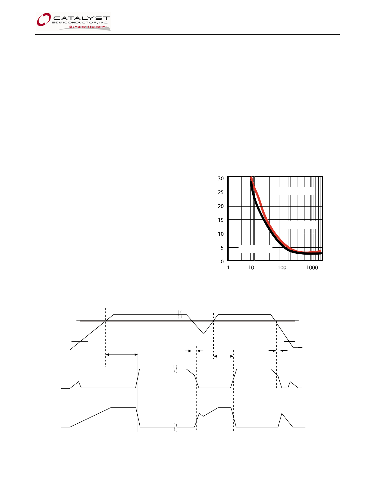
Figure 2 shows the maximum pulse duration of negativegoing V
transients that do not cause a reset condition.
CC
As the amplitude of the transient goes further below the
threshold (increasing V
duration decreases. In this test, the V
- VCC), the maximum pulse
TH
starts from
CC
an initial voltage of 0.5V above the threshold and
drops below it by the amplitude of the overdrive voltage
- VCC).
(V
TH
= 25ºC
T
AMB
ATION [µs]
DEVICE OPERATION
The CAT140xx products combine the accurate
voltage monitoring capabilities of a standalone
voltage supervisor with the high quality and reliability
of standard EEPROMs from Catalyst Semiconductor.
RESET CONTROLLER DESCRIPTION
The reset signal is asserted LOW for the CAT140xx9
and HIGH for the CAT140xx1 when the power
supply voltage falls below the threshold trip voltage
V
CC
V
RVALID
TH
t
PURST
t
RPD
V
RESE T
T DU
CAT140xxZ
CAT1 40xxM
TRANSIE
RESET OVERDRIVE VTH - VCC [mV]
Figure 2. Maximum Transient Duration Without
Causing a Reset Pulse vs. Overdrive Voltage
t
t
PURST
RPD
CAT140xx9
RESE T
ure 1. RESET Output Timin
Fi
CAT140xx1
© 2006 Catalyst Semiconductor, Inc. 5 Doc. No. 1117 Rev. A
Characteristics subject to change without notice

CAT140xx
EMBEDDED EEPROM OPERATION
The CAT140xx supports the Inter-Integrated Circuit
2
C) Bus data transmission protocol, which defines a
(I
device that sends data to the bus as a transmitter and
a device receiving data as a receiver. Data flow is
controlled by a Master device, which generates the
serial clock and all START and STOP conditions. The
CAT140xx acts as a Slave device. Master and Slave
alternate as either transmitter or receiver.
I2C BUS PROTOCOL
The I2C bus consists of two ‘wires’, SCL and SDA.
The two wires are connected to the V
pull-up resistors. Master and Slave devices connect to
the 2-wire bus via their respective SCL and SDA pins.
The transmitting device pulls down the SDA line to
‘transmit’ a ‘0’ and releases it to ‘transmit’ a ‘1’.
Data transfer may be initiated only when the bus is not
busy (see A.C. Characteristics).
During data transfer, the SDA line must remain stable
while the SCL line is HIGH. An SDA transition while
SCL is HIGH will be interpreted as a START or STOP
condition (Figure 3). The START condition precedes
all commands. It consists of a HIGH to LOW transition
on SDA while SCL is HIGH. The START acts as a
‘wake-up’ call to all receivers. Absent a START, a
Slave will not respond to commands. The STOP
condition completes all commands. It consists of a
LOW to HIGH transition on SDA while SCL is HIGH.
START
The START condition precedes all commands.
It consists of a HIGH to LOW transition on SDA while
SCL is HIGH. The START acts as a ‘wake-up’ call to
all receivers. Absent a START, a Slave will not
respond to commands.
supply via
CC
STOP
The STOP condition completes all commands.
It consists of a LOW to HIGH transition on SDA while
SCL is HIGH. The STOP starts the internal Write cycle
(when following a Write command) or sends the
Slave into standby mode (when following a Read
command).
Device Addressing
The Master initiates data transfer by creating a
START condition on the bus. The Master then
broadcasts an 8-bit serial Slave address. For normal
Read/Write operations, the first 4 bits of the Slave
address are fixed at 1010 (Ah). The next 3 bits are
used as programmable address bits when cascading
multiple devices and/or as internal address bits. The
last bit of the slave address, R/W, specifies whether a
Read (1) or Write (0) operation is to be performed.
The 3 address space extension bits are assigned as
illustrated in Figure 4. A
state of the external address pins, and a
, A1 and A0 must match the
2
, a9 and a8
10
are internal address bits.
Acknowledge
After processing the Slave address, the Slave
responds with an acknowledge (ACK) by pulling down
the SDA line during the 9
th
clock cycle (Figure 5). The
Slave will also acknowledge the address byte and
every data byte presented in Write mode. In Read
mode the Slave shifts out a data byte, and then
releases the SDA line during the 9
th
clock cycle. As
long as the Master acknowledges the data, the Slave
will continue transmitting. The Master terminates the
session by not acknowledging the last data byte
(NoACK) and by issuing a STOP condition. Bus timing
is illustrated in Figure 6.
Doc. No. 1117 Rev. A 6 © 2006 Catalyst Semiconductor, Inc.
Characteristics subject to change without notice

Figure 3. START/STOP Conditions
SCL
SDA
CAT140xx
CONDITION
Figure 4. Slave Address Bits
101 0A2A
101 0A2A
101 0A
101 0a
Figure 5. Acknowledge Timing
BUS RELEASE DEL AY (TRANSMITTER) BUS RELEASE DELAY (RECEIVER)
SCL FROM
MASTER
DATA OUTPUT
FROM TRANSMITTER
START
STOP
CONDITION
A0R/W CAT14002
1
a8R/W CAT14004
1
2a9
10a9
189
a8R/W CAT14008
a8R/W CAT14016
DATA OUTPUT
FROM RECEIVER
START
ACK DELAY (≤ tAA)
ACK SETUP (≥ t
SU:DAT
)
Figure 6. Bus Timing
t
AA
t
HIGH
t
HD:DAT
t
LOW
SCL
t
SU:STA
SDA IN
SDA OUT
© 2006 Catalyst Semiconductor, Inc. 7 Doc. No. 1117 Rev. A
Characteristics subject to change without notice
t
F
t
LOW
t
HD:STA
t
DH
t
R
t
SU:DAT
t
SU:STO
t
BUF

CAT140xx
WRITE OPERATIONS
Byte Write
In Byte Write mode, the Master sends the START
condition and the Slave address with the R/W bit set
to zero to the Slave. After the Slave generates an
acknowledge, the Master sends the byte address that
is to be written into the address pointer of the
CAT140xx. After receiving another acknowledge from
the Slave, the Master transmits the data byte to be
written into the addressed memory location. The
CAT140xx device will acknowledge the data byte and
the Master generates the STOP condition, at which
time the device begins its internal Write cycle to
nonvolatile memory (Figure 7). While this internal
cycle is in progress (t
stated and the CAT140xx will not respond to any
request from the Master device (Figure 8).
Page Write
The CAT140xx writes up to 16 bytes of data in a
single write cycle, using the Page Write operation
(Figure 9). The Page Write operation is initiated in the
same manner as the Byte Write operation, however
instead of terminating after the data byte is
transmitted, the Master is allowed to send up to fifteen
additional bytes. After each byte has been transmitted
the CAT140xx will respond with an acknowledge and
internally increments the four low order address bits.
The high order bits that define the page address
remain unchanged. If the Master transmits more than
sixteen bytes prior to sending the STOP condition, the
address counter ‘wraps around’ to the beginning of
page and previously transmitted data will be
overwritten. Once all sixteen bytes are received and
the STOP condition has been sent by the Master, the
internal Write cycle begins. At this point all received
data is written to the CAT140xx in a single write cycle.
), the SDA output will be tri-
WR
Acknowledge Polling
The acknowledge (ACK) polling routine can be used
to take advantage of the typical write cycle time.
Once the stop condition is issued to indicate the end
of the host’s write operation, the CAT140xx initiates
the internal write cycle. The ACK polling can be
initiated immediately. This involves issuing the start
condition followed by the slave address for a write
operation. If the CAT140xx is still busy with the write
operation, NoACK will be returned. If the CAT140xx
has completed the internal write operation, an ACK
will be returned and the host can then proceed with
the next read or write operation.
Doc. No. 1117 Rev. A 8 © 2006 Catalyst Semiconductor, Inc.
Characteristics subject to change without notice

Figure 7. Byte Write Sequence
CAT140xx
BUS ACTIVITY:
MASTER
SLAVE
Figure 8. Write Cycle Timing
SCL
SDA
Byte n
S
T
A
R
T
S
SLAVE
ADDRESS
ACK8th Bit
ADDRESS
A
C
K
STOP
CONDITION
BYTE
a7⎟a
DATA
BYTE
0
d7÷d
0
S
T
O
P
P
A
C
K
ADDRESS
t
WR
A
C
K
START
CONDITION
Figure 9. Page Write Timing
BUS ACTIVITY:
MASTER
SLAVE
S
T
A
R
T
S
n = 1
P ≤ 15
SLAVE
ADDRESS
A
C
K
ADDRESS
BYTE
DATA
BYTE
n
DATA
BYTE
n+1
DATA
BYTE
n+P
S
T
O
P
P
A
C
K
A
C
K
A
C
K
A
C
K
© 2006 Catalyst Semiconductor, Inc. 9 Doc. No. 1117 Rev. A
Characteristics subject to change without notice

CAT140xx
READ OPERATIONS
Immediate Read
Upon receiving a Slave address with the R/W bit set
to ‘1’, the CAT140xx will interpret this as a request for
data residing at the current byte address in memory.
The CAT140xx will acknowledge the Slave address,
will immediately shift out the data residing at the
current address, and will then wait for the Master to
respond. If the Master does not acknowledge the data
(NoACK) and then follows up with a STOP condition
(Figure 10), the CAT140xx returns to Standby mode.
Selective Read
Selective Read operations allow the Master device to
select at random any memory location for a read
operation. The Master device first performs a ‘dummy’
write operation by sending the START condition, slave
address and byte address of the location it wishes to
read. After the CAT140xx acknowledges the byte
address, the Master device resends the START
condition and the slave address, this time with the R/W
bit set to one. The CAT140xx then responds with its
acknowledge and sends the requested data byte. The
Master device does not acknowledge the data (NoACK)
but will generate a STOP condition (Figure 11).
Sequential Read
If during a Read session, the Master acknowledges
st
data byte, then the CAT140xx will continue
the 1
transmitting data residing at subsequent locations until
the Master responds with a NoACK, followed by a
STOP (Figure 12). In contrast to Page Write, during
Sequential Read the address count will automatically
increment to and then wrap-around at end of memory
(rather than end of page).
POWER-ON RESET (POR)
Each CAT140xx incorporates Power-On Reset (POR)
circuitry which protects the internal logic against
powering up in the wrong state.
A CAT140xx device will power up into Standby mode
after V
down into Reset mode when V
exceeds the POR trigger level and will power
CC
drops below the
CC
POR trigger level. This bi-directional POR feature
protects the device against ‘brown-out’ failure follo–
wing a temporary loss of power.
Delivery State
The CAT140xx is shipped erased, i.e., all bytes are FFh.
© 2006 Catalyst Semiconductor, Inc. 10 Doc. No. 1117 Rev. A
Characteristics subject to change without notice

Figure 10. Immediate Read Sequence and Timing
BUS ACTIVITY:
MASTER
S
T
A
R
T
SLAVE
ADDRESS
CAT140xx
N
O
S
T
A
C
O
P
K
P
SCL
S
SLAVE
A
C
K
DATA
BYTE
89
SDA 8th Bit
Figure 11. Selective Read Sequence
BUS ACTIVITY:
MASTER
S
T
A
R
SLAVE
T
ADDRESS
BYTEADDRESS
S
T
A
R
T
SLAVE
ADDRESS
STOPNO ACKDATA OUT
N
O
S
T
A
O
C
P
K
S
SLAVE
Figure 12. Sequential Read Sequence
BUS ACTIVITY:
MASTER
SLAVE
SLAVE
ADDRESS
A
C
K
DATA
BYTE
n
n+x
P
N
O
S
A
T
C
O
K
P
P
S
A
C
K
A
C
K
DATA
BYTE
n+1
A
C
K
A
C
K
DATA
BYTE
n+2
A
C
K
A
C
K
DATA
BYTE
DATA
BYTE
© 2006 Catalyst Semiconductor, Inc. 11 Doc. No. 1117 Rev. A
Characteristics subject to change without notice

CAT140xx
PACKAGE OUTLINES
8-LEAD 150 MIL SOIC (W)
E1
E
D
e
A1
b
SYMBOL
A1
A
b
MIN
0.10
1.35
0.33
NOM
C
D
E
E1
4.80
5.80
3.80
e 1.27 BSC
h
L
0.25
0.40
q1 0° 8°
For current Tape and Reel information, download the PDF file from:
http://www.catsemi.com/documents/tapeandreel.pdf.
Notes:
(1) All dimensions are in millimeters.
(2) Complies with JEDEC specification MS-012 dimensions.
h x 45
C
A
q1
L
MAX
0.25
1.75
0.51
0.250.19
5.00
6.20
4.00
0.50
1.27
Doc. No. 1117 Rev. A 12 © 2006 Catalyst Semiconductor, Inc.
Characteristics subject to change without notice

–
ORDERING INFORMATION
CAT140xx
Prefix
Device # Suffix
CAT 14002 9 S W I
Company ID
Temperature Range
I = Industrial (-40ºC to 85ºC)
Product Type with
Memory Density
02 – 2K-bits
04 – 4K-bits
08 – 8K-bits
16
16K-bits
Reset Threshold Voltage
L: 4.50V – 4.75V
M: 4.25V – 4.50V
J: 3.89V – 4.10V
T: 3.00V – 3.15V
S: 2.85V – 3.00V
R: 2.55V – 2.70V
Z: 2.25V – 2.38V
Package
W: SOIC
- G T3
Lead Finish
G: NiPdAu (PPF)
Tape & Reel
T: Tape & Reel
3: 3000 units / Reel
Supervisor Output Type
9: CMOS Active Low
1: CMOS Active High
Notes:
(1) All packages are RoHS-compliant (Lead-free, Halogen-free).
(2) The standard lead finish is NiPdAu pre-plated (PPF) lead frames.
(3) The device used in the above example is a CAT140029SWI-GT3 (2Kb EEPROM, with Active Low CMOS output, with a reset threshold between
2.85V - 3.00V, in an SOIC, Industrial Temperature, NiPdAu, Tape and Reel.
(4) For additional package and temperature options, please contact your nearest Catalyst Semiconductor Sales office.
© 2006 Catalyst Semiconductor, Inc. 13 Doc. No. 1117 Rev. A
Characteristics subject to change without notice

REVISION HISTORY
Date Rev. Reason
11/09/06 A Initial Issue
Copyrights, Trademarks and Patents
Trademarks and registered trademarks of Catalyst Semiconductor include each of the following:
Beyond Memory™, DPP™, EZDim™, MiniPot™, and Quad-Mode™
Catalyst Semiconductor has been issued U.S. and foreign patents and has patent applications pending that protect its product s.
CATALYST SEMICONDUCTOR MAKES NO WARRANTY, REPRESENTATION OR GUARANTEE, EXPRESS OR IMPLIED, REGARDING THE SUITABILITY OF ITS
PRODUCTS FOR ANY PARTICULAR PURPOSE, NOR THAT THE USE OF ITS PRODUCTS WILL NOT INFRINGE ITS INTELLECTUAL PROPERTY RIGHTS OR THE
RIGHTS OF THIRD PARTIES WITH RESPECT TO ANY PARTICULAR USE OR APPLICATION AND SPECIFICALLY DISCLAIMS ANY AND ALL LIABILITY ARISING
OUT OF ANY SUCH USE OR APPLICATION, INCLUDING BUT NOT LIMITED TO, CONSEQUENTIAL OR INCIDENTAL DAMAGES.
Catalyst Semiconductor products are not designed, intended, or authorized for use as components in systems intended for surgical implant into the body, or other
applications intended to support or sustain life, or for any other application in which the failure of the Catalyst Semiconductor product could create a situation where personal
injury or death may occur.
Catalyst Semiconductor reserves the right to make changes to or discontinue any product or service described herein without notice. Products with data sheets labeled
"Advance Information" or "Preliminary" and other products described herein may not be in production or offered for sale.
Catalyst Semiconductor advises customers to obtain the current version of the relevant product information before placing orders. Circuit diagrams illustrate typical
semiconductor applications and may not be complete.
Catalyst Semiconductor, Inc.
Corporate Headquarters
2975 Stender Way
Santa Clara, CA 95054
Phone: 408.542.1000 Document No: 1117
Fax: 408.542.1200 Revision: A
www.catsemi.com Issue date: 11/09/06
 Loading...