

Page 1
SF-6300(LX-559)
DEC. 1994
(with price)
SF-6300
R
Page 2

CONTENTS
SPECIFICATIONS ..................................................................................................................... 1
SAVING DATA .......................................................................................................................... 4
LSI PIN FUNCTIONS................................................................................................................. 8
TROUBLESHOOTING............................................................................................................. 11
DIAGNOSTICS ........................................................................................................................ 12
SCHEMATIC DIAGRAM.......................................................................................................... 19
ASSEMBLY VIEW ...................................................................................................................22
PARTS LIST ............................................................................................................................ 23
Page 3
SPECIFICATIONS
Display element: 16-column × 4-line LCD
Memory capacity: 64 kB (60972 bytes)
Main component: LSI
Power supply: 2 lithium batteries (CR2025)
Power consumption: 0.05 W
Battery life*:
Approximately 300 hours continuous operation in Telephone Directory
Approximately 250 hours repeating one minute of input and 10 minutes of display in Telephone
Directory
Approximately 12 months for memory backup
Auto power off: Approximately 6 minutes after last key operation
Ambient
temperature range: 0°C ~ 40°C (32°F ~ 104°F)
Dimensions (HWD):
Unfolded: 4.65 x 122 x 146 mm (3/6 x 4 13/16 x 5 3/4 inches)
Folded: 8.9 x 122 x 75 mm (3/8 x 4 13/16 x 2 15/16 inches)
Weight: 91 g (3.2 oz)
Current consumption:
Power Switch Maximum [µA]
OFF 11.0
ON 510
* The batteries that come installed in this unit when you purchase it are for factory test purposes, so
they will probably not provide normal service life.
— 1 —
Page 4
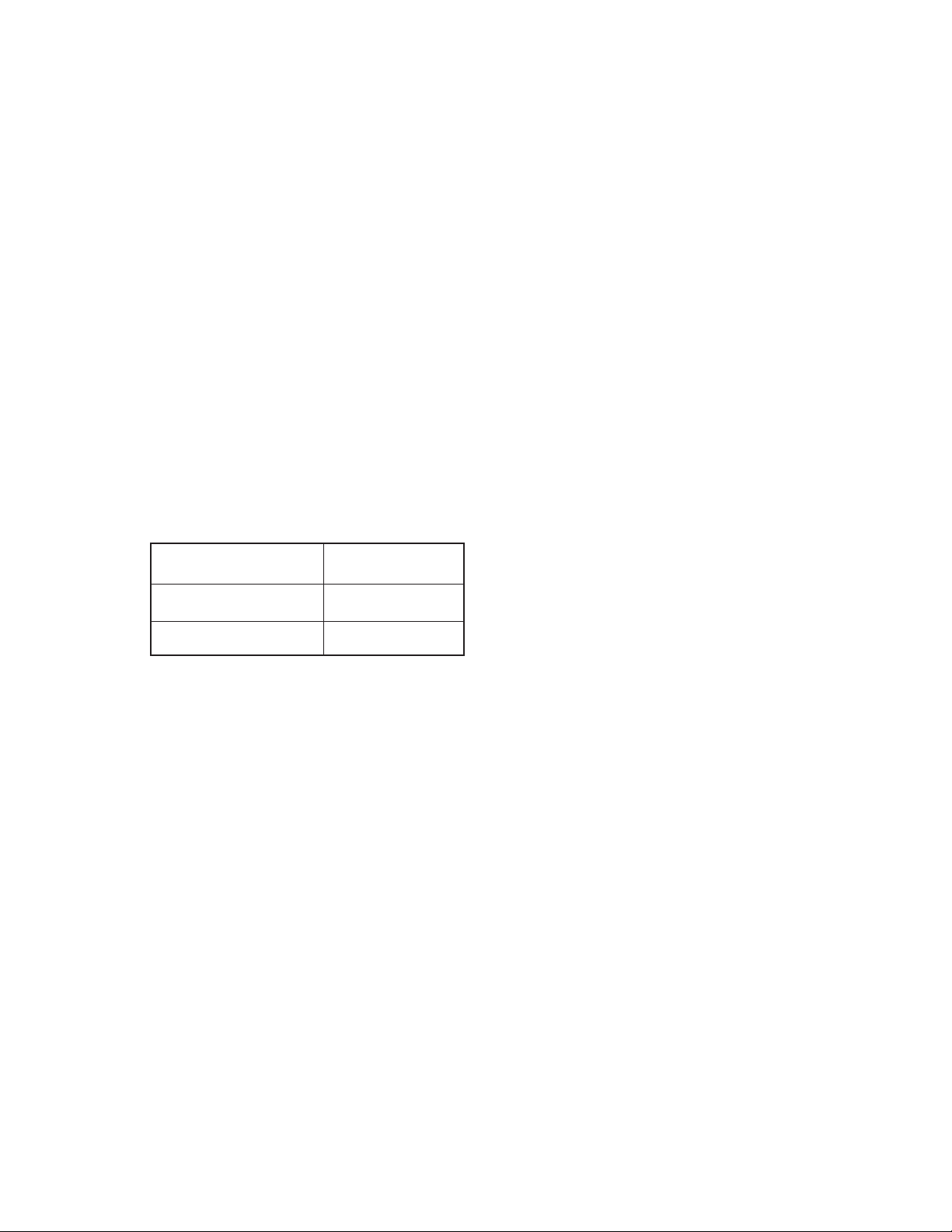
To replace the batteries
1. Loosen the screws on the back of the SF Unit that hold the battery
compartment cover in place, and remove the cover.
• Lift up the edge of the back cover that was fastened down by the
screws, hinging on the opposite edge.
2. Slide the battery switch to the "Replacement" setting.
3. Remove the battery holder by sliding it in the direction indicated by
the arrow in the illustration.
Caution
Be sure to remove only one battery at a time. Otherwise, you will
lose all data stored in memory.
4. Replace the old battery with a new one, making sure that the positive (+) side of the new battery is facing
up (so you can see it).
5. Replace the battery holder and fasten it in place.
6. Repeat steps 2 through 5 for the other battery.
• Be sure to replace both batteries. Never mix old batteries with new
ones, and be sure to use CR2025 lithium batteries only.
7. Slide the battery switch to the "Operational" setting.
8. Replace the back cover of the SF Unit and fasten it in place using
three screws.
• Be careful that you do not over tighten the screws.
— 2 —
Page 5
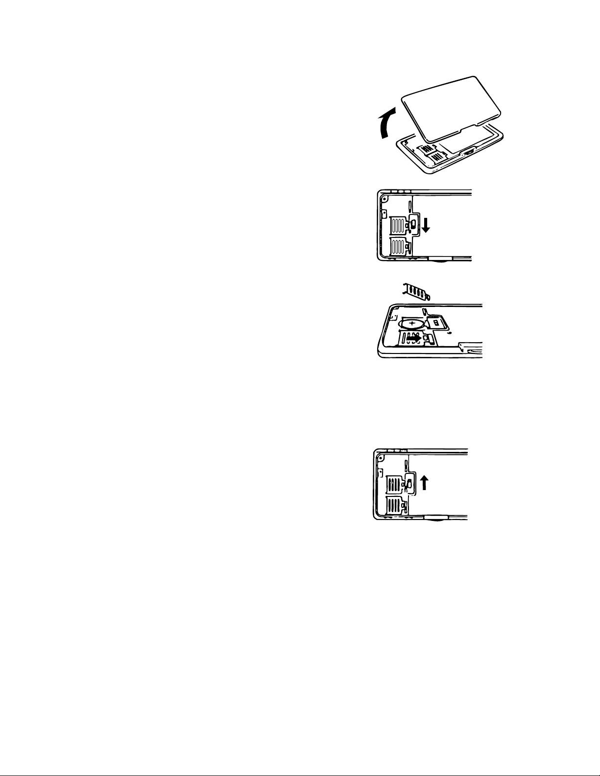
Resetting the SF Unit's Memory
Warning!
The following procedure erases all data stored in the memory of the SF Unit. Perform the following operation
only when you want to delete all data and initialize the settings of the SF Unit.
Remember - you should always keep copies of important data by writing it down, by transferring it to a personal
computer or other SF Unit.
To reset the SF Unit's memory
1. Check to make sure that the power is off.
2. Remove the three screws that hold the back cover in place, and then remove the back cover.
• Lift up the edge of the back cover that was fastened down by the screws, hinging on the opposite edge.
RESET Button
3. Switch on power and press the RESET button with a thin, pointed object. The following message appears
on the display.
ALL DATA
CLEAR!
OK? Y/N
CAPS
4. Press Y* to reset the memory and delete all data or N to abort the reset operation without deleting anything.
* Note that the letter key you press to indicate "yes" depends on the system language, as noted below.
English: Y Spanish: S German: J
French: O Italian: S
5. Replace the back cover and fasten it in place with three screws.
• Be careful that you do not over tighten the screws.
Following the reset operation described above, the Home Time display appears and the SF Unit settings are
initialized as noted below.
Home Time: 12-hour format
JAN/1/1995
AM/12:00 00
Zone: London (LON)
World Time: New York (NYC)
Daily Alarm: 12:00 PM
Language: English
Sound: Schedule alarm ON
Reminder alarm ON
Daily alarm OFF
Key ON
Character input: CAPS
— 3 —
Page 6
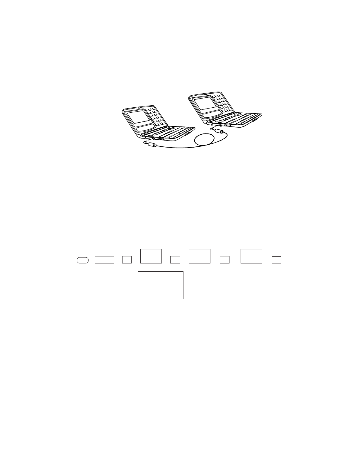
SAVING DATA
The SF-6300 can transfer the customer's data (both the open and secret areas) to another SF-6300.
• Turn off both the transmitting and receiving units and connect them using the SB-60/62 cable.
SB-60/62
1 Setting up the receiving unit:
1. Do the reset operation.
2. Enter the calculator mode. Set the date of receiving unit to February 3rd, 1901.
Operation:
TIME
ON
Note: The customer may have created a password to protect confidential information from
unauthorized access. To be sure this password is transferred to the receiving unit, be sure
to set the date as described above.
CAL
1
DATE
M SUN
1901/ 2/ 3
2
TIME
DATE
TIME
3
DATE
M+
— 4 —
Page 7
3. Press TEL , and FUNC twice.
4. Press 4 to select DATA COMM.
5. Press 2 to select RECEIVE.
1* TO SECRET AREA
2 ALL DELETE
3 LABEL EDIT
4 DATA COMM.
CAPS
1 SEND
2 RECEIVE
3 SET UP PAR.
CAPS
RECEIVE OK
DATA
TO STOP
PRESS (ESC)
CAPS
*If the password isn't
registered in the SF-6300,
the display shows X instead
of "1."
— 5 —
Page 8

2 Setting up the transmitting unit:
Set the hardware parameters as follows:
Parity: None Bit length: 7 BPS: 9600
1. Press , .
2. Press twice.
ON
FUNC
TEL
1* TO SECRET AREA
2 ALL DELETE
3 LABEL EDIT
4 DATA COMM
3. Press to select DATA COMM.
4
1 SEND
2 RECEIVE
3 SET UP PAR.
4. Press to select SET UP.
3
*If the password isn't
registered in the SF-6300,
the display shows X instead
of "1."
CAPS
CAPS
✻✻ SET UP PAR. ✻✻✻
PARITY E O N
BIT LENGTH 7 8
BPS 4800 9600
CAPS
5. Use , , , or to select "N," "7," and "9600" and press SET .
1 SEND
2 RECEIVE
3 SET UP
CAPS
— 6 —
Page 9

6. Press 1 to select SEND.
1 ONE ITEM
2 MODE DATA
3 ALL DATA
- SEND -
CAPS
7. Press 3 to select ALL DATA.
SEND ALL DATA?
SET/ESC
CAPS
8. Press SET to start data transmission or ESC to abort the operation without sending
anything.
SENDING
DATA
TO STOP
PRESS (ESC)
CAPS
• If an error occurs during data transmission, the message “TRANSMIT ERROR!” appears on the display.
Press ESC to clear the error message.
9. After data transmission is complete, the display returns to the initial screen of the telephone mode.
— 7 —
Page 10

LSI PIN FUNCTIONS
CPU: LSI1
No.1
Pin No. Name I/O Description
1 ~ 5 C0 ~ 4 Out Common signal for display
6 GND In GND 0 V
7,8 BZ1,2 Out Buzzer terminal
9 VDD In Power supply terminal (+5.3 V)
10 CSRA1 Out Chip enable signal for LSI2
11 CSRA2 Out Chip enable signal for LSI3
12 CSROM Out Chip enable signal (Not used)
13 WEB Out Write enable signal for LSI2 and LSI3
14,15 RA15,16 Out Address bus (Not used)
16 ~ 30 A0 ~ 14 Out Address bus
31 ~ 38 IO0 ~ 7 I/O Data bus
39 ~ 54 KY0 ~ 15 I/O Key signal
55 SW In Battery switch Power on: 0 V off: 6 V
56 DEBUG - Not used
57 ON Out Data communication enable signal
58 CRCKI In GND 0 V
59 SOUTB Out Transmission data output
60 SIN In Receiving data input
61 VDD In Power supply terminal (+5.3 V)
62 TEST - Not used
63 VTM - Not used
— 8 —
Page 11

Pin No. Name I/O Description
64,65 OSC I/O I/O Clock terminal
67,69~71 V1 ~ 4 Voltage for LCD drive
OFF: 0 V ON–V1: 0.64 Minimum ~ 1.29 Maximum V
V2: 1.29 Minimum ~ 2.56 Maximum V
V3: 3.99 Minimum ~ 2.71 Maximum V
V4: 4.64 Minimum ~ 3.99 Maximum V
68 NC - Not used
72 INTO In Low battery detection INTO < 5.2 V => No power on
73 STNT - GND 0 V
74 VLCD In Power supply terminal (+5.3 V)
75 ~ 171
172 ~199
168,200 NC - Not used
RAM: LSI2 and LSI3 (CXK58257)
S0 ~ 95 Out Segment signal for display
C5 ~ 32 Out Common signal for display
22
OE–
23
A11
24
A9
25
A8
26
A13
27
WE–
28
VCC
1
A14
2
A12
3
A7
4
A6
5
A5
6
A4
7
A3
Pin No. Name I/O Description
1~10,21,23~26 A0 ~ 14 In Address bus
11~13,15~19 IO1 ~ IO8 I/O Data bus
14 GND In GND 0 V
20 CE In Chip select signal from LSI1
22 OE In 0 V
27 WE In Write enable signal from LSI1
28 VCC In Power supply terminal (+ 5.3 V)
(LSI 2)
CXK58257ATM
A10
CE–
IO8
IO7
IO6
IO5
IO4
GND
IO3
IO2
IO1
A0
A1
A2
21
20
19
18
17
16
15
14
13
12
11
10
9
8
— 9 —
Page 12

VOLTAGE REGULATOR: REG1 (S-81253)
Output Voltage (VDD): 5.3 V ± 5%
VCC
GND
2
+
–
REF
V
1
VOLTAGE DETECTOR: DET1 (RH5VL46CA)
VCC
2
1
R
R
OUT
A
B
3
VDD
R
I
1
GND2VCC
3
VDD
1
2
OUT
VCC3GND
3
GND
Input Voltage (VCC) Output Voltage (OUT)
VCC > 5.2 V 5.2 V
VCC < 5.2 V 0 V
— 10 —
Page 13

TROUBLESHOOTING
Before the following solutions will be done, save data if possible.
SYMTOM
No Power
No display at all or wrong
display
No key input at all
CAUSE
Battery shortage
Poor soldering of the power supply
circuit
Defective LSI-1 or LSI-2
Defective Capacitor C8, C12, C13, or
C14
Defective TAB LSI
Defective heat seal
Defective LCD
Poor soldering LSI-1 or LSI2
Defective LSI-1 or LSI-2
SOLUTION
Replace batteries
Resolder
Replace it
Replace it
Replace it
Replace it
Replace it
Resolder
Replace it
— 11 —
Page 14

DIAGNOSTICS
Notes: 1. Be sure to transfer data to another SF-6300 unit before entering
the diagnostic mode, because the data will be changed by entering
the diagnostic mode.
2. The check pads shown in the following illustration are covered by a
blind label.
Check Pads
3. To exit the diagnostic mode, press the reset button.
To enter the diagnostic mode:
Blind label
1. Slide the battery switch to "Replacement" position.
2. Slide it to "Operational" position while shorting the check pads.
SELF TEST PROG.
PRESS SEARCH
QUIT BY OFF
CASIO APR 1994
3. Press .
SEARCH
TEST 2 MEMORY
MENU 3 KEY
4 BUZZER
1 DISP 5 I/F
— 12 —
Page 15

Display Check
Operation Display Note
Press 1 on the TEST MENU.
1
2
DISP 4 RVS.
1 WHITE 5 FRAME
2 BLACK 6 DOT4
3 CHECK. 7 TIME
Display check
To return to the
TEST MENU,
ESC
press .
No display
All dots displayed
4
5
3
ACC CAPS SHIFT
,
Checker displayed
SEARCH
Reverse checker
display
Frame display
— 13 —
Page 16

Operation Display Note
6
TIME DISPLAY
7
00:00:XX
ESC
TEST 2 MEMORY
MENU 3 KEY
4 BUZZER
1 DISP 5 EXT
Memory Check
The functions of the numbered items on the display include:
Shows dots at
corners.
Check to see if
timer is working.
1. WR1 :Writes the test pattern in the ROM to the RAM area. (Test pattern: Incremental order 00,
01, and so on)
2. READ1 :Compares the test pattern with the write data (WRITE1) of the RAM and displays the
results.
3. WR2 :Writes the test pattern in the ROM to the RAM area. (Test pattern: Decremental order
FF, FE, and so on)
4. READ2 :Compares the test pattern with the write data (WRITE2) of the RAM and displays the
results.
5. DUMP :Dump the data stored in ROM.
6. CHKSUM :Calculate SUM and XOR of RAM connected and display them.
Operation Display Note
2
1
( or 3 )
MEMORY 3 WR2
4 READ2
1 WR1 5 DUMP
2 READ1 6 CHKSUM
WRITE1
( or WRITE2 )
RAM check
To return to the
TEST MENU,
press .
ESC
5: Not used
6: Not used
— 14 —
Page 17

Operation Display Note
(After a few seconds)
2
( or 4 )
MEMORY 3 WR2
4 READ2
1 WR1 5 DUMP
2 READ1 6 CHKSUM
EXECUTING!!
COMPLETE!!
64KB
DATA ERROR!!
ADDRESS CORR RAM
XXXX XX XX
RAM error
If the displayed address
is within 0000-7FFF,
check LSI3.
If the displayed address
is within 8000-FFFF,
check LSI2.
5
6
07 B5 C7 0B FF
D6 88 20 03 EB
83 47 F7 1B 81
86 82
(E.G.)
TY SZ SUM XOR
FE 0 128 E290 XX
C3 A 64 XXXX XX
(Value: Address).
07: 00001
B5: 00002
C7: 00004
0B: 00008
FF: 00010
D6: 00020
88: 00040
20: 00080
03: 00100
EB: 00200
83: 00400
47: 00800
F7: 01000
1B: 02000
81: 04000
86: 08000
82: 10000
(E.G.)
— 15 —
Page 18

Key Check
Each key has its own key code. The key codes are assigned incrementally from left to right on the keyboard.
(Refer to the keyboard in the schematic diagrams.)
In the auto mode, the key input sequence is limited so that the keys must be pressed in the order of the key
code as mentioned above. If a key is pressed in the wrong order, the SF-6300 beeps.
Operation Display Note
Press 3 on the TEST MENU.
2
MC MR M– M+
AC , ... % 7 , ... ÷
4 , ... x 1 , ... –
0 , ... + ON OFF
EXPENSE , ... DISP CHNG
REMINDER , ... DEL
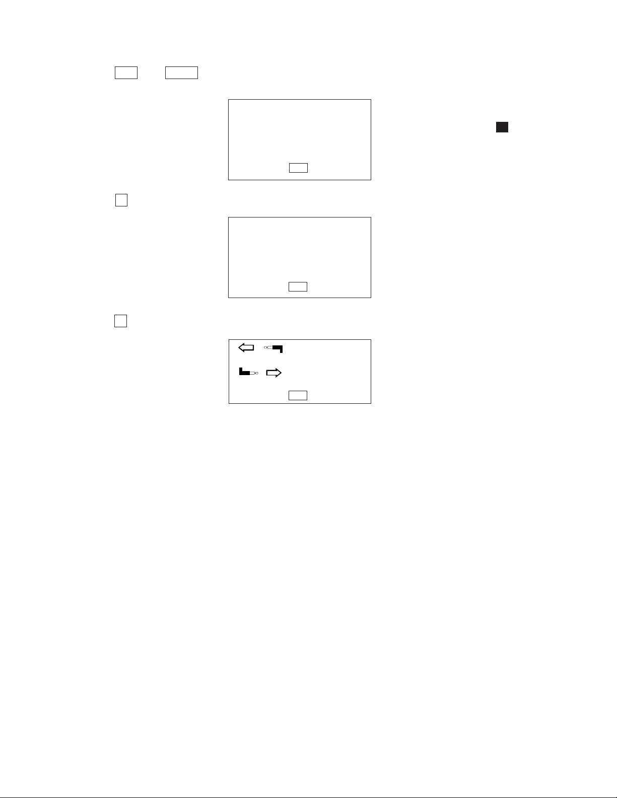
← ↑ ↓ → ESC , ... ( )
FUNCTION , ... SHIFT , ...
SHIFT CAPS , ... SET
SEARCH
KEY 1 RANDOM
2 AUTO
No display
00 01 02 03 04 ...............
............... 56 57
TEST 2 MEMORY
MENU 3 KEY
4 BUZZER
1 DISP 5 EXT
Key check
To return to the TEST
MENU, press ESC .
Check that the key
number appears on
the display.
To return to the TEST
MENU, enter
SEARCH .
— 16 —
Page 19

Buzzer Check
Operation Display Note
Press 4 on the TEST MENU.
1
( or 2 , 3 )
ESC
BUZZER 1 BEEP
2 ALARM1
3 ALARM2
EXECUTING!!
BUZZER 1 BEEP
2 ALARM1
3 ALARM2
TEST 2 MEMORY
MENU 3 KEY
4 BUZZER
1 DISP 5 EXT
Buzzer check
To return to the
TEST MENU,
press .
ESC
Check the sound.
To return to the
BUZZER menu,
press any key.
— 17 —
Page 20

SCHEMATIC DIAGRAM
Main PCB
— 18 —
Page 21

Key PCB
— 19 —
Page 22

Key PCB (Display Side)
— 20 —
Page 23

ASSEMBLY VIEW
1
2
33
3
34
17
4
19
5
18
20
35
36
6
26
37
7
21
8
22
25
9
23
38
39
40
41
10
11
12
13
14
15
16
28
27
24
30
29
32
11
11
31
42
22
23
25
43
44
45
46
47
— 21 —
Page 24

AM : STANDARD (Black)
PARTS LIST BM :
N Item Code No. Parts Name Specification M N.R.Yen R
L559-1 PCB ASS'Y
N C9 2895 1967 Tantalum capacitor ECST1CX106R
C10 2845 1540 Chip capacitor MCH212F104ZK
C11 2895 1967 Tantalum capacitor ECST1CX106R
N CN1 3501 9191 Connector 52746-3090
D1 2390 2128 Chip diode MA740-(TX)
D2 2390 0364 Schottky diode MA713-TX
DET1 2105 3864 CMOS IC RH5VL46CA-T1
N JC1 3501 8778 Mini jack HSJ1563-010010
N Q1 2259 0959 Chip digital transistor DTC114YKT-146
R5 2792 1191 Chip resistor MCR10EZHJ182
R6 2792 0462 Chip resistor MCR10EZHJ473
R7 2792 0470 Chip resistor MCR10EZHJ102
R8 2792 0217 Chip resistor MCR10EZHJ101
R9 2792 0217 Chip resistor MCR10EZHJ101
N REG1 2105 3290 CMOS IC S-81253SGUP-DIJ-T1
19 7435 9096 Buzzer EFB-S55C42AP4
36 6408 9410 Battery contact spring B C311911-2
N 37 6409 9960 Battery contact spring A C413299-1
N 38 6409 9970 Tape A-L525AM C413327-1
L559-E2 PCB ASS'Y 578
C1 2845 1540 Chip capacitor MCH212F104ZK
C2 2845 1540 Chip capacitor MCH212F104ZK
C3 2845 1540 Chip capacitor MCH212F104ZK
C4 2845 1540 Chip capacitor MCH212F104ZK
C5 2845 1652 Chip capacitor MCH215A180JK
C6 2845 1652 Chip capacitor MCH215A180JK
C7 2845 1540 Chip capacitor MCH212F104ZK
C8 2845 1540 Chip capacitor MCH212F104ZK
C12 2845 1540 Chip capacitor MCH212F104ZK
C13 2845 1540 Chip capacitor MCH212F104ZK
C14 2845 1540 Chip capacitor MCH212F104ZK
LSI1 6409 2760 L594 TAB sub ass'y C312133*1
LSI2 2011 8267 LSI CXK58257ATM-10/12L
LSI3 2011 8274 LSI CXK58257AYM-10/12L
LSI4 2011 9268 LSI uPD23C1001EAGZ-M05
R3 2795 0056 Chip resistor MCR10EZHJ000
R11 2792 0209 Chip resistor MCR10EZHJ104
R12 2797 1288 Chip resistor ERJ-6GEYK106V
X1 7110 0642 Crystal oscillator DT-26S
CABINET 2,648
N 1 6412 4330 Lower panel A-L559AM C211663-1
N 1 6412 4480 Lower panel A-L559BM C211663-2
N 2 6412 4310 Earth spring L559AM C413749-1
N 3 6412 4280 Tape E-L559AM C413743-1
N 4 6412 4110 Lower cabinet A-L559AM C111382-1
N 5 6412 4290 W tape D-L559AM C413744-1
N 6 5610 8230 Heat seal P-L559AM C413738-1
N 7 6412 4260 Tape P-L559AM C413741-1
N 8 4311 9180 PCB-L559-KY C211650-1
N 9 6412 4030 L559-E2 PCB ass'y C211666C*1A
Notes: N – New parts R – A : Essential
M – Minimum order/supply quantity B : Stock recommended
R – Rank C : Others
Q'ty
BM AM Unit Price
1
1
1
1
1
1
1
1
1
1
1
1
1
1
1
1
2
2
1
1
1
1
1
1
1
1
1
1
1
1
1
1
1
1
1
1
1
1
0
1
1
1
1
1
1
1
1
1
X : No stock recommended
B.O.S.S. (Black)
FOB Japan
110 39 C
120 4 C
1 1 39 C
1 5 98 C
1 5 50 C
110 33 C
110 45 B
1 5 59 C
120 12 C
110 9 C
120 3 C
120 3 C
120 3 C
120 3 C
1 5 60 B
1 5 55 X
220 6 X
220 26 X
110 31 X
120 4 C
120 4 C
120 4 C
120 4 C
120 3 C
120 3 C
120 4 C
120 4 C
120 4 C
120 4 C
120 4 C
1 1 1,010 B
1 1 580 B
1 1 580 B
1 1 370 B
120 3 C
120 3 C
120 3 C
110 57 B
1 1 830 X
0 1 830 X
120 10 X
120 23 X
1 1 120 X
120 10 X
110 36 B
120 10 X
1 1 140 X
1 1 4,720 X
— 23 —
Page 25

FOB Japan
N Item Code No. Parts Name Specification M N.R.Yen R
N 10 6412 4180 Spacer L559AM C312382-1
N 11 6409 9950 Screw 1A-L525AM A310609-11
N 12 6412 4240 W tape LC-559AM C413739-1
13 3335 5264 LCD CD792-TS
N 14 6412 4250 Tape L-L559AM C413740-1
N 15 5610 8220 Heat seal L-L559AM C312396-1
N 16 6412 4200 Upper sheet A-L559AM C312391-1
N 16 6412 4390 Upper sheet A-L559BM C312391-2
N 17 6410 0080 Hinge L525BM C312119-2
N 18 6410 0210 Tape HB-L525AM C413323-1
20 6512 5920 Buzzer tape L571AM C412699-1
N 21 6410 0160 Earth spring L525AM C413294-1
22 6512 5880 P spring blind L571AM C411700-2
23 6408 9460 Nut L594AM C413032-2
N 24 6412 4210 FFC joiner L559AM C312397-1
N 25 6409 9900 Pin L525AM C413298-1
N 26 6410 0170 Rubber key L525AM C311028-3
N 27 6410 0140 Cap L525AM C312138-1
N 28 6412 4190 VR blind L559AM C312383-1
N 29 6412 4270 Tape HA-L559AM C413742-1
N 30 6410 0130 OP knob L525AM C312114-1
N 31 6412 4220 AN tape L559AM C413734-1
N 32 6412 4160 Tape B-L559AM C312126-2
N 33 6412 4130 Upper sheet B-L559AM C211669-1
N 34 6409 9950 Screw 1A-L525AM A310609-11
N 35 6412 4070 L559-1 PCB ass'y C240001*1
N 39 6412 4300 B blind L559AM C413745-1
N 40 6412 4320 Tape BC-L559AM C440004-1
N 41 6410 0150 Contact spring L525AM C412167-2
N 42 6410 0120 SW knob L525AM C211441-1
N 43 6410 0110 Lower cabinet B-L525BM C111233-2
N 44 6409 9930 Tape C-L525AM C413333-1
N 45 6409 9890 Battery holder L525AM C413296-1
N 46 6412 4120 Lower panel B-L559AM C211439-3
N 46 6412 4370 Lower panel B-L559BM C211439-4
N 47 6411 3100 Screw A-L529AA C413301-2
Q'ty
BM AM Unit Price
110 36 C
1
720 7 X
7
220 10 X
2
1 1 790 B
1
120 13 X
1
1 1 190 B
1
1 1 160 A
0
0 1 160 A
1
110 39 X
1
120 8 X
1
120 17 X
1
120 13 X
1
320 9 X
3
310 35 X
3
1 1 180 X
1
220 27 X
2
110 28 X
1
120 19 X
1
110 28 X
1
120 10 X
1
1 5 57 X
1
1 5 57 X
1
110 36 X
0
1 1 150 A
1
11 20 7 X
11
1 1 1,300 C
1
120 16 X
1
110 25 X
1
120 13 X
1
110 49 X
1
1 5 95 X
1
220 16 X
2
220 37 X
2
1 1 470 X
0
0 1 470 X
1
320 2 X
3
Notes: N – New parts R – A : Essential
M – Minimum order/supply quantity B : Stock recommended
R – Rank C : Others
— 24 —
X : No stock recommended
Page 26

MA0200751A
 Loading...