

Page 1
SF-5300B(LX-547)
SEP. 1994
(with price)
SF-5300B
R
Page 2

CONTENTS
1. SCHEMATIC DIAGRAM
1-1. MAIN PCB..................................................................................................................1
1-2. KEY MATRIX 1 ..........................................................................................................2
1-3. KEY MATRIX 2 ..........................................................................................................3
2. SPECIFICATIONS ............................................................................................................5
3. REPLACING THE BATTERIES ........................................................................................6
4. RESETTING THE UNIT ....................................................................................................7
5. SAVING DATA..................................................................................................................8
6. LSI PIN FUNCTIONS
6-1. CPU:LSI1 .................................................................................................................12
6-2. RAM:LSI2 AND LSI3 (CXK58257) ..........................................................................13
6-3. VOLTAGE REGULATOR:REG1 (S-81253) ............................................................14
6-4. VOLTAGE DETECTOR:DET1 (RH5VL46CA) ........................................................14
7. TROUBLESHOOTING ....................................................................................................15
8. DIAGNOSTICS................................................................................................................18
9. ASSEMBLY VIEW ..........................................................................................................23
10. PARTS LIST....................................................................................................................25
Page 3
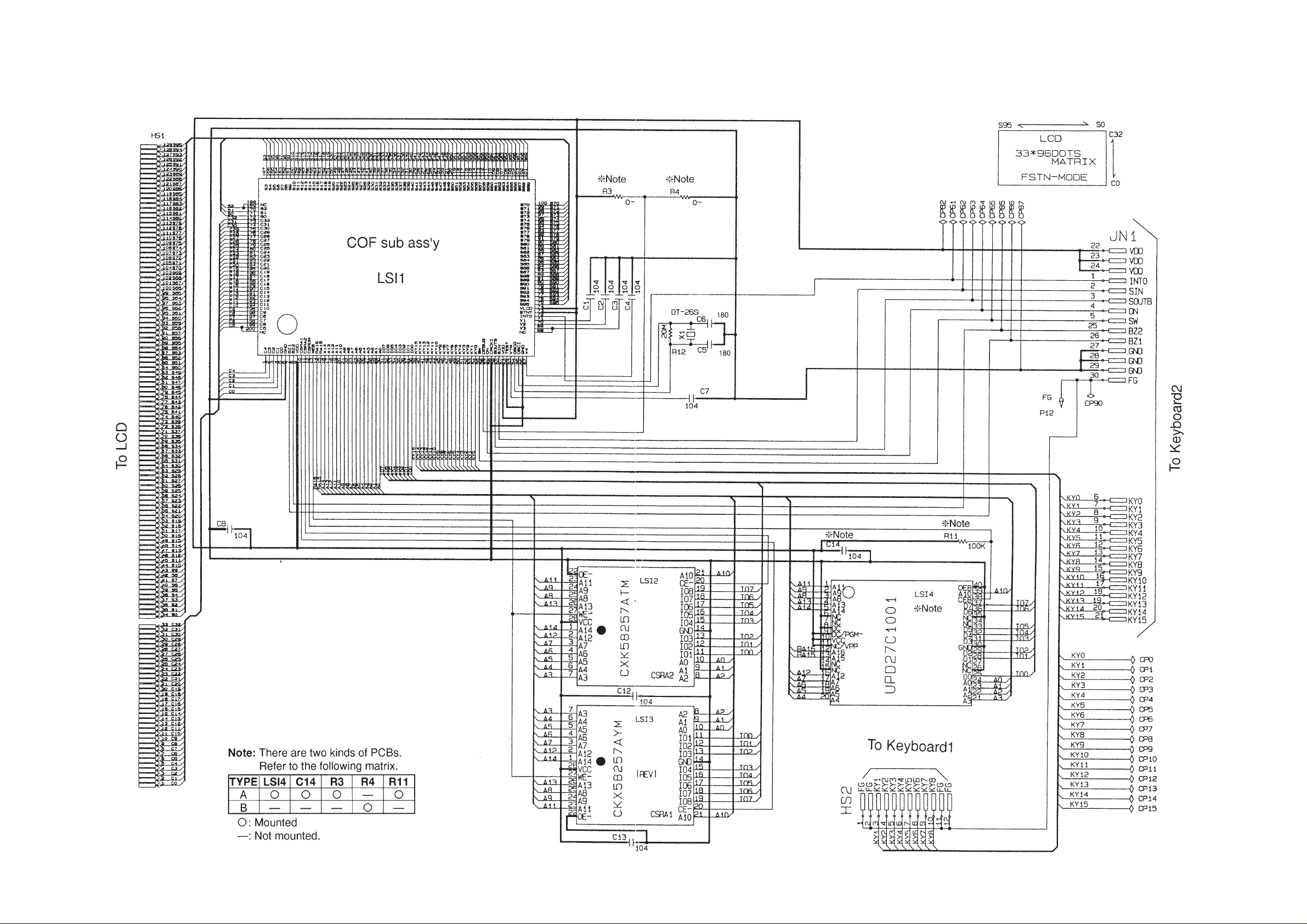
1. SCHEMATIC DIAGRAM
1-1. MAIN PCB
— 1 —
Page 4
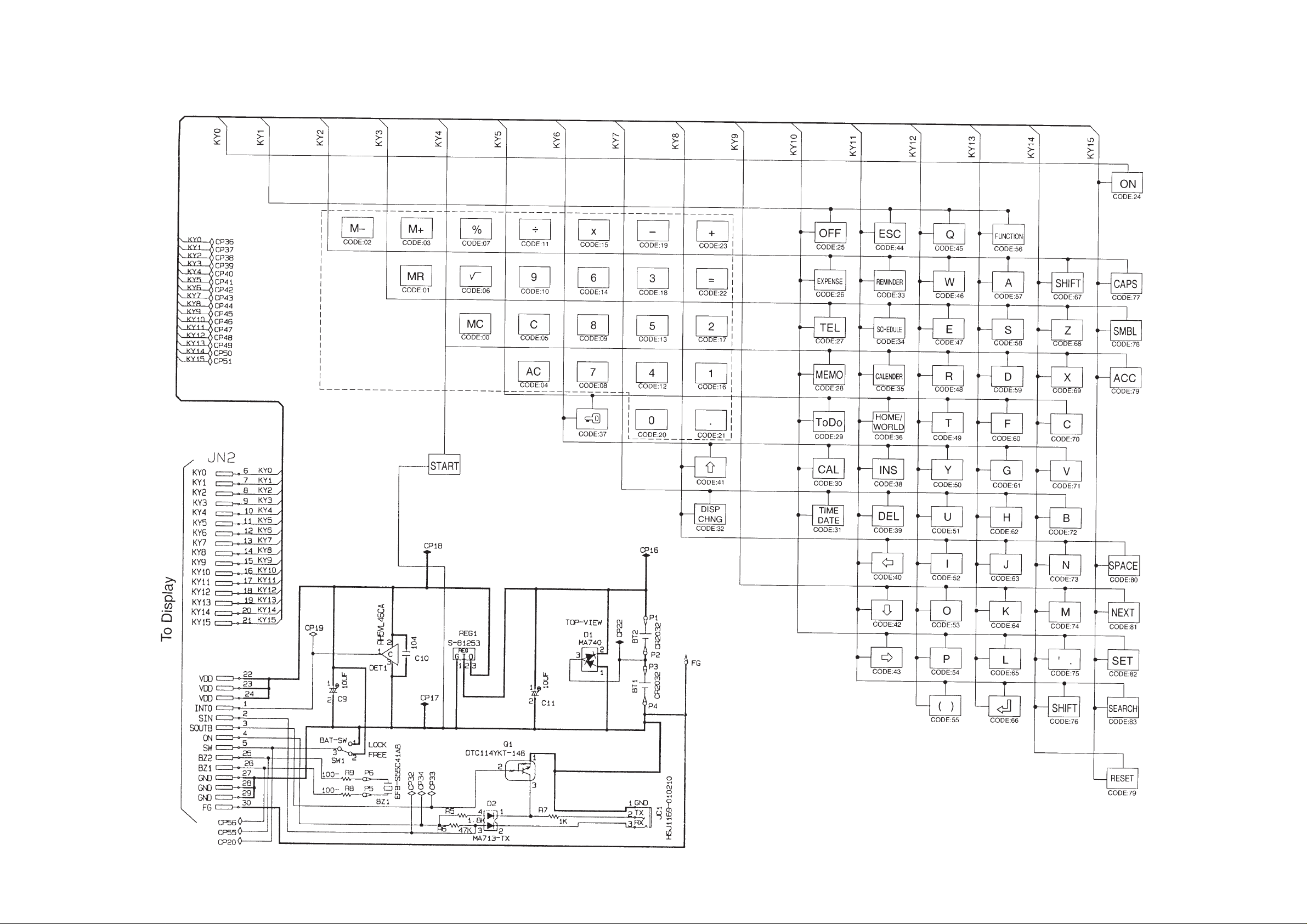
1-2. KEY MATRIX 1
— 2 —
Page 5
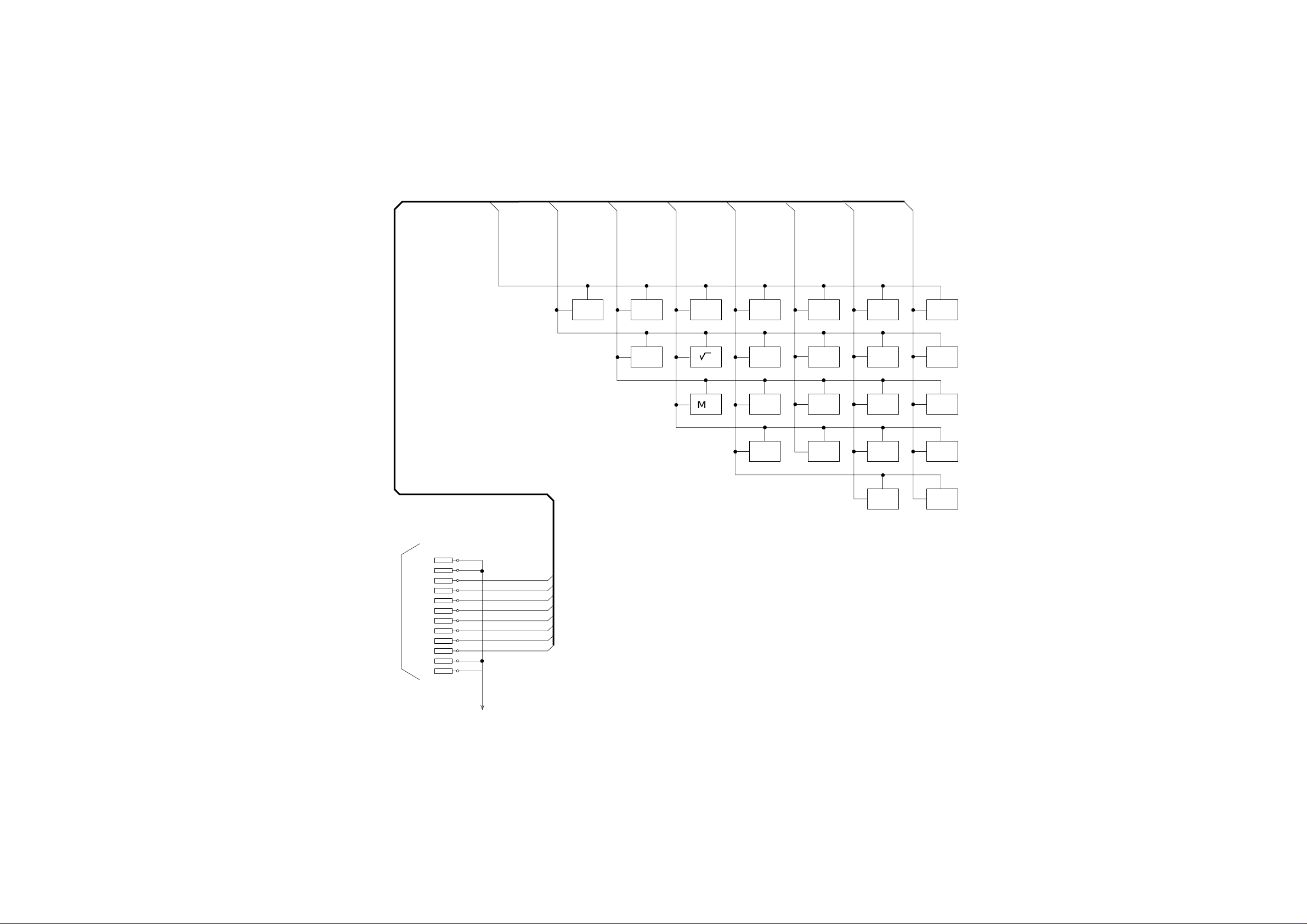
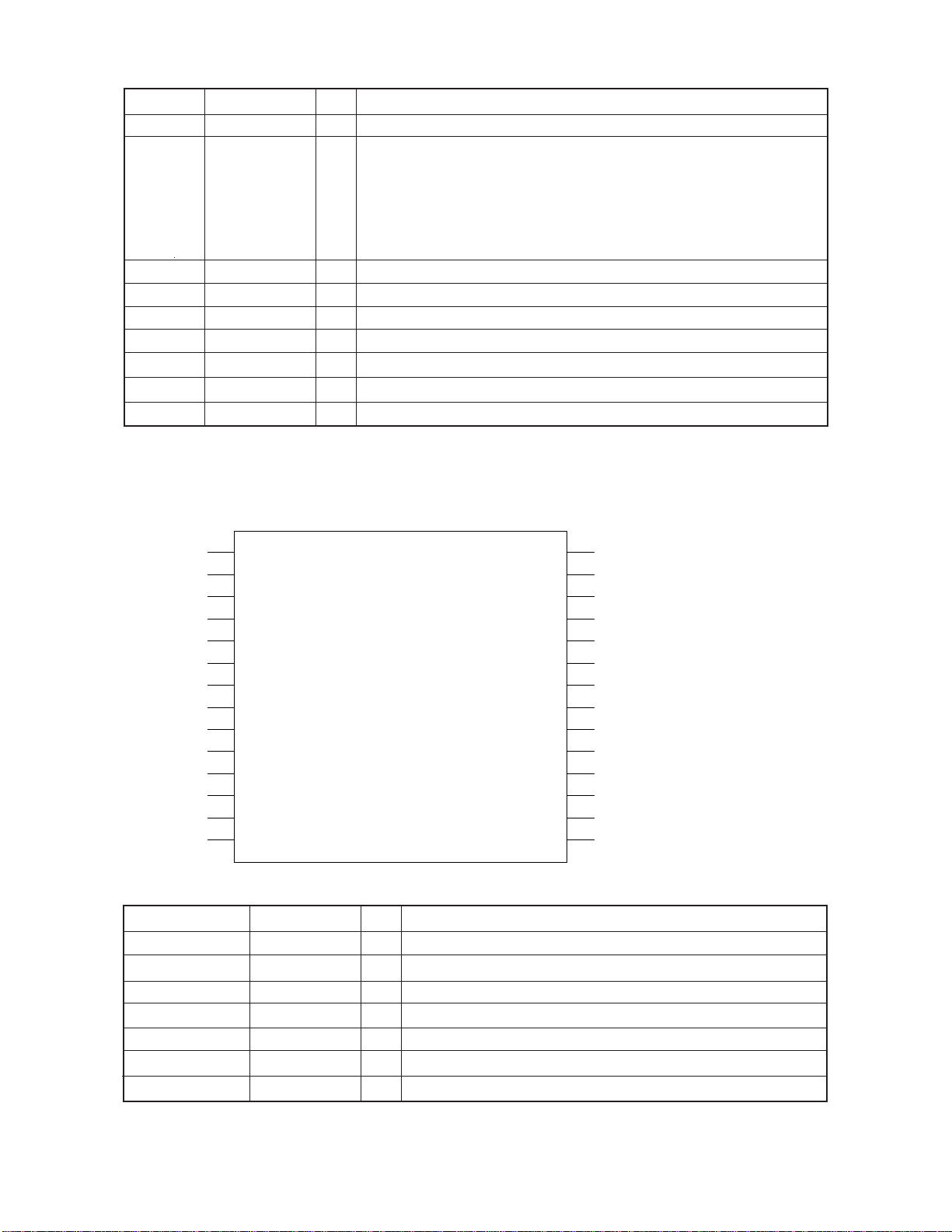
1-3. KEY MATRIX 2
HS3
FG
FG
KY1
KY2
KY3
KY4
KY5
KY6
KY7
To Display
KY8
FG
FG
1
2
3
4
5
6
7
8
9
10
11
12
KY1
KY1
KY2
KY3
KY4
KY5
KY6
KY7
KY8
KY2
M– M+
KY3
CODE:03CODE:02
MR
CODE:01
KY4
%
CODE:07
'
CODE:06
MC
CODE:00
KY5
÷
CODE:11
9
CODE:10
C
CODE:05
AC
CODE:04
KY6
x
CODE:15
6
CODE:14
8
CODE:09
7
CODE:08
KY7
–
CODE:19
3
CODE:18
5
CODE:13
4
CODE:12
0
CODE:20
KY8
+
CODE:23
=
CODE:22
2
CODE:17
1
CODE:16
.
CODE:21
FG
— 3 —
Page 6
2. SPECIFICATIONS
Display element: 16-column × 4-line LCD
Memory capacity: 64 kB (60972 bytes)
Main component: LSI
Power supply: 2 lithium batteries (CR2032)
Power consumption: 0.05 W
Battery life:
Approximately 400 hours continuous operation in Telephone Directory
Approximately 350 hours repeating one minute of input and 10 minutes of display in Telephone
Directory
Approximately 12 months for memory backup
Auto power off: Approximately 6 minutes after last key operation
Ambient
temperature range: 0°C ~ 40°C (32°F ~ 104°F)
Dimensions (HWD):
Unfolded: 8.4 x 139 x 148 mm (3/8 x 5 1/2 x 5 7/8 inches)
Folded: 15.8 x 139 x 74 mm (5/8 x 5 1/2 x 2 7/8 inches)
Weight: 98.2 g (3.5 oz)
Current consumption:
Power Switch Maximum [µA]
OFF 11.0
ON 510
— 5 —
Page 7
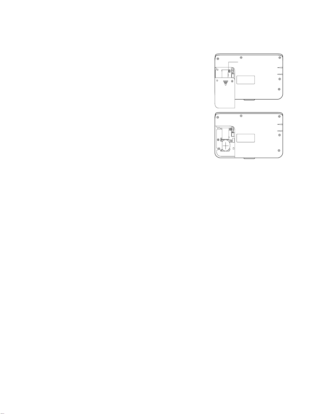
3. REPLACING THE BATTERIES
1. Loosen the screw on the back of the SF-5300B that
holds the battery compartment cover in place, and
remove the cover.
2. Loosen the screw that secures one of the two battery
holders in place and remove the battery holder.
Caution:Be sure to remove only one battery at a time.
Otherwise, you will lose all data stored in memory.
3. Replace the old battery with a new one. Be sure that
the positive (+) side of the new battery is facing up (so
you can see it).
4. Replace the battery holder and secure it by tightening its screw.
• Be careful that you do not overtighten the screw.
5. Repeat Steps 2 through 4 for the other battery.
• Be sure to replace both batteries. Never mix old batteries with new ones, and be sure to use
CR2032 lithium batteries only.
Screw
RESET
6. After you replace both batteries, replace the battery compartment cover and secure it by tightening
its screw.
• Be careful that you do not overtighten the screw.
— 6 —
Page 8
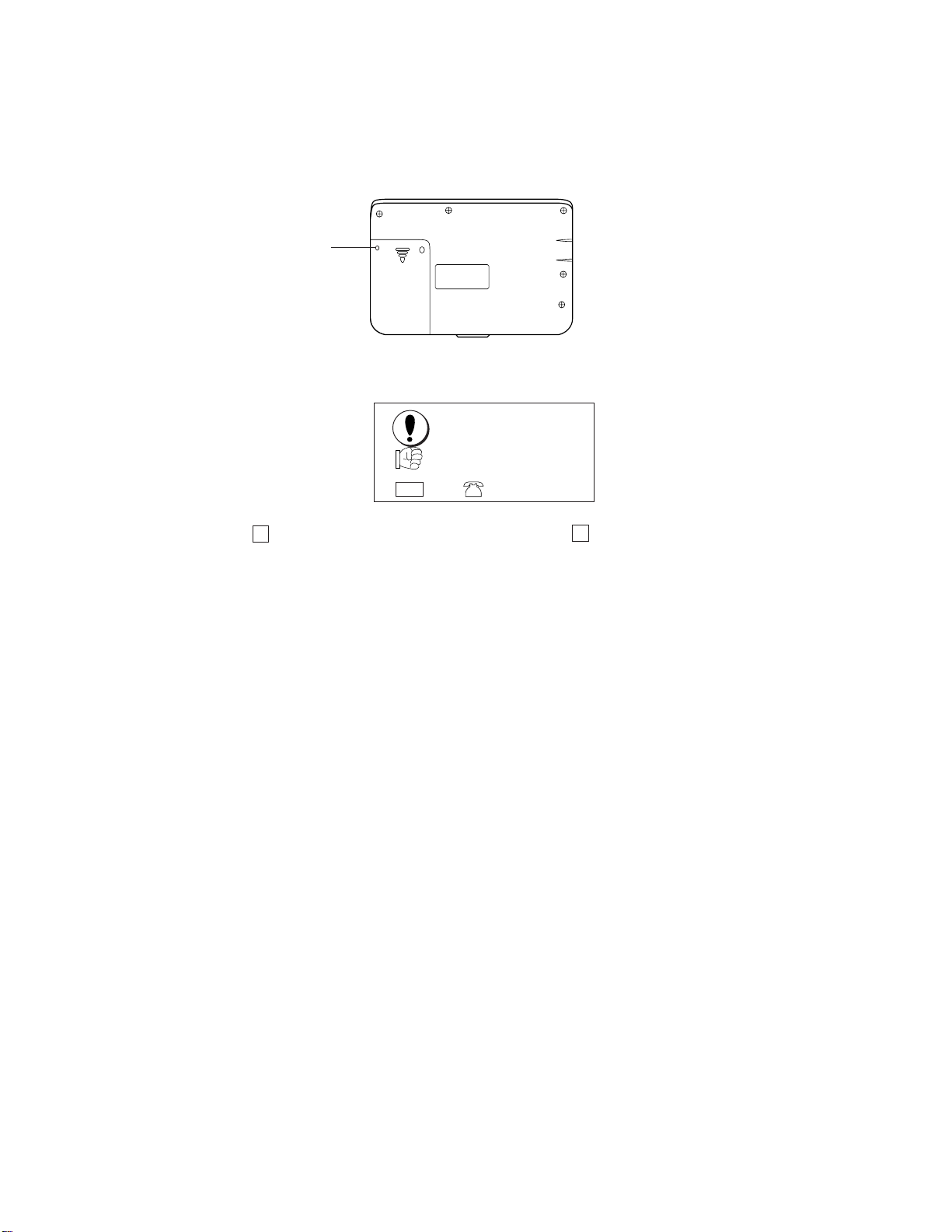
4. RESETTING THE UNIT
The following procedures erase all data stored in the memory of the SF-5300B.
RESET Button
RESET
1. Turn on the unit and press the RESET button with a thin, pointed object.
ALL DATA
CLEAR!
OK? Y/N
CAPS
2. Press Y to reset the memory and delete all data, or N to abort the reset
operation without deleting anything.
Following the reset operation described above, the Home Time display appears and the SF5300B settings are initialized as noted below.
Home Time: 12-hour format
JAN/1/1995
AM/12:00 00
Zone: London(LON)
World Time: New York(NYC)
Sound: Schedule alarm → ON
Reminder alarm → ON
Daily alarm → OFF
Key → ON
Character Input: CAPS
Daily Alarm: 12:00 PM
— 7 —
Page 9
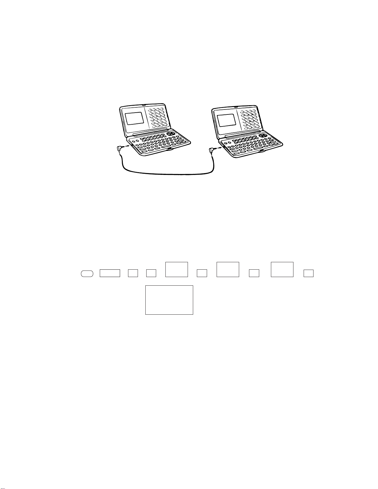
5. SAVING DATA
The SF-5300B can transfer the customer's data (both the open and secret areas) to another SF-5300B.
• Turn off both the transmitting and receiving units and connect them using the SB-60/62 cable.
SB-60/62
1 Setting up the receiving unit:
1. Do the reset operation.
2. Enter the calculator mode. Set the date of receiving unit to February 3rd, 1901.
Operation:
TIME
MENU
ON
Note: The customer may have created a password to protect confidential information from
unauthorized access. To be sure this password is transferred to the receiving unit, be sure
to set the date as described above.
61
M SUN
1901/ 2/ 3
DATE
2
TIME
DATE
TIME
3
DATE
M+
R
— 8 —
Page 10

3. Press , , and twice.
MENU
1
FUNC
1* TO SECRET AREA
2 ALL DELETE
3 LABEL EDIT
4 DATA COMM
CAPS
*If the password isn't
registered in the SF-5300B,
the display shows X instead
of "1."
4. Press to select DATA COMM.
4
1 SEND
2 RECEIVE
3 SET UP PAR.
CAPS
5. Press to select RECEIVE.
2
DATA
CAPS
RECEIVE OK
TO STOP
PRESS (ESC)
— 9 —
Page 11

2 Setting up the transmitting unit:
Set the hardware parameters as follows:
Parity: None Bit length: 7 BPS: 9600
1. Press , , and .
2. Press twice.
ON
FUNC
MENU
1
1* TO SECRET AREA
2 ALL DELETE
3 LABEL EDIT
4 DATA COMM
CAPS
3. Press to select DATA COMM.
4
1 SEND
2 RECEIVE
3 SET UP PAR.
CAPS
4. Press to select SET UP.
3
*If the password isn't
registered in the SF-5300B,
the display shows X instead
of "1."
✻✻ SET UP PAR. ✻✻✻
PARITY E O N
BIT LENGTH 7 8
BPS 4800 9600
CAPS
5. Use , , , or to select "N," "7," and "9600" and press .
SET
1 SEND
2 RECEIVE
3 SET UP
CAPS
— 10 —
Page 12

6. Press to select SEND.
1
1 ONE ITEM
2 MODE DATA
3 ALL DATA
- SEND -
CAPS
7. Press to select ALL DATA.
3
SEND ALL DATA?
SET/ESC
CAPS
8. Press to start data transmission or to abort the operation without sending
SET
ESC
anything.
SENDING
DATA
TO STOP
PRESS (ESC)
CAPS
• If an error occurs during data transmission, the message “TRANSMIT ERROR!” appears on
the display. Press to clear the error message.
ESC
9. After data transmission is complete, the display returns to the initial screen of the telephone
mode.
— 11 —
Page 13

6. LSI PIN FUNCTIONS
6-1. CPU: LSI1
No.1
Pin No. Name I/O Description
1 ~ 5 C0 ~ 4 Out Common signal for display
6 GND In GND 0 V
7,8 BZ1,2 Out Buzzer terminal
9 VDD In Power supply terminal (+5.3 V)
10 CSRA1 Out Chip enable signal for LSI2
11 CSRA2 Out Chip enable signal for LSI3
12 CSROM Out Chip enable signal (Not used)
13 WEB Out Write enable signal for LSI2 and LSI3
14,15 RA15,16 Out Address bus (Not used)
16 ~ 30 A0 ~ 14 Out Address bus
31 ~ 38 IO0 ~ 7 I/O Data bus
39 ~ 54 KY0 ~ 15 I/O Key signal
55 SW In Battery switch Power on: 0 V off: 6 V
56 DEBUG - Not used
57 ON Out Data communication enable signal
58 CRCKI In GND 0 V
59 SOUTB Out Transmission data output
60 SIN In Receiving data input
61 VDD In Power supply terminal (+5.3 V)
62 TEST - Not used
63 VTM - Not used
— 12 —
Page 14
Pin No. Name I/O Description
64,65 OSC I/O I/O Clock terminal
67,69~71 V1 ~ 4 Voltage for LCD drive
OFF: 0 V ON–V1: 0.64 Minimum ~ 1.29 Maximum V
V2: 1.29 Minimum ~ 2.56 Maximum V
V3: 3.99 Minimum ~ 2.71 Maximum V
V4: 4.64 Minimum ~ 3.99 Maximum V
68 NC - Not used
72 INTO In Low battery detection INTO < 5.2 V => No power on
73 STNT - GND 0 V
74 VLCD In Power supply terminal (+5.3 V)
75 ~ 171
172 ~199
168,200 NC - Not used
6-2. RAM: LSI2 and LSI3 (CXK58257)
S0 ~ 95 Out Segment signal for display
C5 ~ 32 Out Common signal for display
22
OE–
23
A11
24
A9
25
A8
26
A13
27
WE–
28
VCC
1
A14
2
A12
3
A7
4
A6
5
A5
6
A4
7
A3
Pin No. Name I/O Description
1~10,21,23~26 A0 ~ 14 In Address bus
11~13,15~19 IO1 ~ IO8 I/O Data bus
14 GND In GND 0 V
20 CE In Chip select signal from LSI1
22 OE In 0 V
27 WE In Write enable signal from LSI1
28 VCC In Power supply terminal (+ 5.3 V)
(LSI 2)
CXK58257ATM
A10
CE–
IO8
IO7
IO6
IO5
IO4
GND
IO3
IO2
IO1
A0
A1
A2
21
20
19
18
17
16
15
14
13
12
11
10
9
8
— 13 —
Page 15

6-3. VOLTAGE REGULATOR: REG1 (S-81253)
Output Voltage (VDD): 5.3 V ± 5%
VCC
GND
2
R
A
+
V
–
REF
R
B
1
6-4. VOLTAGE DETECTOR: DET1 (RH5VL46CA)
VCC
2
OUT
1
3
VDD
R
I
1
GND2VCC
3
VDD
3
2
1
GND
VCC
OUT
3
GND
Input Voltage (VCC) Output Voltage (OUT)
VCC > 5.2 V 5.2 V
VCC < 5.2 V 0 V
— 14 —
Page 16

7. TROUBLESHOOTING
No power on
START
Is the display contrast adjustment OK?
Are the power of batteries strong enough?
N
Adjust the display contrast.
Y
N
Replace the batteries.
Y
Does the display appear by pressing
the reset button?
N
Does the unit sound with each key entry?
N
Do the batteries make positive contact
with the battery springs?
Y
Y
Is Pin 3 of REG1 5.3 V?
N
Are the capacitors C8, C9, C10, C11,
C12, and C13 OK?
Y
Y
Check another function.
Y
Refer to "No/Erratic Display."
N
N
Adjust the contact and clean the
battery springs.
Replace C8, C9, C10, C11, C12, or
C13.
Replace REG1.
1
— 15 —
Page 17

1
Is Pin 1 of DET1 5.2 V?
Y
Is Pin 11 of LSI1 sending the signal?
Y
Is Pin 13 of LSI1 sending the signal?
Y
Is the soldering of LSI2 or LSI3 poor?
N
Replace LSI1, LSI2, or LSI3.
N
Replace DET1.
N
Replace LSI1.
N
Replace LSI1.
Y
Resolder.
No key input
START
Does the rubber key contact make positive
contact with the PCB assembly?
Y
Is the soldering of LSI1 poor?
N
Replace LSI1.
N
Replace the rubber key contact.
Y
Resolder.
— 16 —
Page 18

No/Erratic display
START
Are the power of batteries strong enough?
Y
Is input Pin 2 of REG1 6 V?
Y
Is output Pin 3 of REG1 5.3 V?
Y
Are the voltages of V1, V2, V3, and V4
strong enough?
V1: 1.3 V
V2: 2.5 V
V3: 2.7 V
V4: 3.9 V
Note:
Contrast: Maximum
N
Replace the batteries.
N
N
N
Adjust the contact and clean
the battery springs.
Replace REG1.
Replace C1, C2, C3, or C4.
Is the soldering of LSI1 poor?
Replace LSI1.
High current consumption
START
Is there any short circuit on the PCB
assembly ?
Are the capacitors C8, C9, C11, C12,
and C13 OK?
Y
Y
Resolder.
N
Y
Repair shorts.
N
Y
Resolder or replace LSIs and ICs.
N
Replace the capacitor(s).
— 17 —
Page 19

Blind Label
Battery Switch
Check Pads
8. DIAGNOSTICS
Notes: 1. Be sure to transfer data to another SF-5300B unit before entering
the diagnostic mode, because the data will be changed by entering
the diagnostic mode.
2. The shorting pads shown in the following illustration are covered by a
blind label.
3. To exit the diagnostic mode, press the reset button.
To enter the diagnostic mode:
1. Slide the battery switch to the up position.
2. Press while shorting the shorting pads.
3. Press .
ON
SELF TEST PROG.
PRESS SEARCH
QUIT BY OFF
CASIO APR 1994
SEARCH
TEST 2 MEMORY
MENU 3 KEY
4 BUZZER
1 DISP 5 I/F
5 I/F: Not used
— 18 —
Page 20

Display Check
Operation Display Note
Press 1 on the TEST MENU.
1
2
DISP 4 RVS.
1 WHITE 5 FRAME
2 BLACK 6 DOT4
3 CHECK. 7 TIME
Display check
To return to the
TEST MENU,
ESC
press .
No display
All dots displayed
4
5
3
ACC CAPS SHIFT
,
Checker displayed
SEARCH
Reverse checker
display
Frame display
— 19 —
Page 21
Operation Display Note
6
7
ESC
Memory Check
TIME DISPLAY
00:00:XX
TEST 2 MEMORY
MENU 3 KEY
4 BUZZER
1 DISP 5 EXT
Shows dots at
corners.
Check to see if
timer is working.
The functions of the numbered items on the display include:
1. Writes the test pattern in the ROM to the RAM area. (Test pattern: Incremental order 00,
01, and so on)
2. Compares the test pattern with the write data (WRITE1) of the RAM and displays the
results.
3. Writes the test pattern in the ROM to the RAM area. (Test pattern: Decremental order
FF, FE, and so on)
4. Compares the test pattern with the write data (WRITE2) of the RAM and displays the
results.
Operation Display Note
2
1
( or 3 )
MEMORY 3 WR2
4 READ2
1 WR1 5 DUMP
2 READ1 6 CHKSUM
WRITE1
( or WRITE2 )
RAM check
To return to the
TEST MENU,
press .
ESC
5: Not used
6: Not used
— 20 —
Page 22

Operation Display Note
(After a few seconds)
2
( or 4 )
MEMORY 3 WR2
4 READ2
1 WR1 5 DUMP
2 READ1 6 CHKSUM
EXECUTING!!
COMPLETE!!
64KB
DATA ERROR!!
ADDRESS CORR RAM
XXXX XX XX
RAM error
If the displayed address
is within 0000-7FFF,
check LSI3.
If the displayed address
is within 8000-FFFF,
check LSI2.
ESC
MEMORY 3 WR2
4 READ2
1 WR1 5 DUMP
2 READ1 6 CHKSUM
Key Check
Each key has its own key code. The key codes are assigned incrementally from left to right on the key
board. (Refer to the keyboard in the schematic diagrams.)
In the auto mode, the key input sequence is limited so that the keys must be pressed in the order of the
key code as mentioned above. If a key is pressed in the wrong order, the SF-5300B beeps.
Operation Display Note
Key check
To return to the
TEST MENU,
press .
ESC
Press 3 on the TEST MENU.
2
KEY 1 RANDOM
2 AUTO
No display
— 21 —
Page 23

Operation Display Note
MC MR M– M+
AC , ... % 7 , ... ÷
4 , ... x 1 , ... –
0 , ... + ON OFF
EXPENSE , ... DISP CHNG
REMINDER , ... DEL
← ↑ ↓ → ESC , ... ( )
FUNCTION , ... SHIFT , ...
SHIFT CAPS , ... SET
SEARCH
Buzzer Check
Operation Display Note
Press 4 on the TEST MENU.
00 01 02 03 04 ...............
............... 56 57
TEST 2 MEMORY
MENU 3 KEY
4 BUZZER
1 DISP 5 EXT
BUZZER 1 BEEP
2 ALARM1
3 ALARM2
Check that the key
number appears on
the display.
To return to the TEST
MENU, enter
SEARCH .
Buzzer check
To return to the
TEST MENU,
press .
ESC
1
( or 2 , 3 )
ESC
EXECUTING!!
BUZZER 1 BEEP
2 ALARM1
3 ALARM2
TEST 2 MEMORY
MENU 3 KEY
4 BUZZER
1 DISP 5 EXT
Check the sound.
To return to the
BUZZER menu,
press any key.
— 22 —
Page 24

17
38
18
19
22
21
23
24
25
39
39
38
16
14
13
39
15
12
11
20
9
38
1
2
3
4
6
31
41
8
5
32
26
6-1
33
34
30
27
42
35
41
6-2
28
40
37
9. ASSEMBLY VIEW
10
36
29
39
41
7
— 23 —
Page 25

10. PARTS LIST
FOB Japan
N Item Code No. Parts Name Specification Q M N.R.Yen R
Unit Price
DISPLAY PCB ASS'Y
N 1 6412 2750 Display PCB ass'y DB22XX3F01M
(Consists of the following:)
C1~4,7,8,12,13,14 2845 1540 Chip capacitor MCH212F104ZK
C5,6 2845 1652 Chip capacitor MCH215A180JK
N LSI1 6411 6351 COF sub ass'y C312133*3
N LSI2 2011 8267 LSI CXK58257ATM-10/12L
N LSI3 2011 8274 LSI CXK58257AYM-10/12L
N LSI4 2011 9149 LSI µPD23C1001EAGZ-M04
X1 7110 0642 Crystal oscillator DT-26S
N R3 2797 3752 Chip resistor ERJ-6GEYJ000
N R4 2797 3752 Chip resistor ERJ-6GEYJ000
R11 2791 0777 Chip resistor ERJ-6GEYJ104
N R12 2797 3857 Chip resistor ERJ-6GEAK206
KEYBOARD PCB ASS'Y
N 6 6412 2730 Keyboard PCB ass'y DB22XX3100U
(Consists of the following:)
C9,11 2803 6806 Electrolytic capacitor 10MS510M-MW
C10 2845 1540 Chip capacitor MCH212F104ZK
D1 2390 2128 Chip diode MA740-(TX)
D2 2390 0364 Schottky diode MA713-(TX)
DET1 2105 3864 CMOS IC RH5VL46CA-T1
REG1 2105 3290 CMOS IC S-81253SGUP-DIJ-T1
J1 3501 6538 Jack HSJ1169-012010
N R5 2797 3759 Chip resistor ERJ-6GEYJ182
R6 2797 0637 Chip resistor ERJ-6GEYJ473
R7 2797 1309 Chip resistor ERJ-6GEYJ102
R8,9 2797 1078 Chip resistor ERJ-6GEYJ101
N R20 2797 3752 Chip resistor ERJ-6GEYJ000
Q1 2259 0959 Chip digital transistor DTC114YKT-146
6-1 6409 6300 Spring Battry (+) EF01DB20102
6-2 6409 6310 Spring Battry (-) EF02DB10100
COMPONENT
N 2 6412 3110 Protection tape HGJ00008406
3 6412 3140 Heat seal FX21P250016
N 4 6412 3120 Protection tape HGJ00008201
N 5 6412 2920 Insulation plate EL4J0002102
7 6511 7160 Cap LC120000102
8 6412 2890 Key contact rubber LADB2210000
9 6512 0730 Hinge stopper EF15DB06102
10 6412 2880 Push button FB3DB221002
11 6412 3020 Upper case (KB) FAADB221009
N 12 6412 3050 Hinge (A) FC0DB281006
13 6512 1210 Pin FC002870000
14 6512 1220 Pin (L) FC002870018
N 15 6412 2910 Hinge (B) FC0DB222002
N 16 6412 2990 Hinge blind tape HGJ00008309
N 17 6412 2940 Display plate EL5J0005103
N 17 6412 2950 Display plate (for B.O.S.S.) EL5J0005201
18 6412 3040 Upper case (DIS) FAADB222005
19 6412 3130 Heat seal FX200P40064
20 3335 5264 LCD CD792-TS
Notes: N – New parts R – A : Essential
M – Minimum order/supply quantity B : Stock recommended
R – Rank C : Others
Q – Quantity used per unit X : No stock recommended
1 2,730 B
1
20 4 C
8
20 3 C
1
1 970 B
1
1 580 B
1
1 580 B
1
1 370 B
1
557B
1
20 2 C
1
20 2 C
1
20 5 C
1
20 2 C
1
1 790 B
1
20 13 C
2
20 4 C
1
10 50 C
1
10 33 C
1
10 45 C
1
560C
1
556C
1
20 2 C
1
20 2 C
1
20 3 C
1
20 3 C
2
20 2 C
1
20 12 C
1
20 16 X
2
20 16 X
2
20 19 B
1
553A
1
20 26 B
1
10 29 X
1
20 17 B
1
1 260 C
1
20 27 X
2
20 13 C
1
1 130 X
1
20 26 X
1
20 9 X
2
20 16 X
2
20 22 X
1
20 22 B
1
1 120 B
1
1 120 B
1
1 110 X
1
1 100 A
1
1 790 A
1
— 25 —
Page 26

FOB Japan
N Item Code No. Parts Name Specification Q M N.R.Yen R
Unit Price
21 6411 8460 Cushion FH100027205
22 6412 2900 Key contact rubber LADB2220005
23 6412 3160 Heat seal FX201P50209
N 24 6412 3150 PCB DADB22XX309
N 25 6412 2840 Lower case (DIS) FABDB222001
N 25 6412 2850 Lower case (DIS) (for B.O.S.S.) FABDB222010
26 6409 6120 Battery holder ECDB1011108
27 6409 6210 Battery change label HGC00001102
28 6412 3060 Battery cover FADDB221001
29 6409 6230 Battery cover label HGC00001200
N 30 6412 2980 Blind tape HGJ00008104
N 31 6412 3070 Lower case (KB) FABDB221005
N 31 6412 3080 Lower case (KB) (for B.O.S.S.) FABDB221013
32 6511 8400 Key rubber for reset LADB0220105
33 6512 1080 Nut MD100000602
34 6510 4440 Blind tape HGFC0001206
35 6408 5920 Switch ass'y DB2AXX4A00M*1
36 6510 4500 Buzzer tape HGFC0000501
37 3122 2380 Buzzer EFB-S55C41A8
38 6406 1610 Screw MAB20091300
39 6512 1000 Screw MABA0004207
40 6510 4350 Decoration screw MAA80006302
41 6512 0980 Screw MAB20086306
42 6510 4310 Decoration screw MAA80006311
565C
2
1 103 C
1
590A
1
563X
1
1 110 X
1
1 110 X
1
20 26 X
2
20 7 X
1
20 29 X
1
20 16 X
1
20 7 X
1
582X
1
582X
1
20 10 B
1
20 13 X
3
20 6 X
3
20 30 C
1
20 17 X
1
10 36 X
1
20 5 B
5
20 3 B
10
20 2 B
1
20 2 B
8
20 3 B
2
Notes: N – New parts R – A : Essential
M – Minimum order/supply quantity B : Stock recommended
R – Rank C : Others
Q – Quantity used per unit X : No stock recommended
— 26 —
Page 27

MA1100741A
 Loading...