

Page 1
SF-4300A(LX-571AT)
INDEX
SF-4600(LX-571ET/FT)
JAN. 1993
(without price)
R
Page 2

CONTENTS
1. SCHEMATIC DIAGRAM.................................................................................................... 1
2. SPECIFICATIONS ............................................................................................................. 3
3. TO REPLACE THE BATTERIES....................................................................................... 4
4. DATA TRANSFER............................................................................................................. 5
5. BLOCK DIAGRAM ............................................................................................................ 9
6. LSI, IC (Pin Function) ..................................................................................................... 10
7. To FIX TAB ASS'Y ........................................................................................................... 13
8. TROUBLE SHOOTING.................................................................................................... 14
9. HARD CHECK ................................................................................................................. 17
10. DATA TRANSFER CHECK ............................................................................................. 22
11. PCB VIEW........................................................................................................................ 26
12. ASSEMBLY VIEW ........................................................................................................... 27
13. PARTS LIST .................................................................................................................... 29
Page 3
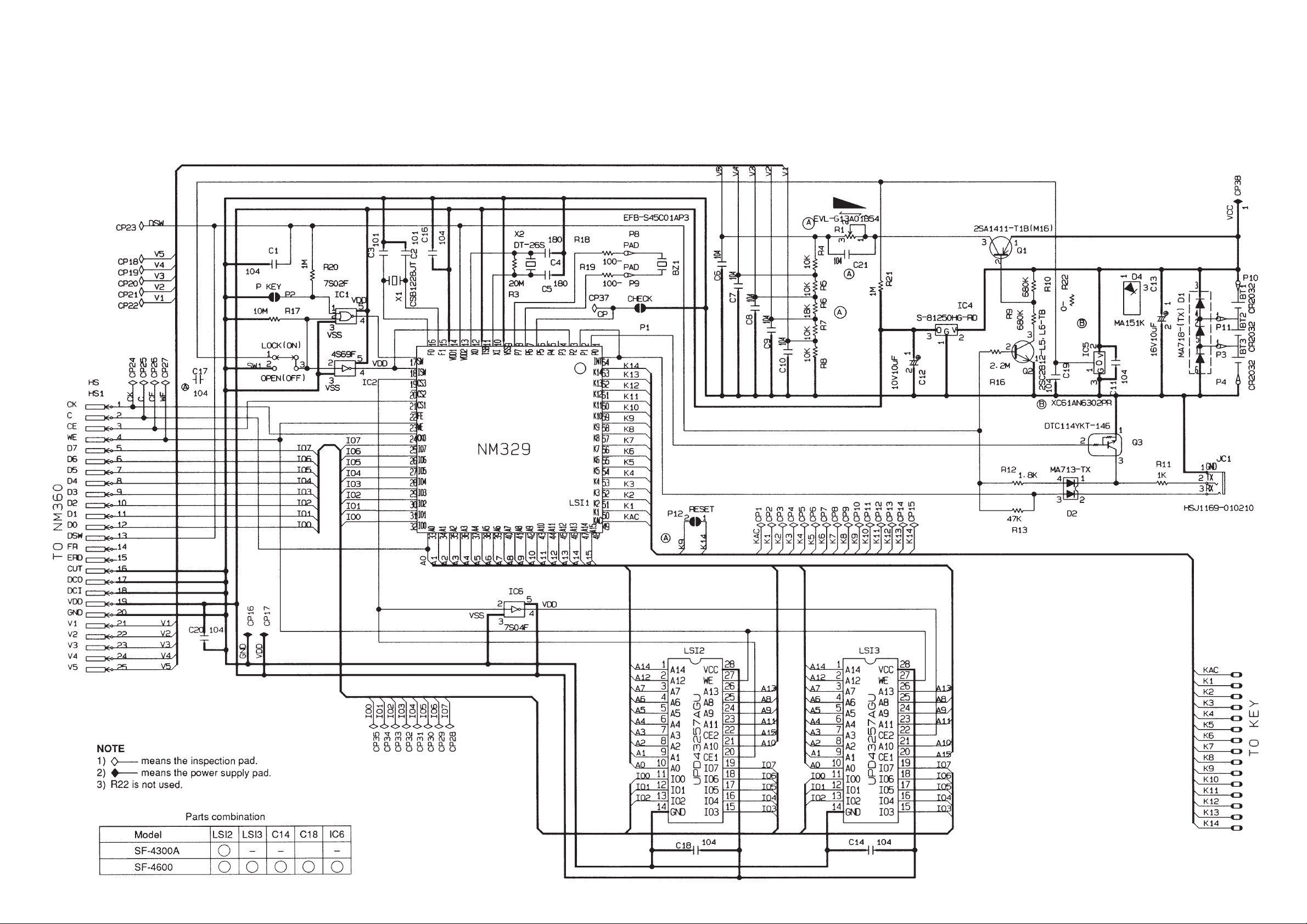
1. SCHEMATIC DIAGRAM
1-1. MAIN PCB
— 1 —
Page 4
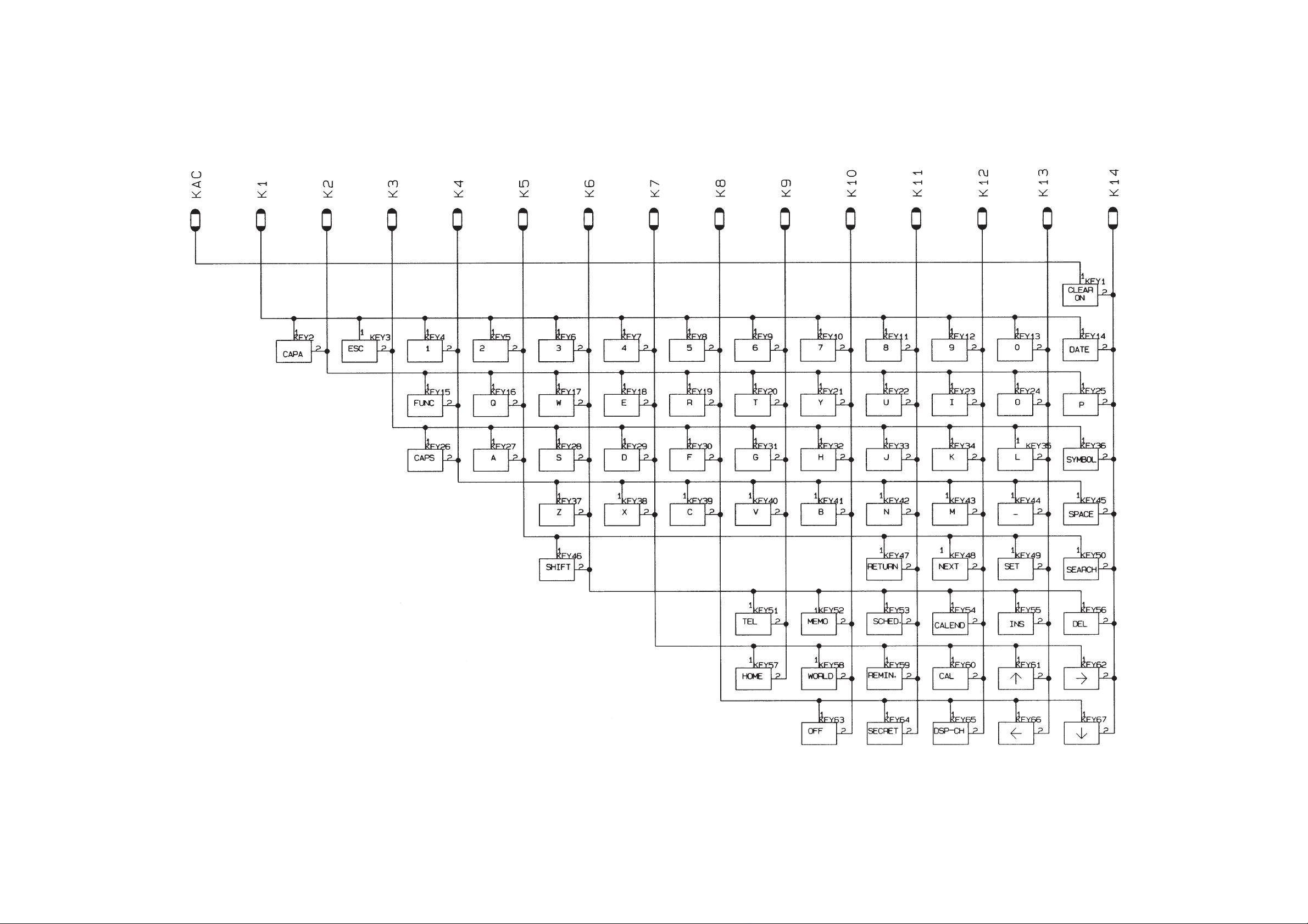
1-2. KEY MATRIX
— 2 —
Page 5
2. SPECIFICATIONS
Data storage:
Storage and recall of telephone, memo, schedule, reminder data; calendar display; mark
protection; secret area; editing; memory status display
Clock:
World time; reminder alarm; schedule alarm; daily alarm; accuracy under normal temperatures: ±3 seconds average
Calculation:
10-digit arithmetic calculations; arithmetic constants (+, –, ×, ÷); independent memory;
percentages; square roots; 20-digit approximations; date calculations; other mixed calculations
General:
Display element: 16-column × 4-line LCD
Memory capacity: 32 KB / SF-4300A, 64 KB / SF-4600
Main component: LSI
Power supply: 3 lithium batteries (CR2032)
Power consumption: 0.05W
Battery life: Approximately 200 hours continuous operation in Telephone Directory
approximately; 150 hours repeating one minute of input and 10 minutes
of display in Telephone Directory; approximately 12 months for memory
back up
Test condition: 20°C
Auto power off: Approximately 6 minutes after last key operation
Operating temperature: 0°C ~ 40°C (32°F ~ 104°F)
Dimensions:
Unfolded: 12.4H
Folded: 8.9H
Weight: 110g (3.9 oz)
x 141W x 80.5Dmm (1/2"H x 5-5/8"W x 3-1/8"D)
x 141W x 157Dmm (3/8"H x 5-5/8"W x 6-1/4"D)
Current consumption:
Power switch MIN. [µA] MAX [µA]
OFF 9.51
ON 529 606
ON 1,287 1,398
(Operating)
— 3 —
Page 6
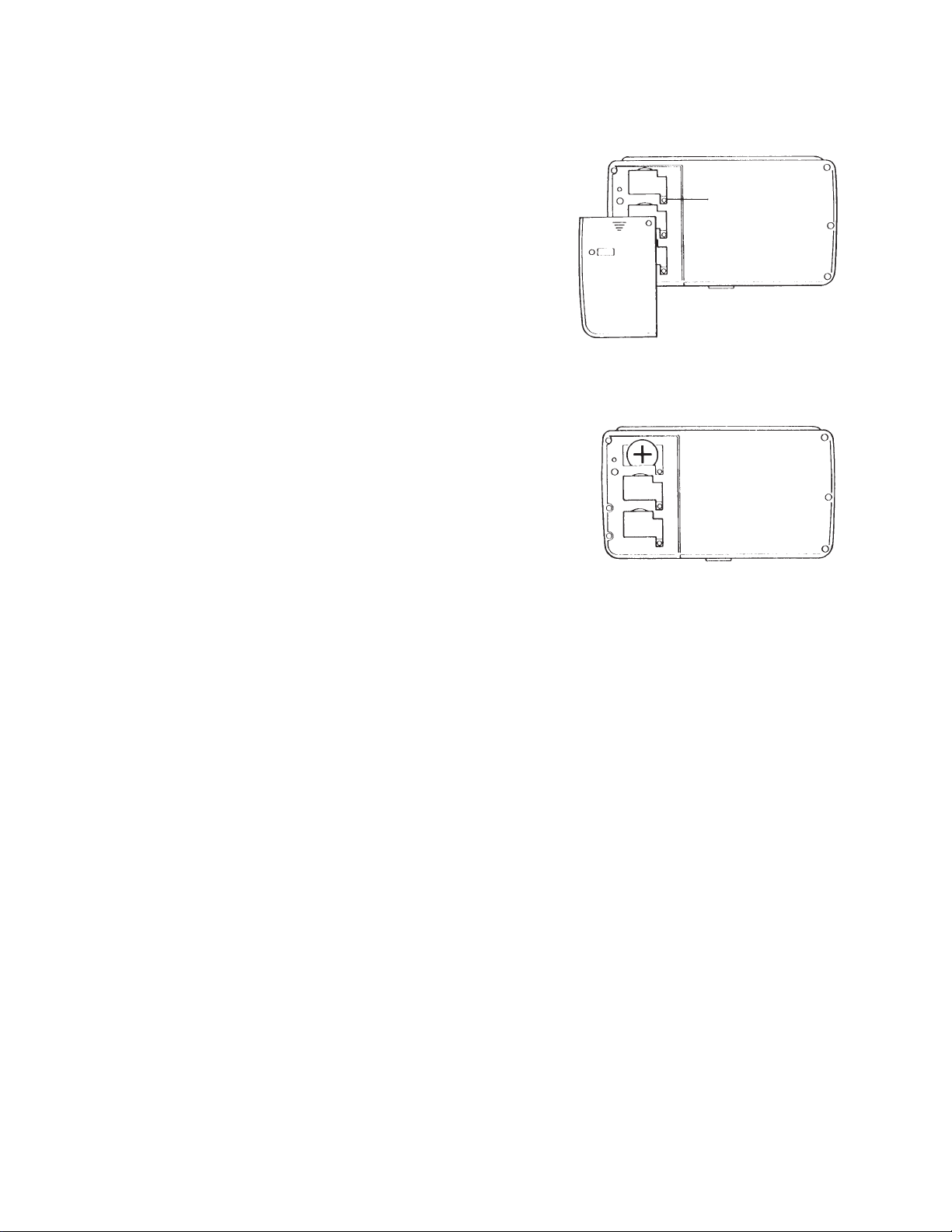
3. TO REPLACE THE BATTERIES
1) Loosen the screw on the back of the SF-4300A /
SF-4600 that holds the battery compartment
cover in place, and remove the cover.
2) Loosen the screw that secures one of the three
battery holders in place and remove the battery
holder.
Caution
Be sure to remove only one battery at a time.
Otherwise, you will lose all data stored in memory.
3) Replace the old battery with a new one, making
sure that the positive (+) side of the new battery
is facing up (so you can see it).
Screw
4) Replace the battery holder and secure it by tightening its screw.
• Be sure careful that you do not over tighten the screw.
5) Repeat steps 2) through 4) for the other two batteries.
• Be sure to replace all three batteries. Never mix old batteries with new ones, and be sure
to use CR2032 lithium batteries only.
6) After you replace all three batteries, replace the battery compartment cover and secure it
by tightening its screw.
• Be careful that you do not over tighten the screw.
— 4 —
Page 7
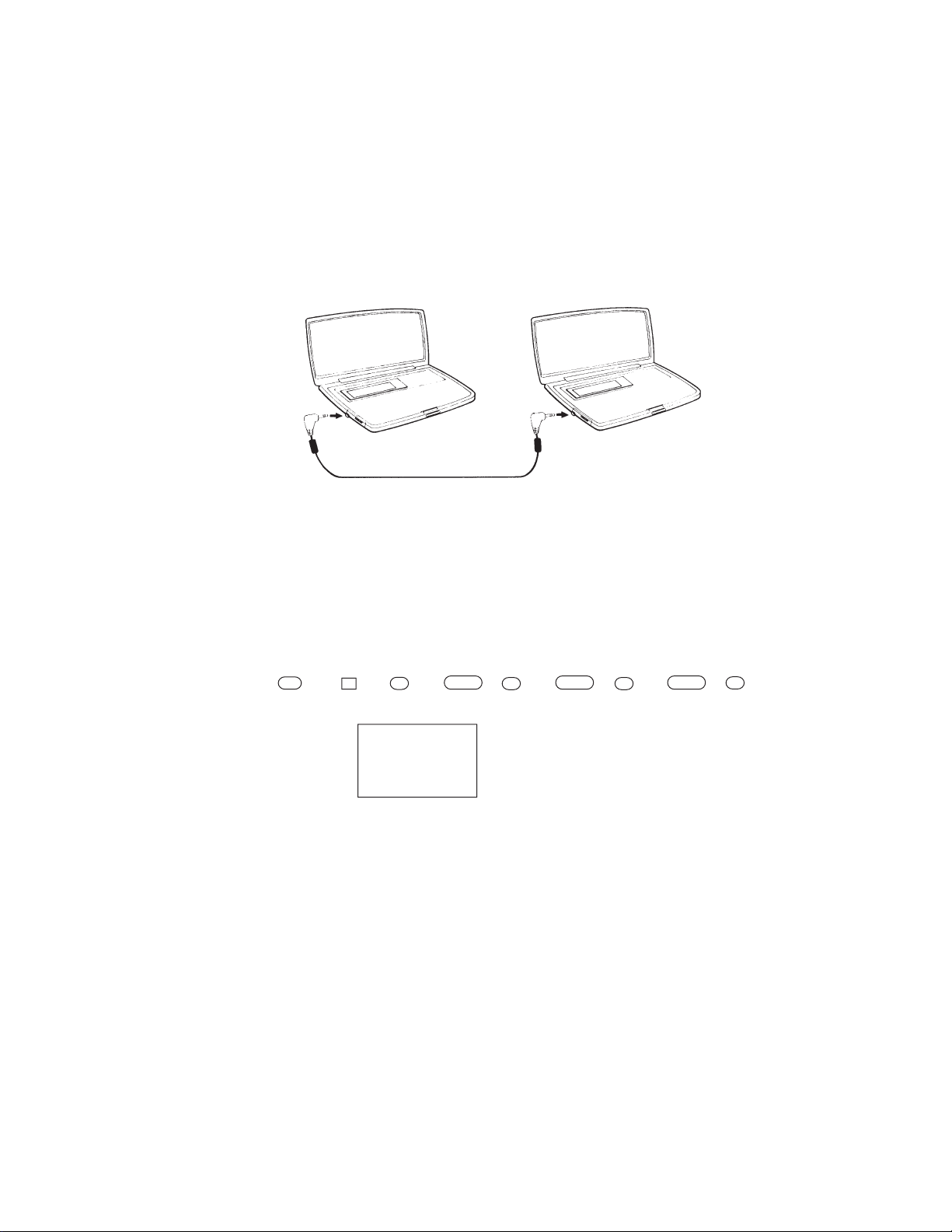
4. DATA TRANSFER
SF-4300A / SF-4600 can transfer customers data to other SF-4300A / SF-4600 with memory
protection only when replacing the LCD or the outer case. How to transfer the data.
* Before connecting the cable (SB-60/62), be sure to reset the slave machine to clear all
data.
1) Turn off the power switch and connect the two units using the cable (SB-60/62) as shown
in the drawing.
SB-60/62 accessory cable
2) Turn on the power switch of each machine.
3) The slave machine must be set the date of Feb. 3rd, 1901 into the memory under the
calculator mode.
Operation:
ON CAL TIME TIME TIME M+
123
M SUN
1901/ 2/ 3
DATE DATE DATE R
If you don't set the date, the "PASSWORD" isn't transferred to the slave machine.
— 5 —
Page 8
Setting up for Data Communications
The following procedures describe what you should do to set up for data communications
between two SF Units or between an SF Unit and a personal computer. In addition to
hardware connections, it details how to set up the communications parameters and how to
set up the SF-4300A / SF-4600 to receive data. By following these instructions carefully,
you can be ensured of successful communications every time.
To connect two SF Units
1. Check to make sure that the power of the two SF Units is switched off.
2. Remove the covers from the connectors on the two SF Units.
3. Connect the two SF Units using the optional SB-60/62 cable. You can also connect
them using an SB-60/62 cable.
Important
Be sure to replace the connector covers on the SF Units when you are not performing data
communications.
4) Check the hardware parameters.
1 While an initial screen is displayed, press FUNC twice to display the second function
menu.
FUNC FUNC
2 ALL DELETE
3 LABEL EDIT
4 DATA COMM
CAPS
• You can perform the above operation while the initial screen of the Telephone
Directory, Memo Mode, Schedule Keeper, Calendar, Reminder is displayed.
2 Press 4 to select DATA COMM.
4
1 SEND
2 RECEIVE
3 SET UP
4 FDD
CAPS
3 Press 3 to select SET UP.
3
SET UP
PARITY E O N
BIT LENGTH 7 8
BPS 2400 4800
CAPS
— 6 —
Page 9
4 If the units have another condition, reset as above.
• To change the parameters
1. Use the ∆ and — cursor keys to change the selected parameter on the display.
2. Use the and cursor keys to change the high-lighted setting of the currently
selected parameter.
SET
3. Press SET to store them in memory.
5) Set up the slave machine
1 While an initial screen is displayed, press FUNC twice to display the second function
menu.
FUNC FUNC
• You can perform the above operation while the initial screen of the Telephone
Directory, Memo Mode, Schedule Keeper, Calendar, Reminder is displayed.
2 Press 4 to select DATA COMM.
4
∇
∆
2 ALL DELETE
3 LABEL EDIT
4 DATA COMM
CAPS
1 SEND
2 RECEIVE
3 SET UP
4 FDD
CAPS
3 Press 2 to select RECEIVE.
2
RECEIVE OK
DATA
CAPS
TO STOP
PRESS (ESC)
6) Set up the customer’s machine.
1 While an initial screen is displayed, press FUNC twice to display the second function
menu.
FUNC FUNC
2 ALL DELETE
3 LABEL EDIT
4 DATA COMM
CAPS
• You can perform the above operation while the initial screen of the Telephone
Directory, Memo Mode, Schedule Keeper, Calendar, Reminder is displayed.
— 7 —
Page 10
2 Press 4 to select DATA COMM.
4
1 SEND
2 RECEIVE
3 SET UP
4 FDD
CAPS
3 Press 1 to select SEND.
1
1 ONE ITEM
2 MODE DATA
3 ALL DATA
CAPS
4 Press 3 to select ALL DATA.
3
SEND ALL DATA?
- SEND -
SET/ESC
CAPS
5 Press SET to start the send operation or ESC to abort the operation without sending
anything.
SET / ESC
SENDING
DATA
TO STOP
PRESS (ESC)
CAPS
• Data is send in the sequence: Telephone Directory, Memo Mode, Reminder Mode,
Schedule Keeper, Calendar.
• To abort the send operation at any time, press ESC.
• If an error occurs during the send operation, the message “SEND ERROR!” appears
on the display. Press ESC to clear the error message.
6 After the send operation is complete, the display returns to the initial screen of the mode
you were in when you started this procedure.
— 8 —
Page 11

5. BLOCK DIAGRAM
TAB Ass'y
LCD
SF-4300A LD-B8272AY
SF-4600 CD408-TS
L571-1 Ass'y
Contrast
V1~V5
VDD1
NM360
LCD diriver
CPU
µPD3056G-007
SW, ISW
ON OFF
Data Bus
P0P1
CONTRASTV1 V2 V3 V4 V5
Max.(V) 1.5 3.0 5.5 7.0 8.5
Min.(V) 1.0 2.0 4.0 5.0 6.0
Address
Bus
RAM
µPD43257AGU
-10/12LL
RAM
µPD43257AGU
-10/12LL
KAC,
K1~K14
KEYBOARD
LCD
Voltages
switching
circuit
VCC
VDD2
VDD
S-81250
HG-RD
XC61AN
6302PR
Power Supply
Battery
(CR-2032 X 3)
— 9 —
Tx
Jack
Rx
GND
Page 12

6. LSI, IC (Pin function)
6-1. CPU: µPD 3056G-007 (LSI 1)
48 47 46 45 44 43 42 41 40 39 38 37 36 35 34 33
49
50
51
52
53
54
55
56
57
58
59
60
61
62
63
64
µPD 3056G-007
1 2 3 4 5 6 7 8 9 10 11 12 13 14 15 16
32
31
30
29
28
27
26
25
24
23
22
21
20
19
18
17
Pin No. Signal I/O Function
1 ~ 8 P0 ~ 7 I/O PORT P0: I/F output P1: I/F input
9 VSS I GND (0V)P6, P7: For buzzer
10 XI I Clock input
11 TSB Test Terminal
12 X0 O Clock output
13 VDD2 O
Internal power supply terminal
Power OFF: 0V ON: 5V
14 VDD1 I Power supply terminal (+5V)
15 FI I Internal clock terminal
16 FO O Internal clock terminal
17 SW I Main switch signa Power ON: 0V OFF: 5V
18 ISW I Sub switch signal Power ON: 0V OFF: 5V
19 ~ 21 CS1 ~ 3 O Enable signal for RAM
22 FE O Enable signal for ROM
23 WE O Write enable signal for RAM
24 CKO O Clock signal for LCD driver (NM360)
25 ~ 32 IO0 ~ 7 I/O Data bus
33 ~ 48 A0 ~ 15 O Address bus
49 ~ 63 KAC ~ K14 Key signal from keyboard
64 INT I Interrupt terminal
— 10 —
Page 13

6-2. RAM: µPD43256G-101215LL (LSI 2)
6-4. LCD driver: NM 360
µPD3056G-007 (WE)
µPD3056G-007 (CS3)
A0 ~ A14 : Address input signal
IO0 ~ IO7: Data signal (Input/Output)
WE : Write enable signal
CS : Chip select signal
OE : Output enable signal
— 11 —
Page 14

6-5. VOLTAGE REGULATOR: S-81250HG-RD (IC3, IC4)
Output Voltage (Vout) : 5V ± 5%
[4.75V (MIN) ~ 5.25V (MAX)]
6-6. VOLTAGE DETECTOR: RH5VA60AA-T1 (IC5)
Detection Voltage(–VDET) : 6V ± 2.5%
[5.85V (MIN) ~ 6.15V (MAX)]
1
GND2Vin3Vout
2
1
Vout
Vin
3
GND
Input voltage Output voltage
>6V 5V
<6V 0V
— 12 —
Page 15

7. TO FIX TAB ASS'Y
When fixing a TAB ass'y part to the main PCB, it is necessary to paint "Neji lock" after soldering the
cable to the place of soldering part for the against of a shock.
1) Parts code of "Neji lock"
Code No. Name Specification Unit Price (FOB:JAPAN)
0001 9829 Neji lock 1402B YEN1,590.-
2) Location of the painting part
TAB Ass'y
Painting place
— 13 —
Page 16

8. TROUBLE SHOOTING
<No power on>
Is contrast adjustment OK?
Is power of batteries enough?
N
Adjust contrast
Y
N
Replace batteries
Y
Does display appear by pressing
Reset button?
N
Does it sound by key enter?
N
Do batteries make positive contact
with the battery springs?
Y
Does CSB1228JT (X1) output clock
pulses?
Y
Y
Is 1-pin of XC61AN6302PR (IC5)
5 [V]?
Y
Check other function
Y
Refer to <No/Erratic display>
N
N
Adjust contact and clean battery spring
Replace X1
N
Are capacitor C11, C19, C12, C13 OK?
Y
Replace IC5
Is 2-pin of TC7SO2F (IC 1) 5[V]?
Y
1
— 14 —
N
Replace C11, C19, C12, C13
N
Adjust/Replace slide switch
Page 17

1
Is 17-Pin of µPD3056G -007(LSI 1)
0[V]?
Y
Is 18-Pin of µPD3056G-007 (LSI 1)
0[V]?
Y
Y
Is 3-Pin of S-81250HG-RD (IC4) 5[V]?
N
Are capacitor C12, C13 OK?
Y
Replace IC4
N
Replace IC1
N
Replace TC4S69F (IC2)
N
Replace C12, C13
Refer to <No/Erratic display>
<No key input>
Does key make positive contact with
L571-1 Ass’y
Y
Replace µPD 3056G-007 (LSI1)
N
Clean/Adjust contact
— 15 —
Page 18

<No/Erratic display>
Is input 2-Pin of S-81250 HG-RD
(IC3) 9[V]?
Y
Is output 3-Pin of S-81250 HG-RD
(IC3) 5[V]?
Y
*
Are voltage of several capacitors enough?
V1: 1.5 [V]
V2: 3.0 [V]
V3: 5.5 [V]
V4: 7.0 [V]
V5: 8.5 [V]
Y
Does TAB ASS’Y make positive
contact with L571-1 ASS’Y?
*CONTRAST: MAX
N
Check Q1, Q2
N
Replace IC3
N
N
Check solder part of R4~R8 or
Replace C6, C7, C8, C9, C10
Resolder
Replace TAB ASS’Y
Resolder/Replace LSI1
<High current consumption>
Is there any short circuit?
Are the several capacitors OK?
Resolder/Replace LSI, IC
Y
Y
Check PCB
N
Y
Replace capacitors
N
— 16 —
Page 19

9. HARD CHECK
No. OPERATION DISPLAY NOTE
1. Turn the slide (battery) switch
1
off.
2. Push the P-button.
Turn the slide (battery) switch on
2
while short the short pad (T16,
T37).
3ON
41
51
00:00:00
TEST 2 MEMORY
MENU 3 KEY
4 BUZZER
1 DISP 5 EXT
DISP 4 RVS.
1 WHITE 5 FRAME
2 BLACK 6 DOT 4
3 CHECK. 7 TIME
No display
Check if timer is
working.
Display check
62
73
All dots display
Checker display
— 17 —
Page 20

No. OPERATION DISPLAY NOTE
84
Reverse checker display
95
FRAME
10 6
Dots appear at corners.
11 7
12 ON
13 3
14 2
00:00:00
TEST 2 MEMORY
MENU 3 KEY
4 BUZZER
1 DISP 5 EXT
KEY 1 RANDOM
2 AUTO
No display
Check if timer is
working.
Key check
— 18 —
Page 21

No. OPERATION DISPLAY NOTE
15
TEL MEMO SCHEDULE CALENDAR
HOME WORLD OFF ON
▲
FUNCTION Q W ................... NEXT
CAPA CAPS A S...................... SET
SHIFT DATE Z X.................SPACE
▲
▼
ESC .....................DEL
▼
÷
16 SEARCH
17 4
18 2
00 01 02 03 04 ...............
TEST 2 MEMORY
MENU 3 KEY
4 BUZZER
1 DISP 5 EXT
BUZZER
1 BEEP
2 ALARM1
3 ALARM2
EXECUTING
• Check the key no.
appears on the display.
• Check the key sounds.
• To return to the menu
mode, enter SEARCH .
Buzzer check
Check the alarm 1
sound.
19 ESC
20 ON
21 2
BUZZER
1 BEEP
2 ALARM1
3 ALARM2
TEST 2 MEMORY
MENU 3 KEY
4 BUZZER
1 DISP 5 EXT
RAM check
MEMORY 3 WR2
4 READ2
1 WR1 5 DUMP
2 READ1 6 CHKSUM
— 19 —
Page 22

No. OPERATION DISPLAY NOTE
22 1
WRITE1
23 (After few seconds)
1. Remove the main batteries.
24
2. Measure the voltage between T16 (GND) and T17
(VDD).
3. Check the voltage is higher
than 2 [V].
4. Set the main batteries.
25
1. Turn the slide switch off.
2. Push the P-button.
3. Turn the slide switch on .
26 ON
MEMORY 3 WR2
4 READ2
1 WR1 5 DUMP
2 READ1 6 CHKSUM
00:00:00
TEST 2 MEMORY
MENU 3 KEY
4 BUZZER
1 DISP 5 EXT
(Backup voltage
check)
Check if timer is
working.
RAM check
27 2
28 2
MEMORY 3 WR2
4 READ2
1 WR1 5 DUMP
2 READ1 6 CHKSUM
EXECUTING
— 20 —
Page 23

No. OPERATION DISPLAY NOTE
29
Check sound.COMPLETE
32KB
(In case of SF-4300A)
COMPLETE
64KB
(In case of SF-4600)
— 21 —
Page 24

10. DATA TRANSFER CHECK
Connect the SAMPLE 1 to SAMPLE 2 using the SB-60/62 cable.
SAMPLE 1
SB-60/62 cable
1. SAMPLE 1 SAMPLE 2 (No. 1 ~ 9)
2. SAMPLE 2 SAMPLE 1 (No. 10 ~16)
SAMPLE 2
— 22 —
Page 25

No.
1
2
OPERATION
SAMPLE 1 SAMPLE 2
1. Turn the slide (battery) switch off.
2. Push the P-button.
3. Turn the slide (battery) switch on.
4. Push the reset button,
enter Y .
1. Turn the slide (battery) switch off.
2. Turn the slide (battery) switch on while
short the shortpad
(CP16, CP37)
DISPLAY
SAMPLE 1 SAMPLE 2
1992/ 1/ 1WED
AM
12:00:00
1992/ 1/ 1WED
12:00:00
AM
00:00:00 00:00:00
NOTE
Check if
timer is
working.
Check if
timer is
working.
3ON
TEST 2 MEMORY
MENU 3 KEY
4 BUZZER
1 DISP 5 EXT
45
52
I/F 1 TRANS
2 RECEIV
3 LOOP
7N4 4 ASCII
I/F 1 TRANS
2 RECEIV
3 LOOP
7N4 4 ASCII
61
EXECUTING
TEST 2 MEMORY
MENU 3 KEY
4 BUZZER
1 DISP 5 EXT
I/F 1 TRANS
2 RECEIV
3 LOOP
7N4 4 ASCII
No display
HHHHHHHHHHHHHHHH
HHHHHHHHHHHHHHHH
HHHHHHHHHHHHHHHH
HHHHHHHHHH••••••••
Check the
received
data
— 23 —
Transfer
error
TRNS BREAK
Page 26

No.
OPERATION
SAMPLE 1 SAMPLE 2
7 ESC
DISPLAY
SAMPLE 1 SAMPLE 2
NOTE
8 ESC
9 ESC
10 2
TRNS BREAK
I/F 1 TRANS
2 RECEIV
3 LOOP
7N4 4 ASCII
I/F 1 TRANS
2 RECEIV
3 LOOP
7N4 4 ASCII
No display
TRNS BREAK
TRNS BREAK
I/F 1 TRANS
2 RECEIV
3 LOOP
7N4 4 ASCII
I/F 1 TRANS
2 RECEIV
3 LOOP
7N4 4 ASCII
11 1
12 ESC
HHHHHHHHHHHHHHHH
HHHHHHHHHHHHHHHH
HHHHHHHHHHHHHHHH
HHHHHHHHHH••••••••
TRNS BREAK
TRNS BREAK
— 24 —
EXECUTING
TRNS BREAK
Check the
received
data
Transfer
error
Page 27

No.
OPERATION
SAMPLE 1 SAMPLE 2
13 ESC
14 ESC
DISPLAY
SAMPLE 1 SAMPLE 2
I/F 1 TRANS
TRNS BREAK
7N4 4 ASCII
I/F 1 TRANS
2 RECEIV
3 LOOP
7N4 4 ASCII
I/F 1 TRANS
7N4 4 ASCII
NOTE
2 RECEIV
3 LOOP
2 RECEIV
3 LOOP
15
16
Push the reset button
OFF
1992/ 1/ 1WED
AM
12:00:00
No display
1992/ 1/ 1WED
12:00:00
AM
No display
— 25 —
Page 28

11. PCB VIEW
— 26 —
TEST PADS (T16,T37)
Page 29

12. ASSEMBLY VIEW
— 27 —
Page 30

13. PARTS LIST (SF-4300A/SF-4600)
— 29 —
Page 31

— 30 —
Page 32

8-11-10, Nishi-Shinjuku
Shinjuku-ku, Tokyo 160, Japan
Telephone: 03-3347-4926
 Loading...