

Page 1

CFX-9800G(LX-392AA)
INDEX
MAR. 1995
(without price)
R
Page 2

CONTENTS
1. SCHEMATIC DIAGRAM
1-1. Main PCB ................................................................................................. 1
1-2. Power Supply and Key Block ................................................................ 2
2. SPECIFICATIONS .......................................................................................... 3
3. GENERAL GUIDE ........................................................................................... 4
3-1. Modes....................................................................................................... 4
3-2. About Display Colors ............................................................................. 5
3-3. Color Contrast Adjustment .................................................................... 5
3-4. About Low Battery Warning................................................................... 6
4. REPLACING BATTERIES............................................................................... 6
4-1. To Replace the Main Power Supply Batteries ...................................... 7
4-2. To Replace the Memory Back Up Battery............................................. 8
5. RESET OPERATION....................................................................................... 8
6. WELDING CONDITION FOR THE CERAMIC OSCILLATOR
(CSTC4.30MG-TC) ................................................ 10
7. ERROR MESSAGE ....................................................................................... 10
8. OPERATION CHECK .................................................................................... 12
9. COLOR ADJUSTMENT ON OPERATION CHECK ...................................... 14
10. DATA TRANSFER CHECK........................................................................... 16
11. DATA COMMUNICATIONS .......................................................................... 17
11-1. Connecting Two CFX-9800G Units.................................................... 17
11-2. Before Starting Data Communications ............................................. 17
11-3. Setting Communications Parameters ............................................... 18
11-4. Using ALL, Range, and Factor........................................................... 19
11-5. Data Communications Precautions .................................................. 20
12. PIN FUNCTION
12-1. CPU (HD62119A02) ............................................................................. 21
12-2. ROM (MB834000CPF-G-4EP) ............................................................. 22
12-3. RAM (256RAM/3V)............................................................................... 22
13. TROUBLESHOOTING................................................................................... 23
14. DISASSEMBLY AND EXPLODED VIEW ..................................................... 24
15. PARTS LIST ................................................................................................. .28
Page 3
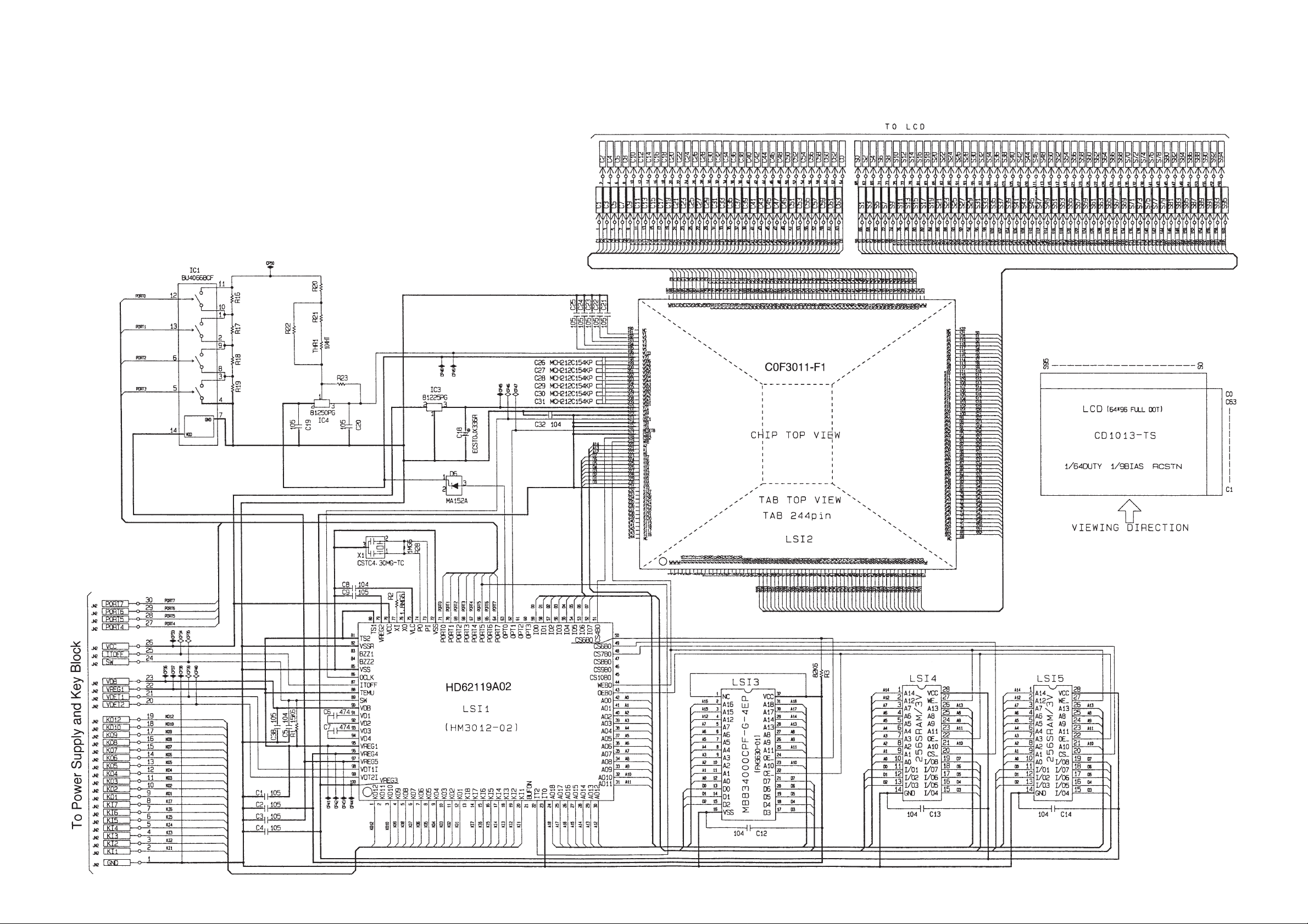
1. SCHEMATIC DIAGRAM
1-1. Main PCB
NOTES
1. The terminals with mark are the checking
points for the power supply.
2. The terminals with mark are the checking
points for the function.
3. LSI5 and C14 are not used.
— 1 —
Page 4
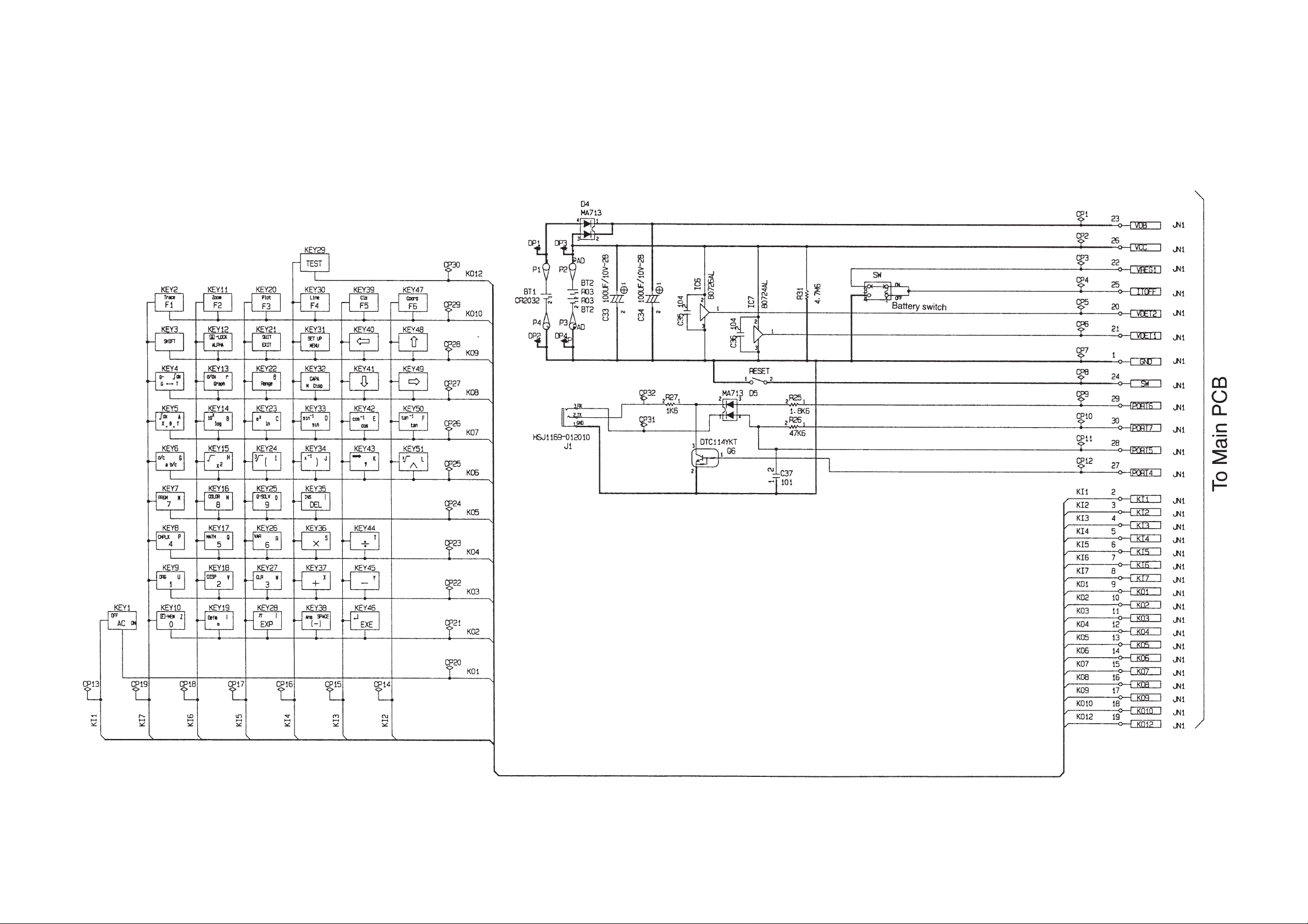
1-2. Power Supply and Key Block
— 2 —
Page 5
2. SPECIFICATIONS
Display system: Three colors (orange, blue, green); 16-character × 8-line liquid crystal
display; 10-digit mantissa and 2-digit exponent for calculations; displays
binary, octal, hexadecimal, sexagesimal values, fraction, complex
number
Power supply: Main: Two AAA-size batteries (LR03 (AM4) or R03 (UM-4))
Memory protection: One CR2032 lithium battery
Power consumption: 0.1W
Battery life*: Main: Approximately 120 hours (continuous display of initial screen.) with
battery type LR03 (AM4)
Approximately 80 hours (continuous display of initial screen.) with
battery type R03 (UM-4)
Approximately 2 years (power switch off) with LR03 (AM4)/R03
(UM-4)
Memory protection: Approximately 2 years
* The batteries that have been installed in this unit when user purchased
it had been used in the factory test, so it will be impossible to fully satisfy
this specifications when these batteries are used.
Auto power off: Power is automatically switched off approximately six minutes after last
operation except when drawing dynamic graphs.
Ambient temperature range: 0°C ~ 40°C (32°F ~ 104°F)
Dimensions: 17.4mm H × 95.5mm W × 182.5mm D ( 5/8" H × 33/4" W × 71/8" D)
Weight: 200g (7.1 oz) including batteries
Accessories: Hard case
Current Consumption
TYP [µA] MAX [µA]
ON (MENU) 4610 5530
OFF 15
— 3 —
Page 6
3. GENERAL GUIDE
3-1. Modes
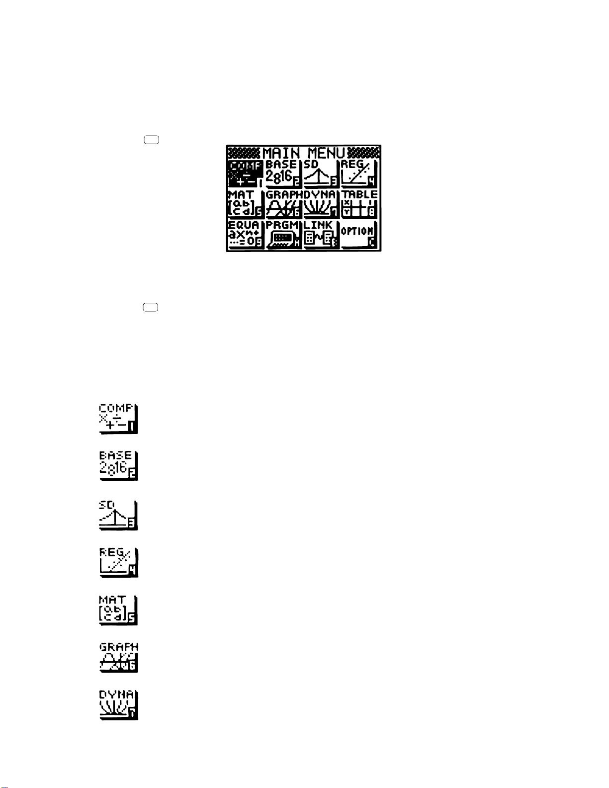
You can control the operations of the unit by entering the correct mode. To select the mode you
need, select the appropriate icon from the Main Menu. The Main Menu appears whenever you
press the
The icon that is highlighted is the one that is currently selected. Use the cursor keys to move the
highlighting around the display to select the mode that you want. To enter the highlighted mode,
press the
• In addition to using the cursor keys to select a mode's icon, you can also select a mode by input-
ting a number or letter. Input the number or letter in the lower right corner of the icon to select the
mode you want.
• Use only the procedures described above to enter a mode. If you use any other procedure, you
may end up in a mode that is different than the one you thought you selected.
MENU
EXE
key.
key.
The following explains the meaning of each icon in the Main Menu.
COMP Mode
Use this mode for arithmetic calculations and function calculations, for drawing graphs
and for executing programs.
BASE Mode
Use this mode for binary, octal, decimal, and hexadecimal calculations and conversions. This mode is also used for logical operations.
SD Mode
Use this mode for single-variable statistical calculations (standard deviation), and for
drawing normal distribution and single-variable statistical graphs.
REG Mode
Use this mode for paired-variable statistical calculations (regression), and for drawing
paired-variable statistical graphs.
MAT Mode
Use this mode for matrix calculations.
GRAPH Mode
Use this mode to input functions and draw their graphs.
DYNA Mode
Use this mode to store graph functions and to draw graphs by changing the values for
variables in the functions.
— 4 —
Page 7
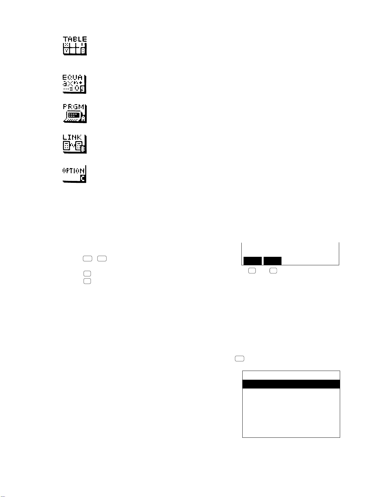
TABLE Mode
Use this mode to store a function or recursion formula, to generate a solution table of
values produced when the values of variables in a function or recursion formula
change, and to draw graphs.
EQUA Mode
Use this mode to solve linear equations with two through six unknowns, quadratic
equations, and cubic equations.
PRGM Mode
Use this mode to store programs in the program area, to execute programs, and to
store and execute programs as file data.
LINK Mode
Use this mode to transfer program, function, matrix, and other memory data to another
unit.
OPTION Mode
Use this mode to adjust the color contrast of the display and to reset the calculator to
its initial settings.
3-2. About Display Colors
The calculator can display data in three colors: orange, blue, and green. The default color for graph
drawing and comment text accompanying a graph or program execution operation is blue, but you
can use the following procedure to change the color to orange or green if you want.
1. Display the Graph Color Menu.
SHIFT
COLOR
F1
(Orn)..Orange graph and comment text
F2
(Grn)..Green graph and comment text
2. Press the function key that correspond to the color you want to specify for graph drawing and
comment text, and then input the text.
3. Execute the function or run the program to display the graph and comment text in the color you
specify.
Orn Grn
F1 F2
3-3. Color Contrast Adjustment
Highlight the OPTION icon on the Main menu and then press
EXE
.
OPTION
COLOR CONTRAST
RESET
TO SELECT: [ ↓ ][ ↑ ]
TO SET : [EXE]
— 5 —
Page 8
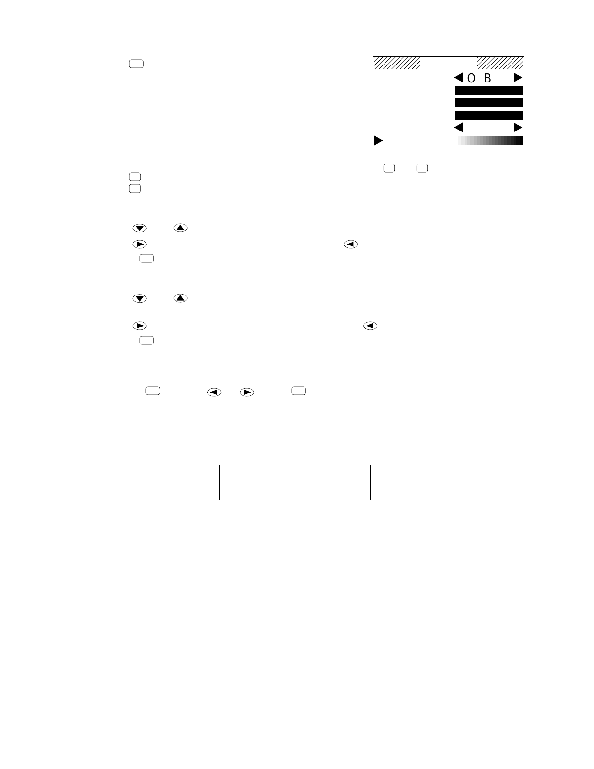
EXE
COLOR
O B G
ORANGE
BLUE
GREEN
– +
CONTRAST
INIT IN·A
F1
(INIT). Returns tint to default setting.
F2
(IN·A). Returns tint and contrast to default setting.
• To adjust the contrast
1. Use and to move the pointer to CONTRAST.
2. Use to make the figures on the display darker or to make them lighter.
3. Press
• To adjust the tint
1. Use and to move the pointer to the color you want to adjust (ORANGE, BLUE,
GREEN).
2. Use to move the setting toward the G (green) side or to move it to the O (orange) side.
3. Press
• When adjusting the color contrast, first adjust overall display contrast, and then adjust the tint of
each individual color.
• You can also adjust the overall contrast whenever any other screen is shown on the display by
pressing
MENU
to return to the Main Menu.
MENU
to return to the Main Menu.
SHIFT
and then or . Press
SHIFT
again to exit the contrast adjustment procedure.
F1 F2
3-4. About Low Battery Warning
If the following message appears on the display, immediately stop using the calculator and replace
batteries.
✽✽ Low battery! ✽✽
If you try to continue using the calculator, it will automatically switch power off, in order to protect
memory contents. You will not be able to switch power back on until you replace batteries.
Be sure to replace batteries at least once every two years, no matter how much you use the calculator during that time.
4.REPLACING BATTERIES
Warning!
If you remove both the main power supply and the memory back up batteries at the same time, all
memory contents will be erased.
— 6 —
Page 9
Precautions:
Incorrectly using batteries can cause them to burst or leak, possibly damaging the interior of the
unit. Note the following precautions:
• Be sure that the positive + and negative - poles of each battery are facing in the proper direc-
tions.
• Never mix batteries of different types.
• Never mix old batteries and new ones.
• Never leave dead batteries in the battery compartment.
• Remove the batteries if you do not plan to use the unit for long periods.
• Never try to recharge the batteries supplied with the unit.
• Do not expose batteries to direct heat, let them become shorted, or try to take them apart.
4-1. To Replace the Main Power Supply Batteries
* Never remove the main power supply and the memory back up batteries from the unit at the same
time.
* Be sure to switch the unit off before replacing batteries. Replacing batteries with power on will
cause data in memory to be deleted.
* Never replace the main power supply battery compartment cover or switch the calculator on while
the main power supply batteries are removed from the calculator or not loaded correctly. Doing so
can cause memory data to be deleted and malfunction of the calculator. If mishandling of batteries causes such problems, correctly load batteries and then perform the RESET operation to
resume normal operation.
* Be sure to replace all two batteries with new ones.
1 Switch the power of the calculator off, and slide the calcula-
tor into its hard case.
2 Remove screw A on the back of the calculator, and remove
the main battery compartment cover.
3 Remove the two old batteries.
4 Load a new set of two batteries, making sure that their
positive + and negative - ends are facing in the proper
directions.
5 Insert the tabs of the main battery compartment cover into
the slots in the back of the calculator and replace the cover.
Secure it in place with the screw.
ON
• Power will not switch on if you press
AC/
while the main
power supply battery compartment cover is open.
ON
6 Remove the calculator from its hard case and press
AC/
to
switch power on.
• Power supplied by memory back-up batteries while the
main power supply batteries are removed retains memory
contents.
• Do not leave the unit without main power supply batteries
loaded for long periods. Doing so can cause deletion of data
stored in memory.
Screw A
— 7 —
Page 10
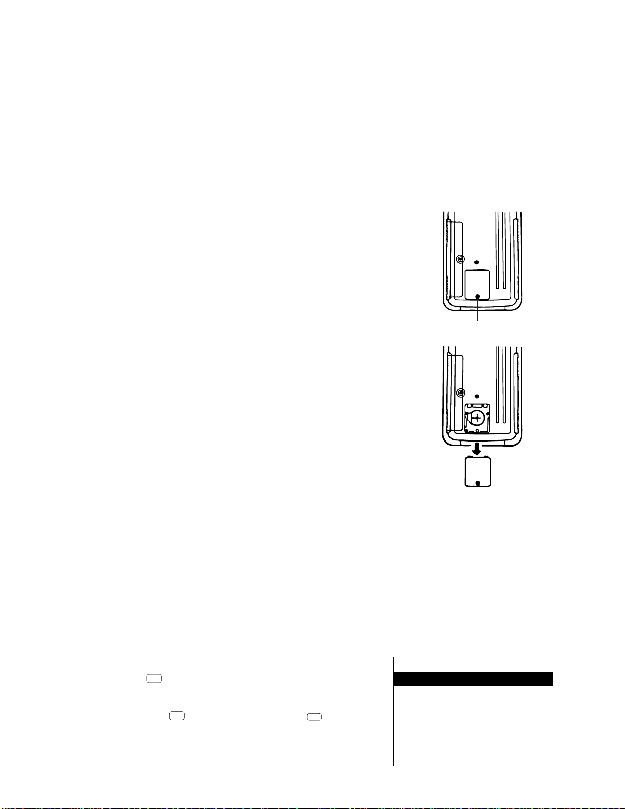
4-2. To Replace the Memory Back Up Battery
OPTION
TO SELECT: [ ↓ ][ ↑ ]
TO SET : [EXE]
COLOR CONTRAST
RESET
* Before replacing the memory backup battery, switch on the unit and check to see if the "Low
battery!" message appears on the display. If it does, replace the main power supply batteries
before replacing the back up power supply battery.
* Never remove the main power supply and the memory back up batteries from the unit at the same
time.
* Be sure to switch the unit off before replacing batteries. Replacing batteries with power on will
cause data in memory to be deleted.
* Be sure to replace the back up power supply battery at least once 2 years, regardless of how
much you use the unit during that time. Failure to do so can cause data in memory to be deleted.
1 Switch the power of the calculator off.
2 Remove screw B on the back of the calculator, and remove
the back-up battery compartment cover.
3 Remove the old battery.
4 Wipe off the surfaces of a new battery with a soft, dry cloth.
Load it into the calculator so that its positive + side is
facing up.
5 Insert the tabs of the back-up battery compartment cover
into the slots in the back of the calculator and replace the
cover. Secure it in place with the screw.
Screw B
6 Switch the power of the calculator on and check for proper
operation.
5. RESET OPERATION
Warning!
The procedure described here clears all memory contents. Never perform this operation unless you
want to totally clear the memory of the calculator.
You should perform the RESET operation whenever you want to initialize the calculator. If you need
the data currently stored in memory, be sure to write it down somewhere before performing the
RESET operation.
• To reset the calculator
1 Switch the power of the calculator on.
2 Press
MENU
to display the Main Menu.
3 Use the cursor keys to select the OPTION icon and
then press
the Main Menu is displayed.
EXE
. Or you can simply press
c
In
— 8 —
while
Page 11

4Use to select RESET and then press
EXE
.
✽✽✽✽✽✽✽✽✽✽✽✽✽✽✽✽✽
✽
RESET
✽
✽✽✽✽✽✽✽✽✽✽✽✽✽✽✽✽✽
RESET
ALL MEMORIES?
RESET ALLN OYES
F1
5Press
6After you finish the RESET operation, adjust the color contrast.
Resetting the calculator initializes the unit to the following settings.
F1
(YES) to reset the calculator, or
F1
(YES)
Item
Mode
Unit of Angular Measurement
Norm
BASE-N
Value Memories
F6
(NO) to abort the reset operation.
Initial Setting
✽✽✽✽✽✽✽✽✽✽✽✽✽✽✽✽✽
✽
✽
RESET
✽
✽
ALL MEMORIES!
✽
✽
✽
✽
✽
✽
✽
✽✽✽✽✽✽✽✽✽✽✽✽✽✽✽✽✽
COMP
Deg
Norm 1
Dec
Clear
✽
Expanded Memory
Function Memory
Ans Memory
Graphic Display
Text Display
Equation Memory
Statistical Data Memory
Matrix Memory
Graphic Function Memory
Dynamic Graph Functions
Table & Graph Data
Input Buffer
Program/File Memory
Clear
Clear
Clear
Clear
Clear
Clear
Clear
Clear
Clear
Clear
Clear
Clear
Clear
— 9 —
Page 12

• Be sure to always keep written copies of all important data in case
you accidently delete it using the RESET operation.
• If the calculator stops operating correctly for some reason, use a
thin, pointed object to press the RESET button on the back of the
calculator. This should make the RESET confirmation screen
appear on the display. Perform the procedure described above to
complete the RESET operation.
• If the RESET confirmation screen does not appear when you press
the RESET button, keep pressing the button until it does.
RESET button
6. WELDING CONDITION FOR THE CERAMIC OSCILLATOR (CSTC4.30MG-TC)
Because the heat-resisting test for welding the ceramic oscillator (CSTC4.30MG-TC) was administered by factory under the condition that weld temperature was 240 ± 5 °C and welding time was 3 ±
1 seconds after the preheating of 150 ± 30 °C temperature and 60 seconds time, it is recommended
that you should give first priority to take the welding condition, 150 ± 30 °C and 60 seconds for
preheating, and 230 ± 5 °C and less 20 seconds for welding, if you have to weld the ceramic oscillator (CSTC4.30MG-TC).
7. ERROR MESSAGE
Message
Syn ERROR
Ma ERROR
Go ERROR
Meaning
1 Calculation formula contains an error.
2 Formula in a program contains an
error.
1 Calculation result exceeds calculation
range.
2 Calculation is performed outside the
input range of a function.
3 Illogical operation (division by zero,
etc.)
4 Poor precision in Σ calculation results.
5 Poor precision in differential calcula-
tion results.
6 Poor precision in integration calcula-
tion results.
7 Cannot find results of equation calcula-
tions.
1 No corresponding Lbl n for Goto n.
2 No program stored in program area
Prog n.
Countermeasure
1 Use or to display the point
where the error was generated and
correct it.
2 Use or to display the point
where the error was generated and
then correct the program.
1234
Check the input numeric value and
correct it.
When using memories, check that the
numeric values stored in memories are
correct.
5 Try using a smaller value for ∆x (x
increment/decrement).
6 Try using a larger value for n (number
of partitions).
7 Check the coefficients of the equation.
1 Correctly input a Lbl n to correspond to
the Goto n, or delete the Goto n if not
required.
2 Store a program in program area Prog
n, or delete the Prog n if not required.
— 10 —
Page 13

Message
Defm
Meaning
Countermeasure
Ne ERROR
Stk ERROR
Mem ERROR
• Nesting of subroutines by Prog n exceeds 10 levels.
• Execution of calculations that exceed
the capacity of the stack for numeric
values or stack for calculations.
1 Specified expanded value memory
does not exist.
2 Not enough memory to expand value
memories specified number.
3 Not enough memory to input a function
into function memory.
4 Not enough memory to create a matrix
using the specified dimension.
5 Not enough memory to hold matrix
calculation result.
6 Not enough memory to store statistical
data.
7 Not enough memory to input coeffi-
cient for equation.
8 Not enough memory to hold equation
calculation result.
9 Not enough memory to hold function
input in the Graph Mode for graph
drawing.
0 Not enough memory to hold function
input in the DYNA Mode for graph
drawing.
A Not enough memory to hold function or
recursion input in the TABLE Mode.
• Ensure that Prog n is not used to return
from subroutines to main routine. If
used, delete any unnecessary Prog n.
• Trace the subroutine jump destinations
and ensure that no jumps are made
back to the original program area.
Ensure that returns are made correctly.
• Simplify the formulas to keep stacks
within 10 levels for the numeric values
and 26 levels for the calculations.
• Divide the formula into two or more
parts.
1 Use
SHIFT
to correctly expand the
number of value memories.
234567890A
• Keep the number of value memories
you use for the operation within the
number of value memories currently
available.
• Simplify the data you are trying to store
to keep it within the available memory
capacity.
• Delete no longer needed data to make
room for the new data.
Arg ERROR
Dim ERROR
Incorrect argument specification for a
command that requires an argument.
• Illegal dimension used during matrix
calculations.
— 11 —
Correct the argument.
• Sci n, Fix n: n = integer from 0 through
9.
• Lbl n, Goto n: n = integer from 0 through
9.
• Prog n: n = 0 through 9, A through Z, r,
θ
.
• Defm n: n = integer from 0 up to the
number of remaining bytes.
• Check matrix dimension.
Page 14

Message
Meaning
Countermeasure
TRANSMIT
ERROR!
RECEIVE
ERROR!
MEMORY
FULL!
Problem with cable connection or parameter setting during data communications.
Problem with cable connection or parameter setting during data communications.
Memory of receiving unit became full
during program data communications.
8.OPERATION CHECK
STEP
1
Use a thin and pointed object to
press the RESET button on the
back of the unit.
OPERATION
•Check cable connection.
•Check to see that the parameters of the
sending unit and receiving unit are
identical.
•Check cable connection.
•Check to see that the parameters of the
sending unit and receiving unit are
identical.
•Delete some data stored in the receiving unit and try again.
DISPLAY
✽✽✽✽✽✽✽✽✽✽✽✽✽✽✽✽✽✽✽✽
✽✽
RESET
NOTE
Reset
✽✽✽✽✽✽✽✽✽✽✽✽✽✽✽✽✽✽✽✽
RESET
ALL MEMORIES?
RESET ALLYES NO
F1
2
✽✽✽✽✽✽✽✽✽✽✽✽✽✽✽✽✽✽✽✽
✽
✽
RESET
ALL MEMORIES !
✽
✽
✽✽✽✽✽✽✽✽✽✽✽✽✽✽✽✽✽✽✽✽
SHIFT
3
RUN / COMP
G-type
Angle
Display
M-D/Cpy
: REC/CON
: Deg
: Nrm1
: M-Disp
ZM PLT LIN CLS
AC/ON
4
ab/c
AC/ON
keys at same
Press
5
F6
LX392 TEST MODE
time.
6
7
1
EXE
No color, no display
(OFF)
1. LCD
2. KEY
3. RAM
4. ROM
5. DET
6. TRS
7. Cnt
0. Rst
Frame is displayed
TEST mode menu
Check for display
Check for display
EXE
8
EXE
9
Red dots are displayed
Green dots are displayed
— 12 —
Check for display
Check for display
Page 15

STEP
Four colors are displayed
Blue
No color
Orange
Green
LX392 TEST MODE
1. LCD
2. KEY
3. RAM
4. ROM
5. DET
6. TRS
7. Cnt
0. Rst
LX392 TEST MODE
1. LCD
2. KEY
3. RAM
4. ROM
5. DET
6. TRS
7. Cnt
0. Rst
LX392 TEST MODE
1. LCD
2. KEY
3. RAM
4. ROM
5. DET
6. TRS
7. Cnt
0. Rst
OPERATION
DISPLAY
NOTE
10
11
12
13
14
15
EXE
EXE
EXE
EXE
EXE
EXE
Blue dots are displayed
Checkers are displayed
Reverse checkers are displayed
Four colors are displayed
Blue
No color
Green
Orange
Check for display
Check for display
Check for display
Color check.
If the colors do not
appear accurately,
please take the
adjustment mentioned in the
section 9.
Color check
TEST mode menu
16
17
18
19
20
21
2
F1
······
4
EXE
3
F2
EXE
Trace
F3
······
Zoom, Plot, Line, ······
Check for keys
Check for keys.
To push the key
sequentially that is
being appeared in
the display.
TEST mode menu
ROMSIZE 4M byte
ROM check
ROM OK
TEST mode menu
RAMSIZE 64K byte
RAM check
RAM OK
RAM2 OK
— 13 —
Page 16

STEP
OPERATION
DISPLAY
NOTE
22
EXE
LX392 TEST MODE
1. LCD
2. KEY
3. RAM
4. ROM
23
0
✽✽✽✽✽✽✽✽✽✽✽✽✽✽✽✽✽✽✽✽
✽✽
RESET
✽✽✽✽✽✽✽✽✽✽✽✽✽✽✽✽✽✽✽✽
RESET
ALL MEMORIES?
RESET ALLYES NO
24
F1
✽✽✽✽✽✽✽✽✽✽✽✽✽✽✽✽✽✽✽✽
✽
✽
RESET
ALL MEMORIES !
✽✽✽✽✽✽✽✽✽✽✽✽✽✽✽✽✽✽✽✽
SHIFT
25
AC/ON
(OFF)
9.COLOR ADJUSTMENT ON OPERATION CHECK
TEST mode menu
5. DET
6. TRS
7. Cnt
0. Rst
Reset
✽
✽
End
STEP
1
2
3
4
5
OPERATION
Use thin and pointed object to
press the RESET button on the
back of the unit.
F1
SHIFT
AC/ON
F6
ab/c
Press
AC/ON
keys at
same time.
DISPLAY
✽✽✽✽✽✽✽✽✽✽✽✽✽✽✽✽✽✽✽✽
✽✽
RESET
NOTE
Reset
✽✽✽✽✽✽✽✽✽✽✽✽✽✽✽✽✽✽✽✽
RESET
ALL MEMORIES?
RESET ALLYES NO
✽✽✽✽✽✽✽✽✽✽✽✽✽✽✽✽✽✽✽✽
✽
✽
RESET
ALL MEMORIES !
✽
✽
✽✽✽✽✽✽✽✽✽✽✽✽✽✽✽✽✽✽✽✽
RUN / COMP
G-type
Angle
Display
M-D/Cpy
: REC/CON
: Deg
: Nrm1
: M-Disp
ZM PLT LIN CLS
(OFF)
LX392 TEST MODE
1. LCD
2. KEY
3. RAM
4. ROM
5. DET
6. TRS
7. Cnt
0. Rst
TEST mode menu
— 14 —
Page 17

STEP
+–
ORANGE
BLUE
GREEN
CONTRAST
COLOR
IN.AINIT
O B G
+–
CONTRAST
COLOR
IN.AINIT
O B G
LX392 TEST MODE
1. LCD
2. KEY
3. RAM
4. ROM
5. DET
6. TRS
7. Cnt
0. Rst
OPERATION
DISPLAY
NOTE
6
7
COLOR
ORANGE
O B G
Color adjustment
mode
BLUE
GREEN
+–
CONTRAST
IN.AINIT
7
Aim at the
CONTRAST
8
or
Adjust the color
until the primary
colors appear
accurately.
9
10
EXIT
Take the steps as same as the
end of OPERATION CHECK to
end this adjustment.
TEST mode menu
End
— 15 —
Page 18

10. DATA TRANSFER CHECK
F6
AC/ON
Turn off both units and connect them by using the cable SB-60.
STEP
1
2
3
4
5
6
MASTER
OPERATION DISPLAY
F6
ab/c
Press
AC/ON
LX392 TEST MODE
keys at same
time.
1. LCD 5. DET
2. KEY 6. TRS
3. RAM 7. Cnt
4. ROM 0. Rst
6
TRANSMIT Check
1. COM Check
2.
Random Data Out
1
0. Self
1. Send
2. Receive
1
SENDING
COM END
EXE
0. Self
1. Send
2. Receive
OPERATION
Press
ab/c
keys at same
time.
6
1
2
EXE
SLAVE
DISPLAY
LX392 TEST MODE
1. LCD 5. DET
2. KEY 6. TRS
3. RAM 7. Cnt
4. ROM 0. Rst
TRANSMIT Check
1. COM Check
2.
Random Data Out
0. Self
1. Send
2. Receive
WAITING
WAITING
COM OK
0. Self
1. Send
2. Receive
NOTE
TEST mode
menu
Check for
sending
2
7
8
EXE
9
10
11
AC/ON
Take the steps as
same as the end
of OPERATION
CHECK to end
this check.
WAITING
WAITING
COM OK
0. Self
1. Send
2. Receive
LX392 TEST MODE
1. LCD 5. DET
2. KEY 6. TRS
3. RAM 7. Cnt
4. ROM 0. Rst
1
EXE
Take the steps as
same as the end
of OPERATION
CHECK to end
this check.
SENDING
COM END
0. Self
1. Send
2. Receive
LX392 TEST MODE
1. LCD 5. DET
2. KEY 6. TRS
3. RAM 7. Cnt
4. ROM 0. Rst
Check for
receptivity
TEST mode
menu
End
— 16 —
Page 19

11. DATA COMMUNICATIONS
• Though you can transfer programs between the CFX-9800G and another CFX-9800G, an fx7700GB, an fx-7700GE an fx-7700GH, an fx-9700GE, an fx-9700GH, an OH-7700GE, an OH9700GE or an fx-8700GB, all of the examples in this manual cover data transfer with another
CFX-9800G only.
11-1. Connecting Two CFX-9800G Units
The following procedure describes how to connect two Power Graphic units with an optional SB-62
connecting cable for transfer of programs between them.
To Connect Two CFX-9800G Units
1. Check to make sure that the power of both CFX-9800G units is off.
2. Remove the covers from the connectors of the two Power Graphic units.
• Be sure you keep the connector covers in a safe place so you can replace them after you
finish your program communications.
3. Connect the two units using the SB-62 cable.
SB-62 cable
Important
• Keep the connectors of the CFX-9800G covered when you are not using them.
11-2. Before Starting Data Communications
Before actually starting data communications, you should first enter the LINK Mode from the Main
Menu.
To Enter the LINK Mode
Highlight the LINK icon on the Main Menu.
Press
The following are the operations that can be selected from the function menu at the bottom of the
display. Press the function key below the operation you want to perform.
EXE
to display the LINK Mode.
EXE
F1
(TRN) .............Transmit
F2
(RCV) .............Receive
F6
(SET) ............. Set up display
COMMUNICATION
PARITY : EVEN
BPS
M–D/Cpy
TRN
: 9600
: M–Disp
RCV SET
F1 F2 F6
— 17 —
Page 20

About the Data Type Selection Screen
F2
Whenever you press F1 (TRN) to send data or F2 (RCV) to receive data, a data type selection
screen appears on the display.
Send Unit Receive Unit
F1
(TRN)
(RCV)
TRANSMIT DATA
ALL
Program
Editor
Function Memory
Matrix
Statistics
Variable Memory
RECEIVE DATA
ALL
Program
Editor
Function Memory
Matrix
Statistics
Variable Memory
Pointer Indicates more below
The following table describes what each of these items means. You will learn later how to make a
selection using these screens.
Selection Meaning
ALL All data from Program to Equation
Program Program data
Editor File names and file data
Function Memory Function memory contents
Matrix Matrix memory contents
Statistics Single-variable and paired-variable statistical data
Variable Memory Value memory and extended memory contents
Range Graph range parameters
Factor Factor function zoom ratios
Table Table & Graph function data
Graph Function Graph functions, graph draw/non-draw specifica-
tion, graph color specification.
Dynamic Graph Dynamic Graph function data
Equation Equation coefficients
Back Up All memory contents, including mode settings
Note
• If the selections you make on the send unit and receive unit do not match, a TRANSMIT ERROR
will be generated on the sender and a RECEIVE ERROR will be generated on the receiver.
11-3. Setting Communications Parameters
Before you can perform data communications, you must first set up certain hardware parameters to
make sure that the two units are able to understand each other. The parameters of the sender and
the receiver must be identical for them to be able to communicate correctly. There are two hardware
parameters that you can set.
Parameter Settings
EVEN
PARITY ODD
NONE
1200
Speed (BPS)
— 18 —
2400
4800
9600
Page 21

To Set CFX-9800G Parameters
12
F1 F2 F3
BPS : 9600
24 48 96
<×100>
F4
EVN ODD NON
PARITY : EVEN
BPS
: 9600
M–D/Cpy
: M–Disp
F1 F2 F3
RECEIVE DATA
ALL
Program
Editor
Function Memory
Matrix
Statistics
Variable Memory
= = RECEIVE = =
ALL DATA
YES
NO
F1 F6
F2
Starting from the LINK Mode:
SHIFT
F6
(SET) (or
SET UP
)
• This display shows the currently set parameters.
Press the function key that corresponds to the parity you want to set.
Press to select BPS.
Press the function key that corresponds to the communication speed you want to set.
Press
EXIT
to complete the procedure and return to the previous function menu.
11-4. Using ALL, Range, and Factor
The following procedures show how to send data using ALL, Range, and Factor from one CFX9800G unit to another. The example procedure shows an operation using ALL only, but the procedures for Range and Factor are identical.
• To send data using ALL
Send Unit
Starting from the LINK Mode, press the function
key to enter the send mode.
F1
(TRN)
TRANSMIT DATA
ALL
Program
Editor
Function Memory
Matrix
Statistics
Variable Memory
Make sure that the pointer is located at ALL, and
EXE
press
EXE
to specify it as the data type.
= = TRANSMIT = =
ALL DATA
Starting from the LINK Mode, press the function key
to enter the receive mode.
(RCV)
Make sure that the pointer is located at ALL, and
EXE
press
EXE
to specify it as the data type.
Receive Unit
Press F1 (YES) to start the send operation, or
(NO) to abort without sending anything.
YES
F1 F6
NO
F6
Press F1 (YES) to start the receive operation, or
(NO) to abort without receiving anything.
— 19 —
F6
Page 22

F1
COMMUNICATION
COMPLETE
ALL DATA
PRESS [ AC ]
= = RECEIVING = =
ALL DATA
TO STOP : [ AC ]
(YES)
= = TRANSMITTING = =
ALL DATA
TO STOP : [ AC ]
F1
(YES)
* Pressing AC interrupts the send operation and
returns to the LINK Mode.
The following appears after the send operation is
complete.
COMMUNICATION
COMPLETE
ALL DATA
PRESS [ AC ]
* Pressing AC interrupts the receive operation and
returns to the LINK Mode.
The following appears after the receive operation is
complete.
* Press AC to return to the LINK Mode.
Warning!
Transferring data using ALL causes data in the applicable memory areas of the receiving unit to be
replaced by the received data. Make sure that you do not need the data stored in the receiving unit
before you start an operation using ALL.
11-5. Data Communications Precautions
Note the following precautions whenever you perform data communications.
• A TRANSMIT ERROR occurs whenever you try to send data to a receiving unit that is not yet
standing by to receive data. When this happens, press AC to clear the error and try again, after
setting up the receiving unit to receive data.
• A RECEIVING ERROR occurs whenever the receiving unit does not receive any data approximately six minutes after it is set up to receive data. When this happens, press AC to clear the
error.
• A TRANSMIT ERROR or RECEIVE ERROR occurs during data communications if the cable
becomes disconnected, if the parameters of the two units do not match, or if any other communications problem occurs. When this happens, press AC to clear the error and correct the problem
before trying data communications again. In this case, any data received before the problem
occurred is cleared from the receiving unit's memory.
• A MEMORY FULL operation occurs if the receiving unit memory becomes full during data communications. When this happens, press AC to clear the error and delete unneeded data from the
receiving unit to make room for the new data, and then try again.
— 20 —
Page 23

12. PIN FUNCTION
12-1. CPU (HD62119A02)
Pin No. Pin Name Input / Output Function
1,3~12 KO1~KO10,KO12 O Key common signal
14~20 KI1~KI7 I Key input signal
2 2 IT2 I Interrupt input
23 IT0 GND
24~42 AO0~AO18 O Address bus
43 OEBO O Enable signal
4 4 WEBO O Enable signal to write
48~51 CS4BO~CS7BO O Chip selecting signal
52~59 IO0~IO7 I Data bus
62,63 OPT0,OPT1 O Output point for check
64~71 PORT0~PORT7 I/O Input/output point
72 VSS GND
73,74 PI,PO Power for ceramic oscillator
7 5 VLC Power
76,77 XO,XI Power
78 VCC Power for LSI
79 VREG2 Power
80,81 TS1,TS2 I Terminal for test
82 VSSR GND
85 VSS GND
86 OCLK O Clock
87 ITOFF I/O Terminal for power switch
89 SW I Reset switch
9 0 VDB Power
91~94 VD1~VD4 Power for doubler
95 VREG1 Regulator power for LSI
96 VREG4 Regulator power for ROM
97 VREG5 Regulator power
98,99 VDT1I,VDT2I I Terminal for detector
100 VREG3 Regulator power for RAM
— 21 —
Page 24

12-2. ROM (MB834000CPF-G-4EP)
Pin No. Pin Name Input / Output Function
1 NC I Power supply
2~12,23,25~31, A0~A18 I Address input
13~15,17~21 D0~D7 O Data output
16 VSS I Ground
22 CE I Chip enable input from CPU
24 OE I Output enable input from CPU
32 VCC I Power supply
12-3. RAM (256SRAM/3V)
Pin No. Pin Name Input / Output Function
1~10,21,23~26, A0~A14 I Address input
11~13,15~19 IO1~IO8 I/O Data input/output
1 4 GND I Ground
20 CS I Chip select signal
22 OE I Output enable input from CPU
27 WE I Write enable input
28 VCC I Power supply
— 22 —
Page 25

13. TROUBLESHOOTING
SYMPTOM CAUSE SOLUTION
Intermittent display
No display at all
Erratic display
Dirt or poor contact on battery
Poor contact on power switch
Poor connection on PC joiner
Poor soldering on LSI, capacitor, or resistor
Weak battery
Dirt or poor contact on battery
Poor contact on power switch
Poor connection on PC joiner
Defective LSI, capacitor, or resistor
Poor contact between LCD and PCB
Poor soldering on LSI
Clean or adjust pressure of
contact
Clean or replace power
switch
Resolder or replace
Resolder
Replace battery
Clean or adjust pressure of
contact
Clean or replace power
switch
Resolder or replace
Replace
Replace the heat seal
Resolder or replace display
PCB ass'y
Certain key does not
function
All keys do not function
Heavy key motion
Dirt on key contact
Heavy key motion
Poor soldering on LSI
Defective LSI, capacitor, or resistor
Constant contact is made on a certain key
Defective LSI, capacitor, or resistor
Dirt or scratch on the key
Clean or replace contact
Clean or replace the key
Resolder
Replace
Separate the contact
Replace
Clean or replace the key
— 23 —
Page 26

14. DISASSEMBLY AND EXPLODED VIEW
1. Loosen both J and M screws on the battery covers K and L after removing the hard case l
from the body, and remove the battery covers and batteries.
2. Loosen the four screws N on the lower case E, and remove this lower case from the body.
3. Remove one end of the PC joiner D from the L392-1 assembly 1 with the help of fusing its
weld.
4. Loosen the two screws j on the L392-1 assembly 1 and the four screws j on the LCD holder
3, then remove the L392-1 assembly 1 from the upper case U.
5. Loosen the six screws j on the L392-2 assembly, and remove the L392-2 assembly from the
upper case U.
— 24 —
Page 27

53
51
5
33
7
31
45
43
44
52
32
36
42
41
35
34
32
12
50
8
40
50
47
50
4
2
37
13
27
26
25
19
29
27
28
16
17
30
14
5
15
28
10
46
48
38
49
39
11
50
— 25 —
18
54 55
6
3
56 57
24
22
21
23
20
Page 28

Obverse side Reverse side
1
10 11
9
5
7
6
2
3
4
5
8
14
13
Fig. 1. L392-1 assembly and L392-2 assembly.
12
C33
C34
J1
— 27 —
Page 29

15. PARTS LIST
FOB Japan
N Item Code No. Parts Name Specification Q M N.R.Yen R
Unit Price
L392-1 ASS'Y
N 1 6413 4940 PCB L392-1 Ass'y A140050*1
(This assembly contains the following available elements.)
1A
1
N LSI1 2012 0546 LSI HD62119A02
N LSI3 2012 0406 LSI MB834000CPF-G-4EP
LSI4 2011 3955 LSI UPD43256BGU-B12
IC1 2105 3213 C-MOS IC BU4066BCF-T1
N IC3 2105 4235 C-MOS IC XC62AP2502PR
N IC4 2105 2737 C-MOS IC RH5RL50AA-T1
X1 2590 1967
C1~4,C9, 2845 1925 Chip capacitor MCH312F105ZP
C19~25,C38
C5,C8,C12, 2845 2548 Chip capacitor MCH183F104ZK
C13,C32
C6,C7 2895 1365 Chip capacitor MCH325F474ZP
C18 2895 2359 Chip tantalum capacitor ECSTOJX336R
C26~31 2845 5684 Chip capacitor MCH212C154KP
D6 2390 1260 Chip diode MA152A-(TX)
R1 2791 1595 Chip resistor ERJ-6GEYJ153V
R2 2795 5649 Chip resistor MCR10EZHG185
R3 2797 0252 Chip resistor ERJ-6GEYJ823V
N R16 2797 4214 Chip resistor ERJ-6ENF1001V
N R17 2797 4221 Chip resistor ERJ-6ENF2001V
N R18 2797 4228 Chip resistor ERJ-6ENF4021V
N R19 2797 4235 Chip resistor ERJ-6ENF8061V
N R20 2797 4403 Chip resistor ERJ-6ENF9312V
R21 2797 4032 Chip resistor ERJ-6ENF1502V
N R22 2797 4256 Chip resistor ERJ-6ENF9762V
N R23 7102 6064 Chip resistor ERJ-6ENF1003V
R28 2797 0616 Chip resistor ERJ-6GEYG105V
N THR1 2755 0147 Thermistor 104HT
N 2 3335 5558 LCD CD1013-TS
N 3 6413 5160 LCD holder L392 A340165-1
N 4 6413 5200 Tape B-L392 A440299-1
5 6403 9330 Tape C-L170 A413108-1
N 6 5610 8300 Heat seal B-L392 A340116-1
N 7 6413 5210
N 8 6413 5180 Cushion A-L392 A440250-1
N 9 6413 5320 COF3011-F1 sub ass'y A340214*1
N 10 5610 8290 Heat seal A-L392 A340113-1
N 11 6413 5171 Adhesive tape B-L392 A440249A-1
L392-2 ASS'Y
N 12 6413 4960 PCB L392-2 Ass'y A240063A*1
(This assembly contains the following available elements.)
Ceramic oscillator
Cushion B-L392
CSTC4.30MG-TC
A440322-1 1 20 X
1C
1
1C
1
1C
1
10 C
1
5C
1
10 C
1
5C
1
10 C
13
20 C
5
10 C
2
10 C
1
20 C
6
20 C
1
20 C
1
20 C
1
20 C
1
20 C
1
20 C
1
20 C
1
20 C
1
20 C
1
20 C
1
20 C
1
20 C
1
20 C
1
5C
1
1A
1
20 C
1
20 X
1
20 X
2
1A
1
20 X
1
1C
1
10 A
1
20 C
2
1A
1
N 13 6413 5220 Tape C-L392 A440302-1
N C33,C34 2803 7800 Electriolytic capasitor RE3-10V101M-T58
C35,C36 2845 2548 Chip capasitor MCH183F104ZK
C37 2845 2898 Chip capasitor MCH185A101JK
D4,D5 2390 0364 Schottky diode MA713-TX
N IC6 2105 4242 CMOS IC XC61AC2602PR
Notes: N – New parts R – A : Essential
M – Minimum order/supply quantity B : Stock recommended
R – Rank C : Others
Q – Quantity used per unit X : No stock recommended
— 28 —
20 X
1
20 C
2
20 C
2
20 C
1
10 C
2
10 C
1
Page 30

FOB Japan
N Item Code No. Parts Name Specification Q M N.R.Yen R
Unit Price
N IC7 2105 4074 CMOS IC S-80724AL-AM-T1
J1 3501 6538 Miniature jack HSJ1169-012010
Q6 2259 0959 Chip digital transistor DTC114YKT-146
R25 2792 1191 Chip resistor MCR10EZHJ182
R26 2792 0462 Chip resistor MCR10EZHJ473
R27 2792 0470 Chip resistor MCR10EZHJ102
N R31 2795 5663 Chip resistor MCR10EZHJ475
COMPONENTS
N14
N 15 6413 5300 Lower case L392 A140048-1
N 16 6274 7023 Contact spring A4532C-1
N 17 6413 5310 Switch knob L392 A340089-1
N 18 6411 6700 Battery spring B-L196 A415028-1
19 6398 8940 Battery spring L383 A311808-1
N 20 6413 5110 Flat screw L392 A440276-1
N 21 6413 5050 Battery cover A-L392 A340108-1
N 22 6413 5060 Battery cover B-L392 A340117-1
N 23 6413 6020 Screw B-L392 A412299-10
24 6386 9510 Screw A-V426 A310044-3
25 6329 7660 Battery insuration plate G272 A45154-1
26 6329 7620 Battery spring A-G272 A33938-1
27 6323 1011 Insuration seal G106 A43065-1
N 28 6408 1120 Nut L598AA A411430-4
N 29 6391 8831 Rubber key V160 A311024A-1
30 6405 6440 Blind al171 A413625-1
N 31 6413 5240 Upper case L392 A140035-1
N 32 6413 5280 Adhesive tape D-L392 A440185-3
N 33 6413 5250 Protector L392 A340119-1
N 34 6413 5260 Adhesive tape A-L392 A440185-1
N 35 6413 5290 Display plate L392 A340112-1
N 36 6413 5270 Adhesive tape C-L392 A440185-2
37 6386 7450 Battery spring A-V355 A410112-1
N 38 6413 5000 Button B-L392 A340110-1
N 39 6413 5020 Button D-L392 A340123-1
40 6403 8700 Battery spring C-L180 A412985-1
N 41 6413 5100 Button G-L392 A313257-5
N 42 6413 5010 Button C-L392 A340111-1
43 6408 0080 Button F-L370 A313257-2
44 6408 0070 Button E-L370 A313257-1
N 45 6413 5070 Button B-L392 A211316-4
N 46 6413 4990 Button A-L392 A240072-1
47 6390 0430 Cap V332 A310765-1
N 48 6413 6000 Button H-L392 A340256-1
N 49 6413 5030 Key contact rubber L392 A240061-1
50 6396 7660 Screw A-L564 A310044-13
N 51 6413 5130 Plate L392 A340243-1
N 52 6413 5040 Hard case L392 A240058-1
53 6405 8831 Rubber strip L373 A412232A-2
N 54 6414 0050 FCC Label L392 A440395-1
N 55 6414 4660 EMI Label L392AAC A440566-1
N 56 6413 5120 Label L392 A440354-1
N 57 6414 3730 Label L392AAQ A440354-3
Notes: N – New parts R – A : Essential
6413 6010
OTHERS
M – Minimum order/supply quantity B : Stock recommended
R – Rank C : Others
Q – Quantity used per unit X : No stock recommended
PC joiner L392 A413642-5
— 29 —
10 C
1
5C
1
20 C
1
20 C
1
20 C
1
20 C
1
20 C
1
5C
1
5C
1
20 C
1
20 C
1
10 C
1
20 C
1
20 C
1
20 C
1
20 C
1
20 C
1
20 C
4
20 C
1
20 C
1
20 C
2
20 C
2
20 C
1
20 C
1
1C
1
20 C
2
5C
1
20 C
1
10 C
1
20 C
1
20 C
1
20 C
1
20 C
1
20 C
1
20 C
1
10 C
1
20 C
1
20 C
1
10 C
1
10 C
1
20 B
1
20 C
1
5C
1
20 C
12
1C
1
1C
1
20 C
1
20 X
1
20 X
1
20 X
1
20 X
1
Page 31

8-11-10, Nishi-Shinjuku
Shinjuku-ku, Tokyo 160, Japan
Telephone: 03-3347-4926
 Loading...