

Page 1

HV20 A
TECHNICAL DESCRIPTION
1. Technical Description
1-1 HDMI Terminal
The HV20 A comes with an HMDI (High Definition Multimedia Interface) digital interface terminal for inputting and outputting the
next-generation video, audio and control signals. This is the interface which was developed for digital home appliances and audiovisual
equipment. Using a completely digital system, the HDMI terminal enables the transfer of the video, audio and inter-unit control signals
by means of an easily routable cable provided with small (19-pin) terminals.
When the HDMI terminal on the HV20 A is connected to another display unit, the information on the display unit’s capabilities referred
as the EDID (Extended Display Identification Data) is read by the HV20 A, and the unit’s output format is determined. What happens
next is that the video images and sound best suited to the display unit are transmitted from the HV20 A main unit. This means that there
is now no longer the need to set the TV display mode (normal or wide) to match the display unit to which the HV20 A is connected
something that would be necessary with other terminals.
The HV20 A does not support HDCP (High-Bandwidth Digital Content Protection) for protecting contents from being copied, the CEC
(Consumer Electronics Control) function for exercising reciprocal control between units or color space expansion.
In this way, the standard of the video images output from the HV20 A is determined by the capabilities of the display unit connected to
the HV20 A, and the table below shows the sequence of priority for the output of the HV20 A in terms of each of the display unit’s
capabilities.
Camera body Output 1080i 480i/576i 480i/576i 480P/576P 480P/576P
mode (16:9) (4:3) (16:9) (4:3)
HD 1 2 (*1) 4 (*1) 3 (*2) 5 (*2)
SD (wide) --- 1 3 2 (*3) 4 (*3)
SD (normal) --- 3 1 4 (*3) 2 (*3)
Print screen (HD) --- 1 (*1) 3 (*1) 2 (*2) 4 (*2)
(*1) : Down-conversion, (*2) : IP conversion after down-conversion, (*3) : IP conversion processing
The sound is delivered in one of the linear PCM (Pulse Code Modulation) output formats listed in the table below depending on the
mode of the HV20 A main unit.
Camera body mode Output
SD-12bit/32kHz-2ch/4ch 32kHz-16bit-2ch
SD-16bit/48kHz-2ch 48kHz-16bit-2ch
HD-48Hz-2ch/4ch 48kHz-16bit-2ch
Related specifications
1. When a receiver is connected to the HV20 A main unit using the HDMI terminal, the video output to the component/composite
terminals is forcibly shut down.
2. The audio signals to the AV terminal are output all the time if that terminal has been connected.
3. If a DVI monitor (for a PC) has been connected, RGB signals in the 480P format will be output, but no guarantees are made for
the connections or quality of the images displayed on the monitor.
4. During an HDMI connection, the “TV type” and “Component output” menu settings are grayed out and rendered inoperable.
5. When HDV/DV signals are input or the analog input mode is established, the HDMI output is forcibly shut down.
6. In both the SD and HD modes, the sound can be selected by setting “Audio output” as with the LINE OUT output when a 4channel tape is played back.
7. DVI signals will be output if the EDID of the unit connected to the HV20 A cannot be read, if the EDID which has been read has
been destroyed or if the output format cannot be determined for some other reason.
8. hen a copy-protected tape has been played back, the output signals of the HDMI terminal will be muted, and a warning will be
displayed.
Neither will signals be output to the HDMI terminal when a “copy-disabled” tape on which digital broadcasts have been
recorded with analog input signals is played back.
(At such times, the EVF/LCD will also be muted.)
9. Bilingual audio signals cannot be output to the HDMI terminal.
1
Page 2

HV20 A
TECHNICAL DESCRIPTION
z The status settings can be checked on the menu screen.
(1)When 1920 × 1080i signals are output, “1920 × 1080i” is displayed.
(2)When 720 × 480i signals are output, “720 × 480i” is displayed.
(3)When 720 × 480P signals are output, “720 × 480P” is displayed.
(4)When DVI signals are output, “DVI” is displayed.
(5)When no units have been connected or the output format has not been determined,
“---------” is displayed.
Fig. 1
1-2 New Video Recording Standards
1-2-1 HDV (PF24) and CINE Mode (Each of these modes is effective only while the camera is in the tape mode.)
The HV20 A features some new functions that enable users to take shots with a cine-like quality or that can be applied as full-blown
digital cinema tools.
(1) NTSC : HDV (PF24)
The PF (Progressive Frame)24 setting, which has the same frame rate as cine shooting,
has been added as a video recording standard. (Refer to the figure on the right.) This
enables movie shooting at 24 frames per second which is a rate that takes full advantage
of the progressive readout capability of the CMOS chip.
When this mode is established, real 24P shooting with HD image quality is executed.
In NTSC areas, tapes are recorded in the 60i format using 2:3 pulldown.
(2) CINE mode
Joining the mode in (1) is the “CINE mode” which has been added to enable shooting
at a film image quality .
(FUNC. setting: Refer to the figure on the right.)
When CINE mode is established, the cine gamma, cine matrix and other image quality
adjustments which are based on custom preset 8 (CP8: CINE.V) of the XH G1 A, XH
A1 A are performed. By setting both the cinema mode and the HDV (PF24) mode in
(1), users can achieve images with a cine-like quality during TV viewing.
What’s more, the HDV (PF24) mode and CINE mode can each be set independently:
for instance, users can even set up the image quality of the CINE mode when the HDV/
DV (wide)/DV (normal) setting has been selected. However, this setting is not available in the AUTO mode.
HDV(PF24)
Fig. 2
CINE MODE
Fig. 3
1-3 Improved Operability
On the side panel at the front of the HV20 A main unit are a dedicated focus button for switching between Auto focus and manual
focus and a focus dial for focusing which team up to improve
focusing operations.
The same side panel at the front of the HV20 A main unit has a
backlight correction button (BLC button) for allocating the backlight correction function to make it easier for users to operate the
function using their left hand while they are holding the camera in
their right hand.
Backlight correction button
Focus button
(A/M switching)
Focusing dial
Fig. 4
2
Page 3

TECHNICAL DESCRIPTION
2. PCB Functions
(1) MAIN PCB
System-Control Section
• IC100 CCM MI-COM System control (Camera/Card/Mode)
• IC101 FLASH Flash-ROM for CCM MI-COM (16Mbit)
• IC102 EX-OR GATE Generation of address signals and CS signals
• IC103 AND GATE Pass-ready notification signal between IC100/IC1101 (DIGIC DV II)
and between IC1000 (MPX)
• IC104 MOTOR DRIVER IC Motor drive for barrier
• IC105 NAND GATE Generation of address signals and CS signals
• IC106 EX-OR GATE Generation of address signals and CS signals
• IC107 NOR GATE Generation of address signals and CS signals
• IC108 CHIP SELECT DECODER Generation of address signals and CS signals
• IC109 ANALOG SWITCH MIC communication control
Camera/Card section
• IC1000 MPX4 AGC, image composition, defective pixel compensation, serial/parallel
conversion
• IC1100 DIGIC DV II Camera digital signal processing, card video image processing
• IC1102 SDRAM Memory for DIGIC DV II (128Mbit)
• IC1103 SDRAM Memory for DIGIC DV II (128Mbit)
• IC1200 LENS DRIVER Zoom, focus motor driver, IRIS driver, and gyro output AMP
• IC1501 CVF DRIVER CVF signal processing/driving
Lens section
• IC1611 SHIFT LENS DRIVER IC Driver IC for shift lens drive
• IC1612 D/A CONVERTER 8-bit, 8ch D/A converter for adjusting shift lens, DMC and focus lens
• IC1613 OPE AMP Shift lens positional sensor, sensor amplifier
Video section
• IC2000 VRP2 Record playback head amplifier
• IC2301 VIC HDV Digital VCR signal processing LSI, FR MI-COM,
Analog SD signal input/output processing
• IC2303 1394IC IEEE 1394 digital signal processing (MPEG-2 TS / DV)
• IC2306 OR GATE Serial communication control
• IC2307 SDRAM Memory for video signal processing/recording signal processing
• IC2308 AND GATE Timing adjustment at WRITE access to SRAM
• IC2309 AND GATE Timing adjustment at WRITE access to SRAM
• IC2310 FLASH/SRAM Memory for IC2303
• IC2800 HDV CODEC IC Compression/expansion for video & audio HDV
• IC2801 BASEBAND IC Component/SDI output, HD → SD conversion
• IC2802 COMPONENT DRIVER 75Ω driver AMP for component output
• IC2830 HDMI IC HDMI signal processing
• IC2831 DUAL INVERTER IC For reversing signal logic
• IC2833 PRESET AND CLEAR Signal control
Servo section
• IC300 MOTOR DRIVER IC Drum, capstan, and loading motor driver
PM section
• IC3200 MAIN POWER IC Power DC/DC converter (MAIN)
• IC3260 3.2V REGULATOR 3.2V regulator
• IC3261 4.6V REGULATOR 4.6V regulator
• IC3300 SUB POWER IC Power DC/DC converter (SUB)
• IC3310 5.0V REGULATOR 5.0V regulator
HV20 A
3
Page 4

USB section
• IC3500 USB IC USB I/F
Audio section
• IC801 AIF4 Analog input/output signal processing, speaker amplifier
USB conector
(2) LCD PCB
• IC901 LCD DRIVER LCD signal processing/driving
• IC902 EEPROM EEPROM for LCD parts data
• IC903 2.8V REGULATOR 2.8V regulator
(3) CVF PCB
• IC1691 P SENSOR GYRO Pitch-direction angular velocity detection
• IC1692 Y SENSOR GYRO Yaw-direction angular velocity detection
(4) JACK PCB
• IC501 DC/DC CONVERTER CONTROL FLASH main condenser electric charge control
• IC502 CMOS IC Flash light emission switch drive
HV20 A
TECHNICAL DESCRIPTION
(5) CMOS SENSOR PCB
• IC1040 INVERTER Standard logic inverter
• IC1041 AFE Bch, Rch
• IC1042 AFE Gch
• IC1043 5V REGULATOR 5V regulator
• IC1044 4.2V REGULATOR 4.2V regulator
• IC1045 AMP Operational amplifier
• IC1046 CMOS CMOS image sensor
• IC1047 2.7V REGULATOR 2.7V regulator
(6) LCD PCB
LCD open detection SW, LCD reversing detection SW
(7) REAR PCB
Eject SW
(8) CVF FPC PCB
Display button switch, Easy direct button switch
(9) CARD PCB
Reset SW
(10) MF DIAL FPC PCB
Backlight correction button switch, Focus button switch, Focus dial switch
(11) C COVER ZOOM FPC PCB
Zoom lever switch, Joystick switch, Photo button switch, SET button switch, Power supply switch button, Movie shooting
mode selector switch, Start/stop button switch, Tape/Card selector switch, FUNC button switch
4
Page 5

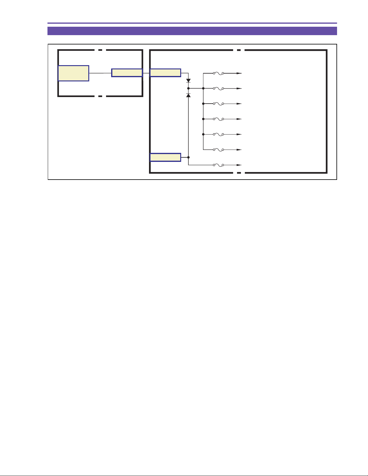
3. Power Supply Circuit
3-1 Startup of Power Supply
HV20 A
TECHNICAL DESCRIPTION
BATTERY WIRE
BATTERY
TERMINAL
+
−
CN1
A16-A23
B13-B20
MAIN PCB
CN3200
+
−
DC JACK
CN3201
A16-A23
B13-B20
DMC-III
CASSETTE
IN SW
12
VCC
2.8V REG.
E3V
B5 A2
IC2301
FR MI-COM.
(VIC HDV)
IC3300
SUB POWER IC
VCC
C1C7
VTR ON
CCM
RESET
E3+LI
IC3200
MAIN POWER IC
LI-POWER
A5
CTL
3
A4
E14
CAS IN
VTR ON IC3300
A13
DC V DET
U10
RESET
G1
VTR ON IC3200
C14
VCC
B RESET
G14
E3V
F9
IC1100
DIGIC DV II
SERIAL
DATA
IC100
CCM
MI-COM.
CN500
B28
B28
CN1
LITHIUM
BATTERY
(2ND)
BATTERY WIRE
Fig. 5
5
Q100
RESET
SW
EJECT SW
EJECT PCB
CAM
POW SW
VTR
EJECT
POW SW
SW
CN1501CN102
CN872
CN873
CN100
POWER SW
D16
526
56
CVF FPC
65
65
D17
CASSETTE COVER
E16
Page 6

TECHNICAL DESCRIPTION
• Backup Lithium Battery
LI3V power from lithium battery is input to the IC3200-A2 pin, output from A4 pin and supplied to the MI-COM as its power.
Thus, the MI-COM performs various data backup and clock operations when the main power supply is not connected.
• Main Power Supply
Power fed from main power (DC JACK/BATTERY) is input to IC3200, converted into 2.8V through its internal regulator and
output as E3V from B5 pin.
Due to internal switchover, instead of LI3V from lithium battery, 2.8V power output is supplied from the A4 pin through the
internal regulator.
When power is fed from main power, the IC3200 outputs “H” signal from its C1 pin. When detecting this “H” signal, the MI-COM
recognizes that the main power supply has been connected, and performs initialization and is brought into the standby status.
Under this status, the MI-COM performs detection of startup-related switches. When detecting that any of the startup-related
switches has been turned on, the VCR ON (H) signal is output from C14 pin. Upon output of VCR ON (H) signal, the power for
each circuit is turned on.
Power output from A5 pin of IC3200 is also used for recharging the lithium secondary battery.
HV20 A
6
Page 7
3-2 Power Fuses
HV20 A
TECHNICAL DESCRIPTION
BATTERY WIRE
BATT.
TERMINAL
CN1
BATT +
MAIN PCB
CN3201
BATT. +
CN3200
DC +
FU1900
FU3203
FU500
FU3202
FU3200
FU3201
FU1800
SHOE
DRUM, CAPSTAN
ST UNREG
1.5V, 3.0V, 5.0V, 8.5V, VTR UNREG,
DC/DC IC(MAIN, SUB)
1.2V, 1.8V, 2.7V, LCD BL, −1.2V
5.35V
CHARGE UNREG
Fig. 6
The power supply from the battery DC JACK is supplied to five fuses on the MAIN PCB, through which the following seven power
voltages are delivered.
(1) SHOE : FU1900
• Advanced accessory shoe power source
(2) DRUM + CAPSTAN : FU3203
• DRUM/CAPST AN
(3) ST UNREG : FU500
• Main capacitor charging power source for flash memory
(4) 1.5V + 3.0V + 5.0V + 8.5V + VTR UNREG + DC/DC : FU3202
• 1.5V power source (DVDD1.4V, AVDD1.4V)
• 3.0V power source (AVDD3.0V, LCD3.0V, HA3.0V, USB3.2V, STROBE3.0V)
• 5.0V power source (P5V, LDC5V, AVDD4.6V, AA4.6V, HA4.6V, AVDD3.2V, HDMI3.2V)
• 8.5V power source (LDC8.5V)
• VTR UNREG
• DC/DC CONVERTER power source
(5) 1.2V + 1.8V + 2.7V + LCD : FU3203
• 1.2V power source (MACS1.2V, AVDD1.2V, TRIPLET1.2V REG, VICX1.2V)
• 1.8V power source (DDR1.8V, AFE1.8V, MACS SDRAM1.8V, SDRAM1.8V, HDMI1.8V)
• 2.7V power source (DVDD2.7V, AVDD2.7V, AA2.7V, EVF2.7V)
• LCD backlight drive power source (BL POW)
(6) CHARGE UNREG : FU1800
• Battery Charge circuit power source
(7) 5.35V : FU3201
• HDMI Power source
• CAM5V Power source
• 5.35V Power source (P5.15V)
7
Page 8

TECHNICAL DESCRIPTION
3-3 Power Supply Circuits
Figure 7 shows the power supply circuits.
The ON/OFF condition of each power supply voltage is controlled by the VTR ON signals output from the CCM MI-COM.
HV20 A
MAIN PCB
LCD BL ON
From BACK END
VTR ON
From CCM MI-COM.
IC3200
SUB POWER IC
H11
CTL 9
C2
SW CTL
M10
CTL 10
C7
CTL
PWM
PWM
PWM
PWM
PWM
C5
A7
B7
J1
G1
G2
K1
N2
M2
C6
A10
B10
J2
N8
M8
K2
LPF
LPF
LPF
LPF
MACS 1.2V
VICX 1.2V
AVDD 1.2V
TRIPLETS 1.2V
DVDD 1.4V
AVDD 1.4V
DVDD 2.7V
AVDD 2.7V
EVF 2.7V
AA 2.7V
DVDD 1.8V
SDRAM 1.8V
HDMI 1.8V
AFE 1.8V
SDRAM 1.8V
HDMI 1.8V
CCD CAM ON
From CCM MI-COM.
UNREG
G11
CTL7
AVDD2
PWM
REG.
N5
M5
C13
N10
D12
B12
C12
B5B4
Fig. 7
LPF
P5V
LCD 5V
SENS − 1.35V
LCD 8.5V
LCD BL POW
LCD BL VFB
E 3V
8
Page 9

4. Built-in Charger Circuit
HV20 A
TECHNICAL DESCRIPTION
BATTERY
THERMISTOR
CN3200
DC JACK
+
DETECT
−
FU1800
L11
VCC
+
B+
D
−
Q1802
N11
OUTPUT
DRIVE
BATT. TERMINAL
BATT INFO B+
BATT INFO D
BATT TEMP
IC3200
MAIN
POWER
CONTROL
BATT +
BATT −
M12 L12
E3V
Q1803
(Part)
B5
J11
CN1
A28-A30, B29-B31BATT+
BATT INFO B+
BATT TEMP
A31
B32BATT INFO D
A32
BATTERY WIRE
UNREG.
BATT INFO D
B7
BATT TEMP
C7
DC V DET
U10
DC J DET
G13
E3V
F9
A/D V
A8
A/D I
D7
CHG CTL1
E12
CHG CTL
E11
CN3201
BATT TEMP
BATT INFO B+
BATT+
IC100
CCM
MI-COM
PM SECTION
A32
B32BATT INFO D
A31
A28-A30
B29-B31
OSC
K3
MAIN PCB
CONTROL
K11
M11
Q1801
Fig. 8
9
Page 10

TECHNICAL DESCRIPTION
4-1 Outline
The main circuit elements and their functions are as follows.
(1) IC100 (CCM MI-COM)
• Control of IC3200
• Error discrimination and display
• Detection and display of charging progress
• Detection of DC JACK connection and voltage
• Detection of internal battery temperature
(2) IC3200 (MAIN POWER IC)
• Charging voltage/current control
4-2 Operation at Charging
4-2-1 Conditions to St art Charging
When the following conditions are satisfied, the CCM MI-COM (IC100) controls the IC3201 and starts charging.
Condit ions Det ec tion Sourc e of detect ion
1 Main unit power is turned O FF CCM MI - COM -
DC jack i s connec ted. CCM MI- COM pin G13 DC JACK
2
Power supplied from DC jack CCM MI-C OM pin U10 DC IN
3
UNREG volt age is wit hin the range of CCM MI- COM pin A7 UNREG .
4
8.03V to 8.80 V . BATT .A/D
Bat tery temperat ur e i s within the range of CCM MI-COM pin C7 Bat tery T terminal
5
-6.7°C to 49.4°C. BATT.TEM P
Confirmation of t he type of the battery c on nect ed CCM MI-COM pin B7 Batt ery D terminal
6
DC J DET
DC V DET
BATT.INFO D
HV20 A
Unless condition (4) is met, a charge error message appears, and no charging occurs.
Unless condition (5) is met, no charge error message appears; charging does not start unless condition (5) is met.
If the type in (6) could not be confirmed, a charge error is indicated.
10
Page 11

HV20 A
TECHNICAL DESCRIPTION
4-2-2 Progress of Charging
The IC3200 starts a trickle charge under control of the CCM MI-COM (IC100). Trickle charge (1) continues until battery voltage
reaches 5.2V ; trickle char ge (2) continues until battery voltage reaches 6.5V; as soon as battery voltage reaches 6.5V , the IC 3201 starts
a 666mA quick charge. Then, the charge current decreases gradually with the progress of char ging (because of an increase in impedance
of the battery). When the charge current becomes 68mA or less, the end-of-char ging indication is provided. Thereafter, supplementary
charging is performed for 72 minutes at maximum until the charge current becomes 33mA or less.
LED flashes once LED flashes twice LED lights up steadily
Quick charge 666mA
When battery voltage
Charging current
Trickle
64mA
When the battery voltage
reaches 5.2 V, the trickle
timer (2) is started.
Trickle1
timer
Trickle2
timer
reaches 6.5V, quick
charge starts.
An error is indicated if the battery voltage becomes 5.7V or lower during quick
charging or constant-voltage charging.
An error is indicated if the battery temperature is not within the range of
−10.1 C to 55.6 C.
Quick charge timer
Timeout
error
480mA
2-flash
timer
Full charge
indication
at timeout
68mA
Supplementary charge timer
33mA
Elapsed
time
3min.
max
Timeout error
76min. max
Timeout error
Total timer
348min.max
72min.max204min.max162min.max
Full charge
indication
at timeout
Fig. 9
11
Page 12

TECHNICAL DESCRIPTION
5. Signal Processing Circuit
5-1 Outline of Signal Processing Circuit
Shown in Fig.10 are the entire block and the visual/audio signal flow of the signal processing circuit under HD/SD mode.
HV20 A
CMOS SENSOR PCB
LENS
IC1046
CMOS
MIC
SPEAKER
CVF
R
IC1041
B
Gr
IC1042
Gb
CVF FPC
HDMI FPC
AFE
AFE
SERIAL
SERIAL
SERIAL
SERIAL
HDMI
TERMINAL
MAIN PCB
R
B
IC1000
MPX4
Gr
Gb
IC2830
HDMI IC
AUDIO L
AUDIO R
VIDEO I/O
AV
JACK
IC1102
SDRAM
DIGIC DV II
L
R
IC1103
SDRAM
IC1100
IC801
AIF4
IC1501
CVF
DRIVER
Analog Signal
Digital Signal
HD mode only
SD mode only
RIGHT
PCB
IC2801
BASEBAND
IC
IC2800
HDV
CODEC
IC2301
VIC
HDV
PR
PB
Y
LCD PCB
IC2802
75Ω
DRIVER
IC2303
1394 IC
IC2307
SDRAM
IC2000
VRP2
IC901
LCD
DRIVER
PR
PB
Y
mini
SD
LCD
COMPONENT
OUT
TERMINAL
HDV/DV
TERMINAL
REC/PB
HEAD
Fig. 10
12
Page 13

5-2 Camera Signal Processing
HV20 A
TECHNICAL DESCRIPTION
CMOS SENSOR PCB
IC1046
CMOS
R
GRG
GBGB
RGRG
TG
R
B
Gr
Gb
IC1041
AFE
IC1042
AFE
M-TG
OSC
48MHz
384MHz
SERIAL
R
B
Gr
Gb
MAIN PCB
IC1000
MPX4
Sensor
correction
exchange
460MHz
SERIAL
EVEN LINE
CCD LINE
IC1102
SDRAM
IC1100
DIGIC DV II
Still image
processing
Movie
processing
IC1103
SDRAM
mini
SD
TO
BASEBAND IC
Fig. 11
<Outline>
The CMOS sensor outputs R, B, Gr and Gb signals, respectively , at 4 channels. Then after processing in AFE, the CMOS SENSOR
circuit board outputs serial signals at 384MHz still at 4 channels.
On the Main circuit board, MPX4 performs CMOS sensor compensation such as compensation of unevenness in the 4ch outputs,
and delivers RGB signals to DIGIC DV II as serial signals which are divided into 2 channels (even line and odd line) at 480MHz.
The DIGIC DV II makes a general processing of moving image and still image signals while using two SDRAM. Moving image
signals outputs video data to BASEBANDIC as non-compression HD signal at 1440 × 1080 in the HD mode and DV format signals
at 720 × 480(NTSC) in the 8D mode.
In the moving image mode, signals at 1920 × 1080 pixels (2M) are input to the DIGIC DV II and still images at 1920 × 1080 pixels
(2M) can be recorded in the memory card.
In the still image mode, signals at 1920 × 1440 (2.8M) are processed.
MEMORY
CARD
13
Page 14

5-3 Recorder Signal Processing
Figure 12 shows the signal processing circuit at HD mode.
HV20 A
TECHNICAL DESCRIPTION
IC1100
DIGIC
DV II
IC801
AIF4
DV
TERMINAL
D.TERMINAL
Audio
MPEG-2 TS
(Analog)
IC2801
BASE BAND IC
IC2800
HDV
CODEC IC
IC2303
1394 IC
LCD/CVF
Fig. 12
IC2830
HDMI IC
IC2307
SDRAM
IC2301
VIC HDV
MI-COM
FR
: HD Signal
: MPEG Signal
: SD Signal
HDMI
TERMINAL
S/Video
TERMINAL
VIDEO
HEAD
IC2000
VRP2
Figure 13 shows the signal processing circuit at SD mode.
D.TERMINAL
(Analog)
IC1100
DIGIC
DV II
IC801
AIF4
DV
TERMINAL
DV DV
IC2801
BASE BAND IC
IC2800
HDV
CODEC IC
IC2303
1394 IC
LCD/CVF
IC2301
VIC HDV
IC2830
HDMI IC
IC2307
SDRAM
FR
MI-COM
HDMI
TERMINAL
S/Video
TERMINAL
VIDEO
HEAD
IC2000
VRP2
: SD Signal
Fig. 13
14
Page 15

TECHNICAL DESCRIPTION
< VIC HDV4 >IC2301
- With built-in FR MI-COM, HDV recording is enabled in addition to the conventional SD recording in the VIC4. By performing
HDV/DVD signal processing respectively in independent circuits, high-quality image is realized both in HDV and SD modes.
In HD mode: HD video signal and audio data are input from the HDV CODEC IC as MPEG-2 PES data. In the VIC HDV, sub-code
data and ITI data are added and output to the VRP2 as 41.85Mbps data in HDV standard.
In SD mode: The video data and signal input into the VIC HDV are processed in digital VTR standard. In the VIC HDV, audio data,
sub-code data and ITI data are also created, and these signals are output to the VPR2 as 41.85Mbps data in DV
standard.
< 1394 IC >IC2303
In HD mode: The MPEG-2 PES signal is input from the HDV CODEC ITC. In this IC, it is converted into MPEG-2 TS signal and
output from the HDV/DV terminal.
In SD mode: The DV signal input from the VIC HDV is output as it is from the HDV/DV terminal.
When the signal is input to the HDV/SD terminal, the description shown above is reversed, both for HD and SD
modes.
< VRP2 >IC2000
In the VRP2, the recorded data of 41.85Mbps output from the VIC HDV is amplified and recorded onto the magnetic tape while
switching between the CH-1 and CH-2 heads by switching pulses. During playback, the head output signal is amplified and fed to
the VIC HDV .
HV20 A
< HDV CODEC IC >IC2800
With the built-in CODEC memory, CODEC of video/audio signal is performed in HD mode.
As the video data, HD non-compressed signal is input from the BASEBAND IC. This HD signal is converted into compressed data
in MPEG-2 standard.
As the audio data, non-compressed signal is input from the AIF4 and compressed into MPEG-1 Audio Layer2 (2ch) / MPEG-2
Audio Layer2 (4ch) standard.
Video data and audio data are mixed and output in MPEG-2 PES standard.
When HDV playback as well as MPEG-2 TS input, the MPEG-2 PES signal is received from the VIC HDV/1394 ITC, decoded into
HD signal and output to the BASEBAND IC.
< BASEBAND IC >IC2801
In HD mode, analog signal (D terminal output) and digital non-compressed HD signal (HD-SDI output) are output from the noncompressed HD signal input from the DIGIC DV II, and the non-compressed HD signal is supplied to the HDV CODEC IC
similarly. Also, the video signal down-converted into SD standard is output to the VID HDV for analog video output as well as LCD
display.
In SD mode, SD signal is input from the DIGIC DV II. The SD signal is output to the D terminal output/SDI output and VIC HDV.
For HDMI output in HD mode, video signal is up-converted or down-converted depending on the EDID of the display device.
< HDMI IC >IC2830
Video data input from BASEBAND IC and audio data input from VIC HDV are mixed and output from the HDMI terminal. IP
conversion is performed according to the EDICD of the display device.
15
Page 16

5-4 Audio Signal Flow
L
MIC
AV
JACK
R
L
R
IC801
AIF4
SPEAKER
DRIVER
SERIAL
BEEP
IC2800
HDV
CODEC
IC
MI-COM.
FR
IC2301
VIC
HDV
HV20 A
TECHNICAL DESCRIPTION
IC2000
VRP2
REC/PB
HEAD
HD mode
SD mode
+
−
HDMI
TERMINAL
IC2830
HDMI IC
IC2307
SDRAM
SPEAKER
Fig. 14
< AIF4 >IC801
Incorporates input selector SW, microphone amplifier, HPF, ALC, A/D, D/A and digital I/F ALC.
Performs switchover between built-in microphone input and line input (by means of the serial data from the mode MICOM, ALC
(Auto Level Control), fading and amplification of respective output signals.
The beeping sound at eject is generated in the circuit from the signals from the FR MICOM and switched over in the AIF.
Normal sound and beeping sound are switched over in the AIF.
< VIC HDV >IC2301
For the purpose of reducing the mechanical noise of the DMC, the following processings are performed.
• Noise cancellation processing is performed by means of the correlation of the noise components at V frequency.
To eliminate image delay with respect to sound due to processing time of video signals of the camera, sound data is stored in the
SRAM and the timing of the video is matched with that of the sound.
< HDV CODEC IC >IC2800
In the HD mode, receives sound data from the AIF4 and compresses it according to the HDV standard and delivers it to the VIC
HDV. When playing back, receives compressed sound data from the VIC HDV, extracts them and outputs them to the AIF4.
< AUTO WIND CUT >
In the HV10 A, in order to ef fectively reduce the wind sound, the cut-off frequency of the wind-cut HPF is changed depending on
the level of wind sound.
< HDMI IC >IC2830
Receives audio data received from the VIC HDV, mix it with video data received from the BASEBAND IC and outputs them from
the HDMI terminal in linear PCM.
16
Page 17

TECHNICAL DESCRIPTION
6. System Control, Servo
6-1 Outline of System Control, Servo
Figure 15 shows the overall configuration of the system control & servo circuit, plus the flow of data. System control is performed
by the FR MI-COM (IC2301) and CCM MI-COM (IC100) on MAIN PCB.
HV20 A
CVF FPC
DISP. SW
PRINT SW
CMOS
SENSOR
IC1046
CMOS
IC1041
IC1042
AFE
LENS
MAIN PCB
DRUM ON CAP ON
IC1100
DIGIC DV II
IC1000
MPX4
IRIS DRIVE
MOTOR DRIVE
IC2301
VIC HDV
VIC
FR
MI-COM
IC100
CCM
MI-COM
IC1200
LENS
DRIVER
DFG/PG
CFG
REEL FG
DRUM
DRIVER
CAPSTAN
DRIVER
IC300
MOTOR
DRIVER
IC
LOADING
DRIVER
IC2000
VRP2
IC101
FLASH
IC801
AIF4
IC1501
CVF
DRIVER
IC901
LCD
DRIVER
LCD PCB
LCD FPC
CARD PCB
MEMORY
CARD
DRUM
M
FG/PG
CAPSTAN
M
FG
REEL FG
DMC III
LOADING
M
HEAD
MODE SW
C.DOWN SW
BOT/EOT
SENS.
DEW
MIC
AF SENSOR
CVF PANEL
LCD PANEL
FOCUS
DIAL
FOCUS
FOCUS DIAL
BLC SW
SW
SW
LCD KEY
REW SW
FF SW
PLAY SW
STOP SW
CASSETTE
COVER
PHOTO
SW
TAPE/CARD
SW
ZOOM SW
SET SW
POWER SW
MODE SW
FUNC. SW
START/STOP
SW
EJECT SW
Fig. 15
17
Page 18

TECHNICAL DESCRIPTION
6-2 Major Functions of Each MI-COM
(1) FR MI-COM (IC2301 : VIC HDV)
The FR microcomputer is provided to control the mechanisms and to detect signals for sensors/switches (DMC III).
Listed below are the main functions of the FR microcomputer:
• VIC (Video) control / AIF4 (Audio Interface) controls
• BASEBAND IC/HDV CODEC IC/1394 IC/USB IC/HDMI IC control
• AUDIO control
• DMC III mechanism control
• OSD (On Screen Display) bitmap control
• LCD control
* The FR MI-COM in this machine does not have a dedicated EEPROM. Since a flash ROM is used for the FR
MI-COM as a substitute for the EEPROM, it is required to update the flash ROM after adjustment and data
modification regarding the FR MI-COM.
(2) CCM MI-COM (IC100)
The major functions of the CCM MI-COM are listed below.
• Camera section control
• Various key inputs
• Remote control input
• Power ON/OFF control
• Built-in clock
• MIC (Memory In Cassette) control
• AF sensor control
• Card control
• Lens control (communication with the lens microcomputer)
* In adjustment or data alteration regarding the CCM MI-COM, it is not required to update the flash ROM.
HV20 A
18
Page 19

TECHNICAL DESCRIPTION
6-3 Servo Control
Servo control is carried out by the VIC HDV (VIC and FR MI-COM). The FR MI-COM is used for servo control of motor ON/
OFF and rotational direction, and the VIC is used to output rotational speed and phase control signals. More specifically in terms
of signal flow, the VIC detects the FG/PG and PB-RF signals from the motor, and sends the detected signal information to the FR
MI-COM. Then, the FR MI-COM generates an error signal to be output to the VIC. Thereafter, the VIC outputs an error signal
(PWM), which is driven on the MAIN PCB for sending a control voltage to the motor driver IC.
DC JACK
(BATTERY)
DRUM CAP POW
HV20 A
IC2301
VIC
HDV
LOAD ON/
UNLOAD FR
DERR
CERR
DA CFG
DA S REEL
DA T REEL
IC300
MOTOR DRIVER IC
Fig. 16
LOAD+/LOAD-
U/V/W
Ucoil/Vcoil/Wcoil
DMC III
LOADING MOTOR
DRUM MOTOR
CAPSTAN MOTOR
CFG2
S REEL Hall SENSOR
T REEL Hall SENSOR
19
Page 20

6-4 Personal Computer Connection Mode (USB)
HV20 A
TECHNICAL DESCRIPTION
IC1046
CMOS
IC1041
IC1042
AFE
IC1000
MPX4
CCM
MI-COM
IC1102
IC1103
SDRAM
Movie/Still
Image
Signal
Processing
DV
Image
Processing
IC1100
DIGIC DV II
IC3500
USB IC
IC2301
VIC HDV
Signal flow of Normal
Signal flow of USB connection
MEMORY
CARD
USB
TERMINAL
FR
MI-COM.
Fig. 17
At a normal status, the image signal created by the camera is sent through DIGIC DV II to the memory card, and also through VIC
HDV to the DV terminal.
When USB is connected, the USB terminal and memory card are connected through the USB IC, and the DV image processing
circuit and USB terminal are connected through B CHIP and USB IC.
DIF
IC2000
VRP 2
DV
TERMINAL
VIDEO
HEAD
20
Page 21

HV20 A
TECHNICAL DESCRIPTION
6-5 Error Detection
If an abnormality has occurred in any rotation drive system (drum, capstan, reel, loading), operations prescribed by each mode take
effect. The LCD indicates “PLEASE REMOVE THE CASSETTE” and blinks “EJECT”.
6-5-1 Error Detecting Conditions
The following table gives error detecting conditions.
Kind Condition Detection
Drum error Error detecting mode Starting / steady D-FG
FG frequency when steady 900Hz
Error detecting level Starting: Beyond 80-150%.
Steady : 30% max.
Error detecting time Starting : 5sec.
Steady : 0.5sec.
Capstan err or Error detecting mode Starting / steady C-FG
FG frequency when steady 1347Hz
Error detecting level Starting : 80% max.
Steady : 60Hz max.
Error detecting time Starting : 2sec.
Steady : 2sec.
Reel err or Error detecting mode Starting / Normal / UNLOAD T, S-REEL FG
Error detection Normally : The C- FG count per reel FG cycl e is C-FG
Starting : 3296 or more
Steady : 2256 or more
UNLOAD : Reel FG cycle is 1 sec or more
(Take-up reel only for both)
Loading err o r Error detecting mode Mode transfer Mode SW
Error detection Mode transfer time
STANDBY-STOP : 6sec
STANDBY-POPUP : 3sec
STOP-PLAY : 3sec
6-5-2 Processing after Error Detection
The following table shows processing after error detection.
Ca ssette in Loading
Drum error
Ca pstan error
Reel error
Loading error
• Pop up : Error display
• Error stop : Error display
Pop up Pop up Error stop Error stop Error stop Error stop
Pop up ------- Erro r stop Error sto p Error sto p Error stop
------- ------- Error stop Error sto p Error stop Erro r stop
Pop up Pop up Error stop Error stop ------- Error stop
→error eject → pop up →error clear
→STOP position (not cleared unless EJECTED)
During
unloading
21
Loading
completed
During tape
running
During mode
transfer
 Loading...