

Page 1
77
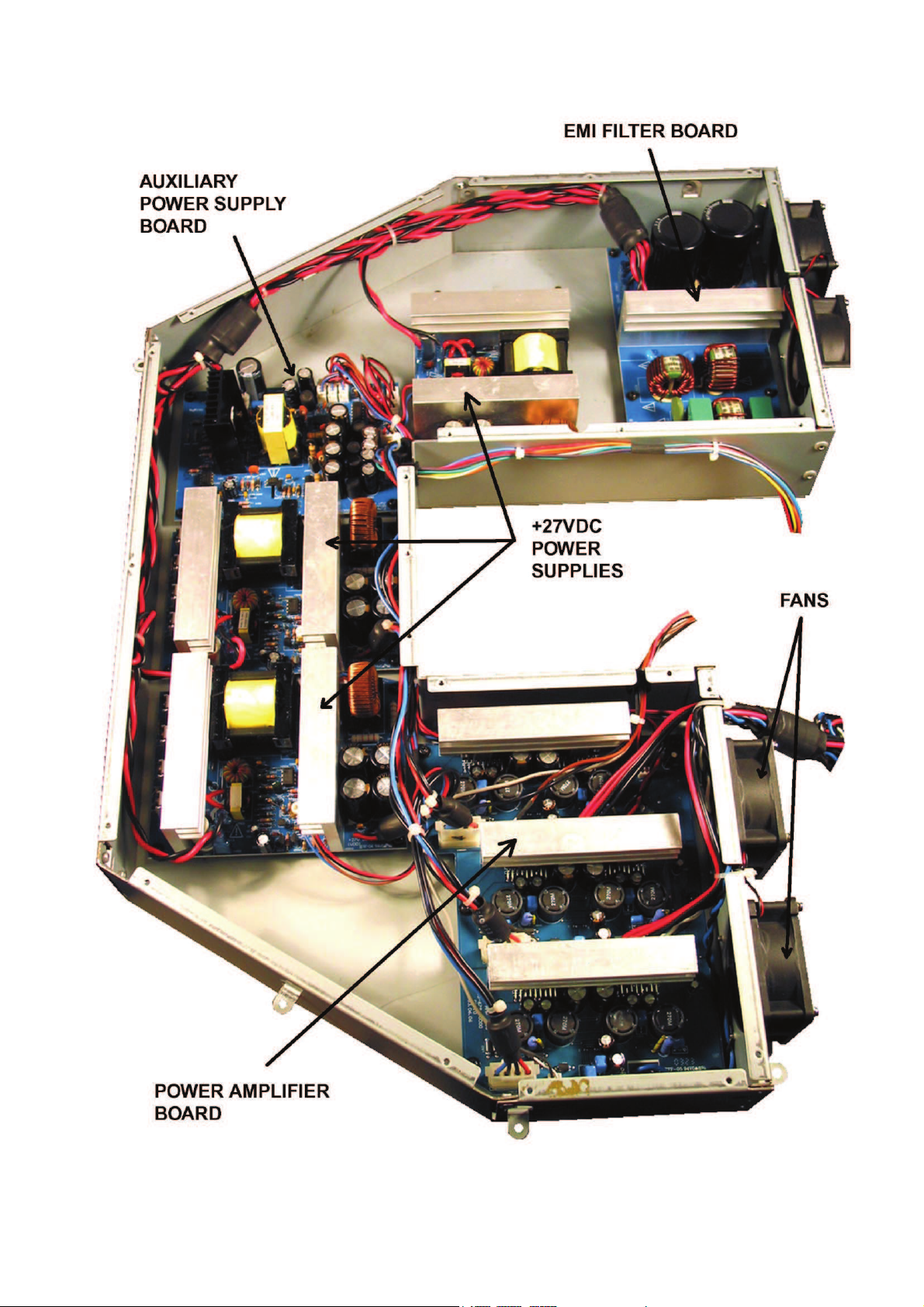
Figure 9. PS1 Power Stand Electronics Module with Top Cover Removed
Page 2

78
Power Stand Procedures
Note: Refer to Figure 9 for the following
procedures.
1. Lower Housing Removal
1.1 Place the power stand on a soft surface
so that the line array opening faces down.
1.2 Using a Phillips-head screwdriver,
remove the 19 screws that secure the lower
housing to the upper housing. Lift off the
lower housing.
2. Amplifier Housing Removal
2.1 Perform procedure 1.
2.2 Make a note of the wiring, and discon-
nect the wiring harnesses and connectors
that run to the amplifier housing. The amplifier housing is the large metal box with the
four fans.
2.3 Using a Phillips-head screwdriver,
remove the four screws that secure the
power stand base plate to the bottom of the
line array cavity. Lift it off of the cavity. Be
careful not to damage any wires.
2.4 Once all of the wiring is disconnected,
use a Phillips-head screwdriver to remove
the 16 screws that secure the amplifier
housing to the power stand upper housing.
Carefully lift the amplifier housing out of the
power stand upper housing.
3. Line Array Cavity Removal
3.1 Perform procedure 2.
3.2 Using a Phillips-head screwdriver,
remove the three screws that secure the line
array cavity to the upper housing. Lift the line
array cavity off of the upper housing. The
power stand foot pedal will disengage from
the shaft.
Disassembly Procedures
Page 3

79
4. Amplifier PCB Removal
4.1 Perform procedure 2.
4.2 Make a note of the wiring and disconnect
all of the wiring harnesses that connect the
power supply box to the DSP PCB and to the
microprocessor PCB.
4.3 Using a Phillips-head screwdriver,
remove the 24 screws that secure the power
supply box top cover in place. Lift off the top
cover.
4.4 Once you have the top cover off, make a
note of the wiring configuration and unplug
the wiring harnesses that connect to the
amplifier PCB.
4.5 Using a Phillips-head screwdriver,
remove the 6 screws that secure amplifier
PCB in place. Lift the amplifier PCB out of
the chassis.
5. Switching DC Power Supply Removal
5.1 Perform procedure 2.
5.2 Make a note of the wiring and disconnect
all of the wiring harnesses that connect the
power supply box to the DSP PCB and to the
microprocessor PCB.
5.3 Using a Phillips-head screwdriver,
remove the 24 screws that secure the power
supply box top cover in place. Lift off the top
cover.
5.4 Once you have the top cover off, make a
note of the wiring configuration and unplug
the wiring harnesses that connect to the
switching DC power supply PCB you wish to
remove.
5.5 Using a Phillips-head screwdriver,
remove the 4 screws that secure power
supply PCB in place. Lift the power supply
PCB out of the chassis.
Disassembly Procedures
Page 4
80
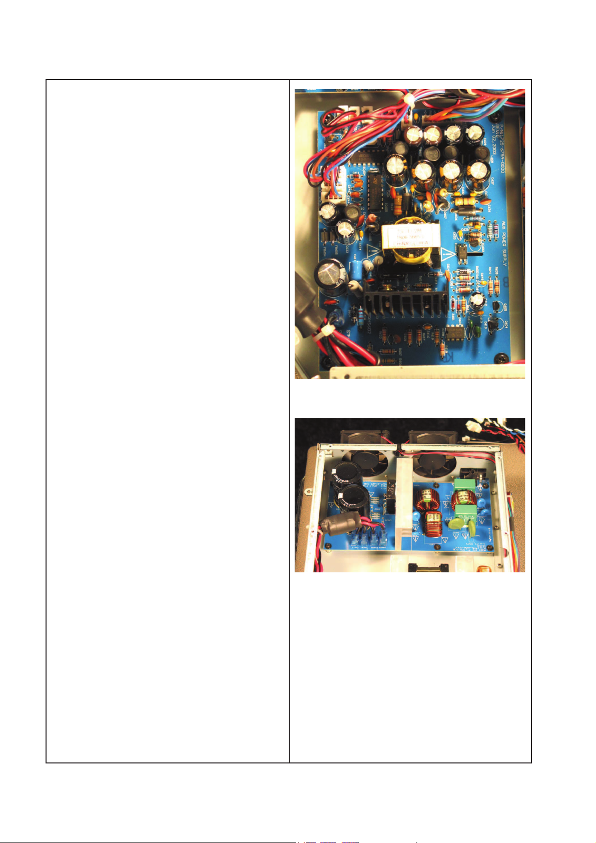
6. Auxiliary Power Supply Removal
6.1 Perform procedure 2.
6.2 Make a note of the wiring and disconnect
all of the wiring harnesses that connect the
power supply box to the DSP PCB and to the
microprocessor PCB.
6.3 Using a Phillips-head screwdriver,
remove the 24 screws that secure the power
supply box top cover in place. Lift off the top
cover.
6.4 Once you have the top cover off, make a
note of the wiring configuration and unplug
the wiring harnesses that connect to the
switching DC power supply PCB you wish to
remove.
6.5 Using a Phillips-head screwdriver,
remove the 4 screws that secure power
supply PCB in place. Lift the power supply
PCB out of the chassis.
7. EMI Filter PCB Removal
7.1 Perform procedure 2.
7.2 Make a note of the wiring and disconnect
all of the wiring harnesses that connect the
power supply box to the DSP PCB and to the
microprocessor PCB.
7.3 Using a Phillips-head screwdriver,
remove the 24 screws that secure the power
supply box top cover in place. Lift off the top
cover.
7.4 Once you have the top cover off, make a
note of the wiring configuration and unplug
the wiring harnesses that connect to the EMI
Filter PCB.
7.5 Using a Phillips-head screwdriver,
remove the 4 screws that secure the EMI
Filter PCB in place. Lift the EMI Filter PCB
out of the chassis.
Disassembly Procedures
Page 5

81
8. Chassis Fan Removal
8.1 Perform procedure 2.
8.2 Using a Phillips-head screwdriver,
remove the 24 screws that secure the power
supply box top cover in place. Lift off the top
cover.
8.3 Using a Phillips-head screwdriver,
remove the 4 screws that secure the fan to
the chassis.
8.4 Follow the wire harness for the fan you
are removing to the auxiliary power supply
PCB and unplug it. Lift the fan out of the
chassis.
Re-assembly note: When installing the new
fan, be sure to match the orientation of the
fan next to it so that it will move air in the
proper direction when in use.
9. Microprocessor PCB Removal
9.1 Perform procedure 1.
9.2 Make a note of the wiring configuration
and unplug the six wire harnesses from the
connectors on the board.
9.3 Lift the microprocessor PCB off of the
connectors that engage it on the bottom of
the board and the pins that connect to the
preset switches.
Re-assembly note: When re-installing this
PCB, be sure that all of the pins from the
preset switches are straight and properly
engage the connectors on the bottom of the
microprocessor PCB.
Disassembly Procedures
Page 6

82
Disassembly Procedures
10. DSP PCB Removal
10.1 Perform procedure 1.
10.2 Make a note of the wiring configuration
and unplug the six wire harnesses from the
connectors on the board.
10.3 Using a pair of needle-nose pliers,
compress the bottoms of the plastic standoff
posts used to attach the DSP PCB to the
Input/Output PCB. Lift the DSP PCB off of
the I/O PCB.
11. Input/Output PCB Removal
11.1 Perform procedures 9 and 10.
11.2 On the front panel of the power stand,
remove the four knobs for the mic trim and
level controls.
11.3 Using a nut driver, remove the nine nuts
and washers for the 1/4 inch phono jacks.
11.4 Using a Phillips-head screwdriver,
remove the 16 screws that secure the XLR,
Data in/out and Neutrik connectors to the
front panel.
11.5 Lift the I/O PCB off of the input panel.
Page 7

83
Disassembly Procedures
Line Array Procedures
Note: The line arrays are divided into a
lower line array, which plugs directly into the
power stand, and an upper line array, which
uses a bayonet arrangement to align the
upper array to the lower array for connection. All electrical connections are automatically made when the arrays are mounted
into the power stand and the upper array is
mounted to the lower array.
Note: Refer to Figure 7 for the following
procedures.
1. Grille Removal
1.1 Using a Phillips-head screwdriver,
remove the six screws that secure the end
cap to the line array enclosure. Lift off the
end cap. Unplug the molex connector from
the speaker harness.
1.2 Grasp the edge of the grille and gently
lift it away from the enclosure.
2. Nameplate Removal
2.1 Perform procedure 1.
2.2 On the back of the grille, unbend the
legs of the logo. Lift off the nameplate.
3. Driver Removal
3.1 Perform procedure 1.
3.2 Using a Phillips-head screwdriver,
remove the four screws that secure the
driver to the enclosure.
3.3 Lift the driver out of the enclosure. Note
the wiring configuration and cut the wires as
close to the driver terminals as possible.
4. Upper Line Array Top End Cap Removal
4.1 Using a Phillips-head screwdriver,
remove the seven screws that secure the
end cap to the line array enclosure. Lift off
the end cap.
Re-assembly note: Make sure that the end
cap gasket is properly aligned to achieve an
airtight seal.
5. Upper Line Array Bottom End Cap
Removal
5.1 Using a Phillips-head screwdriver,
remove the seven screws that secure the
end cap to the line array enclosure. Lift the
end cap away from the enclosure. Unplug
the molex connector from the speaker
harness.
Re-assembly note: Make sure that the end
cap gasket is properly aligned to achieve an
airtight seal.
6. Lower Line Array Top End Cap Removal
6.1 Using a Phillips-head screwdriver,
remove the six screws that secure the end
cap to the line array enclosure. Lift off the
end cap. Unplug the molex connector from
the speaker harness.
Re-assembly note: Make sure that the end
cap gasket is properly aligned to achieve an
airtight seal.
7. Lower Line Array Bottom End Cap
Removal
7.1 Using a Phillips-head screwdriver,
remove the seven screws that secure the
end cap to the line array enclosure. Lift the
end cap away from the enclosure. Unplug
the molex connector from the speaker
harness.
Re-assembly note: Make sure that the end
cap gasket is properly aligned to achieve an
airtight seal.
Page 8

84
Disassembly Procedures
8. Front Cap Removal
8.1 Using a Phillips-head screwdriver,
remove the four screws that secure the front
cap to the bottom front of the line array
enclosure. Lift the end cap away from the
enclosure.
Bass Module Procedures
Note: Refer to Figure 8 for the following
procedures.
1. Grille Removal
1.1 Using an allen wrench, remove
the four screws that secure the grille to the
upper and lower speaker end caps.
1.2 Lift off the grille.
2. Nameplate Removal
2.1 Perform procedure 1.
2.2 On the back of the grille, remove the
retaining nut and spring from the post of the
nameplate. Lift the nameplate off of the
grille.
3. Driver Removal
3.1 Perform procedure 1.
3.2 Using a Phillips-head screwdriver,
remove the four screws that secure the
driver to the bass module enclosure.
3.3 Lift the driver out of the enclosure. Note
the wiring configuration and cut the wires as
close to the driver terminals as possible.
Re-assembly notes:
- When soldering the speaker harness wires
to the new driver, be sure to observe polarity
of the driver harness wires.
- Be sure to properly align the gasket behind
the new driver to ensure an airtight fit.
4. Input Panel Removal
4.1 Using a Phillips-head screwdriver,
remove the four screws that secure the
input panel to the bass module enclosure.
4.2 Lift the input panel away from the bass
module enclosure.
4.3 Make a note of the wiring configuration
and un-solder the speaker harness wires
from the input panel.
Page 9
85
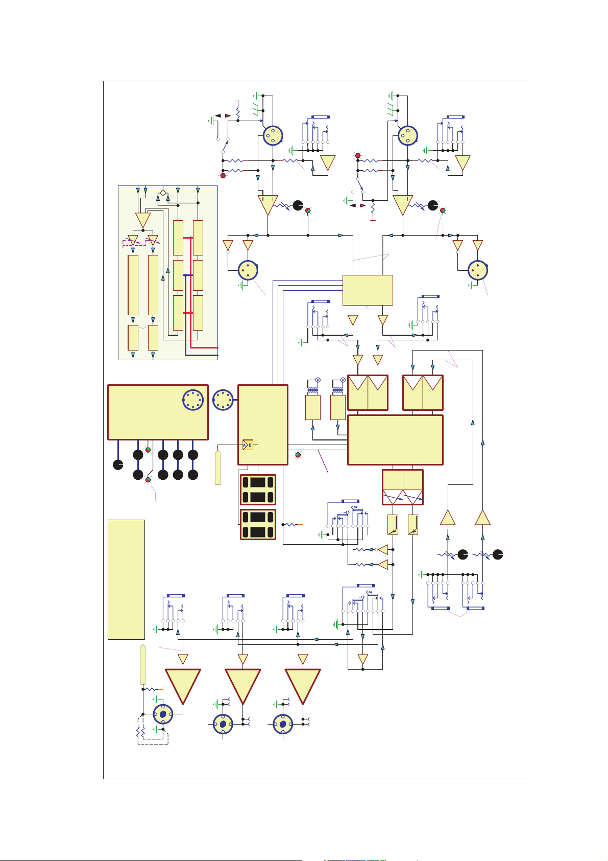
Figure 10. PS1 Power Stand Block Diagram
BLOCK DIAGRAM - Signal Processing + Routing
U
Rev:
0 1
Input-LINE
1 2
3
Input-MIC
INA163
+8 to +50 dB
Trim
PHANTOM
+24
Off
+24v
A/D
CS5361
D/A
CS4392
PHANTOM
Ch1
Digital
Volume
Control
2-Ch.
A/D
Ch1 Insert
Ch2 Insert
High
Remote
Level
Mid
Low
Ch1 Ch2
Ring = Send
Tip = Return
µC
5
432
1
678
9
All-Amps
D/A
12
3
Ch1 Line Out
12
3
Ch2 Line Out
Master
Amp In 1
Amp In 3
Amp In 2
Power
Amp
Amp1
Power
Amp
Amp2
Power
Amp
Amp3
Hi/Full Range
Bass
Bass
LineSource Top
Master Vol Ctrl
0 1
PRESET
Ch1 Ch2
8/4 ohm Sense
8/4 ohm Sense
1-
2+
2-
1+
+5
1-
2+
2-
1+
1-
2+
2-
1+
LineSource Bottom
Sig/OL
Sig/OLSig/OL
BASS SPEAKER SENSING:
R=Open: Amp1&2 Wider-Band EQ
R=10K: 40-150Hz X-Over on Bass, >150Hz-Hi
R=5K: X-Over on Bass Ch, -6dB Hi Range
R<5K: Debug Mode: All outs flat, Limiter Off
Data In
Data-Out
SPDIF
Rcvr
Ring = Send
Tip = Return
DSP
CS8416
A/D
CS5361
+20dB
A/D
Ch 3 IN
Ch 4 IN
20K 15A
Level
Level
+20dB
20K 15A
DSP Processing Block Diag
-1
+1
Ch1/2 Preset
Remote
Ch1 In
Ch2 In
Ch 3 In
Ch 4 In
Hi Out
Bass Out
Sys. EQ+X-Over, Hi
L
R
S-DATA Out
Limiter
S3PC8475
TCA9459F
User EQ Preset EQNoiseGate
User EQ Preset EQNoiseGate
(to SPDIF)
(SPDIF)
(SPDIF)
ADS21065L
+1dBV (1.1V) for
250W@4 Ohms
+29dB
+29dB
+29dB
Clip @ +30dBV
Master Vol. Range: -80 to +22dB (+10 @ 12:00)
Sys. EQ+X-Over, Lo Limiter
(250W 4ohms)
5K 10C
Nom.: 0dBV
Clip@+18dBV
Max. Gain = 0dB
Nom. Gain = -10dB (12:00)
Min. Gain = -40dB
Red=Clip=+6dBV
Green=Signal= -30dBV
Knee=+1.5dBV
Clip= -4dBV into A/D
Signal= -40dBV into A/D
Max. Level = +40dBV+
Nom. Level = -13dBV (pot @ ctr)
Min. Level = -30dBV for full output
Nom. -10dBV
Clip@+6dBV
Nom. -10dBV
Clip@+6dBV
Nom. -10dBV
Clip@+6dBV
Max. Level = +18dBV [input buffer clips]
Nom. Level = -1dBV
Min. Level = -46dBV for full output
(Ch1 Vol+Master @ Max)
Max. Level = +10dBV
Nom. Level = -21dBV(Trim ctr)
Min. Level = -66dBV for full output
(Trim, Ch1 Vol+Master @ Max)
+21dB @ ctr
Persistence = 100msec
0dB
0dB
Nom.: +6dBV (Balanced)
Clip@+24dBV "
0dB
0dB
0dB
0dB
0dB
-1.5dB
-1.5dB
Nom.: +6dBV (Balanced)
Clip@+24dBV "
5
432
1
678
9
Bass Send
Input
+5
Bass Slave Sense
SPDIF
Xmiter
CS8406
Power / Protect / Diagnostic
0dB
-1 +1
+1
+1
+1
+1
+1
+1
LPF
LPF
+1
+1
+1
-1
+1
-20dB
Mic (XLR) input
-12 to +30 dB
+1dB @ ctr
Line (1/4") input
Input-LINE
1 2
3
Input-MIC
INA163
+8 to +50 dB
Trim
Ch2
Sig/OL
5K 10C
+21dB @ ctr
+1
-20dB
Mic (XLR) input
-12 to +30 dB
+1dB @ ctr
Line (1/4") input
+24
Off
+24v
+2.6dB @ 12:00
Page 10

86
Test Procedures
PS1 Power Stand Tests
Equipment Required
• dB Meter
• Digital Multi-meter
• Audio Signal Generator
• Distortion Meter
• 3 - 4 Ohm, 250 Watt Load Resistors
• Test cables, see Appendix
Overall PS1 System Tests
Notes:
1. Do not connect the R1 remote control for
the following tests, unless specified. Powering up the PS1 power stand without the
remote has the same effect as setting all of
the controls on the remote to the midpoint.
2. On the front panel of the PS1, set the
Channel 1 and Channel 2 Preset Select
switches to 00. Short out the 2+ and 2connections on the Amp 3 out connector
using the test cable described in section 1 of
the appendix of this manual. This will put the
PS1 into debug mode for the following tests.
In this mode the crossover, the compressor
and the EQ are disabled. The DSP will pass
a flat response. The level controls and the
clip indicators still operate in this mode.
3. Refer to Figure 10, PS1 Block Diagram,
for the following procedures.
1. Channel 1 and 2 Mic Input Gain Tests
1.1 Place a 1/4! mono shorting plug into the
Amp 2 IN and Amp 3 IN jacks on the right
hand side of the input/output panel. This will
disable the channel 2 and 3 amplifiers while
testing the channel 1 amplifier.
1.2 On the left hand side of the input/output
panel, set the channel 1 Mic Trim control to
the 6 setting. Ensure that the Phantom
Power push button is not pushed in.
1.3 Using a balanced XLR male input cable,
apply a 1 kHz, -30dBV signal to the channel
1 input.
1.4 Reference a dB meter to the input level.
Measure the gain output at the Amp 1 OUT
jack. It should be +48.5 dB
+ 3 dB.
1.5 Move the shorting plug from the Amp 2
IN jack to the Amp 1 IN jack and repeat
steps 1.1 to 1.4 for the channel 2 Mic input.
2. Channel 1 and 2 Mic Input Frequency
Reponse and Distortion Tests
2.1 Place a 1/4! mono shorting plug into the
Amp 2 IN and Amp 3 IN jacks on the right
hand side of the input/output panel. This will
disable the channel 2 and 3 amplifiers while
testing the channel 1 amplifier.
2.2 On the left hand side of the input/output
panel, set the channel 1 Mic Trim control to
the 6 setting. Ensure that the Phantom
Power push button is not pushed in.
2.3 Using a balanced XLR male input cable,
apply a 1 kHz, -30 dBV signal to the channel
1 input.
2.4 Use an 80kHz low-pass filter on your
measuring equipment. Reference a dB
meter to the input level. Measure the frequency response at the Amp 1 OUT jack. It
should be 0 dB
+ 3 dB from 30 Hz to 15 kHz.
2.5 Measure the Total Harmonic Distortion
(THD) level at the Amp 1 OUT jack.
It should be 0.25% max at 1 kHz and 1.5%
max at 15 kHz.
2.6 Move the shorting plug from the Amp 2
IN jack to the Amp 1 IN jack and repeat
steps 2.1 to 2.5 for the channel 2 Mic input.
Page 11

87
Test Procedures
3. Channel 1 and 2 Mic Input Signal to
Noise Ratio (Dynamic Range) Tests
3.1 Place a 1/4• mono shorting plug into the
Amp 2 IN and Amp 3 IN jacks on the right
hand side of the input/output panel. This will
disable the channel 2 and 3 amplifiers while
testing the channel 1 amplifier.
3.2 On the left hand side of the input/output
panel, set the channel 1 Mic Trim control to
the 6 setting. Ensure that the Phantom
Power push button is not pushed in.
3.3 Using a balanced XLR male input cable,
apply a 1 kHz, -30 dBV signal to the channel
1 input.
3.4 Reference a dB meter to the output level
at the Amp 1 OUT jack. Remove the input
signal and measure the A-Weighted output
level. It should be -80 dB minimum.
3.5 Move the shorting plug from the Amp 2
IN jack to the Amp 1 IN jack and repeat
steps 3.1 to 3.4 for the channel 2 Mic input.
4. Channel 1 and 2 Mic Input Phantom
Power Test
4.1 Plug an XLR connector into the channel
1 Mic input. Do not connect any cables to
the channel 1 or channel 2 Mic inputs.
Power on the unit.
4.2 Press the channel 1 phantom power
switch. Verify that the LED lights. Using a
DMM, measure the DC voltage level across
pins 1 and 2 of the XLR connector. Verify
that the DC level is +24Vdc
+ 1Vdc relative
to pin 1.
4.3 Measure the DC voltage level across
pins 1 and 3 of the XLR connector. Verify
that the DC level is +24Vdc + 1Vdc relative
to pin 1.
4.4 Repeat steps 4.1 to 4.3 for channel 2.
5. Channel 1 and 2 Line Input Gain Tests
5.1 Place a 1/4• mono shorting plug into the
Amp 2 IN and Amp 3 IN jacks on the right
hand side of the input/output panel. This will
disable the channel 2 and 3 amplifiers while
testing the channel 1 amplifier.
5.2 On the left hand side of the input/output
panel, set the channel 1 Mic Trim control to
the 6 setting. Ensure that the Phantom
Power push button is not pushed in.
5.3 Using an unbalanced 1/4• phono jack
input cable, apply a 1 kHz, -10 dBV signal
to the channel 1 input.
5.4 Reference a dB meter to the input level.
Measure the gain output at the Amp 1 OUT
jack. It should be +28.5 dB
+ 4 dB.
5.5 On the signal generator, turn the input
level all the way down. Verify that the channel 1 Signal/OL LED is off. Increase the
signal generator level. Verify that the LED
lights green. Increase the signal level again
and verify that the LED lights red.
Note: You may have to increase the Mic
Trim level on the PS1 channel 1 input as
well to get the LED to light red.
5.5 Move the shorting plug from the Amp 2
IN jack to the Amp 1 IN jack and repeat
steps 5.1 to 5.5 for the channel 2 Line input.
6. Channel 1 and 2 Line Input Frequency
Reponse and Distortion Tests
6.1 Place a 1/4• mono shorting plug into the
Amp 2 IN and Amp 3 IN jacks on the right
hand side of the input/output panel. This will
disable the channel 2 and 3 amplifiers while
testing the channel 1 amplifier.
6.2 On the left hand side of the input/output
panel, set the channel 1 Mic Trim control to
the 6 setting. Ensure that the Phantom
Power push button is not pushed in.
Page 12

88
6.3 Using an unbalanced 1/4! phono jack
input cable, apply a 1 kHz, -10 dBV signal
to the channel 1 input.
6.4 Use an 80 kHz low-pass filter on your
measuring equipment. Reference a dB
meter to the input level. Measure the frequency response at the Amp 1 OUT jack.
It should be 0 dB
+ 3 dB from 30 Hz to
15 kHz.
6.5 Measure the Total Harmonic Distortion
(THD) level at the Amp 1 OUT jack. It should
be 0.25% max at 1 kHz and 1.5% max at
15 kHz.
6.6 Move the shorting plug from the Amp 2
IN jack to the Amp 1 IN jack and repeat
steps 6.1 to 6.5 for the channel 2 Line input.
7. Channel 1 and 2 Line Input Signal to
Noise Ratio (Dynamic Range) Tests
7.1 Place a 1/4! mono shorting plug into the
Amp 2 IN and Amp 3 IN jacks on the right
hand side of the input/output panel. This will
disable the channel 2 and 3 amplifiers while
testing the channel 1 amplifier.
7.2 On the left hand side of the input/output
panel, set the channel 1 Mic Trim control to
the 6 setting. Ensure that the Phantom
Power push button is not pushed in.
7.3 Using an unbalanced 1/4! phono jack
input cable, apply a 1 kHz, -10 dBV signal to
the channel 1 input.
7.4 Reference a dB meter to the output level
at the Amp 1 OUT jack. Remove the input
signal and measure the A-Weighted output
level. It should be -80 dB minimum.
7.5 Move the shorting plug from the Amp 2
IN jack to the Amp 1 IN jack and repeat
steps 7.1 to 7.4 for the channel 2 Line input.
Test Procedures
8. Channel 3 and 4 Line Input Gain Tests
8.1 Place a 1/4! mono shorting plug into the
Amp 1 IN and Amp 2 IN jacks on the right
hand side of the input/output panel. This will
disable the channel 1 and 2 amplifiers while
testing the channel 3 amplifier.
8.2 On the left hand side of the input/output
panel, set the channel 3 Level control to the
6 setting.
8.3 Using an unbalanced 1/4! phono jack
input cable, apply a 1 kHz, -20 dBV signal to
the channel 1 input.
8.4 Reference a dB meter to the input level.
Measure the gain output at the Bass/Amp 3
OUT jack. It should be +40.1 dB
+ 3 dB.
8.5 Repeat steps 8.1 to 8.4 for the channel
4 Line input.
9. Channel 3 and 4 Line Input Frequency
Reponse and Distortion Tests
9.1 Place a 1/4! mono shorting plug into the
Amp 1 IN and Amp 2 IN jacks on the right
hand side of the input/output panel. This will
disable the channel 1 and 2 amplifiers while
testing the channel 3 amplifier.
9.2 On the left hand side of the input/output
panel, set the channel 4 Mic Trim control to
the 6 setting.
9.3 Using an unbalanced 1/4! phono jack
input cable, apply a 1 kHz, -20 dBV signal
to the channel 1 input.
9.4 Use an 80 kHz low-pass filter on your
measuring equipment. Reference a dB
meter to the input level. Measure the frequency response at the Amp 1 OUT jack.
It should be 0 dB + 3 dB from 30 Hz to
15 kHz.
9.5 Measure the Total Harmonic Distortion
(THD) level at the Amp 1 OUT jack. It should
be 0.25% max at 1 kHz and 1.5% max at
15 kHz.
Page 13

89
9.6 Repeat steps 9.1 to 9.5 for the channel
4 Line input.
10. Channel 3 and 4 Line Input Signal to
Noise Ratio (Dynamic Range) Tests
10.1 Place a 1/4! mono shorting plug into
the Amp 1 IN and Amp 2 IN jacks on the
right hand side of the input/output panel.
This will disable the channel 1 and 2 amplifiers while testing the channel 3 amplifier.
10.2 On the left hand side of the input/
output panel, set the channel 3 Level
control to the 6 setting.
10.3 Using an unbalanced 1/4! phono jack
input cable, apply a 1 kHz, -10 dBV signal to
the channel 1 input.
10.4 Reference a dB meter to the output
level at the Bass/Amp 3 OUT jack. Remove
the input signal and measure the AWeighted output level. It should be -80 dB
minimum.
10.5 Repeat steps 10.1 to 10.4 for the
channel 4 Line input.
11. Channel 1 and 2 Remote Control,
Preset Switch and Insert Function Tests
11.1 Connect the PS1 power stand to a
known good L1 line array. Set the channel 1
preset switch to 00. Connect the remote
control to the unit using the remote control
MIDI cable supplied with the PS1.
11.2 Connect an analog audio source to the
Channel 1 line input 1/4 inch jack. This
source can be a CD player with a music
disc.
11.3 Adjust the trim level so that the LED is
lit mostly green. The audio should sound
normal.
Test Procedures
11.4 With the audio playing, change the
channel 1 preset to 97 and back to 00. The
channel should mute gracefully when the
preset switch is operated. The audio should
fade back in again about a second after the
switch has stopped operating.
Note: Preset 97 is a 1 kHz band pass
(telephone-type sound). Preset 00 should
sound normal.
11.5 Operate all channel 1 controls on the
remote (high, mid, low, volume and master
volume). All tone controls should have a
clearly audible effect and operate smoothly.
Channel volume may display a little "zipper!
noise, which is normal.
Note: Channel volume all the way down
does not mute the channel, but the output
level should be very low. There is a small,
but noticeable time delay between operating
the control and the audible effect. This is
normal. The master volume control should
operate smoothly without any artifacts.
11.6 Insert a 1/4 inch phono jack all the way
into the channel 1 Insert jack. The audio
should sound normal.
11.7 Insert a 1/4 inch phono jack into the
channel 3 Line IN jack and operate the
volume control on the power stand. The
audio should sound normal.
11.8 Repeat steps 11.1 to 11.7 for the channel 2 input.
12. Channel 1 Send, Line Output and
Digital Output Tests
Note: For these tests you will need an
external device that can accept both 1/4
inch and XLR inputs. A small mixer, such
as a Mackie or Behringer with headphones
connected works well for this. The master
volume control on the PS1#s remote control
should be set all the way down to mute all
sound coming from the unit under test.
Page 14

90
Test Procedures
12.1 Connect the PS1 power stand to a
known good L1 line array. Set the channel 1
preset switch to 00. Connect the remote
control to the unit using the remote control
MIDI cable supplied with the PS1.
12.2 Connect an analog audio source to the
Channel 1 Line IN 1/4 inch jack. This source
can be a CD player with a music disc.
12.3 Adjust the trim level so that the LED is
lit mostly green. The audio should sound
normal.
12.4 Insert a 1/4 inch plug halfway into the
channel 1 Insert jack. The audio should
sound normal.
12.5 Connect the PS1 channel 1 XLR Line
OUT jack to the XLR input of the mixer. The
audio should sound normal.
Note: The PS1 puts out a “professional”
+4dBu level. You may have to turn the the
input trim control on the mixer all the way
down to prevent overloading the signal and
distorting it.
12.6 Connect the Data Out jack of the PS1
to a device that accepts a 48 kHz S/PDIF
data stream. The audio should sound normal.
13. Power Amplifier Tests
13.1 Connect the PS1 power stand to a
known good L1 line array. Set the channel 1
preset switch to 00. Connect the remote
control to the unit using the remote control
MIDI cable supplied with the PS1.
13.2 Connect an analog audio source to the
Amp 1 IN 1/4 inch phono jack. This source
can be a CD player with a music disc.
13.3 Verify that the audio comes from the
upper section of the L1 line array. The audio
should sound clean and undistorted.
13.4 Connect the audio source to the Amp 2
IN 1/4 inch phono jack. Verify that the audio
comes from the lower section of the L1 line
array. The audio should sound clean and
undistorted.
13.5 Connect a B1 bass module to the PS1
power stand at the Bass/Amp 3 OUT jack.
Connect the audio source to the Amp 3 IN
1/4 inch phono jack. Sound should come
from the bass module only and be clean and
undistorted.
13.6 Connect the audio source to the All
Amps IN 1/4 inch phono jack. Sound should
come from both of the L1 line array sections
and the bass module simultaneously. The
audio should be clear and undistorted.
14. High SPL System Sweep Test
CAUTION: This test will be extremely loud.
Hearing protection is advised.
14.1 Connect a R1 remote control to the
PS1 power stand under test. Set the channel 1 controls to mid-level. Set the master
volume control on the remote to the 1
o’clock position. Set the channel 1 Mic Trim
control on the PS1 to 6. Connect a L1 line
array to the PS1. Connect a B1 bass module to the PS1.
14.2 Connect a signal generator to the
channel 1 input on the PS1. Adjust the
signal generator and/or trim control so that
the Signal/OL LED is just below red.
14.3 Sweep the input frequency from 40 Hz
to 14 kHz. Listen for any unusual noises and
excessive distortion or drop-outs.
15. Bass Module Auto-EQ Test
15.1 Connect a L1 line array to the PS1
power stand. Connect an R1 remote control
to the power stand. Connect a B1 bass
module to the Bass/Amp 3 OUT jack on the
power stand. Connect an audio source to
the channel 1 and 2 inputs of the power
stand.
Page 15

91
Test Procedures
15.2 Set the channel 1 and 2 level controls
to identical settings so that both LEDs are
mainly green.
15.3 While the audio is playing, disconnect
the B1 bass module from the power stand.
The system should mute and un-mute and
audio should resume. The audio should
sound normal, but not punchy (no deep
bass).
15.4 Plug a dummy 1/4 inch phono jack into
the Bass Line Out jack. The system should
mute and un-mute again, but the audio
should sound thinner than before.
15.5 Remove the dummy plug. The system
should mute and un-mute and the audio
should sound normal again.
15.6 Re-connect the B1 bass module to the
power stand. The audio should mute and unmute again and sound normal.
15.7 Connect a second B1 bass module to
the first one. The audio should mute and unmute. The audio will sound very similar to
having only one bass module attached.
Disconnect the second bass module. The
system should mute and un-mute and the
audio should sound normal again.
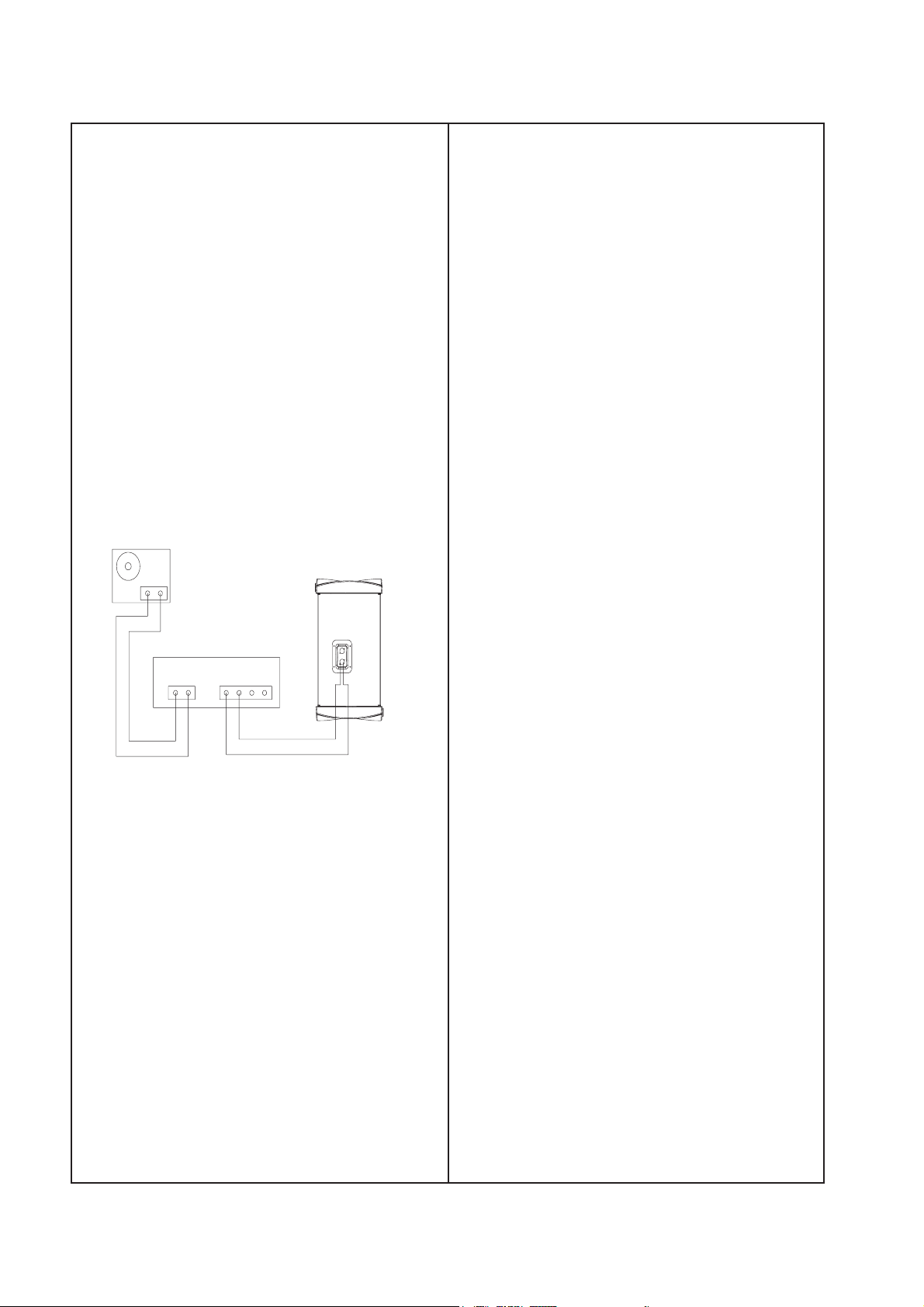
L1 Line Array Tests
Set up the unit under test as shown below.
1. Air Leak Test
1.1 Apply a 100 Hz, 10 Vrms sine wave to
the unit under test.
1.2 Listen carefully for air leaks from around
the end cap, the transducers and the grille.
Air leaks will be heard as a hissing or sputtering sound. All repairs must be hidden.
Test duration should be 5 seconds minimum.
2. Transducer Rub and Tick Test
2.1 Remove the transducer you wish to test
using the disassembly procedures in this
manual. Do not unplug the wires at the
transducer assembly terminals.
2.2 Connect a signal generator directly to
the terminals of the transducer assembly
under test.
2.3 Apply a 20 Hz, 5 Vrms signal to the
transducer assembly.
2.4 Listen carefully for any extraneous
noises such as rubbing, scraping or ticking.
Note: To distinguish between normal suspension noise and rubs or ticks, displace the
cone slightly with your fingers. If the noise
stays the same, it is normal suspension
noise and the driver is good. Suspension
noise will not be heard with program material.
3. Transducer Phase Test
3.1 Apply a DC voltage of 10V, positive
applied to the positive tab of the dual
banana jack on the line array test cable and
negative applied to negative (gnd) tab.
3.2 All of the driver cones should move
outward when the DC voltage is applied.
3.3 Rewire any incorrectly connected transducers.
Power Amplifier
INPUT OUTPUT
Audio Signal
Generator
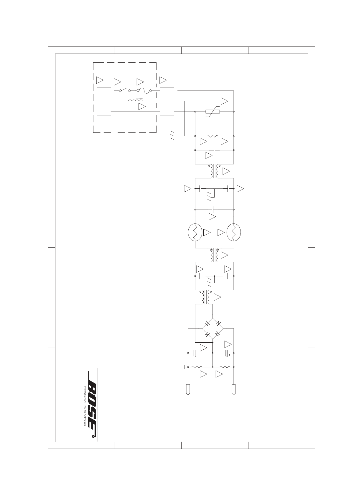
Upper or Lower
L1 Line Array
Upper or Lower L1
Line Array Test Cable
Page 16
92
Test Procedures
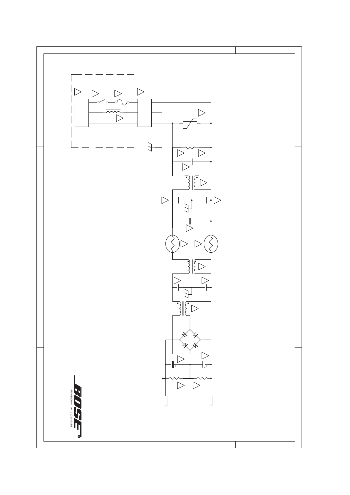
Power Amplifier
INPUT OUTPUT
Audio Signal
Generator
B1 Bass Module
Test Cable
B1 Bass Module
4. L1 Line Array Sweep Test
4.1 Set up the upper or lower line array
section as shown in the figure on the previous page.
4.2 Apply a 100 Hz, 10 Vrms sine wave to
the input.
4.3 While listening to the output of the
system, sweep the input frequency slowly
from 100 Hz to 15 kHz.
4.4 Listen carefully for any extraneous
noises such as buzzing and ticking.
B1 Bass Module Tests
Set up the unit under test as shown below.
1. Air Leak Test
1.1 Apply a 100 Hz, 20 Vrms sine wave to
the unit under test.
1.2 Listen carefully for air leaks from around
the end cap, the transducers and the grille.
Air leaks will be heard as a hissing or sputtering sound. All repairs must be hidden.
Test duration should be 5 seconds minimum.
2. Transducer Rub and Tick Test
2.1 Remove the transducer you wish to test
using the disassembly procedures in this
manual. Do not unplug the wires at the
transducer assembly terminals.
2.2 Connect a signal generator directly to
the terminals of the transducer assembly
under test.
2.3 Apply a 10 Hz, 10 Vrms signal to the
transducer assembly.
2.4 Listen carefully for any extraneous
noises such as rubbing, scraping or ticking.
Note: To distinguish between normal suspension noise and rubs or ticks, displace the
cone slightly with your fingers. If the noise
stays the same, it is normal suspension
noise and the driver is good. Suspension
noise will not be heard with program material.
3. Transducer Phase Test
3.1 Apply a DC voltage of 20V, positive
applied to the positive tab of the dual
banana jack on the bass module test cable
and negative applied to negative (gnd) tab.
3.2 Notice carefully that all driver cones
should move outward when the DC voltage
is applied.
3.3 Rewire any incorrectly connected transducers.
4. System Sweep Test
4.1 Set up the system as shown in the
figure at left.
4.2 Apply a 10 Hz, 20 Vrms sine wave to the
input.
4.3 While listening to the output of the
system, sweep the input frequency slowly
from 10 Hz to 400 Hz.
4.4 Listen carefully for any extraneous
noises such as buzzing and ticking.
Page 17
93
1 2
A
B
C
D
4
321
D
C
B
A
4
3
L603
3.8mH
L604
1mH
C601
1uF 300V
C602
1uF 300V
C604
1n5
C603
1n5
R601
220K 3W
DB601
MB354S
R603
100K 1/2W
R604
100K 1/2W
ACGND
F601
15A 125VAC
C607
2200uF 200V
C608
2200uF 200V
SW601
20A 125V
C606
1n5
C605
1n5
N
E
L
CN601
IEC
1 2
TH601
SCK2R515
V+
EGND
( Earth GND)
1 2
TH602
SCK2R515
(16A)
(16A)
L602
3.8mH
(16A)
VDR601
14D271K
!
!
!
!
!
!
!
!
!
!
!
!
!
!
!
!
!
!
!
!
L601
N
E
L
CN602
DT-4-3P
!
!
(CN603,605,607,609)
(CN604,606,608,610)
ACGND
(TO AUX PS AND +/-27V PS)
(TO AUX PS AND +/-27V PS)
!
70uH 6Ts
PS1 Power Stand
FCC Filter PCB, Rev. F
P/N:
275436
Sheet 1 of 1
120V Version 1.0 Systems
Page 18
94
1 2 3 4
A
B
C
D
4
321
D
C
B
A
L603
3.8mH
L604
1mH
C601
1uF 300V
C602
1uF 300V
C604
1nF
C603
1nF
R601
220K 3W
DB601
GL3506
R603
100K 1/2W
R604
100K 1/2W
ACGND
F601
10A 250VAC
C607
2200uF 200V
C608
2200uF 200V
SW601
15A 250V
C606
1nF
C605
1nF
N
E
L
CN601
IEC
1
2
TH601
SCK0512
V+
EGND
( Earth GND)
1
2
TH602
SCK0512
(16A)
(16A)
L602
3.8mH
(16A)
VDR601
14D471K
!
!
!
!
!
!
!
!
!
!
!
!
!
!
!
!
!
!
!
!
L601
N
E
L
CN602
DT-4-3P
!
!
(CN603,605,607,609)
(CN604,606,608,610)
ACGND
(TO AUX PS AND +/-27V PS)
(TO AUX PS AND +/-27V PS)
!
70uH,6Ts
PS1 Power Stand
FCC Filter PCB, Rev. F
P/N: 283370
Sheet 1 of 1
120V Version 1.1 Systems
Page 19

95
1 2 3 4
A
B
C
D
4
321
D
C
B
A
L603
3.8mH
L604
1mH
C601
1uF 300V
C602
1uF 300V
C604
1nF
C603
1nF
R601
220K 3W
DB601
GL3506
R603
100K 1/2W
R604
100K 1/2W
ACGND
F601
10A 250VAC
C607
2200uF 200V
C608
2200uF 200V
SW601
15A 250V
C606
1nF
C605
1nF
N
E
L
CN601
IEC
1
2
TH601
SCK0512
V+
EGND
( Earth GND)
1
2
TH602
SCK0512
(16A)
(16A)
L602
3.8mH
(16A)
VDR601
14D471K
!
!
!
!
!
!
!
!
!
!
!
!
!
!
!
!
!
!
!
!
L601
N
E
L
CN602
DT-4-3P
!
!
(CN603,605,607,609)
(CN604,606,608,610)
ACGND
(TO AUX PS AND +/-27V PS)
(TO AUX PS AND +/-27V PS)
!
70uH,6Ts
PS1 Power Stand
FCC Filter PCB, Rev. F
P/N: 283369
Sheet 1 of 1
230V Version 1.0 and 1.1 Systems
Page 20

96
1 2 3 4 5 6 7
A
B
C
D
8
7654321
D
C
B
A
8
Z501
18V
Z502
18V
R501
1K
R507
51R
Q501
IRF840
R508
51R
Q502
IRF840
D501
UF4006
Q503
IRF840
Q504
IRF840
R509
51R
R510
51R
R502
1K
Z503
18V
Z504
18V
D502
UF4006
R511
100/2W
C501
100p 1KV
R512
47R 2W
C502
1nF
C503
1nF
R513
47R 2W
D503
BYV32-200
C504
2200uF 35V
C505
2200uF 35V
D504
BYV32-200
C523
100n
D510
1N4148
R514
560R
C515
123
R515
470R
C517
222
R503
8.2K
D511
1N4148
C518
102
D505
1N4148
R516
47K
D506
1N4148
R517
33R
Q505
2N3904
Q507
2N3906
R518
750R 1W
C519
1uF/50V
C508
100n
C516
103
R519
240R
R520
39R
D509
UF4003
ACGND
C520
100uF/50V
C510
100n
D507
1N4148
R521
39K
R522
3K
Q506
2N3904
R523
12K
R524
47K
Z505
18V
R525
200K
R504
1K
TP501
1KB
R505
1K
D508
1N4148
R526
12K
T501
TT-9972
1
4
5
6
7
8
EGND
DGND
C506
2200uF 35V
C522
2200uF 35V
C511
100n
C512
100n
T502
TT-9971
3
1
5
6
3
7
9.10
11.12
13.14
15.16
T503
ETD39
COMP
1
VFB
2
ISEN
3
RT/CT
4
GND
5
OUT
6
VCC
7
VREF
8
IC501
UC2842B
FB501
FB502 FB504
FB503
FB505
FB506
R506
12K
R527
12K
C513
1nF
ACGND
L501
200uH
D512
1N4148
V+
(-27V)
(+27V)
+24VD
VDD
VSS
( Earth GND)
( Digital GND)
FB507
FB508
R528
47R 2W
R529
47R 2W
C524
1nF
C525
1nF
FB509
FB510
FB511
FB512
(or SYN2,SYN3)
FB513
ACGND
NOTE:
This schematic can be applied to three +/-27V power supplies
FAULT
SYN1
12
TH501
BD222/100C
R530
22K
Q508
2N3906
C514
100n
C507
22uF 400V
!
!
!
(FROM EMI FILTER )
(FROM AUX PS CN615 or CN616,CN617)
(TO D AMP CN802A or CN806A,CN810A)
ACGND
(CN501)
(CN502)
(FROM EMI FILTER)
123
4
CN503
(TO D AMP CN802A or CN806A,CN810A)
R531
4K7
-15V
D513
1N4148
D514
1N4148
D515
1N4148
SCR501
MCR100-6
R532
47K
Z506
30V
R533
470R 0.5W
C509
332
TP502
220R
PS1 Power Stand
+/-27V Power Supply PCB, Rev. F
P/N:
273734
Sheet 1 of 1
120V Version 1.0 Systems
Page 21

97
1 2 3 4 5 6 7 8
A
B
C
D
8
7654321
D
C
B
A
Z501
18V
Z502
18V
R501
1K
R507
51R
Q501
IRF840
R508
51R
Q502
IRF840
D501
UF4006
Q503
IRF840
Q504
IRF840
R509
51R
R510
51R
R502
1K
Z503
18V
Z504
18V
D502
UF4006
R511
100/2W
C501
100p 1KV
R512
47R 2W
C502
1nF
C503
1nF
R513
47R 2W
D503
BYV32-200
C504
2200uF 35V
C505
2200uF 35V
D504
BYV32-200
C523
100n
D510
1N4148
R514
680R
C515
153
R515
470R
C517
222
R503
8.2K
D511
1N4148
C518
102
D505
1N4148
R516
47K
D506
1N4148
R517
33R
Q505
2N3904
Q507
2N3906
R518
750R 1W
C519
1uF/50V
C508
100n
C516
103
R519
240R
R520
47R
D509
UF4003
ACGND
C520
100uF/50V
C510
100n
D507
1N4148
R521
39K
R522
3K
Q506
2N3904
R523
12K
R524
47K
Z505
18V
R525
200K
R504
1K
TP501
1KB
R505
1K
D508
1N4148
R526
12K
T501
TT-9972
1
4
5
6
7
8
EGND
DGND
C506
2200uF 35V
C522
2200uF 35V
C511
100n
C512
100n
T502
TT-9971
3
1
5
6
3
7
9.10
11.12
13.14
15.16
T503
ETD39
COMP
1
VFB
2
ISEN
3
RT/CT
4
GND
5
OUT
6
VCC
7
VREF
8
IC501
UC2842B
FB501
FB502 FB504
FB503
FB505
FB506
R506
12K
R527
12K
C513
1nF
ACGND
L501
200uH
D512
1N4148
V+
(-27V)
(+27V)
+24VD
VDD
VSS
( Earth GN D)
( Digital GND)
FB507
FB508
R528
47R 2W
R529
47R 2W
C524
1nF
C525
1nF
FB509
FB510
FB511
FB512
(or SYN2 ,SYN3)
FB513
ACGND
NOTE:
This sche matic can be ap plied to three +/-27V p ower supp lies
FAUL T
SYN1
1
2
TH501
BD222/100C
R530
22K
Q508
2N3906
C514
100n
C507
22uF 400V
!
!
!
(FROM EMI FILTER )
(FROM AUX PS CN615 or CN616,CN617)
(TO D AMP CN802A or CN806A,CN810A )
ACGND
(CN501)
(CN502)
(FROM EMI FILTER)
123
4
CN503
(TO D AMP CN802A or CN806A,CN810A )
R531
4K7
-15V
D513
1N4148
D514
1N4148
D515
1N4148
SCR501
MCR100-6
R532
47K
Z506
30V
R533
470R 0.5W
TP502
220R
PS1 Power Stand
+/-27V Power Supply PCB, Rev. F
P/N: 283371
Sheet 1 of 1
120V Version 1.1 Systems
230V Version 1.0 and 1.1 Systems
Page 22

98
1 2
3
A
B
C
D
4
321
D
C
B
A
4
C610
82uF 400V
C624
100n
COMP
1
VFB
2
ISEN
3
RT/CT
4
GND
5
OUT
6
VCC
7
VREF
8
IC601
UC2843AN
C619
103
IC602
PC817A
Q601
K2645
R614
22R
R615
22K
R613
100R
R621
0.47R 3W
Z601
18V
D603
1N4148
R619
8K2
C617
222
C618
300P
R606
560K
R605
560K
C613
100n
R611
2R2
R612
22R
C614
1nF
D602
UF4003
R607
240K
R608
240K
R620
1K2
R618
1M
R617
1K
C615
100P 1KV
D604
UF4006
R616
2K2 1/2W
D601
UF4006
R610
33K 2W
R609
33K 2W
C611
47nF 630V
IC603
TL431
C621
100n
C620
100n
R622
1K
R623
10K
R626
100R
R627
5K1
R625
3K9
5
3
1
6
8
11
9
7
10
12
11
11
T601
EC28
D608
31DQ10
C630
1nF
C626
1nF
C623
470uF 35V
C641
470uF 25V
D606
31DQ10
R628
22R 1/2W
R629 22R 1/2W
C634
1nF
L610 30uH
C622
1nF
D607 31DQ10
R631
47R 1/2W
R630 47R 1/2W
C629
470uF 35V
L608
30uH
L609
30uH
C633
470uF 35V
D609
1N5822
R632
100R 2W
C637
1nF
D605
UF5404
C640
100n
C632
100n
C635
100n
C628
100n
C636
470uF 25V
L611
30uH
C627
1000uF 35V
C631
1000uF 35V
C638
1000uF 35V
C639
1000uF 35V
C625
470uF 35V
L607
30uH
R624
51K
C616
100n
V+
ACGND
ACGND
ACGND
DGND
AGND
EGND
(Digital gnd)
(Analog gnd)(Earth gnd)
FB604
FB605
FB606
FB607
FB608
FB609
FB603 FB602
+24V
+15V
-15V
+5VD
+3.3VD
ACGND
C642
1nF
ACGND
!
!
C648
100n
FB610
+24VD
C612
100uF 50V
ACGND
(CN613)
(CN614)
(FROM EMI FILTER )
(FROM EMI FILTER )
DGND
AGND
PROT
(TO MCU-1C CN409B)
+5VD
1 2
TH603
BD222/100C
R640
56K
D614
1N4148
C649
100n
MCR100-6
SCR601
1234567
8
CN623
R639
4K7
-15V
C652
1uF/50V
R644
4K7
R645
4K7
R646
3K3
R647
12K
R648
12K
Q604
2N3904
D613
1N4148
D615
1N4148
IC606
PC817A
!
PS1 Power Stand
Auxiliary Power Supply PCB, Rev. F
P/N:
274637
Sheet 1 of 2
120V Version 1.0 Systems
Page 23

99
1 2
3
A
B
C
D
4
321
D
C
B
A
R633
47K
R634
3K9
C643
150P
C646
150P
C644
150P
C645 150P
D610
1N4148
D611
1N4148
D612
1N4148
D
7
CLK
9
R
6
Q05Q14Q23Q3
10
IC605B
CD4015
IC604 IC605 1614
78
+5VD
SYN1
SYN2
SYN3
1
2
3
IC604A
CD4093
5
6
4
IC604B
CD4093
8
9
10
IC604C
CD4093
12
13
11
IC604D
CD4093
D
15
CLK
1
RST
14
Q013Q112Q211Q3
2
IC605A
CD4015
TP601
2K
Q602
2N3904
R635
47K
R636
4K7
Failure
PROT
Q603
BD140
R637
2K
R638
4K7
FC
+24VD
(FANS CONTROL)
(TO D AMP CN812A)
(TO THREE +/-27V PS CN503)
(CN623-2)
123
4
CN615
123
4
CN616
123
4
CN617
1
2
CN618
1
2
CN619
1
2
CN621
1
2
CN620
123
CN622
(TO FAN601) (TO FAN602) (TO FAN603) (TO FAN604)
FB611
+5VP
C650
100n
Z602
15V
R642
750R
-15V
R643
4K7
C651
100n
4
PS1 Power Stand
Auxiliary Power Supply PCB, Rev. F
P/N:
274637
Sheet 2 of 2
120V Version 1.0 Systems
Page 24

100
1 2 3 4
A
B
C
D
4
321
D
C
B
A
C610
82uF 400V
C624
100n
COMP
1
VFB
2
ISEN
3
RT/CT
4
GND
5
OUT
6
VCC
7
VREF
8
IC601
UC2843AN
C619
103
IC602
PC817A
Q601
K2645
R614
22R
R615
22K
R613
100R
R621
0.47R 3W
Z601
18V
D603
1N4148
R619
8K2
C617
222
C618
300P
R606
560K
R605
560K
C613
100n
R611
2R2
R612
22R
C614
1nF
D602
UF4003
R607
240K
R608
240K
R620
1K2
R618
1M
R617
1K
C615
100P 1KV
D604
UF4006
R616
2K2 1/2W
D601
UF4006
R610
33K 2W
R609
33K 2W
C611
47nF 630V
IC603
TL431
C621
100n
C620
100n
R622
1K
R623
10K
R626
100R
R627
5K1
R625
3K9
5
3
1
6
8
11
9
7
10
12
11
11
T601
EC28
D608
31DQ10
C630
1nF
C626
1nF
C623
470uF 35V
C641
470uF 25V
D606
31DQ10
R628
22R 1/2W
R629 22R 1/2W
C634
1nF
L610 30uH
C622
1nF
D607 31DQ10
R631
47R 1/2W
R630 47R 1/2W
C629
470uF 35V
L608
30uH
L609
30uH
C633
470uF 35V
D609
1N5822
R632
100R 2W
C637
1nF
D605
UF5404
C640
100n
C632
100n
C635
100n
C628
100n
C636
470uF 25V
L611
30uH
C627
1000uF 35V
C631
1000uF 35V
C638
1000uF 35V
C639
1000uF 35V
C625
470uF 35V
L607
30uH
R624
51K
C616
100n
V+
ACGND
ACGND
ACGND
DGND
AGND
EGND
(Digital gnd)
(Analog gnd)(Earth gnd)
FB604
FB605
FB606
FB607
FB608
FB609
FB603 FB602
+24V
+15V
-15V
+5VD
+3.3VD
ACGND
C642
1nF
ACGND
!
!
C648
100n
FB610
+24VD
C612
100uF 50V
ACGND
(CN613)
(CN614)
(FROM EMI FILTER )
(FROM EMI FILTER )
DGND
AGND
PROT
(TO MCU-1C CN409B)
+5VD
1
2
TH603
BD222/100C
R640
56K
D614
1N4148
C649
100n
MCR100-6
SCR601
1234567
8
CN623
R639
4K7
-15V
C652
1uF/50V
R644
4K7
R645
4K7
R646
3K3
R647
12K
R648
12K
Q604
2N3904
D613
1N4148
D615
1N4148
IC606
PC817A
!
PS1 Power Stand
Auxiliary Power Supply PCB, Rev. F
P/N: 283368
Sheet 1 of 2
120V Version 1.1 Systems
230V Version 1.0 and 1.1 Systems
Page 25

101
1 2 3 4
A
B
C
D
4321
D
C
B
A
R633
47K
R634
3K9
C643
150P
C646
150P
C644
150P
C645 150P
D610
1N4148
D611
1N4148
D612
1N4148
D
7
CLK
9
R
6
Q05Q14Q23Q3
10
IC605B
CD4015
IC604 IC605 1614
7 8
+5VD
SYN1
SYN2
SYN3
1
2
3
IC604A
CD4093
5
6
4
IC604B
CD4093
8
9
10
IC604C
CD4093
12
13
11
IC604D
CD4093
D
15
CLK1RST
14
Q013Q112Q211Q3
2
IC605A
CD4015
TP601
2K
Q602
2N3904
R635
47K
R636
4K7
Failure
PROT
Q603
BD140
R637
2K
R638
4K7
FC
+24VD
(FANS CONTROL)
(TO D AMP CN812A)
(TO THREE +/-27V PS CN503)
(CN623-2)
123
4
CN615
123
4
CN616
123
4
CN617
1
2
CN618
1
2
CN619
1
2
CN621
1
2
CN620
123
CN622
(TO FAN601) (TO FAN602) (TO FAN603) (TO FAN604)
FB611
+5VP
C650
100n
Z602
15V
R642
750R
-15V
R643
4K7
C651
100n
PS1 Power Stand
Auxiliary Power Supply PCB, Rev. F
P/N: 283368
Sheet 2 of 2
120V Version 1.1 Systems
230V Version 1.0 and 1.1 Systems
Page 26

102
1 2 3 4 5
6
7
A
B
C
D
8
7654321
D
C
B
A
8
C166
47u/25V
C167
47u/25V
D102
1N4148
-15V
C113
47uF/35V
R129
10R 1%
D101
1N4148
+15V
R104
1K 1%
-15V
+15V
R128
2K 1%
R127
2K 1%
R130
10R 1%
C101-C167
R101-R186
U101-U109
J101-J106
CAP:
CN101A-CN104A
RES:
IC:
JACK:
CON:
DIODE: D101-D120
1 3
2
J103
CH1_OUT
CH1_In
SG
AD2_In
+15V
-15V
R133
20R 1%
1 3
2
J104
CH2_OUT
J106
JY-6531-02-250
R131
10K 1%
R132
10K 1%
R134
1M 1%
C114
47uF/35V
C101
100pF
3
2
1
U106A
NJM2068M
C106 20pF
C107 20pF
R119 10K 1%
R121
10K 1%
R135
10R
R120
220R
R124
220R
C112
22uF/63V
C110
22uF/63V
5
6
7
U106B
NJM2068M
3
2
1
U107A
NJM2068M
C123 20pF
C124 20pF
R154 10K 1%
R153
10K 1%
R155
10K 1%
R157
10K 1%
R159
220R
R158
220R
C127
22uF/63V
C129
22uF/63V
5
6
7
U107B
NJM2068M
C117
100n
R175
300R
3
2
1
U101A
TL072
C115
100pF
C116
100pF
C153
100n
C152
100n
C157
100n
C156
100n
C159
100n
C158
100n
4
8
U106C
NJM2068M
SG101-SG110GAP:
CH2_PATCH
To MCU-1C
R101
10M
6
11
U102B
INA163
R102
1M 1%
2
14
8
10
7
1
RG+
RG-
5123
4
9
U102A
INA163
D109
1N4148
-15V
C130
47uF/35V
R164
10R 1%
D110
1N4148
+15V
R139
1K 1%
R163
2K 1%
R162
2K 1%
R165
10R 1%
R168
20R 1%
R166
10K 1%
R167
10K 1%
R169
1M
C131
47uF/35V
C119
100pF
R170
10R
C134
100n
C132
100pF
C133
100pF
R136
10M
R137
1M 1%
2
14
8
10
7
1
RG+
RG-
5123
4
9
U105A
INA163
R118
10K 1%
J105
JY-6531-02-250
R171
300R
CH1_PATCH
C149
100n
C148
100n
4
8
U101C
TL072
6
11
U105B
INA163
4
8
U107C
NJM2068M
C151
100n
C150
100n
R117
100R
R152
100R
+24V
C135
100pF
C138
100pF
D105
1N4148
D106
1N4148
-15V+15V
D107
1N4148
D108
1N4148
-15V+15V
D115
1N4148
D116
1N4148
-15V
+15V
D113
1N4148
D114
1N4148
-15V+15V
C141
100n
3
2
1
U103A
TL072
L101
2.2uH
R123
10K 1%
12345
6
CN101A
To PANEL-C2 Sheet(CN105B)
12345
6
CN102A
To PANEL-C2 Sheet(CN106B)
21
SG109
21
SG110
21
SG108
21
SG104
21
SG101
21
SG103
21
SG105
21
SG107
2
3
G
GN
1
T
R
SS
S
RS
TS
J101
CH1_IN
2
3
G
GN
1
T
R
SS
S
RS
TS
J102
CH2_IN
+24V
Input TRIM
Channel 1
Channel 2
Input TRIM
R231 10K 1%
R232
10K 1%
D139
1N4148
D140
1N4148
-15V
+15V
R234
47K
D141
1N4148
D142
1N4148
-15V
+15V
R235
47K
R226
10K 1%
R227
10K 1%
D136
1N4148
D135
1N4148
-15V
+15V
D137
1N4148
D138
1N4148
-15V+15V
R229
47K
R230
47K
DIODE: D135-D142
XLR_3M
XLR_3M
123
4
5
CN103A
5pin
123
4
5
CN120A
5pin
To MCU-1C (Sheet)
C161
100n
C160
100n
SG
5
6
7
U109B
NJM2068M
R176
100R
3
2
1
U109A
NJM2068M
R172
100R
C139
10uF/25V
C136
10uF/25V
R174
100R
R178 100R
D117
1N4148
D118
1N4148
D119
1N4148
D120
1N4148
-15V
+15V
4
8
U109C
NJM2068M
C165
100n
C164
100n
EARTH
C201
1nF
C202
1nF
C203
1nF
C102
100n
21
SG118
SPC3
21
SG119
SPC3
C214
1nF
C212
1nF
C211
1nF
C213
1nF
C204
1nF
21
SG120
SPC3
C215
1nF
C217
1nF
2 1
SG121
SPC3
C218
1nF
C216
1nF
123
VR102A
5K/10C
123
VR101A
5K/10C
CN120A-CN121ACON:
C201-C218CAP:
R226-R245RES:
SG118-SG121GAP:
11223344556
6
CN104A
To DSP-1C
3
2
1
U108A
NJM2068M
C147
100pF
C144
100pF
R181 51K
R185 51K
R179
220R
R182
220R
5
6
7
U108B
NJM2068M
J107
Aux In-L
C146
2u2/50V
1
2
3
VR103
20K/15A
R183
220R
J108
Aux In-R
C143
2u2/50V
1
2
3
VR104
20K/15A
R186
220R
21
SG111
21
SG112
D124
1N4148
D123
1N4148
+15V-15V
D122
1N4148
D121
1N4148
-15V
+15V
C145
1nF
C142
1nF
C163
100n
C162
100n
4
8
U108C
NJM2068M
CAP: C228-C237
R180
22K
C234
10uF/25V
R239
47K
R238
5K6
R173
12K
R177
12K
-15V
C140
1nF
C137
1nF
C232
10uF/25V
R240
47K
C233
10uF/25VV
R241
47K
C235
10uF/25V
R244
47K
R242 22K
R243
5K6
C241
33pF
C242
1nF
CH3_IN
CH4_IN
R245
100K
R246
100K
R108
15K 1%
R150
15K 1%
R105
15K 1%
R107
15K 1%
R103
51R 1%
MicShort1
R106
50R %
LineShort2
5
6
7
U101B
TL072
5
6
7
U103B
TL072
4
8
U103C
TL072
MicShort2
C118
100n
+15V
C170
220uF/35V
-15V
C173
220uF/35V
C229
*no stuff
C231
*no stuff
LineShort
CH2_IN
CH1_Out
CH2_OUT
R140
10K 1%
D103
1N4148
R138
100R
R142
10K 1%
D104
1N4148
R141
100R
C236
1000uF/16V
C237
1000uF/16V
PS1 Power Stand
Input Panel PCB, Rev. G
P/N:
273731
Sheet 1 of 3
120V Version 1.0 Systems
Page 27

103
1 2 3 4 5 6
7
A
B
C
D
8
7654321
D
C
B
A
2+ 1+
2-
1-
J117
NL-4MD-V
AMP1_O/P+
2+ 1+
2-
1-
J118
NL-4MD-V
2+ 1+
2-
1-
J119
NL-4MD-V
C178-C200
R207-R225
J112-J119
CN112A-CN119A
CAP:
RES:
JACK:
CON:
DIODE: D127-D134
1
2
3
4
5
CN119A
CON3
LED105
POWER/PRO
R224
2K7
R225
2K7
ALL AMP_IN
BASS1_OUT
BASS3_OUT
LED105LED:
To DSP-1C Sheet
P101-P103PAD:
To MCU-B(CN906B)
To MCU-1C Sheet
J112
JACK-9PIN
C195
2u2/50V
D130
1N4148
-15V
C192
2u2/50V
D129
1N4148
+15V
C198
2u2/50V
R252
22K
C184
1n
C185
2u2/50V
21
SG116
21
SG115
21
SG117
1
2
CN801B
To D_AMP1
1
2
CN805B
To CLASS D_AMP2_IN
TO CLASS D_AMP1_IN
C194
10uF/25V
3
2
1
U113A
NJM2068M
C197
10u/25V
R212
100R
5
6
7
U112B
NJM2068M
R216
100R
R214
47K
R215
100R
R218
47K
R219
100R
1
2
CN809B
BASS_OUT
TO CLASS D_AMP3_IN
C200
10u/25V
R220
100R
5
6
7
U113B
NJM2068M
R222
47K
R223
100R
123
CN115A
Full_In
C183
1nF
C182
1nF
J114
Aux In-L
D132
1N4148
-15V
D131
1N4148
+15V
D134
1N4148
-15V
D133
1N4148
+15V
J115
Aux In-L
J116
Aux In-L
C186
2u2/50V
21
SG114
3
2
1
U112A
NJM2068M
R210
12k
C187
1nF
R209
100R
D128
1N4148
-15V
D127
1N4148
+15V
R211
10R
21
SG113
GR
GAP: SG113-SG117
1
2
P101
PAD-2
1
2
P102
PAD-2
1
2
P103
PAD-2
C221
1nF
C223
1nF
C225
1nF
C227
1nF
21
SG127
21
SG126
21
SG128
21
SG129
21
SG130
21
SG131
Line Array 1
Line Array 2
BASS2_OUT
Line Array 3
C219-C227CAP:
U112-U114IC:
J107-J108JACK:
GAP: SG122-SG131
MUZO PANEL-1PCB
CON: CN801B-CN809B
2
1
J110
SPDIF
2
1
J109
SPDIF
Data IN Data Out
MUZO PANEL-4PCB
1
2
CN112A
1
2
CN113A
21
SG123
21
SG122
C239
100p
21
SG125
21
SG124
C240
100p
CAP: C178-C179
CAP: C219-C220
RCA:J J109-J110
956748321
J113
BASS_OUT
R221
12K
C199
1nF
R217
12K
C196
1nF
R213
12K
C193
1nF
3
2
1
U114A
NJM2068M
5
6
7
U114B
NJM2068M
C240
2u2/50V
R247
100K
R253
560R
C236-C240CAP:
R245-R246RES:
R251
10K 1%
R250
10K 1%
R254
10K 1%
R256
22K
C246
1n
C245
2u2/50V
21
SG132
C247
1nF
R257
560R
R248
10K 1%
R249 10K 1%
C243 20pF
C244 20pF
R255
10K 1%
R258
100K
R259
100K
R260
100K
R261
100K
D143
1N4148
+15V
D144
1N4148
-15V
MAP2_O/P+
MAP3_O/P+
4/8 Ohm check
pro
MAP2_O/P-
MAP1_O/P-
1-
1-
1-
MAP3_O/P-
BASS_IN
C178
*no stuff
C219
*no stuff
G1
C179
*no stuff
C220
*no stuff
8
-15V
+15V
4
8
U112C
NJM2068M
4
8
U113C
NJM2068M
C189
100n
C188
100n
C191
100n
C190
100n
4
8
U114C
NJM2068M
C238
100n
C239
100n
PS1 Power Stand
Input Panel PCB, Rev. G
P/N:
273731
Sheet 2 of 3
120V Version 1.0 Systems
Page 28

104
1 2
3
A
B
C
D
4
321
D
C
B
A
R193
3K3
+24V
132
645
SW102
SW-6P2
LED101
RG_LED
R192
2K2
LED102
Red
3
2
1
U110A
NJM2068M
R188 150K
R189
1K
R190
1K
5
6
7
U110B
NJM2068M
R191
30K
Z101
5v6
D125
1N4148
C169
4u7/50V
C168
1uF/50V
Z102
5v1
LED103
RG_LED
R202
2K2
3
2
1
U111A
NJM2068M
R198
150K
R199
1K
R200
1K
5
6
7
U111B
NJM2068M
R201
30K
Z103
5v6
D126
1N4148
C172
4u7/50V
C171
1uF/50V
Z104
5v1
+15V
-15V
4
8
U111C
NJM2068M
C177
100n
C176
100n
4
8
U110C
NJM2068M
C175
100n
C174
100n
R187
51K
R197
51K
Off
+24V
Phantom
GR
GR
CAP: C168-C179
RES: R187-R208
DIODE: D125-D128
ZENER: Z101-Z106
LED: LED101-LED104
IC: U110-U111
CON: CN105B-CN 106B
SW: SW102, SW104
Q101
9013
R125
1K2
Z105
3v3
Q104
9013
R126
1K2
Z106
3v3
R110
22K
R112
1M
Q102
2N3904
R207
220R
12345
6
CN105B
FROM CN101A
-15V
MicShort1
MicShort1
12345
6
CN106B
FROM CN102A
+15V
+24V
MicShort2
MicShort2
Q103
2N3904
C178a
100uF/35V
R111
5K6
R109
10K
R204
3K3
+24V
132
645
SW104
SW-6P2
LED104
Red
Off
+24V
Phantom
R114
22K
R116
1M
Q105
2N3904
R208
220R
Q106
2N3904
C179a
100uF/35V
R115
5K6
R113
10K
D127a
1N4148
D128a
1N4148
TR: Q101-Q106
4
PS1 Power Stand
Input Panel PCB, Rev. G
P/N:
273731
Sheet 3 of 3
120V Version 1.0 Systems
Page 29

105
1 2 3 4 5 6
7
A
B
C
D
8
7654321
D
C
B
A
C166
47u/25V
C167
47u/25V
D102
1N4148
-15V
C113
47uF/35V
R129
10R 1%
D101
1N4148
+15V
R104
1K 1%
-15V
+15V
R128
2K 1%
R127
2K 1%
R130
10R 1%
C101-C167
R101-R186
U101-U109
J101-J106
CAP:
CN101A-CN104A
RES:
IC:
JACK:
CON:
DIODE:
D101-D120
1 3
2
J103
CH1_OUT
CH1_In
SG
AD2_In
+15V
-15V
R133
20R 1%
1 3
2
J104
CH2_OUT
J106
JY-6531-02-250
R131
10K 1%
R132
10K 1%
R134
1M 1%
C114
47uF/35V
C101
100pF
3
2
1
U106A
NJM2068M
C106 20pF
C107 20pF
R119 10K 1%
R121
10K 1%
R135
10R
R120
220R
R124
220R
C112
22uF/63V
C110
22uF/63V
5
6
7
U106B
NJM2068M
3
2
1
U107A
NJM2068M
C123 20pF
C124 20pF
R154 10K 1%
R153
10K 1%
R155
10K 1%
R157
10K 1%
R159
220R
R158
220R
C127
22uF/63V
C129
22uF/63V
5
6
7
U107B
NJM2068M
C117
100n
R175
300R
3
2
1
U101A
TL072
C115
100pF
C116
100pF
C153
100n
C152
100n
C157
100n
C156
100n
C159
100n
C158
100n
4
8
U106C
NJM2068M
SG101-SG110
GAP:
CH2_PATCH
To MCU-1J
R101
10M
6
11
U102B
INA163
R102
1M 1%
2
14
8
10
7
1
RG+
RG-
5123
4
9
U102A
INA163
D109
1N4148
-15V
C130
47uF/35V
R164
10R 1%
D110
1N4148
+15V
R139
1K 1%
R163
2K 1%
R162
2K 1%
R165
10R 1%
R168
20R 1%
R166
10K 1%
R167
10K 1%
R169
1M
C131
47uF/35V
C119
100pF
R170
10R
C134
100n
C132
100pF
C133
100pF
R136
10M
R137
1M 1%
2
14
8
10
7
1
RG+
RG-
5123
4
9
U105A
INA163
R118
10K 1%
J105
JY-6531-02-250
R171
300R
CH1_PATCH
C149
100n
C148
100n
4
8
U101C
TL072
6
11
U105B
INA163
4
8
U107C
NJM2068M
C151
100n
C150
100n
R117
100R
R152
100R
+24V
C135
100pF
C138
100pF
D105
1N4148
D106
1N4148
-15V+15V
D107
1N4148
D108
1N4148
-15V+15V
D115
1N4148
D116
1N4148
-15V
+15V
D113
1N4148
D114
1N4148
-15V+15V
C141
100n
3
2
1
U103A
TL072
L101
2.2uH
R123
10K 1%
12345
CN101A
To PANEL-2J Sheet(CN105B)
12345
CN102A
To PANEL-2J Sheet(CN106B)
21
SG109
21
SG110
21
SG108
21
SG104
21
SG101
21
SG103
21
SG105
21
SG107
2
3
G
GN
1
T
R
SS
S
RS
TS
J101
CH1_IN
2
3
G
GN
1
T
R
SS
S
RS
TS
J102
CH2_IN
+24V
Input TRIM
Channel 1
Channel 2
Input TRIM
R231 10K 1%
R232
10K 1%
D139
1N4148
D140
1N4148
-15V
+15V
R234
47K
D141
1N4148
D142
1N4148
-15V
+15V
R235
47K
R226
10K 1%
R227
10K 1%
D136
1N4148
D135
1N4148
-15V
+15V
D137
1N4148
D138
1N4148
-15V+15V
R229
47K
R230
47K
DIODE:
D135-D142
XLR_3M
XLR_3M
12345
CN103A
5pin
12345
CN120A
5pin
To MCU-1J (Sheet)
C161
100n
C160
100n
SG
5
6
7
U109B
NJM2068M
R176
100R
3
2
1
U109A
NJM2068M
R172
100R
C139
10uF/25V
C136
10uF/25V
R174
100R
R178 100R
D117
1N4148
D118
1N4148
D119
1N4148
D120
1N4148
-15V
+15V
4
8
U109C
NJM2068M
C165
100n
C164
100n
EARTH
C201
1nF
C202
1nF
C203
1nF
C102
100n
21
SG118
SPC3
21
SG119
SPC3
C214
1nF
C212
1nF
C211
1nF
C213
1nF
C204
1nF
21
SG120
SPC3
C215
1nF
C217
1nF
2 1
SG121
SPC3
C218
1nF
C216
1nF
123
VR102A
5K/10C
123
VR101A
5K/10C
CN120A-CN121A
CON:
C201-C218
CAP:
R226-R245
RES:
SG118-SG121
GAP:
11223344556
6
CN104A
To DSP-1J
3
2
1
U108A
NJM2068M
C147
100pF
C144
100pF
R181 51K
R185 51K
R179
220R
R182
220R
5
6
7
U108B
NJM2068M
J107
Aux In-L
C146
2u2/50V
1
2
3
VR103
20K/15A
R183
220R
J108
Aux In-R
C143
2u2/50V
1
2
3
VR104
20K/15A
R186
220R
21
SG111
21
SG112
D124
1N4148
D123
1N4148
+15V-15V
D122
1N4148
D121
1N4148
-15V
+15V
C145
1nF
C142
1nF
C163
100n
C162
100n
4
8
U108C
NJM2068M
CAP:
C228-C237
R180
22K
C234
10uF/25V
R239
47K
R238
5K6
R173
12K
R177
12K
-15V
C140
1nF
C137
1nF
C232
10uF/25V
R240
47K
C233
10uF/25VV
R241
47K
C235
10uF/25V
R244
47K
R242 22K
R243
5K6
C241
33pF
C242
1nF
CH3_IN
CH4_IN
R245
100K
R246
100K
R108
15K 1%
R150
15K 1%
R105
15K 1%
R107
15K 1%
R103
51R 1%
MicShort1
R106
50R %
LineShort2
5
6
7
U101B
TL072
5
6
7
U103B
TL072
4
8
U103C
TL072
MicShort2
C118
100n
+15V
C170
220uF/35V
-15V
C173
220uF/35V
C229
*no stuff
C231
*no stuff
LineShort
CH2_IN
CH1_Out
CH2_OUT
R140
10K 1%
D103
1N4148
R138
100R
R142
10K 1%
D104
1N4148
R141
100R
C236
1000uF/16V
C237
1000uF/16V
PS1 Power Stand
Input Panel PCB, Rev. J
P/N: 283366
Sheet 1 of 3
120V Version 1.1 Systems
8
230V Version 1.0 and 1.1 Systems
Page 30

106
1 2 3 4 5 6
A
B
C
D
8
7654321
D
C
B
A
2+
1+
2-
1- J117
NL-4MD-V
-15V
+15V
AMP1_O/P+
2+
1+
2-
1-
J118
NL-4MD-V
2+
1+
2-
1-
J119
NL-4MD-V
4
8
U112C
NJM2068M
4
8
U113C
NJM2068M
C189
100n
C188
100n
C178-C200
R207-R225
J112-J119
CN112A-CN119A
CAP:
RES:
JACK:
CON:
DIODE: D127-D134
C191
100n
C190
100n
1
2
3
4
5
CN119A
CON3
LED105
POWER/PRO
R224
2K7
R225
2K7
ALL AMP_IN
BASS1_OUT
BASS3_OUT
LED105LED:
To DSP-1J Sheet
P101-P103PAD:
To MCU-B(CN906B)
To MCU-1J Sheet
J112
JACK-9PIN
C195
2u2/50V
D130
1N4148
-15V
C192
2u2/50V
D129
1N4148
+15V
C198
2u2/50V
R252
22K
C184
1n
C185
2u2/50V
21
SG116
21
SG115
21
SG117
1
2
CN801B
To D_AMP1
1
2
CN805B
To CLASS D_AMP2_IN
TO CLASS D_AMP1_IN
C194
10uF/25V
3
2
1
U113A
NJM2068M
C197
10u/25V
R212
100R
5
6
7
U112B
NJM2068M
R216
100R
R214
47K
R215
100R
R218
47K
R219
100R
1
2
CN809B
BASS_OUT
TO CLASS D_AMP3_IN
C200
10u/25V
R220
100R
5
6
7
U113B
NJM2068M
R222
47K
R223
100R
123
CN115A
Full_In
C183
1nF
C182
1nF
J114
Aux In-L
D132
1N4148
-15V
D131
1N4148
+15V
D134
1N4148
-15V
D133
1N4148
+15V
J115
Aux In-L
J116
Aux In-L
C186
2u2/50V
21
SG114
3
2
1
U112A
NJM2068M
R210
12k
C187
1nF
R209
100R
D128
1N4148
-15V
D127
1N4148
+15V
R211
10R
21
SG113
GR
GAP: SG113-SG117
1
2
P101
PAD-2
1
2
P102
PAD-2
1
2
P103
PAD-2
C221
1nF
C223
1nF
C225
1nF
C227
1nF
21
SG127
21
SG126
21
SG128
21
SG129
21
SG130
21
SG131
Line Array 1
Line Array 2
BASS2_OUT
Line Array 3
C219-C227CAP:
U112-U114IC:
J107-J108JACK:
GAP: SG122-SG131
PS1 PANEL-1PCB
CON: CN801B-CN809B
2
1
J110
SPDIF
2
1
J109
SPDIF
Data IN Data Out
PS1 PANEL-4PCB
1
2
CN112A
1
2
CN113A
21
SG123
21
SG122
21
SG125
21
SG124
CAP: C178-C179
CAP: C219-C220
RCA:J J109-J110
956748321
J113
BASS_OUT
R221
12K
C199
1nF
R217
12K
C196
1nF
R213
12K
C193
1nF
4
8
U114C
NJM2068M
C238
100n
C239
100n
3
2
1
U114A
NJM2068M
5
6
7
U114B
NJM2068M
C240
2u2/50V
R247
100K
R253
560R
C236-C240CAP:
R245-R246RES:
R251
10K 1%
R250
10K 1%
R254
10K 1%
R256
22K
C246
1n
C245
2u2/50V
21
SG132
C247
1nF
R257
560R
R248
10K 1%
R249
10K 1%
C243 20pF
C244 20pF
R255
10K 1%
R258
100K
R259
100K
R260
100K
R261
100K
D143
1N4148
+15V
D144
1N4148
-15V
MAP2_O/P+
MAP3_O/P+
4/8 Ohm check pro
MAP2_O/P-
MAP1_O/P-
1-
1-
1-
MAP3_O/P-
BASS_IN
C178
100pF
C219
100pF
C179
100pF
C220
100pF
C248
820pF
C249
820pF
C255
1000PF
C252
1000PF
C253
1000PF
C254
1000PF
C251
1000PF
C250
1000PF
Z108
5v6
Z107
5v6
Z110
5v6
Z109
5v6
87
PS1 Power Stand
Input Panel PCB, Rev. J
P/N: 283366
Sheet 2 of 3
120V Version 1.1 Systems
230V Version 1.0 and 1.1 Systems
Page 31

107
1 2 3 4
A
B
C
D
4
321
D
C
B
A
R193
3K3
+24V
132
645
SW102
SW-6P2
LED101
RG_LED
R192
2K2
LED102
Red
3
2
1
U110A
NJM2068M
R188 150K
R189
1K
R190
1K
5
6
7
U110B
NJM2068M
R191
30K
Z101
5v6
D125
1N4148
C169
4u7/50V
C168
1uF/50V
Z102
5v1
LED103
RG_LED
R202
2K2
3
2
1
U111A
NJM2068M
R198
150K
R199
1K
R200
1K
5
6
7
U111B
NJM2068M
R201
30K
Z103
5v6
D126
1N4148
C172
4u7/50V
C171
1uF/50V
Z104
5v1
+15V
-15V
4
8
U111C
NJM2068M
C177
100n
C176
100n
4
8
U110C
NJM2068M
C175
100n
C174
100n
R187
51K
R197
51K
Off
+24V
Phantom
GR
GR
CAP: C168-C179
RES: R187-R208
DIODE: D125-D128
ZENER: Z101-Z106
LED: LED101-LED104
IC: U110-U111
CON: CN105B-CN106B
SW: SW102, SW104
Q101
9013
R125
1K2
Z105
3v3
Q104
9013
R126
1K2
Z106
3v3
R110
22K
R112
1M
Q102
2N3904
R207
220R
12345
CN105B
FROM CN101A
-15V
MicShort1
MicShort1
12345
CN106B
FROM CN102A
+15V
+24V
MicShort2
MicShort2
Q103
2N3904
C178A
100uF/35V
R111
5K6
R109
10K
R204
3K3
+24V
132
645
SW104
SW-6P2
LED104
Red
Off
+24V
Phantom
R114
22K
R116
1M
Q105
2N3904
R208
220R
Q106
2N3904
C179A
100uF/35V
R115
5K6
R113
10K
D127A
1N4148
D128A
1N4148
TR: Q101-Q106
PS1 Power Stand
Input Panel PCB, Rev. J
P/N: 283366
Sheet 3 of 3
120V Version 1.1 Systems
230V Version 1.0 and 1.1 Systems
Page 32

108
1 2
3
A
B
C
D
4
321
D
C
B
A
C307
4u7/50V
R309
100k
C313
100n
C312
100n
C314
47u/25V
C311
47u/25V
C322
47u/25V
C321
47u/25V
4
8
U301C
NJM2068M
-15V
+15V
-15V +15V
C308
4u7/50V
C315
4u7/50V
R310
100k
C317
4u7/50V
L-OUT2NC3L-IN
4
L-LD15L-LD26A-GND7NC8CS1
9
CS2
16
NC
17
A-GND
18
R-LD219R-LD1
20
R-IN
21
NC
22
R-OUT
23
NC10GND
11
STB
14
NC
15
VSS
1
VDD
24
CK
12
DATA
13
U302TC9459F
CH2_In
CH1_Out
CH2_Out
C328
100n
C327
100n
VR_CLK
VR_DATA
VR_STB
From PANEL-1C Sheet
C302
560pF
CH1_In
C301
560pF
VR_CLK
VR_DATA
VR_STB
From MCU-2C Sheet
From MCU-2C Sheet
From MCU-2C Sheet
C326
100n
C324
100uF/10V
+5VD
C325
100n
C323
100uF/10V
+3.3V
1234567
8
CN409B
WF8A
+15V
-15V
prot
FROM AUX POWER SUPPLY
prot
TO MCU-2E Sheet
5
6
7
U301B
NJM2068M
+15V
-15V
+24V
R301
100R
R302
100R
R304
47k
C304
10uF/25V
R303
47k
C303
10uF/25V
C320
100n
C319
100n
3
2
1
U301A
NJM2068M
12345
CN103B
WF5
12345
CN120B
WF5
From PANEL-1C Sheet
-15V
+15V
To DSP-1E Sheet(CN381A)
+24V
123
4
CN381B
WF4
FB304
Ferrite Bead
FB303
Ferrite Bead
FB301
Ferrite Bead
FB302
Ferrite Bead
FB305
Ferrite Bead
C344
100n
R311
100/1W
R312
100k
R313
100k
C3461nC345
33pF
R307
10R
R307
10R
4
R301-R304,R307-R313
U301-U302
CN103B,CN120B,CN409B
CAP:
RES:
IC:
CON:
C301-C304,C307-C308,C311-C315,C317-C328,C344-C346
FB: FB301-FB305
mcu-2I.sch
mcu-2I.sch
PS1 Power Stand
Microprocessor (MCU) PCB, Rev. I
P/N:
273732
Sheet 1 of 2
120V Version 1.0 Systems
Page 33

109
1 2 3 4 5 6
7
A
B
C
D
8
7654321
D
C
B
A
X341
12MHz
C341
30pF
C342
30pF
R342
22K
R348
100R
+5VD
D343
1N4148
C332
10uF/25V
C337
100n
C336
1uF/50V
1OE12OE43OE104OE
13
Y13Y26Y38Y4
11
A12A25A39A412VDD
14
VSS
7
U345
74LCX125
+3.3VD
C340
100n
FLAG4
R370
220R
+5VD
R369
220R
D344
1N4148
MIDI_INTERFACE
L341
Ferrite Bead
L343
Ferrite Bead
1
25
4
6
NC
3
U343
CNY17
L342
Ferrate Bead
C339
47n
+5VD
1
2
3
4
5
6
7
14
13
12
11
10
9
8
U344
74HC00
+5VD
R349
47K
R350
47K
+5VD
+5VD
R351
47K
R352
1K
DSP_RX
+5VD
VR_STB
VR_DATA
VR_CLK (DSP_TX)
C335
100n
C334
1uF/50V
+5VD
D341
1N4148
D342
1N4148
C331
100n
R341
10k
4/8_Check
FROM CN119A
FROM PANEL-C2(CN114A) Sheet
LED_R
P0738P0639P0540P0441P0342P0243P011P00
2
P433P42
4
VDD
5
VSS
6
XOUT
7
XIN
8
TEST9P4110P40
11
RESET
12
P20/INT013P21/INT114P22/INT215P23/INT316P24/INT417P25/INT518P26/INT619P27/INT7
20
AVREF
22
AVSS
23
P30/ADC024P31/ADC125P32/ADC226P33/ADC327P34/ADC428P35/ADC529P36/ADC630P37/ADC7
31
P15/TXD
32
P14/RXD
33
P13/BUZ
34
P12/T1(CAP/PWM)
35
P11/T1CK
36
P10/T0(CAP/PWM)
37
P4521P44
44
U342
QFP-S3P8475
+5VD
B2B3B4
A5A6A7
A8
B5B6B7
+5VD
A1A2A3
A4
B1
B8
R345
47K
R346
47K
R347
47K
R368
47K
R366 47K
R367
47K
R364
47K
R365 47K
R363
47K
R362
47K
R361
47K
R360 47K
R358 47K
R359 47K
R356 47K
R357 47K
R355
47K
R354 47K
R353 47K
FROM MCU-1C Sheet
C338
100n
FROM CN108A
VR_STB
VR_CLK
VR_DATA
TO MCU-1C Sheet
TO MCU-1C Sheet
TO MCU-1C Sheet
To DSP-1C Sheet
(PANEL-C3 Sheet)
(PANEL-C2 Sheet)
A4A3A2A1A8A7A6
A5
B5B6B7B8B1B2B3
B4
GND
12345
CN111B
CON5
12345
CN109B
CON5
12345
CN108B
CON5
12345
CN110B
CON5
FROM CN110A
(PANEL-C2 Sheet)
FROM CN109A
(PANEL-C2 Sheet)
FROM CN111A
(PANEL-C2 Sheet)
+3.3V
FLAG5
R371
1M
prot
prot
C330
100n
C329
100n
pro-in
FROM CLASS-D Sheet
LED-G
D345
1N4148
+5VD
D346
1N4148
123
CN813B
WF3
RST
+5VD
R372
47K
11223344556
6
CN341A
CON6
FLAG11
21
SG344
21
SG342
21
SG343
21
SG341
R373
47K
12345
CN119B
WF5
+5VD
D347
1N4148
D348
1N4148
C343
100n
R374
10k
Bass Sent
1234567
8
CN114B
WF8
R375
220R
21
SG345
123
4
5
12345
E
E
6
6
7
7
TCS0837
DIN_7PIN
1234567
8
CN114A
CON8
R376
47K
pro-out
C329-C343
R341-R376
U341-U345
X341-X341
L341-L343
CN108B-CN111B,
CAP:
RES:
IC:
INDUCT:
XTAL:
CON:
D341-D348DIODE:
CN119B,CN341A,CN813B
SPARK GAP:SG341-SG344
8
PS1 Power Stand
Microprocessor (MCU) PCB, Rev. I
P/N:
273732
Sheet 2 of 2
120V Version 1.0 Systems
Page 34

110
1 2 3 4
A
B
C
D
4
321
D
C
B
A
C307
4u7/50V
R309
100k
C313
100n
C312
100n
C314
47u/25V
C311
47u/25V
C322
47u/25V
C321
47u/25V
4
8
U301C
NJM2068M
-15V
+15V
R301-R305,R307-R313
U301-U302
CN103B,CN120B,CN409B
CAP:
RES:
IC:
CON:
-15V +15V
C308
4u7/50V
C315
4u7/50V
R310
100k
C317
4u7/50V
L-OUT2NC3L-IN4L-LD15L-LD26A-GND7NC8CS1
9
CS2
16
NC
17
A-GND
18
R-LD219R-LD1
20
R-IN
21
NC
22
R-OUT
23
NC10GND
11
STB
14
NC
15
VSS
1
VDD
24
CK
12
DATA
13
U302
TC9459F
mcu-2J.sch
mcu-2J.sch
CH2_In
CH1_Out
CH2_Out
C328
100n
C327
100n
VR_CLK
VR_DATA
VR_STB
From PANEL-1J Sheet
C302
560pF
CH1_In
C301
560pF
VR_CLK
VR_DATA
VR_STB
From MCU-2J Sheet
From MCU-2J Sheet
From MCU-2J Sheet
C301-C304,C307-C308,C311-C315,C317-C328,C344-C346
C326
100n
C324
100uF/10V
+5VD
C325
100n
C323
100uF/10V
+3.3VD
1234567
8
CN409B
WF8A
+15V
-15V
prot
FROM AUX POWER SUPPLY
prot
TO MCU-2E Sheet
5
6
7
U301B
NJM2068M
+15V
-15V
+24V
R301
100R
R302
100R
R304
47k
C304
10uF/25V
R303
47k
C303
10uF/25V
C320
100n
C319
100n
3
2
1
U301A
NJM2068M
12345
CN103B
WF5
12345
CN120B
WF5
From PANEL-1J Sheet
-15V
+15V
To DSP-1J Sheet (CN381A)
+24V
123
4
CN381B
WF4
FB304
Ferrite Bead
FB303
Ferrite Bead
FB: FB301-FB305
FB301
Ferrite Bead
FB302
Ferrite Bead
FB305
Ferrite Bead
C344
100n
R311
100/1W
R312
100k
R313
100k
C346
1n
C345
33pF
R307
10R
R308
10R
G1
PS1 Power Stand
Microprocessor (MCU) PCB, Rev. J
P/N: 283367
Sheet 1 of 2
120V Version 1.1 Systems
230V Version 1.0 and 1.1 Systems
Page 35

111
1 2 3 4 5 6
A
B
C
D
8
7654321
D
C
B
A
X341
12MHz
C341
30pF
C342
30pF
R342
22K
R348
100R
+5VD
D343
1N4148
C332
10uF/25V
C337
100n
C336
1uF/50V
1OE12OE43OE104OE
13
Y13Y26Y38Y4
11
A12A25A39A412VDD
14
VSS
7
U345
74LCX125
+3.3VD
C340
100n
FLAG4
R370
220R
+5VD
R369
220R
D344
1N4148
MIDI_INTERFACE
L341
Ferrite Bead
L343
Ferrite Bead
1
25
4
6
NC
3
U343
CNY17
L342
Ferrite Bead
C339
47n
C329-C343
R341-R376
U341-U345
X341-X341
L341-L343
CN108B-CN111B,
CAP:
RES:
IC:
INDUCT:
XTAL:
CON:
D341-D348DIODE:
+5VD
1
2
3
4
5
6
7
14
13
12
11
10
9
8
U344
74HC00
+5VD
R349
10K
R350
47K
+5VD
+5VD
R351
47K
R352
1K
DSP_RX
+5VD
VR_STB
VR_DATA
VR_CLK (DSP_TX)
C335
100n
C334
1uF/50V
+5VD
D341
1N4148
D342
1N4148
C331
100n
R341
10k
4/8_Check
FROM CN119A
FROM PANEL-C2(CN114A) Sheet
LED_R
P0738P0639P0540P0441P0342P0243P011P00
2
P433P42
4
VDD
5
VSS
6
XOUT
7
XIN
8
TEST9P4110P40
11
RESET
12
P20/INT013P21/INT114P22/INT215P23/INT316P24/INT417P25/INT518P26/INT619P27/INT7
20
AVREF
22
AVSS
23
P30/ADC024P31/ADC125P32/ADC226P33/ADC327P34/ADC428P35/ADC529P36/ADC630P37/ADC7
31
P15/TXD
32
P14/RXD
33
P13/BUZ
34
P12/T1(CAP/PWM)
35
P11/T1CK
36
P10/T0(CAP/PWM)
37
P4521P44
44
U342
QFP-S3P8475
+5VD
B2B3B4
A5A6A7
A8
B5B6B7
+5VD
A1A2A3
A4
B1
B8
R345
47K
R346
47K
R347
47K
R368
47K
R366 47K
R367
47K
R364
47K
R365 47K
R363
47K
R362
47K
R361
47K
R360 47K
R358 47K
R359 47K
R356 47K
R357 47K
R355
47K
R354 47K
R353 47K
FROM MCU-1J Sheet
C338
100n
FROM CN108A
VR_STB
VR_CLK
VR_DATA
TO MCU-1J Sheet
TO MCU-1J Sheet
TO MCU-1J Sheet
To DSP-1J Sheet
(PANEL-3J Sheet)
(PANEL-2J Sheet)
CN119B,
A4A3A2A1A8A7A6
A5
B5B6B7B8B1B2B3
B4
GND
12345
CN111B
CON5
12345
CN109B
CON5
12345
CN108B
CON5
12345
CN110B
CON5
FROM CN110A
(PANEL-2J Sheet)
FROM CN109A
(PANEL-2J Sheet)
FROM CN111A
(PANEL-2J Sheet)
+3.3V
FLAG5
CN341A,CN813B
R371
1M
prot
prot
C330
100n
C329
100n
pro-in
FROM CLASS-D Sheet
LED-G
D345
1N4148
+5VD
D346
1N4148
+5VD
R372
47K
11223344556
6
CN341A
CON6
FLAG11
21
SG344
21
SG342
21
SG343
21
SG341
SPARK GAP: SG341-SG344
R373
47K
12345
CN119B
WF5
+5VD
D347
1N4148
D348
1N4148
C343
100n
R374
10k
Bass Sent
1234567
8
CN114B
WF8
R375
220R
21
SG345
123
4
5
12345
E
E
6
6
7
7
TCS0837
DIN_7PIN
1234567
8
CN114A
CON8
R378
47K
pro-out
Q301
2SC4081
R376
10K
R377
1K
Q302
2SC4081
+5VD
1
2
CN813B
CON2
87
PS1 Power Stand
Microprocessor (MCU) PCB, Rev. J
P/N: 283367
Sheet 2 of 2
120V Version 1.1 Systems
230V Version 1.0 and 1.1 Systems
Page 36

112
1 2 3 4 5 6
7
A
B
C
D
8
7654321
D
C
B
A
C425
100n
C424
100n
4
8
U384C
NJM2068
-15V
4
8
U388C
NJM2068
+15V
C423
100n
C422
100n
3
2
1
U381A
NJM2068
C360
1n
R382 5k6
R381
11k
R383 5k6
R384 5k6
R385
150R
R386
150R
5
6
7
U381B
NJM2068
R412
47K
R411
560R
R407
1K5
R409
3K3
R406
3K
R405
3K
R410
3K3
R408
1K5
C402
1n5
C405
680pF
C404
680pF
VREF1
RST*1M/S*2LRCK3SCLK4MCLK5VD6DGND7VL8SDOUT9MDIV10HPF*11IIS/LJ*
12
M013M1
14
FILT+
24
REFGND
23
VQ
22
AINR+
21
AINR-
20
VA
19
AGND
18
AINL-
17
AINL+
16
OVFL*
15
U385
CS5361
5361_LRCK_S
5361_BICK_S
5361_MCLK
RST5361
C373
100n
+5VA
C387
100n
C375
100n
R423
10k
+3.3VD
C383
100n
C385
100n
AINCH1-
AINCH1+
AINCH2-
AINCH2+
+3.3VD
RST*1M/S*2LRCK3SCLK4MCLK5VD6DGND7VL8SDOUT9MDIV10HPF*11IIS/LJ*
12
M013M1
14
FILT+
24
REFGND
23
VQ
22
AINR+
21
AINR-
20
VA
19
AGND
18
AINL-
17
AINL+
16
OVFL*
15
U386
CS5361
5361_LRCK_M
5361_BICK_M
5361_MCLK
RST5361
+5VA
C393
100n
C394
1uF/50V
R424
10k
+3.3VD
+3.3VD
AINCH3-
AINCH3+
AINCH4-
AINCH4+
RST*1VL2SDATA3SCLK4LRCK5MCLK6M37M28M19M0
10
FILT+
11
CMOUT
12
BMUTEC
13
AOUTB-
14
AMUTEC
20
AOUTA-
19
AOUTA+
18
VA
17
AGND
16
AOUTB+
15
U387
CS4392
4392_BICK
4392_LRCK
4392_MCLK
RST4392
+5VA
+3.3VD
C381
100n
AOUTL-
AOUTL+
AOUTR-
AOUTR+
C397
100n
C398
10uF/25V
C399
1uF/50V
R425
47k
+3.3VD
11223344556
6
CN104B
WF6
AINCH3+
AINCH3-
AINCH4+
AINCH4-
AINCH1+
AINCH1-
AINCH2+
AINCH2-
AOUTL-
AOUTL+
SDOUT_5361S
SDOUT_5361M
C374
1uF/50V
4
8
U383C
NJM2068
C421
100n
C420
100n
4
8
U382C
NJM2068
C419
100n
C418
100n
4
8
U381C
NJM2068
C417
100n
C416
100n
+5VA
BASS_In
123
CN115B
WF3
Full_In
C357
10uF/25V
3
2
1
U382A
NJM2068
C364
1n
R388 5k6
R387
11k
R389 5k6
R390 5k6
R391
150R
R392
150R
5
6
7
U382B
NJM2068
VREF1
C361
10uF/25V
3
2
1
U383A
NJM2068
C368
1n
R394 5k6
R393
11k
R395 5k6
R396 5k6
R397
150R
R398
150R
5
6
7
U383B
NJM2068
VREF2
C365
10uF/25V
3
2
1
U384A
NJM2068
C372
1n
R400 5k6
R399
11k
R401 5k6
R402 5k6
R403
150R
R404
150R
5
6
7
U384B
NJM2068
VREF2
C369
10uF/25V
C406
10uF/25V
3
2
1
U388A
NJM2068
R420
47K
R419
560R
R415
1K5
R417
3K3
R414
3K
R413
3K
R418
3K3
R416
1K5
C409
1n5
C412
680pF
C411
680pF
AOUTR-
AOUTR+
C413
10uF/25V
C376
1uF/50V
+3.3VD
C377
100n
C379
100n
+3.3VD
C378
1uF/50V
C380
1uF/50V
C384
10uF/25V
C386
1uF/50V
C389
100n
C391
100n
C390
10uF/25V
C392
1uF/50V
C388
1uF/50V
C395
100n
C396
1uF/50V
C382
1uF/50V
C353
100PF
C354
100PF
C355
100PF
C356
100PF
From Panel-E1 Sheet
(CN401A)
(CN115A)
dsp-3i.sch
dsp-3i.sch
dsp-2i.sch
dsp-2i.sch
FLAG4
From MCU-1E Sheet
FLAG5
(DSP 138Pin)
(DSP 197Pin)
SDIN_4392
C358
120pF
C359
120pF
C362
120pF
C363
120pF
C366
120pF
C367
120pF
C370
120pF
C371
120pF
5
6
7
U388B
NJM2068
C429
100n
From MCU-1E Sheet
(CN381B)
C428
100uF/10V
C427
10uF/25V
C426
100n
U389
78L05A
IN OUT
GND
VREF1
VREF2
5361_MCLK
RST5361
(DSP_P22)
(DSP_P201)
C403
6n8
C410
6n8
D381
1N4148
D383
1N4148
D382
1N4148
D384
1N4148
+5VA
D385
1N4148
D387
1N4148
D386
1N4148
D388
1N4148
+5VA
D389
1N4148
D391
1N4148
D390
1N4148
D392
1N4148
+5VA
D393
1N4148
D395
1N4148
D394
1N4148
D396
1N4148
+5VA
123
4
CN381A
WF4
R421
10k
+3.3VD
11223344556
6
CN341B
WF6
FLAG11
RST
(DSP 76Pin)
(DSP 157Pin)
FB381
Ferrite Bead
C407
100n
FB382
Ferrite Bead
FB383
Ferrite Bead
+3.3V
From Panel-3 Sheet
-15V'
+15V'
+3.3VD
C350
10uF/25V
C351
10uF/25V
C400
10uF/25V
C401
10uF/25V
Q383
2SC2878
Q381
DTC114ES
Q382
DTA114ESA
R378
10K
Q384
2SC2878
-15V'
+5VA
R379
2K
R380
2K
From DSP-3C Sheet
FLAG9
Note: These parts don't need insert.
Only for test.
C352
10uF/25V
R381-R425
U381-U389
CN104B
CAP:
RES:
IC:
CON:
C300-C301,C352-C407,C409-C429
CN115B CN341B
DIODE: D381-D396
FB381-FB383FB:
TR: Q381-Q384
8
PS1 Power Stand
Digital Signal Processor PCB, Rev. I
P/N:
273730
Sheet 1 of 3
120V Version 1.0 Systems
Page 37

113
1 2 3 4 5 6
A
B
C
D
8
7654321
D
C
B
A
C436
47nF
R430
75R
C444
100pF
R451
232
R452
100
+3.3VD
+3.3VD
+3.3VD
+3.3VD
COPY/C1TEST2EMPH*3SFMT04SFMT15VD6TEST7TEST8RST*9APMS10TCBLD11ILRCK12IBICK13SDIN
14
ORIG28TEST
27
TXP
26
TXN25H/S*
24
VL
23
DGND
22
OMCK
21
TEST
20
AUDIO*
19
U18V
17
CEN
16
TCBL
15
U435
CS8406
RXP31RXP22RXP13RXP04RXN5VA+6AGND7FILT8RST*9RXSEL110RXSEL0
11
TXSEL112TXSEL013NV/RERR
14
OLRCK
28
OBICK
27
SDOUT
26
OMCK25RMCK
24
VD+
23
DGND
22
VL+
21
TX
20
C19U
18
RCBL
17
96KHZ
16
AUDIO*
15
CS8416
U431
CS8416
8416_LRCK
8416_BICK
8406_LRCK
8406_BICK
+3.3VD
R431
3K
C431
22n
C432
1n
RST8416
8416_AUDIO
C438
100n
C440
1n
RST8406
R439
4k7
R436
47k
R435
47k
+3.3VD
+3.3VD
+3.3VD
R433
47k
R434
47k
R437
47k
R438
47k
+3.3VD
R459
47k
+3.3VD
C447
100n
8406_V
8406_CEN
+3.3VD
C449
100n
R462
47k
+3.3VD
8406_TXP
8406_TCBLD
R461
47K
GND
4
OE1VDD
8
OUT
5
XTAL431
12.288MHz
C442
10uF/25V
C443
100n
+3.3VD
R450
10K
+3.3VD
SDIN_8406
SDOUT_8416
1
2
CN112B
WF2
1
2
CN113B
WF2
C437
100PF
DATA_IN
C445
100pF
C446
100pF
DATA_OUT
C448
10uF/25V
C450
10uF/25V
C435
10uF/25V
C439
10uF/25V
R460
47K
R46347K
+3.3VD
(DSP_138Pin)
(DSP_80Pin)
(DSP_137Pin)
(DSP_23Pin)
FB431
Ferrite Bead
C433
100n
From Panel-E2 Sheet
(CN112A)
From Panel-E2 Sheet
(CN113A)
C451
1n
C452
1n
C453
1n
C434
10n
8406_MCLK
4
5
6
U432B
74LV32
9
10
8
U432C
74LV32
12
13
11
U432D
74LV32
7 14
U432E
74LV32
1
2
3
U432A
74LV32
DSP_BICK
DSP_LRCK
5361_LRCK_S
5361_BICK_S
4392_BICK
4392_LRCK
8406_LRCK
8406_BICK
5361_LRCK_M
5361_BICK_M
MCLK_SYS
5361_MCLK
4392_MCLK
8406_MCLK
A02A13A24A35A46A57A68A79E19DIR
1
B711B612B513B414B315B216B117B0
18
Vcc
20
GND
10
U434
74LV245
A02A13A24A35A46A57A68A79E19DIR
1
B711B612B513B414B315B216B117B0
18
Vcc
20
GND
10
U433
74LV245
(DSP_P5)
(DSP_P7)
(DSP_P8)
(DSP_P19)
(DSP_P18)
C454
1n
C430
1n
FB432
Ferrite Bead
C455
10n
C456
100pF
C457
100pF
R432
75R
D431
1N4148
D432
1N4148
21
SG431
21
SG432
R466 150R
R465 150R
R464 150R
R426
150R
R427
150R
R428 150R
R429 150R
R453 150R
R454 150R
R455 150R
R456 150R
R457 150R
R458 150R
C441
100n
1 8
4 5
T432
1:1 XFMR
1 8
4 5
T431
1:1 XFMR
G1
C458
47pF
R426-R466
U431-U435
CN112B-CN113B
CAP:
RES:
IC:
CON:
C430-C458
FB431-FB432
TRAN:
FB:
T431-T432
XTAL:
XTAL431-XTAL431
D431-D432DIODE:
SG431-SG432SPARK GAP:
7
8
PS1 Power Stand
Digital Signal Processor PCB, Rev. I
P/N:
273730
Sheet 2 of 3
120V Version 1.0 Systems
Page 38

114
1 2 3 4 5 6
A
B
C
D
8
7654321
D
C
B
A
A012A111A210A39A48A57A66A75A827A926A1023A1125A124A1328A1429A153A162A17
30
Q013Q114Q215Q317Q418Q519Q620Q7
21
CE
22
OE
24
VDD
32
GND
16
VPP
1
WE
31
U462 SST29LE020
DATA7
DATA6
DATA5
DATA4
DATA3
DATA2
DATA1
DATA0
R483 10k
R482 10k
R481 10k
R480 10k
R479 10k
R478 10k
R477 10k
R476 10k
R475 10k
R484 10k
R486 10k
R485 10k
+3.3VD
CLKIN
XTAL461
30.0MHz
C496
30pF
C495
30pF
R498 10k
R497 10k
R496 10k
+3.3VD
C497
100n
+3.3VD
FLAG4
FLAG5
R488
3k3
R487
10k
+3.3VD
DATA0
DATA1
DATA2
DATA3
DATA4
DATA5
DATA6
DATA7
DSP_BICK
DSP_LRCK
RST8416
R489
10k
RST8406
RST4392
RST5361
8416_AUDIO
SDOUT_5361S
SDOUT_5361M
SDIN_4392
SDIN_8406
SDOUT_8416
C461
100n
+3.3VD
+3.3VD
VDD
1
VDD
9
VDD
20
VDD
21
VDD
29
VDD
32
VDD
36
VDD
45
VDD
54
VDD
61
VDD
66
VDD
67
VDD
77
VDD
85
VDD
93
VDD
95
VDD
105
VDD
110
VDD
120
VDD
124
VDD
130
VDD
131
VDD
140
VDD
141
VDD
156
VDD
158
VDD
163
VDD
172
VDD
176
VDD
182
VDD
191
VDD
192
VDD
200
GND
3
GND
10
GND
14
GND
25
GND
33
GND
35
GND
41
GND
49
GND
57
GND
60
GND
68
GND
72
GND
73
GND
81
GND
89
GND
94
GND
99
GND
106
GND
114
GND
119
GND
125
GND
129
GND
135
GND
139
GND
150
GND
154
GND
155
GND
159
GND
167
GND
168
GND
177
GND
181
GND
186
GND
187
GND
196
GND
204
DATA082DATA183DATA284DATA386DATA487DATA588DATA690DATA791DATA892DATA996DATA1097DATA1198DATA12
100
DATA13
101
DATA14
104
DATA15
107
DATA16
108
DATA17
109
DATA18
111
DATA19
112
DATA20
113
DATA21
116
DATA22
117
DATA23
118
DATA24
121
DATA25
122
DATA26
123
DATA27
126
DATA28
127
DATA29
128
DATA30
132
DATA31
133
ADDR0
195
ADDR1
194
ADDR2
193
ADDR3
190
ADDR4
189
ADDR5
188
ADDR6
185
ADDR7
184
ADDR8
183
ADDR9
180
ADDR10
179
ADDR11
178
ADDR12
175
ADDR13
174
ADDR14
173
ADDR15
171
ADDR16
170
ADDR17
169
ADDR18
166
ADDR19
165
ADDR20
164
ADDR21
162
ADDR22
161
ADDR23
160
RFS0
2
RFS1
13
TFS0
7
TFS1
18
RCLK0
4
RCLK1
15
TCLK0
8
TCLK1
19
SDCLK0
37
SDCLK1
34
DR0A5DR0B
6
DR1A16DR1B
17
DT0A11DT0B
12
DT1A22DT1B
23
CLKIN
30
XTAL
31
PWM_EVENT1
24
PWM_EVENT0
26
BR127BR228DMAR138DMAR239DMAG150DMAG251HBR40HBG
52
RAS42CAS
43
SDWE
44
DQM
46
SDCKE
47
CS55SBTS
56
WR
58
RD
59
SW64CPA
65
REDY
63
BSEL
152
SDA10
48
BMSTR
53
ACK
69
MS070MS171MS2
74
MS3
75
EMU
145
TRST
147
BMS
153
RESET
157
IRQ0
205
IRQ1
206
IRQ2
207
TD0
146
TD1
148
TMS
149
TCK
151
NC
102NC103NC115NC142NC202
NC
203
ID0
144
ID1
143
FLAG0
197
FLAG1
198
FLAG2
199
FLAG3
201
FLAG4
138
FLAG5
137
FLAG6
136
FLAG7
134
FLAG880FLAG9
79
FLAG1078FLAG11
76
NC
208
ANALOG
DEVICES
ADSP - 21065L
GND
62
U461
DSP21065L
(DSP-2E Sheet)
(DSP-1E Sheet)
C462
100n
C463
100n
C464
100n
C465
100n
C466
100n
C467
100n
C468
100n
C469
100n
C470
100n
C471
100n
C472
100n
C473
100n
C474
100n
C475
100n
C476
100n
C477
100n
C478
100n
C479
100n
C480
100n
C481
100n
C482
100n
C483
100n
C484
100n
C485
100n
C486
100n
C487
100n
C488
100n
C489
100n
C490
100n
C491
100n
C492
100n
C493
100n
C498
100n
(DSP-2E Sheet)
(DSP-2E Sheet)
(DSP-2E Sheet)
(DSP-1E Sheet)
(DSP-1E Sheet)
R474 10k
(DSP-2E Sheet)
(DSP-2E Sheet)
(DSP-2E Sheet)
(DSP-1E Sheet)
(DSP-1E Sheet)
(DSP-1E Sheet)
(DSP-1E Sheet)
R495 300R
LED461
GRN
LED
+3.3VD
R499
1M
R491
10k
R490
10k
R492
10k
R493
10k
R494
10k
1
2
3
U463A
74LV08
4
5
6
U463B
74LV08
9
10
8
U463C
74LV08
12
13
11
U463D
74LV08
7 14
U463E
74LV08
8416_BICK
+3.3VD
8416_LRCK
(DSP-2E Sheet)
(DSP-2E Sheet)
RST (DSP-1E Sheet)
FLAG11 (DSP-1E Sheet)
R473
10k
R472
10k
+3.3VD
(DSP-1E Sheet)FLAG9
C499
10uF/25V
C460
4u7/16V
R472-R499
U461-U463
CAP:
RES:
IC:
C460-C499
XTAL461-XTAL461XTAL:
LED461-LED461LED:
7
8
PS1 Power Stand
Digital Signal Processor PCB, Rev. I
P/N:
273730
Sheet 3 of 3
120V Version 1.0 Systems
Page 39

115
1 2 3 4 5 6
A
B
C
D
8
7654321
D
C
B
A
C425
100n
C424
100n
4
8
U384C
NJM2068
-15V
4
8
U388C
NJM2068
+15V
R381-R425
U381-U389
CN104B
CAP:
RES:
IC:
CON:
C423
100n
C422
100n
C300-C301,C352-C407,C409-C429
3
2
1
U381A
NJM2068
C360
1n
R382 5k6
R381
11k
R383 5k6
R384 5k6
R385
150R
R386
150R
5
6
7
U381B
NJM2068
R412
47K
R411
560R
R407
1K5
R409
3K3
R406
3K
R405
3K
R410
3K3
R408
1K5
C402
1n5
C405
680pF
C404
680pF
VREF1
RST*1M/S*2LRCK3SCLK4MCLK5VD6DGND7VL8SDOUT9MDIV10HPF*11IIS/LJ*
12
M013M1
14
FILT+
24
REFGND
23
VQ
22
AINR+
21
AINR-
20
VA
19
AGND
18
AINL-
17
AINL+
16
OVFL*
15
U385
CS5361
5361_LRCK_S
5361_BICK_S
5361_MCLK
RST5361
C373
100n
+5VA
C387
100n
C375
100n
R423
10k
+3.3VD
C383
100n
C385
100n
AINCH1-
AINCH1+
AINCH2-
AINCH2+
+3.3VD
RST*1M/S*2LRCK3SCLK4MCLK5VD6DGND7VL8SDOUT9MDIV10HPF*11IIS/LJ*
12
M013M1
14
FILT+
24
REFGND
23
VQ
22
AINR+
21
AINR-
20
VA
19
AGND
18
AINL-
17
AINL+
16
OVFL*
15
U386
CS5361
5361_LRCK_M
5361_BICK_M
5361_MCLK
RST5361
+5VA
C393
100n
C394
1uF/50V
R424
10k
+3.3VD
+3.3VD
AINCH3-
AINCH3+
AINCH4-
AINCH4+
RST*1VL2SDATA3SCLK4LRCK5MCLK6M37M28M19M0
10
FILT+
11
CMOUT
12
BMUTEC
13
AOUTB-
14
AMUTEC
20
AOUTA-
19
AOUTA+
18
VA
17
AGND
16
AOUTB+
15
U387
CS4392
4392_BICK
4392_LRCK
4392_MCLK
RST4392
+5VA
+3.3VD
C381
100n
AOUTL-
AOUTL+
AOUTR-
AOUTR+
C397
100n
C398
10uF/25V
C399
1uF/50V
R425
47k
+3.3VD
11223344556
6
CN104B
WF6
AINCH3+
AINCH3-
AINCH4+
AINCH4-
AINCH1+
AINCH1-
AINCH2+
AINCH2-
AOUTL-
AOUTL+
SDOUT_5361S
SDOUT_5361M
C374
1uF/50V
4
8
U383C
NJM2068
C421
100n
C420
100n
4
8
U382C
NJM2068
C419
100n
C418
100n
4
8
U381C
NJM2068
C417
100n
C416
100n
+5VA
BASS_In
123
CN115B
WF3
Full_In
C357
10uF/25V
3
2
1
U382A
NJM2068
C364
1n
R388 5k6
R387
11k
R389 5k6
R390 5k6
R391
150R
R392
150R
5
6
7
U382B
NJM2068
VREF1
C361
10uF/25V
3
2
1
U383A
NJM2068
C368
1n
R394 5k6
R393
11k
R395 5k6
R396 5k6
R397
150R
R398
150R
5
6
7
U383B
NJM2068
VREF2
C365
10uF/25V
3
2
1
U384A
NJM2068
C372
1n
R400 5k6
R399
11k
R401 5k6
R402 5k6
R403
150R
R404
150R
5
6
7
U384B
NJM2068
VREF2
C369
10uF/25V
C406
10uF/25V
3
2
1
U388A
NJM2068
R420
47K
R419
560R
R415
1K5
R417
3K3
R414
3K
R413
3K
R418
3K3
R416
1K5
C409
1n5
C412
680pF
C411
680pF
AOUTR-
AOUTR+
C413
10uF/25V
+3.3VD
C377
100n
C379
100n
+3.3VD
C378
1uF/50V
C384
10uF/25V
C386
1uF/50V
C389
100n
C391
100n
C390
10uF/25V
C392
1uF/50V
C388
1uF/50V
C395
100n
C396
1uF/50V
C382
1uF/50V
C353
100PF
C354
100PF
C355
100PF
C356
100PF
From Panel-1J Sheet
(CN401A)
(CN115A)
CN115B
dsp-3j.sch
dsp-3j.sch
dsp-2j.sch
dsp-2j.sch
FLAG4
From MCU-2J Sheet
FLAG5
(DSP 138Pin)
(DSP 197Pin)
CN341B
SDIN_4392
C358
120pF
C359
120pF
C362
120pF
C363
120pF
C366
120pF
C367
120pF
C370
120pF
C371
120pF
5
6
7
U388B
NJM2068
C429
100n
From MCU-1J Sheet
(CN381B)
C428
100uF/10V
C427
10uF/25V
C426
100n
U389
78L05A
IN OUT
GND
VREF1
VREF2
5361_MCLK
RST5361
(DSP_P22)
(DSP_P201)
C403
6n8
C410
6n8
D381
1N4148
D383
1N4148
D382
1N4148
D384
1N4148
+5VA
D385
1N4148
D387
1N4148
D386
1N4148
D388
1N4148
+5VA
D389
1N4148
D391
1N4148
D390
1N4148
D392
1N4148
+5VA
D393
1N4148
D395
1N4148
D394
1N4148
D396
1N4148
+5VA
DIODE: D381-D396
123
4
CN381A
WF4
R421
10k
+3.3VD
11223344556
6
CN341B
WF6
FLAG11
(DSP 76Pin)
FB381
Ferrite Bead
C407
100n
FB381-FB383FB:
FB382
Ferrite Bead
FB383
Ferrite Bead
+3.3V
From Panel-3J Sheet
TR: Q38 1-Q384
-15V'
+15V'
+3.3VD
C350
10uF/25V
C351
10uF/25V
C400
10uF/25V
C401
10uF/25V
Q383
2SC2878
Q381
DTC114ES
Q382
DTA114ESA
R378
10K
Q384
2SC2878
-15V'
+5VA
R379
2K
R380
2K
From DSP-3C Sheet
FLAG9
Note: These parts don't need insert.
Only for test.
C352
10uF/25V
C10D
1000PF
C10A
1000PF
C10C
1000PF
PS1 Power Stand
Digital Signal Processor PCB, Rev. J
P/N: 283364
Sheet 1 of 3
120V Version 1.1 Systems
87
230V Version 10. and 1.1 Systems
Page 40

116
1 2 3 4 5 6
A
B
C
D
8
7654321
D
C
B
A
R426-R466
U431-U435
CN112B-CN113B
CAP:
RES:
IC:
CON:
C430-C458
C436
47nF
R430
75R
C444
100pF
R451
220R
R452
100
+3.3VD
+3.3VD
COPY/C1TEST2EMPH*3SFMT04SFMT15VD6TEST7TEST8RST*9APMS10TCBLD11ILRCK12IBICK13SDIN
14
ORIG28TEST
27
TXP
26
TXN25H/S*
24
VL
23
DGND
22
OMCK
21
TEST
20
AUDIO*
19
U18V
17
CEN
16
TCBL
15
U435
CS8406
RXP31RXP22RXP13RXP04RXN5VA+6AGND7FILT8RST*9RXSEL110RXSEL011TXSEL112TXSEL013NV/RERR
14
OLRCK
28
OBICK
27
SDOUT
26
OMCK25RMCK
24
VD+
23
DGND
22
VL+
21
TX
20
C19U
18
RCBL
17
96KHZ
16
AUDIO*
15
U431
CS8416
8416_LRCK
8416_BICK
8406_LRCK
8406_BICK
+3.3VD
R431
3K
C431
22n
C432
1n
RST8416
8416_AUDIO
C438
100n
C440
1n
RST8406
R439
4k7
R436
47k
R435
47k
+3.3VD
+3.3VD
+3.3VD
R433
47k
R434
47k
R437
47k
R438
47k
+3.3VD
R459
47k
+3.3VD
C447
100n
8406_V
8406_CEN
+3.3VD
C449
100n
R462
47k
+3.3VD
8406_TXP
8406_TCBLD
R461
47K
GND
4
OE1VDD
8
OUT
5
XTAL431
12.288MHz
C442
10uF/25V
C443
100n
+3.3VD
R450
10K
+3.3VD
SDIN_8406
SDOUT_8416
1
2
CN112B
WF2
1
2
CN113B
WF2
C437
100PF
DATA_IN
C445
100pF
C446
100pF
DATA_OUT
C448
10uF/25V
C450
10uF/25V
C435
10uF/25V
C439
10uF/25V
R460
47K
R46347K
+3.3VD
(DSP_138Pin)
(DSP_80Pin)
(DSP_137Pin)
(DSP_23Pin)
FB431
Ferrite Bead
C433
100n
From Panel-2J Sheet
(CN112A)
From Panel-2J Sheet
(CN113A)
FB431-FB432
TRAN:
FB:
T431-T432
XTAL:
XTAL431-XTAL431
C451
100n
C453
100n
C434
10n
8406_MCLK
4
5
6
U432B
74LV32
9
10
8
U432C
74LV32
12
13
11
U432D
74LV32
7 14
U432E
74LV32
1
2
3
U432A
74LV32
DSP_BICK
DSP_LRCK
5361_LRCK_S
5361_BICK_S
4392_BICK
4392_LRCK
8406_LRCK
8406_BICK
5361_LRCK_M
5361_BICK_M
MCLK_SYS
5361_MCLK
4392_MCLK
8406_MCLK
A02A13A24A35A46A57A68A79E19DIR
1
B711B612B513B414B315B216B117B0
18
Vcc
20
GND
10
U433
74LV245
(DSP_P5)
(DSP_P7)
(DSP_P8)
(DSP_P19)
(DSP_P18)
C454
1n
C430
1n
FB432
Ferrite Bead
C455
10n
C456
100pF
C457
100pF
R432
75R
D431
1N4148
D432
1N4148
R466 150R
R465 150R
R464 150R
R426
150R
R427
150R
R428 150R
R429 150R
R453 150R
R454 150R
R455 150R
R456 150R
R457 150R
R458 150R
D431-D432DIODE:
SG431-SG432SPARK GAP:
C441
100n
1 8
4 5
T432
1:1 XFMR
1 8
4 5
T431
1:1 XFMR
G1
L10A
10uH
87
PS1 Power Stand
Digital Signal Processor PCB, Rev. J
P/N: 283364
Sheet 2 of 3
120V Version 1.1 Systems
230V Version 10. and 1.1 Systems
Page 41

117
1 2 3 4 5
6
A
B
C
D
8
7654321
D
C
B
A
R472-R499
U461-U463
CAP:
RES:
IC:
C460-C499
A012A111A210A39A48A57A66A75A827A926A1023A1125A124A1328A1429A153A162A17
30
Q013Q114Q215Q317Q418Q519Q620Q7
21
CE
22
OE
24
VDD
32
GND
16
VPP
1
WE
31
U462
SST29LE020
DATA7
DATA6
DATA5
DATA4
DATA3
DATA2
DATA1
DATA0
R483 10k
R482 10k
R481 10k
R480 10k
R479 10k
R478 10k
R477 10k
R476 10k
R475 10k
R484 10k
R486 10k
R485 10k
+3.3VD
CLKIN
XTAL461
30.0MHz
C496
30pF
C495
30pF
R498 10k
R497 10k
R496 10k
+3.3VD
C497
100n
+3.3VD
FLAG4
FLAG5
R488
3k3
R487
10k
+3.3VD
DATA0
DATA1
DATA2
DATA3
DATA4
DATA5
DATA6
DATA7
DSP_BICK
DSP_LRCK
RST8416
R489
10k
RST8406
RST4392
RST5361
8416_AUDIO
SDOUT_5361S
SDOUT_5361M
SDIN_4392
SDIN_8406
SDOUT_8416
C461
100n
+3.3VD
+3.3VD
VDD
1
VDD
9
VDD
20
VDD
21
VDD
29
VDD
32
VDD
36
VDD
45
VDD
54
VDD
61
VDD
66
VDD
67
VDD
77
VDD
85
VDD
93
VDD
95
VDD
105
VDD
110
VDD
120
VDD
124
VDD
130
VDD
131
VDD
140
VDD
141
VDD
156
VDD
158
VDD
163
VDD
172
VDD
176
VDD
182
VDD
191
VDD
192
VDD
200
GND
3
GND
10
GND
14
GND
25
GND
33
GND
35
GND
41
GND
49
GND
57
GND
60
GND
68
GND
72
GND
73
GND
81
GND
89
GND
94
GND
99
GND
106
GND
114
GND
119
GND
125
GND
129
GND
135
GND
139
GND
150
GND
154
GND
155
GND
159
GND
167
GND
168
GND
177
GND
181
GND
186
GND
187
GND
196
GND
204
DATA082DATA183DATA284DATA386DATA487DATA588DATA690DATA791DATA892DATA996DATA1097DATA1198DATA12
100
DATA13
101
DATA14
104
DATA15
107
DATA16
108
DATA17
109
DATA18
111
DATA19
112
DATA20
113
DATA21
116
DATA22
117
DATA23
118
DATA24
121
DATA25
122
DATA26
123
DATA27
126
DATA28
127
DATA29
128
DATA30
132
DATA31
133
ADDR0
195
ADDR1
194
ADDR2
193
ADDR3
190
ADDR4
189
ADDR5
188
ADDR6
185
ADDR7
184
ADDR8
183
ADDR9
180
ADDR10
179
ADDR11
178
ADDR12
175
ADDR13
174
ADDR14
173
ADDR15
171
ADDR16
170
ADDR17
169
ADDR18
166
ADDR19
165
ADDR20
164
ADDR21
162
ADDR22
161
ADDR23
160
RFS0
2
RFS1
13
TFS0
7
TFS1
18
RCLK0
4
RCLK1
15
TCLK0
8
TCLK1
19
SDCLK0
37
SDCLK1
34
DR0A
5
DR0B
6
DR1A
16
DR1B
17
DT0A11DT0B
12
DT1A22DT1B
23
CLKIN
30
XTAL
31
PWM_EVENT1
24
PWM_EVENT0
26
BR127BR228DMAR138DMAR239DMAG150DMAG251HBR40HBG
52
RAS42CAS
43
SDWE
44
DQM
46
SDCKE
47
CS55SBTS
56
WR
58
RD
59
SW64CPA
65
REDY
63
BSEL
152
SDA10
48
BMSTR
53
ACK
69
MS070MS171MS2
74
MS3
75
EMU
145
TRST
147
BMS
153
RESET
157
IRQ0
205
IRQ1
206
IRQ2
207
TD0
146
TD1
148
TMS
149
TCK
151
NC
102NC103NC115NC142NC202
NC
203
ID0
144
ID1
143
FLAG0
197
FLAG1
198
FLAG2
199
FLAG3
201
FLAG4
138
FLAG5
137
FLAG6
136
FLAG7
134
FLAG880FLAG9
79
FLAG1078FLAG11
76
NC
208
ANALOG
DEVICES
ADSP - 21065L
GND
62
U461
DSP21065L
(DSP-2J Sheet)
(DSP-1J Sheet)
C462
100n
C463
100n
C464
100n
C465
100n
C466
100n
C467
100n
C468
100n
C469
100n
C470
100n
C471
100n
C472
100n
C473
100n
C474
100n
C475
100n
C476
100n
C477
100n
C478
100n
C479
100n
C480
100n
C481
100n
C482
100n
C483
100n
C484
100n
C485
100n
C486
100n
C487
100n
C488
100n
C489
100n
C490
100n
C491
100n
C492
100n
C493
100n
C498
100n
XTAL461-XTAL461XTAL:
(DSP-2J Sheet)
(DSP-2J Sheet)
(DSP-2J Sheet)
(DSP-1J Sheet)
(DSP-1J Sheet)
R474 10k
(DSP-2E Sheet)
(DSP-2E Sheet)
(DSP-2E Sheet)
(DSP-1E Sheet)
(DSP-1E Sheet)
(DSP-1E Sheet)
(DSP-1E Sheet)
R495 470R
LED461
GRN
LED
+3.3VD
LED461-LED461LED:
R499
1M
R491
10k
R490
10k
R492
10k
R493
10k
R494
10k
1
2
3
U463A
74LV08
4
5
6
U463B
74LV08
9
10
8
U463C
74LV08
12
13
11
U463D
74LV08
7 14
U463E
74LV08
8416_BICK
+3.3VD
8416_LRCK
(DSP-2J Sheet)
(DSP-2J Sheet)
RST (DSP-1E Sheet)
FLAG11 (DSP-1E Sheet)
R473
10k
R472
10k
+3.3VD
(DSP-1E Sheet)FLAG9
C499
10uF/25V
C460
4u7/16V
87
PS1 Power Stand
Digital Signal Processor PCB, Rev. J
P/N: 283364
Sheet 3 of 3
120V Version 1.1 Systems
230V Version 10. and 1.1 Systems
Page 42

118
1 2 3 4 5
A
B
C
D
6
54321
D
C
B
A
6
R886
47K
R887
47K
R888
10K
R891
10K
R889
47K
R890
10K
D811
1N4148
D812
1N4148
D810
1N4148
Q807
KTA1504Y
Q806
KTC3875Y
C961
10uF/25V
R881
47K
R880
47K
R872
47K
R871
47K
CLOCK-1
OUT-2
OUT-1
mode-1
MUZO CLASS-D
class-d1.sch
OUT-4
mode-2
OUT-3
CLOCK-2
MUZO CLASS-D
class-d2.sch
CLOCK-3
mode-3
OUT-5
OUT-6
MUZO CLASS-D
class-d3.sch
VSSP
VDDP
R882
10K
R885
10K
R883
47K
R884
10K
D808
1N4148
D809
1N4148
D807
1N4148
Q805
KTA1504Y
Q804
KTC3875Y
C960
10uF/25V
VSSP
VDDP
R873
10K
R876
10K
R874
47K
R875
10K
D802
1N4148
D801
1N4148
D803
1N4148
Q802
KTA1504Y
Q801
KTC3875Y
C956
10uF/25V
VSSP
VDDP
D805
1N4148
D804
1N4148
D806
1N4148
R878
10K
R877
20K
C957
2u2/50V
Q803
KTC3875Y
123
CN812A
3PIN
DGNDFC+5VP
D813
1N4148
D815
1N4148
D814
1N4148
R892
10K
pro-in
1
2
CN803A
CON2
PS1 Power Stand
Digital Amplifier PCB, Rev. G
P/N:
273729
Sheet 1 of 4
120V Version 1.0 Systems
Page 43

119
1 2 3 4 5 6
7
A
B
C
D
8
7654321
D
C
B
A
C801
1nF
C816
1nF
C804
220nF
C813
220nF
C805
220nF
C814
220nF
C802
1000uF/35V
C811
1000uF/35V
C803
47uF/63V
C812
47uF/63V
L801
BEAD
L802
BEAD
VDDA
VSSA
VSSP
VDDP
L803
BEAD
L804
BEAD
SWITCH1
1
SWITCH2
17
RELEASE1
2
DIAGNOSE
3
ENABLE1
4
VDD15BOOOT16OUT17VSS18VSTAB19VSS210OUT211BOOT212VDD213ENABLE2
14
POWER UP15RELEASE2
16
U802
TDA8927J/N1E
SWITCH1
1
SWITCH2
17
RELEASE1
2
DIAGNOSE
3
ENABLE1
4
VDD15BOOOT1
6
OUT17VSS18VSTAB19VSS210OUT211BOOT212VDD213ENABLE2
14
POWER UP15RELEASE2
16
U801
TDA8927J/N1E
VSS11SGD12VDD13IN1-4IN1+5MODE6OSC7IN2+8IN2-9VDD210SGD211VSS2
12
SWH2
13
REL2
14
DIAT
15
ENA2
16
PWM2
17
VSSD
18
STA1
19
PWM1
20
ENA1
21
DIAC22REL1
23
SWH1
24
U803
TDA8929T/N1F
C840
220nF
C823
220nF
C818
220nF
VSSA
C817
47uF/63V
C839
47uF/63V
C822
47uF/63V
VSSP
C841
220nF
C834
560pF
C845
220nF
C810
220nF
C842
330nF/63V
C844
47uF/63V
VSSPVSSPVSSA
VDDP
VSSP
VDDP
C835
560pF
C848
560pF
C849
560pF
C846
15nF
C838
15nF
C843
1uF/63V
L807
27uH
L805
27uH
L806
27uH
L808
27uH
VSSPVDDP
VSSPVDDP
C826
15nF
C827
560pF
C819
330nF/63V
C828
560pF
C829
1nF
C821
1uF/63V
C807
560pF
C806
560pF
C815
15nF
VDDP VSSP
VDDP VSSP
C832
1nF
C836
330pF
C820
220nF
C824
220nF
C837
1uF/63V
C833
1uF/63V
C825
220nF
DZ801
5V6
C831
330pF
VDDP
C847
220nF
VDDA
VDDA
250W
BTL
BOOT4
OUTPUT4
BOOT1
OUTPUT1
VSSA
(+27V)
(-27V)
GND
C808
100nF
C809
100nF
1
2
CN801A
AMP IN 1
GND
123
4
CN802A
CON4
BOOT2
OUTPUT2
PWM IN2
PWM IN1
OUTPUT3
BOOT3
123
4
CN803A
AMP OUT 1
output+
output-
R807
7R5
R806
5R6
R805
10K
R801
5R6
R815
270K
R810
1K
R802
10K
R804
5R6
R811
5R6
R823
5R6
R822
5R6
R808
39K
R820
5K6
R816
5K6
R817
5R6
R818
5R6
R803
5R6
R812
5R6
R821
7R5
R819
1K
L809
BEAD
C850
330pF
C851
330pF
CLOCK-1
OUT-1
OUT-2
mode-1
250W
BTL
output+
output-
VDD
VSS
21
SG801
GAP
21
SG802
GAP
21
SG807
GAP
1
2
CN804A
AMP OUT 1
R813
27K/1%
R809
10K
C830
220nF
Q809
KTC3875Y
Q808
KTC3875Y
R894
3K9
R893
3K9
R899
39K
C966
100nF
C963
220uF/16V
C958
2u2/50V
R868
3K9
DZ804
22V
R814
220R
8
PS1 Power Stand
Digital Amplifier PCB, Rev. G
P/N:
273729
Sheet 2 of 4
120V Version 1.0 Systems
Page 44

120
1 2 3 4 5 6
7
A
B
C
D
8
7654321
D
C
B
A
C853
1nF
C854
1nF
C855
220nF
C856
220nF
C861
220nF
C862
220nF
C858
1000uF/35V
C857
1000uF/35V
C863
47uF/63V
C864
47uF/63V
L811
BEAD
L812
BEAD
VDDA
VSSA
VSSP
VDDP
L813
BEAD
L814
BEAD
SWITCH1
1
SWITCH2
17
RELEASE12DIAGNOSE
3
ENABLE1
4
VDD15BOOOT16OUT17VSS18VSTAB19VSS210OUT211BOOT212VDD213ENABLE2
14
POWER UP15RELEASE2
16
U805
TDA8927J/N1E
SWITCH1
1
SWITCH2
17
RELEASE12DIAGNOSE
3
ENABLE1
4
VDD15BOOOT16OUT17VSS18VSTAB19VSS210OUT211BOOT212VDD213ENABLE2
14
POWER UP15RELEASE2
16
U804
TDA8927J/N1E
VSS11SGD12VDD13IN1-4IN1+5MODE6OSC7IN2+8IN2-9VDD210SGD211VSS2
12
SWH2
13
REL2
14
DIAT
15
ENA2
16
PWM2
17
VSSD
18
STA1
19
PWM1
20
ENA1
21
DIAC22REL1
23
SWH1
24
U806
TDA8929T/N1F
C872
220nF
C877
220nF
C875
220nF
VSSA
C874
47uF/63V
C879
47uF/63V
C876
47uF/63V
VSSP
C880
220nF
C896
560p
F
C883
220nF
C878
220nF
C898
330nF/63V
C882
47uF/63V
VSSPVSSPVSSA
VDDP
VSSP
VDDP
C897
560pF
C893
560pF
C894
560pF
C892
15nF
C895
15nF
C899
1uF/63V
L817
27uH
L815
27uH
L816
27uH
L818
27uH
VSSPVDDP
VSSPVDDP
C884
15nF
C902
560pF
C889
330nF/63V
C885
560pF
C891
1nF
C890
1uF/63V
C888
560pF
C887
560pF
C886
15nF
VDDP VSSP
VDDP VSSP
C900
1nF
C869
330pF
C870
220nF
C871
220nF
C867
1uF/63V
C868
1uF/63V
C901
220nF
DZ802
5V6
C873
330pF
VDDP
C881
220nF
VDDA
VDDA
250W
BTL
BOOT4
OUTPUT4
BOOT1
OUTPUT1
VSSA
(+27V )
(-27V)
GND
C859
100nF
C860
100nF
1
2
CN805A
AMP IN 2
GND
123
4
CN806A
CON4
BOOT2
OUTPUT2
PWM IN2
PWM IN1
OUTPUT3
BOOT3
123
4
CN807A
AMP OUT 2
output+
output-
R844
7R5
R826
5R6
R825
10K
R827
5R6
R832
270K
R833
1K
R824
10K
R837
5R6
R834
5R6
R839
5R6
R838
5R6
R828
39K
R829
5K6
R831
5K6
R840
5R6
R841
5R6
R836
5R6
R835
5R6
R842
7R5
R843
1K
L819
BEAD
C865
330pF
C866
330pF
CLOCK-2
OUT-3
OUT-4
mode-2
250W
BTL
output+
output-
VDD
VSS
21
SG804
GAP
21
SG803
GAP
21
SG808
GAP
C852
220nF
R845
27K/1%
R830
10K
1
2
CN808A
AMP OUT 2
Q811
KTC3875Y
Q810
KTC3875Y
R895
3K9
R896
3K9
R900
39K
C967
100nF
C959
2u2/50V
C964
220uF/16V
R869
3K9
DZ805
22V
R870
220R
8
PS1 Power Stand
Digital Amplifier PCB, Rev. G
P/N:
273729
Sheet 3 of 4
120V Version 1.0 Systems
Page 45

121
1 2 3 4 5 6
7
A
B
C
D
8
7654321
D
C
B
A
C905
1nF
C906
1nF
C907
220nF
C908
220nF
C913
220nF
C914
220nF
C909
1000uF/35V
C910
1000uF/35V
C915
47uF/63V
C916
47uF/63V
L821
BEAD
L822
BEAD
VDDA
VSSA
VSSP
VDDP
L823
BEAD
L824
BEAD
SWITCH1
1
SWITCH2
17
RELEASE12DIAGNOSE
3
ENABLE1
4
VDD15BOOOT1
6
OUT17VSS18VSTAB19VSS210OUT211BOOT212VDD213ENABLE2
14
POWER UP15RELEASE2
16
U808
TDA8927J/N1E
SWITCH1
1
SWITCH2
17
RELEASE12DIAGNOSE
3
ENABLE1
4
VDD15BOOOT1
6
OUT17VSS18VSTAB19VSS210OUT211BOOT212VDD213ENABLE2
14
POWER UP15RELEASE2
16
U807
TDA8927J/N1E
VSS11SGD12VDD13IN1-4IN1+5MODE6OSC7IN2+8IN2-9VDD210SGD211VSS2
12
SWH2
13
REL2
14
DIAT
15
ENA2
16
PWM2
17
VSSD
18
STA1
19
PWM1
20
ENA1
21
DIAC22REL1
23
SWH1
24
U809
TDA8929T/N1F
C927
220nF
C929
220nF
C926
220nF
VSSA
C925
47uF/63V
C931
47uF/63V
C928
47uF/63V
VSSP
C932
220nF
C950
560pF
C936
220nF
C930
220nF
C952
330nF/63V
C935
47uF/63V
VSSPVSSPVSSA
VDDP
VSSP
VDDP
C951
560pF
C947
560pF
C948
560pF
C946
15nF
C949
15nF
C953
1uF/63V
L827
27uH
L825
27uH
L826
27uH
L828
27uH
VSSPVDDP
VSSPVDDP
C937
15nF
C938
560pF
C943
330nF/63V
C939
560pF
C945
1nF
C944
1uF/63V
C942
560pF
C941
560pF
C940
15nF
VDDP VSSP
VDDP VSSP
C954
1nF
C922
330pF
C923
220nF
C924
220nF
C920
1uF/63V
C921
1uF/63V
C919
220nF
DZ803
5V6
C933
330pF
VDDP
C934
220nF
VDDA
VDDA
250W
BTL
BOOT4
OUTPUT4
BOOT1
OUTPUT1
VSSA
(+27V )
(-27V )
GND
C911
100nF
C912
100nF
1
2
CN809A
AMP IN 3
GND
123
4
CN810A
CON4
BOOT2
OUTPUT2
PWM IN2
PWM IN1
OUTPUT3
BOOT3
output+
output-
R861
7R5
R849
5R6
R847
10K
R848
5R6
R854
270K
R855
1K
R846
10K
R860
5R6
R857
5R6
R863
5R6
R862
5R6
R850
39K
R851
5K6
R853
5K6
R864
5R6
R865
5R6
R859
5R6
R858
5R6
R866
7R5
R856
1K
L829
BEAD
C917
330pF
C918
330pF
CLOCK-3
OUT-5
OUT-6
mode-3
VDD
VSS
21
SG805
GAP
21
SG806
GAP
21
SG809
GAP
1
2
CN811A
AMP OUT 3
R867
27K/1%
C903
220nF
R852
10K
Q813
KTC3875Y
Q812
KTC3875Y
R897
3K9
R898
3K9
R901
39K
C968
100nF
C962
2u2/50V
C965
220uF/16V
R879
3K9
DZ806
22V
R902
220R
8
PS1 Power Stand
Digital Amplifier PCB, Rev. G
P/N:
273729
Sheet 4 of 4
120V Version 1.0 Systems
Page 46

122
1 2 3 4
A
B
C
D
6
54321
D
C
B
A
R886
47K
R887
47K
R888
22K
R891
10K
R889
47K
R890
10K
D811
1N4148
D812
1N4148
D810
1N4148
Q807
KTA1504Y
Q806
KTC3875Y
C961
10uF/25V
R881 47K
R880 47K
R872
47K
R871
47K
CLOCK-1
OUT-2
OUT-1
mode-1
MUZO CLASS-D
class-d1.sch
OUT-4
mode-2
OUT-3
CLOCK-2
MUZO CLASS-D
class-d2.sch
CLOCK-3
mode-3
OUT-5
OUT-6
MUZO CLASS-D
class-d3.sch
VSSP
VDDP
R882
22K
R885
10K
R883
47K
R884
10K
D808
1N4148
D809
1N4148
D807
1N4148
Q805
KTA1504Y
Q804
KTC3875Y
C960
10uF/25V
VSSP
VDDP
R873
22K
R876
10K
R874
47K
R875
10K
D802
1N4148
D801
1N4148
D803
1N4148
Q802
KTA1504Y
Q801
KTC3875Y
C956
10uF/25V
VSSP
VDDP
D805
1N4148
D804
1N4148
D806
1N4148
R878
10K
R877
22K
C957
2u2/50V
Q803
KTC3875Y
123
CN812A
3PIN
DGNDFC+5VP
D813
1N4148
D815
1N4148
D814
1N4148
R892
10K
pro-in
1
2
CN803A
CON2
R905
47K
R904
47K
R903
47K
PS1 Power Stand
Digital Amplifier PCB, Rev. J
P/N: 283363
Sheet 1 of 4
120V Version 1.1 Systems
65
230V Version 1.0 and 1.1 Systems
Page 47

123
1 2 3 4 5 6
A
B
C
D
8
7654321
D
C
B
A
C801
1nF
C816
1nF
C804
220nF
C813
220nF
C805
220nF
C814
220nF
C802
1000uF/35V
C811
1000uF/35V
C803
47uF/63V
C812
47uF/63V
L801
BEAD
L802
BEAD
VDDA
VSSA
VSSP
VDDP
L803
BEAD
L804
BEAD
SWITCH1
1
SWITCH2
17
RELEASE12DIAGNOSE3ENABLE14VDD15BOOOT1
6
OUT17VSS18VSTAB19VSS210OUT211BOOT212VDD213ENABLE214POWER UP15RELEASE2
16
U802
TDA8927J/N1E
SWITCH1
1
SWITCH2
17
RELEASE12DIAGNOSE3ENABLE14VDD15BOOOT1
6
OUT17VSS18VSTAB1
9
VSS210OUT211BOOT212VDD213ENABLE214POWER UP15RELEASE2
16
U801
TDA8927J/N1E
VSS11SGD12VDD13IN1-4IN1+5MODE6OSC7IN2+8IN2-9VDD210SGD211VSS2
12
SWH2
13
REL214DIAT
15
ENA2
16
PWM2
17
VSSD
18
STA1
19
PWM1
20
ENA1
21
DIAC22REL1
23
SWH1
24
U803
TDA8929T/N1F
C840
220nF
C823
220nF
C818
220nF
VSSA
C817
47uF/63V
C839
47uF/63V
C822
47uF/63V
VSSP
C841
220nF
C834
560pF
C845
220nF
C810
220nF
C842
330nF/63V
C844
47uF/63V
VSSPVSSPVSSA
VDDP
VSSP
VDDP
C835
560pF
C848
560pF
C849
560pF
C846
15nF
C838
15nF
C843
1uF/63V
L807
27uH
L805
27uH
L806
27uH
L808
27uH
VSSPVDDP
VSSPVDDP
C826
15nF
C827
560pF
C819
330nF/63V
C828
560pF
C829
1nF
C821
1uF/63V
C807
560pF
C806
560pF
C815
15nF
VDDP VSSP
VDDP VSSP
C832
1nF
C836
330pF
C820
220nF
C824
220nF
C837
1uF/63V
C833
1uF/63V
C825
220nF
DZ801
5V6
C831
330pF
VDDP
C847
220nF
VDDA
VDDA
250W
BTL
BOOT4
OUTPUT4
BOOT1
OUTPUT1
VSSA
(+27V)
(-27V)
GND
C808
100nF
C809
100nF
1
2
CN801A
AMP IN 1
GND
123
4
CN802A
CON4
BOOT2
OUTPUT2
PWM IN2
PWM IN1
OUTPUT3
BOOT3
123
4
CN803A
AMP OUT 1
output+
output-
R807
5W 7R5
R806
5R6
R805
10K
R801
5R6
R815
270K
R810
1K
R802
10K
R804
5R6
R811
5R6
R823
5R6
R822
5R6
R808
39K
R820
5K6
R816
5K6
R817
5R6
R818
5R6
R803
5R6
R812
5R6
R821
5W 7R5
R819
1K
L809
BEAD
C850
330pF
C851
330pF
CLOCK-1
OUT-1
OUT-2
mode-1
250W
BTL
output+
output-
VDD
VSS
21
SG801
GAP
21
SG802
GAP
21
SG807
GAP
1
2
CN804A
AMP OUT 1
R813
27K/1%
R809
10K
C830
220nF
Q809
S8050
Q808
KTC3875Y
R894
3K9
R893
3K9
R899
39K
C966
100nF
C963
220uF/16V
C958
2u2/50V
R868
3K9
DZ804
22V
R814
51R 1/4W
HS801
C970
33pF
C969
33pF
C971
1000pF
L830
87
PS1 Power Stand
Digital Amplifier PCB, Rev. J
P/N: 283363
Sheet 2 of 4
120V Version 1.1 Systems
230V Version 1.0 and 1.1 Systems
Page 48

124
1 2 3 4 5 6
A
B
C
D
8
7654321
D
C
B
A
C853
1nF
C854
1nF
C855
220nF
C856
220nF
C861
220nF
C862
220nF
C858
1000uF/35V
C857
1000uF/35V
C863
47uF/63V
C864
47uF/63V
L811
BEAD
L812
BEAD
VDDA
VSSA
VSSP
VDDP
L813
BEAD
L814
BEAD
SWITCH1
1
SWITCH2
17
RELEASE12DIAGNOSE3ENABLE14VDD15BOOOT1
6
OUT17VSS18VSTAB19VSS210OUT211BOOT212VDD213ENABLE214POWER UP15RELEASE2
16
U805
TDA8927J/N1E
SWITCH1
1
SWITCH2
17
RELEASE12DIAGNOSE3ENABLE14VDD15BOOOT1
6
OUT17VSS18VSTAB19VSS210OUT211BOOT212VDD213ENABLE214POWER UP15RELEASE2
16
U804
TDA8927J/N1E
VSS11SGD12VDD13IN1-4IN1+5MODE6OSC7IN2+8IN2-9VDD210SGD211VSS2
12
SWH2
13
REL214DIAT
15
ENA2
16
PWM2
17
VSSD
18
STA1
19
PWM1
20
ENA1
21
DIAC22REL1
23
SWH1
24
U806
TDA8929T/N1F
C872
220nF
C877
220nF
C875
220nF
VSSA
C874
47uF/63V
C879
47uF/63V
C876
47uF/63V
VSSP
C880
220nF
C896
560pF
C883
220nF
C878
220nF
C898
330nF/63V
C882
47uF/63V
VSSPVSSPVSSA
VDDP
VSSP
VDDP
C897
560pF
C893
560pF
C894
560pF
C892
15nF
C895
15nF
C899
1uF/63V
L817
27uH
L815
27uH
L816
27uH
L818
27uH
VSSPVDDP
VSSPVDDP
C884
15nF
C902
560pF
C889
330nF/63V
C885
560pF
C891
1nF
C890
1uF/63V
C888
560pF
C887
560pF
C886
15nF
VDDP VSSP
VDDP VSSP
C900
1nF
C869
330pF
C870
220nF
C871
220nF
C867
1uF/63V
C868
1uF/63V
C901
220nF
DZ802
5V6
C873
330pF
VDDP
C881
220nF
VDDA
VDDA
250W
BTL
BOOT4
OUTPUT4
BOOT1
OUTPUT1
VSSA
(+27V )
(-27V)
GND
C859
100nF
C860
100nF
1
2
CN805A
AMP IN 2
GND
123
4
CN806A
CON4
BOOT2
OUTPUT2
PWM IN2
PWM IN1
OUTPUT3
BOOT3
123
4
CN807A
AMP OUT 2
output+
output-
R844
5W 7R5
R826
5R6
R825
10K
R827
5R6
R832
270K
R833
1K
R824
10K
R837
5R6
R834
5R6
R839
5R6
R838
5R6
R828
39K
R829
5K6
R831
5K6
R840
5R6
R841
5R6
R836
5R6
R835
5R6
R842
5W 7R5
R843
1K
L819
BEAD
C865
330pF
C866
330pF
CLOCK-2
OUT-3
OUT-4
mode-2
250W
BTL
output+
output-
VDD
VSS
21
SG804
GAP
21
SG803
GAP
21
SG808
GAP
C852
220nF
R845
27K/1%
R830
10K
1
2
CN808A
AMP OUT 2
Q811
S8050
Q810
KTC3875Y
R895
3K9
R896
3K9
R900
39K
C967
100nF
C959
2u2/50V
C964
220uF/16V
R869
3K9
DZ805
22V
R870
51R 1/4W
HS801
C972
33pF
C973
33pF
C974
1000pF
L831
87
PS1 Power Stand
Digital Amplifier PCB, Rev. J
P/N: 283363
Sheet 3 of 4
120V Version 1.1 Systems
230V Version 1.0 and 1.1 Systems
Page 49

125
1 2 3 4 5 6
A
B
C
D
8
7654321
D
C
B
A
C905
1nF
C906
1nF
C907
220nF
C908
220nF
C913
220nF
C914
220nF
C909
1000uF/35V
C910
1000uF/35V
C915
47uF/63V
C916
47uF/63V
L821
BEAD
L822
BEAD
VDDA
VSSA
VSSP
VDDP
L823
BEAD
L824
BEAD
SWITCH1
1
SWITCH2
17
RELEASE1
2
DIAGNOSE3ENABLE14VDD15BOOOT1
6
OUT17VSS18VSTAB19VSS210OUT211BOOT212VDD213ENABLE214POWER UP15RELEASE2
16
U808
TDA8927J/N1E
SWITCH1
1
SWITCH2
17
RELEASE1
2
DIAGNOSE3ENABLE14VDD15BOOOT16OUT17VSS18VSTAB19VSS210OUT211BOOT212VDD213ENABLE214POWER UP15RELEASE2
16
U807
TDA8927J/N1E
VSS11SGD12VDD13IN1-4IN1+5MODE6OSC7IN2+8IN2-9VDD210SGD211VSS2
12
SWH2
13
REL214DIAT
15
ENA2
16
PWM2
17
VSSD
18
STA1
19
PWM1
20
ENA1
21
DIAC22REL1
23
SWH1
24
U809
TDA8929T/N1F
C927
220nF
C929
220nF
C926
220nF
VSSA
C925
47uF/63V
C931
47uF/63V
C928
47uF/63V
VSSP
C932
220nF
C950
560pF
C936
220nF
C930
220nF
C952
330nF/63V
C935
47uF/63V
VSSPVSSPVSSA
VDDP
VSSP
VDDP
C951
560pF
C947
560pF
C948
560pF
C946
15nF
C949
15nF
C953
1uF/63V
L827
27uH
L825
27uH
L826
27uH
L828
27uH
VSSPVDDP
VSSPVDDP
C937
15nF
C938
560pF
C943
330nF/63V
C939
560pF
C945
1nF
C944
1uF/63V
C942
560pF
C941
560pF
C940
15nF
VDDP VSSP
VDDP VSSP
C954
1nF
C922
330pF
C923
220nF
C924
220nF
C920
1uF/63V
C921
1uF/63V
C919
220nF
DZ803
5V6
C933
330pF
VDDP
C934
220nF
VDDA
VDDA
250W
BTL
BOOT4
OUTPUT4
BOOT1
OUTPUT1
VSSA
(+27V )
(-27V )
GND
C911
100nF
C912
100nF
1
2
CN809A
AMP IN 3
GND
123
4
CN810A
CON4
BOOT2
OUTPUT2
PWM IN2
PWM IN1
OUTPUT3
BOOT3
output+
output-
R861
5W 7R5
R849
5R6
R847
10K
R848
5R6
R854
270K
R855
1K
R846
10K
R860
5R6
R857
5R6
R863
5R6
R862
5R6
R850
39K
R851
5K6
R853
5K6
R864
5R6
R865
5R6
R859
5R6
R858
5R6
R866
5W 7R5
R856
1K
L829
BEAD
C917
330pF
C918
330pF
CLOCK-3
OUT-5
OUT-6
mode-3
VDD
VSS
21
SG805
GAP
21
SG806
GAP
21
SG809
GAP
1
2
CN811
AMP OUT 3
R867
27K/1%
C903
220nF
R852
10K
Q813
S8050
Q812
KTC3875Y
R897
3K9
R898
3K9
R901
39K
C968
100nF
C962
2u2/50V
C965
220uF/16V
R879
3K9
DZ806
22V
R902
51R 1/4W
HS801
C976
33pF
C975
33pF
C977
1000pF
L832
87
PS1 Power Stand
Digital Amplifier PCB, Rev. J
P/N: 283363
Sheet 4 of 4
120V Version 1.1 Systems
230V Version 1.0 and 1.1 Systems
Page 50

126
1 2 3 4 5 6
A
B
C
D
8
7654321
D
C
B
A
XTAL701
12MHz
C707
30pF
C708
30pF
R701
22k
R702
100R
+5VD
D707
1N4148
C703
10uF/25V
X013X114X215X312X41X55X62X7
4
INH
6
A11B10C
9
VEE
7
X
3
VCC
16
GND
8
U701
CD4051
C701
100n
+5VD
+5VD
C704
100PF
C706
10n
C712
100n
C702
1uF/50V
C711
1uF/50V
+5VD
R712
220R
R711
220R
+5VD
R709
220R
D708
1N4148
EQ_ADJUST MIC_GAIN CH_GAIN
MIDI_INTERFACE
INPUT CHANNEL
INH C B A
0
1
1
0
1000000
0 0 000
0 0110
1 0 0
1
0
1
1 1 0
1
1
1
* * *
*Don't Care condition.
NONE
X0
X1
X2
X3
X4
X5
X6
X7
X
L701
Ferrite Bead
L703
Ferrite Bead
C701-C717
R701-R714
U701-U704
XTAL701-XTAL701
L701-L703
VR702-VR710
CAP:
RES:
IC:L:XTAL:
VR:
DIN701-DIN702DIN:
LED: LED701-LED702
DIODE: D701-D709
CN: CN701A-CN702A CN701B-CN702B
R704
470R
R705
470R
MIC_CLIP
R703
470R
R706
470R
C714
100n
C715
10uF/25V
R707
47k
R708
1K
+5VD
+5VD
1
2
3
VR702
50KB
1
2
3
VR703
50KB
1
2
3
VR704
50KB
1
2
3
VR705
50KB
1
2
3
VR706
50KB
1
2
3
VR707
50KB
1
2
3
VR708
50KB
1
2
3
VR709
50KB
1
2
3
VR710
50KB
1
25
4
6
NC
3
U703
CNY17
L702
Ferrite Bead
+5VD
1
2
3
4
5
6
7
14
13
12
11
10
9
8
U704
SN74HC00D
D701 1N4148 D702 1N4148
D705 1N4148 D706 1N4148
+5VD
C710
100n
C709
1uF/50V
+5VD
P0738P0639P0540P0441P0342P0243P011P00
2
P433P42
4
VDD
5
VSS
6
XOUT
7
XIN
8
TEST9P4110P40
11
RESET
12
P20/INT013P21/INT114P22/INT215P23/INT316P24/INT417P25/INT518P26/INT619P27/INT7
20
AVREF
22
AVSS
23
P30/ADC024P31/ADC125P32/ADC226P33/ADC327P34/ADC428P35/ADC529P36/ADC630P37/ADC7
31
P15/TXD
32
P14/RXD
33
P13/BUZ
34
P12/T1(CAP/PWM)
35
P11/T1CK
36
P10/T0(CAP/PWM)
37
P4521P44
44
U702
QFP-S3C8475
R713
1R/2W/FUSE
C717
100n
FB701
Ferrite Bead
1
2
Z701
5V1
D709
1N4001
C716
1n
+5V
R714
1M
LED701
RG_LED
RG
LED702
RG_LED
RG
CH_1 CH_2
21
SG702
GAP
21
SG703
GAP
2 1
SG701
GAP
TO POWER STAND
123
4
5
1
234
5
E
E
6
6
7
7
TCS0837
DIN701
123
4
5
12345
E
E
6
6
7
7
TCS0837
DIN702
1234567
8
CN702B
WF8
1234567
8
CN701B
WF8
1234567
8
CN701A
CON8
1234567
8
CN702A
CON8
21
SG704
GAP
21
SG705
GAP
87
PS1 Power Stand
Remote Control PCB, Rev. G
P/N: 273829
Sheet 1 of 1
230V Version 1.0 and 1.1 Systems
120V Version 1.0 and 1.1 Systems
Page 51

127
Appendix
PS1 Power Stand Test Cables
Note: In order to be able to properly test the PS1 Power Stand, you will need to make up a few
test cables.
1. Amplifier Output Test Cable:
Parts needed:
1- Neutrik NL4FX Speakon X-Line/4 Pole connector.
4 - Dual banana jacks
2 - 10k ohm, 1/4 Watt resistors
16 or 18 AWG twisted pair wire, 6 feet
18 AWG twisted pair wire, 2 feet
This cable is used to connect the Amp 1 OUT, Amp 2 OUT or Bass/Amp3 OUT jacks to the load
resistors used in the test procedures. The connector used is a Neutrik NL4FX Speakon X-Line /
4 Pole type. This connector has 4 terminals labeled 1+, 1-, 2+ and 2-. Terminals 1+ and 1- are
used to connect to the load resistors. Use 18 or 16 AWG wire for these terminals. Use twisted
pair wires to avoid inducing noise into the cable during use.
The 2+ and 2- terminals will be used to sense the loads connected to the Speakon connector
when used with the Bass/Amp3 OUT jack. This jack automatically senses the load on this jack
to properly tailor the EQ and output level for the connection of one or two bass modules. It does
this by sensing the resistive value across terminals 2+ and 2-. The bass modules have a 10k
ohm resistor across these terminals. When only one bass module is connected, the PS1 sees
the 10k resistance and sets the EQ and output level accordingly. When two bass modules are
connected, it sees 5k and sets the EQ and output level accordingly. For the test cable, you will
use 18 AWG twisted pair wire to a dual banana jack.
It is also useful to have 3 spare banana jacks, one with a short across it and 2 with a 10k Ohm,
1/4 Watt resistor each to simulate a bass module connected to the terminals. The Amp 1 OUT
and Amp 2 OUT jacks to not sense this load.
1+1-
2-2+
Amplifier output
to load resistor
Bass module
sensing output
Neutrik Speakon
4 pole connector
(back shown)
16-18AWG twisted pair wire
18AWG twisted pair wire
Dual banana jack
Dual banana jack
GND
GND
Figure 11. Amplifier Output Test Cable Wiring Diagram
Page 52

128
PS1 Power Stand Test Cables (continued)
2. XLR Microphone Input Test Cable
Parts needed:
1 - XLR male connector
1 - Dual banana jack
18 AWG shielded twisted pair wire, 6 feet
This cable is used to test the channel 1 and 2 microphone inputs on the PS1 Power Stand.
These input jacks are dual purpose jacks that will accept either XLR or 1/4! TRS phono jack
balanced inputs.
Connect the dual banana jack’s positive (+) connection to pin 2 of the XLR jack. Connect the
dual banana jack negative (-) connection to pin 3 of the XLR jack. Connect the cable shield to
pin 1 of the XLR jack.
3. Line Input 1/4” Phono Jack Test Cable
Parts needed:
1 - Mono 1/4” phono jack
1 - Dual banana jack
18 AWG shielded twisted pair wire, 6 feet
This cable is used to test the channel 1 and 2 line inputs on the PS1 Power Stand.
Connect the dual banana jack’s positive (+) connection to the tip connection of the 1/4” phono
jack. Connect the dual banana jack negative (-) connection to the ring connection of the 1/4”
phono jack.
4. Insert Jack Test Cable
This cable is used to test the channel 1 and 2 insert jacks on the PS1 Power Stand. When you
plug it into the channel 1 or channel 2 insert jack, you will be able to separate the sections of the
electronics. Refer to the PS1 Power Stand block diagram on page 78. The RETURN dual
banana jack will give you the output of the circuitry up to the output of the 2 channel digital
volume control. The SEND dual banana jack will allow you to input a signal to test the circuitry
after the insert jack, which is the input to the
A/D converter and DSP.
Parts needed:
1 - Tip/Ring/Sleeve (stereo) 1/4” phono jack
2 - Dual banana jacks
Shielded stereo cable, 6 feet
For each of the shielded stereo pairs of wires, connect the dual banana jack’s positive (+)
connection to the center conductor. Connect the dual banana jack’s negative (-) connection to
the shield wires. Use an Ohmmeter to determine which of the center conductors is connected to
the ring of the 1/4 inch TRS phono jack. Using a permanent black magic marker, label this dual
banana connector SEND. Determine which of the center conductors is connected to the tip of
the 1/4 inch TRS phono jack. Label this dual banana connector RETURN. The sleeve portion of
the jack is the common ground where the shields are connected.
Appendix
TIP RING SLEEVE
Page 53

129
Appendix
5. L1 Line Array Test Cables
These two cables will allow you to test the upper and lower line array sections without a PS1
power stand. Use these cables for the line array test procedures in this service manual.
Lower Line Array Section Test Cable
Parts needed:
1 - 10 pin Molex male connector, Molex part
number 39-00-0039 (F)
4 - Molex crimp-on pins for above connector,
Molex part number 39-00-0039
1 - dual banana jack
12 feet of 16 or 18AWG twisted pair wire
Cut the 12 foot length of twisted pair wire in half. Strip all of the
wires back about 1/4 inch. Crimp the molex pins onto the wires. The positive (+) side of the
twisted pair wires will go into pins 3 and 8 of the Molex connector. The negative (-) side of the
twisted pair wires will go into pins 4 and 9 of the Molex connector. Connect the wires that go to
pins 3 and 8 of the Molex connector to the positive (+) side of the dual banana jack. Connect
the wires that go to pins 4 and 9 of the Molex connector to the negative (-) side of the dual
banana jack.
Upper Line Array Section Test Cable
Parts needed:
1 - 4 pin Molex male connector, Molex part number 39-01-2041
4 - Molex crimp-on pins for above connector, Molex part number
39-00-0041 (M)
1 - dual banana jack
12 feet of 16 or 18AWG twisted pair wire
Cut the 12 foot length of twisted pair wire in half. Strip all of the wires back
about 1/4 inch. Crimp the molex pins onto the wires. The positive (+) side of the twisted pair
wires will go into pins 2 and 4 of the Molex connector. The negative (-) side of the twisted pair
wires will go into pins 1 and 3 of the Molex connector. Connect the wires that go to pins 2 and 4
of the Molex connector to the positive (+) side of the dual banana jack. Connect the wires that
go to pins 1 and 3 of the Molex connector to the negative (-) side of the dual banana jack.
6. Bass Module Test Cable
Parts needed:
1 - Neutrik Speakon NL4FX connector
1 - dual banana jack
6 feet of 16 or 18AWG twisted pair wire
Strip all of the wires back about 1/4 inch.
Connect the dual banana jack’s positive (+)
connection to the 1+ connection of the
Speakon connector. Connect the dual
banana jack negative (-) connection to the
1- connection of the Speakon connector.
1 2 3 54
6 7 8 9 10
Molex Connector Rear View
Molex Connector
Rear View
1 2
3 4
1+1-
2-2+
Neutrik Speakon
4 pole connector
(back shown)
16-18AWG twisted pair wire
Dual banana jack
GND
Bass Module Test Cable
Page 54

130
PS1 Power Stand Software Update Procedure
Required Equipment:
1- CD player with a S/PDIF digital output (do not use a Bose® Lifestyle® media center)
1- PS1 Power Stand update CD (see the instructions for creating this disc below)
1- S/PDIF video cable, part number 183200, or an audio cable with RCA connectors
1- PS1 Power Stand AC line cord, part number 273790
PS1 Power Stand Update CD Procedure:
• Go to the Bose Technical Service web page at http://intranet.bose.com/tsg (Bose internal
repair centers) or http:serviceops.bose.com (external Bose affiliated repair centers).
• Navigate to the Personal Amplification System web page. The link to it is located on the
Pro Products web page.
• Scroll down the page until you see the table that the link to the PS1 Power Stand software
update is located in. Download the file to your computer’s desktop.
• Using a CD burner and your CD burner software, burn the file onto a blank CD-R or CD-RW
disc. Once this disc is successfully created, label the disc with the revision of the software.
Update Procedure:
• Plug the CD player into an AC mains outlet.
• Connect the S/PDIF cable to the Audio Outputs/Digital jack on the back of the CD player.
• Connect the other end of the S/PDIF cable to the DATA IN jack on the PS1 Power Stand’s input
panel. This jack is located in the middle of the panel. It’s an RCA jack with a white center.
• Connect the PS1 Power Stand’s AC line cord to the AC mains jack on the PS1 input panel.
This jack is located on the right side next to the power switch.
• Connect the other end of the AC line cord to an AC mains outlet.
• Power up the PS1 Power Stand by moving the power switch to the ON position. Wait for the
power LED to light steady green.
• Load the update CD into the CD player. Press the PLAY CD/DVD button on the remote
control. The update process should begin.
• Wait about 5 seconds while the disc is playing. The green power LED on the PS1 Power Stand
should blink rapidly, about 10 times per second. After about 10 seconds, the LED should begin
to blink slower, about twice a second.
• The update process is complete. Power down the PS1 Power Stand. Disconnect the S/PDIF
cable from the DATA IN jack.
• Verify proper operation of the PS1 Power Stand using the test procedures in this service
manual before returning the unit to the customer.
Troubleshooting:
Problems with this update procedure are indicated by the PS1 Power Stand’s power LED.
Typical indicators are:
• LED stays a steady green.
• LED blinks slowly red
In either case, simply repeat the process above. Make sure you wait 5 seconds after power
up of the PS1 Power Stand before playing the update disc. Ensure all of the cables are properly
connected.
Appendix
Page 55

131
Service Manual Revision History
Date Revision
Level
Description of Change Change Driven
By
Pages
Affected
2/04 00 Document released at revision 00. Service manual
release
All
4/05 01 Added information for non-US versions Non-US product
release
Various
Page 56

©2005 Bose Corporation
Reference Number 264018-SM Rev. 01
Service Manual
Personalized Amplification System
TM
PS1 Power Stand, R1 Remote Control, L1 Line Array and
B1 Bass Module
US/Canada, European, UK and Australian Versions 1.0 and 1.1
Electronic Copy Only
Page 57

SPECIFICATIONS AND FEATURES SUBJECT TO CHANGE WITHOUT NOTICE
Bose Corporation
The Mountain
Framingham Massachusetts USA 01701
P/N: 264018-SM Rev. 01 5/2005 (P)
http://serviceops.bose.com
 Loading...