

Page 1

PS18/28/35 Troubleshooting Guide
Contents
Safety Information.............................................................................................................................2
Electrostatic Discharge Senstitive (ESDS) Device Handling ........................................................2
Specifications ....................................................................................................................................3
Theory of Operation .................................................................................................................... 4-21
Setting up a computer to issue TAP commands ..........................................................................22
Placing the Bass Module into TAP Mode ...................................................................................... 23
Figure 1. DIP switch Up/Down orientation ......................................................................................23
Equalizer Programming Method ....................................................................................................23
Scope Photos ............................................................................................................................ 24-25
Integrated Circuit Diagrams ..................................................................................................... 26-30
THIS DOCUMENT CONTAINS PROPRIETARY INFORMATION OF
BOSE® CORPORATION WHICH IS BEING FURNISHED ONLY FOR
THE PURPOSE OF SERVICING THE IDENTIFIED BOSE PRODUCT
BY AN AUTHORIZED SERVICE CENTER OR OWNER OF THE BOSE
PRODUCT, AND SHALL NOT BE REPRODUCED OR USED FOR ANY
OTHER PURPOSE.
PROPRIETARY INFORMATION
1
Page 2

PS18/28/35 Troubleshooting Guide
SAFETY INFORMATION
1. Parts that have special safety characteristics are identified by the symbol on schematics
or by special notes on the parts list. Use only replacement parts that have critical characteristics
recommended by the manufacturer.
2. Make leakage current or resistance measurements to determine that exposed parts are acceptably insulated from the supply circuit before returning the unit to the customer. Use the following
checks to perform these measurements:
A. Leakage Current Hot Check-With the unit completely reassembled, plug the AC line cord
directly into a 120V AC outlet. (Do not use an isolation transformer during this test.) Refer to
UL6500 paragraph 9.1.1. Use a leakage current tester or a metering system that complies with
American National Standards Institute (ANSI) C101.1 “Leakage Current for Appliances” and
Underwriters Laboratories (UL) 6500, IEC 60065 paragraph 9.1.1. With the unit AC switch first in
the ON position and then in OFF position, measure from a known earth ground (metal waterpipe,
conduit, etc.) to all exposed metal parts of the unit (antennas, handle bracket, metal cabinet,
screwheads, metallic overlays, control shafts, etc.), especially any exposed metal parts that offer
an electrical return path to the chassis. Any current measured must not exceed 0.5 milliamp.
Reverse the unit power cord plug in the outlet and repeat test. ANY MEASUREMENTS NOT
WITHIN THE LIMITS SPECIFIED HEREIN INDICATE A POTENTIAL SHOCK HAZARD THAT
MUST BE ELIMINATED BEFORE RETURNING THE UNIT TO THE CUSTOMER.
B. Insulation Resistance Test Cold Check-(1) Unplug the power supply and connect a jumper
wire between the two prongs of the plug. (2) Turn on the power switch of the unit. (3) Measure the
resistance with an ohmmeter between the jumpered AC plug and each exposed metallic cabinet
part on the unit. When testing 3 wire products, the resistance measured to the product enclosure
should be between 2 and infinite Meg ohms. Also, the resistance measured to exposed output/
input connectors should be between 4 and infinite Meg ohms. When testing 2 wire products, the
resistance measured to exposed output/input connectors should be between 4 and infinite Meg
ohms. If it is not within the limits specified, there is the possibility of a shock hazard, and the unit
must be repaired and rechecked before it is RETURNED TO THE CUSTOMER.
ELECTROSTATIC DISCHARGE SENSITIVE (ESDS)
DEVICE HANDLING
This unit contains ESDS devices. We recommend the following precautions when repairing,
replacing or transporting ESDS devices:
• Perform work at an electrically grounded work station.
• Wear wrist straps that connect to the station or heel straps that connect to conductive floor mats.
• Avoid touching the leads or contacts of ESDS devices or PC boards even if properly grounded.
Handle boards by the edges only.
• Transport or store ESDS devices in ESD protective bags, bins, or totes. Do not insert unprotected devices into materials such as plastic, polystyrene foam, clear plastic bags, bubble wrap or
plastic trays.
CAUTION: THE BOSE
®
PS 28 AND PS 35 POWERED SPEAKER
VICEABLE PARTS. TO PREVENT WARRANTY INFRACTIONS, REFER SERVICING TO
WARRANTY SERVICE STATIONS OR FACTORY SERVICE.
CONTAINS NO USER-SER-
2
Page 3

Specifications
Mechanical
PS18/28/35 Troubleshooting Guide
Dimensions:
Satellite: 3.1" W x 4.0" D x 6.02" H
Weight:
Module: 8.0" W x 23.0" D x 16.0" H
(20.32 x 58.42 x 40.64 cm)
Jewel Cube
Module: 35.9 lb (16.3 kg)
Satellite: 2.4 lb (1.1 kg)
Jewel Cube speaker: 1 lb (0.5 kg)
speaker:
(7.8 x 10.2 x 15.7 cm)
2.2" W x 8.0" D x 2.6" H
(39.4 x 20.3 x 6.6 cm)
Electrical
Drivers: Bass module: Two woofers, 5 1/4", 2.33 Ohms,
(wired in parallel)
Satellite speaker: Two Twiddler
(wired in series)
Jewel Cube speaker: Two Twiddler
(wired in series)
Amplifier power: Bass Channel: 125W, <0.2% THD, 40 Hz-200 Hz,
120 Vrms AC mains
L/R/C/LS/RS: 20W, <0.2% THD, 200 Hz-15 kHz,
120 Vrms AC mains
Input impedance: Module: 1.16 Ohms (two 2.33 Ohm woofers
wired in parallel)
Satellite: 8 Ohms (two 4 Ohm Twiddler speakers
wired in series)
Jewel Cube Speaker: 6.4 Ohms (two 3.2 Ohm Twiddler speakers
wired in series)
L/R/C/LS/RS output distortion: <0.1% THD at 0.5W
Bass distortion: <0.2% THD at 0.5W
L/R/C/LS/RS output noise: <500 uVrms, A weighted
Bass output noise: <2 mVrms, unweighted
L/R/C/LS/RS DC offset: <25 mVdc
L/R/C/LS/RS balance:
±2.0 dB
Channel separation: >40 dB at 1 kHz
(stereo mode)
>30 dB at 10 kHz
Turn-on delay: 1.5 seconds maximum
Turn-off delay: 200 ms maximum
TM
, speakers, 50 mm, 4 Ohms
speakers, 2 1/4", 3.2 Ohms
Main voltage: USA/Canada : 120 VAC, 60Hz
Inrush current: 20A peak for first 33.3 msec.
Europe, UK, AUS : 230/240VAC, 50Hz
Japan: 100VAC, 50/60Hz
Dual Voltage : 115/230VAC, 50/60Hz
3
Page 4
Theory of Operation
1. Power Supply, Switch-Mode Audio Tracking
1.1 Introduction
PS18/28/35 Troubleshooting Guide
There is a growing demand for power in home theater systems. Traditionally a Bose
®
home theater
system uses an unregulated linear power supply to power multiple linear audio amplifiers. The
power supply is typically based on a line-frequency transformer and the audio amplifiers are either
Class-B or Class-G linear amplifiers. However, there exists a limit to power and size with such a
technology. High-frequency switching technology in the power supply and audio amplifier enables
us to achieve a higher power at a smaller package size. Nevertheless, such an approach is usually
not very cost effective because of the complexity of the circuit and the extra effort needed to
reduce EMI emissions associated with high frequency switching.
A new technology, switch-mode audio tracking power supply, has been developed for Lifestyle
®
home entertainment systems to achieve higher power from a small package at a reasonable cost.
A tracking power supply delivers power on demand to multiple amplifiers. When the audio signal is
low, the power supply output voltage is low. When the audio signal is high, the power supply output
voltage is high. A rail voltage that tracks audio level reduces the voltage drop at the power amplifier, resulting in lower power loss and hence less heat dissipation at the power amplifier. Consequently, traditional low-cost Class-B amplifiers can be used. While high frequency switching makes
it possible to keep the size small, Class-B amplification makes it possible to keep the cost down.
This document describes the theory of operation of a high-frequency switch-mode audio tracking
power supply, SD 254165, which is used as a power source for multiple audio power amplifiers in
Lifestyle® home entertainment systems. The purpose of this document is to assist in the troubleshooting of the switch-mode audio tracking power supply. Brief descriptions of major function
blocks of the power supply is presented first, followed by more detailed discussions on each
function block.
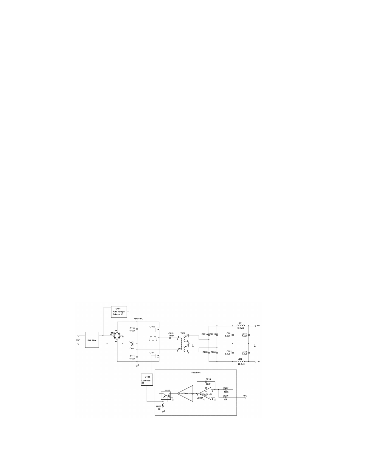
1.2 Functional Block Diagram
Figure 1 shows a block diagram of a switch-mode tracking power supply. Power flows from the AC
line input at left to the DC output at right. Control signal flows from right to left.
Figure 1. Block diagram of a switch-mode tracking power supply
4
Page 5
PS18/28/35 Troubleshooting Guide
Theory of Operation
AC power comes from line source to an EMI filter first, which prevents noise generated by high
frequency switching from flowing back to the line source. A bridge rectifier BR1 converts AC power
into DC power. There are three versions of the power supply; US, Euro, and Dual. For the US
version, the bridge rectifier BR1 is configured to a voltage doubler rectifier. For the Euro version,
the bridge rectifier BR1 is configured to a full wave rectifier. For the Dual version, an automatic
voltage selector IC turns on or turns off the triac Q401 depending on the line voltage, re-configuring the bridge rectifier into a full wave rectifier for 220V/240V line or a voltage doubler rectifier for
100V/120V line. Electrolytic capacitors C110 and C111 filter out line frequency and its harmonics.
A DC voltage at about 340V is obtained across the two capacitors regardless of the line voltage
variation.
The DC voltage is then inverted into a high-frequency quasi-square voltage by two power
MOSFETs Q101 and Q102 which are turned on and off at a high frequency (100kHz ~ 200kHz) by
the controller IC U101. The high-frequency quasi-square voltage is applied to the primary winding
of the center-tap transformer T102 via a capacitor C115. Capacitor C115 and leakage inductance
of the transformer form a resonant circuit, which shapes the resonant current waveform into a
quasi-sinusoidal waveform. The power to the transformer is controlled by adjusting the switching
frequency relative to the resonant frequency. A rectifier connected to the secondary of the transformer converts the high-frequency power into DC power and a low pass filter removes highfrequency contents. DC power is obtained at two output terminals. This circuit which converts DC
power to DC power is called a half-bridge high-frequency resonant DC-DC converter.
A negative feedback circuit made of an integrator, a nonlinear amplifier, an opto-coupler, and a
controller IC controls the above power converter in such a way that the output voltage of the power
converter follows or tracks the power supply control (PSC) signal, which is generated at the DSP
board to track the audio signal.
In addition to the above basic functions, overvoltage, amplifier fault, and over temperature protection circuits are designed to prevent the power supply and amplifiers from catastrophic failure. The
power-down circuit is also designed so that the power supply outputs decay slowly when the AC
input power is turned off. Two linear regulators are tapped off the two output rails to provide two
regulated low voltage rails.
The high-frequency transformer and the opto-coupler provide electrical isolation between the AC
line source and audio circuitry that is powered by the power supply.
Since the transformer is operated at a high frequency, it can be designed to be very small and yet
very efficient. The size of power supply is significantly reduced compared with a power supply
using a line-frequency transformer.
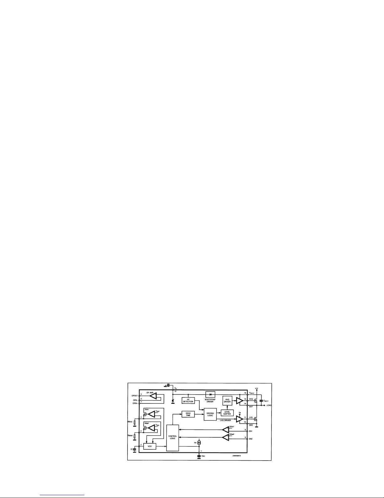
1.3 Resonant Controller IC
This section describes the high-voltage resonant controller IC that controls the resonant power
converter which is the brain of the power supply. Figure 2 shows the block diagram of the IC. Its
main function is to generate a high-frequency signal at a voltage-controlled-oscillator (VCO) and to
drive two power MOSFETs in a half-bridge circuit.
Figure 2. Block Diagram of high-voltage resonant controller IC
5
Page 6
PS18/28/35 Troubleshooting Guide
Theory of Operation
The IC has two enable pins, one of which (pin-8) disables the operation while the other (pin-9)
enables the operation. A voltage pulse higher than 0.6V at pin-8 shuts down the IC and a voltage
pulse higher than 1.2V at pin-9 wakes up the IC. An opamp, an under voltage lockout circuit, and a
soft start circuit are also built into the IC.
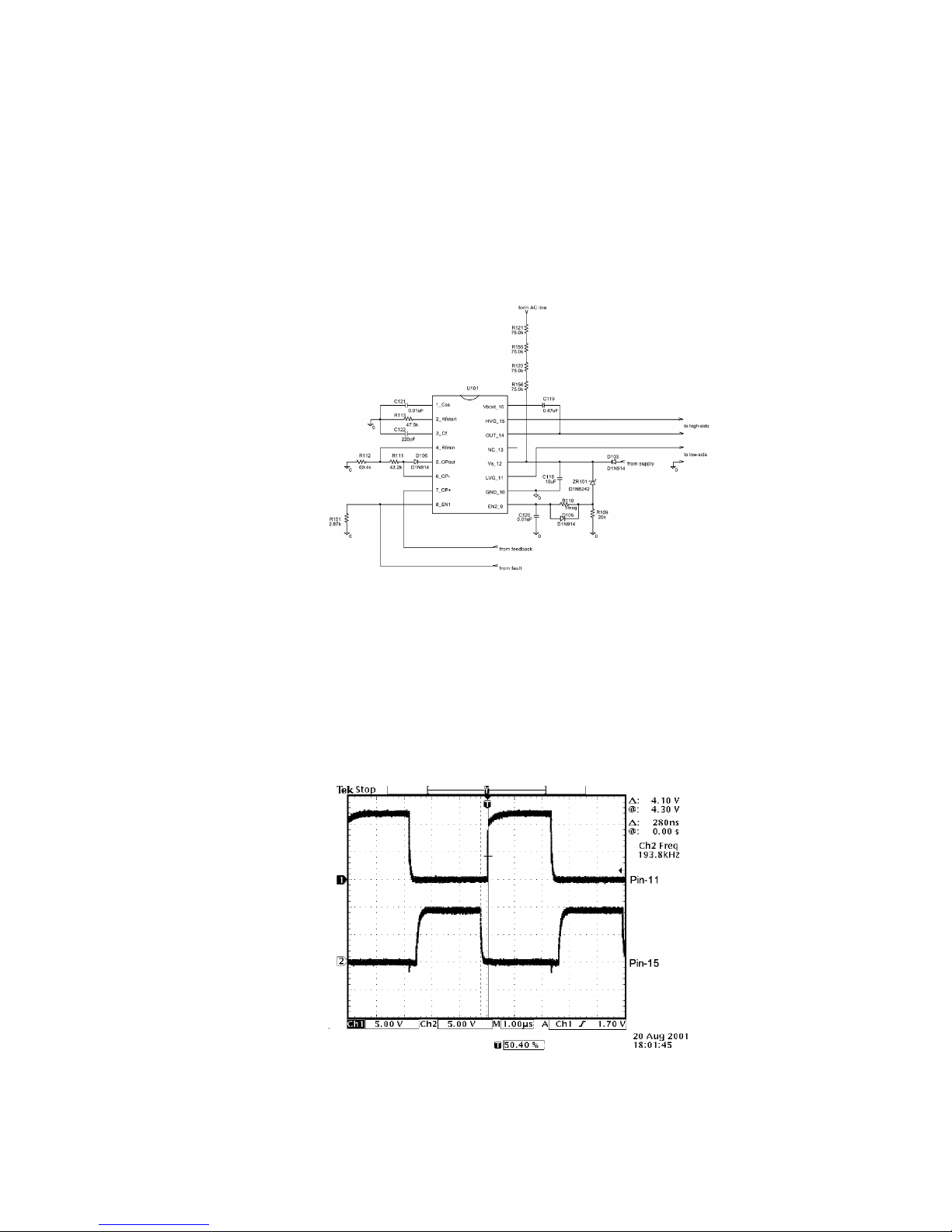
Figure 3 is a circuit diagram that shows how the IC is used in the tracking power supply. With a
12V voltage established at pin-12 (Vs), the VCO starts to oscillate, sweeping oscillation frequency
from its start frequency (350 kHz) downward. A gate-driving signal for a low-side MOSFET is
generated at pin-11 with respect to pin-10, and another gate driving signal for a high-side
MOSFET is obtained at pin-15 with respect to pin-14.
Figure 3. Resonant controller IC used in tracking power supply
Figure 4 shows the oscillograms of the two gate driving signals, when the IC alone is powered on
by a 12V DC supply. A dead time of about 280ns, during which both signals are at low level, exists
between the two gate signals. Such a dead time avoids shoot-through of the two power MOSFETs.
It also allows zero-voltage switching as will be explained later.
The frequency of the two signals is controlled by a voltage at pin-7, which is connected to the
output of an opto-coupler. The frequency is about 200 kHz with 0V at pin-7 and 100 kHz with 2V at
pin-7.
Figure 4. Scope photo of two gate driving signals
6
Page 7
PS18/28/35 Troubleshooting Guide
Theory of Operation
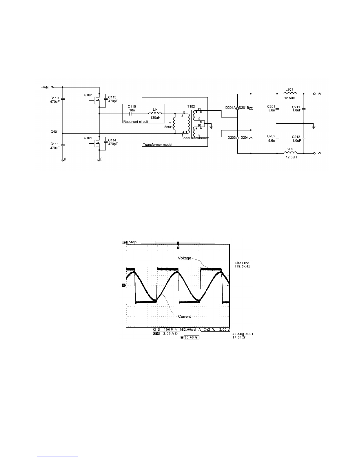
1.4 High-frequency Resonant Converter
This section describes the theory of operation for a high-frequency half-bridge resonant DC-DC
converter, the heart of the power supply. Figure 5 shows its detailed circuit, where the high-frequency transformer is represented by a leakage inductor Llk, a magnetizing inductor Lm, and an
ideal step-down transformer.
Figure 5. High-frequency half-bridge resonant DC-DC converter
With gate signals from the controller IC, the two power MOSFETs Q101 and Q102 are turned on
and off alternately to invert the DC input voltage to a high-frequency square wave voltage. The
high-frequency square wave voltage is applied to a series resonant circuit made of a resonant
capacitor C115 and leakage inductor Llk of the transformer. The resonant circuit shapes the
current waveform to a quasi sinusoidal waveform. Figure 6 shows oscillograms of the voltage
across MOSFET Q101 and current through capacitor C115. Such a smooth current waveform
lowers electromagnetic interference (EMI) emissions from the power supply.
Figure 6. MOSFET Q101 voltage and C115 current waveforms
The transformer transfers high-frequency power from the primary winding to two secondary
windings. The rectifier diodes D201A, D201B, D203, D204 rectify the high-frequency power and
the two capacitors C201 and C202 filter out high-frequency contents. A low pass L-C filter is
added to each rail to further reduce the high-frequency noise. Two DC voltages, one positive and
one negative, are obtained at the output.
7
Page 8
PS18/28/35 Troubleshooting Guide
Theory of Operation
The parameters of capacitor C115 and inductor Llk are selected in such a way that its resonant
frequency is lower than the range of switching frequencies. In other words, the switching frequency
is always above the resonant frequency. The resonant circuit is operated in inductive mode. Two
capacitors C113, C114 are added in parallel with the two MOSFET switches to slow down the
voltage transition across the two switches. Inductive mode operation and a dead time provided by
the IC, shown in Figure 4, allow the voltage across the two switches to transit smoothly from high
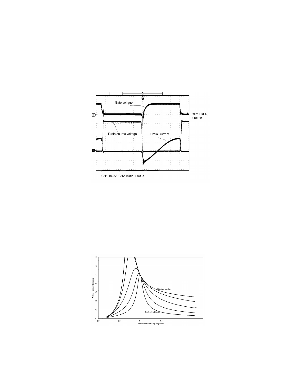
to zero and from zero to high. Figure 7 shows gate voltage, drain-source voltage, and drain current
for MOSEFT Q101. As can be seen from Figure 7, the power MOSFET is turned on and turned off
when its drain-source voltage is zero. Zero-voltage switching like this reduces switching loss and
switching noise.
Figure 7. Gate and drain-source voltage, and drain current waveforms for MOSEFT Q101
A characteristic of a resonant converter arrangement shown in Figure 5 is that the ratio of the
output DC voltage to the input DC voltage is determined by the ratio of the switching frequency to
the resonant frequency of capacitor C115 and inductor Llk. Figure 8 shows a plot of voltage
conversion ratio versus normalized switching frequency. Each of the curves represents a different
load resistance that is equivalent to the two loads at the two output rails. For example with load L3,
voltage conversion ratio decreases with the normalized switching frequency if operated above
resonance (inductive mode). Therefore, by moving the switching frequency away from resonance,
the output voltage is lowered.
Figure 8. Plot of voltage conversion ratio versus normalized switching frequency
8
Page 9
PS18/28/35 Troubleshooting Guide
Theory of Operation
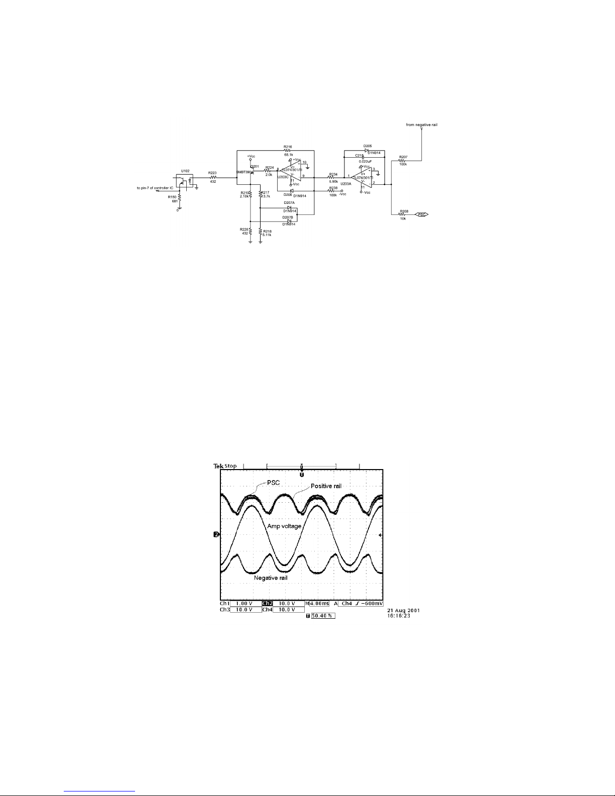
1.5 Feedback Control Circuit
The feedback circuit controls the above power converter in such a way that its output voltage
follows or tracks the power supply control (PSC) signal. This section describes the feedback circuit
shown in Figure 9.
Figure 9. Feedback circuit
The feedback control circuit senses the negative output of the power converter and compares it
with the PSC signal. The error is amplified by an integrator. The amplified error is compensated by
a nonlinear amplifier for loop stability and is then applied to the resonant controller IC via an optocoupler.
If the magnitude of the negative voltage is lower than what the PSC signal demands, the output
voltage of the opto-coupler is higher, lowering the oscillation frequency of the resonant controller
IC. The IC moves the switching frequency closer to the resonant frequency of the power converter,
increasing the magnitude of output voltage. Such a negative feedback control minimizes the error
between the rail voltage and the PSC signal. The voltage at the power supply output terminals
tracks the audio signal. Figure 10 shows waveforms of a PSC voltage, two output voltages, and an
amplifier output voltage for a tracking power supply used as power source for one audio amplifier.
The PSC is derived from the audio signal and an offset is added for voltage drop at the amplifier
(amp saturation voltage). The two rails track PSC very well.
Figure 10. Power supply waveform showing tracking voltage
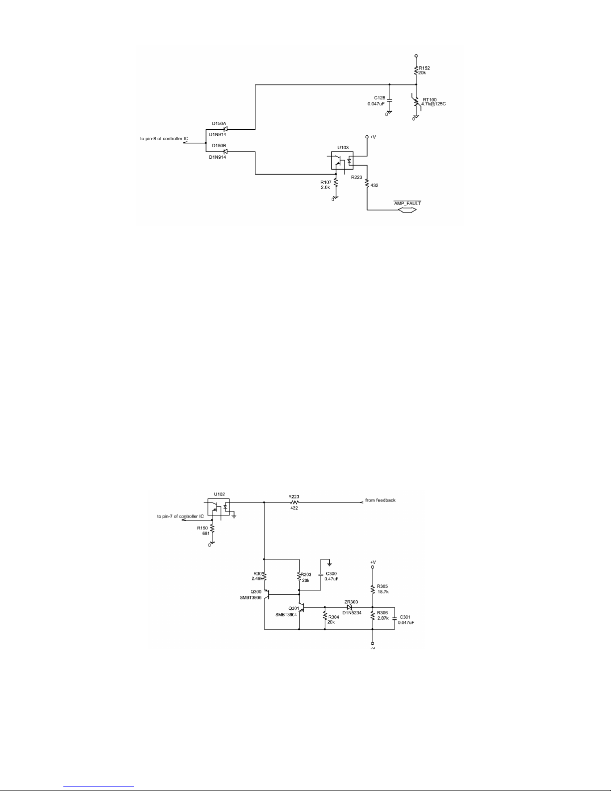
1.6 Protection Circuits and Others
This section describes protection circuits and some other circuits that are added to the power
supply. Figure 11 shows an over-temperature protection circuit and an AMP_FAULT protection
circuit.
9
Page 10
PS18/28/35 Troubleshooting Guide
Theory of Operation
Figure 11. Over-temperature and AMP_FAULT protection circuit
A positive-temperature-coefficient (PTC) resistor RT100 is placed next to a heat sink for two power
MOSFETs. When the PTC RT100 is heated up to 125°C by the heat sink, the resistance of the
PTC increases dramatically, resulting in a logic-high at the PTC. Independently, when any audio
amplifier is in fault condition, the AMP-FAULT is pulled down, setting a logic-high at the output of a
second opto-coupler U103. Either over-temperature or amplifier fault sends a voltage pulse to pin8 of the resonant controller IC, shutting down the IC and hence the power supply.
Referring to the resonant controller IC circuit shown in Figure 3, the Vs-pin (pin-12) of the IC will
be slowly charged up beyond 12V in shutdown mode by a current through R156 since the IC
consumes very little power after it is shut down. Zener diode ZR101 starts conducting, charging
voltage at pin-9 up. Once the voltage at pin-9 reaches 1.2V, the IC is enabled. The power supply
resumes operation. The above shut down and recovery process repeats until both over-temperature and AMP-FAULT conditions are removed.
During normal operation, the resonant controller IC is powered by rectifying the dv/dt current
through capacitor C114 that is connected across MOSFET Q101 (Figure 5).
An overvoltage protection circuitry shown in Figure 12 is designed to protect the rail-to-rail voltage
from exceeding 52V. If the rail-to-rail voltage exceeds 52V, Zener diode ZR300 starts conduction,
activating transistor Q301 and hence transistor Q300. Current to opto-coupler U102 is pulled away.
The consequence of such is a lower rail-to-rail voltage.
A power-down circuit, shown in Figure 13, is designed for the output voltage to decay slowly after
the power switch on the AC line is turned off. Upon detection of low voltage at the AC line, transistor Q104 turns on, turning on transistor Q103. With the turn-on of transistor Q103, the power
converter operates in an open-loop manner. The output voltage of the power supply follows the
Figure 12. Overvoltage protection circuit
10
Page 11

PS18/28/35 Troubleshooting Guide
Theory of Operation
slow decay of the voltage at the two energy storage capacitors C110, C111. The power down
circuit gives the audio power amplifiers enough time to mute before the rail collapses, preventing
the speakers from making a pop noise.
Figure 13. Power down circuit
1.7 Automatic Voltage Selector
An automatic voltage selector is built-in for the dual version of the power supply. Figure 14 shows
the automatic voltage selector, which consists of the automatic voltage selector IC U401 and the
triac Q401. Jumper JP1 is not installed for the dual version. If the AC line voltage is below 170V
rms, IC U401 sends a train of pulses to triac Q401, turning it ON. The rectifier becomes a voltage
doubler. If the AC line voltage is above 170V rms, IC U401 sends a low signal to triac Q401,
turning it OFF completely. The rectifier becomes a full wave bridge rectifier.
For the US and Europe version, all parts for the automatic voltage selector with reference designation 4XX except SMD parts are left empty. For the US version, jumper JP1 is installed and the
choke L103 is not used. For the Europe version, the choke L103 is installed and jumper JP1 is not
used. At either 120V US line or 240V European line, a DC voltage at about 340V is obtained at the
rectifier output.
Figure 14. Automatic voltage selector
11
Page 12

PS18/28/35 Troubleshooting Guide
Theory of Operation
2. DSP PCB
2.1 General Overview
The DSP board contains the majority of the control and signal processing functionality for the
PS28 Powered Speaker. The DSP board receives audio data and SmartSpeaker commands from
the head-end via the RJ-45 connector. There are no analog audio inputs to the bass module; all
audio information comes via S/PDIF input from the head-end. Audio sample rates from 32kHz to
48kHz and PCM, AC-3, and DTS formats are auto-detected and supported.
The DSP is a 4-layer PCB, with all interconnects to the Power Supply PCB and Amp PCB accommodated by J604, a 20-pin card-edge connector. The DSP board has two ground connections to
the die-cast aluminum chassis through “spring fingers” formed by two thin PCB features along the
edge of the PCB. These “fingers” are displaced by mating sloped features on the bottom of the
chassis to make contact when the DSP board is fully inserted into the slots.
2.2 Power Supplies
Sheet 7, 8 of SD254175
“Raw” power for the DSP board is supplied by the Power Supply PCB in the form if “+V” which is
the positive DC supply which “tracks” the audio signal and +/-10VDC regulated. The +/-10VDC is
brought onto the board at J604 pins 11 and 1, respectively, where they are designated as +VCC
and –VCC, respectively. +V is brought onto the DSP board at J604 pins 8 and 18.
+V is solely used to power the 5V switch-mode regulator U501. +VCC and -VCC are used to
power all of the OP Amps (U402, U404, U406, and U407) and +VCC is used to power the LM339
comparator U3.
The 5V switch-mode regulator formed by U501, and associated components, operates by chopping the input voltage (13-24VDC) at 120 kHz and filtering it through a LC lowpass filter. The
resulting output voltage is divided down by R506/R507 and compared against an internal 3.3V
reference in U501, which modulates the pulse width to maintain a regulated 5.0V across C517.
When the switching regulator is running, the PWM waveform can be observed at pins 5/6 of U501
using an oscilloscope. R505 and D502 are required to prevent the tracking power supply from
“seeing” the 330uF of capacitance at C519, since the +V voltage varies at audio rates between
approximately 13V and 24V.
The regulated 5V output is used to generate the 2.5V and 3.3V supplies. The 3.3V supply is
generated using a fixed-voltage 3.3V linear regulator, U502. The 2.5V supply is generated using a
LM317-series adjustable voltage regulator. R509/510 divide down the output voltage being fed
back to the regulator to generate the required 2.5V on the output.
2.3 DSP, FLASH PROM, and SDRAM
Sheet 3 of SD254175
The fundamental heart of the DSP board and LS28/35 bass module functionality is rooted in the
Analog Devices 21065L Sharc DSP processor (U4) and the RAM (U302 and U303) and PROM
(U301) associated with it. The Sharc DSP is a floating point processor capable of approximately
60MIPs performance and runs typically at 53-55 MIPs. The Sharc provides all control and “housekeeping” functions for the hardware and software as well as all signal processing, except decompression of AC-3 and DTS formats (this is done by the CS49329, U103). Note that on the sche-
12
Page 13

PS18/28/35 Troubleshooting Guide
Theory of Operation
matic SD254175, that the Sharc, U4, has been schematically broken up into several blocks of
similar function/connection pins to make the schematic easier to follow.
The DSPs have no internal program ROM, so all executable program code must be stored in
external ROM. This function is provided by U301, a 4Mbit FLASH PROM. This FLASH is programmed at In-Circuit test of the DSP board. The FLASH also contains a Parameter Block, which
holds unit specific information, such as EQ type to implement (Double Satellite, Jewel
speaker, etc.), tracking power supply calibration info, tone control curve type, etc.
Two Synchronous Dynamic RAM ICs (U302 and U303) are also attached to the Sharc’s parallel
bus. These are used as real-time RAM for the DSP.
The Sharc, FLASH, and SDRAM are all linked together with a 32 bit data bus and 20 bit address
bus, as well as the necessary handshaking and flow control lines, from the Sharc. Also on the
lowest 8 bits of the data bus is a 74LCX244 multiplexor IC which allows eight additional input/
output lines to be connected to the Sharc. These lines are used for various handshaking, serial
communications, and status info communications with the other hardware on the board. Because
this single address and data bus structure contains all the key components of the DSP board, any
shorts, opens, bridges, or damaged components on any of these lines will cause the DSP to
function incorrectly, or, most likely, not at all.
®
cube
The clock for the Sharc and data bus are generated by the onboard crystal oscillator of U4 (Sharc)
and Y201. The internal instruction clock for the Sharc operates at 2x the oscillation frequency of
Y201. Because this is the sole source of clocking for the DSP, if this clock does not function, the
DSP will cease to function at all.
The Sharc, SDRAM, and FLASH all operate off the 3.3V supply rail.
2.4 Serial data interface, SmartSpeaker and TAP
Sheet 1 of SD254175
The SmartSpeaker interface to the head-end is a single wire, bidirectional serial data interface that
operates at 4800 baud, 1 start bit, 8 data bits, no parity, and 1 stop bit. The bus is open-collector,
with pull-up on the DSP board to 3.3V. This signal is connected to the head-end via pin 1 of J1.
The ground reference/return for all serial communications is pin 2 of J1.
Pins 3 and 6 of J1 form the serial RCV and XMT connections for TAP communications. Unlike
previous Lifestyle bass modules, the bass module communicates in RS-232 compliant format,
such that a TTL-to-RS232 converter is not needed. TAP communications operate at 4800 baud, 8
bits, even parity, 1 stop bit.
Two sections of the LM339 comparator U3 are used to form the serial data receivers. Since both
the TAP and SmartSpeaker receive lines share the same input line on the Sharc, only one communications mode can be supported at any given time.
13
Page 14

PS18/28/35 Troubleshooting Guide
Theory of Operation
The unit boots into SmartSpeaker mode by default and can be put into TAP mode via two different
methods:
• Send out the following 4 bytes using a RS-232 terminal (4800 baud, 8 bits, no parity, 1 stop bit):
0x01,0xFF,0xAA,0x54. This tells the board to switch to ASCII TAP mode. The board will then switch
protocols to 4800 baud, 8 bits, even parity, 1 stop bit. It will reply with a single ‘>’ (0x3E). Since the
response is 0x3E, the parity bit will be set to 1; there is no need to switch protocols until after the
‘>’ is received since the parity bit will look like a stop bit. Switch the RS-232 terminal to 4800 baud,
8 bits, even parity, 1 stop bit. At this point, normal ASCII TAP commands can be sent to the board.
Note that when TAP mode is activated in this manner, the DSP will not echo characters sent by the
terminal.
• Set all four DIP switches into the “up” position (away from RCA plugs). Power the PS28 up using
the AC line switch and wait until the amber LED blinks twice and the green LED blinks briefly at
least once (approx. 3 seconds after power up). Then, within twenty seconds, flip ALL four switches
down, then flip switch #4 (closest to the RJ-45 connector) back up. The unit will now communicate
in TAP mode. Note that when TAP mode is activated in this manner, the DSP will echo characters
sent by the terminal.
2.5 Thermistor Temperature Sensor
Sheet 8 of SD254175
RT600 is a negative temperature coefficient device which is used to measure the ambient temperature in the vicinity of the DSP. This measured temperature is used by the DSP in a complex
algorithm which uses the woofer output signal and the PSC_PWM signal (which contains info
about the power supply rail voltage) to compute the power being dissipated in the MOSFETs on
the Power Supply PCB and, hence, their approximate temperature, then adjusts the system gain
over time to keep the unit’s operating temperature within safe limits despite the external ambient
temperature or how long/loud the unit has played. This algorithm only “turns the volume down” by
a few dB in cases where the unit has been operated at maximum volume levels with “heavy”
source material.
The resistance of RT600 changes inversely proportional to the temperature of the device, with its
resistance nominally 10k at room temperature (25°C). The circuit formed by two of the comparator
sections of U3 and the associated parts form an oscillator which has an “on” time determined by
C620 charging through R655 and an “off” time determined by C620 discharging through RT600.
This makes the oscillator output a waveform with a duty cycle that is a function of the temperature
of RT600. The DSP samples the output of the oscillator at a constant rate and averages the total
“on” time and total “off” time over 10 cycles of the oscillator to compute the temperature.
2.6 DIP Switches
Sheet 8 of SD254175
The 4-position DIP switch S1 is primarily on the DSP to set the room code of the bass module for
situations where there are multiple speakers on a single zone of a Lifestyle
switches normally ship with all four in the “down” position (towards the PCB). They also serve as a
method of setting the Sharc into TAP mode, but only during the first 20 seconds after power has
been turned on.
14
®
media center. These
Page 15

PS18/28/35 Troubleshooting Guide
Theory of Operation
2.7 LEDs
Sheet 8 of SD254175
The amber and green LEDs on the DSP board serve to provide a wealth of information about the
status and operation of the DSP board. The following is a summary of the various possible states
of the LEDs and a functional description of the state(s) represented.
• Green LED: The green LED serves a dual purpose: general system health and serial data re-
ceived. The green LED will blink once per second with a 50% duty cycle (i.e. on for ½ second, off
for ½ second) if the system booted and is running normally. If the unit is in the SmartSpeaker “Off”
condition, the green LED will blink briefly (approx. 0.1s ON time) once every 5 seconds.
• The green LED will also toggle whenever a serial data byte is received. This will interrupt the
normal 1 second blink rate. The green LED blinking faster than 1 Hz usually indicates that it is
receiving serial communications.
• Amber LED: The amber LED serves to signal 3 conditions: power applied/boot status, S/PDIF
status and clipping status. When power is first applied the amber LED will light briefly. If the PROM
FLASH checksum is incorrect or hardware does not pass power-on self test, the green LED and
amber LED will alternately blink at approximately a 5 Hz rate. If the green LED is blinking at its
normal, 1 Hz rate, a blinking, 1Hz amber light indicates that there is no valid S/PDIF signal
present: If the amber LED is off while the green LED is blinking normally, then valid S/PDIF is
present and being received. Finally, if the amber LED will briefly blink (in this case, only when valid
S/PDIF is present) when the satellite amps are clipping. This should only occur when playing the
system at very high levels.
2.8 Master Reset and Watchdog Timer
Sheet 8 of SD254175
U602 functions as the master Reset controller and watchdog timer. This part will briefly issue a
Reset to the Sharc when the +3.3V rail first comes up or if the 3.3V rail drops below 3.08V. The
part also contains a timer which will cause a Reset to occur approx. every 1.5 seconds unless the
WDI input to the IC is toggled at least once during each 1.5 second cycle. This is useful in the
event that the Sharc would become “lost” in program execution, which would prevent it from “petting” the watchdog every second, and the system would get Reset and recover.
2.9 Tracking Power Supply Control Output
Sheet 3, 8 of SD254175
As part of the DSP signal processing, the maximum level of any of the six audio channels in a
256-sample block is computed. This value is then translated into the minimum required power
supply rail voltage needed by the power amplifiers to reproduce that block of audio without clipping
or distorting. The Sharc adjusts the duty cycle of the pulse-width modulator output DT1B (pin 23)
of U4 appropriately so that the resulting “DC” voltage after the RC lowpass filter formed by R209/
217 and C203 is 1/10
the Power Supply PCB through J604, pin 12. When there is no audio output (or relatively low
levels), this output should be at 0% duty cycle, or approx. 1.3V as measured at PSC_PWM.
th
the required power supply rail voltage. This signal, PSC_PWM, is sent to
15
Page 16

PS18/28/35 Troubleshooting Guide
Theory of Operation
2.10 Bass and Satellite Clip Detect Inputs
Sheet 3, 8 of SD254175
The Power Amplifier board has circuitry to predict signal clipping of the amplifier outputs on positive going peaks. These events are separately sensed for the Bass channel and the satellite
channels (all 5 are logic-OR’d together) and brought on to the DSP board through J604. They pass
through RC lowpass filters and connect directly to the Sharc’s IRQ1 and IRQ2 inputs. At this time,
these inputs have no effect on the signal processing other than briefly lighting the amber LED
whenever a satellite clip event occurs. The DSP’s soft-clipper and limiter algorithms perform all of
the compression and gain limiting functions normally associated with feedback limiters. In the near
future, this circuitry will be removed from the Amp and DSP boards for cost savings.
2.11 S/PDIF Receiver
Sheet 1 of SD254175
The only audio input for the bass module is through the differential (balanced) S/PDIF input on
pins 7,8 of J1 (RJ-45 connector). The S/PDIF signal is coupled into the unit via bypass capacitors
(C609/610) to the chassis and SMD ferrite beads (FB3/4) to help alleviate EMI problems. A DC
blocking capacitor, C18, prevents DC currents from saturating the coupling transformer T1. T1 is a
broadband pulse transformer with a 1:1 turns ratio which performs the function of isolating the
incoming signal as well as balanced-to-unbalanced conversion. The secondary of T1 is connected
to a pair of back-to-back diodes that provide the “termination” for the input signal. This allows long
runs of wire and unknown transmission line impedances to exist between the head-end and bass
module and still be able to recover the S/PDIF signal. The clamped signal is fed into a resonated
LC lowpass filter which provides a sharp roll off at approximately 8 MHz. This allows S/PDIF data
at up to 48 kHz sample rate to pass through, but sharply attenuates out of band noise and transients which might cause interruptions in the S/PDIF data stream. This filtered, single-ended signal
is then fed into the RXP0 input (pin 4) of the CS8415A (U2). The RXP0 and RXN0 inputs are
internally biased to approx. 1/2Va (or approx. 2.5V). Both of these inputs are AC coupled through
capacitors.
The CS8415A (U2) recovers the serial audio data clocks by using a PLL, whose DC detector
output is filtered by the components attached to pin 8, R17 and C8/9. These audio clocks are
master for the function of the rest of the audio signal processing chain and DACs.
The CS8415A communicates setup and status information to/from the Sharc via an I2C port using
the SDA and SCL signals.
The status of the EMPHASIS bit in the S/PDIF stream is reflected on the /EMPH output, pin 3 or
U2. This line is connected to the Sharc (U4) and allows the appropriate de-emphasis to be performed on signals which have pre-emphasis.
Errors and problems with the incoming S/PDIF stream are signaled to the Sharc in two ways. The
RERR output (pin 11) of the CS8415A is connected via Q8 and R219 (forming a logic inverter) to
IRQ0 of the Sharc (U4) so that problems with the audio data stream can be quickly detected and
the audio outputs muted before pops, clicks, etc. can be heard. The RERR pin is also logic-OR’d
with the output of a simple “missing-pulse detector” formed by Q7. This signal, 8415_CLKERR,
goes high when either the CS8415A has detected a problem or the LRCLK (serial audio data
frame clock) has stopped. This 8415_CLKERR signal also goes to the Sharc (U4) through the
multiplexor U601.
16
Page 17

PS18/28/35 Troubleshooting Guide
Theory of Operation
Serial audio data comes out of U2 on pins 10, 16, 17, and 18. The audio master clock,
SPDIF_256FS clocks at 256 times the audio sample rate.
The analog receiver section of the CS8415A operates off the +5V supply rail and the digital/logic
sections operate off the +3.3V supply rail.
2.12 Compressed Audio Decoder
Sheet 2 of SD254175
Serial audio data and clocks from the CS8415A S/PDIF receiver are piped to the CS49329 Decoder DSP, U103. This IC operates in one of three modes, depending on the type of data being
received. When the type of data coming in is detected, the firmware corresponding to the type of
decoding necessary is downloaded to the CS49329 from the Sharc. Once this appropriate decoder program is running in U103, the decoder will output the decompressed audio (or in the case
of stereo PCM, pass it through) on the lines 49300_AUDATA0-2, along with corresponding clocks
49300_64FS and 49300_LRCLK. The clock signals and 49300_AUDATA0 are buffered by U105,
since they drive multiple inputs on the Sharc.
The CS49329 (U103) is controlled and program code downloaded from the Sharc via an 8 bit
parallel bus and associated handshaking lines. U103’s processor clock is derived from the clock
input node labeled “10 MHZ”, which is created by the Sharc’s PWM1 output. This clock actually
runs at 7.5 MHz. The CS49329 also has an onboard PLL for clock generation which utilizes R106
and C106/108 for detector output filter.
The CS29329 operates solely off the +2.5V supply rail. It also has separate analog and digital
supplies and each individual supply pin(s) are decoupled with ferrite beads and bypass capacitors.
The digital inputs and output of the CS49329 are all 3.3V-logic compatible, allowing it to interface
with the 3.3V Sharc and S/PDIF receiver.
2.13 Audio Codec
Sheet 5 of SD254175
The audio codec, U401, is a CS4428A, which has stereo A-to-D converters and six D-to-A converters on it. As implemented the A-to-D converters are not used. In fact, they are powered down
using an I2C control register in the part.
The codec is controlled via an I2C interface which allows the Sharc to program the device’s control
registers and read back status information from the device. The digital audio information is read
into the codec via 3 two channel serial data lines (4228_SDIN1-3) and their associated bit and
frame clocks, 49300_64FS and 49300_LRCLK, respectively. The master, 256*Fs clock in run off of
the SPDIF_256FS output from the CS8415A S/PDIF receiver IC (U2).
The circuitry hanging off the codec’s analog inputs (pins 16, 17, 19, & 20) is unused in the current
application. This circuitry was intended to allow the unit to measure its own Left output channel in
order to perform self-diagnostics and calibration of the tracking power supply. The calibration of the
tracking power supply is currently performed when the unit is manufactured.
The analog inputs and outputs of the codec are internally biased and referenced around (nominally) 2.3V. This internal reference voltage is brought out at pin 18 (FILT) and bypassed to ground
by C407. Since this pin is a high impedance output, no current can be drawn from it without adversely affecting the codec’s performance. To match the external circuitry to the analog outputs,
17
Page 18

PS18/28/35 Troubleshooting Guide
Theory of Operation
one section of U402 is used to buffer a 2.3V reference derived from the regulated 5.0V supply.
This external analog reference voltage is marked as “DC_BIAS” on the schematic.
The codec has a mute control output, /MUTEC, which it asserts (active low) immediately whenever
it detects problems with incoming clocks or data and the outputs may become unpredictable (i.e.,
pops, clicks, noise, etc.). This signal is logic-AND’d with the other mute signals from the Sharc that
control the power amplifiers. See the section on MUTE control for more details.
The codec’s analog sections operate from +5V supply rail with a ferrite bead and bulk capacitance
decoupling. The digital section is fed from the +5V supply, also. The logic interface section is fed
from the +3.3V supply to interface with the 3.3V-logic Sharc.
2.14 Codec Output Buffers and Low Pass Filters
Sheet 6 of SD254175
The six audio outputs from the codec’s DACs are fed into differential amplifiers with a gain of 3.65
(11.25dB) which subtracts out the DC bias of the codec and references the audio signal to the
ground of the power amplifiers. The power amp reference is accomplished by one section of U402
OP Amp which buffers the ground signal “AMP_GND” which is sourced from the Power Amp PCB
via J604, pin 13. This buffered amp ground reference is marked as “GND_REF” on the schematic.
After the audio signals are referenced to the power amplifier’s ground, they are passed through a
second order Low Pass filter with a corner frequency of approx. 27 kHz. These lowpass filters are
used to reduce the amount of out-of-band DAC artifacts that get sent to the power amplifiers and
out onto the speaker lines. The outputs of the six LPFs are then passed through a 300 Ohm,
100pF RC lowpass filter for EMI filtering to the Power Amp PCB via J604.
The OP Amps used for the buffers and LPFs are operated off of the +/-VCC supplies (+/-10V).
Maximum (full-scale) audio output from DSP board is approximately 6.8Vpeak (4.8Vrms).
2.15 MUTE Controls
Sheet 8 of SD254175
The Sharc uses its FLAG5 and FLAG6 outputs to separately control the muting of the Right/Left/
Center/Bass amplifiers and Surround amplifiers, respectively. These mute signals are logic-AND’d
with the /MUTEC control output of the codec to provide comprehensive control of the power
amplifiers mute. The Sharc will assert the mute lines (active low) under the following conditions:
• When 5-Speaker mode is NOT selected, the /LSRS_MUTE is asserted. This keeps the rear
channels from making any sound or background “hiss”.
• When no S/PDIF signal is present. i.e., no audio.
• When the bass module is in the SmartSpeaker “OFF” state.
• When there has been a S/PDIF error, interruption, or sample rate change. Through the use of the
S/PDIF error detection methods discussed in the S/PDIF receiver section, the Sharc can “panic
mute” the power amplifiers when conditions occur that might cause undesirable artifacts to come
out of the speakers. During this process, the PSC_PWM signal is also immediately sent to its
minimum value.
18
Page 19

PS18/28/35 Troubleshooting Guide
Theory of Operation
2.16 Audio Signal Path Flow
All audio input must come into the bass module via the S/PDIF input on the RJ-45 connector. This
signal is received and converted into two channels of audio data in serial format using a single
data line that carries both the left and right audio sample data, one after another, a frame clock (to
tell whether the data is right or left), and a bit clock. The S/PDIF receiver also generates a Master
audio clock, running at 256 times the audio sample rate. Also, useful information embedded in the
S/PDIF stream, such as pre-emphasis on/off and compressed data on/off, are stripped out and
communicated to the Sharc.
The two channels of audio, whether they are stereo PCM information or compressed multichannel
audio, are sent to the CS49329 (U103) Compressed Audio Decoder. The format of the incoming
data is determined and the Sharc downloads the appropriate decompression program to the
CS49329 (either PCM pass-thru, AC-3, or DTS). The CS49329’s DSP then performs the necessary decompression and recovery of the audio data and sends up to 6 channels of audio out on
three separate serial data lines, using the same serial format as the S/PDIF receiver.
The up-to-six channels of audio from the CS49329, along with their corresponding audio clocks
are inputted into the Sharc, where Videostage® processing, equalization, dynamic equalization,
limiting, tone controls, volume, etc. are performed on them. The audio data is processed in 256
sample blocks such that one block of audio data is being fed out to the D-to-A converter while the
next block is being processed.
The Sharc sends the up-to-six channels of audio out to the audio codec whose D-to-A converters
generate the analog audio signals that end up at the audio power amplifiers.
2.17 Signal Processing
The details of the signal processing are beyond the scope of this document, and only a general
overview of the processing is presented here. There are no user controls on the bass module as
all volume, tone, etc. control is accomplished via the head-end and remote control.
The basic signal processing (EQ and Videostage 5) are essentially identical to that used in the
Lifestyle
®
Series II digital bassboxes. As with the Series II systems, volume and tone control,
dynamic equalization, etc. all accomplished in the digital domain. The compressed format audio
streams (AC-3 and DTS) are decoded by a separate DSP from the Sharc used to perform the
Bose® processing.
2.18 Power On and Boot Up Sequence of Events
When power is first applied, the Sharc boots and loads/executes the first set of instructions found
in the FLASH memory. This code is very basic and only runs power on self tests (POST) that
check basic communications with all the hardware peripherals (U2, U103, U301, U302, U303, and
U401) and computes the version and checksum of the code in FLASH. If all appears to be “well”,
the Sharc reboots and loads the actual program code that makes it function as a LS28/35 bass
module. If the POST fails, the Sharc signals this by rapidly flashing (approx. 3Hz rate) the amber
and green LEDs alternately for a couple of seconds and then performs a Reset and tries again.
19
Page 20

PS18/28/35 Troubleshooting Guide
Theory of Operation
Assuming that the POST is successful, the Sharc sets up the registers for the S/PDIF receiver
(U2), codec (U401), and Compressed Audio Decoder (U103) to function as needed. The
PSC_PWM control is set to its minimum value, the amplifier Mute control lines LRCB_MUTE and
LSRS_MUTE are asserted (low).
After the POST has been successful and the program code is running, the DSP is initially in the
SmartSpeaker “Off” state and polls the serial communications input for valid SmartSpeaker commands. It flashes the green LED briefly once every 5 seconds to signal that it is on and in the “Off”
state.
2.19 Power Down Sequence
Since the bass module never really “shuts off” (it only puts the audio power amplifiers in Standby
mode when sent the SmartSpeaker “Off” command), the only thing that happens when an “Off”
command is received is to start sending all zero data to the D-to-A converters and mute the power
amplifiers.
When power is lost, the DSP is eventually put into Reset by the master reset IC U602 when the
3.3V supply drops below 3.08V. When power comes back, the process described in “Power On
and Boot Up Sequence of Events” will occur.
3. Amplifier PCB
The amplifier board consists of three integrated dual amplifier ICs that provide the six channels of
required amplification. This IC, the TDA7265 manufactured by ST Microelectronics, has thermal
and short-circuit protection built-in. The five satellite channels directly use the output of these
amplifier chips, whereas the bass channel, due to its need to deliver high current, is buffered (in
complimentary emitter-follower configuration) by power transistors Q601 and Q602. These transistors provide the necessary current gain required to drive the low impedance bass speaker.
All six amplifier channels have a voltage gain factor of 3.5 (11.0 dB) with flat frequency response.
3.1 Mute Circuit
The amplifier chips operate in standby mode (no output and low power consumption) until the
mute pin (pin 5) is pulled 6 volts below the +V power supply (pin 3). This is accomplished by
current source transistor Q401 for the surround amp IC (U1) and Q603 for all other channels (U2
and U3). These current sources are controlled by the DSP board mute lines LSRS_mute and
LRCB_mute. These signals are either 0 VDC (muted) or 3.3VDC (unmuted).
If the positive supply rail falls below 9 volts the amplifier chips will mute. This feature is primarily
used to prevent turn-on or turnoff pop. Under this condition, diode ZR2 and transistor Q604 turnoff
and this in-turn causes unmute transistors Q401 and Q603 to turnoff.
3.2 DC Offset Circuit
All six amplifier channels are summed together through 100K resistors (R105, R506, R605,
R305,R405,R609) and low pass filtered by capacitor C1 to create an average DC voltage that is
normally 0 VDC. If a fault condition occurs, where any one or more amps experience a sustained
DC shift of more than 5 volts, transistor Q1 (for a positive fault) or Q6/Q7 (for a negative fault) will
turn-on and pull-down J2 pin 24 voltage from 5 Volts to 0 Volts. This signals the power supply
board that there is a fault condition.
20
Page 21

PS18/28/35 Troubleshooting Guide
Theory of Operation
3.3 Clip Detect Circuit
The satellite clip detect circuit consists of diodes D401, D101, D301 and transistors Q3 and Q4
(upper left section of sheet 2). Q4 and Q3 are normally OFF. At high volume levels, if any one of
the satellite amplifier outputs comes within 2 volts of the positive power supply rail, Q4 and Q3
turn ON and signal the DSP board through SAT_CLIP that compression is needed.
Similarly, the bass clip detect circuit consists of transistors Q5 and Q2. Note: this circuit has been
deleted in later production, due to the DSP board making its own determination as to whether a
clip condition exists.
21
Page 22
PS18/28/35 Troubleshooting Guide
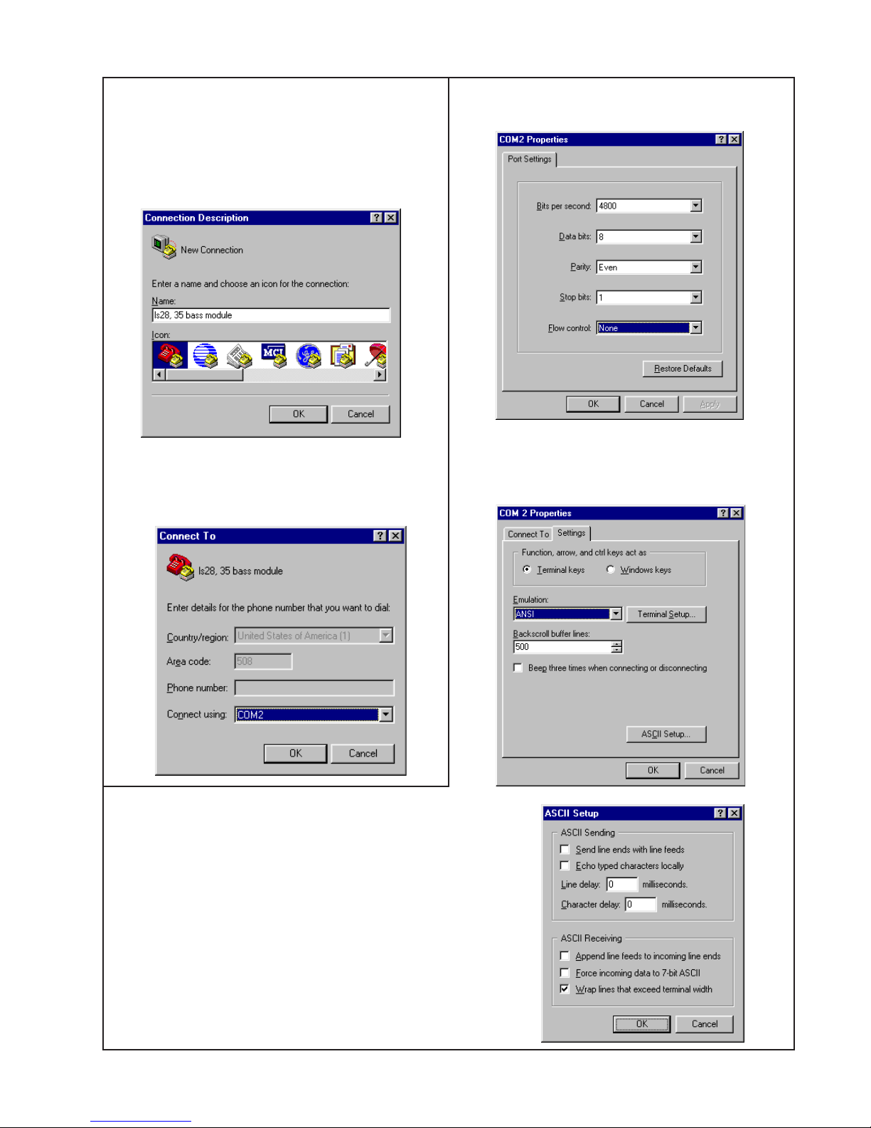
Setting up a computer to issue TAP commands
1. Open a terminal window. Click: Start/Pro-
gram/Accessories/Hyperterminal/Hyperterminal
2. In the “Connection Description” window, type
the name “LS28, 35 bass module test” then
click “OK”; any name may be entered.
3. In the “Connect To” window, select the COM
port on your computer that you will be connecting the bass module to and then click OK.
4. In the “COM1 Properties” window, make the
selections in the various fields as shown.
5. In the Hyper Terminal window, click on File/
Properties. In the Properties window, click on
the Settings tab, make the selections in the
various fields as shown.
6. In the Settings window, click on
ACSII setup and make the selections and changes as shown
22
Page 23

PS18/28/35 Troubleshooting Guide
Placing the Bass Module into TAP Mode
! Place all four DIP switches to the down position before returning the unit to the customer !
1. Place the bass module into TAP mode
1.1 Set all four DIP switches into the “up”
position. Apply power to the bass module using
the AC line switch and wait until the amber
LED blinks twice and the green LED blinks
briefly at least once (approximately 3 seconds
after power up). Then, within twenty seconds,
flip ALL four switches down, then flip switch #4
(closest to the RJ-45 connector) back up. The
unit will now communicate in TAP mode. The
amber and green LED will blink alternately
when no S/PDIF signal is applied. Note that
when TAP mode is activated in this manner,
the DSP will echo characters sent by the
terminal.
UP
12
3
4
Down
2. Verify the bass module communicates in
TAP mode.
2.1 Connect the test cable’s, part number
264564, DB-9 connector to the RS-232 COM
port on your computer. Connect the test cable’s
RJ-45 connector to the bass module.
2.2 Type the command ST S and hit “Enter”.
The following response should be seen on your
computer screen. The results may differ depending on the unit settings. If no S/PDIF
signal is applied, the sample rate will be 29
kHz.
SAMPLE RATE : 44101.30
SPKR TYPE : 02
DIP VALUE : 1111
LCRB_MUTE : 1
LSRS_MUTE : 1
SAT_CLIP : 1
BASS_CLIP : 1
EURO_BASS : 1
EURO_TREBLE: 0
Figure 1. DIP switch Up/Down orientation
Equalizer Programming Method
Type the equalization setup command
SE [SPEAKER TYPE], [EUROPEAN BASS],
[EUROPEAN TREBLE]
ConditionCommand
SPEAKER
TYPE
SE F = falcon ON/OFF ON/OFF
D=doubleshot
C=cricket
B = dublin
M=mariner
U=Installer
Example: To set the equalization to cricket
cubes, euro bass off and euro treble off, type
the command as follows. SE C,OFF,OFF
EURO
BASS
EURO
TREBLE
2.3 Check the software by typing (issuing) the
command TN 4 and then hitting “Enter”. A
typical response would be as follows.
03DE6455, 010808
03DE6455 is the checksum
010808 is the software version
Verify the changes have been made by typing
the command ST S.
The speaker type (SPKR TYPE) and other
information will be displayed. Decode the
numerical two digit speaker type as follows.
00 Falcon (Early version dual cube)
01 Doubleshots (Later version dual cube)
02 Cricket (Jewel® Cube)
03 Dublin (Single Cube)
04 Mariner (151 environmental speakers)
05 User EQ (Installer)
23
Page 24
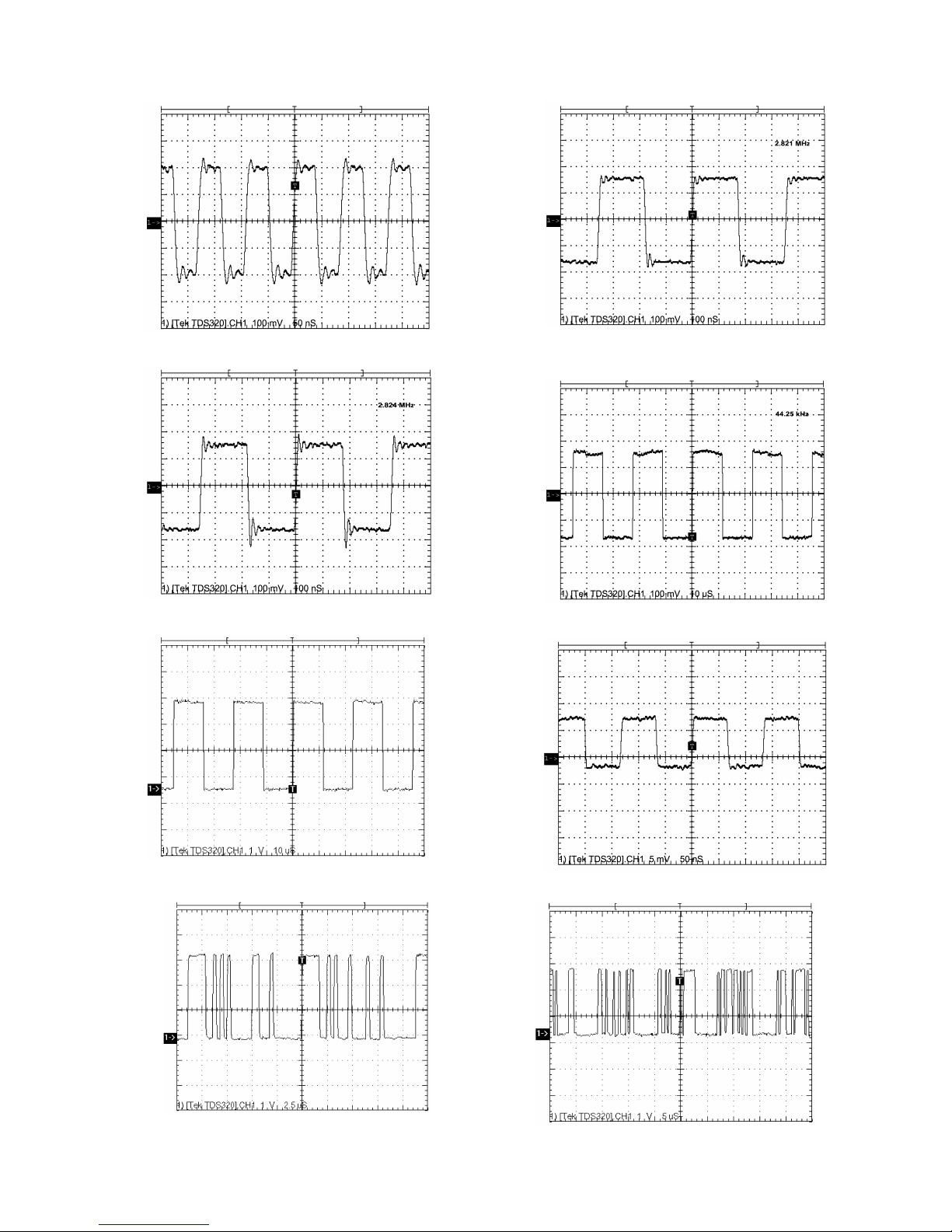
Scope Photos
(x10 probe used)
PS18/28/35 Troubleshooting Guide
DSP PCB, U2 Pin 10, S/PDIF _256FS
DSP PCB, U2 Pin 16, S/PDIF _64FS
DSP PCB, U103 Pin 25, S/PDIF _64FS
DSP PCB, U103 Pin 26, S/PDIF LRCLK
DSP PCB, U2 Pin 17, LRCLK
DSP PCB, U2 Pin 18, SERIAL DATA OUTPUT
DSP PCB, U103 Pin 30, 10 MHZ (7.5 MHZ
Clock)
DSP PCB, U103 Pin 41, AUDATA0
24
Page 25
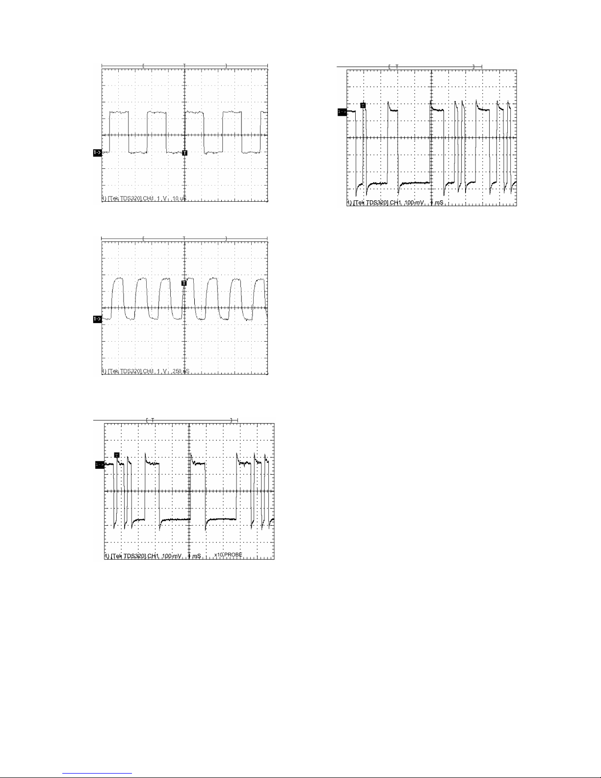
Scope Photos
(x10 probe used)
PS18/28/35 Troubleshooting Guide
DSP PCB, U103 Pin 42, LRCLK
DSP PCB, U103 Pin 43, _64FS
DSP PCB, Q6 Collector, Serial Data XMT.
DSP PCB, U3 Pin 13, SERIAL DATA RCV.
25
Page 26

Pin
Connection
Integrated Circuit Diagrams
ABY
IN+ (1)
IN- (1)
GND
IN- (2)
IN+ (2)
-Vs
MUTE
OUTPUT (2)
+Vs
OUTPUT (1)
-Vs
TDA7265, power amp, 2 x 25W
part number 256084-001
CS8415A, SPDIF receiver
part number 254193-001
1A
1
1B
2
1Y
3
4
2A
2B
5
6
2Y
PS18/28/35 Troubleshooting Guide
14
Vcc
13
4B
4A
12
11
4Y
3A
10
3B
9
Truth Table
LLL
LHL
HLL
HHH
1 Output 2
2 Output 1
3V+
4INPUT15INPUT1+
6INPUT27INPUT2+
8INPUT3-
9INPUT3+
10 INPUT411 INPUT4+
12 GND
13 OUTPUT 4
14 OUTPUT 3
LM339, voltage comparator
part number 187618-001
GND
7
8
3Y
And gate, quad 2-input, CMOS
part number 256124-001
26
Page 27

PS18/28/35 Troubleshooting Guide
Integrated Circuit Diagrams
DSP ADSP21065LKS
part number 254191-001
Pin Type Function
ADDR 23-0 I/O/T
DATA 31-0 I/O/T
___
3-0
MS
___
RD
___
WR
___
SW
ACK I/O/S
_____
SBTS
___
IRQ, 2-0
O/T
I/O/T
I/O/T
I/O/T
I/S
I/A
External Bus Address
memory and peripherals on these pins. In a multiprocessor system the bus
master outputs addresses for read/writes of the internal memory or IOP
registers of other ADSP-21065L. The ADSP-21065L inputs addresses when
a host processor or multiprocessing bus master is reading or writing its internal
memory or IOP registers.
External Bus Data.
on these pins. The external data bus transfers 32-bit single-precision floating-point
data and 32-bit fixed-point data over 31-0. 16-bit short word data is transferred
over Bits 15-0 of the bus. Pull-up resistors on unused DATA pins are not
necessary.
Memory Select Lines
corresponding banks of external memory. Internal ADDR25-24 are decoded into
MS 3-0 . The MS 3-0 lines are decoded memory address lines that change at the
same time as the other address lines. When no external memory access is
occurring, the MS 3-0 lines are inactive. They are active, however, when a
conditional memory access instruction is executed, whether or not the condition is
true. Additionally an MS O which is mapped to SDRAM may be asserted even
when no SDRAM access is active. In a multiprocessor system, the MS 3-0 lines
are output by the bus master.
Memory Read Strobe.
from external memory devices or from the internal IOP register of another ADSP21065L. External devices (including other ADSP 21065L’s) must assert RD to read
from the ADSP-21065L’s internal IOP registers. In a multi-processor system RD is
output by the bus master and is input by all other ADSP-21065L.
Memory Write Strobe.
writes to external memory devices or to the internal memory of other ADSP21065L’s. External devices must assert WR to write to the ADSP-21065L’s IOP
registers. In a multiprocessor system WR is output by the bus master and is input
by all other ADSP-21065L.
Synchronous Write Select
synchronous memory devices (including other ADSP-21065L). The ADSP-21065L
asserts SW (low) to provide an early indication of an impending write cycle, which
can be aborted if WR is not later asserted (e.g. in a conditional write instruction). In
a multiprocessor system, SW is output by the bus master and is input by all other
ADSP-21065L to determine if the rnultiprocessor memory access is a read or
write. SW is asserted at the same time as the address output.
Memory Acknowledge.
states to an external memory access.. ACK is used by I/O devices, memory
controllers or other peripherals to hold off completion of an external memory
access. The ADSP-21065 deasserts ACK as an output to add wait states to a
synchronous access of its IOP registers. In a multiprocessor system, a slave
ADSP-21065 deasserts the bus master’s ACK input to add wait state(s) to an
access of its IOP registers. The bus master has a keeper latch on its ACK pin that
maintains the input at the level it was last driven.
Suspend Bus Three-State.
the external bus address, data, selects, and strobes, but not SDRAM pins in a high
impedance state for the following cycle. If the ADSP-21065L attempts to access
external memory while SBTS is asserted, the processor will halt and the memory
access will not be completed until SBTS is deasserted. SBTS should only be used
to recover from PAGE faults or host processor/ADSP-21065L deadlock.
Interrupt Request Lines.
. The ADSP-21065L outputs addresses for external
The ADSP-21065L inputs and outputs data and instructions
. These lines are asserted (low) as chip selects for the
This pin is asserted (low) when the ADSP-21065L’s reads
This pin is asserted (low) when the ADSP-21065L
. This signal is used to interface the ADSP-21065L to
External devices can deassert ACK (low) to add wait
External devices can assert SBTS (low) to place
May be either edge-triggered or level-sensitive.
27
Page 28

PS18/28/35 Troubleshooting Guide
Integrated Circuit Diagrams
DSP ADSP21065LKS
part number 254191-001
Pin Type Function
FLAG 11-0 I/O/A
____
HBR
____
HBG
___
CS
REDY
(O/D)
______
DMAR1
______
DMAR2
______
DMAG1
______
DMAG2
_____
2-1
BR
ID 1-0 I
____
CPA (O/D)
DTxX O
DRxX I
TCLKx I/O
RCLKx I/O
TFSx I/O
RFSx I/O
I/A
I/0
I/A
O
I/A DMA
I/A DMA
O/T DMA
O/T DMA
I/O/S
I/O
Flag Pins.
input, it can be tested as a condition. As an output, it can be used to signal
external peripherals.
Host Bus Request.
of the ADSP-21065L’s external bus. When HBR is asserted in a multiprocessing
system, the ADSP-21065L that is bus master will relinquish the bus and assert
HBG. To relinquish the bus, the ADSP-21065L places the address, data, select,
and strobe lines in a high impedance state. HBR has priority over all ADSF-21065L
bus requests (BR 2-1 ) in a multiprocessing system.
Host Bus Grant.
processor may take control of the external bus. HBG is asserted by the ADSP21065L until HBR is released. In a Multiprocessing system, HBG is output by the
ADSP-21065L bus master.
Chip Select.
Host Bus Acknowledge.
to an asynchronous access of its internal memory or IOP registers by a host. Open
drain output (O/D) by default can be programmed in ADREDY bit of SYSCON
register to be active drive (A/D). REDY will only be output if the CS and HBR
inputs are asserted.
Multiprocessing Bus Requests.
to arbitrate for bus master ship. An ADSP-21065L drives its own BRx line
(corresponding to the value of its ID 2-0 inputs) only and monitors all others. In a
uniprocessor system tie both BRx pin to V DD
Multiprocessing ID
is used by ADSP-21065L. ID = 01 corresponds to BR 1 , ID = 10 corresponds to
BR 2 , etc. ID = 00 in single-processor systems. These lines are a system
configuration selection which should be hardwired or changed only at reset.
Core Priority Access.
an ADSP-21065L bus slave to interrupt background DMA transfers and gain
access to the external bus. CPA is an open drain output that is connected to all
ADSP-21065Ls in the system. The CPA pin has an internal 5 k pull-up resistor. If
core access priority is not required in a system, the CPA pin should be left
unconnected.
Data Transmit
internal pull-up resistor.
Data Receive
internal pull-up resistor.
Transmit Clock
resistor.
Receive Clock
resistor.
Transmit Frame Sync
Receive Frame Sync
Each is configured via control bits as either an input or an output. As an
Must be asserted by a host processor to request control
Acknowledges an HBRbus request, indicating that the host
Asserted by host processor to select the ADSP-21065L.
The ADSP-21065L de-asserts REDY to add wait states
Request 1
Request 2
Grant 1
Grant 2
(DMA Channel 9).
(DMA Channel 8).
(DMA Channel 9).
(DMA Channel 8).
Used by multiprocessing ADSP-21065Ls
. Determines which multiprocessing bus request (BR 1 -BR 2 )
Asserting its CPA pin allows the core processor of
(Serial Ports 0, 1; channels A, B). Each DTxX pin has a 50k
(Serial Ports 0, 1;channels A, B). Each DRxX pin has a 50 k
(Serial Porcs 0, 1). Each TCLKx pin has a 50 k internal pull-up
(Serial Ports 0. 1). Each RCLKx pin has a 50 k . internal pull-up
(Serial Ports 0, 1).
(Serial Ports 0, 1).
28
Page 29

PS18/28/35 Troubleshooting Guide
Integrated Circuit Diagrams
DSP ADSP21065LKS
part number 254191-001
Pin Type Function
BSEL I
____
BMS
CLKIN I
______
RESET
TCK I
TMS I/S
TDI I/S
TDO O
_____
TRST
____
EMU (O/D)
BMSTR O
CAS I/O/T
____
RAS
I/O/T*
I/A
I/A
O
I/O/T
EPROM Boot Select.
booting from 8-bit EPROM. When BSEL is low, the BSEL and BMS inputs
determine booting mode. See BMS for details. This signal is a system
configuration selection which should be hardwired.
Boot Memory Select.
BSEL = 1). In a multiprocessor system, BMS is output by the bus master. Input:
When low, indicates that no booting will occur and that ADSP-21065L will begin
executing instructions from external memory. See table below. This input is a
system configuration selection which should be hardwired. *Three-statable only in
EPROM boot mode (when BMS is an output).
BSEL BMS Booting Mode
I
0
0
Clock In.
either its internal clok generator or an external clock source. The external crystal
should be rated at 1x frequency. Connecting necessary components to CLKIN and
XTAL enables the internal clock generator. The ADSP-21065L’s internal clock
generator multiplies the 1x clock to generate 2x clock for its core and SDRAM. It
drives 2x clock out on the SDCLKx pins for SDRAM interface to use. See also
SDCLKx Connecting the 1x external clock to CLKIN while leaving XTAL
unconnected configures configures the ADSP-21065L to use the external clock
source. The instruction cycle rate is 2x CLKIN. CLKIN may not be halted, changed.
or operated below the specified frequency.
Processor Reset.
execution at the program memory location specified by the hardware reset vector
address. This input must be asserted (low) at power-up.
Test Clock (JTAG
Test Mode Select JTAG
internal pull-up resistor.
Test Data Input (JTAG
a 20 k internal pull-up resistor.
Test Data Output (JTAG).
Test Reset (JTAG).
(pulsed low) after power-up or held low for proper operation of the ADSP-21065L.
TRST has a 20 k internal pull-up resistor.
Emulation Status.
connector only.
Bus Master Output
ADSP-21065L is current bus master of the shared external bus. The ADSP21065L drives the BMSTR high only while it is the bus master. In a single processsor system (ID- 00), the processor drives this pin high.
SDRAM Column Access Strobe.
with RAS MSx, SDWE, SDCLK and sometimes SDA10, defines the operation for
the SDRAM to perform.
SDRAM Row Access Strobe.
CAS MSx, SDWE, SDCLK and sometimes SDA10, defines the operation for the
SDRAM to perform.
Used in conjuction with XTA
When BSEL is high, the ADSP-21065L is configured for
Output Used as chip select for boot EPROM devices (when
Output
1 (Input)
0 (Input)
Resets the ADSP-21065L to a known state and begins
). Provides an asynchronous clock for JTAG boundary scan.
). Used to control the test state machine. TMS has a 20 k
). Provides serial data for the boundary scan logic. TDI has
Serial scan output of the boundary scan path.
Resets the test state machine. TRST must be asserted
Must be connected to the ADSP-21065L EZ-ICE target board
. In a multi pprocessor system, indicates whether the asserted
L,
configures the ADSP-21065L to use
provides the column address. In conjunction
provides the column address. In conjunction with
EPROM (Connect BMS
to EPROM chip select.)
Host Processor (HBW
[SYSCON] bit select host
bus width).
No Booting. Processor
executes from external
memory.
29
Page 30

Integrated Circuit Diagrams
DSP ADSP21065LKS, part number 254191-001
Pin Type Function
SDCLK 1-0 I/O/S/T
_____
SWDE
DQM O/T
SDCKE I/O/T
SDA10 O/T
XTAL O
________
PWM_EV
ENT 1-0
VDD P
GND G
NC
I/O/T
I/O/A
SDRAM 2x Clock Output. In systems with multiple SDRAM devices connected in
parallel, supports the corresponding increase clock load requirements, eliminating
need of off-chip clock buffers. Either SDCLK 1 , or both SDCLKx pins can be tristated.
SDRAM Write Enable. in conjunction with CAS MSx, RAS, SDCLKx and
sometimes SDA10, defines the operation for the SDRAM to perform.
SDRAM Data Mask. In write mode DQM has a latency of zero and is used to block
write operations.
SDRAM Clock Enable. Enables and disables the CLK signal.
SDRAM A10 Pin.
host access.
Crystal Oscillator Terminal. Used in conjunction with CLKIN to enable the ADSP21065L’s internal clock generator or to disable it to use an external clock source.
See CLKIN
PWM Output Event Capture. In PWMOUT mode, is an output pin and functions
as a timer counter. In WIDTH_CNT mode, is an input pin and function as a pulse
counter.event capture.
Power Supply; Nominally +3.3Vdc (33pins)
Power Supply Return. (30 Pins)
Not Connect. Reserved pins which must be left open and unconnected
Enables applications to refresh an SDRAM in parallel with a
PS18/28/35 Troubleshooting Guide
30
Page 31

Troubleshooting Guide
Lifestyle® PS 28 and 48
Digital Acoustimass® Powered Speaker
120V, 230V, Dual Voltage
(US, UK, AUS, MIL)
©
2003 Bose Corporation
Rev 00 06/03
Troubleshooting Guide
Part Number 268795-TS
Electronic Copy Only
Page 32

Specifications and Features Subject to Change Without Notice
Bose Corporation
The Mountain
Framingham Massachusetts USA 01701
P/N 268795-TS REV. 00 06/03 (H)
http://serviceops.bose.com
 Loading...