

Page 1
Companion® 5 Multimedia
Speaker System
Theory of Operation
CONTENTS
Product Description and Overview ................................................................................................2
Power Supplies, Block Diagram ......................................................................................................3
Power Supply, VSNUB ......................................................................................................................4
Power Supply, VRAW......................................................................................................................... 5
Power Supply 5V and 10V Regulators ............................................................................................6
Power Supply 1.2V Regulator ..........................................................................................................7
Power Supply 3.3V Regulator ..........................................................................................................8
Sensor and Power Failure Detection .............................................................................................9
USB Controller........................................................................................................................... 10-11
Audio Interface ................................................................................................................................ 12
Miscellaneous Control ................................................................................................................... 13
Digital Signal Processor ................................................................................................................14
Conversion and Ramp Generation ......................................................................................... 15-16
Audio Path ................................................................................................................................. 17-20
Power Amplifiers .............................................................................................................................21
Headphone Amplifier ...................................................................................................................... 22
Block Diagram ................................................................................................................................. 23
1
Page 2
Companion 5 (Rising Star) Theory of Operation
English
F
E
l
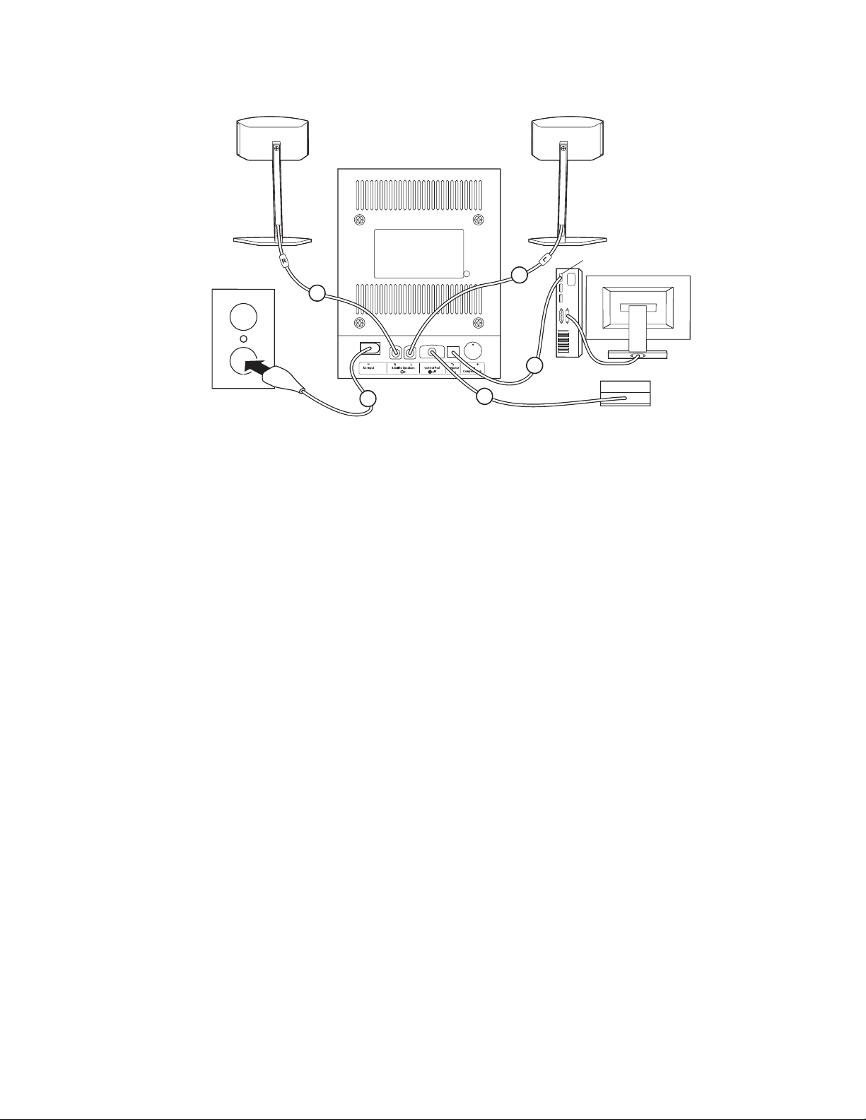
Right (R) speaker
ran ç ais
Left (L) speaker
Acoustimass rear panel
1
1
4
3
2
spaño
Computer USB
Control pod
Overview
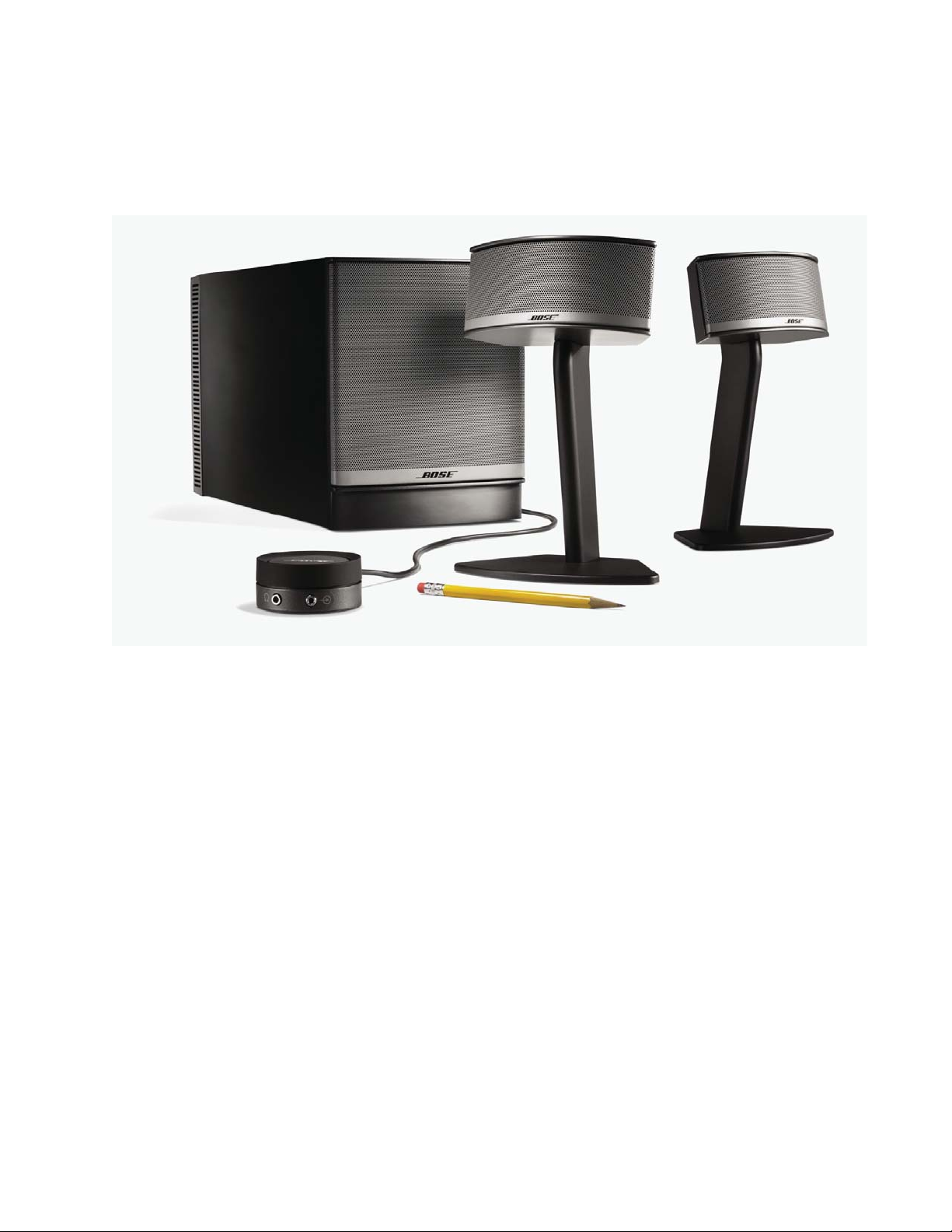
Companion 5 is a multi-channel multimedia speaker system connecting to personal computers via a
USB 2.0 interface. No sound card is required to enjoy 5.1-channel audio content from the host PC.
The two speaker arrays combined with advanced audio processing algorithms provide a spacious
presentation of stereo content and a compelling experience with multi-channel content. A control
module brings the master volume control, simple touch mute control and jacks for an auxiliary
analog stereo input and headphones.
The Companion 5 system consisting of the following major components:
1. Bass speaker enclosure with Woofer, DSP board, I/O board and system power supply.
2. Control Module with an 8-foot (2.4M) cable.
3. Two two-element speaker arrays with integrated cables, uniquely keyed and identified for
left and right locations.
The Bass speaker enclosure is a ported MDF enclosure including the 5.25-inch dual voice-coil
transducer and line power transformer. Both are installed inside the acoustic volume in such a
manner that they are not serviceable. An electronics enclosure is provided at the back of the MDF
enclosure. The heat sink assembly that includes the DSP/Power Amplifier/Power Supply Printed
Circuit Assembly, aluminum heat sink, thermal compound, thermal interface material, and clamping
bracket are screwed directly to the back wall of the acoustic enclosure. Internal cables connect the
DSP/PA/PS assembly to the transformer secondary and the I/O Printed Circuit Assembly that is
mounted to the plastic rear cover of the speaker.
The control module is not serviceable. Only the interface requirements to the Bass module electronics will be discussed in this document. The speaker arrays are mounted on removable speaker
stands that are engineered to position the speakers at the correct height and angle on either side of
a computer monitor. The transducers contained in the speaker enclosures may be replaced from
the front of the enclosure by removing the metal grill. The grill should not be re-used once removed
due to deformation during the removal process. The integrated cable is not removable. The balance
of this document will concentrate on the electronic assemblies present in the bass
module.
2
Page 3
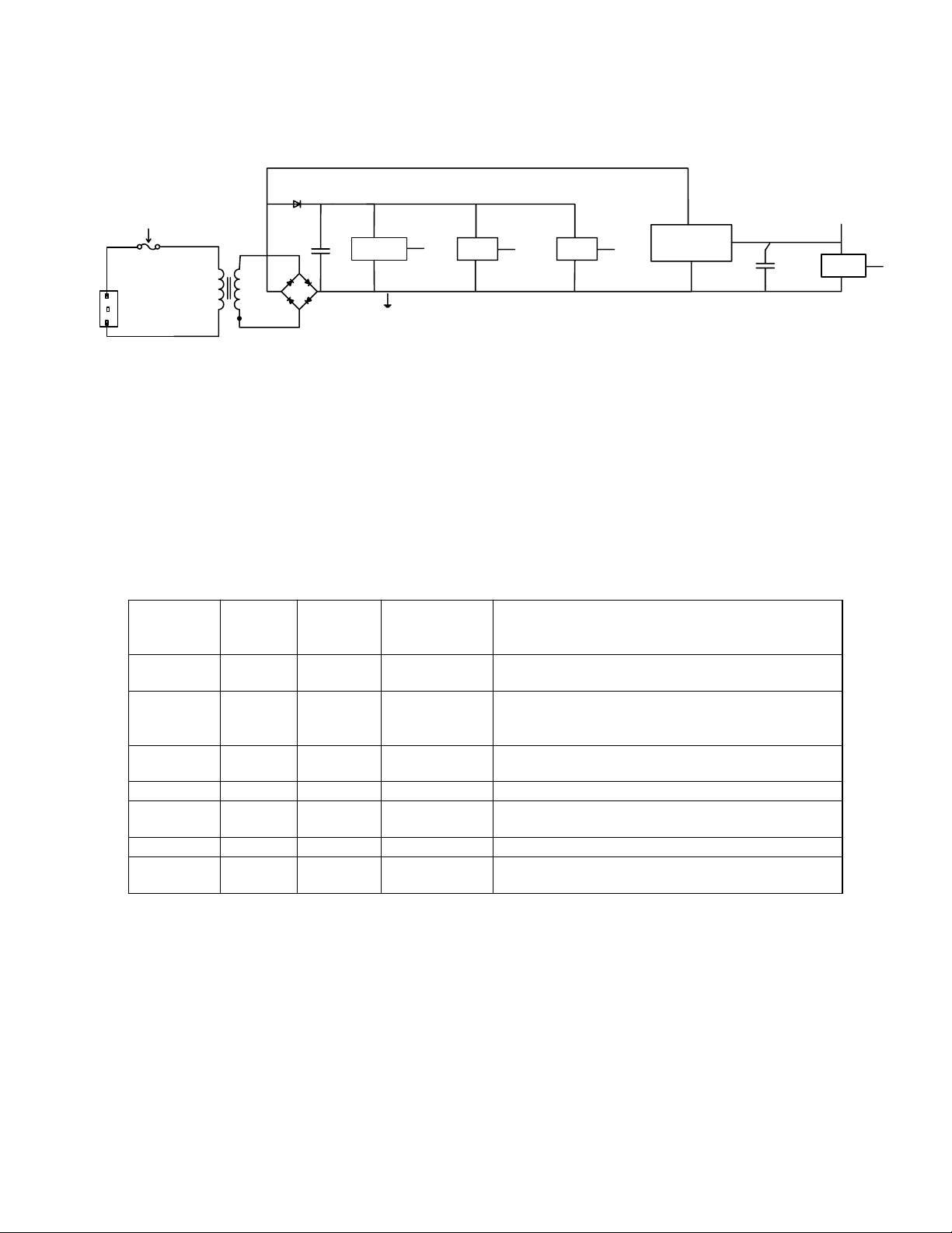
Power Supplies
VSNUB
VRAW
U11
Reg
U902, Q9031
Reg
3.3V
U20
Reg
10V
U50, U51
Reg
1.2V
Q10
Bose Brand FET
Quasi-Regulator
Power Supply Block Diagram
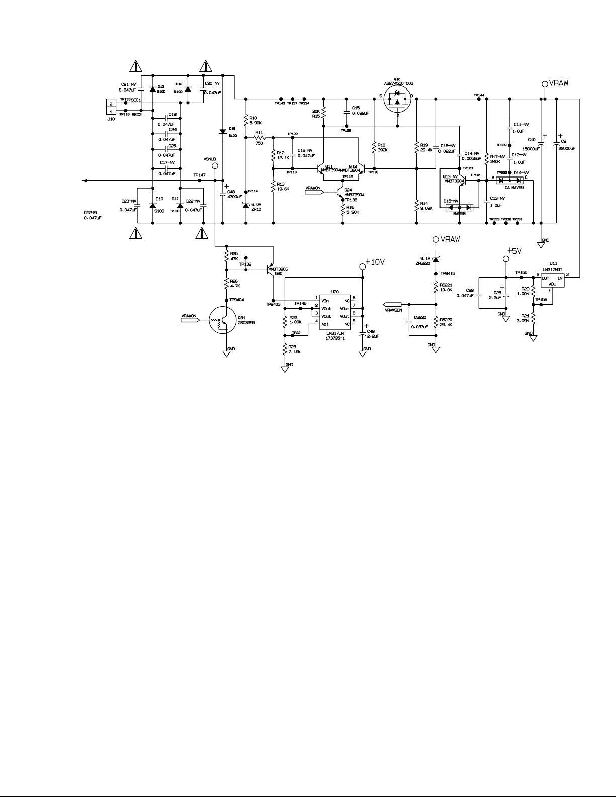
Bass module rectifies un-regulated power VSNUB from the secondary of the line power transformer. VSNUB is,
in turn, converted to the various other potentials required by the system. Nominally 26VDC, this voltage varies
with load and line levels, but is limited to 31.5V maximum(assuming line voltage of 140V AC). This voltage is
present whenever the bass module is plugged into the wall. All the voltage level source are listed in following
table:
5V
Node
Name
Vsnub +26 Full wave
Vraw +14 (no
+10V +10 linear VSNUB Headphone power amplifiers, control module
+5V +5 linear Vraw CODEC Analog power supply
+3.3V +3.3 switching VSNUB DSP I/O power supply, digital supply for USB
+1.2V +1.2 switching VSNUB DSP core power supply.
SENSOR +3.0 series
Output
Voltage
nominal
load)
Type Input from Outputs to
rectifier
pre-
transformer
secondary
VSNUB Power Amplifiers, +5V, VRAWSEN.
Vraw
regulator
output
green LED.
controller, CODEC, EEROM.
+3.3 Switch able supply for control module touch
switch
sensor, control module red LED
3
Page 4
From
T
Transformer
o 3.3 V
Regulator
Power Supply VSNUB
VSNUB
VSNUB is formed by rectifying the transformer secondary potential via power rectifiers D10-D13. An additional
rectifier, D16 prevents discharge of the filter capacitor, C48 through the FET switch, Q10, whenever this switch is
on. For operating conditions other than extremely low line potential, this permits the peak potential at C48 to
track closely to the peak secondary potential. This is substantially higher than the peak potential of the quasiregulated Vraw supply discussed below.
VSNUB also serves as a clamping potential into which some of the energy stored in the leakage reactance of
the mains transformer is discharged when Q10 is switched off. This additionally energy can cause the peak
potential for V-UNREG to actually be greater in magnitude than the peak potential of the transformer secondary
when Vraw current drain is large. VSNUB can range from 20 to 40 volts, depending on input voltage and Vraw
loading.
4
Page 5

From
T
Transformer
o 3.3 V
Regulator
Power Supply VRAW
VRAW
Vraw provided power to the Audio Power Amplifiers, U150, U150, U350, and the +5V regulator. Its potential is
monitored by the DSP, U7000, via the circuit associated with VRAWSEN. When active the potential can vary
from 12 vdc to 14.0 vdc. The circuit controlling the FET switch, Q10, is configured to force commutate (turn off)
the switch whenever the potential of the filter capacitor, either C9 or C10, exceeds the target potential of approximately 13 volts. The nature of the circuit causes Q10 to turn off during high peak currents. These high peak
currents cause a voltage drop on C9’s (C10’s) internal equivalent series resistance (ESR) which, in turn, causes
a drop in the sensed output potential as soon as the switch, Q10 is turned off. In order to prevent the circuit to
immediately turn the switch back on, a fixed voltage hysteresis is applied by the control circuit to lower the turnon threshold of the circuit by 200 to 300 millivolts.
R10 and ZR10 form a 6.0V reference potential for the error amplifier formed by Q11, Q12. R11, R12, and R13
scale this reference voltage to an appropriate potential to permit start-up of the circuit. R11 doubles as the feedback resistor that sets the hysteresis mentioned above. R18 and R19 are essentially in parallel when Q10 is on,
so R18, R19, and R14 set a relatively constant turn-off potential. When Q10 is off, R18 depresses the turn-on
threshold of the circuit proportional to the open-circuit potential of the transformer secondary. This is in addition
to the hysteresis provided by R11 and serves to prevent Q10 from turning on during the highest potentials of the
input mains, as this is when the peak charging currents would be the largest.
Q24 and R16 serve as the enable input and current sink for the error amplifier. Maintaining a constant potential
across R16, causes a constant potential to be applied Gate to Source of Q1 when Q10 is on. C15 controls the
switching speed of Q10, which improves audible and electrical noise characteristics of circuit. Q13 and the
additional components associated with Q13 provide additional shaping of the switching characteristics of Q10
when little power is consumed from Vraw.
5
Page 6
From
T
Transformer
o 3.3 V
Regulator
Power Supply 5V and 10V Regulators
5V
The only internal power requirement for 5 volts are the CODEC, U4000, power supply and the current source for
the ramp circuit formed by Q6201 and R6207. The source for the +5V linear regulator, U11, is Vraw. +5V is
provided only when Vraw is enabled.
10V
This potential is used to power the headphone amplifier and signal that the system is not in stand-by operation.
When installed on the I/O assembly, this potential will drive the primary circuit TRAIC. The GREEN LED on the
control module is driven by this potential. Q30, Q31 and associated components for an enable circuit for the
linear regulator U20. These components permit U20 to be disconnected from Vsnub during stand-by operation,
thus avoiding the quiescent dissipation of U20 during these conditions.
6
Page 7
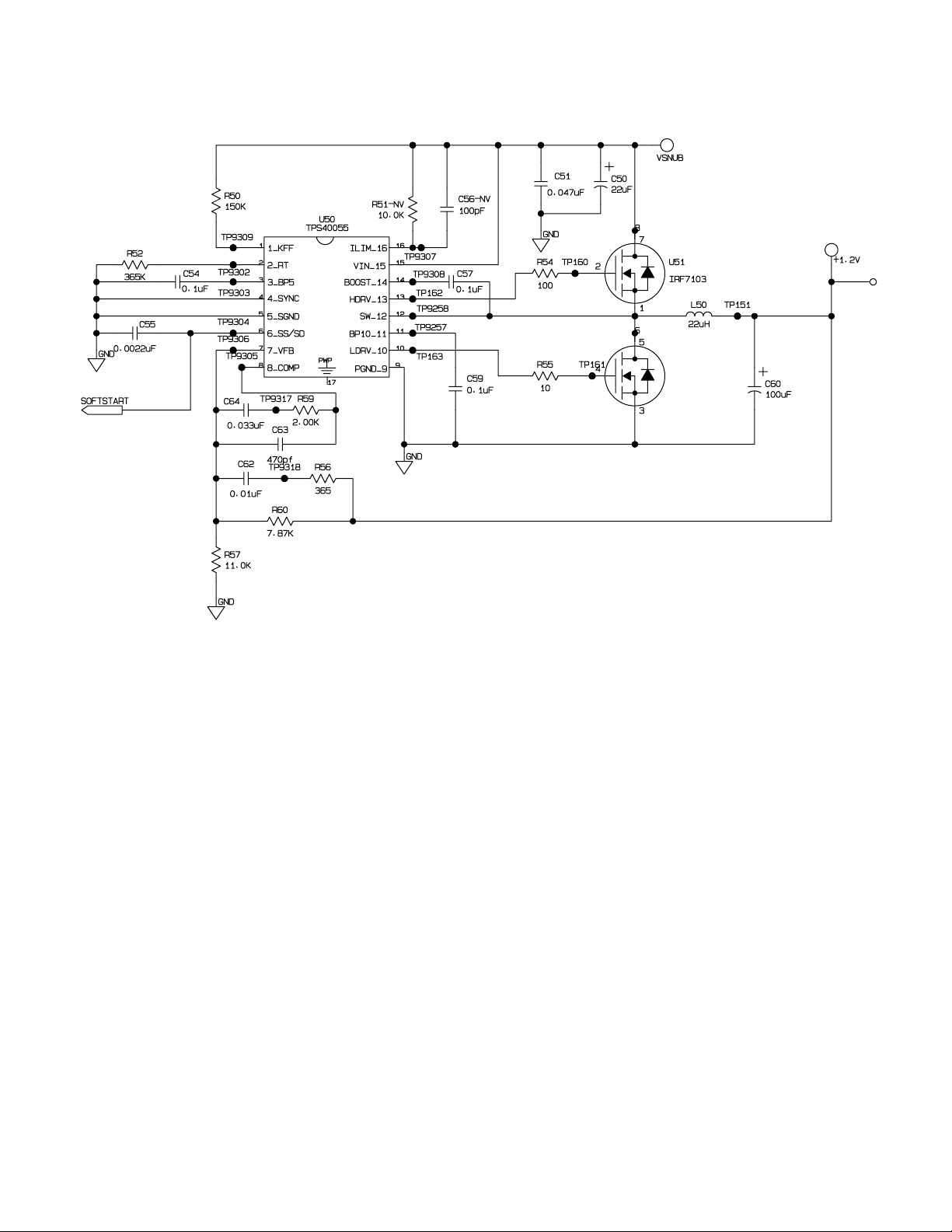
Power Supply 1.2V Regulator
1.2V
The processing core of the DSP is the sole consumer of the 1.2 volt power supply. Its relatively high current
consumption requires efficient power conversion. The Texas Instruments TPS40055, U50, provides the PWM
control functions for a synchronous-rectifier power circuit. U51 is a dual N-channel FET used as switch transistor
and synchronous rectifier for the buck regulator circuit. Inductor L50 and filter capacitor C60 form the filter for the
+1.2V supply. R57 and R60 establish the DC operating voltage for the output. R56, R59, C62, C63 and C64
provide the compensation for the feedback path.
C59 filters the 10 volt reference internal to U50 which is used to control the switching of the transistor drive
signals. C57 provides the boot-strap (boost) potential to drive the high-side switch. C54 filters the 5 volt reference
also generated internally to U50.
R52 sets the operating frequency of the PWM circuit of approximately 100kHz. Resistor R52 provides a
reference to the input voltage which is used by U20 provide feed-forward input voltage compensation. C55
shapes the soft-start characteristics of the regulator.
7
Page 8

Power Supply 3.3V Regulator
3.3V
The USB controller, U6000, the I/O circuitry of the DSP, U7000, and the digital processing portions of the
CODEC, U4000 all require power from +3.3V. This circuitry is biased both during normal operation and stand-by,
so no enable control is required.
U902 is a TI TL5001 switch-mode PWM regulator control circuit. The output is open-collector, and drives the
base of the PNP power transistor, Q9031. Q9032, D9200, R9240, and C9220
provide a boot-strapped circuit to speed the turn-off of Q9031. R9236 and R9237 form a potential divider to
establish the DC operating point of the regulator at +3.3 volts. C9202 provides a lead compensation in the
feedback circuit. R9238 limits the frequency range of the lead compensation.
C9211 is applied around the error amplifier of the TL5001 to create a lag compensation. R9235 limits the frequency range of the lag compensation.
R9232 establishes the approximately 50kHz switching frequency for the PWM generator. C9209 generates a
soft-start ramp when TL5001 starts switching.
8
Page 9

Out to
Control
Pod
Sensor and Power Failure Dectection
USB Controller
Sensor
SENSOR is generated by switching the +3.3 volt supply via Q6102. SENSOR powers the touch sensor in the
control module. switching SENSOR off momentarily forces the control module touch sensor to reset, forcing its
output to the muted state. This is typically performed just prior to entering the stand-by mode of operation. A
subsequent transition from mute to active will cause the system to exit stand-by.
Power Failure Detection
Detection of power failures is accomplished with U6001, a Maxim MAX809 undervoltage detection IC. U6001
directly monitors the +3.3Volt supply which is used by the USB controller, U6000, the DSP I/O circuitry, U7000,
and the CODEC digital circuitry, U4000. In order to prevent an undetected disruption of the DSP due to loss of
the core power supply, the SOFTSTART signal from U50 is used to switch the PNP transistor, Q6000, on
whenever +1.2V has stopped due to undervoltage lockout. Q6000, in turn, removes the +3.3 volts from the
undervoltage detection IC, U6001, forcing a reset of the USB controller.
9
Page 10

USB Controller
USB Controller
USB Controller
The TAS1020B (U6000) micro-controller also serves as the master controller for the system. It manages the
USB interface to the host computer including the enumeration of the system capabilities to the host computer.
U6000 is responsible for managing the status of the USB interface, monitoring the MUTE\ signal from the remote
control, monitoring the status of the audio stream passing through the DSP, and enabling the Vraw, +10V, and
SENSOR power supplies.
USB Controller Oscillator and Clock Generation
All clocks for the system are generated by U6000. Crystal X6000 is driven by U6000 to generate a 6.0MHz
reference clock. This reference is internally multiplied by U6000 to generate its own 48MHz system clock as
well as the internal 24.576MHz master clock for the serial TDM audio path. This internal clock is divided to
produce a 12.288MHz bit clock and a 48kHz frame sync clock for the TDM audio path described later in this
document. A separate 24.576MHz clock is provided for driving the DSP. In order minimize jitter on the output of
the phase-locked loop, a filter for the PLL power supply is created with the components R6009, C61, and C6001.
The PLL dynamics are controlled by the compensation components C6002, C6003, and R6000.
USB Interface
The tolerance of the impedance into which the USB data signals D+, D- must be terminated is relatively tight.
Components R8001, R8001, C8000 and C8001 provide the proper matching to the internal impedance of the data
transmitters of U6000. R8002 provides the necessary pull up to the D+ line in order to signal to the host that the
Companion 5 is present and is a full-speed device. The resistor divider R6011 and R6013 permits U6000 to
sense the presence of the USB5V signal from the host. U6000 is required to remove the signal to R8002
whenever USB5V is not detected.
The signals BADDATA at U6000.31 and USBINT\ at U6000.30 are used to transmit key USB status information
to the DSP controller. When the USB link to the host computer is performing normally, no activity is present on
these signals.
10
Page 11

USB Controller
USB Controller
DSP
Memory and I2C interface
The TAS1020 contains an internal ROM and all Data and Program RAM. An external EEROM, U6002, stores the
portion of the program code custom to the Companion 5 application. Once the TAS1020 has come out of reset,
it will read the code stored in U6002 via the Inter Integrated Circuit (I2C) communications path on pins 43 and
44. This buss is also used for transferring non-audio information between the USB controller and the DSP. The
TAS1020 is permanent master on this buss and provides the clock and command/address portions of all
instructions. The DSP always behaves as the slave device on this interface.
Booting, EEROM
The logic state of pins U7000.[108,110,111] are selected to permit booting from the external EEROM, U7001,
using the I2C protocol. The proper state of pins 108 and 111 depend on the I2C pins of U6000 being idle when
DSPRESET\ is released. The DSP will take approximately 2.8 seconds to read the EEROM contents and
complete internal initialization. In order to assure that the I2C state machine internal to the EEROM, U7001, is
in a known state, the components C7100, Q7100, and R7100 are used to momentarily remove the +3.3V
power from the EEROM each time the USB controller places the DSP into reset.
11
Page 12

D-
D+
5V
REMOTE
TOUCH
SENSO
USB Input
R
Volume
MUTE
6
U6000
7
USB Controller and
Microprocessor
25
Audio clock
master
TAS1020B
3.3V
26
Q6101
Audio Interface
38
113
EEPROM
U7000
TMS320DA71
115
I2C Bus
TI DSP
116
0
120
3.3V 1.2V
McASPs
Audio clock
119
Q6202
Q6203
135
131
134
5V 3.3V
122
126
slave
CCLIP
BSCLIP
Thermistor
RT6307
Thermistor
RT6206
9
ADCs
WM8772 or AK4626
U4000
CODEC
6
DACs
Audio clock
27
28
25
23
26
24
slave
Out to
Amplifier
EEPROM
I2C Bus
31
BADDATA
30
DSPINT
RAMP
GENERATO
VRAW
Bass Knob
138
127
R
n
Aux I
Headphone
U1000
Audio Path
Audio interface
Time Division Multiplexing (TDM) is used to transfer audio data among the USB controller (U6000), DSP (U7000)
and CODEC (U4000). The USB controller is the clock master for the TDM paths. Only one clock domain exists
for exchange of audio information. The USB controller is responsible for synchronizing the local TDM data rate
with the data rate from the USB host, when the host is active. When no host is connected, or when the connected host is suspended, the USB controller is responsible to provide the clocks for the TDM paths at a
nominal 48kHz audio sample rate. No audio data is transferred to the host computer. Additional details of the
TDM audio paths are described later in this document.
U6000.35 sources the frame clock for the TDM paths.
U6000.37 sources the bit clock.
U6000.38 sources the USB audio data received from the USB host.
Serial Interface
The components to support a Boselink hardware compatible serial interface are not installed.
12
Page 13

Miscellaneous Control
USB Controller
To Power
Supply
To DSP
Pin 14
To I/O Board
Miscellaneous Control
Power management is affected by controlling the pins for SENSOR, VRAWON, and DSPRESET\.
SENSOR is controlled by U6000.26, which is inverted in logic level from SENSOR. The function of SENSOR is
explained in section 2.7.
The signal VRAWON (U6000.42 enables both the pre-regulator circuit for Vraw and the +10V power supply as
explained in sections 2.1 and 2.2, respectively. VRAWON is active when the USB controller is held in reset. The
USB controller must complete the boot cycle, enable the DSP controller to boot, and monitor the USB interface
and AUX input signal amplitudes. Only if the USB interface is not active (suspended or disconnected) and if the
signal level of the AUX input is less than -70dB and both conditions have persisted for at least 2 minutes, will the
system be placed into stand-by and VRAWON driven low.
DSPRESET\ is an active low signal driven by pin 41 of U6000. This pin is active low at initial application of power
to U6000, keeping the DSP in reset until U6000 has completed initialization. The signal is then negated (high).
The USB controller will reset the DSP just prior to entering stand-by mode of operation.
Transistor Q6101 inverts the MUTE\ signal from the control module to buffer and generate the MUTE signal to
the USB controller (U6000.26). If the mute signal is not present shortly after the USB controller is initialized, the
controller must assume that the control module is not present and command the DSP to enable the speakers,
speaker EQ and set the system volume to full. At any time the mute signal is present the USB controller
commands the DSP to mute the speaker EQ, mute the speaker Power Amplifiers, and ramp in the headphone
(flat) EQ.
13
Page 14

USB Controller
Digital Signal Processor
DSP
To DSP
Pin 14
DSP
The Texas Instruments TMS320DA705 (U7000) is a floating-point Digital Signal Processor with internal ROM and
192kbytes of internal RAM. No external RAM is required or supported by this processor. The internal ROM
includes a boot loader algorithm that permits booting the custom application portion of the program code from a
variety of external devices. All audio processing, limiting, volume control, bass compensation, monitoring of the
thermal sensors, clip detection, transducer DC offset protection, ETAP command processing and response
generation are performed by the DSP.
DSP Clock
The 24.576MHz DSP clock is provided by U6000. The clock is applied prior to U6000 releasing the DSPRESET\
line.
DSP Reset
Reset for U7000 is controlled solely by the USB controller (U6000) through the DSPRESET\ signal applied to
U7000.14. The DSP is held in reset after power is applied until the USB controller has initialized its operation.
The DSP is also placed into reset by the USB controller just prior to its entering the stand-by operation mode.
14
Page 15

Conversion and Ramp Generation
Analog inputs
Several signals monitored by the DSP are analog in nature. One of the two Advanced Serial Processor (McASP)
engines that are available in the DSP is used to perform the analog to digital conversion with the aid of several
external components.
Conversion Cycle and Ramp Generation
McASP0 is configured as a TDM path with 6 slots of 32 bits/slot. An internally generated bit clock is set at
96kHz. The DSP generates a frame sync pulse (DISCHG) that is high for the duration of the first of the six slots.
The high level on DISCHG causes Q6200 to discharge the capacitor, C6201, to nearly zero volts. During the next
5 slots, or160 bits, Q6200 is turned off and the current source consisting of Q6201 and R6207 charges the
capacitor at a constant rate. The capacitor potential should cross 3.3 volts after 1.33 milliseconds but before
1.67 milliseconds, at which time it will again be discharged by DISCHG pulse.
Signal Conversion
The ramping voltage waveform generated on C6201 is compared to each of the analog signals by independent
comparators, all part of U6200. The logical output of each comparator is routed to a serial input on McASP0.
The serial inputs are programmed to clock in all data present in the 2nd through 6th slots, or last 160 bits of the
TDM frame. At the end of each frame, the buffer associated with each input is scanned to find the location of the
first high-to-low transition of the data. The ratio of the number of bits from the start of the 2nd frame to this
location to the number of bits to the ramp exceeding 3.3 volts is the converted value for each input.
15
Page 16

Ramp Calibration
Ramp Calibration
In order to calibrate the Analog to Digital Conversion, the DSP uses a general-purpose i/o pin to overdrive the
analog VRAWSEN signal present at the comparator input U6200.9 for the duration of a conversion cycle. This
forces the input to +3.3 volts. The bit value read for CPVRAW (U6000.14) becomes the full-scale value. Dividing
this value into the counts obtained on the other inputs, or on future counts obtained on the CPVRAW input
normalizes the counts relative to full scale. This calibration cycle is performed at a regular interval and can be
observed by looking at the VRAWSEN signal. Under normal input line conditions, VRAWSEN will be significantly below 3.3 volts except for the calibration cycle, when it will step to 3.3 volts for the duration of the cycle.
Analog
Signal
BEQ+ CPBCP- 113
BEQ- CPBCP+ 115
Converted
Signal
DSP (U7000)
input pin
Use
Bass compensation. Wiper position can
be determined by (BEQ+ - BEQ-)/(BEQ+
+ BEQ-).
IVOL CPVOL 116 Volume control input when the control
module is present
VRAWSEN CPVRAW 117 Use to prevent clipping of power
amplifiers, monitored to determine
excess energy consumption for
transducer DC offset protection.
16
Page 17

D-
D+
5V
REMOTE
TOUCH
SENSO
USB Input
R
Volume
MUTE
6
U6000
7
TAS1020B
USB Controller and
Microprocessor
25
Audio clock
master
3.3V
26
Q6101
Audio Path
38
EEPROM
I2C Bus
31
BADDATA
30
VRAW
Bass Knob
DSPINT
GENERATO
RAMP
138
127
R
EEPROM
113
I2C Bus
U7000
TI DSP
TMS320DA71
115
116
0
120
3.3V 1.2V
McASPs
Audio clock
119
Q6203
135
131
134
122
126
slave
Q6202
CCLIP
BSCLIP
Thermistor
RT6307
Thermistor
RT6206
9
DACs
ADCs
U4000
WM8772 or AK4626
CODEC
5V 3.3V
6
Audio clock
slave
27
28
25
23
26
24
Out to
Amplifier
Aux I
n
Headphone
U1000
Audio Path
Audio Path
The audio path is implemented on McASP1 of the DSP. All clocks are generated by the USB controller, U6000.
The DSP expects audio input from the USB controller on pin U7000.135. The audio input from the CODEC is
expected on U7000.134. The DSP sends audio data to the CODE on pin U7000.131. All other details of the
audio path will be deferred until section 5. The left and right channels of the USB input are summed with the left
and right channels of the AUX input prior to processing the audio stream. The volume control is applied to the
mixed stream. Volume matching the two streams is accomplished by either using the Windows or application
volume control on the connected PC, or by using the volume control available on the device connected the AUX
input.
Miscellaneous I/O
The DSP receives warning of a USB audio data checksum error on the BADDATA input, U7000.138. USBINT\ is
used to signal other errors. It is present on pin U7000.127.The Power Amplifier Clip Detect output are monitored
by the signals CCLIP\ and BSCLIP\ signals on U7000.122 and 126 respectively. The temperature of the DSP
assembly is monitored by the thermistors RT6206 and RT6307. RT6206 is located between power FET Q10 and
rectifier D10, while RT6307 is located near rectifiers D11 and D12. The thermistors are of the positive temperature coefficient type (PTC) with a nominal resistance of 470 Ohms at 25oC. The resistance of these components
rapidly increases when the temperature is near 105oC. The increase in resistance will increase the base-emitter
voltage on the transistors Q6202 and Q6203 to the point that the transistors will switch to an on state, driving
the DSP inputs U7000.119 and U7000.120 low. When either of these inputs is low, the DSP will reduce the audio
output level by 0.05dB/second for up to 120 seconds. The maximum attenuation is 6dB. When both U7000.119
and U7000.120 are high, the attenuation will be reduced at the same rate until full audio output is again
achieved.
17
Page 18

D-
D+
5V
REMOTE
TOUCH
SENSO
USB Input
R
Volume
Aux I
Headphone
MUTE
n
6
U6000
7
USB Controller and
Microprocessor
25
Audio clock
master
TAS1020B
26
Q6101
3.3V
Audio Path (continued)
38
EEPROM
I2C Bus
31
BADDATA
30
DSPINT
RAMP
R
GENERATO
VRAW
Bass Knob
U1000
EEPROM
3.3V 1.2V
I2C Bus
138
127
U7000
TI DSP
TMS320DA71
113
115
116
135
McASPs
131
134
122
0
126
Audio clock
slave
119
120
Q6202
Q6203
CCLIP
BSCLIP
Thermistor
RT6307
Thermistor
RT6206
WM8772 or AK4626
9
ADCs
U4000
CODEC
DACs
5V 3.3V
6
Audio clock
slave
27
28
25
23
26
24
Out to
Amplifier
Audio Path
CODEC
The Codec, U4000, is an AKM4626A. It features the ability to be either hardwired or serial interface configurable.
For this application, it is configured by hardwiring the pins.
Stand-by Operation
DSPRESET\ is used to power down some of the internal functions of the CODEC in order to conserve power
during stand-by operation. The CODEC is active at all other times
CODEC Audio Inputs and Outputs
The DSP receives warning of a USB audio data checksum error on the BADDATA input, U7000.138. All other
connections to the USB controller and DSP are to implement the TDM audio path.
Six channels of audio output are provided by the CODEC. These six outputs are filtered to remove out-of-band
noise and attenuated 7.5dB to reduce the overall gain of the system and AC coupled to the six power amplifiers
in IC’s U150, U250, and U350. The outputs are single-ended biased to approximately 2.5 volts. The maximum
amplitude for a full-scale digital input signal is approximately 1 volt rms. Of the six channels output by the
CODEC, only five are wired to the Amplifiers. The DAC_BASS1 channel (U4000.23) is used to drive both bass
amplifiers. DAC_LC (U4000.27) and DAC_RC (U4000.28) are also used to drive the headphone amplifiers
(U1000).
Aux Audio Input
The AUX stereo input from the control module is attenuated by -4.3dB. This prevents a
2.0Vrms sine wave input signal from clipping the ADC input, whose max input is 1.0 to 1.1 volts
rms. The converted stereo signal is transmitted to the DSP over the TDM path described in the
next section.
18
Page 19

U6000
TAS1020
Controller
Audio Path (continued)
USB
U4000
AK4626A
CODEC
ADC
TDMA in
TDMA out
DAC
X3
U7000
TM320DA705
DSP
Companion 5 Audio Path
Signal Routing and Clocking
TDM Configuration
As mentioned section 2, the USB controller generates the two clocks required for transmitting the audio stream
via Time-Division Multiplex serial transmission. This is a scheme where all data between two points can be
transmitted over one data line. In Companion 5, separate data lines are used for different paths.
ANALOG STEREO
USB
TDMA, 8 slot: U6000 Provides Clock, Frame Sync
AUX IN
BASS1/BASS2
LS/RS
LC/RC
NJM3414A
BUFFER
U9100
TO
POWER
AMP
HEADPHONE
OUTPUT
The frame sync, FCLK, is generated by the USB controller (U6000.35). This signal is high for the first bit (MSB)
of the first audio sample transmitted in each frame. The frame rate is set at 48kHz. Each of up to six audio
samples is transmitted in sequence followed by two null samples. Each audio sample is left-justified in a field of
32 bits. The eight total samples of 32 bits require a bit clock of 256 times the FCLK or 12.288MHz. This clock,
BCLK, is generated on pin U6000.37.
AUX Audio Input
The AUX stereo input from the control module is continuously converted and transmitted to the DSP via the TDM
data path, AD_DATA (U4000.9).
Slot Assignments for data from the Codec to the DSP are:
Time Slot Audio Data
1 Left Aux
2 Right Aux
3 Not Used
4 Not Used
5 Not Used
6 Not Used
7 Not Used
8 Not Used
19
Page 20

U6000
TAS1020
Controller
Audio Path (continued)
USB
U4000
AK4626A
CODEC
AUX IN
BASS1/BASS2
LS/RS
LC/RC
NJM3414A
BUFFER
U9100
TO
POWER
AMP
HEADPHONE
OUTPUT
TDMA in
U7000
TM320DA705
DSP
Companion 5 Audio Path
Signal Routing and Clocking
TDMA out
ADC
DAC
X3
ANALOG STEREO
USB
TDMA, 8 slot: U6000 Provides Clock, Frame Sync
USB Audio Input
Audio information from the Personal Computer can contain anywhere from two to six channels of information.
This data is transferred from the USB controller to the DSP on the TDM data line connected to U6000.38
(unnamed on the schematic).
Slot Assignments for data from the USB Controller to the DSP are:
Time Slot Audio Data
1 Left
2 Right
3 Center
4 LFE
5 Left Surround
6 Right Surround
7 Not Used
8 Not Used
DSP audio output
Audio information is transmitted to the CODEC from the DSP on TDM data line DA_DATA1 (U7000.134).
Slot assignments for Audio data from the DSP to the Codec are:
Time Slot Audio Data Muted
1 Left Channel (Inner) Left Headphone
2 Right Channel (Inner) Right Headphone
3 Left Surround (Outer) Don’t Care
4 Right Surround (Outer) Don’t Care
5 Bass Don’t Care
6 Bass Don’t Care
7 Don’t Care Don’t Care
8 Don’t Care Don’t Care
20
Page 21

Power Amplifiers
Power Amplifiers
The Phillips TDA8566 power amplifiers (U150, U250, U350) provide 26dB voltage gain and the capability to drive
speakers with 2 to 4 Ohm DCR. The Equalization for the system requires the amplifiers to drive to approximately
9.5 volts peak. Thus a 450 millivolts peak input is sufficient for the system to generate the peak audio power
required.
The power amplifiers each have an open collector output from their clip detection circuitry that is active whenever
either of the output transistors are saturated. The DSP monitors the status of clip detect for U150.11 via the
CCLIP\ signal. U150 drives the inner (center) transducers of the left and right speaker arrays. U250.11 and
U350.11 are both connected wire-or to the DSP via BSCLIP\. U250 drives the “B” coil of the bass transducer and
the outer (surround) transducer of the right array. U350 drives the “A” coil of the bass transducer and the outer
transducer of the left array.
Mode
The MODE input on pin 20 of the devices mutes the power amplifiers when the potential at the pin is between
3.3 and 6.4 volts. When muted the power amplifiers remain biased and the outputs active. The power amplifiers
are active when the MODE input is above 8.5 volts. If the MODE potential is below 2 volts the amplifiers will be
placed in stand-by. In this condition the internal bias for the amplifiers is turned off and the outputs are not
active. Companion 5 does not use this state. During system stand-by, the Vraw power supply is turned off.
Transistor Q450, resistors, R451 and R453, and Zener D450 convert the MUTE signal from the USB controller to
the proper potential for MODE. When MUTE is high, the level at MODE should be 4.5-6.5 volts
21
Page 22

Left and Right
Audio from
CODEC
Headphone Amplifiers
Out to I/O Board
and Headphone
Jack
Headphone Amplifiers
The amplifiers, U1000, are configured to provide 2.3 dB non-inverting voltage gain in order to drive the headphones. The headphone amplifiers are not capable of being muted. The control module must provide a mute
signal any time the headphones are plugged in. This causes the system to mute the speakers and ramp in the
headphone (flat) EQ required. The outputs of the amplifiers are biased to 3.25 volts due to the 2.3dB gain and
the 2.5 volt bias of the CODEC outputs. The worst case output voltage swing from the codec is 1.6 volts. Thus
with the gain of the amplifier circuit will cause the worst case output voltage from the headphone amplifiers to
from 1.15 to 5.35 volts, or 4.2 volts peak-to-peak.
The bias potential present at the output of the headphone amplifiers is removed from the headphone signals by
C1008 and C1008. The signals at the cathodes of these capacitors will be balanced around the GND reference.
The signal RMTRET present at both the AUX input components and the headphone amplifier circuits is a
dedicated ground trace to the remote control module that is terminated to GND near the codec. This prevents
noise due to power supply currents circulating in GND from coupling to either the AUX inputs or the headphone
22
Page 23

Block Diagram
Bass
Left
U150
9
8
Filter
27
DACs
ADCs
Right
16
Amplier
TDA8566
18
2
Surround
161813
U350
3
3
2
Filter
Filter
25
28
U4000
WM8772 or AK4626
CODEC
TDA8566
8
Amplier
9
Filter
23
Right
Surround
13
15
18
16
15
Audio Path
Amplier
TDA8566
U250
3
2
9
8
Filter
Filter
24
26
slave
Audio clock
RT6307
RT6206
Thermistor
Thermistor
Left
13
VRAW
5V 3.3V
15
6
9
Companion 5 Block Diagram
5V
TITLE
Reg
U11
VRAW
Q10
Quasi-Regulator
Bose Brand FET
1.2V
Reg
U50, U51
VSNUB
10V
Reg
U20
3.3V
Reg
U902, Q9031
134
131
EEPROM
135
McASPs
3.3V 1.2V
0
I2C Bus
TI DSP
U7000
TMS320DA71
slave
Audio clock
119
Q6202
Q6203
120
116
115
113
117
R
I2C Bus
EEPROM
RAMP
GENERATO
VRAW
Bass Knob
U1000
38
3.3V
TAS1020B
U6000
Microprocessor
USB Controller and
25
7
6
master
Audio clock
26
Q6101
USB Input
MUTE
R
TOUCH
SENSO
REMOTE
D-
5V
D+
n
Aux I
Volume
Headphone
23
 Loading...