


M7VKE
Federal Communications Commission
(F.C.C) Statement
T his device complies with Part 15 of the FCC Rules. Operation of this
device is subjec t to the following two conditions: (1 ) this device may not
cause harmful interference, and (2) this device must accept any
interference received, including interference that may cause undesired
operation.
Acce ssories: This devi ce has been tested and found to comply with the
limits of a Class B digital device, the accessories associated with this
equipment are as follows:
1. Shielded serial cable. (Can be obtained from multiple retail outlets)
2. Shielded printer cable. (Can be obtained from multiple retail outlets)
3. Shielded video cable. (Can be obtained from multiple retail outlets)
4. Shielded power cord. (Provided by manufacturer)
These accessories are required to ensure compliance with FCC Rules. It
is the responsibility of the user to provide and use these accessories
properly.
This equipment has been tested and found to comply with the limits of a
Class B digital device, pursuant to Part 15 of the FCC Rules. These limits
are designed to provide reasonable protection against harmful interference
in a residential installation. This equipment generates, uses and can
radiate radio frequency energy and, if not installed and used in accordance
with the instructions, may cause harmful interference to radio
communications. There is no guarantee that interference will not occur in
a particular installation. If this equipment does cause harmful interference
to radio or television reception, which can be determined by turning the
equipment off and on, you are encouraged to try to correct the
interference by one or more of the following measu res:
1. Reorient / relocate the receiving antenna.
2. Increase the separation between the equipment and receiver.

3. Connect the equipment into an outlet on a circuit different from that
to which the receiver is connected.
4. Consult the dealer or an experienced radio/TV technician for help.
Caution: Changes or modifications not expressly approved by the
manufacturer could void the user’s authority to operate the equipment.
Disclaimer
The vendor makes no repr esentations or warranties with resp ect to the
contents here of and specially disclaims any implied warranties of
merchantability or fitness for any purpose. Further the vendor reserves the
right to revise this publication and to make changes to the content s here of
without obligation to notify any party beforehand.
Duplication of this pub licat ion, in par t or in whole, is no t allowed without
first obtaining the vendor’s approval in writing.
Trademarks and Remarks
MS-DOS, Windows NT, Windows 9X, Windows 2000 and Windows
ME are products of Microsoft Corp, with its ownership of trademark, and
are distributed by the vendor under a license agreement.
All trademarks used in this manual are the property of their respective
owners.
Copyright© 2001
All Rights Res e r v e d
Canadian D.O.C. Statement
This digital apparatus does not exceed the Class B limits for radio noise
emissions from digital apparatus as set out in the radio interference regulations of
the Canadian Department of Communications.
Cet appareil numbérique n‘émet pas de bruits radioélectriques dépassant les
limites appliquées aux appareils numbériques de Class B préscrits dans le
réglement du brouillage radioélect riq u e edict par le mini ster Des Communication s
du Canada.

Contents
i
Introduction ................................................................................1-1
1. Motherboard Description .............. ........................................1-2
1.1 Features...................................................................................................1-2
1.1.1 Hardware.........................................................................................1-2
1.1.2 Software ..........................................................................................1-5
1.1.3 Attachments.....................................................................................1-5
1.2 Motherboard Installation.........................................................................1-6
1.2.1 Layout of Motherboard ...................................................................1-6
1.3 Motherboard Quick Reference................................................................1-7
1.3.1 Front Panel Connectors (JPANEL1 / JPANEL2)............................1-8
1.3.2 Floppy Disk Connector (FDD1)....................................................1-10
1.3.3 Hard Disk Connectors (IDE1/IDE2) .............................................1-10
1.3.4 ATX 20-pin Power Connector (JATXPWR1)...............................1-11
1.4 Back Panel Connectors .........................................................................1-12
1.4.1 PS/2 Mouse / Keyboard CONN.: JKBMS1 ..................................1-12
1.4.2 USB Connectors: JUSB1 ..............................................................1-13
1.5 Serial and Parallel Interface Ports... ... .................. .. .. .................. ... .. ......1-16
1.6 CPU Installation....................................................................................1-19
1.7 Jumper Settings.....................................................................................1-20
1.7.1 CPU Fan Connector: JCFAN1 ......................................................1-21
1.7.2 System Fan Connector: JSFAN1 ...................................................1-21
1.7.3 System Fan Connector: JSFAN3 (Optional) .................................1-21

Contents
ii
1.7.4 Wake-On MODEM Connector: JWOM1 (Optional) ....................1-21
1.7.5 Wake-On-LAN Connector: JWOL1..............................................1-22
1.7.6 CMOS Function Selection: JCMOS1............................................1-22
1.8 DRAM Installation................................................................................1-23
1.8.1 DIMM ...........................................................................................1-23
1.8.2 How to install a DIMM Module....................................................1-24
1.9 Audio Subsystem...................................................................................1-25
1.9.1 CD Audio-In Connectors: JCDIN1/JCDIN2 .................................1-26
1.9.2 Telephony Connector: JTAD1 ......................................................1-26
1.9.3 AUX Audio in Connector: JAUX1 (Optional)..............................1-26
1.9.4 Front Audio Connector: JF_AUDIO (Optional)............................1-27
2. BIOS Setup.............. ... ..................... ... ..................... ... .............2-1
2.1 Main Menu..............................................................................................2-3
2.2 Standard CMOS Features........................................................................2-5
2.3 Advanced BIOS Features........................................................................2-8
2.4 Advanced Chipset Features...................................................................2-12
2.5 Integrated Peripherals ...........................................................................2-17
2.6 Power Management Setup.....................................................................2-22
2.7 PnP/PCI Configurations........................................................................2-27
2.8 PC Health Status ...................................................................................2-30
2.9 Frequency/Voltage Control...................................................................2-31
2.10 Load Fail-Safe Defaults ......................................................................2-32
2.11 Load Optimized Defaults....................................................................2-33

Contents
iii
2.12 Set Supervisor / User Password ....... .. .. ................ .. ................ .. ... ........ 2 -34
2.13 Save & Exit Setup ...............................................................................2-36
2.14 Exit Without Saving............................................................................2-37
3. Software Setup........... .......................................... ... ................3-1
3.1 Software List...........................................................................................3-1
3.2 Software Installation ...............................................................................3-2
3.3 Using Software........................................................................................3-4
4. Trouble Shooting ................... ..................... ... ..................... ... .4-1

Chapter 1 Motherboard Description
1-1
Introduction
System Overview
Thanks for buying this pro duct! This manual was written to help you star t u s in g this
product as quickly and smoothly as possible. Inside you will find adequate
explanations t o solve most problems. In order for t his reference material t o be of
greatest use, refer to the “expan d ed tab l e of con te n ts” to find relevant topics.
This board in corporates the system board, I /O, and PCI IDE int o one board that
provides a total PC solution. The mainboard, a AMD Athlon
TM
and Duron
TM
processor based P C Micro ATX system, support s single proc essors with P CI Local
Bus, and AGP Bus to support upgrades to your system performance. It is ideal for
multi-tasking and fully suppor ts MS-DOS, Windows, Windows NT, W indows 2000,
Novell, OS/2, Windows95/98, Windows ME, UNIX, SCO UNIX etc. This manual
also explains how to install the mainboard for operation, and how to setup your
CMOS configuration with the BIOS setup program.

Chapter 1 Motherboard Description
1-2
1. Motherboard Description
1.1 Features
1.1.1 Hardware
CPU
− Single AMD Socket-A for Athlon
TM
(Thunderbird
TM
) / Duron
TM
processor Module-500MHz and faster.
− 200MHz System Interface speed.
Speed
− Support 33MHz PCI Bus speed.
− Support 4X AGP Bus.
DRAM Memory
− Supports 8/16/32/64.......MB DIMM module socket.
− Supports Synchronous DRAM (3.3V).
− Support a maximum memory size of 1024MB with SDRAM.
Shadow RAM
− A memory controller provide shadow RAM and supports 8-bit ROM
BIOS.
Green Function
− Support power management ope ration via BIOS.
− Power down timer from 1 to 15 mins.
− Wakes from power saving sleep mode at the press of any key or any
mouse activity.
BUS Slots
− Provide one AG P slot.
− Three 32-bit PCI bus master slots.
− Provides CNR (Modem function only) slot . The CNR slot only support
the secondary codec on the CNR slot.

Chapter 1 Motherboard Description
1-3
Flash Memory
− Supports flash memory.
− Supports ESCD Function.
IDE Buil t - in On Boa rd
− Supports four IDE hard disk drives.
− Supports PIO Mode 4, Master Mode, high performance hard disk drives.
− Supports Ultra DMA 33/ 66/ 100 Bus Master Mode.
− Supports IDE interface with CD-ROM.
− Supports high capacity hard disk drives.
− Supports LBA mode.
Stereo AC 97 Digital Audio Codec
− AC 97 2.1 interface.
− 16 channels of high-quality sample rate conversion.
− 16x8 channel digital mixer.
− Stereo 10 band grap h ic equalizer.
− Sound Blaster® and Sound Blaster Pro® emulation.
− 64-voice wavetable.
− PC99 complaint and WHQL certified.
I/O Built-in On Board
− Supports one multi-mode Parallel Port.
(1) Standard & Bidirection Parallel Port.
(2) Enhanced Parallel Port (EPP).
(3) Extended Capabilities Port (ECP).
− Supports two serial ports, 16550 UART .
− Supports one Infra red transmission (IR).
− Supports PS/2 mouse and PS/2 keyboard.
− Supports 360KB, 720KB, 1.2MB, 1.44MB, and 2.88MB floppy disk
drivers.

Chapter 1 Motherboard Description
1-4
Universal Serial Bus
− Supports two back Universal Serial Bus (U.S.B.) Ports and two front
Universal serial Bus (U.S.B) Ports (Optional).
− Supports 48 MHz USB.
Hardware Monitor Function
− CPU Fan Speed Monitor.
− System (Optional) and CPU Temperature Monit o r.
− System Voltage Monitor.
Dimensions (Micro ATX)
− 22.2 cm X 24.3 cm (W x L)
Integrated Savage4 2D/3D/Video Accelerator
− Optimized Shared Memory Architecture (SMA).
− 2 to 32 MB frame buffer using system memory.
− Floating point tria ngle setup engine .
− Single cycle 128-bit 3D architecture.
− 8M triangles/second setup engine.
− 140M pixels/second trilinear fill rate.
− Full AGP 4x, including sideband addressing and execute mode.
− S3 DX6 texture com pression (S3TC).
− Next generation, 128-bit 2D graphic s engine.
− High quality DVD video playback.
− Flat panel monitor support.
− 2D/3D resolutions up to 1920x1440.

Chapter 1 Motherboard Description
1-5
1.1.2 Software
BIOS
− AWARD legal BIOS.
− Supports APM1.2.
− Supports USB Function.
− Supports ACPI.
Operating System
− Offers the highest performance for MS-DOS, OS/2, Windows NT,
Windows 2000, Windows 95/98, Windows ME, Novell, UNIX, SCO
UNIX etc.
1.1.3 Attachments
− HDD Cable.
− FDD Cable.
− Flash Memory Writer for BIOS Update.
− USB2 Cable (Optional).
− Rear I/O Panel for ATX Case (Option al) .
− Fully Setup Driver CD.

Chapter 1 Motherboard Description
1-6
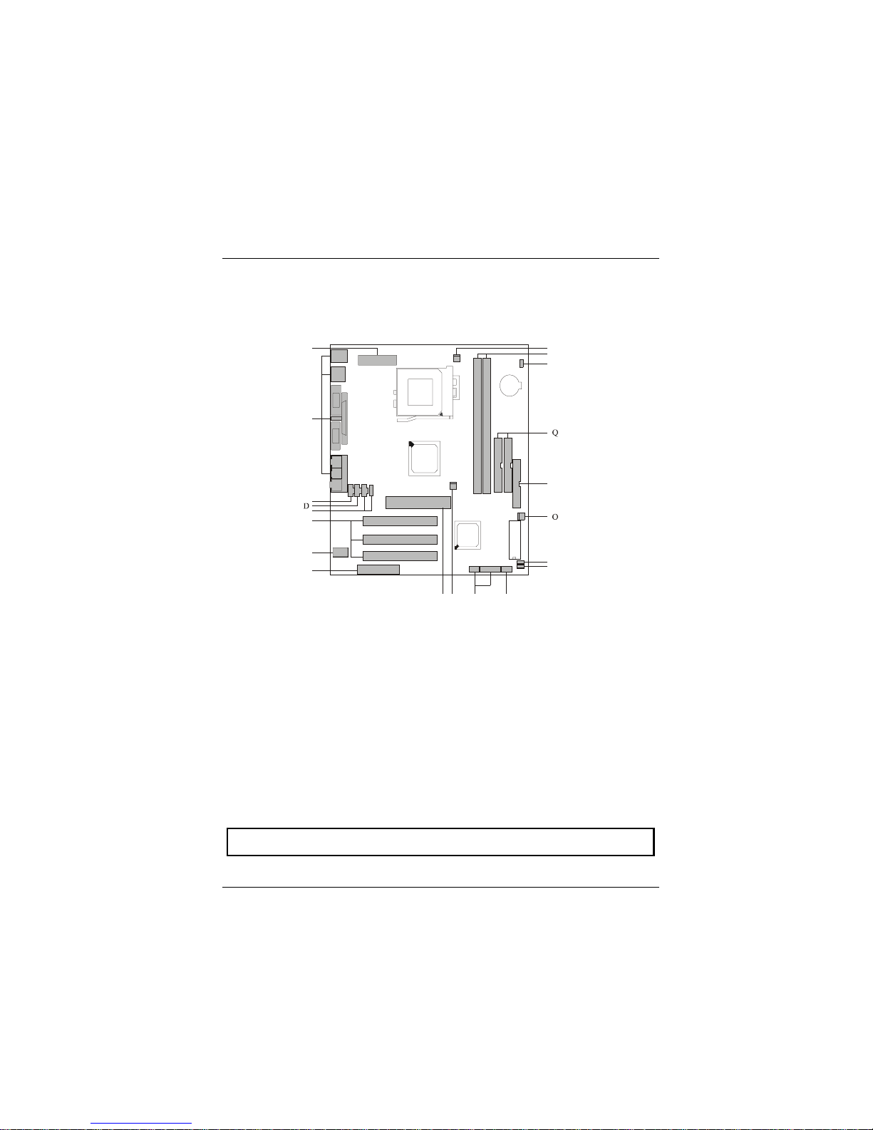
1.2 Motherboard Installation
1.2.1 Layout of Motherboard
Model No.M7VKE
Chapter 1 Motherboard Description
1-7
1.3 Motherboard Quick Reference
A. ATX Power Connector (JATXPWR1) K. Front Panel Connector (JPANEL1-2)
B. Back Panel I/O Connectors L. Front USB Connector (JUSB2)
C. Telephony Connector (JTAD1)
M. Wake-On-LAN Connector (JWOL1)
D. AUX Audio-In Connector (JAUX1*) N. Wake-On MODEM Connector (JWOM1*)
E. CD Audio-In Connector (JCDIN1-2) O. System Fan Connector (JSFAN1)
F. PCI BUS Slots (PCI1-3) P. FDD Connector (FDD1)
G. Front Audio Connector (JF_AUDIO) Q. IDE Connectors (IDE1-2)
H. CNR Slot (CNR1) R. CMOS Function Selection (JCMOS1)
I. AGP BUS Slot (AGP1) S. DIM Ms (DIMM2-3)
J. Chipset Fan Connector (JSFAN3*) T. CPU Fan Connector (JCFAN1)
NOTE: The “ * “mark represent the function is optional.
B
C
E
F
G
H
IJ K L
M
N
P
R
S
T
A
Chapter 1 Motherboard Description
1-8
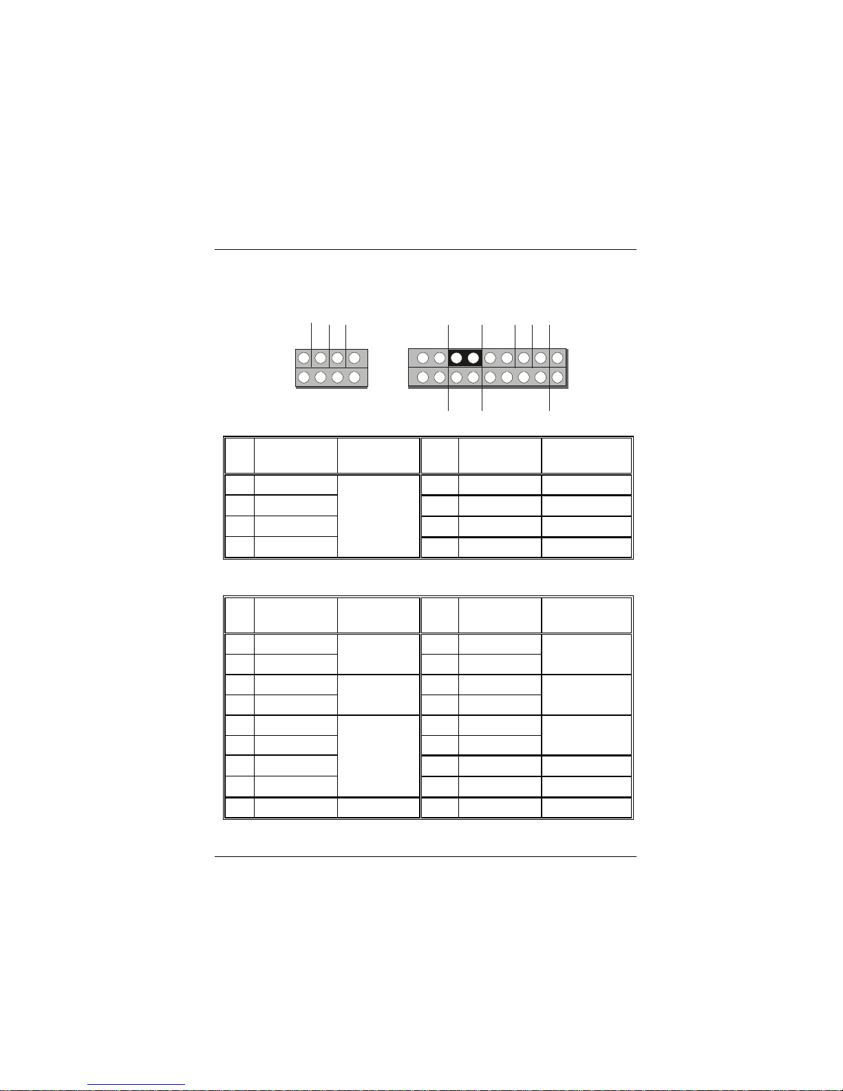
1.3.1 Front Panel Connectors (JPANEL1 / JPANEL2)
JPANEL1
Pin Pin
No.
Assignment Function
No.
Assignment Function
1
+5V
2
+5V VCC
3
No Connection Speaker
4
Ground Ground
5
No Connection Connector
6
No Connection No Connection
7
Speaker 8 Power LED(-) PWR LED
JPANEL2
Pin Pin
No.
Assignment Function
No.
Assignment Function
1
HDD LED (+) Hard Drive
2
Power LED (-)
3
HDD LED (-) LED
4
Power LED (+)
PWR LED
5
Ground Reset 6 Power Button ATX Power
7
Reset Control Button
8
Ground Button
9
+5V
10
Sleep Control
11
Ir-In IrDA
12
Ground
SLP Button
13
Ground Connector
14
No Connection No Connection
15
Ir-Out
16
+5V VCC
17
No Connection No Connection
18
No Connection No Connection
SPK
PWR-LED
RST IRHLED
GV
VSLPPWR
2
1
17
18
NC
NC
NC
NC
17
2
PWR-LED
JPANEL1 JPANEL2
8

Chapter 1 Motherboard Description
1-9
Speaker Connector
An offboard speaker can be install ed o n the motherbo ard as a manufactu ring optio n .
An offboard speaker can be connected to the motherboard at the front panel
connector. The speaker (onboard or offboard) provides error beep code information
during the P ower On Sel f-Test when the computer cann ot use the video interface.
The speaker is not connected to the audio subsystem and does not receive output
from the audio subsystem.
Reset Button
This connecto r can be connected to a momentary SPST type switch that is normally
open. When the switch is closed, the motherboard resets and runs the POST.
Power LED Connector
This connector can be connected to an LED that will light when the computer is
powered on.
Hard Drive LED Connector
This connector can be connected to an LED to provide a visual indicator that data is
being read from or written to a hard drive. For the LED to function properly, an
IDE drive must be connected to the onboard ha rd drive controller.
Infrared Connector
After the IrDA interface is configured , files can be transferred from or to portable
devices such as laptop s, PDAs, and printe rs u sin g ap p l i cation software.
Sleep Button
When APM is enabl ed i n t he system B IOS, a n d th e o pera ting system’s AP M dr iver
is loaded, the system can enter sleep (standby) mode in one of the follo win g ways:
•
Optional front panel SMI button
•
Prolonged system inactivity using the BIOS inactivity timer feature
T
he 2-pin header lo cated on the front panel I/O connector suppo rts a front panel
SMI switch, which must be a momentary SPST type that is normally open.
Closing the SMI switch sends a System Management Interrupt (SMI) to the
processor, which immediately goes into System Management Mode (SMM).While
the computer is i n sleep mode it is fully capable o f responding to and servicing
external inter ru p ts (such as an incoming fax) even tho u gh the monitor tu rn s on only
if a keyboard or mouse interrupt occurs. To reactivate or resume the system, the
SMI switch must be pressed again, or the keyboard or mouse must be used .

Chapter 1 Motherboard Description
1-10
Power On Button
This connector can b e connected to a fron t panel power switch. The switch must
pull the Power Button pin to ground for at least 50 ms to signal the power supply to
switch on or off. (The time requirement is due to internal debounce circuitry on the
motherboard). At least two seconds must pass before the power supply will
recognize another on/off signal.
1.3.2 Floppy Disk Connector (FDD1)
The motherboard provides a standard floppy disk connector (FDC) that supports
360K, 720K, 1.2M, 1.44M and 2.88M floppy disk types. This connector supports
the provided floppy drive ribbon cables.
1.3.3 Hard Disk Connectors (IDE1/IDE2)
The motherboard has a 32-bit Enhanced PCI IDE Controller that provides PIO
Mode 0~4, B us Master, an d Ultra DMA / 3 3, Ultra DM A / 66, Ultra D MA / 100
(optional) functionality. It has two HDD connectors IDE1 (primary) and IDE2
(secondary). You can connect up to four hard disk drives, a CD-ROM, a 120MB
Floppy (reserved for fu ture BIOS) and othe r devices to IDE1 and I DE2. These
connectors support the IDE hard disk cable provided.
•
IDE1 (Primary IDE Connector)
The first hard drive should always be connected to IDE1. IDE1 can connect a
Master and a Slave d rive. You must con figure the second har d drive on IDE1 to
Slave mode by setting the jumper accord ingly.
•
IDE2 (Secondary IDE Connector)
The IDE2 controller can also support a Master and a Slave drive. The configuration
is similar to IDE1. The second drive on this controller must be set to slave mode.

Chapter 1 Motherboard Description
1-11
1.3.4 ATX 20-pin Power Connector (JATXPWR1)
This connector supports the power button on-board. Using the ATX power
supply, funct ions such as Modem Ring Wake-Up and Soft Power Off are supporte d
on this motherboard. This power connector supports instant power-on functionality,
which means that the system will boot up instantly when the power connector is
inserted on the board.
Pin No. Assignment Pin No. Assignm e nt
1 +3.3V 11 +3.3V
2 +3.3V 12 -12V
3 Ground 13 Ground
4 +5V 14 PS_ON
5 Ground 15 Ground
6 +5V 16 Ground
7 Ground 17 Ground
8 PW_OK 18 -5V
9 5V_SB 19 +5V
10 +12V 20 +5V

Chapter 1 Motherboard Description
1-12
1.4 Back Panel Connectors
1.4.1 PS/2 Mouse / Keyboard CONN.: JKBMS1
The motherboard provid es a standard PS/2 mouse / Keybo ard mini DIN conn ector
for attaching a PS/2 mouse. You can plug a PS/2 mouse / Keyboard directly into
this connector. The connector locat io n and pin definition are shown below:
PS/2
Keyboard
PS/2
Mouse
USB
VGA1
Parallel
Game Port
Speaker
out
Line
in
Mic
in
JKBMS1
JUSB1
CN2
COM1
CN1 CN3
U14
Pin 1 KBD DATA
Pin 3 GND
Pin 5 KBD Clock
Keyboard
PS / 2 Mouse
Pin 2 NC
Pin 4 VCC
Pin 6 NC
Pin 2 NC
Pin 4 VCC
Pin 6 NC
Pin 1 Mouse DATA
Pin 3 GND
Pin 5 Mouse Clock

Chapter 1 Motherboard Description
1-13
PS/2 Mouse / Ke yboard Connectors
Pin No. Signal Na me
1 Data
2 No connection
3 Ground
4 +5 V (fused)
5 Clock
6 No connection
1.4.2 USB Connectors: JUSB1
The motherboard provides a OHCI (Open Host Controlle r Interface) Universal
Serial Bus Roots for attaching USB devi ces such as: keyboard, mouse an d other
USB device.
Stacked USB Connectors
Pin No. Assignment
1 +5 V (fused)
2
USBP0- [USBP1-]
3
USBP0+ [USBP1+]
4 Ground
Signal names in brackets (
[]
[][]
[]
) are for USB Port 1.
JUSB1
1432
USB
1432

Chapter 1 Motherboard Description
1-14
1.4.3 Monitor Connectors: JVGA1
This motherboard has built in video facilities. You r monitor will a ttach directly to
JVGA1 connector on th e mot h erb o ard .
Pin
No.
Assignment
Pin
No.
Assignment
1 Red 2 Green
3 Blue 4 +5V
5 Ground 6 Ground
7 Ground 8 Ground
9 +5V 10 Ground
11 +5V 12 DDC/Data
13 HSYNC 14 VSYNC
15 DDC/CLK
JVGA1
1
1115
5

Chapter 1 Motherboard Description
1-15
1.4.4 Front USB Connector: JUSB2
Pin
No.
Signal Name
Pin
No.
Signal Name
1 +5V 2 Ground
3 USBP2- 4 Ground
5 USBP2+ 6 USBP3+
7 Ground 8 USBP3-
9 Ground 10 +5V
JUSB2
10
2
19

Chapter 1 Motherboard Description
1-16
1.5 Serial and Parallel Interface Ports
This system comes equipped wit h one seri al port an d one pa rallel port . Both types
of interface ports will be explained in this chapter.
The Serial Interface: CN1
The serial interface port is sometimes referred to as an RS-232 port or an
asynchronous communication port. Mice, printers, modems and other peripheral
devices can be connected to a serial port. The serial port can also be used to
connect your computer with another computer system. If you wish to transfer t he
contents of your hard disk to anoth er system it can be accomplish ed by using ea ch
machine’s serial port.
The serial port on this system has one 9-pin connector. Some older computer
systems and peripherals used to be equipped with only one 25-pin connector.
Should you need to connec t your 9-pin serial port to an older 25-pin serial port, you
can purchase a 9-to-25 pin adapter.

Chapter 1 Motherboard Description
1-17
Connectivity
The serial port can be used in many ways, and it may be necessary to become
familiar with the pinout diagram. The following chart gives you the function of
each pin on the 9-pin connector and some of the 25-pin connector. This information
can be used when configuring certain software pr ograms to work with the serial
port.
Signal Name DB9 PIN DB25 PIN
DCD Data Carrier Detect 1 8
RX Receive Data 2 3
TX Transmit Data 3 2
DTR Data Terminal Ready 4 20
GND Signal Ground 5 7
DSR Data Set Ready 6 6
RTS Request to Send 7 4
CTS Clear to Send 8 5
RI Ring Indicator 9 22

Chapter 1 Motherboard Description
1-18
Parallel Interface Port : CN2
Unlike the serial port, parallel int erface port ha s been sta ndardized and s hould n ot
present any difficulty interfacing peripherals to your system. Sometimes called
Centronics port, the parallel port is almost exclusively used with printers. The
parallel port on your system has a 25-pin, DB25 connector (see picture b e lo w). The
pinouts for the parallel port are shown in the table below.
Signal Pin
-Strobe 1
Data 0 2
Data 1 3
Data 2 4
Data 3 5
Data 4 6
Data 5 7
Data 6 8
Data 7 9
-Ack 10
Busy 11
Paper Empty 12
+Select 13
-Auto FDXT 14
-Error 15
-Init 16
-SLCTN 17
Ground 18
Ground 19
Ground 20
Ground 21
Ground 22
Ground 23
Ground 24
Ground 25

Chapter 1 Motherboard Description
1-19
1.6 CPU Installation
CPU Installation Procedure: Socket A
1. Pull the lever sideways away from the socket then raise the lever up to
a 90-degree angle.
2. Locate Pin A in the socket an d look for the whit e dot or cut edge in
the CPU. Match Pin A with the white dot/cut edge then insert the
CPU.
3. Press the lever down to complete the installation.
S
o
c
k
e
t
A

Chapter 1 Motherboard Description
1-20
1.7 Jumper Settings
A jumper has two or more pins that can be covered by a plastic jumper cap,
allowing you to select different system optio n s.
1
JCFAN1
3
JWOL1
1
1
JSFAN1
JSFAN3
3
3
JCMOS1
3
1
JWOM1
1
3
1
3
 Loading...