Biostar M7VIZ Owner's Manual

M
i
M
M
Z
I
V
7
Z
I
V
7
Z
I
V
7
FCC Infor mation and Copyright
This equipment has been tested and found to com ply with the limits of a
Class B digital device, pursuant to Part 15 of the FCC Rules. T hese limits
are designed to provide reasonable protection against harmful
int erference in a residential ins t allation. This equipment g enerat es, uses
and can radiate radio frequency energy and, if not installed and used i n
ac cordan ce wit h the in stru ction s, ma y cau se harm fu l in terf eren ce t o radi o
communications. There is no guarantee th at interference will not occur in
a partic ular installation.
The vendor makes no repr esentations or warranties with respect to the
contents here of and specially disclaims any implied
merchantabi li ty or fitness fo r a ny purpose. F urther the vendor reserves
the right to revise this publication and to make changes to the contents
here of without obligation to notify any party beforehand.
Duplication of this publication, in part or in whole, is not allowed without
first obtaining the vendor’s approval in writing.
The con tent of this user’s manual is subject to be changed without notice
and we will not be responsible for any mistakes found in this user’s
manual. All the brand and product names are trademarks of their
r es p e c t iv e co m pa ni e s.
warran ties of

C
o
C
o
C
Layout of M7VIZ (Version 1.3)...............................................................1
Component Index (Version 1.3)...............................................................2
Layout of M7VIZ (Version 8.0)...............................................................3
M7VIZ Component Index (Version 8.0).................................................4
English.......................................................................................................5
t
n
e
t
n
t
n
e
t
n
t
n
e
t
n
o
M7 VI Z Features................................................................................5
Pack age co ntents...............................................................................6
How to set up Jumper ......................................................................7
CPU I ns t allation ................................................................................7
DDR DIMM Modu les: DDR1, DDR2 ........................................8
Ins talling DDR M odule .........................................................................8
Jumpers, Headers, Connectors & Slots..................................................9
T rouble Shoot ing...... ............ ............ ............ ............ ............ ............ ......16
Français...................................................................................................17
C a ract é ristiq ue s de la M7VIZ......................................................17
C o nte n u du car t on...........................................................................18
Dépannage...............................................................................................19
WarpSpe eder ..........................................................................................2 0
Introduction ............................................................................................20
System Requ irement............................................................................2 0
Installation ...........................................................................................21
Usage ...................................................................................................22
ii
M
M
M
Z
I
V
7
Z
I
V
7
Z
I
V
7
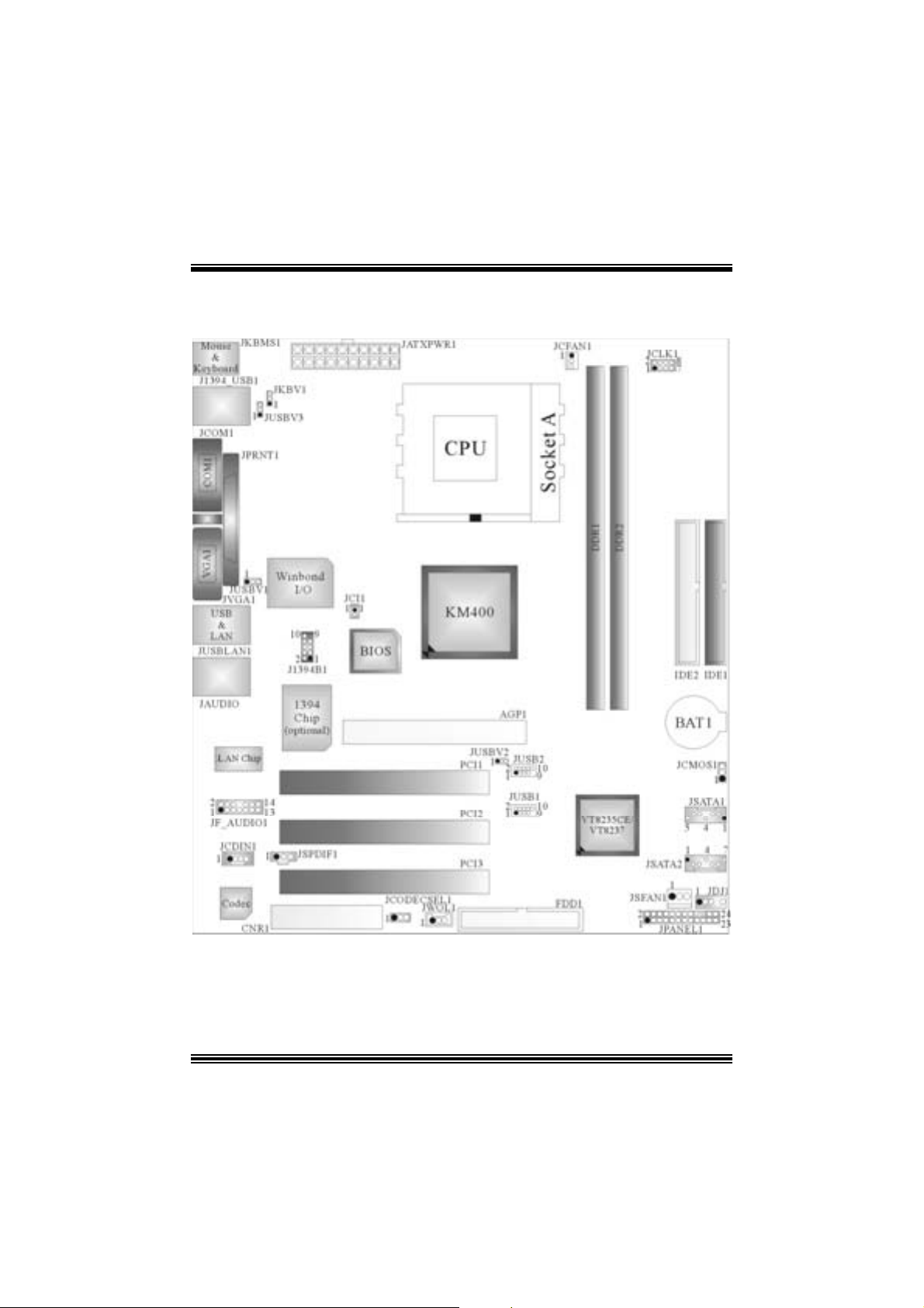
Layout of M7VIZ (V ersion 1.3)
NOTE: ●represents the first pin.
1
M
M
M
Z
I
V
7
Z
I
V
7
Z
I
V
7
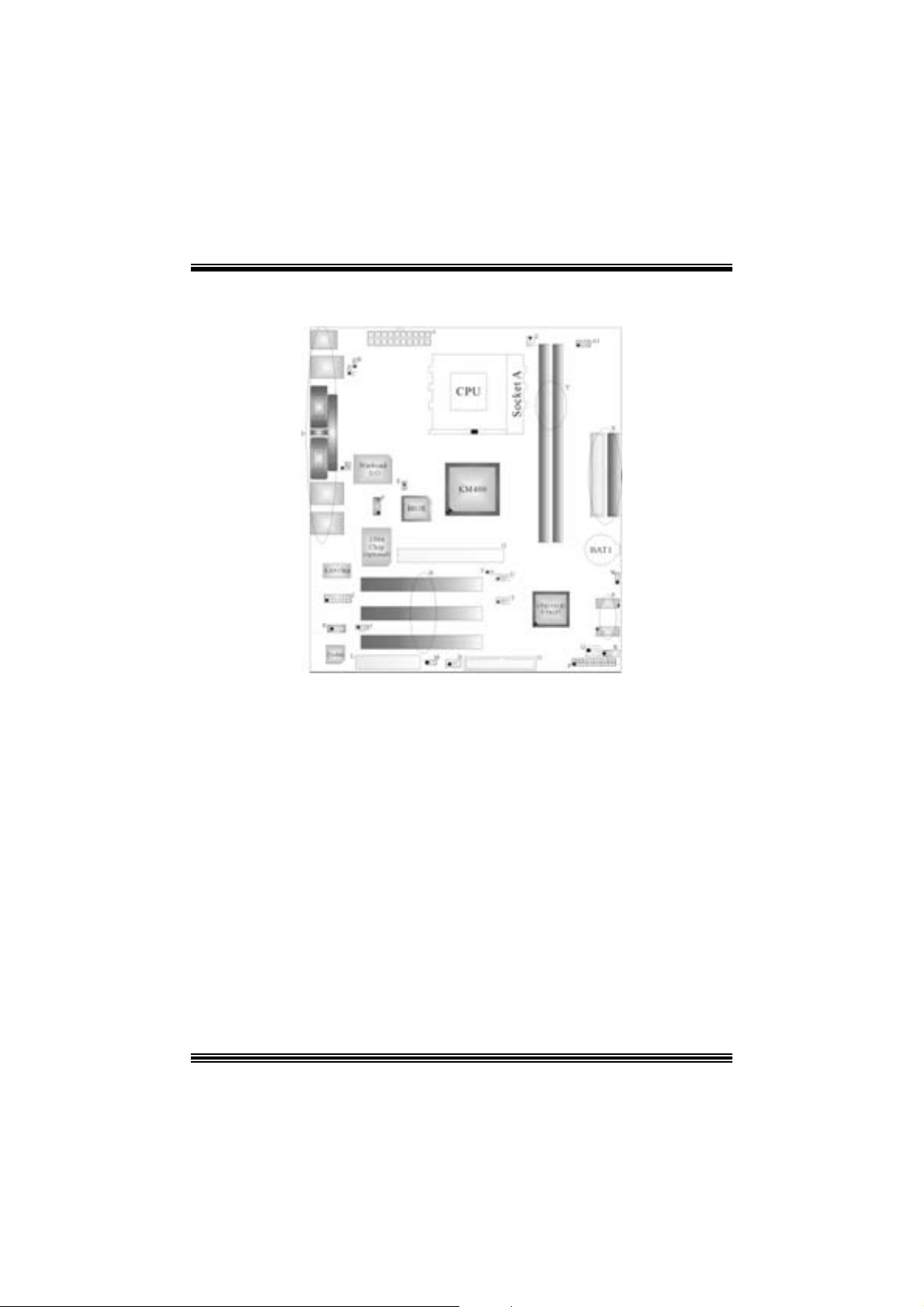
Component Index (Version 1 .3)
A. ATX Power Connector (JATXPWR1) O. Floppy Dis k Connector (FDD1)
B. Power Source Selec tion for Keyboard and
Mouse (JKBV1)
C. Power Source Selection for USB (JUSBV3) Q. Sy stem FAN Header (JSFAN1)
D. B ack Pane l Connec to r R. Au dio DJ (JDJ1)
E. Case Open Conn ector (JCI1) S. Serial ATA C onnector (JSA TA1-2) ◎
F. Front 1394 Header (J1394B1) * T. Front USB Head er (JUSB 1 ) ◎
G. Accelerated Graphics Port Slot (AGP1 U. Front USB Header (JUSB2)
H. PCI BUS Slots (PCI1-3) V. Power Source Selection for USB (JUSBV2)
I. Front Audio Header (JF_AUDIO1) W. Clear CMOS Func tion (JCMOS1)
J. Digital Audio Connector (JSPDIF1) X. IDE Connectors (IDE1-2)
K. CD-ROM Audio-In Hea der (J CDIN1) Y. DDR M odules (DDR1-2)
L. Communic ation Networ k Riser Slot (CNR1) Z. CPU Fan Connector (JCFAN1)
M. CNR Codec/ Onboard Selec tion
(JCODECSEL1)
N. Wake On LAN Header (JWOL1) B1. Power Source Selection for USB (JUSBV1)
* optional
◎ only support with South Bridge VT8237
P. Front Panel Connector (JPANE L1)
A1. Frequency Selection (JCLK1)
2
M
M
M
Z
I
V
7
Z
I
V
7
Z
I
V
7
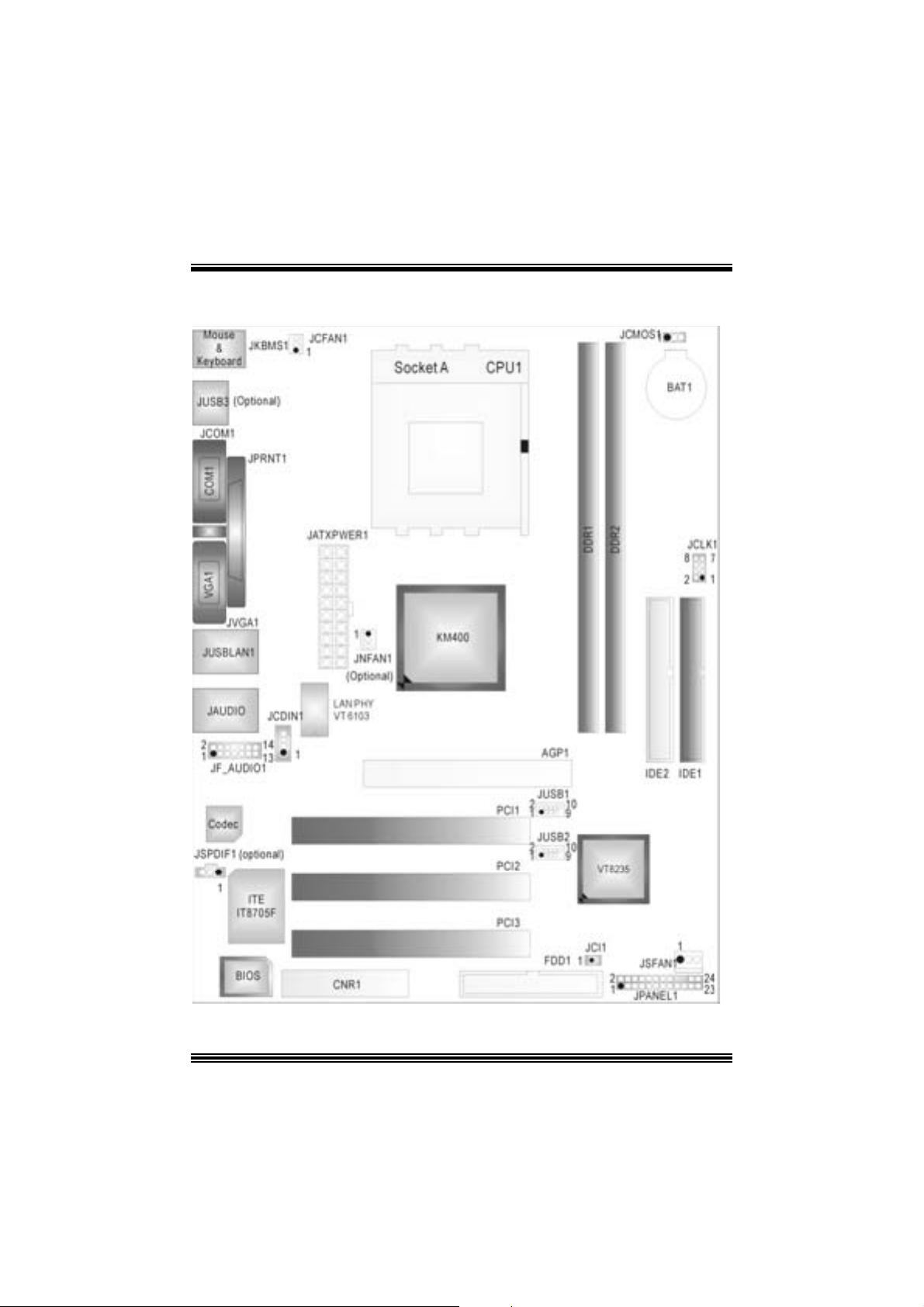
Layout of M7VIZ (V ersion 8.0)
NOTE: ●represents the first pin.
3
M
M
M
Z
I
V
7
Z
I
V
7
Z
I
V
7
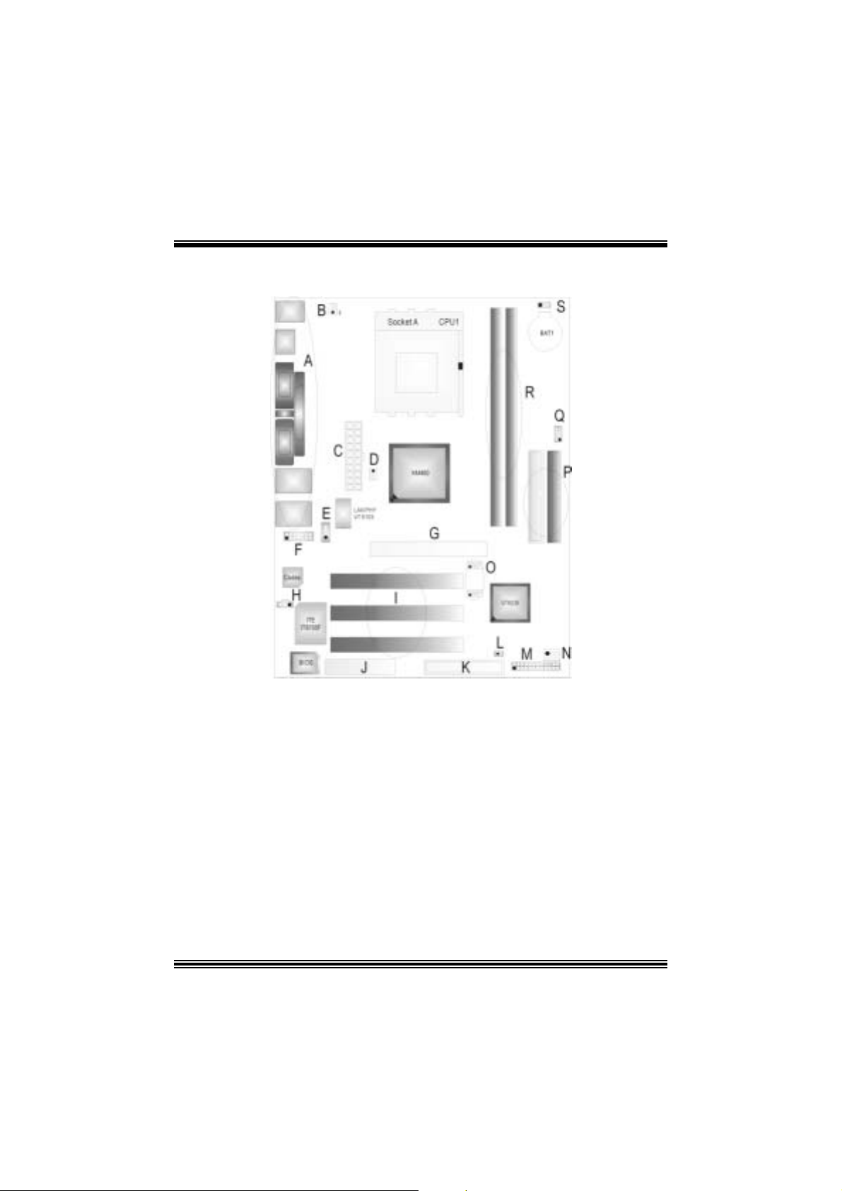
Component Index (Version 8 .0)
A. Back Panel Connectors K. Floppy Dis k Connector (FDD1)
B. CPU Fan Connector (JCFAN1) L. Case Open Connector (JCI1)*
C. ATX Power Connector (JATXPWER1) M. Front Panel Connect or (JPANEL1)
D. North Bridge Fan Con nector (JNFA N1)* N. System FAN Heade r (J SFAN1 )
E. CD-ROM Audio-In Hea der (JCDIN1) O. Front USB He aders (JUSB1 & J USB 2)
F. Front Audio Header (JF_AUDIO 1) P. IDE Connect ors (IDE1-2)
G. Accelerated Graphics Port Slot (AGP1) Q . Freque ncy Selection (JCLK1)
H. Digit al Au dio Conne cto r (JSPDIF1)* R. DDR Modules (DDR1-2)
I. PCI BUS Slots (P CI 1-3) S. Clear CMOS Func tion (JCMOS1)
J. Communication Networ k R iser Slot (CNR1)*
* optional
4

M
M
M
Z
I
V
7
Z
I
V
7
Z
I
V
7
English
M7VI Z Feat u res
A. Har dware
CPU
Prov i d es Soc k et A.
Su pports single AMD® At hlon/ Duron Fam ily proc ess or.
F ront Side Bus at 200/266/333 MHz.
Chipset
N orth Bridge: VIA KM400.
South Bridge: VIA VT8235C E/ VT8237. (optional)
Main Me m o ry
Supports up t o 2 DDR devices.
Supports SPD DDR 200/ 266/333/ 400 MH z (without ECC) DDR devices
Maxi mu m me mo ry s i ze is 2GB.
Super I/O
Chip: Winbond W83 697H F (V ersion 1. 3).
ITE8705F (Version 8.0)
Slots
Three 32-bit PCI bus master s lots.
One CNR slot. (only Ty pe B)
One AGP 8X slot.
On Board IDE
Supports four IDE di s k dri ves.
Supports PIO Mode 4, Master Mode and Ult ra DMA 33/ 66/100/ 133 Bus Mast er
Mode.
LAN PHY
C hip: VIA VT6103.
Supports 10 Mb/s and 100 Mb/ s auto-negot iat ion
Hal f/Full du plex cap ability.
IEEE 1394 Chi p (Option al for Version 1. 3. None for Version 8.0)
C hip: VIA VT6307.
Supports 2 I EEE 1394 port s.
D etects connect ed device ty pes and aut omatically c onfigure data speed to 100,
200 or 400 Mbps.
On Bo ard AC’97 Sound Cod ec
Chip: C MI9761A.
Compliant with AC ’97 s pec ificat ion.
Support s 6 c hannels.
5

M
M
M
On Board Periphera ls
a. R e ar si de
1 s erial port .
1 VGA port.
1 parallel port. (SPP/EPP/ECP m ode)
Audio ports in v ert ical posit ion.
1 R J -45 LAN jack.
PS/2 mouse and PS/2 keyboard.
2 U SB2. 0 ports. (4 U SB2.0 ports only s upport with South Bridge VT8237)
1 1394A Firewire ports. (Optional for Version 1.3, none for Version 8.0)
b. F ront Si d e
1 floppy port supports 2 F DDs with 360K, 720K, 1.2M, 1. 44M and 2.88Mby t es.
4 USB2.0 port s.
1 front audio header.
1 S/PDIF out header.
1 1394A Firewire port s. (Optional for Version 1.3, none for vers ion 8.0)
Dimensions
ATX F orm Factor: 22.1 X 24.5cm (W X L, for v ersion 1.3)
19. 4 X 24.4cm (W X L, f or version 8.0)
Z
I
V
7
Z
I
V
7
Z
I
V
7
B. BIOS & S oftware
BIOS
Award legal BI OS.
Support s APM1.2.
Support s AC PI.
S upports USB Func tion.
Software
Supports Warpspeeder™, 9t h Touch™, FLASHER™
Offers the highest perf orm anc e for Windows 98 SE, W indows 2000, W indows Me,
Windows XP, SC O UNIX etc.
Package contents
HDD Cable X 1
FDD Cable X 1
User’s Manual X 1
Fully Setup Driver CD X 1
USB 2.0 Cable X 1 (optional)
S/ PD IF out Cable X 1 (opt ional)
Rear I/ O Panel for Mic ro ATX C as e X 1 (optional)
IEEE 1394 C able X 1 (opt ional, none f or Vers ion 8.0)
6
M
M
M
Z
I
V
7
Z
I
V
7
Z
I
V
7
How to s e t u p Jumper
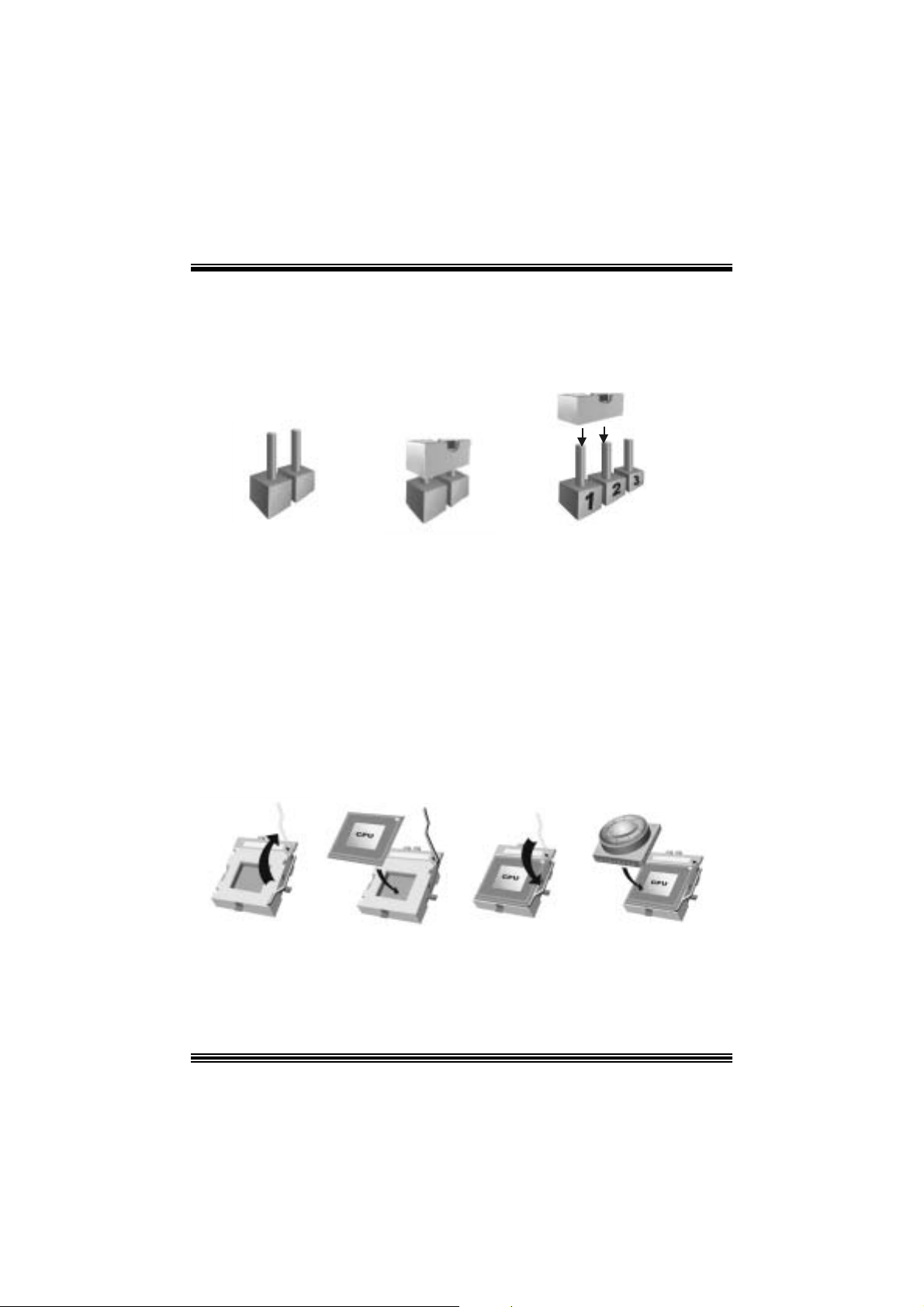
The illustration s hows to how set up jumper. When the J umper c ap is placed on pins, the
jumper is “close”. If no jumper cap is placed on the pins, the jumper is ”open”. The
illust rat ion shows a 3-pin jum per whose pin1and 2 are “clos e” when jumper c ap is plac ed
on thes e 2 pins .
Jumper open Jum per close Pin1-2 close
CPU Installation
Step1: Pull the lever sideway s away from the socket and then raise the lev er up to a
90 -degree angl e.
Step2: Look for the whit e dot /cut edge. The whit e dot/ cut edge should point wards the lever
piv ot. The C P U will f it only in the correct orient at ion .
Step3: Hold the CPU down fir mly, an d then cl ose the lever to complete the installation.
Step4: Put the CPU Fan on the C PU and buckle it. Connect the C PU fan power cable to
the JCFAN1. This completes the installation.
Ste p 1 Step2 Step3 Step4
7
M
M
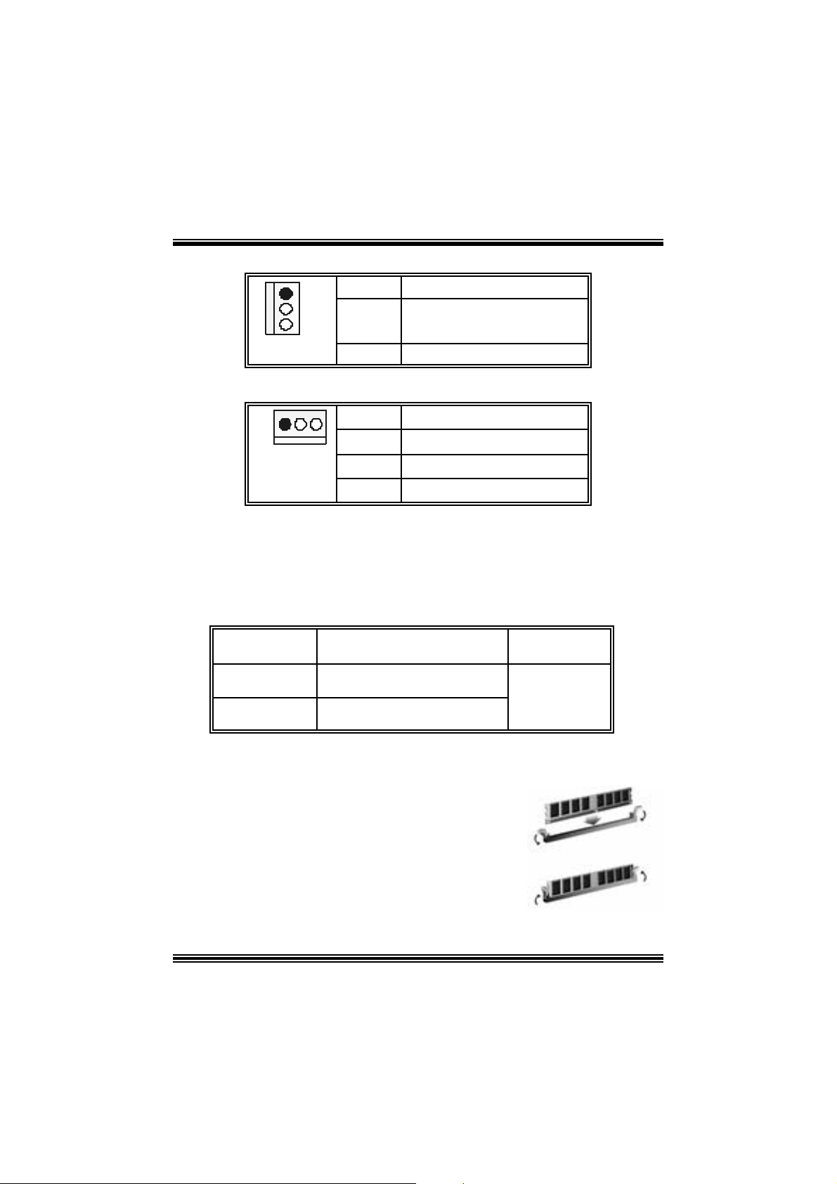
CPU Fan Header: JC FAN1
M
Z
I
V
7
Z
I
V
7
Z
I
V
7
1
JCFAN1
Pin Assignment
1
2
3
Ground
+12V
FAN RPM rate Sense
S ystem Fan Header: JSFAN1
1
JSFAN1
Pin Assignment
1
2
3
FAN RPM rate Sense
Ground
+12V
DDR DI MM Module s: DDR1, DDR2
DRAM Access Time: 2.5V Unbuffered/ R egis t ered DDR 200 MHz (PC 1600)/
DDR 266 MH z (PC 2100)/ DDR 333 MH z (PC 2700) Ty pe required.
DRAM Ty pe: 64MB/ 128MB/ 256MB/ 512MB/ 1GB DI MM Module (184 pin)
DIMM Socket
Location
DDR 1 64MB/128MB/256MB/ 512MB/ 1GB
DDR 2 64MB/128MB/256MB/ 512MB/ 1GB
DDR M odule Total Memory
Size (MB)
*1
*1
***Onl y fo r ref e r e n ce** *
Max is
2GB
Installing DDR Module
1. Unloc k a DIMM slot by pressing the retaining clips
o ut wa rd. Ali gn a D I MM on t h e sl ot s uc h t hat t he
notc h on the DIMM matches the break on the slot.
2. Ins ert the DI MM vertically and f irmly int o the s lot
until the retaining chip snap back in place and the
DIMM i s properly seated.
8

M
M
M
Z
I
V
7
Z
I
V
7
Z
I
V
7
Jumpers, Headers, Connectors & Slots
Floppy Disk Connector: FDD1
The mot herboard provides a standard f loppy disk connector that supports 360K,
720K, 1.2M, 1.44M and 2.88M floppy disk types. This connector supports the
prov ided f loppy drive ribbon cables .
Hard Disk Connectors: IDE1/ IDE2
The motherboard has a 32-bit Enhanced PCI IDE Controller that provides PIO
Mode 0~5, Bus Mast er, and U ltra DMA 33/ 66/ 100/ 133 functionality. It has t wo
HDD connec t ors IDE1 (primary) and IDE2 (secondary).
The ID E c onnectors can c onnect a master and a slav e driv e, so y ou can connect
up t o f our hard dis k driv es . The f irs t hard drive s hould alway s be c onnected to
IDE1.
Peripheral Component Interconnect Slots: PCI 1-3
This m ot herboard is equipped with 3 standard PCI s lots. PCI st ands for Peripheral
Component I nterconnec t, and it is a bus standard for expansion cards. This PCI
slot is des ignated as 32 bits.
Accelerate d Graphics Port Slot: AGP1
Your monitor will attach directly to that video card. This motherboard supports
video cards f or PC I s lots, but it is als o equipped with an Accelerated Graphics Port
(AGP). An AGP card will t ake adv antage of AGP t echnology f or improved v ideo
efficiency and perform ance, es pecially with 3D graphics.
Commun ication Netwo r k R ise r Slot: CNR1
The CNR specification is an open I ndust ry St andard Architecture, and it defines a
ha rdw ar e scalable r iser card interfa ce, which su pports modem only.
Serial ATA Co nnector: JSATA1/ JSATA2 (only support wit h
South Bridge VT8237)
The mot herboard has a PCI to SATA C ontroller with 2 channels SATA interf ace, it
satisfies the SATA 1.0 spec and can transf er data wit h 1. 5 Gb/s speed.
Note:
1. When plugging SATA HDD on JSATA1 connector, SATA BIOS will
auto ma tically detect as channel 1.
2. When plugging SATA HDD on JSATA2 connector, SATA BIOS will
auto ma tically detect as channel 0.
9

M
M
M
Z
I
V
7
Z
I
V
7
Z
I
V
7
Front Pane l Conne ctor: JPANEL1
SLP
JPANEL1
Pin Assignment Function Pin Assignment Function
1 +5V 2 Sleep Control
3 NA 4 Ground
5 NA 6 NA NA
7 Speaker
9 HD D LED (+ ) 10 Power LED (+)
11 HDD LED (-)
13 Ground 14 Power Butt on
15 Reset Control
17 NA 18 KEY
19 NA 20 KEY
21 +5V 22 Ground
23 IRTX
2
1
PWR_LED
SPK
HLED
RST
Speaker
Connector
8 Power LED (+)
Hard Drive
LED 12 Power LED (-)
Reset
Button 16 Ground
IrDA
Connector
24 IRRX
IRON/OFF
IR
24
23
Sleep
Button
POWER
LED
Power-on
Button
IrDA
Connector
Power Conn ectors: JATXPWR1
20 11
10
JATXPWR1
1
PIN Assignment PIN Assignment
1
2
3
4
5
6
7 Ground 17 Ground
8
9
10
+3.3V
+3.3V
Ground
+5V
Ground
+5V
PW_OK
St andby Volt age
+5V
+12V
10
11
12
13
14
15
16
18
19
20
+3. 3V
-12V
Ground
PS_ON
Ground
Ground
-5V
+5V
+5V
M
e
1
M
M
Z
I
V
7
Z
I
V
7
Z
I
V
7
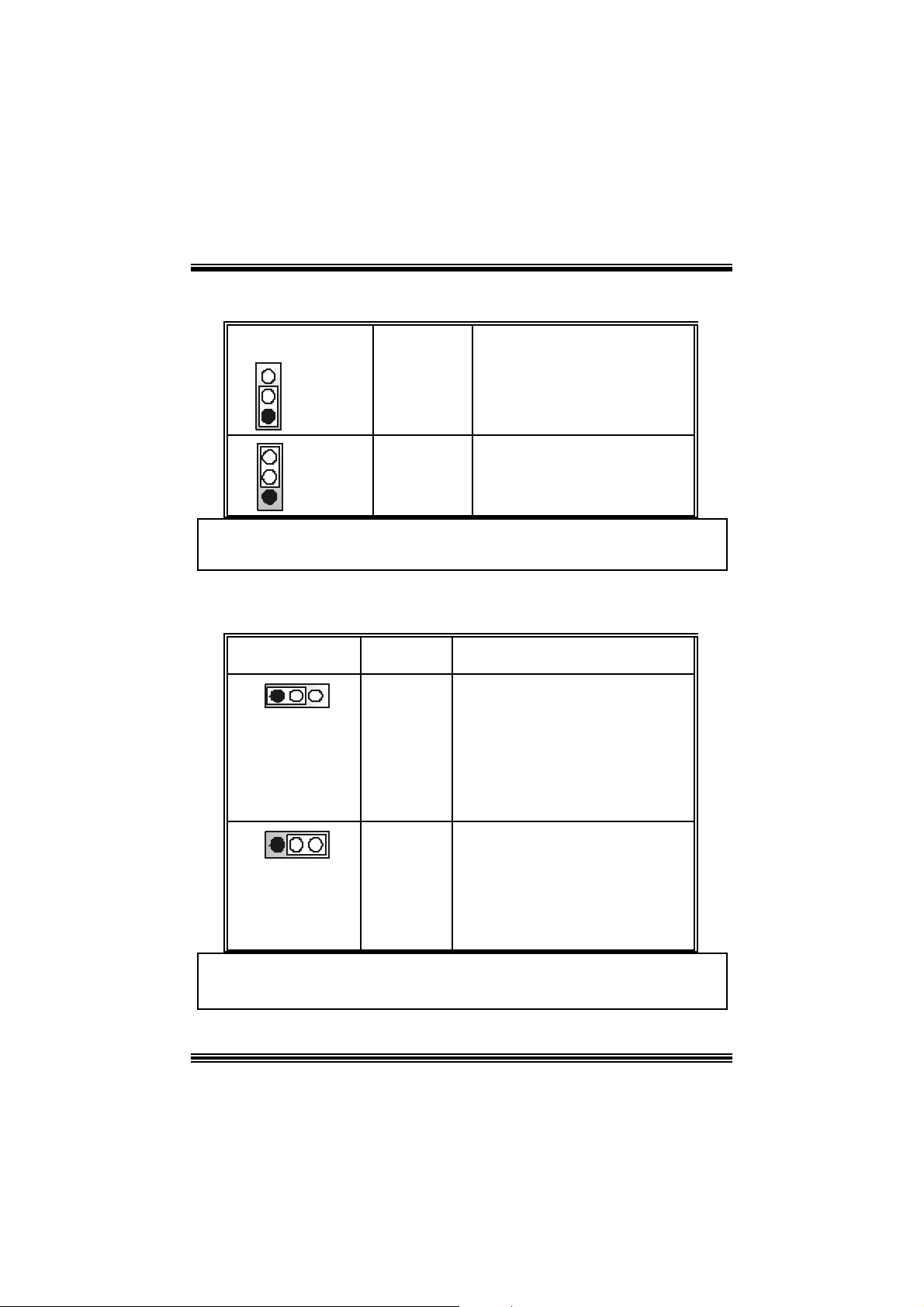
Power Source Selection for Keyboard/ Mo use: JKBV1 (N o support
for version 8.0)
JKBV1 Assignment Description
3
+5V
1
Pin 1-2 close
3
+5V Standb y
1
Pin 2-3 close
Note: In order to support the function “power-on the system via keyboard and
mouse function, “JKBV1” jumper cap should be placed on pin 2-3.
Voltage
+5V for keyb oard and mouse
PS/2 Mous e and PS/2 Key board ar
powered with +5V standby v oltage
Power Source Selection for US B: JUSBV1/ JUSBV2 / JUSBV3 (No
su pport for version 8.0)
JUSBV1/JUSBV2/
JUSBV3
1 3
Pin 1-2 c los e
Assignment Description
+5V JUSBV3: 5V f or USB at the 1394_USB
port c onnec t or
JUSBV2: 5V for US B a t the JUSB2 port
connector
JUSBV1: 5V for US B a t the JUSBLA N 1
port c onnec t or
1 3
Pin 2-3 c los e
Note: In order to support the function “power-on the system via USB devi ces
function, “JUSBV1/JUSBV2/ JUSBV3” jumper cap should be placed on pin
2-3 respectively.
+5V Standby
Voltage
JUSBV3: J1394_ USB1 port is powered
with s t andby v olt age of 5V
JUSBV2: JUSB2 port is powered with
standby v olt age of 5V
JUSBV1: JUSBLAN 1 port is powered
with s t andby volt age of 5V
11
M
M
M
Z
I
V
7
Z
I
V
7
Z
I
V
7
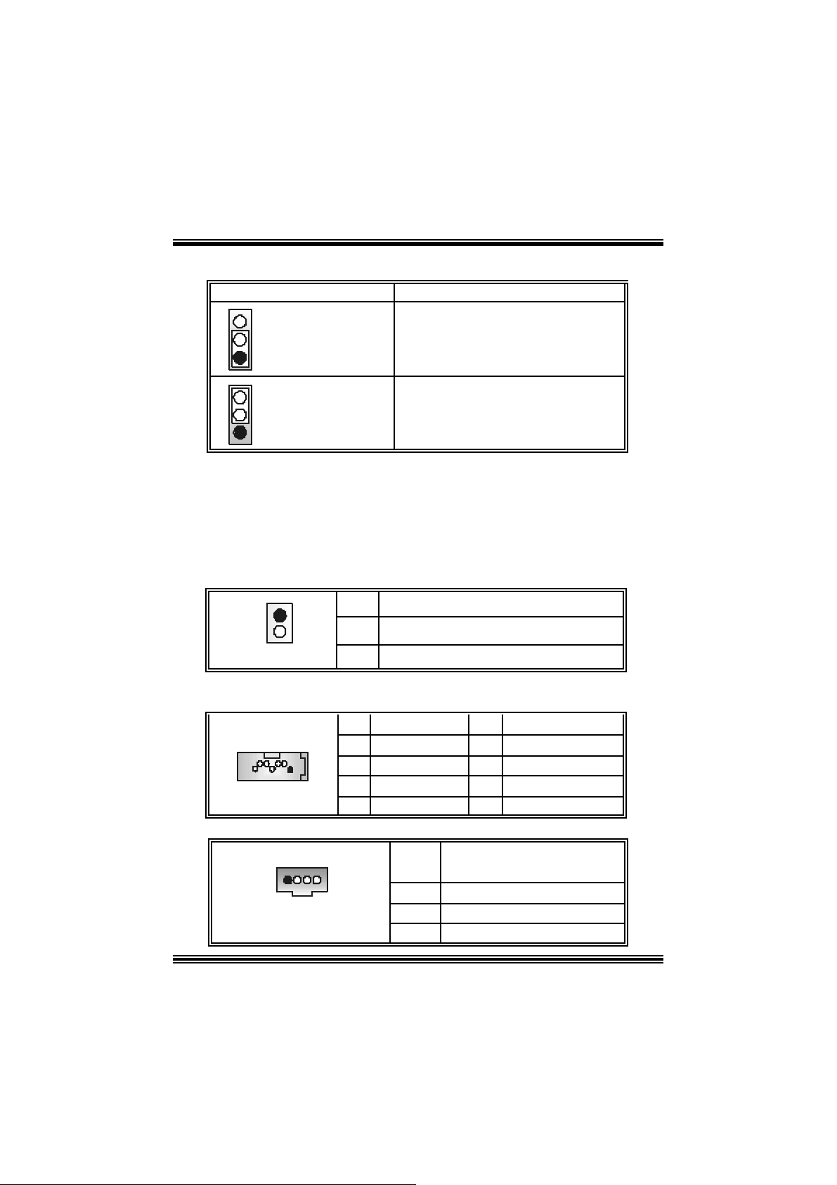
Clear CMOS Jumper: JCMOS1
3
1
3
1
JCMOS1 Assignment
Norm al Operation (def ault)
Pi n 1-2 C lose
Clear CMOS Data
Pi n 2-3 C lose
※ Clear CMOS Procedures:
1. R emov e AC power line.
2. Set the jumper to “Pin 2-3 C lose”.
3. Wa it for fi ve seconds.
4. Set the jumper to “Pin 1-2 C lose”.
5. Power on t he AC .
6. R eset your des ired password or clear t he C MOS dat a.
Ca se Op e n Connec to r: JCI1
1
JCI1
Pin
1
2
Assign ment
Case Open Signal
Ground
Serial ATA Co nnector: JSATA1/ JSATA2 (O nly support with
South Bri dge VT8237)
1234567
JSA TA1/ JSATA2
Pin Assignment Pin Assignment
1
3
5
7
Ground
TXRX-
Ground
2
4
6
TX+
Ground
RX+
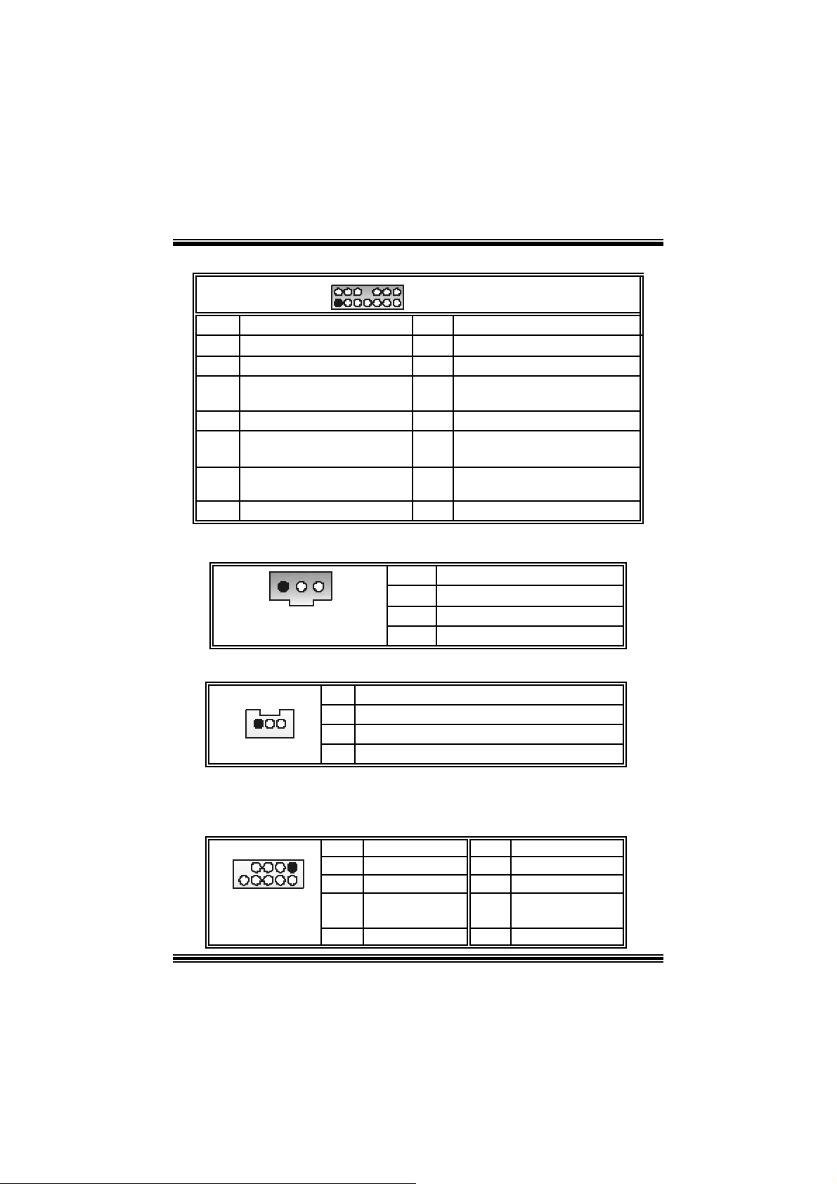
CD-ROM Audio-In Heade r: JCDIN1
1 4
JCDIN1
Pin Assignment
1
2
3
4
12
Left Channel In put
Ground
Ground
Right Channel In put
M
t
M
M
Z
I
V
7
Z
I
V
7
Z
I
V
7
Front Panel Audio Header: JF_AUDIO1
2
1
Pin Assignment Pin Assign m ent
1
3 Mic Power/ Bass 4 Audio Power
5
7
9
11
Left Line I n/ R ear Speak er Left
13
Mic In/ C ent e r
Right Line Out/ Speaker Out
Right
Reserv ed
Left Line Out/ Speak er Out
Left
Right Line I n/ R ear Speaker
Right
14
13
JF_AUDIO1
2
Right Line Out/ Speaker Out Righ
6
8
Left Line Out/ Speaker Out Left
10
Right Line In/ R ear Speaker Right
12
Lef t Line I n/ Rear Speaker Left
14
Ground
Key
Digital Audio Connector: JSPDIF1 (Optional for version 8.0)
13
JSPDIF1 3
Pin Assignment
1
2
+5V
SPDIF_OUT
Ground
Wake On LAN Header: JWOL1 (No support for version 8.0)
1
JWO L1
Pin Assignment
1 +5V_SB
2
3 Wake up
Ground
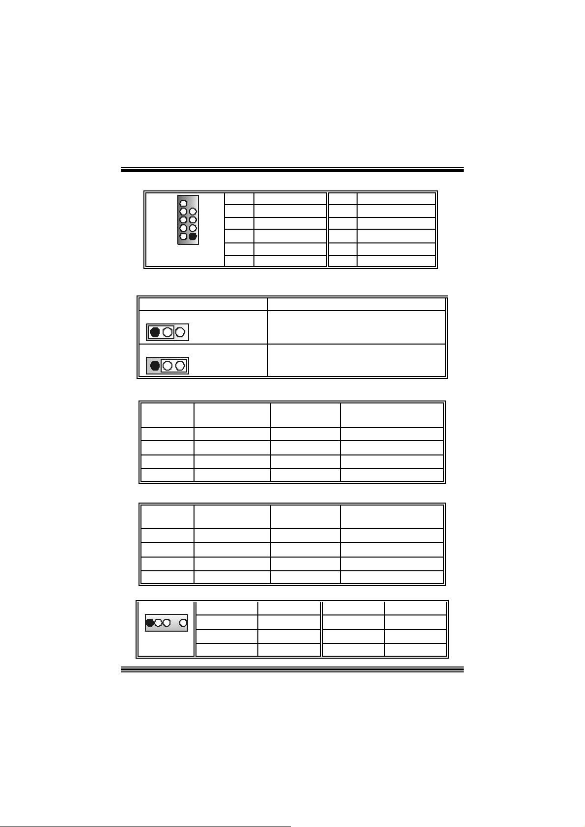
Front USB Header: JUSB2, (JUSB1=>only support with South
Bri dge VT8237)
Note: Version 8.0 supports both JUSB 1 & JUSB2.
9
10
JUSB1/2
Pin Assignment Pin Assignment
1
1
3
2
5
7
9
+5V(fused)
USB-
USB+
Ground
KEY
2
4
6
8
10
+5V(fused)
USB-
USB+
Ground
NC
13
M
M
M
Z
I
V
7
Z
I
V
7
Z
I
V
7
Front 1394 Header: J1394B1
10 9
21
J1394B1
CNR Codec/ Onboard Sel ection: JCOD ECSEL1
JCODECSEL1 Assignment
31
Pin 1-2 C lose
31
Pin 2-3 C lose
Pin Assignment Pin Assignment
1
3 Ground 4 Ground
5
7
9
A+
B+
+12V
KEY
Onboard C odec is used (def ault)
2
6
8
10
CNR Codec is used
Frequency Selection: JCLK1 (Version 1.3)
A-
B-
+12V
Ground
Pin 100 MHz 133 MHz
(Default)
1-2
3-4
5-6 Open Open Close
7-8
Open Open Open
Close Open Open
Open Open Open
166 MHz
Frequency Selection: JCLK1 (Version 8.0)
Pin 100 MHz 133 MH z
(Default)
1-2
3-4
5-6
7-8
Close Open Open
Close Close Open
Open Open Open
Open Open Open
166 MHz
Audio DJ: JDJ1
15
JDJ1
Pin Assignment Pin Assignment
1
3
5
SMBDT
-INTR_B
PWRGD
14
2
4
SMBCK
NA
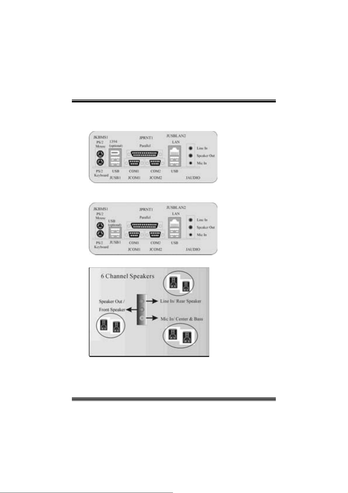
B ack Panel Connectors
For vers ion 1.3
For vers ion 8.0
M
M
M
Z
I
V
7
Z
I
V
7
Z
I
V
7
15

Trouble Shoo ting
e
e
r
y
plugg
e
g up
y
pp
a
prog
e
r
PROBABLE SOLUTION
No power to the system at all Power light don’t
illuminate, fan inside power supply does not turn
on. Indicator light on keyboard does not turn on
PROBABLE SOLUTION
System inoperative. Keyboard lights are on,
power indicator lights are lit, hard drive is
sp in ning.
PROBABLE SOLUTION
System does not boot from hard disk dri ve, can
be booted from CD-ROM drive.
PROBABLE SOLUTION
System only boots from CD-ROM. Hard disk can
be read and applications can be used but
booting from hard disk is i mpossible.
M
M
M
Z
I
V
7
Z
I
V
7
* Make sure power cable is securely plugged i n
* Repl ac e c abl e
* Contac t techni cal s uppo rt
* Using even pressure on both ends of th
DIM M, press down firmly until the modul
snaps into p la ce.
* Check cable running from disk to dis k controlle
board. Make sure both ends are securel
ed in; check the drive type in th
standard CMOS setup.
* Backin
important. All hard disks are capable o
breaking down at any time.
* Bac k up data and applications files. Reforma
the hard drive. Re-install a
using backup dis ks.
the hard drive is extremel
l icat ions and dat
Z
I
V
7
PROBABLE SOLUTION
Screen m essage says “Invalid Configuration” or
“CMOS Failure.”
PROBABLE SOLUTION
Cannot boot s ystem after ins talling second hard
drive.
* Review system’s equipment . Make sure
c or r ect infor m a t io n is in s et u p.
* Set master/slave jum p e rs c o rrectly.
* Run SETUP
types. Call drive manufacturers fo
compatibility wi th other drives.
16
ram and select correct driv

M
M
M
Z
I
V
7
Z
I
V
7
Z
I
V
7
Français
Caractérist iques de l a M7 VIZ
A. Maté ri e l
Processeur
F ournit un support Socket A.
Prend en charge un unique processeur AMD® de la famille At hlon/ D uron.
Bus face avant à 200/266/333 MHz.
Chipset
Pont nord : VIA KM400.
Pont sud : VIA VT8235CE/ VT8237.(opt ion)
M é moire prin cipa le
Prend en charge 2 barrettes DDR .
Prise en charge des périphériques SPD DDR 200/266/333/400 MH z (s ans ECC).
Taille max imale de mémoire : 2 Go.
Super E/S
Puc e : Winbond W83697HF. (Version 1. 3)
ITE8705F . (Vers ion 8.0)
Expansion
Trois em plac ements PCI 32 bit s bus maît re.
U n emplacement C NR . (Ty pe B uniquem ent)
Un em placem ent AGP 8X.
IDE in tégré
Prend en charge quat re lecteurs de disques IDE.
Prend en charge les modes PI O 4, Maître et bus maître Ult ra D MA 33/66/100/133.
Réseau
Puce : VIA VT6103.
Prend en charge la négociation aut omat ique 10 Mb/s et 100 Mb/s
C apacité semi duplex/ duplex com plet.
Puce IEEE 1394 (Optio n, Versio n 8 . 0 non p rise en charge)
Puce : VIA VT6307.
Prend en charge 2 ports IEEE 1394.
D étecte les périphériques connectés et configure automat ique la vit esse de
transfert des données à 100, 200 ou 400 Mb/s.
Codec son AC’97 int égré
Puc e : CMI 9761A.
Conf o r m e à la spécif ica t ion AC’ 97.
Prend en charge 6 canaux.
17
 Loading...