

Biostar M7VIT Owner's Manual

M
7
V
I
T
V
V
I
T
I
T
M
M
7
7
FCC Statement and Copyright
This equipment has been tested and found to comply with the limits of a
Class B digital device, pursuant to Part 15 of the FCC Rules. These limits
are designed to provide reasonable protection against harmful interference
in a residential installation. This equipment generates, uses and can
radiate radio frequency energy and, if not installed and used in
accordance with the instructions, may cause harmful interference to radio
communications. There is no guarantee that interference will not occur in a
particular installation.
The vendor makes no representations or warranties with respect to the
contents here of and specially disclaims any implied warranties of
merchantability or fitness for any purpose. Further the vendor reserves the
right to revise this publication and to make changes to the contents here of
without obligation to notify any party beforehand.
Duplication of this publication, in part or in whole is not allowed without
first obtaining the vendor’s approval in writing.
The content of this user’s is subject to be changed without notice and we
will not be responsible for any mistakes found in this user’s manual. All the
brand and product names are trademarks of their respective companies.
i

C
o
n
t
e
n
t
s
C
o
n
C
o
n
ENGLISH..................................................................................................... 1
M7VIT Features ..................................................................................................................1
Package contents .............................................................................................................. 2
Layout of M7VIT.................................................................................................................3
CPU Installation ................................................................................................................. 4
DDR DIMM Modules: DIMM1-2-3 ...................................................................................... 5
Jumpers, Headers, Connectors & Slots .......................................................................... 7
t
e
n
t
s
t
e
n
t
s
ESPAÑOL ................................................................................................. 12
Características del M7VIT ............................................................................................... 12
Contenido del Paquete.................................................................................................... 13
Disposición del M7VIT .................................................................................................... 14
Instalación de la CPU ...................................................................................................... 15
Módulos DDR DIMM: DIMM1-2-3 .................................................................................... 16
Puentes, Cabezales, Conectores y Ranuras................................................................. 18
WARPSPEEDER ...................................................................................... 23
Introduction...................................................................................................................... 23
System Requirement....................................................................................................... 24
Installation........................................................................................................................ 24
Usage................................................................................................................................ 26
TROUBLE SHOOTING............................................................................. 34
SOLUCIÓN DE PROBLEMAS ................................................................. 35
ii

M
o
t
h
e
r
b
o
a
r
d
D
e
s
c
r
i
p
t
i
o
n
M
M
o
t
h
e
r
b
o
a
r
d
D
e
s
c
r
o
t
h
e
r
b
o
a
r
d
D
i
e
s
c
r
p
t
i
o
n
i
p
t
i
o
n
English
M7VIT Features
Use VIA VT8377 (KT400)/ VT8235 Chipset, Winbond W83697HF.
Contains on board I/O facilities, which include two serial ports, a parallel
port, a PS/2 mouse port, a PS/2 keyboard port, audio ports, USB ports, a
game port.
Supports Single Socket-A for an AMD Athlon/ Duron Family processor,
running at 200/266/333 MHz Front Side Bus frequency.
The AMD Athlon/ Duron system bus supports the 200/266/333 MHz
high-speed, split-transaction AMD Athlon/ Duron system bus interface.
Supports Ultra DMA 33/66/100/133 Bus Master Modes, PIO Mode 4,
Master Mode, and high performance hard disk drives.
Supports USB2.0 6 ports High Speed Device, 2 ports in Rear Panel and 4
ports in Front Panel.
The VT8377 (KT400) system controller is designed to support
200/266/333/400 MHz DDR SDRAM DIMMs.
Support a maximun memory size up to 3GB.
Supports one CNR Slot (Type B only), one AGP 4X/ 8X Slot, and five 32-bit
PCI Bus slots.
Complies with PC ATX form factor specifications.
Supports popular operating systems such as Windows NT, Windows 98SE,
Windows 2000, Windows ME, Windows XP and LINUX.
CPU over temperature protection.
Intel® AC’97 2.2 compatible. High S/N ratio meets PC 99 requirements.
Line-in phonejack and Mic-in jack share with rear Audio out for 6 channels
Audio.
6-Channel Hardware Audio or Codec. (Change Line-In to Back-Audio Out
and Mic-In to Bass/ Center Out by Audio Utility.) (Optional)
1

M
o
t
h
e
r
b
o
a
r
d
D
e
s
c
r
i
p
t
i
o
n
M
o
t
h
e
r
b
o
a
r
d
M
o
t
h
e
r
b
Support Front Audio pin head functions.
D
o
a
r
d
D
e
s
c
r
i
e
s
c
r
p
t
i
o
n
i
p
t
i
o
n
CMI 8738 Hardware Audio Features (Optional):
* 6CH DAC for AC3® 5.1CH purpose.
* HRTF-based 3D positional audio, supporting DirectSound™ 3D and
A3D™ interface.
* Supports 4.1/5.1 speakers, C3DX positional audio in 4/ 6 CH speaker
mode.
* MPU-401 port.
* Built-in ZV port.
Package contents
HDD Cable X 1, FDD Cable X 1, Fully Setup Driver CD X 1
Flash Memory Writer for BIOS update X 1
USB Cable X 2 (Optional)
Rear I/O Panel for ATX Case X 1 (Optional)
2
M
o
t
h
e
r
M
M
b
o
t
h
e
r
b
o
t
h
e
r
b
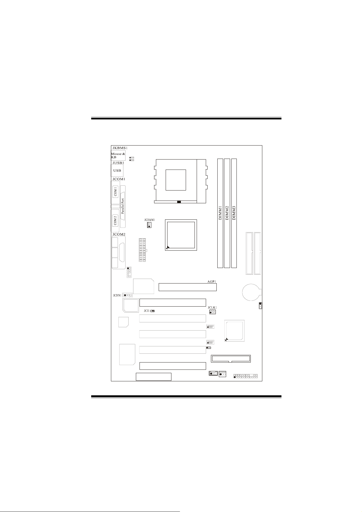
Layout of M7VIT
SP-OUTMIC-IN LINE-IN
JGAME1
Codec
Hardware
Audi o
GAME Port
1
1
1
1
BIOS
JKBV1
JUSBV1
JATXPWR1
JAUDIO1
Winbond
I/O
CPU
1
VT8377
(KT400)
PCI SLOT
1
PCI SLOT
PCI SLOT
PCI SLOT
PCI SLOT
CNR SLOT
o
a
r
d
o
a
r
d
o
a
r
AGP SLOT
CNR1
D
e
s
c
r
i
p
t
i
o
n
D
e
s
c
r
d
D
i
e
s
c
r
p
t
i
o
n
i
p
t
i
o
n
Socket A
IDE1IDE2
2
1
BAT1
JPANEL1
JCMOS1
FDD1
1
24
23
PCI1
PCI2
PCI3
PCI4
PCI5
1
JUSB2
129
JUSB3
129
JUSBV2
1
JWOL1
1
664
3
10
10
VT8235
1
JSFAN1
3
M
o
t
h
e
r
b
o
a
r
d
D
e
s
c
r
i
p
t
i
o
n
M
M
o
t
h
e
r
b
o
a
r
d
D
e
s
c
r
o
t
h
e
r
b
o
a
r
d
D
i
e
s
c
r
p
t
i
o
n
i
p
t
i
o
n
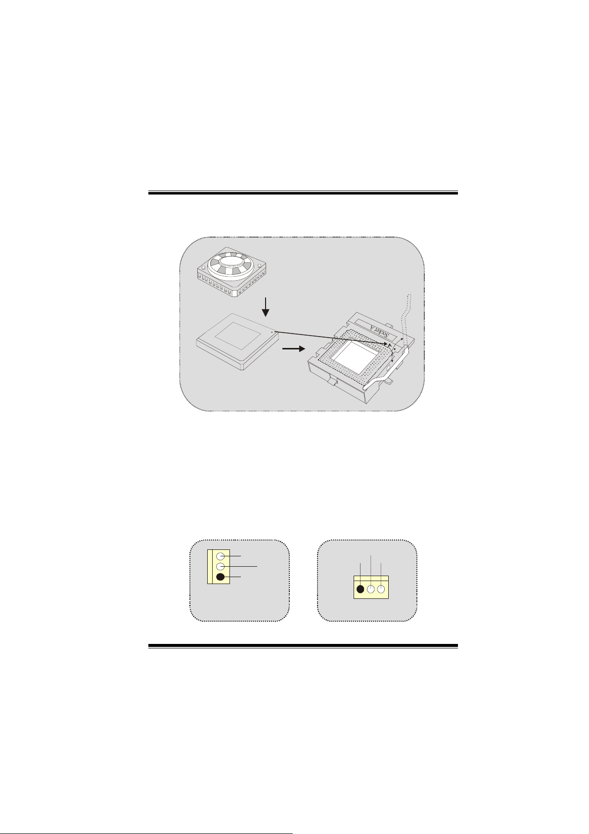
CPU Installation
C
P
U
1. Pull the lever sideways away from the socket then raise the lever up
to 90-degree angle.
2. Locate Pin A in the socket and lock for the white dot or cut edge in
the CPU. Match Pin A with the white dot/cut edge then insert the
CPU.
3. Press the lever down. Then Put the fan on the CPU and buckle it
and put the fan’s power port into the JCFAN1, then to complete the
installation.
CPU/ System Fan Headers: JCFAN1/ JSFAN1
1
JCFAN1
Sense
12V
Ground
Ground
12V
Sense
1
JSFAN1
4
M
o
t
h
e
r
b
o
a
r
d
D
e
s
c
r
i
p
t
i
o
n
M
M
o
t
h
e
r
b
o
a
r
d
D
e
s
c
r
o
t
h
e
r
b
o
a
r
d
D
i
e
s
c
r
p
t
i
o
n
i
p
t
i
o
n
DDR DIMM Modules: DIMM1-2-3
DRAM Access Time: 2.5V Unbuffered/ Registered DDR 1600/ 2100/
2700/ 3200 Type required.
DRAM Type: 64MB/ 128MB/ 256MB/ 512MB/ 1GB DIMM Module (184
pin)
Only support 4 bank for DDR PC3200 (2pcs Double-Side or 3
pcs Single-Side).
DIMM Socket
Location
DIMM 1 64MB/128MB/256MB/512MB/1GB
DIMM 2 64MB/128MB/256MB/512MB/1GB
DIMM3 64MB/128MB/256MB/512MB/1GB
* The list shown above for DRAM configuration is only for reference.
z If use FSB333MHz CPU, the Memory support only
DDR333 (PC2700).
List of the status of DDR 400 already passed
Clock Vender Serial No. (Chip) Module
1 DDR400 KINGMAX KDL684T4AA-50 256M Pass
2 DDR400 SAMSUNG K4H560838D-TCC4 256M Pass
3 DDR400 TwinMOS TMD7608F8E50B 256M Pass
4 DDR400 Winbond W942508BH-5 256M Pass
5 DDR400 Winbond W942508BH-5 512M Pass
DDR Module Total Memory
Size (MB)
*1
Max is
*1
*1
Size
3GB
MEMTEST
5
M
o
t
h
e
r
b
o
a
r
d
D
M
M
o
t
h
e
r
b
o
o
t
h
e
r
b
o
e
a
r
d
D
e
a
r
d
D
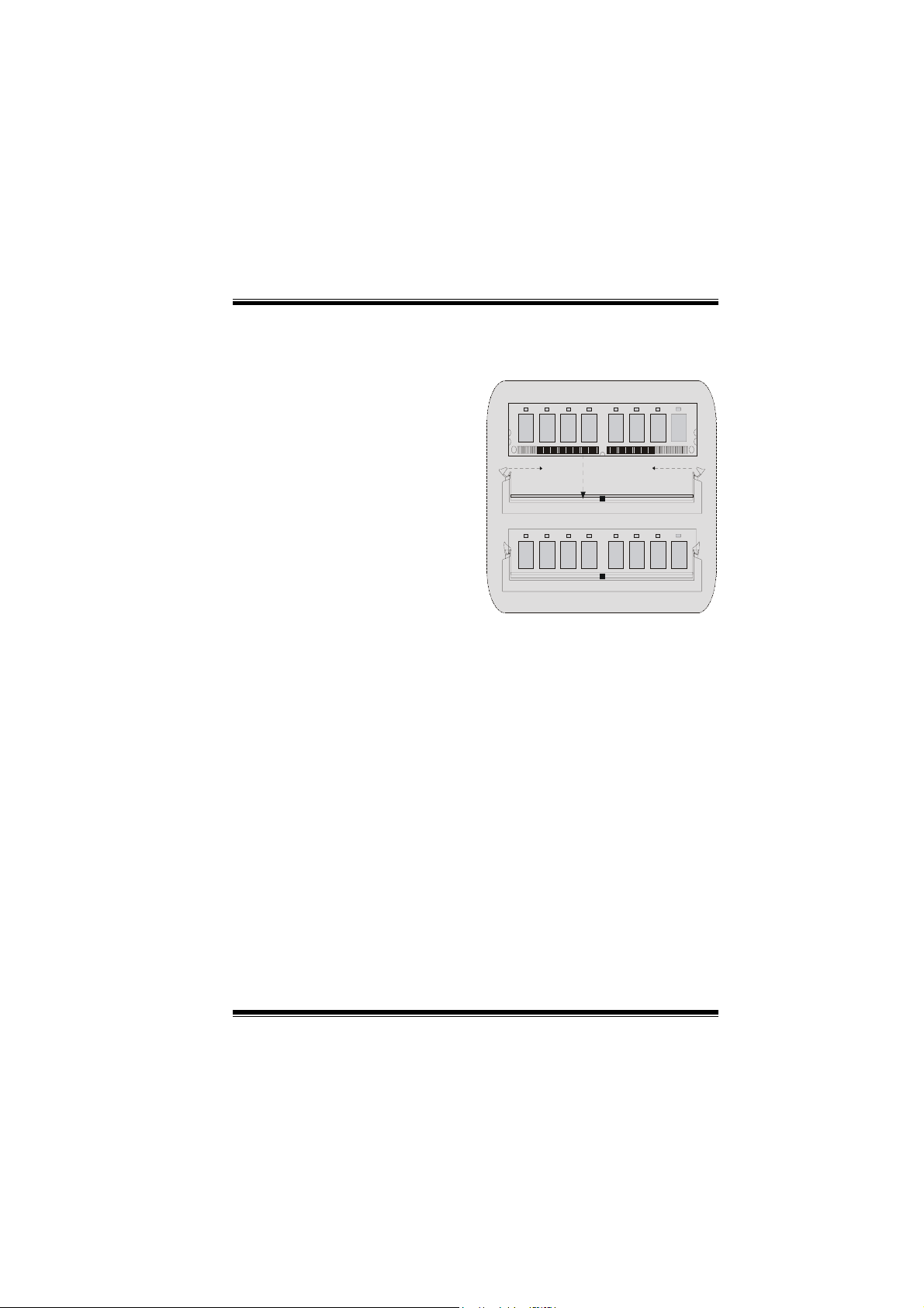
How to install a DIMM Module
1. The DIMM socket has a
“ Plastic Safety Tab”, and the
DIMM memory module has an
“Asymmetrical notch”, so the
DIMM memory module can only
fit into the slot in one direction.
2. Push the tabs out. Insert the
DIMM memory modules into the
socket at a 90-degree angle, then
push down vertically so that it will
fit into the place.
3. The Mounting Holes and plastic
tabs should fit over the edge and
hold the DIMM memory modules
in place.
s
c
r
i
p
t
i
o
n
s
c
r
i
e
s
c
r
p
t
i
o
n
i
p
t
i
o
n
6

M
o
t
h
e
r
b
o
a
r
d
D
e
s
c
r
i
p
t
i
o
n
M
M
o
t
h
e
r
b
o
a
r
d
D
e
s
c
r
o
t
h
e
r
b
o
a
r
d
D
i
e
s
c
r
p
t
i
o
n
i
p
t
i
o
n
Jumpers, Headers, Connectors & Slots
Hard Disk Connectors: IDE1/ IDE2
The motherboard has a 32-bit Enhanced PCI IDE Controller that
provides PIO Mode 0~4, Bus Master, and Ultra DMA 33/ 66/ 100/ 133
functionality. It has two HDD connectors IDE1 (primary), IDE2
(secondary) and IDE3.
The IDE connectors can connect a master and a slave drive, so you can
connect up to four hard disk drives. The first hard drive should always be
connected to IDE1.
Floppy Disk Connector: FDD1
The motherboard provides a standard floppy disk connector that
supports 360K, 720K, 1.2M, 1.44M and 2.88M floppy disk types. This
connector supports the provided floppy drive ribbon cables.
Accelerated Graphics Port Slot: AGP1 (only support AGP
Your monitor will attach directly to that video card. This motherboard
supports video cards for PCI slots, but it is also equipped with an
Accelerated Graphics Port (AGP). An AGP card will take advantage of
AGP technology for improved video efficiency and performance,
especially with 3D graphics.
Communication Network Riser Slot: CNR1
The CNR specification is an open Industry Standard Architecture, and it
defines a hardware scalable riser card interface, which supports audio,
network and modem only.
Peripheral Component Interconnect Slots: PCI1-5
This motherboard is equipped with 5 standard PCI slots. PCI stands for
Peripheral Component Interconnect, and it is a bus standard for
expansion cards, which has, supplanted the older ISA bus standard in
most ports. This PCI slot is designated as 32 bits.
power 1.5V)
7
M
o
t
h
e
r
b
o
a
r
d
D
e
s
c
r
i
p
t
i
o
n
M
M
o
t
h
e
r
b
o
a
r
d
D
e
s
c
r
o
t
h
e
r
b
o
a
r
d
D
i
e
s
c
r
p
t
i
o
n
i
p
t
i
o
n
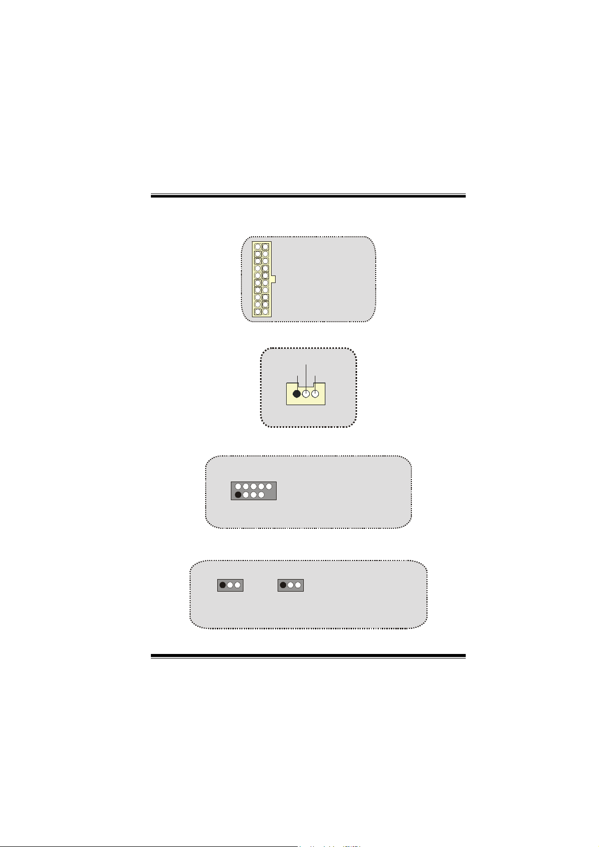
Power Connectors: JATXPWR1
JATXPWR1
(ATX Main Power Conn.)
JATXPWR1
(ATX Power Conn.)
Wake On LAN Header: JWOL1
Ground
5V_SB Wake up
1
JWOL1
Front USB Header: JUSB2/3
2
1
JUSB2/3
Pin1,2 ==> +5V
Pin3,4 ==> Data(-)
Pin5,6 ==> Data(+)
Pin7,8 ==> Ground
Pin9 ==> KEY
Pin10 ==> NA
5V/ 5VSB Selection for USB/KB: JUSBV1/2/ JKBV1
JUSBV1/2
1
1
JKBV1
Pin 1-2 on ==> 5V
Pin 2-3 on ==> 5V_SB
8
M
o
t
h
e
r
b
o
a
r
d
D
e
s
c
r
M
M
o
t
h
e
r
b
o
a
r
d
o
t
h
e
r
b
D
o
a
r
d
D
i
e
s
c
r
i
e
s
c
r
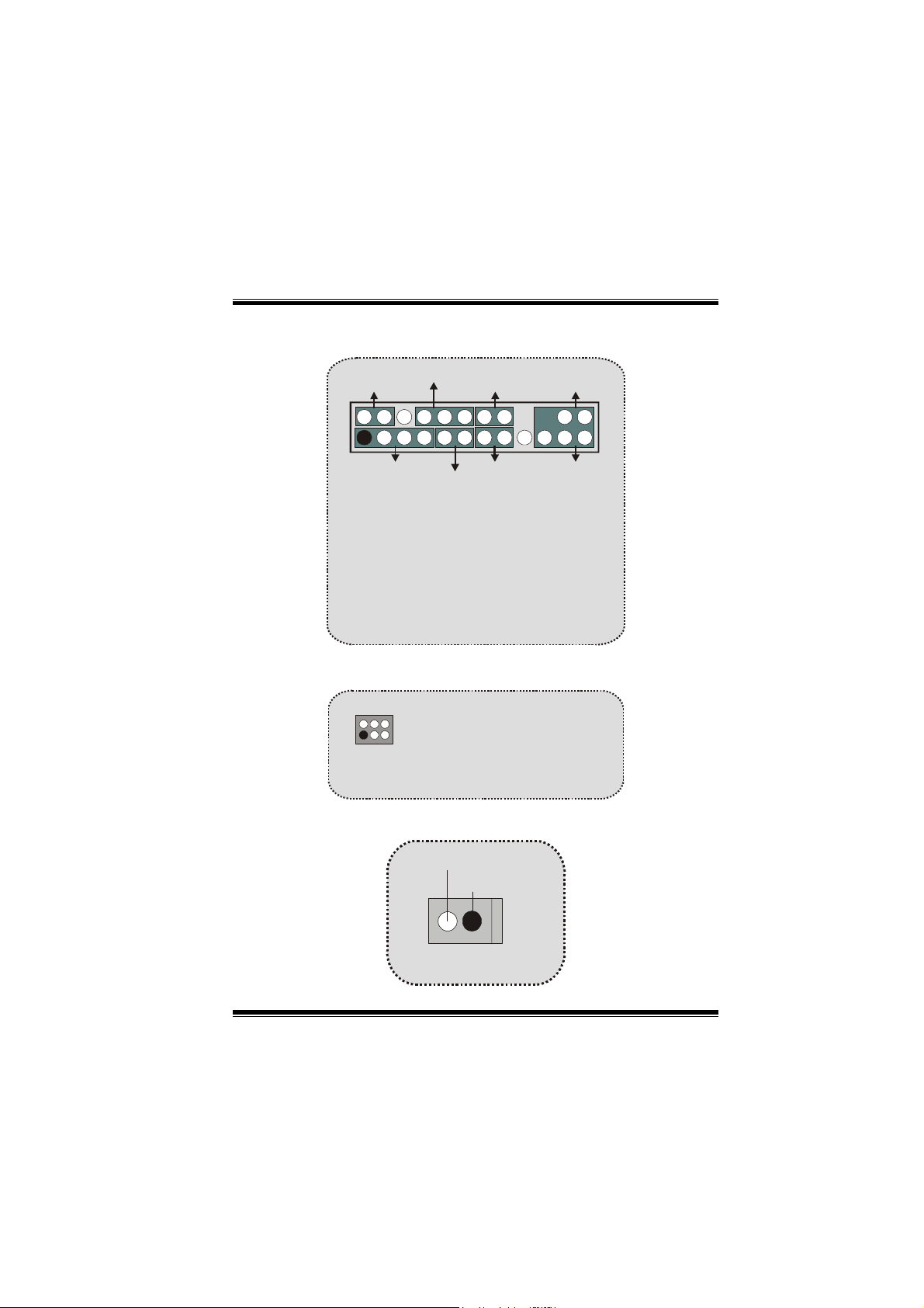
Front Panel Connector: JPANEL1
SLP
2
1
SPK ==> Speaker Conn.
HLED ==> Hard Driver LED
RST ==> Reset Button
IR ==> Infrared Conn.
SLP ==> Sleep Button
PWR_LED ==> Power LED
ON/ OFF ==> Power-on Button
SPK
PWR_LED
(+) (-)(+)
(+) (-)
HLED
RST
CPU Clock Selection: JCLK1
1
JCLK1
Pin 1-2, 5-6 ==> 100 Mhz
64
Pin 2-3, 5-6 ==> 133 Mhz
3
(default)
Pin 2-3, 4-5 ==> 166Mhz
Case Open Connector: JCI1
Case Open Signal
Ground
1
JCI1
p
t
i
o
n
p
t
i
o
n
i
p
t
i
o
n
IRON/OFF
24
23
IR
9
M
o
t
h
e
r
b
o
a
r
d
D
e
s
c
r
i
p
t
i
M
M
o
t
h
e
r
b
o
a
r
d
D
e
o
t
h
e
r
b
o
a
s
r
d
D
e
s
o
c
r
i
p
t
i
o
c
r
i
p
t
i
o
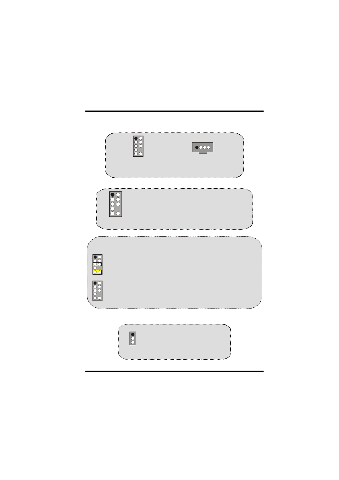
Audio Subsystem: JAUDIO1/ JCDIN1
(Front Audio Header)
(Front Audio Header)
12
2
1
JAUDIO1
JAUDIO1
109
1
JCDIN1
JCDIN1
(CD-ROM Audio-In Header)
(CD-ROM Audio-In Header)
n
n
n
1
12
JAUDIO1
12
910
12
9
10
Pin 5 and 6
==>
Pin 9 and 10
Audio line out and mic in signals are
available for front panel audio connectors.
Pin1 ==> Mic In Pin2 ==> Ground
Pin3 ==> Mic Power Pin4 ==> Audio Power
Pin5 ==> RT Line Out Pin6 ==> RT Line Out
Pin7 ==> Reserved Pin8 ==> KEY
Pin9 ==> LFT Line Out Pin10 ==> LFT Line Out
Front Panel Audio Connector/ Jumper Block
Audio line out signals are routed
to the back panel audio line out connector.
Clear CMOS Jumper: JCMOS1
1
JCMOS1
Pin 1-2 on ==> Normal Operation
(default)
Pin 2-3 on ==> Clear CMOS Data
10
 Loading...