

Page 1

BIPV10-IA Setup Manual
FCC Information and Copyright
This equipment has been tested and found to comply with the limits of a Class
B digital device, pursuant to Part 15 of the FCC Rules. These limits are designed
to provide reasonable protection against harmful interference in a residential
installation. This equipment generates, uses, and can radiate radio frequency
energy and, if not installed and used in accordance with the instructions, may
cause harmful interference to radio communications. There is no guarantee
that interference will not occur in a particular installation.
The vendor makes no representations or warranties with respect to the
contents here and specially disclaims any implied warranties of merchantability
or fitness for any purpose. Further the vendor reserves the right to revise this
publication and to make changes to the contents here without obligation to
notify any party beforehand.
Duplication of this publication, in part or in whole, is not allowed without first
obtaining the vendor’s approval in writing.
The content of this user’s manual is subject to be changed without notice and
we will not be responsible for any mistakes found in this user’s manual. All the
brand and product names are trademarks of their respective companies.
Page 2

Table of Contents
Chapter 1: Introduction ........................................ 3
1.1 Before You Start ................................................................................ 3
1.2 Package Checklist............................................................................. 3
1.3 Mainboard Specification................................................................... 4
1.4 Rear Panel.......................................................................................... 5
1.5 Mainboard Layout ............................................................................ 6
Chapter 2: Installation .......................................... 7
2.1 CPU...................................................................................................... 7
2.2 Fan Header......................................................................................... 7
2.3 System Memory.................................................................................. 8
2.4 Power Supply ..................................................................................... 9
2.5 Onboard Slot/Connector/Header/Jumper .................................... 10
Chapter 3: BIOS Setup ........................................ 21
3.1 Main Menu........................................................................................ 23
3.2 Advanced Menu............................................................................... 26
3.3 PCI/PnP Menu.................................................................................. 37
3.4 Boot Menu........................................................................................ 40
3.5 Chipset Menu.................................................................................... 42
3.6 Exit Me nu.......................................................................................... 47
Chapter 4: Useful Help ........................................ 51
4.1 Driver Installation Note.................................................................. 51
4.2 AMI BIOS Beep Code....................................................................... 52
4.3 Troubleshooting............................................................................... 53
Page 3

BIPV10-IA
3
CHAPTER 1: INTRODUCTION
1.1 B
EFORE YOU START
Thank you for choosing our product. Before you start installing the
mainboard, please make sure you follow the instructions below:
Prepare a dry and stable working environment with
sufficient lighting.
Always disconnect the system from power outlet
before operation.
Before you take the mainboard out from anti-static
bag, ground yourself properly by touching any safely
grounded appliance, or use grounded wrist strap to
remove the static charge.
Avoid touching the components on mainboard or the
rear side of the board unless necessary. Hold the board
on the edge, do not try to bend or flex the board.
Do not leave any unfastened small parts inside the
case after installation. Loose parts will cause short
circuits which may damage the equipment.
Keep the system from dangerous area, such as heat
source, humid air, and water.
Please switch on/off the machine normally. That is, DO
NOT pull out power cord directly from the mainboard
or the system may damage.
1.2 PACKAGE CHECKLIST
Mini-ITX Mainboard x 1
Fully Setup Driver CD x 1
I/O Bracket x 1
SATA Cable x 1 (Optional)
Page 4

Mini-ITX Mainboard Manual
4
1.3 MAINBOARD SPECIFICATION
Sp ecif icat ion
CPU
Int el C PU On - bo ar d
Intel Atom D525 @1.8GHz dual core
Pinev iew-D Process or
Optional for:
D425 @1.8GHz (TWP 10W)
FSB
Supports up 800 MHz
Chipset
Int el NM10 Ex pres s Chips et
Graphic
Intel Pineview-D integrated graphics engine
Max Shared Video Memory is 384 MB
Supports dual displays (Extended mode)
as b elow:
—24bit LVDS (by CH7036)
—RGB (Support up to WXGA+
2048x1536/60Hz)
Super I/O
ITE IT8718 + FINTEK F81216D
Provides the most commonly used legacy
Super I/O functionality.
128pin type
En viron men t C o nt rol in itiat ives ,
H/W Monit or
Fan Speed Controller
Main
Memor y
LONG-DIMM x 2
Supports DDR3 800 MHz
DIMM supports 512MB / 1GB / 2GB
Max Memor y Capacit y 4 GB
Registered DIMM or ECC DIMM is not
supported
SATA
Ch ips et b uilt - in S er ial ATA cont rolle r
SATA Ver sion 2. 0 sp ec ific at ion co mp li an t
Data transfer rates up to 3.0 Gb/s
LAN
Realtek RTL 8111E x 2
10 / 100 / 1000 Mb/s auto negotiation
Ha lf / F u ll dup lex capa bi lit y
Sound
Codec
Realtek ALC662
5.1 channels audio out t (only for x3 audio
jack version)
High- De fin it io n A ud io supp ort
PCI slo t x1
Slot
Mini PCI-E Slot x1
SATA2 Connector x2
Front Panel Header x1
Parallel Connector x1
On Board
Connectors
& Headers
Digital I/O Connector x1
Page 5

BIPV10-IA
5
Sp ecif icat ion
CPU Fan Header x1
System Fan Header x1
Clear C MOS He ader x1
AT/AT X Power Swit ch He ader x1
USB 2.0 Header x2 (Support 3 USB devices)
LVDS Connector x1
LCD Power Select Header x1
LC D B acklight Po wer ON /OFF Header x1
LCD Backlight Inverter Connector x1
Inverter Power Select Header x1
Backlight Brightness Adjust Header x1
Serial Connectors (RS-232) x3
Power Connector (20pin) x 1
Rear Panel
I/O
PS/2 Keybo ard x1
PS/2 Mous e x1
Serial Port x3
VGA Port x1
LAN port x 2
USB Po rt x4
Audio Jack (Line-out/Mic) x2
3 x RS-232
Op tio n al x 3 (Line-in/L ine- out /Mic)
Board Size
170 mm (W) x 170 mm (L) Mini-ITX
OS
Support
Windows XP/XPE, Linux
Biostar reserves the right to add or remove
support for any OS with or without notice.
1.4 R
EAR PANEL
PS/2
Mouse
PS/2
Keyboard
JCOM4
Mic In
(Center/SUB)
Line In
(Rea r)
(Optional)
Line Out
(Fro nt)
LAN
USB 2.0 x 4
JCOM3
LAN
VGA
JCOM1
Page 6

Mini-ITX Mainboard Manual
6
1.5 MAINBOARD LAYOUT
JCOM1
A
B
JKBMS1
JVGA1
JRJ45 USB 1
JRJ45 USB 2
JAUDIO1
JCOM2
JCOM5
JCOM6
JP2
JP1
JP5
JP4
JP3
JP6
LVDS-OUT1
JC1
JLV2
JLV1
JBL1
PE1
PCI1
JPRNT1
JDIO1
JUSB4
BAT1
JUSB3
BIOS
JCMOS1
JAT1
JSFAN1
JPANEL1
SATA1 SATA2
DDR3_A2
DDR3_A1
JATXPWR1
Intel
Atom
D525
CPU 1
NM10
JBL2
JCFAN 1
Note: represents the 1■
st
pin.
Page 7

BIPV10-IA
7
CHAPTER 2: INSTALLATION
2.1 CPU
The mainboard includes an embedded I ntel Atom D525 processor, and a
heatsink has been installed to provide sufficient cooling.
2.2 FAN HEADER
The fan header supports cooling-fans built in the system. The fan cable
and connector may be different due to the fan manufacturer.
JCFAN1: CPU Fan Header
Pin Assignment
1 Ground
2 +12V
3 FAN RPM rate
sense
13
JSFAN1: System Fan Header
Pin Assignment
1 Ground
2 +12V
3 FAN RPM rate
sense
13
Note:
The CPU Fan Header and System Fa n Header support 3-pin head connector. When
connecting with wires onto connectors, please note that the red wire is the positive and
should be co nnected to pin#2, and the black wire is Ground and should be connected to
GND.
Page 8
Mini-ITX Mainboard Manual
8
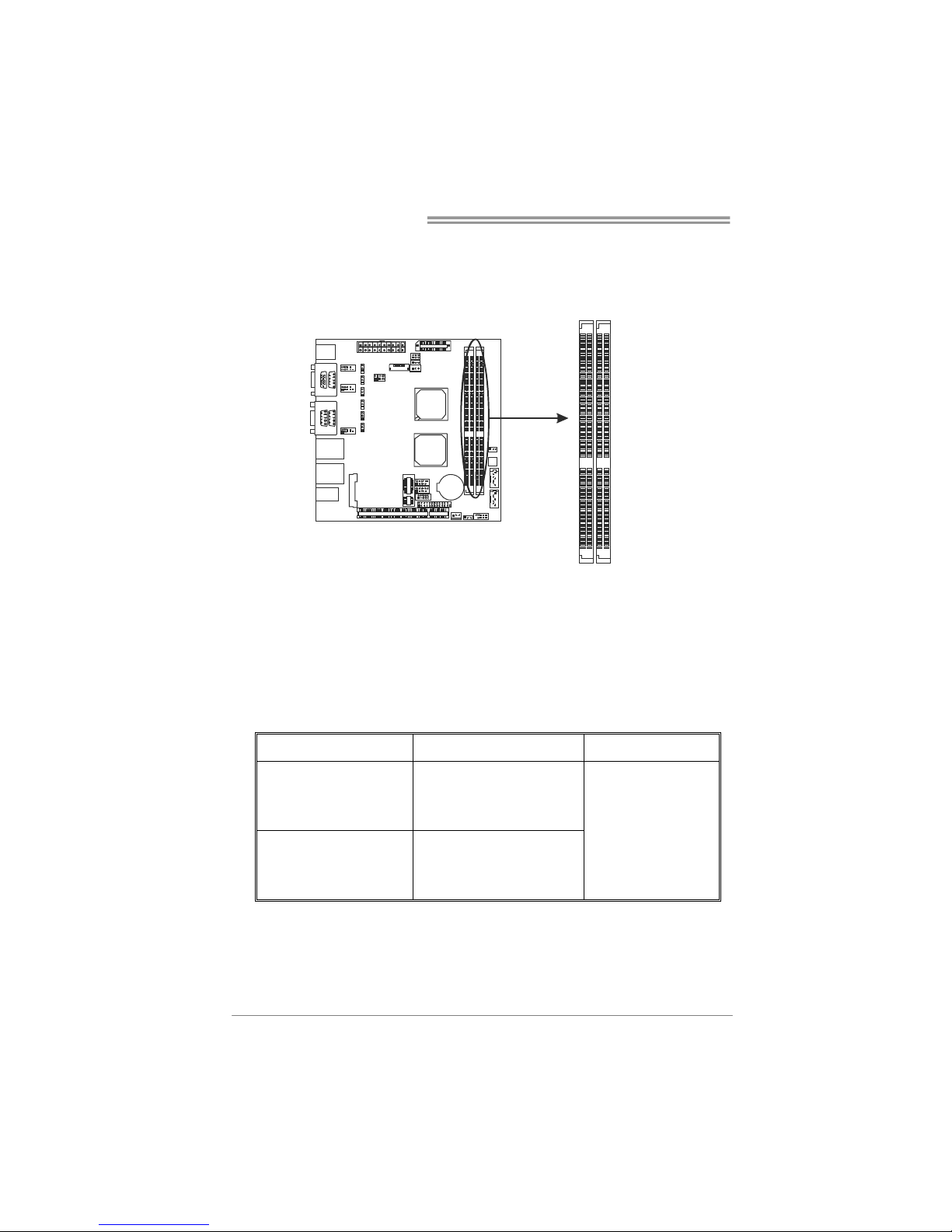
2.3 SYSTEM MEMORY
DDR3_A1/DDR3_A2: Memory Module (LONG-DIMM)
DD R3_A 1
DD R3_A 2
2 Align a DIMM on the slot such that the notch on the DIMM matches the
break on the Slot.
3 Insert the DIMM firmly into the slot until the retaining chip snap back in
place and the DIMM is properly seated.
Memory Capacity
DIMM Socket Location DDR3 Module Total Memory Size
DDR3_A1 512MB/1GB/2GB
DDR3_A2 512MB/1GB/2GB
Max is 4GB.
Page 9

BIPV10-IA
9
2.4 POWER SUPPLY
JATXPWR1: ATX Power Source Connector (20-pin)
This connector allows user to connect 20-pin power connector on the power
supply.
110
1120
Pin Assignment Pin Assignment
1 +3.3V 11 +3.3V
2 +3.3V 12 -12V
3 GND 13 GND
4 +5V 14 Power Supply On
5 GND 15 GND
6 +5V 16 GND
7 GND 17 GND
8 Power Good 18 NC
9 +5V Standby 19 +5V
10 +12V 20 +5V
Page 10

Mini-ITX Mainboard Manual
10
2.5 ONBOARD SLOT/CONNECTOR/HEADER/JUMPER
PCI1: Peripheral Component Inte rconnect Slot
This mainboard is equipped with 1 standard PCI slot. PCI stands for Peripheral
Component Interconnect, and it is a bus standard for expansion cards. This PCI
slot is designated as 32 bits.
PCI1
PE1: Mini PCI-E Slot
This mainboard is equipped with 1 Mini PCI-E Slot.
Page 11

BIPV10-IA
11
SATA1/SATA2: Serial ATA Connectors
These next generation connectors support the thin Serial ATA cable for primary
internal storage devices. T he current Serial ATA interface allows up to 3.0
Gbit/s data transfer rate.
Pin Assignment
1 GND
2 TX+
3 TX-
4 GND
5 RX-
6 RX+
7 GND
1
4
7
SATA2
SATA1
USB1/USB2: USB 2.0 Headers
The mainboard provides 2 front USB pin header, allowing up to 3 additional USB
2.0 ports up to maximum throughput of 480 Mbps. Connect the USB cable into
the pin header for using high-speed USB interface peripherals.
Note: JUSB4 only supports Pin1, 3, 5, 7, so it supports 1 USB device only.
Pin Assignment Pin Assignment
1 +5V (fused) 2 +5V (fused)
3 USB6- 4 USB7-
5 USB6+ 6 USB7+
7 Ground 8 Ground
9 Key 10 NC
1
210
9
JUSB4
JUSB3
Page 12

Mini-ITX Mainboard Manual
12
JPANEL1: Front Panel Header
This 10-pin header includes Power-on, Reset, HDD LED, and Power LED
connection. It allows user to connect the system case’s front panel switch
functions.
91
210
Pin Assignment Function Pin Assignment Function
1 Key N/A 2 Power LED+
3 HD LED+ 4 Power LED+
5 HD LED-
HDD LED
6 Power LED-
Power LED
7 Reset GND 8 Power
9 Reset
Reset Button
10 Power GND
Power Button
JDIO1: Digital I/O Connector
This connector offers 4-pair of digital I/O functions and address is set in BIOS.
The default address is: A21H: Output bit0~3; A22H: Input bit0~3.
Pin Assignment
1 5V
2 Digital-In-30
3 Digital-Out-20
4 Digital-In-31
5 Digital-Out-21
6 Digital-In-32
7 Digital-Out-22
8 Digital-In-33
9 Digital-Out-23
1
2910
10 GND
Page 13

BIPV10-IA
13
JCOM1 / JCOM3 / JCOM4: Serial port Connectors
The motherboard has 3 Serial Port Connectors for connecting RS-232 Port.
Pin
Assignment
1 Carrier detect (DCD)
2 Received data (RXD)
3 Transmitted data (TXD)
4 Data terminal ready (DTR)
5 Signal ground (GND)
6 Data set ready (DSR)
7 Request to send (RTS)
8 Clear to send (CTS)
JCOM3
JCOM4
JCOM1
9 Ring or 5V
* Do not support RI wake up
JCOM2/JCOM5/JCOM6: Serial Port Connectors
The motherboard has 3 Serial Port Connectors for connecting RS-232 Port.
Pin
Assignment
1 -PDCD
2 PSIN
3 PSOUT data
4 -PDTR
5 GND
6 -PDSR
7 -PRTS
8 -PCTS
9 -PRI
19
210
JCOM2
JCOM5
JCOM6
10 5V or 12V
Page 14
Mini-ITX Mainboard Manual
14
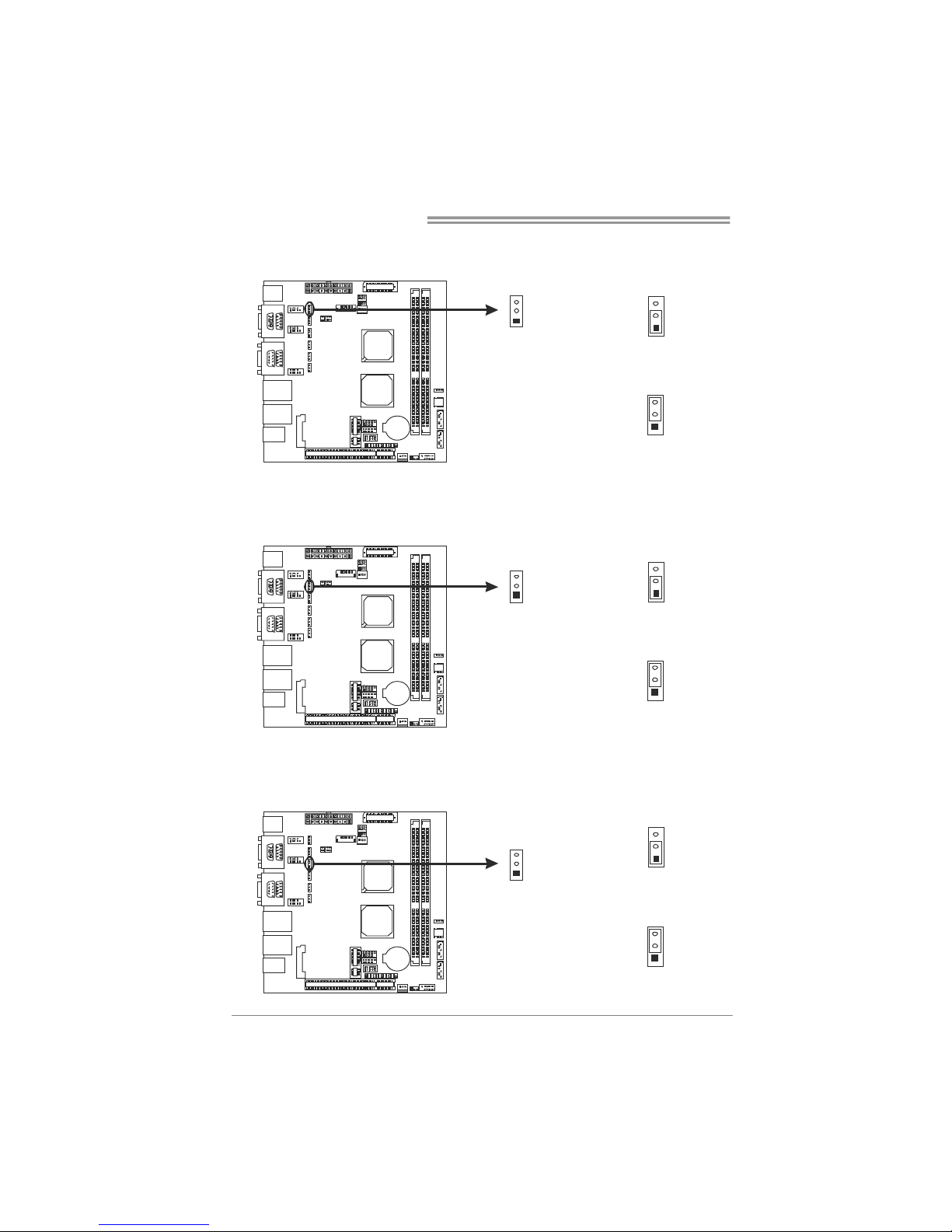
JP2: Voltage Switch Header for JCOM2
This header is for controlling the Pin10 of JCOM2 to switch 5V or 12V.
1
3
Pin 1-2 Close:
Pin10=5V
3
1
1
3
Pin 2-3 Close:
Pin10=12V (Default)
JP1: Voltage Switch Header for JCOM1
This header is for controlling the Pin9 of JCOM1 to switch Ring or 5V.
1
3
Pin 1-2 Close:
Pin9=5V
3
1
1
3
Pin 2-3 Close:
Pin9=Ring (Default)
JP5: Voltage Switch Header for JCOM5
This header is for controlling the Pin10 of JCOM5 to switch 5V or 12V.
1
3
Pin 1-2 Close:
Pin10=5V
3
1
1
3
Pin 2-3 Close:
Pin10=12V (Default)
Page 15

BIPV10-IA
15
JP4: Voltage Switch Header for JCOM4
This header is for controlling the Pin9 of JCOM4 to switch Ring or 5V.
1
3
Pin 1-2 Close:
Pin9=5V
3
1
1
3
Pin 2-3 Close:
Pin9=Ring (Default)
JP3: Voltage Switch Header for JCOM3
This header is for controlling the Pin9 of JCOM3 to switch Ring or 5V.
1
3
Pin 1-2 Close:
Pin9=5V
3
1
1
3
Pin 2-3 Close:
Pin9=Ring (Default)
JP6: Voltage Switch Header for JCOM6
This header is for controlling the Pin10 of JCOM6 to switch 5V or 12V.
1
3
Pin 1-2 Close:
Pin10=5V
3
1
1
3
Pin 2-3 Close:
Pin10=12V (Default)
Page 16
Mini-ITX Mainboard Manual
16
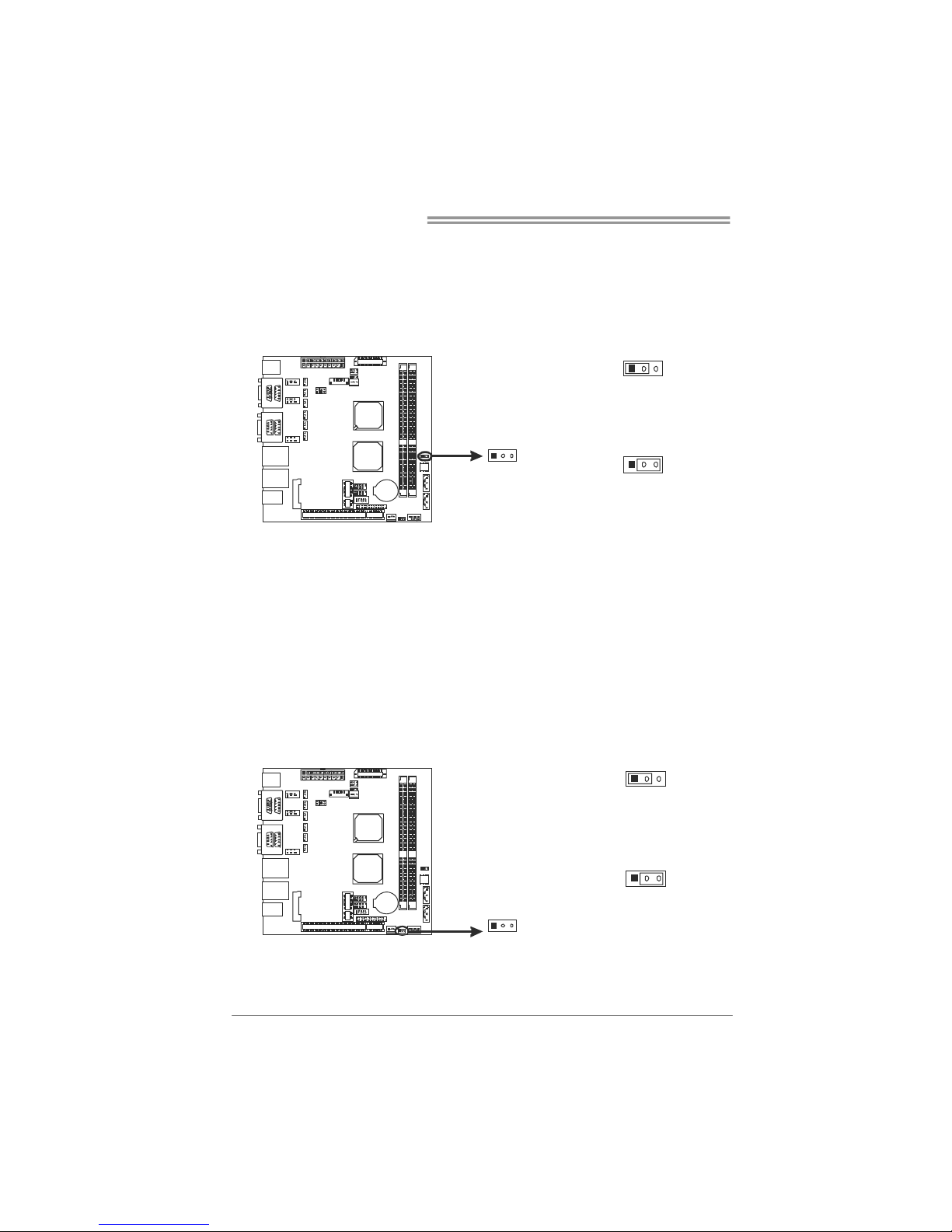
JCMOS1: Clear CMOS Header *
Placing the jumper on pin2-3 allows user to restore the BIOS safe setting and
the CMOS data. Please carefully follow the procedures to avoid damaging the
mainboard.
31
Pin 1-2 Close: (Default)
Normal Operation.
13
3
1
Pin 2-3 Close:
Clear CMOS data.
Clear CMOS Procedures:※
1. Remove AC power line.
2. Set the jumper to “Pin 2-3 close”.
3. Wait for five seconds.
4. Set the jumper to “Pin 1-2 close”.
5. Power on the AC.
6. Reset your desired password or clear the CMOS data.
JAT1: AT/ATX Power Switch Header *
This header is for switching between AT and ATX power.
31
Pin 1-2 Close:
For AT Power
1
3
3
1
Pin 2-3 Close: (Default)
F or ATX Power
Page 17

BIPV10-IA
17
LVDS-CONN1: LVDS Connector
This connector is for devices requiring display interface such as LVDS.
This connector supports 18/24 bit single-channel panels up to 1366 x 768
It is strongly recommended to use the matching JOY DAY INDUSTRIAL -
A1252WV-SF-2X20PD01 connector.
2
1
40
39
Pin Assignment Pin Assignment
1 NC 2 PVDD (+3.3V or +5V or +12V)
3 NC 4 PVDD (+3.3V or +5V or +12V)
5 GND 6 GND
7 NC 8 GND
9 NC 10 LVDS1_TX0- (Differential signal)
11 GND 12 LVDS1_TX0+ (Differential signal)
13 NC 14 GND
15 NC 16 LVDS1_TX1- ( (Differential signal)
17 GND 18 LVDS1_TX1+ (Differential signal)
19 NC 20 GND
21 NC 22 LVDS1_TX2- (Differential signal)
23 GND 24 LVDS1_TX2+(Differential signal)
25 NC 26 GND
27 NC 28 LVDS1_CLK- (Differential signal)
29 +5V 30 LVDS1_CLK+(Differential signal)
31 I2C_CLK 32 GND
33 +3.3V 34 LVDS1_TX3-(Differential signal)
35 NC 36 LVDS1_TX3+(Differential signal)
37 PVDD (+3.3V or +5V or +12V) 38 GND
39 PVDD (+3.3V or +5V or +12V) 40 I2C_DATA
Page 18

Mini-ITX Mainboard Manual
18
JLV2: LCD Power Select Header *
This header allows you to select LCD Power.
2
1
Pin 1-2 Close:
PVDD=3.3V (Default)
4
3
Pin 2-3 Close:
PVDD=5V
51
6
2
6
5
Pin 2-3 Close:
PVDD=12V
JLV1: LCD Backlight Inverter Power Select Header *
This header is for selecting LCD Backlight Inverter Power.
31
Pin 1-2 Close:
Inverter Power=5V
31
3
1
Pin 2-3 Close:
Inverter Power=12V
(Default)
JBL1: LCD Backlight Power ON/OFF Header *
This header allows you to control the LCD Backlight Power ON/OFF.
1
Header Clo se:
Backlight Po wer OF F
2
1
1
Header Open:
Backlight Po wer ON
Page 19

BIPV10-IA
19
JBL2: LCD Backlight Brightness Adjust Header *
This header is for adjusting LCD backlight brightness.
24
13
Short Pin 1-2:
Increase Brightness
123
4
24
13
Short Pin 3-4:
Decrease Brightness
JC1: LCD Backlight Inverter Connector
This connector is for connecting to LCD for providing backlight control function.
It is strongly recommended to use the matching JOY DAY INDUSTRIAL
- A1250WV-S-8P connector.
Pin Assignment
1 5V/12V DC
2 5V/12V DC
3 NC
4 NC
5 Backlight On
6 Brightness Adjust
7 GND
8 GND
Page 20

Mini-ITX Mainboard Manual
20
JPRNT1: Printer Port Connecto r
This header allows you to connect printer port on the PC.
1
25
2
26
Pin Assignment Pin Assignment
1 -Strobe 14 Ground
2 -ALF 15 Data 6
3 Data 0 16 Ground
4 -Error 17 Data 7
5 Data 1 18 Ground
6 -Init 19 -ACK
7 Data 2 20 Ground
8 -Scltin 21 Busy
9 Data 3 22 Ground
10 Ground 23 PE
11 Data 4 24 Ground
12 Ground 25 SCLT
13 Data 5 26 Key
*How to Setup Jumpers
The illustration shows how to set up jumpers. When the jumper cap is placed on
pins, the jumper is “close”, if not, that means the jumper is “open”.
Pin opened Pin closed Pin1-2 closed
Page 21

BIPV10-IA
21
CHAPTER 3: BIOS SETUP
Introduction
The purpose of this chapter is to describe the settings in the AMI BIOS Setup
program on this motherboard. The Setup program allows users to modify the basic
system configuration and save these settings to CMOS RAM. The power of CMOS
RAM is supplied by a battery so that it retains the Setup information when the
power is turned off.
Basic Input-Output System (BIOS) determines what a computer can do without
accessing programs from a disk. This system controls most of the input and output
devices such as keyboard, mouse, serial ports and disk drives. BIOS activates at the
first stage of the booting process, loading and executing the operating system. Some
additional features, such as virus and password protection or chipset fine-tuning
options are also included in BIOS.
The rest of this manual will to guide you through the options and settings in BIOS
Setup.
Plug and Play Support
This AMI BIOS supports the Plug and Play Version 1.0A specification.
EPA Green PC Support
This AMI BIOS supports Version 1.03 of the EPA Green PC specification.
ACPI Support
AMI ACPI BIOS support Version 1.0/2.0 of Advanced Configuration and Power
interface specification (ACPI). It provides ASL code for power management and
device configuration capabilities as defined in the ACPI specification, developed by
Microsoft, Intel and Toshiba.
Page 22

Mini-ITX Mainboard Manual
22
PCI Bus Support
This AMI BIOS also supports Version 2.3 of the Intel PCI (Peripheral Component
Interconnect) local bus specification.
DRAM Support
DDR2 SDRAM (Double Data Rate II Synchronous DRAM) is supported.
Supported CPUs
This AMI BIOS supports the Intel CPU.
Using Setup
When starting up the computer, press <Del>
during the Power-On Self-Test (POST) to enter
the BIOS setup utility.
In the BIOS setup utility, you will see General
Help description at the top right corner, and this
is providing a brief description of the selected
item. Navigation Keys for that particular
menu are at the bottom ri ght corner, and you can
use these keys to select item and change the
settings.
Notice
z The default BIOS settings apply for most conditions to ensure optimum
performance of the motherboard. If the system becomes unstable after
changing any setti ngs, please load the default setti ngs to ensure system’s
compatibility and stability. Use Load Setup Default under the Exit Menu.
z For better system performance, the BIOS firmware is being continuously updated.
The BIOS information described in this manual is for your reference only.
The actual BIOS information and settings on board may be slightly different
from this manual.
z The content of this manual is subject to be changed without notice. We will not
be responsible for any mistakes found in this user’s manual and any system
damage that may be caused by wrong-settings.
General Help
Navigation Keys
Page 23

BIPV10-IA
23
3.1 MAIN MENU
Once you enter AMI BIOS Setup Utility, the Main Menu will appear on the screen
providing an overview of the basic system information.
BIOS S ETUP UTIL IT
Y
Main Advan ced PCIPnP Boot Chipset
vxx.xx (C)Copyr ight 1985 -200x, Am erican Megatrends, Inc.
Select Sc reen
Select It em
Change Fi eld
Select Fi eld
General H elp
Save and Exit
Exit
+Tab
F1
F10
ESC
Use [ENT ER], [TAB ]
or [SHIFT-TA B] to
select a field.
Use [+] or [-] to
configur e system Time.
System O verview
AMI BIOS
System M emory
[ : 00:00]
System D ate [Fri 01 /01/2010]
> IDE Co nfigurati on
Version :01.01. 01
Build Da te:01/01/ 10
Size :
System T ime 00
Exit
AMI BIOS
Shows system information including BIOS version, built date, etc.
System Memory
Shows system memory size, VGA s hard memor y will be excluded..
System Time
Set the system internal clock.
System Date
Set the sys te m date. Note that the ‘Da y’ auto mati cally changes w hen you set the
date.
Page 24

Mini-ITX Mainboard Manual
24
IDE Configuration
The BIOS will automatically detect the presence of IDE/SATA devices. There is a
sub-menu for each IDE/SATA device. Select a device and press <Enter> to enter
the sub-menu of detailed options.
BIOS S ETUP UTIL IT
Y
Main
vxx.xx (C)Copyr ight 1985 -200x, Am erican Megatrends, Inc.
Select Sc reen
Select It em
Go to Sub Screen
General H elp
Save and Exit
Exit
Enter
F1
F10
ESC
IDE Confugura tion
> SATA 1
> SATA 2
Hard Dis k Write P rotect [Disabl ed]
IDE Dete ct Time O ut (Sec) [35]
Configur e SATA as [IDE]
O ptions
IDE
AHCI
Disabled
Configure SATA as
This item allows you to determine the control mode of SATA.
Optio ns: IDE (De fault) / AHCI / Disabled
SATA 1/2 Devices
BIOS S ETUP UTIL IT
Y
Main
vxx.xx (C)Copyr ight 1985 -200x, Am erican Megatrends, Inc.
Select Sc reen
Select It em
Change Op tion
General H elp
Save and Exit
Exit
+F1
F10
ESC
Select t he type
of device connect ed
to the system.
SATA 1 D evice
LBA/Larg e Mode [Auto]
Block (M ulti-Sect or Transfe r)[Auto]
PIO Mode [Auto]
DMA Mode [Auto]
S.M.A.R. T [Auto]
32Bit Da ta Transf er [Enable d]
Device :
Type [Auto]
Page 25

BIPV10-IA
25
The BIOS detects the information and values of respective devices, and these
information and values are shown below to the name of the sub-menu.
Type
Select the type of the SATA drive.
Options: Auto (Default) / CD/DVD / ARMD / Not Installed
LBA/Large Mode
Enable or disable the LBA mode.
Optio ns: Auto (Default) / Disabled
Block (Multi-Sector Transfer)
Enable or disable multi-sector transfer.
Optio ns: Auto (Default) / Disabled
PIO Mode
Select the PIO mode.
Options: Auto (Default) / 0 / 1 / 2 / 3 / 4
DMA Mode
Select the DMA mode.
Optio ns: Auto (Default) / SWDMA0 ~ S WDMA2 / MWDMA0 ~ MWDMA2 /
UDMA0 ~ UDMA5
S.M.A.R.T
Set the Smart Monitoring, Analysis, and Reporting Technology.
Optio ns: Auto (Default) / Disabl ed / Enabled
32Bit Data Transfer
Enable or disable 32-bit data transfer.
Options: Enabled (Default) / Disabled
Hard Disk Write Protect
Disable or enable device write protection. This will be effective only if the device
is accessed through BIOS.
Options: Disabled (Default) / Enabled
IDE Detect Time Out (Sec)
Select the time out value for detecting IDE/SATA devices.
Options: 35 (Default) / 30 / 25 / 20 / 15 / 10 / 5 / 0
Page 26

Mini-ITX Mainboard Manual
26
3.2 ADVANCED MENU
The Advanced Menu allows you to configure the settings of CPU, Super I/O, Power
Management, and other system devices.
Notice
z Beware of that setting inappropriate values in items of this menu may cause
system to malfunction.
BIOS S ETUP UTIL IT
Y
Main Advanced
PCIPnP Boot
Chipset
vxx.xx (C)Copyr ight 1985 -200x, Am erican Me gatrends, Inc.
Select Sc reen
Select It em
Go to Sub Screen
General H elp
Save and Exit
Exit
Enter
F1
F10
ESC
Configur e CPU.Advanced Settings
WARNING: Setting wrong valu es in bel ow sectio ns
may caus e system t o malfunc tion.
> USB Co nfigurati on
> SuperI O Configu ration
> Hardwa re Health Configura tion
> Smart Fan Confi guration
> ACPI C onfigurat ion
> CPU Co nfigurati on
Exit
CPU Configuration
This item shows the CPU information that the BIOS automatically detects.
BIOS S ETUP UTIL IT
Y
Advan ced
vxx.xx (C)Copyr ight 1985 -200x, Am erican Me gatrends, Inc.
Select Sc reen
Select It em
Change Op tion
General H elp
Save and Exit
Exit
+F1
F10
ESC
Disabled for Wind owsXP
Configur e advance d CPU sett ings
Module V ersion:3F .1C
Manufact urer:Inte l
Frequenc y :
FSB Spee d :
Cache L1 :
Cache L2 :
Ratio Ac tual Valu e:
Max CPUI D Value L imit [Disab led]
Execute- Disable B it Capabil ity[Enabl ed]
Hyper Th reading T echnology [Enabl ed]
Page 27

BIPV10-IA
27
Max CPUID Value Limit
When the computer is booted up, the operating system executes the CPUID
instruction to identify the processor and its capabilities. Before it can do so, it must
first query the processor to find out the highest input value CPUID recognizes. This
determines the kind of basic information CPUID can provide the operating system.
Options: Disabled (Default) / Enabled
Execute-Disable Bit Capability
This item all ows yo u to co nfi gure the Exec ute Disabl ed Bit f uncti o n, whic h protec ts
your system from buffer overflow attacks.
Options: Enabled (Default) / Disabled
Hyper Threading Technology
Enabled for Windows XP and Linux (OS optimized for Hyper Threading
Technology) and disabled for other OS (OS not optimized for Hyper Threading
Technology).
Options: Enabled (Default) / Disabled
SuperIO Configuration
BIOS S ETUP UTIL IT
Y
Advan ced
vxx.xx (C)Copyr ight 1985 -200x, Am erican Me gatrends, Inc.
Select Sc reen
Select It em
Change Op tion
General H elp
Save and Exit
Exit
+F1
F10
ESC
Allows B IOS to Se lect
Serial P ort1 Base
Addresse s.
Configur e ITE8718 Super IO Chipset
Serial P ort1 Addr ess [3F8/I RQ4]
Second I O UART IR Q MODE [PCI I RQ Sharin g]
Serial P ort2 Addr ess [2F8/I RQ3]
Parallel Port Add ress [378]
Parall el Port M ode [Norma l]
Parall el Port I RQ [IRQ7]
Serial P ort 3-6 I RQ Share [IRQ5]
Serial P ort3 Addr ess [3E8]
Serial P ort4 Addr ess [2E8]
Serial P ort5 Addr ess [2F0]
Serial P ort6 Addr ess [2E0]
Watch Do g Degree [Secon d]
Watch Do g Timer [00000 ]
Serial Port1 Address
Select an address and corresponding interrupt for Serial Port 1.
Options: 3F8/IRQ4 (Default) / 3E8/IRQ4 / 2E8/IRQ3 / Disabled
Page 28

Mini-ITX Mainboard Manual
28
Serial Port2 Address
Select an address and corresponding interrupt for Serial Port 2.
Options: 2F8/IRQ3 (Default) / 3E8/IRQ4 / 2E8/IRQ3 / Disabled
Parallel Port Address
This item allows you to determine access onboard parallel port controller with
which I/O Address.
Options: 378 (Default) / 278 / 3BC / Disabled
Parallel Port Mode
This item allows you to determine how the parallel port should function.
Options: Normal (Default) Using Parallel port as Standard Printer Port.
EPP Using Parallel Port as Enhanced Parallel Port.
ECP Using Parallel port as Extended Capabilities Port.
ECP+EPP Usi ng Parallel port as ECP & EPP mode.
ECP Mode DMA Channel
This item allows you to select parallel port ECP DMA.
Optio ns: DMA3 (Default) / DMA0 / DMA1
Parallel Port IRQ
This item allows you to select the IRQ for the onboard parallel port.
Optio ns: IRQ7 (De fault) / IRQ5
Second IO UART IRQ MOde
PCI IRQ Sharing for OS (EX. WinXP); ISA IRQ Shari ng for Dos.
Optio ns: PCI IRQ Sharing (Default) / ISA IRQ
Serial Port 3-6 IRQ Share
This item allows you to determine whether Serial Port 3-6 share IRQ.
Optio ns: IRQ5 (Default) / Disabled / IRQ3 / IR Q4 / IRQ7 / IRQ9 / IRQ10 / IRQ11 /
IRQ12
Page 29

BIPV10-IA
29
Serial Port3 Address
This item allows you to select the address of Serial Port3.
Options: 3E8 (Default) / 2E8 / 2F0 / 2E0
Serial Port3 IRQ
This item allows you to select IRQ of Serial Port3.
Options: IRQ5 (Default) / IRQ3 / IRQ4 / IRQ7 / IRQ9 / IRQ10 / IRQ11 / IRQ12
Serial Port4 Address
This item allows you to select the address of Serial Port4.
Options: 2E8 (Default) / 3E8 / 2F0 / 2E0
Serial Port4 IRQ
This item allows you to select IRQ of Serial Port4.
Options: IRQ5 (Default) / IRQ3 / IRQ4 / IRQ7 / IRQ9 / IRQ10 / IRQ11 / IRQ12
Serial Port5 Address
This item allows you to select the address of Serial Port5.
Options: 2F0 (Default) / 3E8 / 2E8 / 2E0
Serial Port5 IRQ
This item allows you to select IRQ of Serial Port5.
Options: IRQ5 (Default) / IRQ3 / IRQ4 / IRQ7 / IRQ9 / IRQ10 / IRQ11 / IRQ12
Serial Port6 Address
This item allows you to select the address of Serial Port6.
Options: 2E0 (Default) / 3E8 / 2E8 / 2F0
Serial Port6 IRQ
This item allows you to select IRQ of Serial Port6.
Options: IRQ5 (Default) / IRQ3 / IRQ4 / IRQ7 / IRQ9 / IRQ10 / IRQ11 / IRQ12
Page 30

Mini-ITX Mainboard Manual
30
Watch Dog Degree
This item allow s you to d eter mi ne the functio na l de gree of Wa tch Do g.
Options: Second (Default) / Minute
Watch Dog Timer
Options: 0 for disabled (Default) / Min=1, Max=65536
Hardware Health Configuration
This item shows the system temperature, fan speed, and voltage information.
Advan ced
Hardware Health C onfigurati on
H/W Heal th Functi on [Enable d]
Shutdown Temperat ure [Disabl ed]
CPU Temperatu re
SYSTEM T emperatur e
JSFan1 S peed
CPU VCore
SB Volta ge
+3.30V
+5.00V
+12.0V
GMCH VCo re
Memory V oltage
BIOS S ETUP UTIL IT
Y
vxx.xx (C)Copyr ight 1985 -200x, Am erican Me gatrends, Inc.
Select Sc reen
Select It em
Change Op tion
General H elp
Save and Exit
Exit
+F1
F10
ESC
Enables Hard ware
Health M onitoring
Device.
H/W Health Function
If with a monitoring system, PC will show PC health status during POST stage.
Options: Enabled (Default) / Disabled
Shutdown Temperature Function
This item allows you to set up the CPU shutdown Temperature. This item is only
effective under Windows 98 ACPI mode.
Options: Disabled (Default) / 60℃/140℉ / 65℃/149℉ / 70℃/158℉ / 75℃/167℉
/ 80℃/176℉ / 85℃/185℉ / 90℃/194℉
Page 31

BIPV10-IA
31
Smart Fan Configuration
BIOS S ETUP UTIL IT
Y
Advan ced
vxx.xx (C)Copyr ight 1985 -200x, Am erican Me gatrends, Inc.
Select Sc reen
Select It em
Change Op tion
General H elp
Save and Exit
Exit
+F1
F10
ESC
When you choice [ Auto]
,[3Pin] or [4Pin] ,
please r un the
calibrat ion to define
the Fan parameter s for
Smart Fa n control
Smart Fa n Configu ration
JSFAN1 S mart Fan [Disabl ed]
Smart Fa n Calibra tion
Control Mode
Fan Ctrl OFF( C)
o
Fan Ctrl On( C)
Fan Ctrl Start va lue
Fan Ctrl Sensitiv e
o
JSFAN1 Smart Fan
This item allows you to control the JSFAN1 Smart Fan function.
Options: Disabled (Default) / Auto
Smart Fan Calibration
Choose this item and then the BIOS will auto test and detect the CPU fan functions
and show CPU fan speed.
Control Mode
This item provides several operation modes of the fan.
Options: Manual (Default) / Quiet / Performance
Fan Ctrl OFF(℃)
If the CPU Temperature is lower than the set value, the fan will turn off.
Options: 0~127 (℃) (With the interval of 1℃)
Fan Ctrl On(℃)
CPU fan s tarts to work when the temperature arrives this set value.
Options: 0~127 (℃) (With the interval of 1℃)
Page 32

Mini-ITX Mainboard Manual
32
Fan Ctrl Start Value
When CPU temperature arrives to the set value, the CPU/System fan will work
under Smart Fan Function mode.
Options: 0~127 (With the interval of 1)
Fan Ctrl Sensitive
Increasing the value of slope PWM will raise the speed of CPU fan.
Options: 0~127 (With the interval of 1)
ACPI Configuration
BIOS S ETUP UTIL IT
Y
Advan ced
vxx.xx (C)Copyr ight 1985 -200x, Am erican Me gatrends, Inc.
Select Sc reen
Select It em
Change Op tion
General H elp
Save and Exit
Exit
+F1
F10
ESC
ACPI Sett ings
Power Supply E mulate Mo de: [ ]ATX
> Advance d ACPI Co nfigurati on
> Chipset ACPI Con figuratio n
Resume On RTC Alar m [Disa bled]
Resume On PME# [Disa bled]
Restore o n AC Powe r Loss by IO [Powr e Off]
Advanced ACPI
Configur ation set tings
Use this section to
configur e additio nal
ACPI opt ions.
Page 33

BIPV10-IA
33
Advanced ACPI Configuration
BIO S SET UP UTILI TY
Adv anced
vxx. xx ( C)Copyri ght 1 985-2 00x, Am erica n Meg atrends , Inc .
Selec t Scree n
Selec t Item
Chang e Optio n
Gener al He lp
Save an d Exit
Exit
+F1
F10
ESC
Advan ced A CPI Con figur ation
ACPI Versi on Feat ures [AC PI v1 .0]
ACPI APIC support [En abled ]
Headl ess m ode [Di sable d]
AMI O EMB t able [En abled ]
Enabl e RSD P pointe rs
to 64-bi t Fixed System
Descr iptio n Tables .
ACPI ver sion ha s some
ACPI Version Features
The item allows you to select the version of ACPI.
Options: ACPI v1.0 (Default) / ACPI v2.0 / ACPI v3.0
ACPI APIC support
This item is used to enable or disable the motherboard's APIC (Advanced
Programmable Interrupt Controller). The APIC provides multiprocessor support,
more IRQs and faster interrupt handling.
Options: Enabled (Default) / Disabled
AMI OEMB table
Set this val ue to allow the ACP I BIOS to add a poi nter to an OEMB table in the
Root System Description Table (RSDT) table.
Options: Enabled (Default) / Disabled
Headless mode
This is a server-specific feature. A headless server is one that operates without a
keyboard, monitor or mouse. To run in headless mode, both BIOS and operating
system (e.g. Windows Server 2003) must support headless operation.
Options: Disabled (Default) / Enabled
Page 34

Mini-ITX Mainboard Manual
34
Chipset ACPI Configuration
BIOS S ETUP UTIL IT
Y
Advan ced
vxx.xx (C)Copyr ight 1985 -200x, Am erican Me gatrends, Inc.
Select Sc reen
Select It em
Change Op tion
General H elp
Save and Exit
Exit
+F1
F10
ESC
South Br idge ACPI Configura tion
Energy L ake Featu re [Dis abled]
APIC ACP I SCI IRQ [Disa bled]
High Per formance Event Time r [Disa bled]
HPET Mem ory Addre ss [FED0 0000h]
Energy Lake Feature
This item allows you to enable or disable the Energy Lake technology feature.
Options: Disabled (Default) / Enabled
APIC ACPI SCI IRQ support
This item is used to set APIC ACPI SCI by IRQ.
Options: Disabled (Default) / Enabled
High Performance Event Timer
This item allows you to enable or disabled the HPET.
Options: Enabled (Default) / Disabled
HPET Memory Address
Options: FED00000h (Default) / FED01000h / FED02000h / FED03000h
Resume On RTC Alarm
When “Enabled”, you can set the date and time at which the RTC (real-time clock)
alarm awakens the system from Suspend mode.
Options: Disabled (Default) / Enabled
RTC Alarm Date (Days)
You can choose which date the system will boot up.
Page 35

BIPV10-IA
35
RTC Alarm Time
You can choose the system boot up time, input hour, minute and second to specify.
Resume On PME#
This item allows you to disable or enable PME to generate a wake event.
Options: Disabled (Default) / Enabled
Restore on AC Power Loss by IO
This setting specifies how your system should behave after a power fail or interrupts
occurs. By choosing Disabled will leave the computer in the power off state.
Choosing Enabled will restore the system to the status before power failure or
interrupt occurs.
Options: Power Off (Default) / Power ON / Last State
USB Configuration
This item shows the USB controller and using USB device information.
BIOS S ETUP UTIL IT
Y
Advan ced
vxx.xx (C)Copyr ight 1985 -200x, Am erican Me gatrends, Inc.
Select Sc reen
Select It em
Change Op tion
General H elp
Save and Exit
Exit
+F1
F10
ESC
Enables supp ort for
legacy U SB. AUTO
option d isables
legacy s upport if
no USB d evices ar e
connecte d.
USB Configura tion
USB Devices Enabl ed:
Module V ersion - 2.24.5-14. 4
Legacy U SB Suppor t [Enable d]
USB 2.0 Controlle r Mode [HiSpee d]
BIOS EHC I Hand-Of f [Enable d]
> USB Ma ss Storag e Device C onfigurat ion
Legacy USB Support
This item determines if the BIOS should provide legacy support for USB devices
like the keyboard, mouse, and USB drive. This feature is useful for using USB
devices with operating systems that do not natively support USB (e.g. Microsoft
MS-DOS or Windows NT).
Options: Enabled (Default) / Disabled / Auto
Page 36

Mini-ITX Mainboard Manual
36
USB 2.0 Controller Mode
This item allows you to select the operation mode of the USB 2.0 controller.
Options: HiSpeed (Default) USB 2.0-480Mbps
FullSpeed USB 1.1-12Mbps
BIOS EHCI Hand-Off
This item allows you to enable support for operating systems without an EHCI
hand- off fea ture .
Options: Enabled (Default) / Disabled
USB Mass Storage Device Configuration
BIOS SET UP UTILITY
Advanced
vxx.xx ( C)Copyright 1985- 200x, American Megatrends, Inc.
Select Sc reen
Select It em
Change Op tion
General H elp
Save and Exit
Exit
+F1
F10
ESC
Number o f seconds
POST waits for the
USB m ass storage
device a fter start
unit command.
USB Mass Storage Device Co nfiguration
USB Mass Storage Reset Delay [20 Sec]
Emulat ion Type [Auto]
Device #
USB Mass Storage Reset Delay
This item allows you to set the reset delay for USB mass storage device.
Options: 20 Sec (Default) / 10 Sec / 30 Sec / 40 Sec
Emulation Type
This item allows you to select the emulation type of the USB mass storage device.
Options: Auto (Default) / Floppy / Forced FDD / Hard Disk / CDROM
Page 37

BIPV10-IA
37
3.3 PCI/PNP MENU
This section describes configuring the PCI bus system. PCI, or Personal Computer
Interconnect, is a system which allows I/O devices to operate at speeds nearing the
speed of the CPU itself uses when communicating with its own special components.
Notice
z Beware of that setting inappropriate values in items of this menu may cause
system to malfunction.
BIOS S ETUP UTIL ITY
Main Advan ced PCIPnP Boot Chipset
vxx.xx (C)Copyr ight 1985 -200x, Am erican Megatrends, Inc.
Select Sc reen
Select It em
Change Op tion
General H elp
Save and Exit
Exit
+F1
F10
ESC
Clear NV RAM durin g
System B oot.
Advanced PCI/PnP Settings
WARNING: Setting wrong valu es in bel ow sections
may caus e system t o malfunc tion.
Plug & P lay O/S [No]
PCI Late ncy Timer [64]
Allocate IRQ to P CI VGA [Yes]
Palette Snooping [Disabl ed]
PCI IDE BusMaster [Enable d]
OffBoard PCI/ISA IDE Card [Auto]
> PCI Re source
Clear NV RAM [No]
Exit
Clear NVRAM
This item allows you to clear the data in the NVRAM (CMOS) by selecting “Yes”.
Optio ns: No (Default) / Yes
Plug & Play OS
When set to YES, BIOS will only initialize the PnP cards used for the boot sequence
(VGA, IDE, SCS I). The rest of the cards will be initialized by the PnP operating
system like Window™ 95. When set to NO, BIOS will initialize all the PnP cards.
For non-PnP operating systems (DOS, Netware™), this option must set to NO.
Optio ns: No (Default) / Yes
PCI Latency Timer
This item controls how long a PCI device can hold the PCI bus before another takes
over. The longer the latency, the longer the PCI device can retain control of the bus
before handing it over to another PCI device.
Options: 64 (Default) / 32 / 96 / 128 / 160 / 192 / 224 / 248
Page 38

Mini-ITX Mainboard Manual
38
Allocate IRQ to PCI VGA
This item allows BIOS to choose a IRQ to assign for the PCI VGA card.
Optio ns: Yes (Default) / No
Palette Snooping
Some old graphic controllers need to “snoop” on the VGA palette and then map it to
their display as a way to provide boot information and VGA compatibility. This
item allows such snooping to take place.
Options: Disabled (Default) / Enabled
PCI IDE BusMaster
This item is a toggle for the built-in driver that allows the onboard IDE controller to
perform DMA (Direct Memory Access) transfers.
Options: Enabled (Default) / Disabled
OffBoard PCI/ISA IDE Card
Some PCI IDE cards may require this to be set to the PCI slot number that is
holding the card.
Options: Auto (Default) / PCI Slot1 ~ 6
OffBoard PCI/ISA Primary & Secondary IRQ
This item allows you to set IRQ of non-onboard PCI/ISA IDE controller adapter.
Options: Disabled (Default) / INTA / INTB / INTC / INTD / Hardwired
Page 39

BIPV10-IA
39
PCI Resource
BIOS SETU P UTILITY
PCIPnP
vxx.xx (C)C opyright 1985- 200x, American Megatrends, Inc.
Select Scree n
Select Item
Change Optio n
General Help
Save and Exit
Exit
+F1
F10
ESC
Available: S pecified
IRQ is avail able to be
used by PCI/PnP
devices.
Reserved: Sp ecified
IRQ is reser ved for
use by Legac y ISA
devices.
PCI R esource
IRQ3 [Available]
IRQ4 [Available]
IRQ5 [Available]
IRQ7 [Available]
IRQ9 [Available]
IRQ10 [Available]
IRQ11 [Available]
IRQ14 [Available]
IRQ15 [Available]
DMA Channel 0 [Available]
DMA Channel 1 [Available]
DMA Channel 3 [Available]
DMA Channel 5 [Available]
DMA Channel 6 [Available]
DMA Channel 7 [Available]
Reserved Mem ory Size [Disabled]
IRQ3/4/5/7/9/10/11/14/15
These items will allow you to assign each system interrupt a type, dependi ng on the
type of device using the interrupt. The option “Available” mea ns the IRQ is going
to assign auto maticall y.
Options: Available (Default) / Reserved
DMA Channel 0/1/3/5/6/7
These items will allow you to assign each DMA channel a type, depending on the
type of device using the channel. The option “Available” means the channel is
going to assi gn auto matically.
Options: Available (Default) / Reserved
Reserved Memory Size
This item allows BIOS to reserve certain memory size for specific PCI device.
Options: Disabled (Default) / 16K / 32K / 64K
Page 40

Mini-ITX Mainboard Manual
40
3.4 BOOT MENU
This menu allows you to setup the system boot options.
BIOS S ETUP UTIL ITY
Main Advan ced PCIPnP Boot Chipset
vxx.xx (C)Copyr ight 1985 -200x, Am erican Megatrends, Inc.
Select Sc reen
Select It em
Go to Sub Screen
General H elp
Save and Exit
Exit
Enter
F1
F10
ESC
Specifie s the
Boot Dev ice
Priority sequence .
Boot Set tings Con figuration
> Hard D isk Drive s
> Remova ble Drive s
> CD/DVD Drives
Quick Boot [Enabled ]
Full Scr een LOGO Show [Disab led]
AddOn RO M Display Mode [Force BIOS]
Bootup N um-Lock [On]
PS/2 Mou se Suppor t [Auto]
Wait For F1 If Er ror [Enabl ed]
Hit DEL Message D isplay [Enabl ed]
Interrup t 19 Capt ure [Disab led]
> Boot D evice Pri ority
Exit
Boot Device Priority
Items in this sub-menu specify the boot device priority sequence from the available
devices. The number of device items that appears on the screen depends on the
number of devices installed in the system.
Hard Disk Drives
The BIOS will attempt to arrange the hard disk boot sequence automatically. You
can also change the booting sequence. The number of device items that appears on
the screen depends on the number of devices installed in the system.
Removable Drives
The BIOS will attempt to arrange the removable drive boot sequence automatically.
You can also change the booting sequence. The number of device items that
appears on the screen depends on the number of devices installed in the system.
CD/DVD Drives
The BIOS will attempt to arrange the CD/DVD drive boot sequence automatically.
You can also change the booting sequence. The number of device items that
appears on the screen depends on the number of devices installed in the system.
Page 41

BIPV10-IA
41
Quick Boot
Enabling this option will cause an abridged version of the Power On Self-Test
(POST) to execute after yo u power up the computer.
Options: Enabled (Default) / Disabled
Full Screen LOGO Disaply
This item allows you to enable/disable Full Screen LOGO Show function.
Options: Disabled (Default) / Enabled
AddOn ROM Display Mode
This item sets the display mode for option ROM.
Options: Force BIOS (Default) / Keep Current
Bootup Num-Lock
Selects the NumLock State after the system switched on.
Optio ns: On (Default) / Off
PS/2 Mouse Support
This BIOS feature determi nes if the BIOS should reserve IRQ12 for the PS/2 mouse
or allow other devices to make use of this IRQ.
Options: Auto (Default) / Disabled / Enabled
Wait for ‘F1’ If Error
This BIOS feature controls the system's response when an error is detected during
the boot sequence.
Options: Enabled (Default) / Disabled
Hit ‘DEL’ Message Display
This BIOS feature allows you to control the display of the Hit “DEL” to enter Setup
message during memory initialization.
Options: Enabled (Default) / Disabled
Interrupt 19 Capture
Interrupt 19 is the software interrupt that handles the boot disk function. When set
to Enabled, this item allows the option ROMs to trap interrupt 19.
Options: Disabled (Default) / Enabled
Page 42

Mini-ITX Mainboard Manual
42
3.5 CHIPSET MENU
This submenu allows you to configure the specific features of the chipset installed
on your system. This chipset manage bus speeds and access to system memory
resources, such as DRAM. It also coordinates communications with the PCI bus.
Notice
z Beware of that setting inappropriate values in items of this menu may cause
system to malfunction.
BIO S SET UP UTILI TY
Main Adv anced PCIPn P Boot Chipset
vxx. xx ( C)Copyri ght 1 985-2 00x, Am erica n Meg atrends , Inc .
Selec t Scree n
Selec t Item
Go to Sub Screen
Gener al He lp
Save an d Exit
Exit
Enter
F1
F10
ESC
Advan ced C hipset Setti ngs
WARNI NG: S etting wrong valu es in b elow secti ons
m ay caus e sys tem t o malfu nctio n.
> Sou th Br idge Co nfigu ratio n
> Nor th Br idge Co nfigu ratio n
Exit
Confi gure No rth Bridge
featu res.
North Bridge Configuration
BIOS S ETUP UTIL ITY
Chipset
vxx.xx (C)Copyr ight 1985 -200x, Am erican Megatrends, Inc.
Select Sc reen
Select It em
Change Op tion
General H elp
Save and Exit
Exit
+F1
F10
ESC
North Bri dge Chips et Config uration
PEG Port Congigura tion
Configure DRAM Tim ing by SP D [Enab led]
DRAM CA S# Latenc y [5]
DRAM RA S# to CAS # Delay [5 DR AM Clocks]
DRAM RA S# Precar ge [5 DR AM Clocks]
DRAM RA S# Activa te to Pre cha [15 D RAM Clocks]
Initate G raphic Ad apter [PCI/ IGD]
Internal Grap hics Mode Select [Enabled,8 MB]
> Video F unction C onfigurat ion
PCI MMI O Allocat ion:
DRAM Freq uency [Auto ]
O ptions
Auto
667 MHz
Page 43

BIPV10-IA
43
DRAM Frequency
This item allow s you to s et the freq ue ncy o f DRA M.
Options: Auto (Default) / 800MHz
Configure DRAM timing by SPD
This item allows you .to determine DRAM timing by SPD
Options: Enabled (Default) / Disabled
DRAM CAS# Latency
Options: 5 (Default) / 3 / 4 / 6
DRAM RAS# to CAS# Delay
Options: 5 DRAM Clocks (Default) / 3 ~ 10DRAM Clocks
DRAM RAS# Precharge
Options: 5 DRAM Clocks (Default) / 3 ~ 10DRAM Clocks
DRAM RAS# Activate to Precharge
Options: 15 DRAM Clocks (Default) / 9 ~ 24 DRAM Clocks
Initate Graphic Adapter
Select which graphics controller to use as the primary boot device.
Optio ns: PCI/IGD (De fault) / IGD
Internal Graphics Mode Select
Select the amount of system memory used by the Internal graphics device. This item
will be different as your memory modules. When the memory size is decided, this
frame buffer size will also be fixed.
Options: Enabled, 8MB (Default)
Page 44

Mini-ITX Mainboard Manual
44
Video Function Configuration
BIOS S ETUP UTIL ITY
Chipset
vxx.xx (C)Copyr ight 1985 -200x, Am erican Megatrends, Inc.
Select Sc reen
Select It em
Change Op tion
General H elp
Save and Exit
Exit
+F1
F10
ESC
Video Fu nction Co nfiguratio n
DVMT/F IXED Memo ry [256M B]
Boot Dis play Devi ce [D-SU B + LVDS]
LVDS SUP PORT [Enab led]
Local Fl at Panel Scaling [Auto ]
Flat Pan el Type [1024 X 768]
DVMT Mod e Select [DVMT Mode]
O ptions
Fixed Mo de
DVMT Mod e
DVMT Mode Select
This item allows you to select the DVMT mode.
Options: DVMT Mode (Default) / Fixed Mode
DVMT/FIXED Memory
DVMT stands for “Dynamic Video Memory Technology”. This is an enhancement
of the unified memory architecture (UMA) concept. DVMT will set the optimum
amount of memory to be allocated for a balance between graphics and system
performance. DVMT dynamically respond to system requirements and applications
demands, by allocating the proper a mount of display, texturing and buffer memory
after the operating system has booted.
Options: 256MB (Default) / 128MB / Maximum DVMT
Boot Display Device
This item allows you to select the display device.
Optio ns: D-SUB + LVDS ( Default) / LVDS / D-S UB
LVDS Support
Options: Enabled (Default) / Disabled
Local Flat Panel Scaling
This item allows you to select local flat panel scaling
Options: Auto (Defaul t) / Forced Scaling / Disabled
Page 45

BIPV10-IA
45
Flat Panel Type
This item allows you to select flat panel type.
Options: 1024x768 (Default) / 640x480 / 800x600 / 1280x1024 / 1280x7684 /
1366x768 / 1400x1050 / 1280x768 / 1680x1050 / 1920x1200 / 1280x800 /
2048x1536
South Bridge Configuration
BIOS S ETUP UTIL ITY
Chipset
vxx.xx (C)Copyr ight 1985 -200x, Am erican Megatrends, Inc.
Select Sc reen
Select It em
Change Op tion
General H elp
Save and Exit
Exit
+F1
F10
ESC
South Br idge Chip set Config uration
USB 2.0 Controlle r [Enab led]
HDA Cont roller [Auto ]
SMBUS Co ntroller [Enab led]
Onboard LAN 1 [Enab led]
Onboard LAN ROM1 [Disa bled]
Onboard LAN 2 [Enab led]
Onboard LAN ROM2 [Disa bled]
PCIE Hig h Priorit y Port [Disa bled]
SLP_S4# Min. Asse rtion Widt h [1 to 2 seconds]
> PCI Ex press Con figuration
USB Func tions [8 US B Ports]
O ptions
Disabled
2 USB Po rts
4 USB Ports
6 USB Po rts
8 USB Po rts
USB Functions
The item determines the activation of USB port.
Options: 8 USB Ports (Default) / 2 USB Ports / 4 USB Ports / 6 USB Ports /
Disabled
USB 2.0 Controller
This entry is to enabled/ disabled EHCI controller only. This BIOS itself may/may
not have high speed USB support. If the BIOS has high speed USB support, the
support will be automatically turned on when high speed devices were attached.
Options: Enabled (Default) / Disabled
HDA Controller
This item allows you to control the Audio support.
Optio ns: Auto (Default) / Disabl ed
Page 46

Mini-ITX Mainboard Manual
46
SMBUS Controller
This BIOS feature controls the I/O buffers for the SMBus.
Options: Enabled (Default) / Disabled
Onboard LAN 1/2
This item allows you to enable or disable the Onboard LAN.
Options: Enabled (Default) / Disabled
Onboard LAN ROM 1/2
This item allows you to select the Onboard LAN Boot ROM.
Options: Disabled (Default) / Enabled
PCIE High Priority Port
Options: Disabled (Default) / Port 0 ~ Port 3
SLP_S4# Min. Assertion Width
Options: 1 to 2 seconds (Default) / 4 to 5 seconds / 3 to 4 seconds / 2 to 3 seconds
PCI Express Configuration
BIOS S ETUP UTIL IT
Y
Chipset
vxx.xx (C)Copyr ight 1985 -200x, American Megatrends, Inc.
Select Sc reen
Select It em
Update
General H elp
Save and Exit
Exit
Enter
F1
F10
ESC
PCI Express Confi guration
Maximum Payload S ize [Auto]
Extended Tag fiel d [Auto]
No Snoop [Auto]
Maximum read Requ est Size [Auto]
Active S tate Powe r Manageme nt [Disabled]
Extended Synch [Auto]
Relaxed Ordering [Auto]
Enables/ Disables
Pci Expr ess Devic e
Relaxed Orde ring.
Page 47

BIPV10-IA
47
Relaxed Ordering
The item enables/disables PCI Express Device Relaxed Ordering.
Optio ns: Auto (Default) / Disabl ed / Enabled
Maximu m Payload Size
The item sets Maximum Payload of PCI Express Device or allows System BIOS to
select the value.
Options: Auto (Default) / 128 Byte / 256 Byte / 512 Byte / 1024 Byte / 2048 Byte /
4096 Byte
Extended Tag Field
If this item is enabled, the system allows Device to use 8-bit TAG field as a
requester.
Optio ns: Auto (Default) / Disabl ed / Enabled
No Snoop
The item enables/disables PCI Express Device No Snoop option.
Optio ns: Auto (Default) / Disabl ed / Enabled
Maximum Read Request Size
The item sets Maximum Read Request Size of PCI Express Device or allows
System BIOS to select the value.
Options: Auto (Default) / 128 Bytes / 256 Bytes / 512 Bytes / 1024 Bytes / 2048
Bytes / 4096 Bytes
Active State Power Management
The item enables/disables PCI Express L0s and L1 link power states..
Options: Disabled (Default) / Enabled
Extended Synch
If this item is enabled, the system allows generation of Extended Synchronization
patterns.
Optio ns: Auto (Default) / Disabl ed / Enabled
Page 48

Mini-ITX Mainboard Manual
48
3.6 EXIT MENU
This menu allows you to load the optimal default settings, and save or discard the
changes to the BIOS items.
BIO S SET UP UTILI TY
Main Adv anced PCIPn P Boot Chi pset
vxx. xx ( C)Copyri ght 1 985-2 00x, Am erica n Meg atrends , Inc .
Selec t Scree n
Selec t Item
Go to Sub Screen
Gener al He lp
Save an d Exit
Exit
Enter
F1
F10
ESC
Exit sy stem set up
after savi ng the
chang es.
F10 k ey ca n be us ed
for t his o peratio n.
Exit Op tions
Secur ity S ettings
Save Ch anges and Exit
Disca rd Ch anges a nd Ex it
Disca rd Ch anges
Load Op timal Defaults
> Secur ity
Exit
Save Changes and Exit
Save all configuration changes to CMOS RAM and exit setup.
Discard Changes and Exit
Abandon all changes made during the current session and exit setup.
Discard Changes
Abandon all changes made during the current session and restore the previously
saved values.
Load Optimal Defaults
This selection allows you to reload the BIOS when problem occurs during system
booting sequence. These configurations are factory settings optimized for this
system.
Page 49

BIPV10-IA
49
Security
This sub-menu allows you to provide/revise supervisor and user password.
BIOS SETU P UTILITY
vxx.xx (C)C opyright 1985- 200x, American Megatrends, Inc.
Select Scree n
Select Item
Change
General Help
Save and Exit
Exit
Enter
F1
F10
ESC
Install or C hange the
password.
Security Set tings
Supervisor P assword :Not In stalled
User Passwor d :Not In stalled
Change Super visor Password
User Access Level [Full Access]
Change User Password
Clear User P assword
Password Che ck [Setup]
Boot Sector Virus Protection [Disabled]
Exit
Change Supervisor Password
Setting the supervisor password will prohibit everyone except the supervisor from
making changes using the CMOS Setup Utility. You will be prompted with to enter
a password.
User Access Level
This item allows supervisor to set the user level.
Options: Full Access (Default) / No Access / View Only / Limited
Change User Password
If the Supervisor Password is not set, then the User Password will function in the
same way as the Supervisor Password. If the Supervisor Password is set and the
User Password is set, the “User” will only be able to view configurations but will
not be able to change them.
Clear User Password
This item is for clearing user password.
Page 50

Mini-ITX Mainboard Manual
50
Password Check
This item is for setting the timing that checking password.
Options: Setup (Defa ult) / Always
Boot Sector Virus Protection
This option allows you to choose the VIRUS Warning feature that is used to protect
the IDE Hard Disk boot sector. If this function is enabled and an attempt is made to
write to the boot sector, BIOS will display a warning message on the screen and
sound an alarm beep.
Options: Disabled (Default) / Enabled
Page 51

BIPV10-IA
51
CHAPTER 4: USEFUL HELP
4.1 D
RIVER INSTALLATION NOTE
After you installed your operating system, please insert the Fully Setup
Driver CD into your optical drive and install the driver for better system
performance.
You will see the following window after you insert the CD
The setup guide will auto detect your mainboard and operating system.
Note:
If this window didn’t show up after you insert the Driver CD, please use file browser to
locate and execute the file SETUP.EXE under your optical drive.
A. Driver Installation
To install the driver, please click on the Driver icon. The setup guide will
list the compatible driver for your mainboard and operating system. Click
on each device driver to launch the installation program.
B. Software Installation
To install the software, please click on the Software icon. The setup guide
will list the software available for your system, click on each software title
to launch the installation program.
C. Manual
Aside from the paperback manual, we also provide manual in the Driver
CD. Click on the Manual icon to browse for available manual.
Note:
Yo u will need Acrobat Reader to open the manual file. Please download the latest version
of Acrobat Reader software from
http://www.adobe.com/products/acrobat/readstep2.html
Page 52

Mini-ITX Mainboard Manual
52
4.2 AMI BIOS BEEP CODE
Boot Block Beep Codes
Number of Beeps Description
1 No media present. (Insert diskette in floppy drive A:)
2
“AMIBOOT.ROM” file not found in root directory of diskette in
A:
3 Insert next diskette if multiple diskettes are used for recovery
4 Flash Programming successful
5 File read error
7 No Flash EPROM detected
10 Flash Erase error
11 Flash Program error
12 “AMIBOOT.ROM” file size error
13
BIOS ROM image mismatch (file layout does not match
image present in flash device)
POST BIOS Beep Codes
Number of Beeps Description
1 Memory refresh timer error
3 Base memory read/write test error
6 Keyboard controller BAT command failed
7 General exception error (processor exception interrupt error)
8 Display memory error (system video adapter)
Troubleshooting POST BIOS Beep Codes
Number of Beeps Troubleshooting Action
1, 3 Reseat the memory, or replace with known good modules.
6, 7
Fatal error indicating a serious problem with the system.
Consult your system manufacturer. Before declaring the
motherboard beyond all hope, eliminate the possibility of
interference by a malfunctioning add-in card. Remove all
expansion cards except the video adapter.
z If beep codes are generated when all other expansion
cards are absent, consult your system manufacturer’s
technical support.
z If beep codes are not generated when all other expansion
cards are absent, one of the add-in cards is causing the
malfunction. Insert the cards back into the system one at a
time until the problem happens again. This will reveal the
malfunctioning card.
8
If the system video adapter is an add-in card, replace or
reseat the
video adapter. If the video adapter is an integrated part of the
system board, the board may be faulty.
Page 53

BIPV10-IA
53
4.3 TROUBLESHOOTING
Probable Solution
1. There is no power in the system.
Power LED does not shine; the
fan of the power supply does not
work
2. Indicator light on keyboard does
not shine.
1. Make sure power cable is
securely plugged in.
2. Replace cable.
3. Contact technical support.
System is inoperative. Keyboard lights
are on, power indicator lights are lit,
and hard drives are running.
Using even pressure on both ends of
the DIMM, press down firmly until the
module snaps into place.
System does not boot from a hard disk
drive, but can be booted from optical
drive.
1. Check cable running from disk to
disk controller board. Make sure
both ends are securely plugged
in; check the drive type in the
standard CMOS setup.
2. Backing up the hard drive is
extremely important. All hard
disks are capable of breaking
down at any time.
System only boots from an optical
drive. Hard disks can be read,
applications can be used, but system
fails to boot from a hard disk.
1. Back up data and applications
files.
2. Reformat the hard drive.
Re-install applications and data
using backup disks.
Screen message shows “Invalid
Configuration” or “CMOS Failure.”
Review system’s equipment. Make sure
correct information is in setup.
System cannot boot after user installs a
second hard drive.
1. Set master/slave jumpers
correctly.
2. Run SETUP program and select
correct drive types. Call the drive
manufacturers for compatibility
with other drives.
2011/08/18
 Loading...