Belling BL8095CB6TR Schematic [ru]

24V/1.2A Asynchronous Buck Converter in SOT23-6
BL8095
LC2325
GND
FB
VIN
SW
V
OUT
5V/1.2A
VIN 12V
4.7μH
82K
16K
EN
25V
10μF
6.3V
22μF
5
4
6
3
2
BST
10nF
1
SOT23-6
SW
FB
EN
GND
VIN
HB
YW
BST
2 3
6
5 4
1
YW: Date code,
Year and Week
being assembled
BL8095
DESCRIPTION
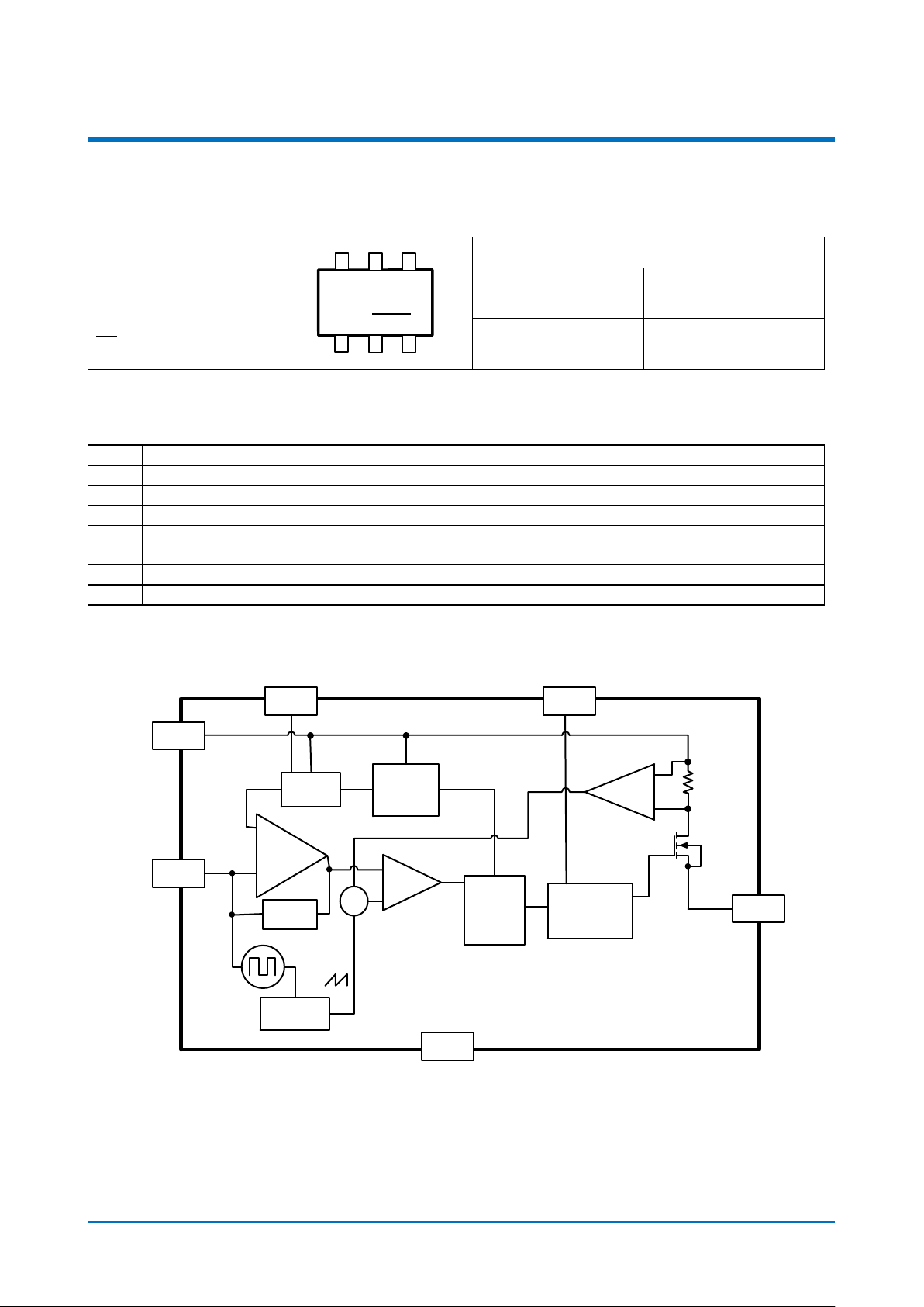
The BL8095 is a high efficiency current-mode
asynchronous, 24V/1.2A buck converter. Its input
voltage ranges from 4V to 24V and it provides an
adjustable regulated output voltage from 0.810V
to 5.5V while delivering up to 1.2A of output
current.
The switching frequency is set to 1.4MHz, which
works with a inductor as small as 4.7uH. And the
BL8095 will automatically switch between PFM
and PWM mode based on the load current, thus
to enhance the converter efficiency at light load.
BL8095 consists of many protection blocks such
as UVLO, input voltage over voltage protection to
stand much higher input voltage spike, thermal
protection and output short circuit protection.
The BL8095 is available in the tiny SOT23-6
package.
FEATURES
Adjustable Output Voltage, Vfb=0.810V
Output current is up to 1.2A
Range of operation input voltage: 4-24V
Input voltage UVLO: 3.7V (voltage decreasing)
Input Overvoltage Protection @26V
Withstand input voltage spike >30V
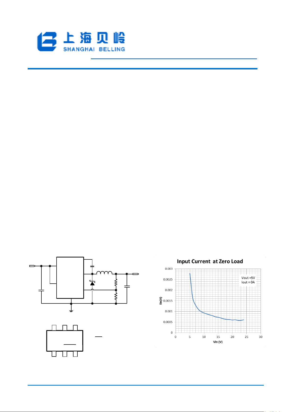
Operating current at zero load: 0.8mA (typ.)
Line regulation: 0.1%/V (typ.)
Load regulation: 10mV (typ.)
High efficiency, up to 90%
Environment Temperature: -20C~85C
APPLICATIONS
Security Camera
Consumer Electronic Device for automobile
Portable DVD
ADSL Modem, WLAN router
Other 12V or double cell Li-ion battery
powered device
TYPICAL APPLICATION and PIN OUT
LOW CURRENT CONSUMPTION
www.belling.com.cn 1

BL8095
Mark Explanation Ordering Information
HB: Product Code
YW: Date code
Product ID
BL8095CB6TR
Devices per reel
3000
PIN #
NAME
DESCRIPTION
1
BST
High side power transistor gate drive boost input
2
GND
Ground.
3
FB
Feedback input with reference voltage set to 0.810V
4
EN
Enable input. Setting it to high level or connecting to Vin via a resistor may turn on the chip,
while setting it to ground level will turn off the chip.
5
VIN
Power input, the input capacitor should be placed as close to VIN and GND pin as possible
6
SW
Power switching node to connect inductor
REG
&REF
PWM
Logic
DRIVER
FB
+
+
-
Slope Comp
OSC
Σ
VIN
BST
SW
GND
UVLO &
Thermal
shutdown
Current
Sense
EA
+
-
-
EN
COMP
network
SW
FB
EN
GND
VIN
HB
YW
BST
2 3
6
5 4
1
MARK and ORDERING INFORMATION
PINOUT DESCRIPTION
BLOCK DIAGRAM
www.belling.com.cn 2

BL8095
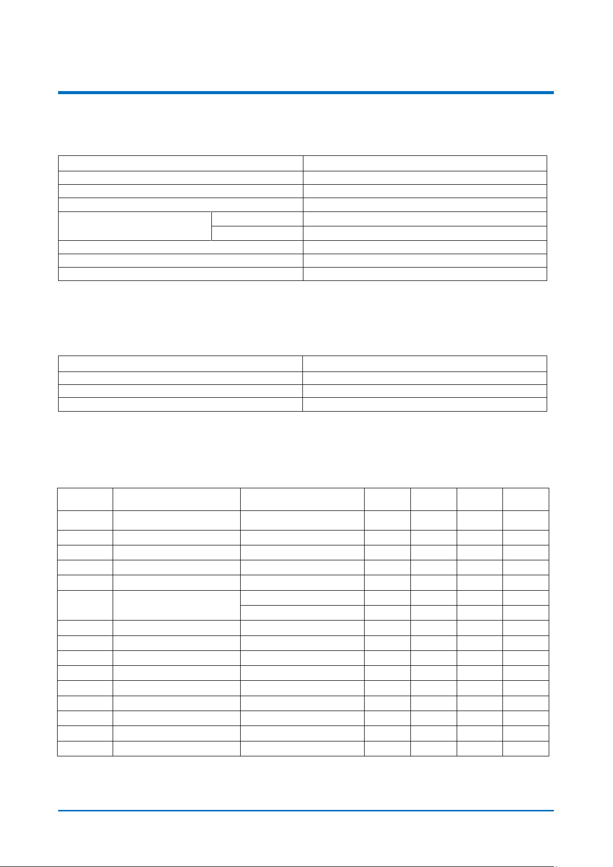
Parameter
Value
Max Input Voltage
30V
Max Operating Junction Temperature(Tj)
125C
Ambient Temperature(Ta)
-20C – 85C
Package Thermal Resistance
SOT23-6 (JC)
110C / W
SOT23-6 (JA)
220C / W
Storage Temperature(Ts)
-40C - 150C
Lead Temperature & Time
260C, 10S
ESD (HBM)
>2000V
Parameter
Value
Input Voltage Range
4V - 24V
Output Voltage Range
0.81 – 5.5V
Operating Junction Temperature(Tj)
-20C –125C
Symbol
Parameter
Conditions
Min
Typ
Max
Unit
VDD
Input Voltage Range
4
24
V
VOUT
Output Voltage Range
0.81 5.5 V Vref
Feedback Voltage
Vin=12V, Ven=5V
0.790
0.810
0.830
V
V
UVLO
UVLO Voltage
Vin H-->L, Iout=0.5A
3.7 V Ifb
Feedback Leakage current
0.1
0.4
uA
Iq
Quiescent Current
Active, Vfb=1V, No Switching
0.6
1.0
mA
Shutdown, Vin=8V
6
10
uA
LnReg
Line Regulation
Vin=5V to 12V
0.1
%/V
LdReg
Load Regulation
Iout=0.1 to 1.2A
0.02
%/A
Fsoc
Switching Frequency
Ven=3V, Vin=12V
1.0
1.4
1.8
MHz
RdsonH
High side Switch Rdson
Isw=200mA
250
350
mohm
Ilimit
Peak Inductor Current Limit
Vin=12V, Vout=5V
1.5 2 A
Venh
EN High Threshold
1
1.5 3 V
Venl
EN Low Threshold
0.5 V Vovp
Input Over-Voltage Protection
Ven=3V 26 V
TSD
Over Temperature Proection
Hystersis=40C
150
C
ABSOLUTE MAXIMUM RATING
Note: Exceed these limits to damage to the device. Exposure to absolute maximum rating conditions may affect
device reliability.
RECOMMENDED WORK CONDITIONS
ELECTRICAL CHARACTERISTICS
(VIN=12V, TA=25C)
www.belling.com.cn 3
 Loading...