

Page 1

AV110T Service Manual
Contents
chapter One Brief Introduction to Product
Section One General description
Section Two Functions and features
Chapter Two Operating Principle
Section One Overall structure
Section Two Volume board
Section Three Signal processing board
Section Four CPU board
Section Five Panel control and display circui
Section Six Power amplifier board
Section Seven Video board
Chapter Three Servicing Process
1. No output for Karaoke
2. Power supply not connected
3. No on screen display (OSD)
4. No output
Schematic & pcb wiring diagram
Spare parts list
Page 2

Chapter One Brief Introduction to Product
Section One General Description
AV110T is a 5.1CH audio power amplifier for home theatre usage. On the
basis of AV100, the follows are newly added functions:
1.1.1 Digital tuning function;
1.1.2 Video switch function;
1.1.3 Headphone output function;
1.1.4 Scene surround sound function.
Section Two Functions and features
1.2.1 Two-way audio signal input: VCD, DVD;
1.2.2 With 5.1CH input terminal, capable of connection with AC-3, DTS decode
output signal;
1.2.3 One way subwoofer signal line output, capable of connecting with active
subwoofer speaker;
1.2.4 Automatically signal search when power on;
1.2.5 6CH digital volume control and separate channel level adjustment;
1.2.6 Three sound field modes: Hi-Fi, Standard and Cyber Logic;
1.2.7 Six preset EQ modes, multi-band electronic equalization adjustment;
1.2.8 Save/Call of user-set parameter;
1.2.9 Digital Karaoke, with microphone volume, echo and delay adjustment;
1.2.10 Auto mute function;
1.2.11 Dynamic display screen; multiple spectrum display modes; English
intelligent operation interface;
1.2.12 Bass enhancer function;
1.2.13 Full remote control operation.
Page 3

Chapter Two Operating Principle
Section One Overall structure
The whole unit of AV110T is mainly composed of the following parts:
2.1.1 Volume board: input selection, Cyber Logic and bass enhancer control.
2.1.2 Signal processing board: Karaoke signal processing and front stage
amplifying of 5.1Ch signal.
2.1.3 CPU board: whole machine control unit, breadth sampling circuit and
auto searching circuit.
2.1.4 Control panel: LCD display, remote control and keyboard scanning and
fulfill man-machine conversation function.
2.1.5 Power amplifier board: supply operating voltage required for each unit
circuit, and perform power amplifying for 5.1Ch signal or analog signal.
2.1.6 Tuner: receive radio signal and then send to power amplifier to perform
signal processing.
2.1.7 Video input and output board: fulfill video input and video switch function.
Section Two Volume board
AV110T has 4 kinds of input modes in all: FM/AM, VCD, DVD and 5.1CH.
Page 4
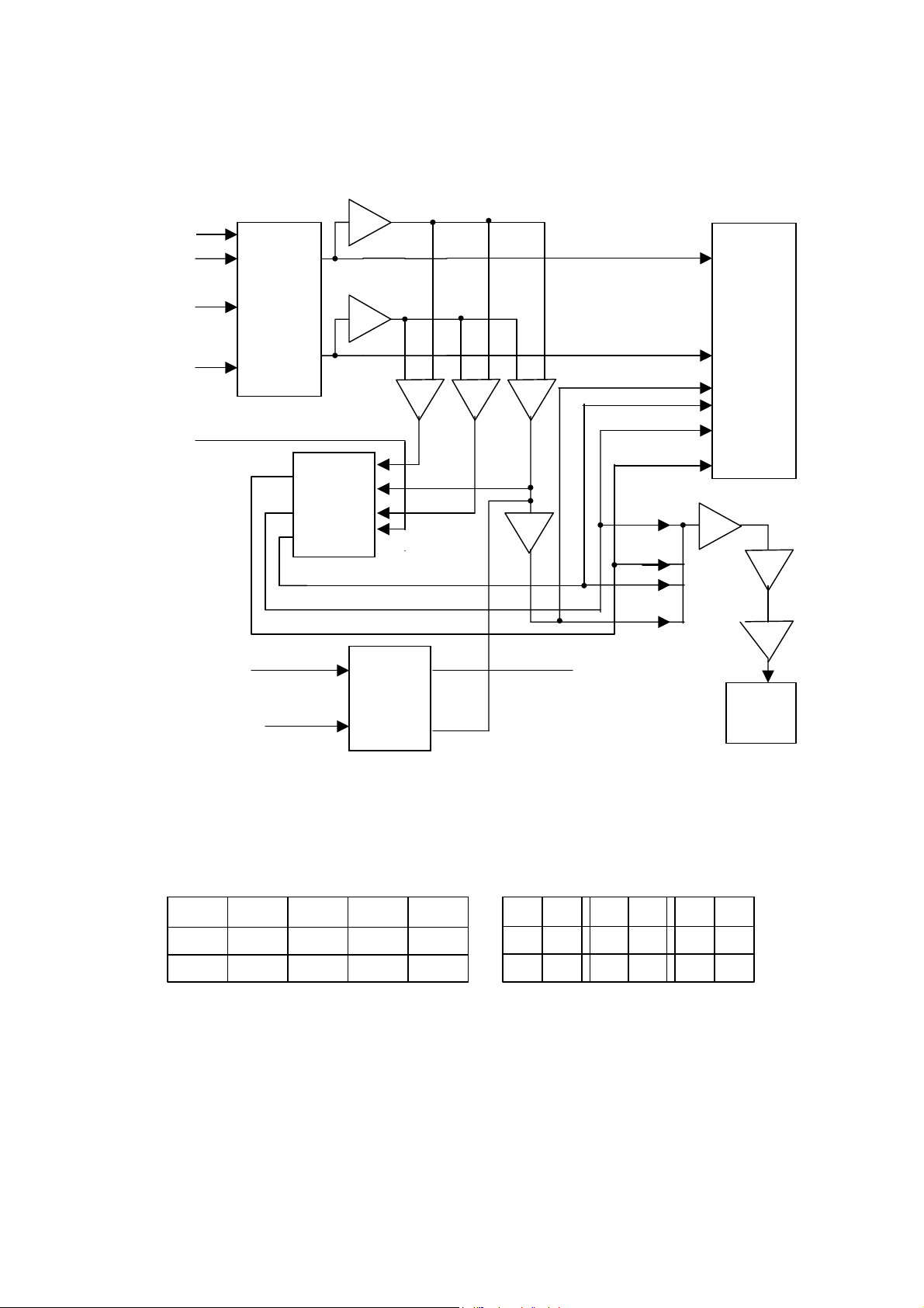
By sampling from L/R channel of AV110T, after Cyber Logic function, C, SL and
L
A
A
SW channel signals are achieved. In this circuit, electronic analog switch is
adopted to fulfill the switch in all states, and the signal flow chart is as follows:
FM/AM
VCD
5.l input
L, R
Channel
5.1 input
C, SR, S
channel
CD4052
Input
selection
SL
SR
c
CD4053
Electronic
switch
L
R
SW
C
SR
SL
15
13
6
11
8
9
N106
M62446
Electronic
volume
adjustment
N108B
N103A
N103B
5.1 input
SW CH
SW1
CD4053
Electronic
switch
SW
Send to L/R
SEARCH
N100
CPU
2.2.1 Input selection and sound field processing mode
The input selection of AV110T is achieved via electronic switches CD4052
and CD4053, and the truth tables are as follows:
CD4052 Truth table
5.1 VCD DVDTuner
B
0
0
0
1
1
0
1
1
CD4053 Truth table
XBY C
0
1
X0
X1 1
0
Y0
Y1
Z
0
Z0
Z1
1
5.1CH input mode: Now A/B/5.1CH control pins of M62446 are in high level.
L/R channel signals of 5.1 input terminal is outputted from pin 3/13 of N101
and sent to IC N106 for volume and tone adjustment; meanwhile, C/SR/SL
signals of 5.1CH input terminal are outputted from pin 14/15/4 of N102 and
then respectively sent to IC N106 for independent volume adjustment. And SW
signal of 5.1CH is outputted via pin 4 of N103 and then sent to M62446 after
being amplified by N107A.
Three analog input modes: AV110T totally has three analog input modes:
Page 5
digital tuning demodulation signal, VCD and DVD, which are controlled via A/B
g
T
t
signal respectively.
AV110T totally has three sound field modes: Standard, Cyber Logic and Hi-Fi.
1. Standard: Under the control of overall CPU, when bass enhancer is off, L/R
channel and subwoofer output are available; when bass enhancer is on,
only L/R channel output is available.
2. Hi-Fi: Under the control of overall CPU, only L/R channel output is available
to M62446.
3. Cyber Logic: Pin 9/10 of electronic switch N101 (CD4052) select a group of
analog L/R channel input signals according to the truth table. L/R signals
are outputted from pin 13/3 via the internal electronic switch of N101, and
divided into two ways. One way is respectively sent into pin 13/15 of
M62446 for electronic volume and tone adjustment. The other way
produces SW/S-SR/S-SL and S-C signals via buffer, adder-subtractor and
low-pass filter. S-C/S-SR/S-SL signals are sent to pin 12/2/5 of N102. N102
select Cyber Logic signal input (see CD4053 truth table) from Cyber Logic
and 5.1Ch signals, outputs C/SR/SL signals from pin 14/15/4 and sends
into pin 11/8/9 of M62446 for volume adjustment. Still another way of SW
signal directly sends to pin 6 of M62446 after being outputted from N107A.
5.1CH signal sent into M62446 is outputted from pin 31-36 after volume
and tone adjustment, and then outputted to signal board by XS20 power
distributor.
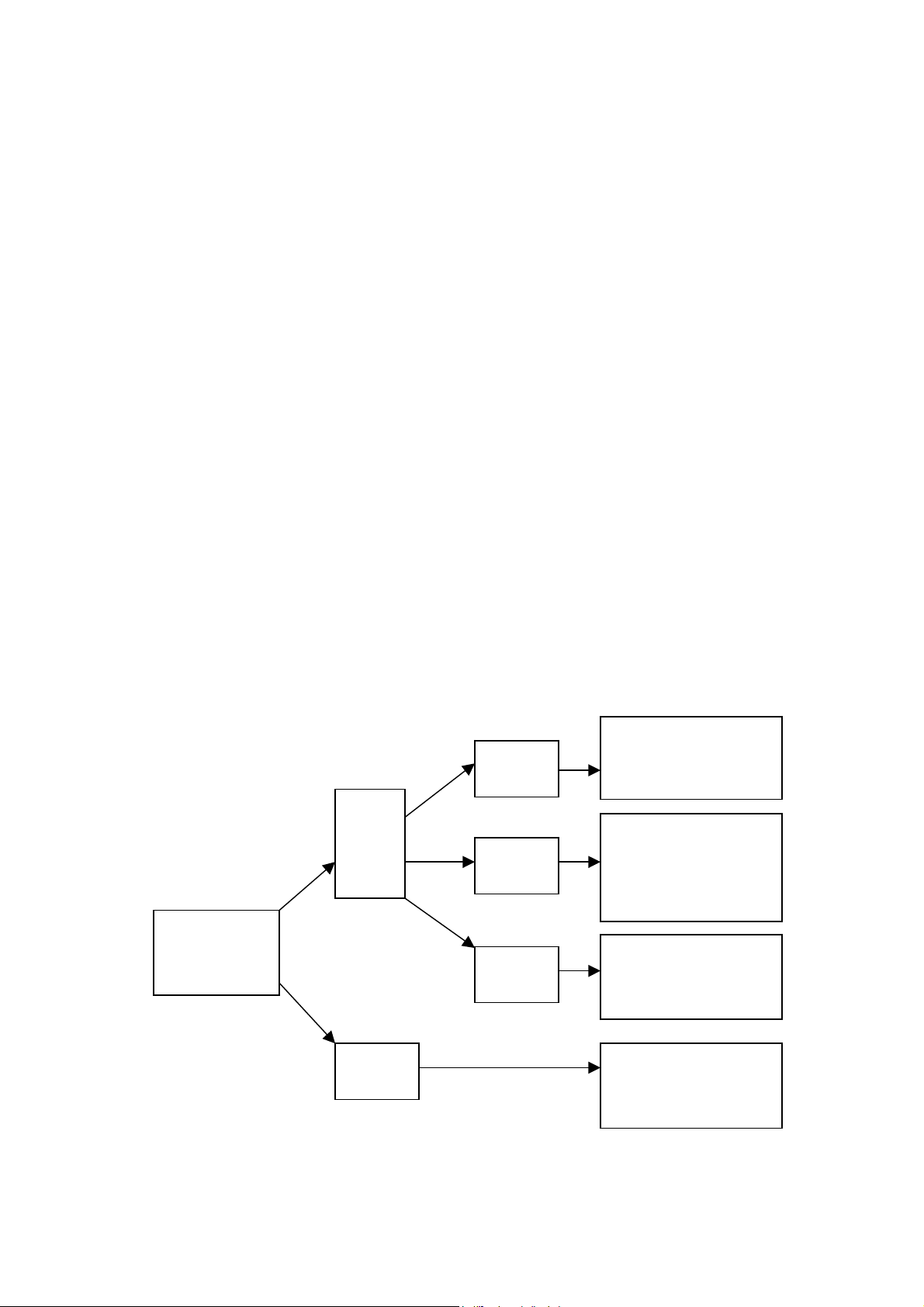
The relation between sound sources in input circuit and sound processing
modes is as the following figure.
Press INPU
button to selec
circularly
Two
analog
input
modes
Hi-Fi
Standard
Cyber
Lo
ic
Only L/R channel output.
Sound field and EQ setup
invalid
Only L/R/SW channel
output. Concert hall
sound field and EQ setup
available
6CH output. Theatre
sound field and EQ setup
available
5.1 input
mode
6CH output. Theatre
sound field and EQ
setup available
Page 6

2.2.2 Control circuit
Pin 23/26/27 of CPU (N100) output data, PVST and clock signals send to pin
39/40/41 of M62446, control pin 1/2/3/4 of M62446 output control level, so as
to select input signal and spectrum sampling signal. It is worth noting that
PVST signal is a latch control signal. When data and clock of CPU are sent to
M62446, an identification signal will be added, indicating that this signal can
2
only be used by M62446 while other IC of I
C bus cannot use current data and
clock signal.
2.2.3 Frequency spectrum sampling circuit
Only S-C/S-SR/S-SL/SW signals are sampled during frequency spectrum
sampling in AV110T and added to pin 14 of N103 via a 150K sampling resistor.
Another S-C cyber logic signal is added to pin 1 of N103, called S-C'. 5.1CH
and LR-T of M62446 select sampling signals. When cyber logic is selected, the
control signal of 5.1CH is of low level while pin 9/11 of N103 is of low level.
According to the truth table, it is known that the outputs are X0/Z0. Sampling
signal is grounded while LR-T is of H level. Select Y1, S-C'signal is outputted
from pin 15 of N103 to N108B, adding to OK-R signal for the amplification of
frequency spectrum signal, and then sent to frequency point gating and auto
search circuits via XS20.
2.2.4 Tuning function
The tuning function directly controls tuner and receives audio frequency signal
mainly via CPU and then outputs after amplification via power amplifier. The
clock and data line of tuner are shared with LM62446 and the other two control
lines are connected to CPU directly. L, R signal processed by the tuner can be
sent to N101 IC CD4052 directly to input the selected channel.
Section Three Signal processing board
The signal processing board superposes, mixes and amplifies 5.1CH signal
sent from the volume board, voice signal from the voice board and Karaoke
signal.
2.3.1 Karaoke circuit of AV110T
This circuit processes human voice through power amplifier and reproduces it
via speaker. It includes human voice beautification circuit, wide sound field
processing circuit, Karaoke echo and delay adjusting circuit.
IC and its functions for Karaoke:
S.N. of IC Name of IC Functions of IC
N201 PT2308 Transmittal, pre-amplification for Karaoke signal
N200 PT2315 Karaoke volume control, including tone control
N205 CD4053 Electronic switch
N209 PT2399 Karaoke echo processing
N207 CD4051 Karaoke delay adjustment
N208 CD4051 Karaoke echo adjustment
N204 4558 Phase inverter
Page 7
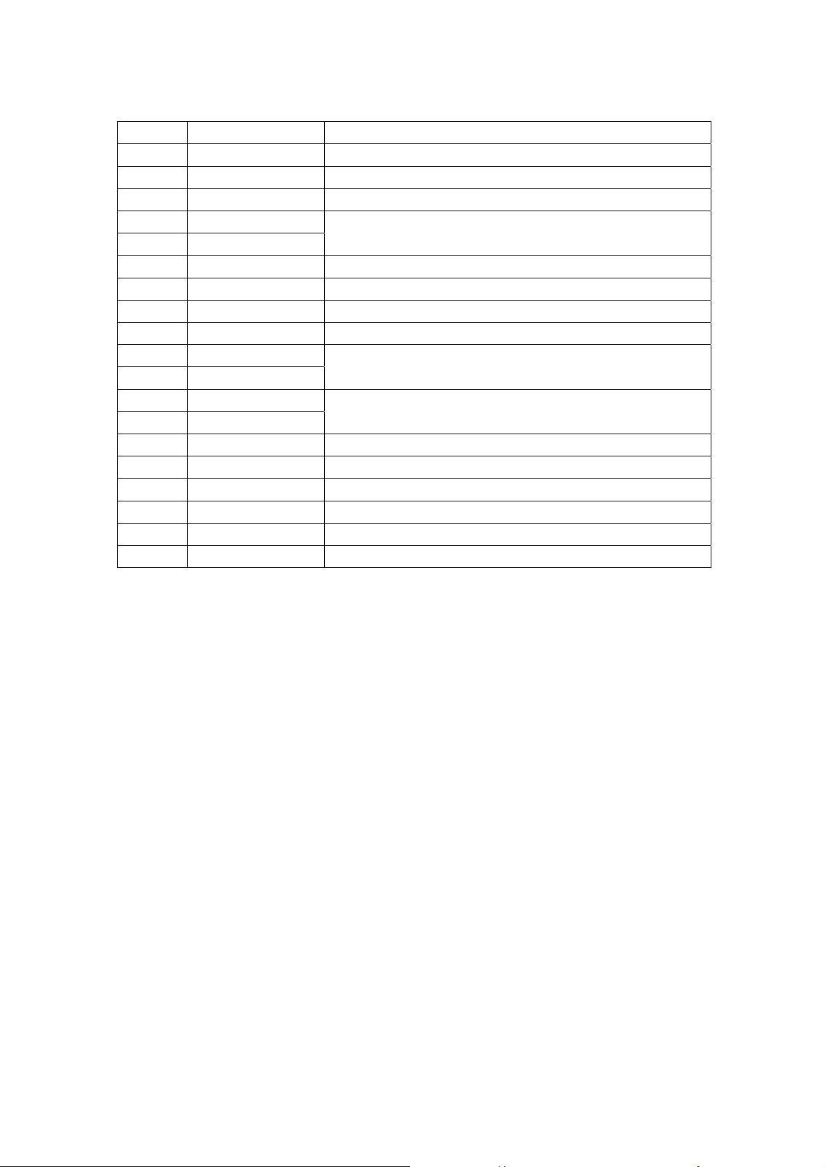
PT2315 functional pin
S.N. Name of pin Description
1 REF Reference voltage (1/2VDD)
2 VDD Power supply
3 AGND Analog
4 TREB L
5 TREB R
6 RIN R channel input
7 LOUD-R Loudness control pin of R channel
9 LOUD-L Loudness control pin of LR channel
11 LIN L channel input
12 BIN L
13 BOUT L
14 BIN R
15 BOUT R
16 RFOUT R channel output
17 LFOUT L channel output
18 DGND Digital
19 DATA Control data of sequence transmission (DATA)
20 LCK Clock input of sequence transmission
8,10 NC Not connected
2.3.2 Flow chart of Karaoke signal
When the microphone is inserted, MIC signal is sent via MIC to the transmittal
circuit combined by N201A for amplification. Amplified MIC signal gives CPU a
MIC identification signal after N202A amplification, followed by VD201
rectification and filtering control triode V200. CPU sends PKM signal, which is
of low level, causing cutoff of triode V103/V105 and enabling output of MIC
signals; another way reaches pin 6 and 11 of PT2315 after C219/C222
coupling, outputs from pin 16/17 after internal volume and tone control, mixed
into one way and sent to N202B and then reversely send to N203B for
amplification. Signals amplified by N203B are divided into two ways: one way
is directly outputted; and the other way is outputted from pin 14 after being
coupled by R222/C247 to PT2399 for internal delayed echo adjustment,
reversed by N204B and outputted by mixing with karaoke signal. While OK-R
is outputted from pin 14 after being gated by N205 and superposed to L/R
channel.
In this circuit, the bass boost network made up of triode V201 connected to the
negative terminal of N202B is primarily for bass boost of 75HZ low frequency
signal.
During delay adjustment for PT2399, first control signal is given to CPU, which
controls N207 after being expanded via N211 IC CD4094 and connects with
pin 6 of PT2399 by selecting different resistance values for purpose of delay
adjustment.
Treble control pin of L/R channel
Bass control input/output pin of L channel
Bass control input/output pin of R channel
Page 8

Echo control is to change the resistance value at the connection point to R229,
so as to change the superposition on through connect signal for echo control.
The wide sound field processing control signal of SOK’s karaoke is in wide
sound field mode when it is high level, and now the signal of OK-R is the OK
signal inverted by N204A.
A sense signal of OK-SW on the MIC plug detection together with the network
made up of V200. When MIC is not plugged, it is low level; when plugged, it is
of high level.
Karaoke auto mute function is also available. When P-KT fails to detect signal
for a continuous period, CPU will send a P-KM signal to mute karaoke and
avoid MIC receiving noise, which may affect on sound effect.
Signal flow chart of scene mode
AV110T has a special function that switching between 5 scene modes is
available without karaoke, which is fulfilled through part of karaoke.
When pin 9/10 of N205 are of high level, sampled L/R/C signals are outputted
via pin 3 through N205 gating. After amplification by N203, one way is
connected directly; and another way is sent to internal of PT2399 for echo
delay adjustment (controlled by IC CD4049), with the adjusted effect
superposed to L/R/C channel to form different scene modes.
In this circuit, MIC shall not be inserted and is only available in 5.1CH mode.
N203A is for the purpose of reversal.
In addition, this device is added headphone output function. PHSW is low level
and each channel has output when headphone is not inserted. But when
headphone is inserted, PHSW will be high level for the mechanical settings
thus LRM and SCM signals change into high level at the same time to realize
muting in each channel, so the signal is only outputted from headphone, that is,
there is not signal output with each channel when connecting with headphone
output.
2.3.3 Bass enhancer circuit
P-BURST is the switch signal of bass enhancer. When it is of high level and
added to the base electrode of V102, V102 will be switched into conduction.
When the collector electrode outputs low level, V107 will be cutoff; when the
collector electrode is of low level, V100 will also be cutoff. SW signal is
normally outputted to external terminal. Meanwhile, the high level signal of
P-BURST is added to the emitter electrode of V108. V108 is positively biased
and switched into conduction. The collector electrode adds high level to the
base electrode of V101. V101 is positively biased and switched into conduction,
and ground SW signal, not superposing it to L/R signal.
In reverse, when P-BURST is of high level, V100 will be switched into
conduction and SWM cannot be outputted from external terminal. Meanwhile,
V101 is cut off and SW signal is superposed to L/R channel signal.
The bass enhancer of AV110T can be divided into three steps. This principle is
to change the volume of bass enhancer by changing the SW output volume of
M62446.
Page 9

2.3.4 Mixing and amplification circuit of 5.1 signal and karaoke signal
When L/R channel signal of 5.1 signal is superposed with SW signal and
amplified by N101B/N100B, it is sent to the reverse phase of N101A/N100A.
Meanwhile, OK-R/OK-L signals are also respectively added to the reverse
phases of N101A/N100A. After mixing and amplification by N100A/N101A,
they are respectively outputted from pin 1 of N100A/N101A to power
amplification circuit for power amplification.
Meanwhile, the C-1 signal sent by volume board is added to the reverse phase
of pin 6 of N102B and added to the reverse phase of N102A after amplification.
Now C1-1 signal after electronic echo processing is also added to the reverse
phase of N102A and sent to power amplification circuit after mixing and
amplification.
SR-1/SL-1 of another volume board is also added to the reverse phase of
N103B and N104B for amplification and then sent to N103A and N104A for
further amplification, and later sent to power amplification circuit.
One way of 5.1 signal after being mixed and amplified is sent to power
amplification circuit passing through XS9, and the other way forms DIST
(distortion error detecting signal) signal passing through
R111-R113/R142/R145/VD100-VD104, which will be added to CPU for
automatic gain adjustment, so as to control volume output.
Section Four CPU board
2.4.1 CPU control unit
N100, the overall CPU, is the overall control center, inputting all kinds of
control instructions to controlled circuits to achieve all kinds of control functions.
It adopts +5V supply with pin 40 as its supply pin. Pin 18 and pin 19 connect
externally with 12M crystal oscillator to provide working clock frequency for
itself. Pin 9 is its reset pin. When starting, +5V charges C106 via R100. The
voltage of two ends of capacitance cannot be mutated, thus B-pole of triode
V100 is low level, that is, V100 conduction gives a high-level reset signal to
CPU. When capacitance C106 finishes charge, V100 stops and then reset
finishes. The form of this reset circuit is to reset high level and keep low level.
When the machine is working, the static information of Power-on logo on
screen and Chinese characters are stored in CPU internal static memory.
N101, a status memory, can record the current working status of machine
when powering off and show the status when next time power on, avoiding
users to re-adjust. The sound field mode set by users is also stored in it and
can be called when necessary.
2.4.2 Detect input signal and automatically search circuit
DISPLAY signal from volume board is sent to N103A to amplify and limit level,
and then sent to inverse end of voltage comparator N103B after capacitance
coupling. It inputs from pin 7 of N103B and then is sent to pin 16 of CPU via
VD103, V101, R109 and R107. When N103B inputs a high level, VD103 is in
Page 10
reverse cut-off status, B-pole of switch tube V101 is high level and is in
A
3
A
conducting status, then gets an about +5V high level (signal input) to CPU after
VD101’s stabilization and stop searching. When the output end of N103B
outputs a low level, VD103 is in conducting status, B-pole of switching tube
V101 is low level and is in cut-off status, and then CPU detects the low level
(no signal input). Its working principles are as follows:
① After starting up, under CPU internal program’s control, a data signal is
outputted via pin 23 to M62446, and then M62446 scans each input port of
N101, N102 and N103 by emitting high and low levels. When the input ports
have no signal input, it automatically becomes standby status. When any of
ports has signal input, channel paths of input N101, N102 and N103 has A/C
signal which is amplified and limited level by N108B and N103A of CPU board,
then compares with pin 5 of N103B and gets plus-minus level close to supply
power. The co-phase voltage of N103B is about 0.1V. After the direct current
voltage is over 0.1V, the output end of N103B outputs low level is close to
negative-power voltage, VD103 positive-bias conducts, switch tube V101
(S9014) stops, emitter outputs a low level to pin 16 of CPU which by controlling
IC M62446 makes search level lock on the port through which signal inputs, to
enter normal play.
② When pressing “SEARCH” button on the remote controller, it is
converted from optical signal to electric signal by the remote control receiver of
panel. Pin 14 of CPU emits a high level to conduct V102 and search according
to the same previous process.
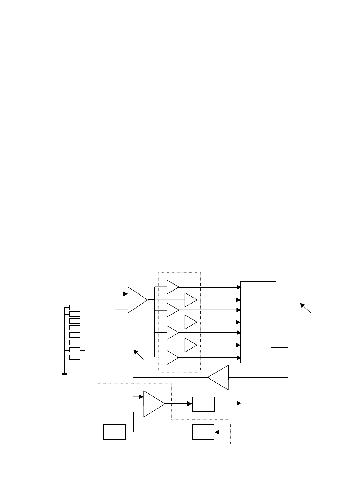
2.4.3 Spectrum Analysis Circuit (see the following figure)
Spectrum analysis circuit is divided into three parts:
DISPLAY
N104
CD4051
uto
spectru
m and
gain
adjustme
N105C
+
}
CPU
.
7-segment
band-pass
35HZ
134HZ
300HZ
1KHZ
2.2KHZ
6.3KHZ
16KHZ
N108
CD4051
Frequency
point
gating
}
3
-
+
N102A
V105
Pin 12 of CPU
+5V
.
V104V103
Pin 28 of CPU
/D conversion
CPU
Page 11

Automatic spectrum gain adjustment circuit: To avoid two situations that
A
spectrum display amplitude is too low when input signal is too weak or
spectrum display is in full screen when input signal is too strong, AV110T sets
automatic spectrum gain adjustment circuit, using a single-track
one-from-eight electronic analog switch, its true value diagram is as follows:
CD4051Truth table
X0 X1 X2 X3
1
B
C
0
0
0
0
0
1
Its main working principle is to change the value of inverse ground resistanc
X4 X5 X6 X7
1
0
1
0
1
00 0
1
01
1
1
0
1
1
1
e
of transmittal N104 to change the transmittal gain multiple. Let’s see the
detailed work of the whole circuit. We’ve referred that spectrum analysis signal
source (DISPLAY) is sent to the co-phase input end of transmittal N105C to
amplify. Its amplification factor is determined by the value of the resistance
connecting with the electronic switch of its inverse end N104. When the main
volume is large, CPU will automatically increase the value of ground resistance
and decrease the amplification factor; when the main volume is small, CPU will
automatically decrease the value of ground resistance and increase the
amplification factor.
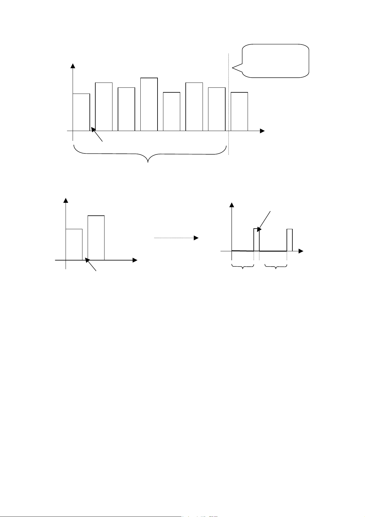
Amplitude samplin
g circuit: signal amplified by N105C is sent via C115
coupling to seven band-pass filters composed of transmittals. By setting its
capacity of feedback capacitance, its frequency-band range can be determined.
The frequency value of superscript of the output points is the central
frequency-point of the frequency band. The output end of each band-pass filter
is connected with a half-wave rectifier circuit. The amplified A/C signal is
rectified to direct current. The circuit is mainly to achieve frequency-point
sample. It can display the amplitude of all frequency-points of the whole sound
signal via direct-current voltage. If the low frequency of sound signal is
stronger, the current voltage of output end of 35HZ and 100HZ band-pass filter
is higher. When high frequency is stronger, the current voltage of 10K and 16K
band-pass filter is higher. The output ends of the seven band-pass filter are
connected with the seven input ends of electronic switch N108 (CD4051).
These electronic switches will quickly circularly-switch among frequency points
(referring to previous true value diagram). Pin 3 output end of N108 will output
a string voltage value representing frequency point signal amplitude (see next
diagram).
Page 12
V
35HZ
100HZ
300HZ
1KHZ
3KHZ
10KHZ
16KHZ
Note: the voltage
amplitude in diagram
is uncertain.
35HZ
Interval of switch
T
Frequency point cycle gating period
V
35H
100HZ
V
Discharge of high level
Interval of switch Ti Time for charge me for charge
T
35H
100HZ
T
/D conversion and output circuit display (two situations):
A
1. When no signal input, pin 28 of CPU sends a high level to B
-pole of V104.
The positive end of N102B is low voltage, the inverse end of N102B gets
partial voltage of R189 and R172, making N102B output a low level, that is,
triode V105 stops and C-pole of V105 will give a high level to pin 12 of CPU to
let CPU not conduct AD conversion (pin 6/7/8 of CPU are inactive and keep
high level).
2. When th
e machine has detected the signal (the inverse end of N102B has
a current voltage representing 35HZ signal amplitude), pin 28 of CPU is
converted into low level and +5V voltage charges for C137 via V103. When
reaching the voltage value of inverse end, the comparator converts and N102B
outputs high level. Once CPU receives low-level signal, it stops 35HZ level
gating and converts into next frequency point 100HZ. During conversion, pin
28 of CPU outputs an instant high level to conduct V104, leak the voltage
capacity of C137 and make the co-phase end of N102B restart to charge
100HZ from 0-level. When the charge of 100HZ finishes, the charge and
discharge of next frequency point begin, and such process occurs circularly
under the control of CPU. The charge time form 0-level to the occurrence of
Page 13

output conversion represents the signal amplitude of current frequency
point—the larger the amplitude, the longer the time and the amplitude
displaying in screen is higher; the smaller the amplitude, the shorter the time
and the amplitude displaying in screen is lower. Digital pulse outputted from
N102B output end is added by V105’s inverse to pin 12 of CPU which handle it
and output to panel to display dynamic frequency in screen. The display of
original frequency points is sequential. However, the above circular process is
extremely quick, thus, what we see in screen is the progress of the whole
spectrum displaying synchronously.
Section Five Panel control and display circuit
The panel control and display circuit of AV110 adopts the special IC 101
(PT6311), whose external buttons of pin 10/11/12/13 scan buttons matrix. After
receiving the control command of users to the machine, processing is done
inside and then outputted by two ways: one way is sent to display screen to
display the working status; and the other way is transmitted to CPU through pin
5/6/8/9 to ask for performing and finishing the corresponding control function.
N102 is remote control receiver, which transforms the received infrared remote
control signal into electronic signal and then send it to pin 13 of CPU so as to
complete remote control function.
Section Six Power amplifier board
2.5.1 Power supply
This part is used to p
circuit. The circuit diagram of power supply is shown as follows:
rovide all kinds of required working voltage for all unit
Page 14

Through the flat cable XP8, the first group output of transformer provides
filament voltage for display screen, and provides working power supply for
display drive ICPT6311.
The second group output of transformer is outputted by flat cable XP3 to the
power supply part of power amplifier board. After being rectified by rectification
diode 5404, two groups of anode and cathode power supply are achieved,
which respectively provide two groups of anode and cathode working power
supply for the main channel power amplification circuit of power amplifier
board and center/surround channel power amplification circuit.
The third group output of transformer is outputted by the flat cable XP23 to the
signal processing board. After being rectified by rectification diode, voltage
regulated by the voltage regulator 7805 and +5V power supply is outputted.
2.5.2 Power amplification
Main channel and center surround audio signals are processed by signal
processing board, and then inputted by flat cable XP200 to power amplification
circuit to perform amplification respectively. L and R channels are respectively
amplified by the special audio usage integrated power IC N200 and N201
TDA7296. LS and RS channels are amplified by a dual-transmittal integrated
power IC N202 TDA7265. Center channel is amplified by the integrated power
IC N203 TDA7298.
The used IC TDA7296 has the following features (attached with materials of
TDA7296):
1. High voltage range:±35V;
2. Power: 60W (4 ohm);
3. With mute and standby function;
Page 15

4. Complete protection circuit: over-current and over-heat protection;
5. Packaging: dual line pin 15.
The used IC TDA7265 has the following features (attached with materials of
TDA726):
1. Complete protection circuit: grounding short-circuit and over-heat
protection;
2. Power supply voltage range:±5~±25V;
3. Packaging: dual line pin 11;
4. Power: 2*25W (4 ohm);
5. With mute function.
The used IC TDA7298 has the following features (attached with materials of
TDA7298):
1. Complete protection circuit: short-circuit and over-0heat protection;
2. Power supply voltage range:±22V;
3. Packaging: dual line pin 7;
4. Power: 28W (4 ohm);
5. With mute/standby function.
2.5.3 Anti impulsive sound circuit when power-on
When powering on, this circuit makes TDA7296 to complete “standby --- mute
--- work” process and has effectively removed the impulsive sound when
power-on. When powering off, this circuit makes TDA7296 to complete “work
--- mute --- standby” process and has effectively removed the impulsive sound
when power-off.
Page 16

Section Seven Video board
Video board fulfills the functions of input, output and switch of the video, with
the schematic diagram shown as the following figure:
This switch function is realized through an electronic switch IC CD4051. When
high and low level of control signal A and B are changing, IC CD4051 switches
between VCD and DVD, and video signal is outputted by pin 3 VOUT.
Page 17

Chapter Three Servicing Process
r
f
y
f
f
1. No output for Karaoke
Firstly confirm whethe
microphone is good.
Whether the pre-amplification
circuit and checking circuit o
microphone work normally.
Whether the microphone
volume adjustment works
normally.
Whether high/low frequenc
boost circuit works normally.
Whether mute circuit o
microphone works normally.
Yes
Yes
Yes
Yes
Note: For MIC size is disordered on the market,
that MIC is too long or too short will both lead to
no output of microphone.
Note: here please check whether the
microphone checking signal P-KT is able to
overturn when signal output is available.
Note: check whether the periphery circuit o
volume boost IC2315 or IC M62429 is normal,
and whether the voltage and data line has
abnormalities.
Note: check whether the triode in the
microphone mute circuit has damage, and
whether the mute control signal line P-KM is
normal.
Page 18

2. Power supply not connected
y
r
y
Check whether the power cord
socket has been well connected.
Yes
Whether fuse FL100 is
2. The primary internal circuit
complete and good.
Yes
Check the primary coil
resistance numerical
value of transformer.
Yes
No
No
Check whether the secondar
voltage of transformer is normal.
In most cases, primary short-circuit
of transformer will burn out this fuse.
1. If primary internal short
circuit of transformer occurs,
the resistance numerical value
will decrease, fuse will be burnt
and power supply will not be
connected.
opening of transformer leads
to disconnection of power
supply.
No
The short-circuit and circuit
opening inside the transforme
secondary coil lead to abnormal
output of secondary voltage.
Whether the input and
output of three-terminal
voltage regulator are
abnormal.
Whether power suppl
voltage of pin 40 of CPU
is normal.
Whether the
secondary fuse is
complete and good.
Whether the output
voltage of rectifier tube
is normal.
Whether the control panel
IC and display screen
voltage is normal.
Page 19

3. No on screen display (OSD)
f
f
f
r
r
g
No
Note: The abnormality o
the secondary output
voltage of transforme
may probably cause no
OSD.
Check whether the
filament voltage o
display screen is normal.
No
Whether the power o
control panel IC is
normal.
No
Yes
Yes
Check whether the data line
between CPU and control
panel drive IC and clock line
signals are normal.
Yes
Note: If display screen has
air leakage, it will cause no
OSD and now the filament
voltage is close to be low.
No
Whether CPU powe
supply is normal.
Yes
No
Whether signals from control
panel drive IC to display screen
pin are normal.
Can judge that the
Ye s
problem occurs in CPU
board.
Yes
May probably cause
the badness of control
panel drive IC.
Can judge that
display screen is
not
ood.
Page 20

4. No output
r
r
r
r
Check whether the analog
electronic switch IC can be
gated in this path when there
is signal input.
No
Note: check whether IC powe
cord is normal, and signal
cords P-INA and P-INB which
control IC gating are normal.
Check whether tone adjustment
IC62446 or 75347 front stage
has signal input.
Yes
Check whether power-on
checking circuit works normally.
Yes
Yes
Check whether tone adjustment
IC62446 or 75347 front stage
has signal input.
No
Yes
Check periphery circuit of IC is
normal; IC power supply; and
whether CPU control signals
P-VDA, P-VCK and P-VST are
normal.
Whether powe
amplifier board
has signal input.
Whether power amplifie
board has signal input.
Check whether powe
tube has abnormalities
of punch hole.
Whether main channel mute control
line P-LRM and center surround
mute control line P-CSM are normal.
Page 21

Schematic & pcb wiring diagram
Input board
Page 22

Signal processing board
Page 23

Page 24

Power amplifier board
Page 25

Page 26

Panel control board
CPU control board
Page 27

Microphone board
Page 28

Video board
Page 29

Spare parts list
Page 30

Signal processing board
Page 31

Page 32

Power amplifier board
Page 33

Page 34

Input board
Page 35

Panel control board
Page 36

Microphone board
Page 37

Video board
CPU control board
Page 38

Page 39

 Loading...