

Page 1

CONTENTS
1. SAFETY PRECAUTIONS……………………………………………………….. 1
1.1 GENENRAL GUIDELINES……………………………………………………….. 1
2. PREVENTION OF ELECTRO STATIC DISCHARGE(ESD) TO ELECTROSTATICALLY
SENSITIVE(ES) DEVICES………………………………………………………. 1
3. PRECAUTION OF LASTER DIODE……………………………………………. 2
4. GENERAL DESCRIPTION……………………………………………………… 3
5. PREVENTION OF STATIC ELECTRICITY DISCHARGE…………………….. 5
5.1 GROUNDING FOR ELECTROSTATIC BREAKDOWN PREVENTION……… 5
5.1.1 WORKTABLE GROUNDING…………………………………………………… 5
5.1.2 HUMAN BODY GROUNDING…………………………………………………. 5
5.1.3 HANDING OF OPTICAL PICKUP……………………………………………… 5
5.2 HANDING PRECAUTIONS FOR TRAVERSE UNIT(OPTICAL PICKUP).. 5
6. ASSENBLING AND DISASSEMBLING THE MECHANISM UNIT…….. 6
6.1 DISASSEMBLY PROCEDURE………………………………………………… 6
6.2 TERMINAL P.C.B………………………………………………………………. 6
6.3 CLAMP PLATE UNIT………………………………………………………….. 7
6.4 TRAY…………………………………………………………………………… 7
6.5 TRAVERSE BLOCK…………………………………………………………… 8
6.6 TRAVERSE GEAR……………………………………………………………… 8
6.7 OPTICAL PICKUP UNIT……………………………………………………… 9
6.7.1 PRECAUTIONS IN OPTICAL PICKUP REPLACEMENT…………………… 9
6.8 DISASSEMBLING THE MIDDLE CHASSIS…………………………………. 11
6.9 DISASSENBLING THE TRAVERSE GRAR A………………………………... 11
6.10 DISASSEMBLING THE SPINDLE MOTOR UNIT…………………………… 11
7 Electrical Confirmation………………………………………………………….. 12
7.1 VIDEO OUTPUT(LUMINANCE SIGNAL) CONFIRMATION………………… 12
7.2 VIDEO OUTPUT(CHROMINANCE SIGNAL) CONFIRMATION……………. 13
8. MPEG CHECK WAVEFORM 14
9 IC BLOCK DIAGRAM & DESCRIPTION………………………………….. 16
10 BLOCK DIAGRAM…………………………………………………………… 35
11 SCHEMATIC & PCB WIRING DIATRAM....................................................................36
12 EXPODED VIEWS…………………………………………………………….
13. SPARE PARTS LIST..................................................................................
13. SPARE PARTS LIST..................................................................................
48
51
55
Page 2

1.SAFETY PRICAUTIONS
1.1 GENERAL GUIDELINES
1.When servicing,observe the original lead dress.ifa short circuit is found,replace all parts which have
been overheated or damaged by the short circuit.
2.After servicing,see to it that all the protective devices such as insulation bamiers,insulation papers
shields are properly installed.
3.After servicing,make the following leakage current checks to prevent the customer from being exposed
to thock hazards.
2.PREVENTION OF ELECTRO STATIC DISCHARGE(ESD) TO ELECTROSTATECALLY
SENSITIVE(ES) DEVICES
Some semiconductor(solid state)devices can be damaged easily by static electricity.Such components
commonly are called Electrostatically Sensitive(ES)Devices.Examples of typical ES devices are integrated
circuits and some field-effect transistorsand semiconductor chip components.The following techniques
should be used to help reduce the incidence of component damage caused by electro static discharge(ESD).
1.Immediately before handling any semiconductor component or semiconductor-equipped assembly,drain
off any ESDon your body by touching a known earth ground.Alteatively,obtain and wear a commercially
availabel discharging ESD wrist strap,which should be removed for potential shock reasons prior to
applying power to the unit under test.
2.After removing an electrical assembly equipped with ES devices,place the assembly on a conductive
surface such as alminum foil,to prevent electrostatic charge buildup or exposure of the assembly.
3.Use only a grounded-tip soldering iron to solder or unsolder ES devices.
4.Use only an anti-static solder removal device.Some solder removal devices not classified as anti-static
(ESD protected)can generate electrical charge sufficient to damage ES devices.
5.Do not use freon-propelled chemicals.These can generate electrical charges sufficient to damage ES
devices.
6.Do not remove a replacement ES device from its protective package until immediately before you are
ready to install if.(Most replacement ES devices are packaged with leads electrically shorted together by
conductive foam,alminum foil or comparable conductive material).
7.Immediately before removing the protective material from the leads of a aeplacement ES device,touch
the protective material to the chassis or circuit assembly into which the device will be installed.
Caution
Be sure no power is applied to the chassis or circuit,and observe all other safety precautions.
8.Minimize bodily motions when handling unpackaged replacement ES devices.(Otherwise hamless motion
such as the brushing together of your clothes fabric or the lifting of your foot from a carpeted floor can
generate static electricity(ESD)
1
Page 3
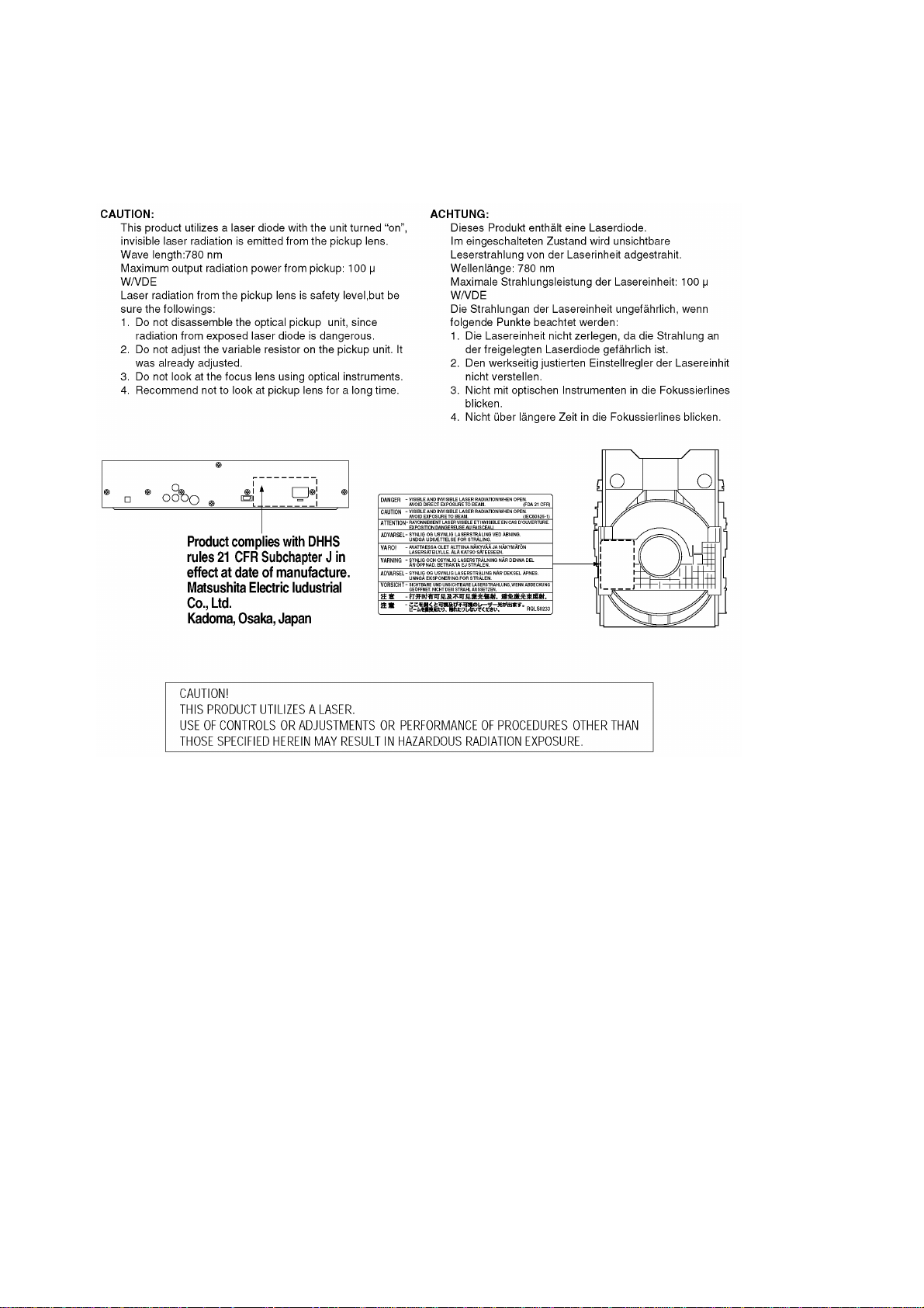
3. Precaution of L aster Diode
2
Page 4
DVD-AB908S
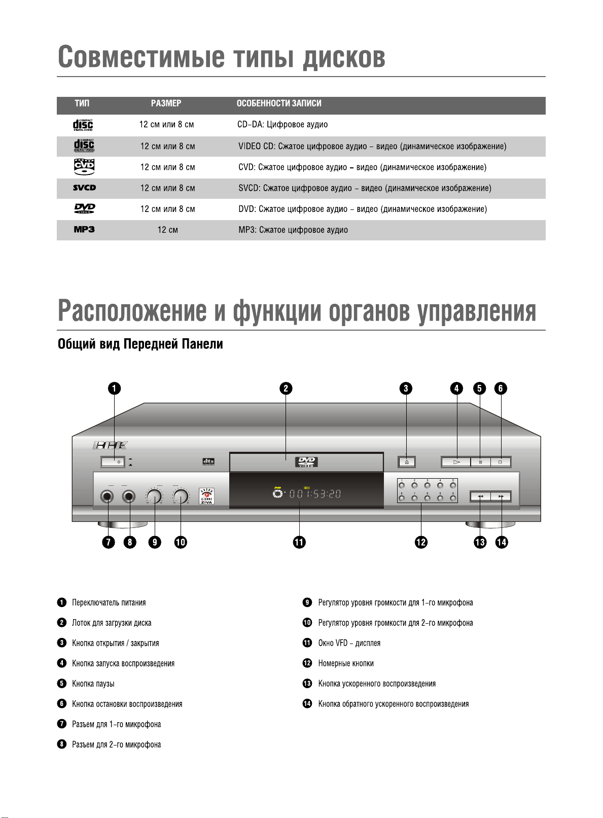
4.GENERAL DESCRIPTION
4.1
ON
POWER
OFF
MIC
1 12 2
VOL
PAUSE
OPEN CLOSE
PLAY
STOP
1
DVD / Super VCD / VCD / CD / MP3 PLAYER
REV FWD
3
Page 5
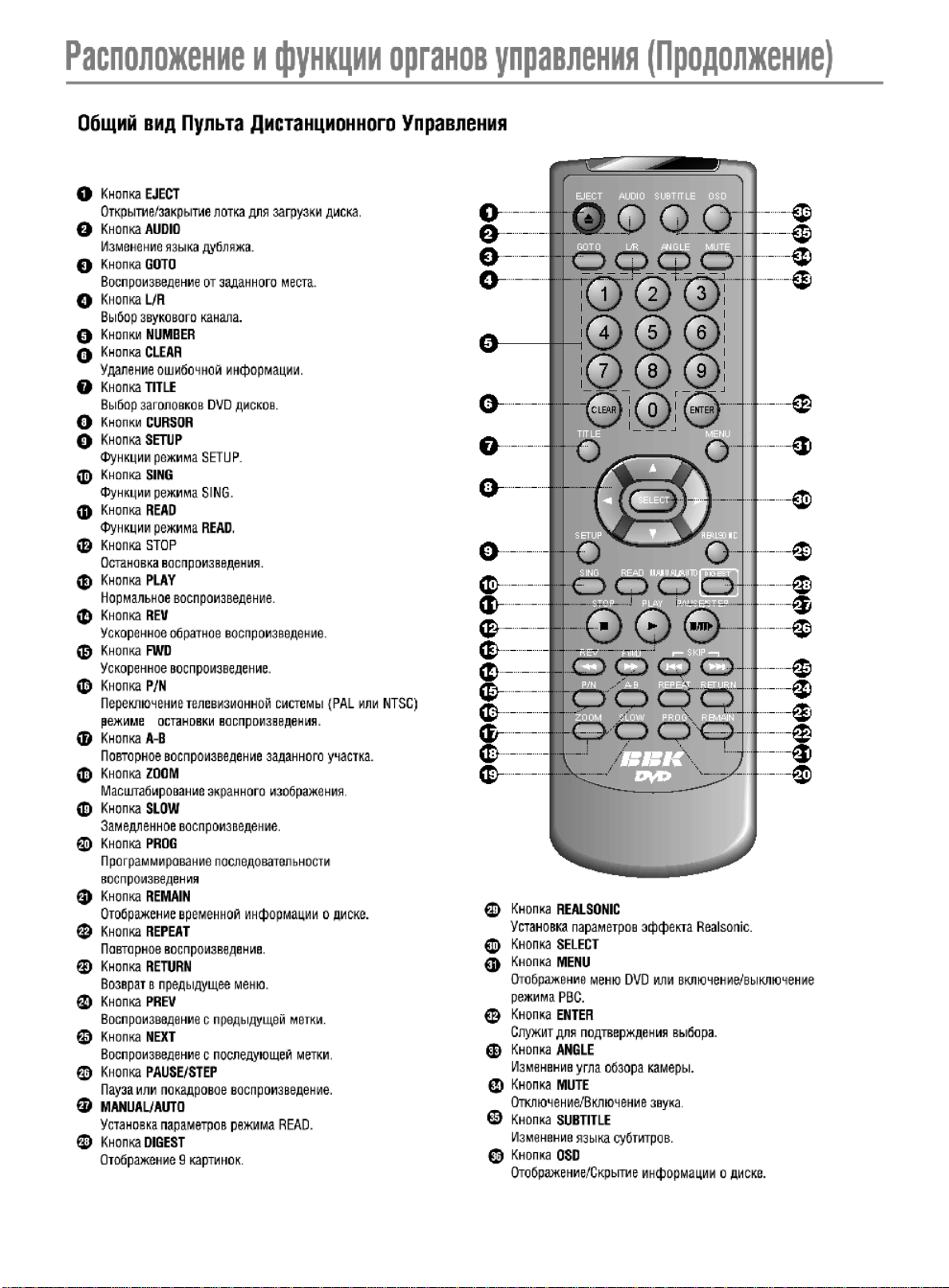
AUDIO
4.2
4
SUBTITLE
OSD
EJECT
36
2
3
L/R
ANGLE MUTEGOTO
4
1 2
3
35
34
33
5
4
7
6
CLEAR ENTER
TITLE
5
8
0
7
8
SETUP
SELECT
9
10
SING READ
11
STOP PLAY
12
13
14
15
16
REV
FWD
P/N RETURN
A-B
ZOOM REMAIN
SLOW
17
18
19
MANUAL AUTO
REPEAT
PROG
6
9
PAUSE STEP
SKIP
32
MENU
31
30
REALSONIC
29
DIGEST
28
27
26
25
24
23
22
21
20
Page 6
5.PREVERTION OF STATIC ELECTRICITY DISCHARGE
The laser diode in the traverse unit (optical pickup)may brake down due to static electricity of clothes or human body.
Some devices such as the DVD player use the optical pickup(laser diode)and the optical pickup will be damaged by
static electricity in the working environment.Proceed servicing works under the working environment where grounding
1.Put a conductive material(sheet)or iron sheet on the area where the optical pickup is placed,and ground the sheeet.
3.The flexible cable may be cut off if an excessive force is applied to it.Use caution when handling the cable.
Use due caution to electrostatic breakdown when servicing and handling the laser diode.
5.1.Grounding for electrostatic breakdown prevention
works is completed.
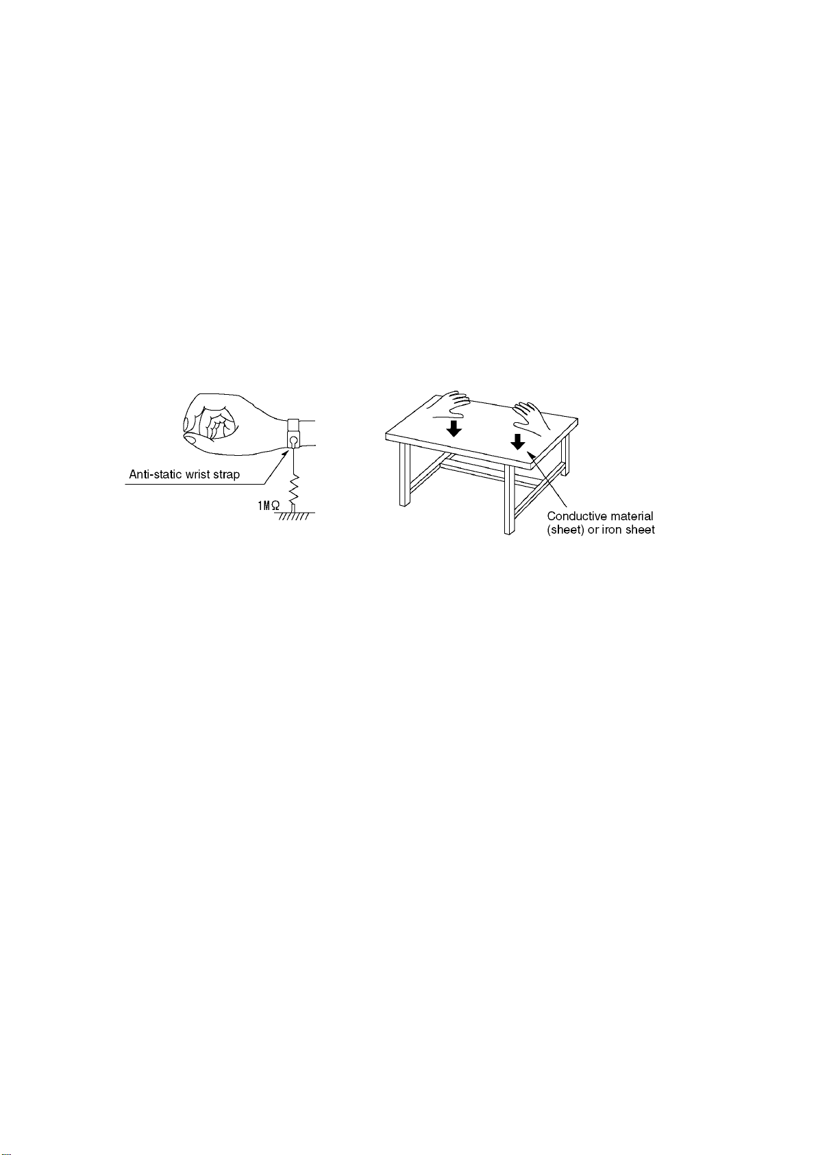
5.1.1. Worktable grounding
5.1.2.Human body grounding
1 Use the anti-static wrist strap to discharge the static electricity form your body.
safety_3 (1577x409x2 tiff)
5.1.3.Handing of optical pickup
1.To keep the good quality of the optical pickup maintenance parts during transportation and before
installation,the both ends of the laser diode are short-circuited.After replacing the parts with new ones,
remove the short circuit according to the correct procedure.(See this Technical Guide).
2.Do not use a tester to check the laser diode for the optical pickup .Failure to do so willdamage the laser
diode due to the power supply in the tester.
5.2.Handing precautions for Traverse Unit (Optical Pickup)
1.Do not give a considerable shock to the traverse unit(optical pickup)as it has an extremely high-precise
structure.
2.When replacing the optical pickup,install the flexible cable and cut is short land with a nipper.See the
optical pickup replacement procedure in this Technical Guide.Before replacing the traverse unit,remove
the short pin for preventingstatic electricity and install a new unit.Connect the connector as short times as
possible.
4.The half-fixed resistor for laser power adjustment cannot be adjusted.Do not turn the resistor.
5
Page 7
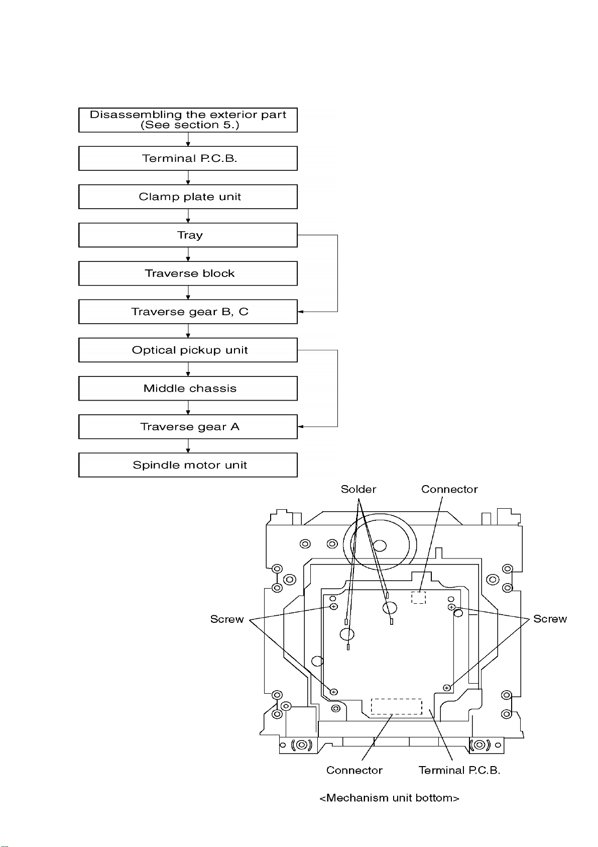
6.ASSEMBLING AND DISASSENBLING THE MECHANISM UNIT
6
6.1Disassembly Procedure
6.2 Terminal P.C.B.
1.Unscrew the screws.
2.Remove the solders.
3.Remove the connectors
5
Page 8
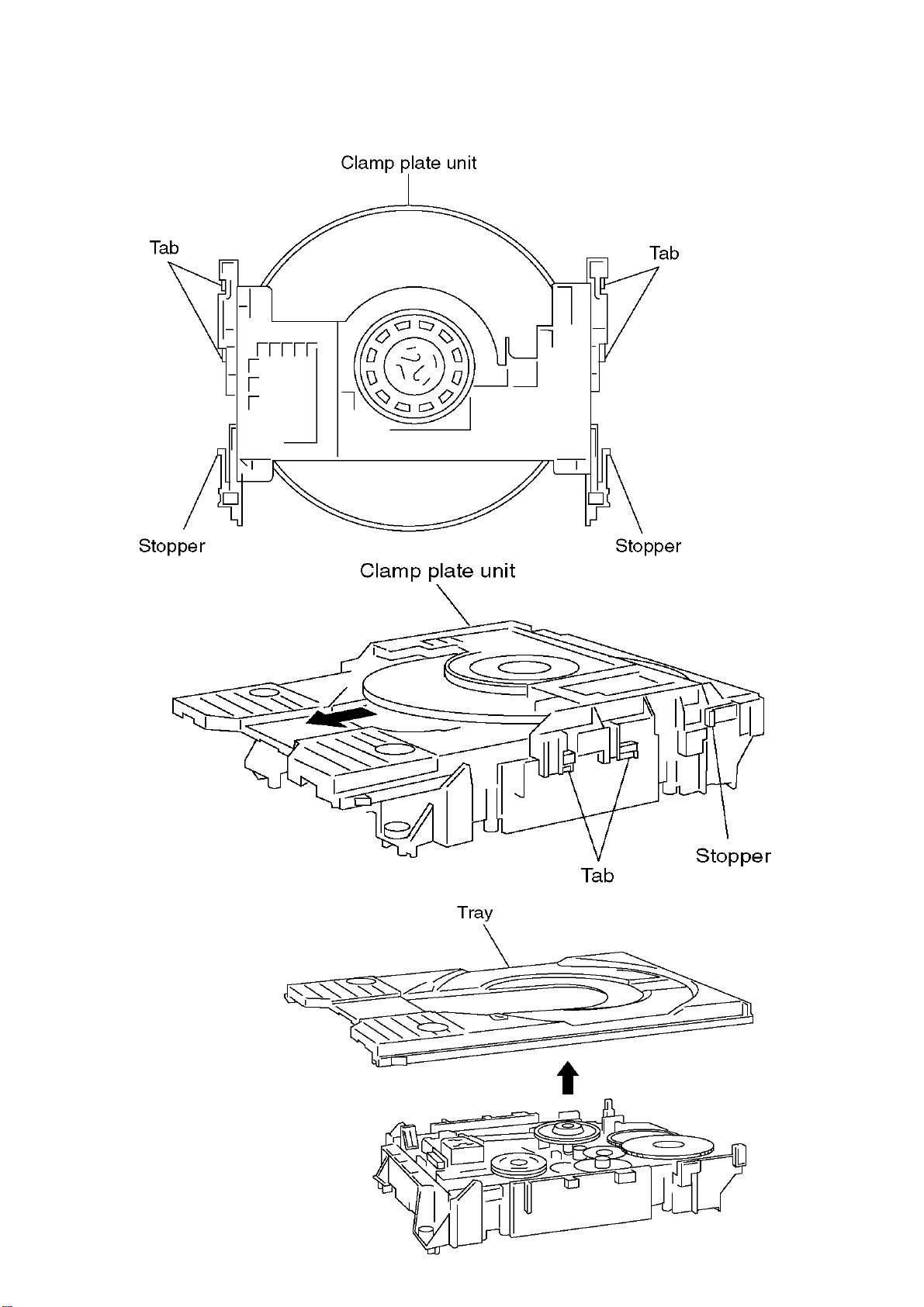
6.3 Clamp Plate Unit
7
1.Spread the stopper with hand to silde the tabs and remove the clamp plate unit.
6.4 Tray
1.Lift the tray.
6
Page 9
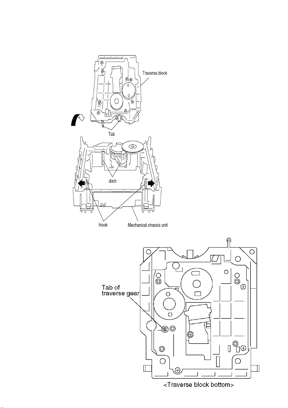
6.5 Traverse Block
8
1.Lift the traverse block while spreading the hook of the mechanical chassis chassis unit.
2.Disengage the tabs from the holes of the mechanical chassis unit.
6.6. Traverse Gear
1.Disengage the tabs from the traverse gear
2.Remove the traverse gears B and C.
7
Page 10
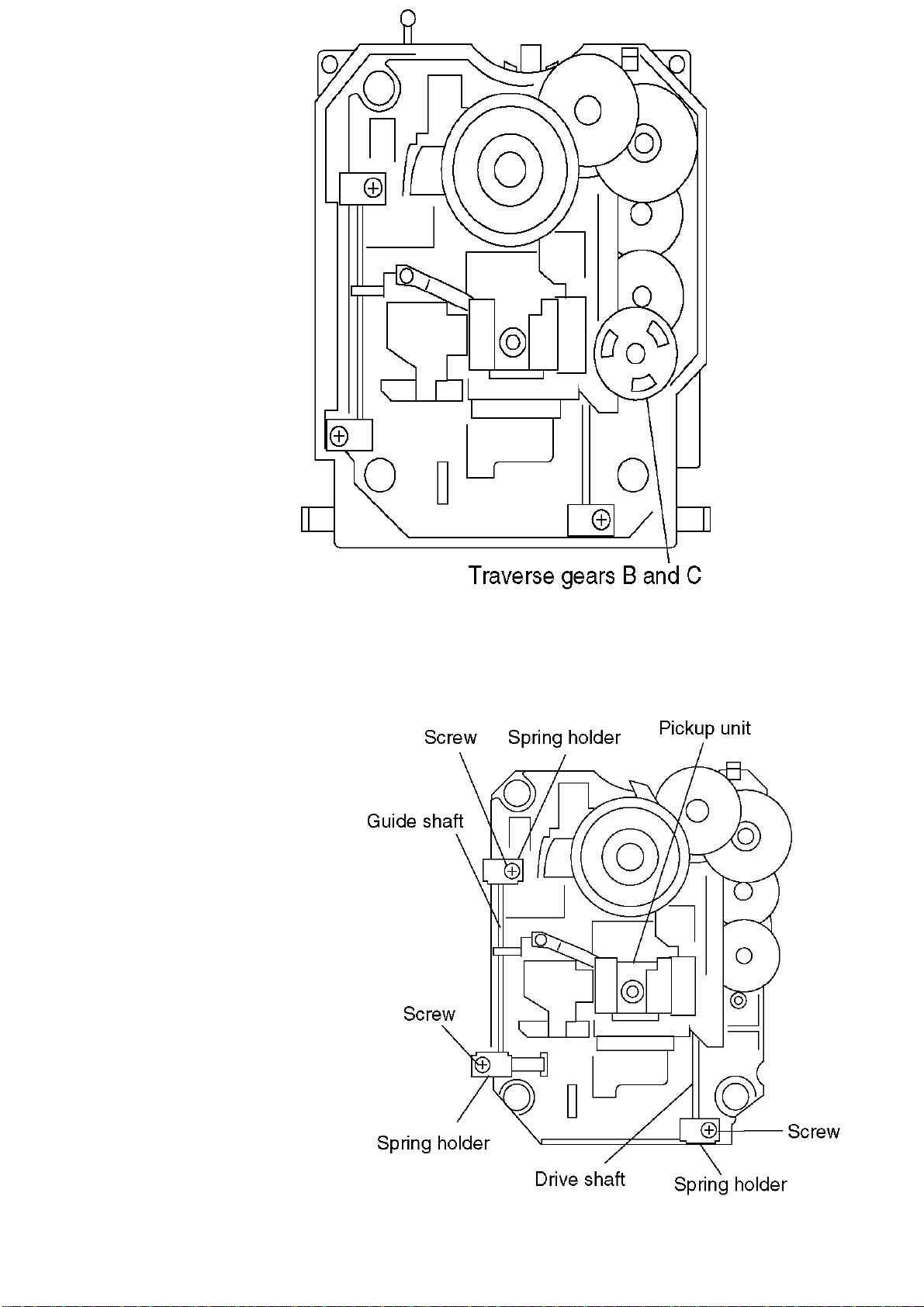
5.6 Mechanism Unit
9
1.Unscrew the screws.
2.Remove the connectors.
6.7. Optical Pickup Unit
1. Unscrew the screws.
5.7 Terninal P.C.B.
2.Remove the spring holders and the springs.
3.Pull out of the drive shaft and guide shaft.
1.Unscrew the screws
2.Remove the solders.
3.Remove the connectors.
6.7.1. Precautions in optical pickup replacement
Page 11
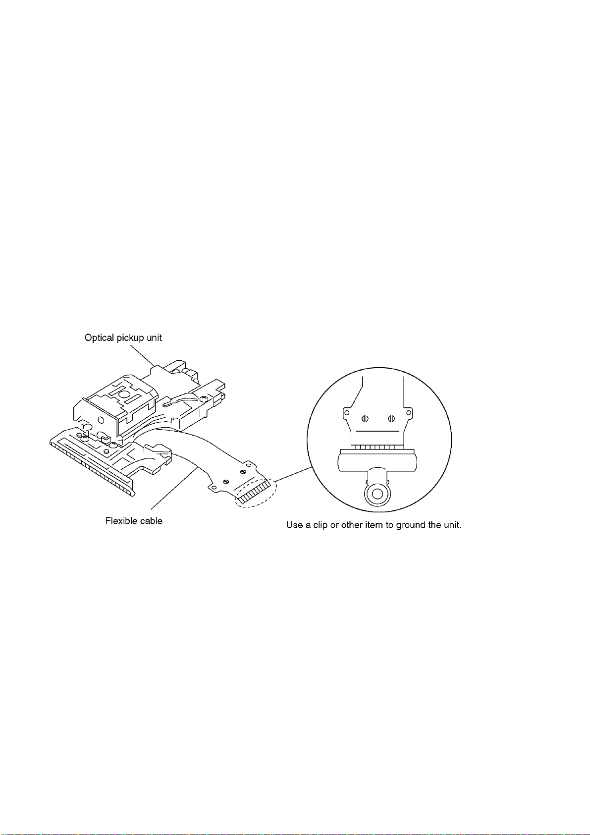
The optical pickup can be damaged by static electricity from you body.Be sure to take static electricity countermeasures
when working around the optical pickup.(Refer to the related page in this Manual about the countermeasures.
3.The use of soldering iron with anti-static feature is recommended when providing short-circuit to laser diode or when
-When using the soldering iron without anti-static feature,short-circuit the flexible cable terminal with a clip before
-After intended repair is finished.remove the solder for short-circuit of laser diode in a correct way following the
procedures described in this Manual.
short-circuiting the land.
10
1.Do not touch laser diode,actuator and their peripheries.
2.Do not use tester to check laser diode.(Laser diode can be damaged easily.)
removing it.
4.Solder the land on flexible cable of optical pickup unit.
Page 12
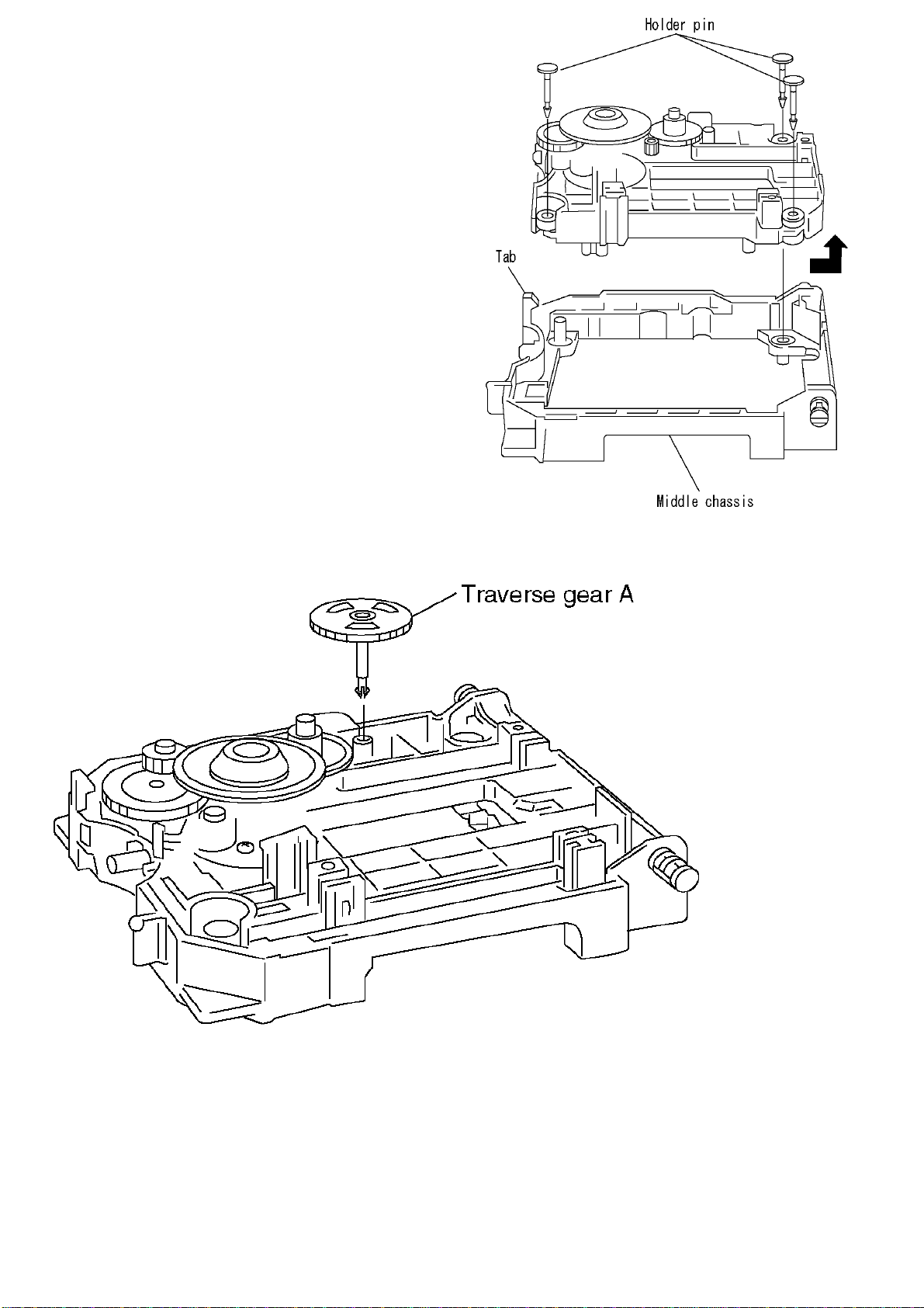
6.8. Disassenbling the Middle Chassis
11
1.Remove the holders pins.
2.Remove the tab.
3.It lifts while pulling it in the direction of the arrow.
6.9. Disassenbling the Traverse Gear A
1.Remove the traverse gear A.
Page 13
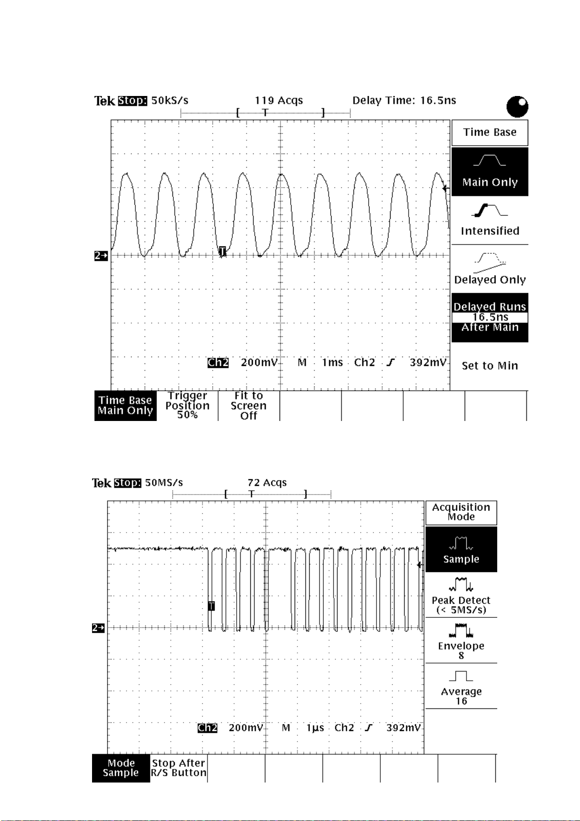
7. Electrical Confirmation
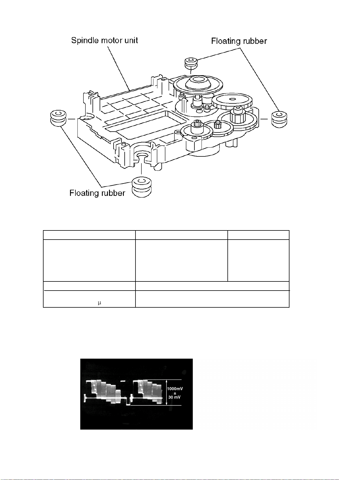
6.10. Disassembling the Sprindle Motor Unit
1.Remove the floating rubbers.
7.1. Video Output (Luminance Signal) Confirmation
DO this confirmation after replacing a P.C.B.
Measurement point
Mode Disc
Color bar 75%
Video output terminal
PLAY(Title 46):DVDT-S15
PLAY(Title 12):DVDT-S01
Measuring equipment,tools
200mV/dir,10 sec/dir
Confirmation value
1000mVp-p±30mV
Purpose:To maintain video signal output compatibility.
1.Connect the oscilloscope to the video output terminal and terminate at 75 ohms.
2.Confirm that luminance signal(Y+S)level is 1000mVp-p±30mV
DVDT-S15
or
DVDT-S01
12
Page 14
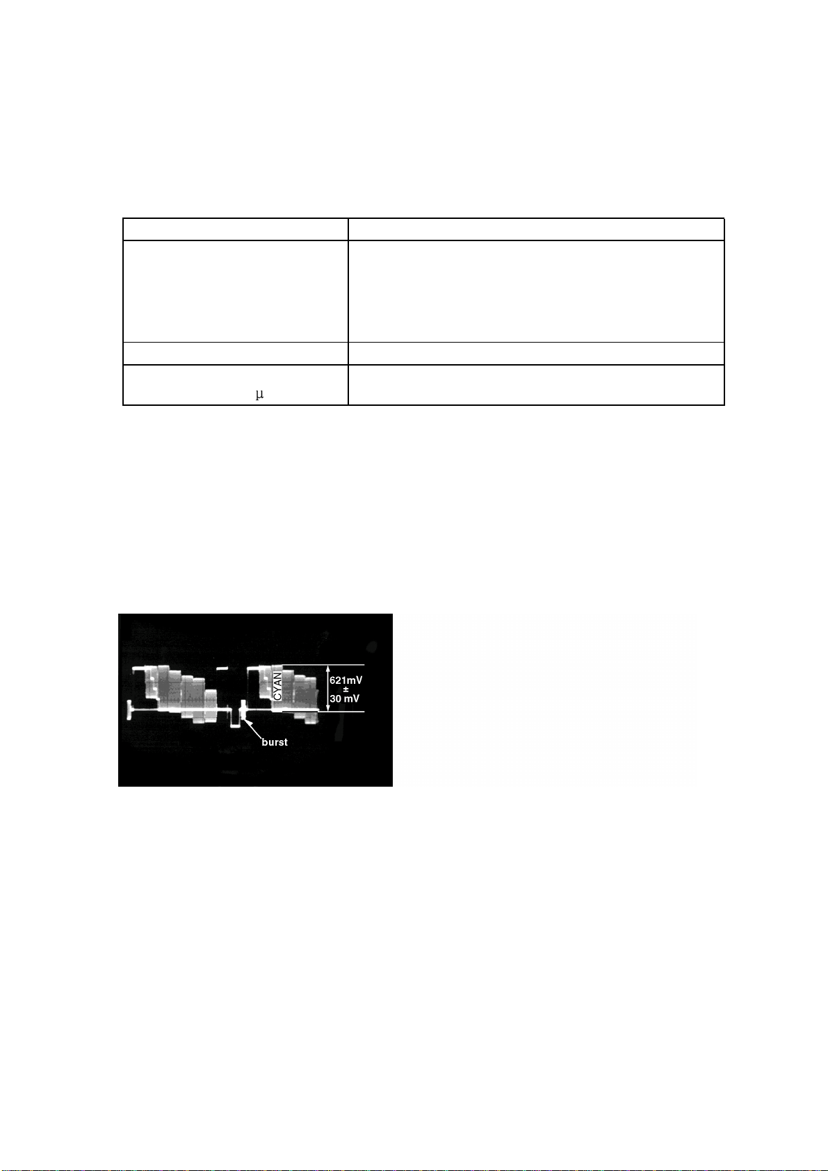
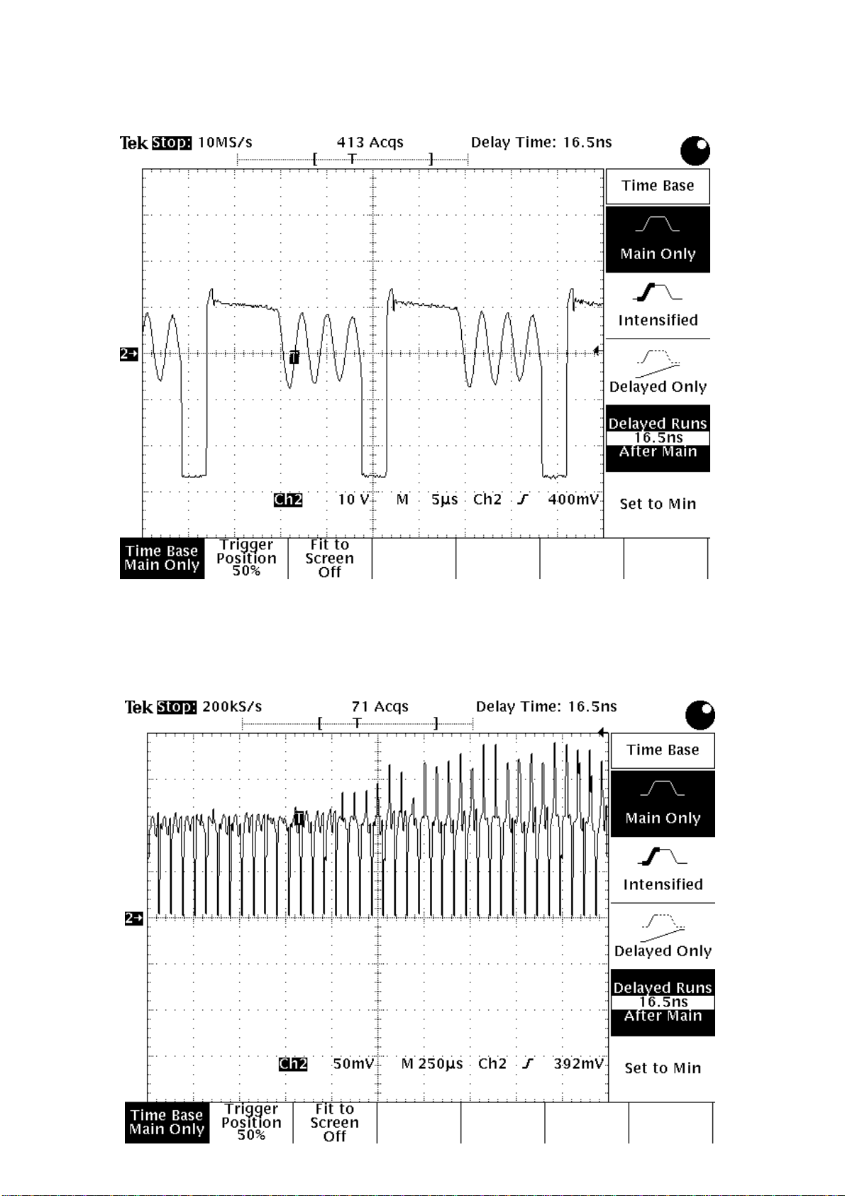
7.2. Video Output (Chrominance Signal) Confirmation
Screwdriver,Oscilloscope
13
Do the confirmation after replacing P.C.B.
Measurement point
Mode Disc
Color bar 75%
Video output terminal
PLAY(Title 46):DVDT-S15
PLAY(Title 12):DVDT-S01
Measuring equipment,tools Confirmation value
200mV/dir,10 sec/dir
621mVp-p±30mV
Purpose:To maintain video signal output compatibility.
1.Connect the oscilloscope to the video output terminal and terminate at 75 ohme.
2.Confirm that the chrominance signal(C)level is 621 mVp-p±30mV
DVDT-S15
or
DVDT-S01
Page 15
8. MPEG BOARD CHECK WAVEFORM
1.X204 WAVEFORM DIAGRAM
2.ZIVA-4.1 PIN.173/STRMCS WAVEFORM DIAGRAM
14
Page 16
3.IC5L0380R PIN.2 WAVEFORM DIAGRAM
4.VIDEO OUPUT WAVEFORM DIAGRAM
15
Page 17

5.ZIVA-4.1PIN.172/DVDREQ WAVEFORM DIAGRAM
16
Page 18

Loader
IC U217 ZIVA-4.1
1 Typical ZiVA-4.1 DVD Decoder Application
9. IC BLOCK DIAGRAM & DESCRIPTION
17
SDRAM
Video Out
Front-End
Chip Set
ZiVA-4.1
ROM
Host
RAM
2 General Description
The ZiVA-4.1 DVD Decoder is the fourth generation in
C-Cube’s ZiVA family of highly integrated, high-performance
DVD decoders for the consumer DVD player market.
The ZiVA-4.1 maintains the same high-level application program interface (API) as earlier decoders. Therefore, system
host code developed for previous products is fully compatible with the ZiVA-4.1 API. This compatibility preserves software investment in designs and will be maintained in future
generations of the decoder family. Figure 2 shows the data
flow of the ZiVA-4.1 Decoder.
Digital Audio Input
2/6/2+6 Channel
Audio DAC
2/6/2+6
Channel
Out
0220c
SDRAM
Interface
Host
Interface
DVD/CD
Interface
Memory
Controller
Host
Interface
Control Logic
SecureView
CSS
Descrambling
Bus Key
Authentication
(optional)
Program
Stream
Decoder
OSD
Decoder
Subpicture
Decoder
MPEG Video
Decoder
CD-DA and LPCM
Decoder
Dolby Digital Audio
Decoder
MPEG Audio
Decoder
Figure 2 ZiVA-4.1 DVD Decoder Data Flow Diagram
Video
Mixer
Audio
DSP
Digital Audio Input
Digital
Video
Encoder
Digital
Audio
Interface
Video
Out
Audio
Interface
0221d
Page 19

A_VSS
3 Pin Descriptions
The ZiVA-4.1 decoder is packaged in a 208-pin Plastic Quad Flat Pack (PQFP) package. Figure 3 shows the
lists the pin number, pin name, and I/O voltage and I/O type.
IC BLOCK DIAGRAM & DESCRIPTION
18
SYSCLK
VCLK
A_VDD
DVD-DATA0/CD-DATA
DVD-DATA1/CD-LRCK
DVD-DATA2/ CD-BC K
DVD-DATA3/CD-C2P0
DVD-DATA4/ CDG-S DATA
DVD-DATA5/CDG-VFSY
DVD-DATA6/CDG-S0S1
DVD-DATA7/CDG-SCLK
VSS
VDD_3.3
VDACK
VREQUEST
VSTROBE
ERROR
VDD_3.3
RESERV ED
VDD_3.3
VSS
HADDR0
HADDR1
HADDR2
RESERV ED
RESERV ED
RESERV ED
VSS
VDD_2.5
RESERV ED
VSS
VDD_3.3
RESERV ED
RESERV ED
RESERV ED
RESERV ED
HDATA7
VSS
HDATA6
HDATA5
HDATA4
HDATA3
HDATA2
VDD_3.3
VSS
HDATA1
HDATA0
VDD_RREF
RREF
VSS_RREF
VDD_VIDEO
VDD_DAC
C/R/V
VSS_VIDEO
VSS_DACNCVDD_ VIDEO
VDD_DAC
Y/B/U
VSS_VIDEO
VSS_DACNCVDD_VIDEO
VDD_DAC
CVBS/G/Y
VSS_VIDEO
VSS_DACNCVDD_VIDEO
VDD_DAC
CVBS + sync
VSS_VIDEO
VSS_DACNCVSS
VDD_2.5
DA-IEC
DA-BCK
DA-XCK
VSS
VDD_3.3
DA-LRCK
DA-DATA0
DA-DATA1
DA-DATA2
DA-DATA3
DAI-DATA
VSS
VDD_3.3
DAI-BCK
DAI-LRCK
RESERVED
RESERVED
RESERVEDNCRESERVEDNCNC
RESERVED
156
155
154
153
152
151
150
149
148
147
146
145
144
143
142
141
140
139
138
137
136
135
134
133
132
131
130
129
128
127
126
125
124
123
122
121
120
119
118
117
116
115
114
113
112
111
110
109
108
107
106
105
157
158
159
160
161
162
163
164
165
166
167
168
169
170
171
172
173
174
175
176
177
178
NC
179
NC
180
NC
181
182
183
184
185
186
187
188
189
190
191
192
193
194
195
196
197
198
199
200
201
202
203
204
205
206
207
CS
208
123456789101112131415161718192021222324252627282930313233343536373839404142434445464748495051
ZiVA-4.1 Decoder
Top View
104
103
102
101
100
99
98
97
96
95
94
93
92
91
90
89
88
87
86
85
84
83
82
81
80
79
78
77
76
75
74
73
72
71
70
69
68
67
66
65
64
63
62
61
60
59
58
57
56
55
54
53
52
MADDR3
MADDR2
MADDR1
VSS
VDD_3.3
MADDR0
MADDR10
SD-BS
SD-CS1/MADDR11
SD-CS0
SD-RAS
VSS
VDD_3.3
SD-CAS
MWE
MADDR4
VSS
VDD_2.5
MADDR5
MADDR6
MADDR7
VSS
VDD_3.3
MADDR8
MADDR9
CLKSEL
SD-CLK
LDQM
MDATA8
VSS
VDD_3.3
MDATA9
MDATA10
MDATA11
MDATA12
MDATA13
VSS
VDD_2.5
MDATA14
VSS
VDD_3.3
MDATA15
MDATA7
MDATA6
MDATA5
MDATA4
MDATA3
MDATA2
VSS
VDD_3.3
MDATA1
MDATA0
RD
R/W
VDD_3.3
NCNCNC
NC
NCNCNC
VSS
INT *
RESET
WAIT*
VDD_3.3
VDD_2.5
NC
VSS
VSS
VDATA0
VDATA1
VDATA2
VDATA3
VDATA4
VDD_3.3
VSS
VSYNC
HSYNC
VDATA5
VDATA6
VDATA7
VSS
VDD_3.3
VDD_2.5
RESERV ED
RESERV ED
RESERV ED
RESERV ED
VSS
PIO0
PIO1
PIO2
PIO3
PIO4
PIO5
PIO6
RESERV ED
VDD_3.3
RESERV ED
RESERV ED
RESERV ED
PIO7
* These pins must be pulled up to 3.3 volts through an external 4.7K resistor
Page 20

Table 1 ZiVA-4.1 Decoder Pin List
IC BLOCK DIAGRAM & DESCRIPTION
19
Table 1 ZiVA-4.1 Decoder Pin List (Continued)
Pin No. Pin Name I/O Voltage I/O Type
1RD
2R/W
3 VDD_3.3 3.3V
4 WAIT 3.3V O, OD, PU
5RESET
6 VSS GROUND
7 VDD_3.3 3.3V —
8INT 3.3V O, OD, PU
9 NC No Connect O
10 NC No Connect O
11 NC No Connect O
12 NC No Connect O
13 VDD_2.5 2.5V
14 VSS GROUND —
15 NC No Connect O
16 NC No Connect O
17 NC No Connect O
18 NC No Connect O
19 VSS GROUND
20 VDD_3.3 3.3V —
21 VDATA0 3.3V O
22 VDATA1 3.3V O
23 VDATA2 3.3V O
24 VDATA3 3.3V O
25 VDATA4 3.3V O
26 VDATA5 3.3V O
27 VDATA6 3.3V O
28 VDATA7 3.3V O
29 VSYNC
30 HSYNC
31 VSS GROUND
32 VDD_3.3 3.3V —
33 RESERVED 3.3V I
34 RESERVED 3.3V I
35 RESERVED 3.3V I
36 VDD_2.5 2.5V
37 VSS GROUND —
38 RESERVED 3.3V I
39 RESERVED 3.3V I
40 RESERVED 3.3V I
41 RESERVED 3.3V I
42 RESERVED 3.3V I
43 PIO0 3.3V I/O
44 VSS GROUND
45 VDD_3.3 3.3V —
46 PIO1 3.3V I/O
47 PIO2 3.3V I/O
48 PIO3 3.3V I/O
3.3V I
3.3V I
—
3.3V I
—
—
—
3.3V I/O
ADV
3.3V I/O
—
—
—
Pin No. Pin Name I/O Voltage I/O Type
49 PIO4 3.3V I/O
50 PIO5 3.3V I/O
51 PIO6 3.3V I/O
52 PIO7 3.3V I/O
53 MDATA0 3.3V I/O
54 MDATA1 3.3V I/O
55 VDD_3.3 3.3V
56 VSS GROUND —
57 MDATA2 3.3V I/O
58 MDATA3 3.3V I/O
59 MDATA4 3.3V I/O
60 MDATA5 3.3V I/O
61 MDATA6 3.3V I/O
62 MDATA7 3.3V I/O
63 MDATA15 3.3V I/O
64 VDD_3.3 3.3V I/O
65 VSS GROUND I/O
66 MDATA14 3.3V I/O
67 VDD_2.5 2.5V
68 VSS GROUND —
69 MDATA13 3.3V I/O
70 MDATA12 3.3V I/O
NCE
71 MDATA11 3.3V I/O
A
72 MDATA10 3.3V I/O
73 MDATA9 3.3V I/O
74 VDD_3.3 3.3V
75 VSS GROUND —
76 MDATA8 3.3V I/O
77 LDQM 3.3V O
78 SD-CLK 3.3V O
79 CLKSEL 3.3V I
80 MADDR9 3.3V O
81 MADDR8 3.3V O
82 VDD_3.3 3.3V
83 VSS GROUND —
84 MADDR7 3.3V O
85 MADDR6 3.3V O
86 MADDR5 3.3V O
87 VDD_2.5 2.5V
88 VSS GROUND —
89 MADDR4 3.3V O
90 MWE
91 SD-CAS
92 VDD_3.3 3.3V
93 VSS GROUND —
94 SD-RAS 3.3V O
95 SD-CS0
96 SD-CS1
/MADDR11 3.3V O
3.3V O
3.3V O
3.3V O
—
—
—
—
—
—
Page 21

Table 1 ZiVA-4.1 Decoder Pin List (Continued)
IC BLOCK DIAGRAM & DESCRIPTION
20
Table 1 ZiVA-4.1 Decoder Pin List (Continued)
Pin No. Pin Name I/O Voltage I/O Type
97 SD-BS
98 MADDR10 3.3V O
99 MADDR0 3.3V O
100 VDD_3.3 3.3V
101 VSS GROUND —
102 MADDR1 3.3V O
103 MADDR2 3.3V O
104 MADDR3 3.3V O
105 RESERVED ANALOG GND
106 NC No connect O
107 NC No connect O
108 RESERVED 3.3V I
109 NC No connect O
110 RESERVED 3.3V I
111 RESERVED 3.3V ANALOG
112 RESERVED 3.3V I
113 DAI-LRCK 3.3V I/O
114 DAI-BCK 3.3V I/O
115 VDD_3.3 3.3V
116 VSS GROUND —
117 DAI-DATA 3.3V I/O
118 DA-DATA3 3.3V O
119 DA-DATA2 3.3V O
120 DA-DATA1 3.3V O
121 DA-DATA0 3.3V O
122 DA-LRCK 3.3V O
123 VDD_3.3 3.3V
124 VSS GROUND —
125 DA-XCK 3.3V I/O
126 DA-BCK 3.3V O
127 DA-IEC 3.3V O
128 VDD_2.5 2.5V
129 VSS GROUND —
130 NC No Connect O
131 VSS_DAC ANALOG GND
132 VSS_VIDEO ANALOG GND —
133 CVBS + sync 3.3V ANALOG O
134 VDD_DAC 3.3V ANALOG O
135 VDD_VIDEO 3.3V ANALOG
136 NC No Connect O
137 VSS_DAC ANALOG GND
138 VSS_VIDEO ANALOG GND —
139 CVBS/G/Y 3.3V ANALOG O
140 VDD_DAC 3.3V ANALOG
141 VDD_VIDEO 3.3V ANALOG —
142 NC No Connect O
143 VSS_DAC ANALOG GND
3.3V O
—
—
—
—
—
ADV
—
—
—
—
—
—
Pin No. Pin Name I/O Voltage I/O Type
144 VSS_VIDEO ANALOG GND —
145 Y/B/U 3.3V ANALOG O
146 VDD_DAC 3.3V ANALOG
147 VDD_VIDEO 3.3V ANALOG —
148 NC No Connect O
149 VSS_DAC ANALOG GND
150 VSS_VIDEO ANALOG GND —
151 C/R/V 3.3V ANALOG O
152 VDD_DAC 3.3V ANALOG
153 VDD_VIDEO 3.3V ANALOG —
154 VSS_RREF ANALOG GND —
155 RREF 3.3V ANALOG O
156 VDD_RREF 3.3V ANALOG
157 A_VSS GROUND —
158 SYSCLK 3.3V I
159 VCLK 3.3V I
160 A_VDD 3.3V ANALOG
161 DVD-DATA0/CD-DATA 3.3V I
162 DVD-DATA1/CD-LRCK 3.3V I
163 DVD-DATA2/CD-BCK 3.3V I
164 DVD-DATA3/CD-C2P0 3.3V I
165 DVD-DATA4/CDG-SDATA 3.3V I
NCE
166 VSS GROUND
A
167 VDD_3.3 3.3V —
168 DVD-DATA5/CDG-VFSY 3.3V I
169 DVD-DATA6/CDG-S0S1 3.3V I
170 DVD-DATA7/CDG-SCLK 3.3V I
171 VDACK 3.3V I
172 VREQUEST 3.3V O
173 VSTROBE 3.3V I
174 ERROR 3.3V I
175 VDD_3.3 3.3V
176 RESERVED GROUND —
177 VDD_3.3 3.3V —
178 VSS GROUND —
179 NC No connect O
180 NC No connect O
181 NC No connect O
182 HADDR0 3.3V I
183 HADDR1 3.3V I
184 HADDR2 3.3V I
185 RESERVED 3.3V I
186 RESERVED 3.3V I
187 RESERVED 3.3V I
188 VSS GROUND
189 VDD_2.5 2.5V —
190 RESERVED 3.3V I
—
—
—
—
—
—
—
—
Page 22

Table 1 ZiVA-4.1 Decoder Pin List (Continued)
IC BLOCK DIAGRAM & DESCRIPTION
21
Table 1 ZiVA-4.1 Decoder Pin List (Continued)
Pin No. Pin Name I/O Voltage I/O Type
191 VSS GROUND —
192 VDD_3.3 3.3V —
193 RESERVED 3.3V I
194 RESERVED 3.3V I
195 RESERVED 3.3V I
196 RESERVED 3.3V I
197 HDATA7 3.3V I/O
198 VSS GROUND
Note: The ZiVA-4.1 core operates at 2.5V ± 10%. Most I/O interface pins can be interfa ced with 3.3-V or 5-V devices depending on the voltage appli ed to the VDD pins associated
with them. Refer to the Application Note for more information.
—
Pin No. Pin Name I/O Voltage I/O Type
199 HDATA6 3.3V I/O
200 HDATA5 3.3V I/O
201 HDATA4 3.3V I/O
202 HDATA3 3.3V I/O
203 HDATA2 3.3V I/O
204 VDD_3.3 3.3V
205 VSS 3.3V —
206 HDATA1 3.3V I/O
207 HDATA0 3.3V I/O
208 CS
3.3V I
—
Signal Descriptions
Table 2 provides the pin name, pin number, type, and description of each signal.
Table 2 ZiVA-4.1 DVD Pin Descriptions
Name Pin No. Ty p e
RESET 5 I Active Low Reset. Assert for at least 5-milliseconds in the presence of clock to
SYSCLK 158 I Optional System Clock. Tie to A_VDD through a 1K Ohm resistor
CLKSEL 79 I Selects SYSCLK or VCLK as clock source. Normal operation is to tie HIGH.
VCLK 159 I System clock that drives internal PLLs and internal DENC. ZiVA-4 requires an
PIO[7:0] 52-46, 43 I/O Programmable I/O pins.
System Services
NC 181-179, 148, 142, 136, 130, 109, 107,
106, 18-15, 12-9
RESERVED 196-193, 190, 187-185, 176, 112, 111, 110,
108, 105, 42-38, 35-33
VDD_3.3 3, 7, 20, 32, 45, 55, 64, 74, 82, 92, 100, 115,
123, 167, 175, 177, 192, 204
VDD_2.5 13, 36, 67, 87, 128, 189 Power 2.5-V supply voltage for core logic
VDD_VIDEO 135, 141, 147, 153 Power 3.3-V Analog Video Power
VDD_DAC 134, 140, 146, 152 Power Analog Video DAC Power
A_VDD 160 Power 3.3-V Analog PLL Power
VDD_RREF 156 Power 3.3V Analog Video Power
VSS 6, 14, 19, 31, 37, 44, 56, 65, 68, 75, 83, 88,
Power and Grounds
VSS_VIDEO 132, 138, 144, 150 Ground Analog Video Ground
VSS_DAC 149, 143, 137, 131 Ground Analog Video DAC Ground
A_VSS 157 Ground Analog PLL Ground
VSS_RREF 154 Ground Video Analog Ground
93, 101, 116, 124, 129, 166, 178, 188, 191,
ADV
198, 205
1
reset the entire chip
Description
NCE
A
external 27-MHz TTL oscillator.
O No connect.
I Tie to VSS or VDD_3.3 as specified in Table 1.
Power 3.3-V supply voltage for I/O signals.
Ground Ground for core logic and I/O signals
Page 23

Table 2 ZiVA-4.1 DVD Pin Descriptions (Continued)
IC BLOCK DIAGRAM & DESCRIPTION
22
Name Pin No. Ty p e
CS 208 I Host chip select. Host asserts CS to select the decoder for a read o r write oper-
HADDR[2:0] 184-182 I Host address bus. 3-bit add ress bus selects one of eight host interface registers.
HDATA[7:0] 197, 199-203, 206, 207 I/O HDATA[7:0] is the 8-bit bi-directional host data bus through which the host
8 O, OD, PU Host interrupt. Open drain signal, must be pulled-up via 4.7kΩ to 3.3 volts.
INT
1 I Read strobe in I mode. Must be held HIGH in M Mode.
RD
Host Interface
2 I Read/write strobe in M mode. Write strobe in I mode. Host asserts R/W LOW
R/W
WAIT
DVD-DATA7/CDG-SCLK 170 I DVD parallel compressed data from DVD DSP. Or CD+G (Subcode) Clock indicat -
DVD-DATA6/CDG-S0S1 169 DVD pa rallel compressed data from DVD DSP. Or CD+G (Subcode) Block Sync
DVD-DATA5/CDG-VFSY 168 DVD parallel compressed data from DVD DSP. Or CD+G (Subcode) Frame Sync
DVD-DATA4/CDG-SDATA 165 DVD parallel compressed data from DVD DSP. Or CD+G (Subcode) data indicat-
DVD-DATA3/CD-C2P0 164 I Asserted HIGH indicates a corrupted byte. Decoder keeps the previous valid pic-
DVD-DATA2/CD-BCK 163 I CD bit clock. Decoder accept multiple BCK rates. This pin is shared with DVD
DVD-DATA1/CD-LRCK 162 I Programmable polarity 16-bit word synchronization to the decoder (right chan-
DVD-DATA0/CD-DATA 161 I Serial CD data. This pin is shared with DVD compressed data DVD-DATA0.
ERROR 174 I Error in input data. If ERROR signal is not available from the DSP it must be
Parallel DVD/CD or Serial CD Interface
VDACK 171 I In synchronous mode , bitstream data acknowledge . Asserted when DVD data is
VREQUEST 172 O Bitstream request. Decoder asserts VREQUEST to indicate that the bitstream
VSTROBE 173 I Bitstream strobe. Programmable dual mode pulse. Asynchronous and synchro-
SD-CAS 91 O Active LOW SDRAM Column Address
SD-RAS
SD-CS0
/MADDR11 96 O Active LOW SDRAM Chip Select 1 or use as MADDR11 for larger SDRAM
SD-CS1
LDQM 77 O SDRAM Lower or Upper Mask
SD-BS
SDRAM Interface
MADDR[10:0] 98, 80, 81, 84-86, 89, 104-102, 99 O SDRAM Address
MDATA[15:0] 63, 66, 69-73, 76, 62-57, 54, 53 I/O SDRAM Data
MWE
SD-CLK 78 O SDRAM Clock
4 O, OD , PU Trans fer not complete / data acknowledge. Active LOW to indicat e host initiated
ADV
94 O Active LOW SDRAM Row Add ress
95 O Active LOW SDRAM Chip Select 0
97 O SDRAM Bank Select
90 O SDRAM Write Enable
1
ation. The falling edge of this signal triggers the read or write operation.
writes data to the decoder Code FIFO. MSB of the 32-bit word is written first.
The host also reads and writes the decoder internal registers and local
SDRAM/ROM via HDATA[7:0].
Driven high for 10 ns before tristate.
to select Write and LOW to select Read for M Mode only.
transfer is not complete. WAIT
serted when decoder is ready to complete transfer cycle. Open drain signal,
must be pulled-up via 1kΩ to 3.3 volts. Driven high for 10 ns before tristate.
ing subcode data clock input or output.
indicating block-start synchronization input.
indicating frame-start or composite synchronization input.
ing serial subcode data input.
NCE
ture on-screen until the next valid picture is decoded. This pin is shared with
A
DVD compressed data DVD-DATA3.
compressed data DVD-DATA2.
nel HIGH). This pin is shared with DVD compressed data DVD-DATA1.
grounded.
valid. Polarity is programmable.
input buffer has available space. Polarity is programmable.
nous. In Asynchronous mode, an external source pulses VSTROBE to indicate
data is ready for transfer. In synchronous mode, VSTROBE clocks data.
(64 Mbits).
Description
is asserted after the falling edge of CS and reas-
Page 24

Table 2 ZiVA-4.1 DVD Pin Descriptions (Continued)
IC BLOCK DIAGRAM & DESCRIPTION
23
Name Pin No. Ty p e
C/R/V 151 Analog O DAC video output format. Macrovision encoded.
Y/B/U 145 Analog O DAC video output format. Macrovision encoded.
CVBS/G/Y 139 Analog O DAC video output format. Macrovision encoded.
CVBS + sync 133 Analog O DAC video output format: Composite + sync. Macrovision encoded.
RREF 155 Analog O Reference Resistor. Connecting to pin 154 through a 1.18K+/- 1% resistor is rec-
Analog Video Output
VCLK 159 I System clock that drives internal PLLs. ZiVA-4 requires an external 27-MHz TTL
HSYNC 30 I/O Horizontal sync. The decoder begins outputting pixel data for a new horizontal
VCLK 159 I Video clock. Clocks out data on input. VDATA[7:0]. Clock is typically 27 MHz.
VDATA[7:0] 28-21 O Video data bus. Byte serial CbYCrY data synchronous with VCLK. At power-up,
29 I/O Vertical sync. Bi-directional, the decoder outputs the top border of a new field
VSYNC
Digital Video Output
DA-DATA[3:0] 118, 119, 120, 121 O PCM Data Out. Eight channels. Serial audio samples relative to DA_BCK and
DA-BCK 126 O PCM Bit Clock. Divided by 8 from DA_XCK. DA_BCK can be either 48 or 32 times
DA-LRCK 122 O PCM Left Clock. Identifies the channel for each sample. The polarity is program-
DA-XCK 125 I/O Audio External Frequency Clock input or output. DA_BCK and DA_LRCK are
Audio Interface
DA-IEC 127 O PCM data out in IEC-958 format or compressed data out in IEC-1937 format.
DAI-DATA 117 I PCM data input.
DAI-BCK 114 I PCM input bit clock.
DAI-LRCK 113 I PCM left/right clock.
Digital Mic In
1. I - input, O - output, OD - open drain, PU - requires external pull-up resistor.
ADV
1
ommended
oscillator.
line after the falling (active) edge of HSYNC
the decoder does not drive VDATA. During boot-up, the decoder uses configuration parameters to drive or 3-state VDATA.
on the first HSYNC
synchronization or top/bottom field notification from an external source.
(VSYNC
DA_LRCK.
the sampling frequency
mable
NCE
derived from this clock. DA_XCK can be 384 or 256 times the sampling fre-
A
quency
Description
.
after the falling edge of VSYNC. VSYNC can accept vertical
HIGH = bottom field. VSYNC LOW = Top field)
Table 3 lists the pins that have Schmitt Trigger inputs when programmed as inputs.
Table 3 Schmitt Trigger Inputs
Pin No. Pin Name Pin No. Pin Name
173 VSTROBE 165 DVD-DATA4/CDG-SDATA
171 VDACK 168 DVD-DATA5/CDG-VFSY
174 ERROR 169 DVD-DATA6/CDG-S0S1
161 DVD-DATA0/CD-DATA 170 DVD-DATA7/CDG-SCLK
162 DVD-DATA1/CD-LRCK 5 RESET
163 DVD-DATA2/CD-BCK 29 VSYNC
164 DVD-DATA3/CD-C2P0 30 HSYNC
Page 25

IC BLOCK DIAGRAM & DESCRIPTION
IC U204 CY37032
24
UltraLogicTM 32-Macrocell ISRTM CPLD
Features
• 32 macrocells in two logic blocks
• In-Sy stem Reprogrammable™ (ISR™)
—JTAG-compliant on-board pr ogramming
—Design changes don’t cause pinout changes
—Design changes don’t cause timing changes
•Up to 32 I/Os
—Plus 5 dedicated inputs including 4 clock inputs
• High speed
= 222 MHz
—f
MAX
= 5.0 ns
—t
PD
—t
S
—t
CO
• Product-term clo cking
• IEEE 1149.1 JTAG boundary scan
• Programmable slew rate control on individual I/Os
• Low power option on individual logic block basis
• 5V and 3.3V I/O capability
• User-Programmable Bus Hold capabilities on all I/Os
• Simple Timing Model
• PCI compl iant
• Available in 44-Lead TQFP and PLCC packages
• Pinout compatible with the CY37032V, CY37064/
CY37064V, CY7C371i
= 3.0 ns
= 4.0 ns
Logic Block Diagram
−
I/O
I/O
0
Pin Configurations
I/O
/TCLK
5
I/O
6
I/O
7
CLK2/I
0
JTAG
EN
GND
CLK0/I
1
I/O
8
I/O
9
I/O
10
I/O
11
44-Lead PLCC (J67)
65 34 2
7
8
9
10
11
12
13
14
15
16
17
18
19 20 2221 23 24 2726 2825
12
I/O
/TMS
I/O
Clock/
Input
Input
1
4
4
16 I/Os 16 I/Os
15
LOGIC
BLOCK
A
36
16
PIM
16
36
LOGIC
BLOCK
16
B
16
Top View
0
31
I/O2GND
I/O3I/O4I/O1I/O
14
CC
V
I/O15I/O
13
CCO
V
1
44
43 42 4041
16
GND
28
I/O29I/O30I/O
I/O
I/O27/TDI
39
I/O
38
26
I/O
25
37
I/O
24
36
CLK1/I
35
34
33
32
31
30
29
20
I/O
I/O18I/O17I/O
/TDO
19
I/O
GND
I
3
CLK3/I
I/O
23
I/O
22
I/O
21
37032-2
4
2
I/O5/TCLK
I/O
I/O
CLK2/I
JTAG
GND
CLK
I/O
I/O
I/O
I/O
0
44 43 42 4041 39 38 37 3536 34
1
6
2
3
7
4
0
5
EN
6
/I
7
1
8
8
9
9
10
10
11
11
12
I/O
TDI
TCLK
TMS
4
44-Lead TQFP (A44)
Top
View
0
I/O2GND
I/O3I/O4I/O1I/O
18 19 20 222113 14 15 171612
14
CC
V
GND
I/O15I/O
/TMS
13
I/O
JTAG Tap
Controller
JTAG
EN
−
I/O
I/O
16
31
CCO
V
16
28
I/O29I/O30I/O31I/O
33
32
31
30
29
28
27
26
25
24
23
37032–3
20
I/O
I/O18I/O17I/O
/TDO
19
I/O
I/O27/TDI
I/O
26
I/O
25
I/O
24
CLK1/I
GND
I
3
CLK3/I
I/O
23
I/O
22
I/O
21
TDO
37032-1
4
2
Selection G uide
CY37032-222 CY37032-200 CY37032-154 CY37032-125
Maximum Propagation Delay, tPD (ns) 5.0 6.0 7.5 10
Minimum Set-Up, tS (ns) 3.0 4 5 5.5
Maximu m Cl o ck to O u tp u t, t
T ypic al Supply Current, ICC (mA) in Low Power Mode 15 15 15 15
Shaded areas contain advance information.
(ns) 4.0 4 4.5 6.5
CO
Page 26

Electrical Characteristics
IC BLOCK DIAGRAM & DESCRIPTION
25
Over the Ope rating Range
Parameter Description Tes t Condi tions Min. Typ. Max. Unit
V
V
V
V
V
I
IX
I
OZ
OH
OHZ
OL
IH
IL
Output HIGH Voltage VCC = Min. IOH = –3.2 mA
(Com’l/Ind)
Output HIGH Voltage with Output Disabled
[6]
VCC = Max. IOH = 0 µA (Com’l)
IOH = 0 µA (Ind)
IOH = –50 µA (Com’l)
IOH = –100 µA (Ind)
Output LOW Voltage VCC = Min. IOL = 16 mA (Com’l/Ind)
Input HIGH Voltage Guaranteed Input Logical HIGH v oltage
for all input s
Input LOW Voltage Guaranteed In put Logical LOW voltage
for all input s
[4]
[4]
[2]
[3]
[3]
[3]
[3]
[2]
Input Load Current VI = GND OR VCC, Bushold Disabled
Output Leakage Current VO = GND or VCC, Output Disabled,
2.4 V
4.0 V
4.3 V
3.6 V
3.6 V
0.5 V
2.0 V
−0.5
−10
−50
CCmax
0.8 V
10
50
Bushold Disabl ed
I
OZBH
I
OS
I
BHL
Output Leakage Current VCC = Max., VO = 3.3V, Output
Disabled
Outp u t S h ort Circui t
[5, 6]
Current
Input Bus Ho ld LOW Sus taining
VCC = Max., V
VCC = Min., VIL = 0.8V +75
[3]
, Bus-Hold Enabled
= 0.5V
OUT
0
−30 −160
−70 −125 µA
Current
I
BHH
Input Bus Hold HIGH
VCC = Min., VIH = 2.0V
−75 µA
Sustaining Current
I
BHLO
Input Bus Hold LO W Over driv e
VCC = Max. +500
Current
I
BHHO
Input Bus Hold HIGH Overdriv e
VCC = Max. -500
Current
V
µA
µA
mA
µA
µA
µA
Inductance
[6]
Parameter Description Test Conditions 44-Lead TQFP 44-Lead PLCC Unit
L Maximum Pin Inductance VIN = 5.0V at f = 1 MHz 2 5 nH
Capacitance
[6]
Parameter Description Test Conditions Max. Unit
C
I/O
C
CLK
Endurance Characteristics
Input/Output Capacit ance VIN = 5.0V at f = 1 MHz at TA = 25°C 8 pF
Clock Signal Capacitance VIN = 5.0V at f = 1 MHz at TA = 25°C 12 pF
[6]
Parameter Description T est Conditions Min. Typ. Unit
N Minimum Reprogramming Cycles Normal Programming Conditions
Notes:
2. I
= –2 mA, IOL = 2 mA for TDO.
OH
3. When the I/O is output disabled, the bus-hold circuit can weakly pull the I/O to a maximum of 4.0V if no leakage current is allowed. This voltage is lowered
significantly by a small leakage current. Note that all I/Os are output disabled during ISR programming. Refer to the application note “Unde rst and i ng B us H old ”
for additional information.
4. These are absolute values with respect to device ground. All overshoots due to system or tester noise are included.
5. Not more than one output should be tested at a time. Duration of the short circuit should not exceed 1 second. V
problems caused by tester ground degradation.
6. Tested initially and after any design or process changes that may affect these parameters.
[1]
1,000 10,000 Cycles
= 0.5V has been chosen to avoid test
OUT
Page 27

2 Megabit (256 K x 8-Bit)
IC BLOCK DIAGRAM & DESCRIPTION
IC U214 Am29F002B/Am29F002NB
26
CMOS 5.0 Volt-only Boot Sector Flash Memory
DISTINCTIVE CHARACTERISTICS
■ Single power supply operation
— 5.0 Volt-only operation for read, erase, and
program operations
— Minimizes system level requirements
■ Manufactured on 0.32 µm process technology
— Compatible with 0.5 µm Am29F002 device
■ High performance
— Access times as fast as 55 ns
■ Low power consumption (typical values at
5 MHz)
— 1 µA standby mode current
— 20 mA read current
— 30 mA program/erase current
■ Flexible sector architecture
— One 16 Kbyte, two 8 Kbyte, one 32 Kbyte, and
three 64 Kbyte sectors
— Supports full chip erase
— Sector Protecti on features:
A hardware method of locking a sector to
prevent any program or erase operations within
that sector
Sectors can be loc k ed v ia pr ogr ammi ng eq uipme nt
T emporary Sector Unprotect feat ure allows code
changes in previously locked sectors
■ Top or bottom boot block co nfigurations a vaila ble
■ Embe dded Algorithms
— Embedded Erase algorithm automatically
preprograms and erases the entire chip or any
combination of designated sectors
— Embedded Progr am algorithm automatically
writes and verifies data at specified addresses
■ Minimum 1,000,000 write cycle guarantee per
sector
■ 20-year data retention at 125°C
— Reliable operation for the life of the system
■ Package option
— 32-pin PDIP
— 32-pin TSOP
— 32-pin PLCC
■ Compatibility with JEDEC standards
— Pinout and software compatible with
single-power supply Flash
— Superior inadvertent write protection
■ Data# Pol ling and toggle bits
— Provides a software method of detecting
program or erase operation completion
■ Erase Suspend/Erase Resume
— Suspends an erase oper ation to read data from,
or program data to, a sector that is not being
erased, then resumes the erase operation
■ Hardware reset pin (RESET#)
— Hardw are method to reset the device to reading
array data (not available on Am29F002NB)
Page 28

PRODUCT SELECTOR GUIDE
IC BLOCK DIAGRAM & DESCRIPTION
27
Family Part Number Am29F002B/Am29F002NB
= 5.0 V ± 5% -55
V
Speed Option
Max access time, ns (t
Max CE# access time, ns (t
Max OE# access time, ns (t
CC
= 5.0 V ± 10% -70 -90 -120
V
CC
)557090120
ACC
)557090120
CE
) 30303550
OE
Note: See “AC Characteristics” for full specifications.
BLOCK DIAGRAM
V
CC
V
SS
RESET#
n/a Am29F002NB
Sector Switches
Erase Voltage
Generator
DQ0
–
DQ7
Input/Output
Buffers
WE#
CE#
OE#
A0–A17
State
Control
Command
Register
VCC Detector
PGM Voltage
Generator
Timer
Chip Enable
Output Enable
STB
Logic
Address Latch
Y-Decoder
X-Decoder
STB
Data
Latch
Y-Gating
Cell Matrix
Page 29

CONNECTION DIAGRAMS
IC BLOCK DIAGRAM & DESCRIPTION
28
RESET#
NC
A16
A15
A12
A7
A6
A5
A4
A3
A2
A1
A0
DQ0
DQ1
DQ2
V
SS
NC on Am29F002NB
1
2
3
4
5
6
7
8
9
10
11
12
13
14
15
16
PDIP
32
31
30
29
28
27
26
25
24
23
22
21
20
19
18
17
V
CC
WE#
A17
A14
A13
A8
A9
A11
OE#
A10
CE#
DQ7
DQ6
DQ5
DQ4
DQ3
A7
A6
A5
A4
A3
A2
A1
A0
DQ0
5
6
7
8
9
10
11
12
13
14
A12
4
DQ1
15
A15
3
DQ2
A16
2
PLCC
17
SS
V
NC on Am29F002NB
RESET#
VCCWE#
31 30
1
32
19 2016
18
DQ3
DQ4
DQ5
A17
29
28
27
26
25
24
23
22
21
DQ6
A14
A13
A8
A9
A11
OE#
A10
CE#
DQ7
NC on Am29F002NB
A11
A9
A8
A13
A14
A17
WE#
V
CC
RESET#
A16
A15
A12
A7
A6
A5
A4
1
2
3
4
5
6
7
8
9
10
11
12
13
14
15
16
Standard TSOP
32
31
30
29
28
27
26
25
24
23
22
21
20
19
18
17
OE#
A10
CE#
DQ7
DQ6
DQ5
DQ4
DQ3
V
SS
DQ2
DQ1
DQ0
A0
A1
A2
A3
Page 30

PIN CONFIGURATION
IC BLOCK DIAGRAM & DESCRIPTION
29
A0–A17 = 18 addresses
DQ0–DQ7 = 8 data inputs/outputs
CE# = Chip enable
OE# = Output enable
LOGIC SYMBOL
18
A0–A17
8
DQ0–DQ7
WE# = Write enable
RESET# = Hardware reset pin, active low
(not available on Am29F002NB)
= +5.0 V single power supply
V
CC
(see Product Selector Guide for
device speed ratings and voltage
supply tolerances)
V
SS
= Device ground
NC = Pin not connected internally
CE#
OE#
WE#
RESET#
N/C on Am29F002NB
Page 31

4 Banks x 1M x 16Bit Synchronous DRAM
IC BLOCK DIAGRAM & DESCRIPTION
IC U206 SDRAM-HY57V65162B
30
DESCRIPTION
The Hyundai HY57V651620B is a 67,108,864-bit CMOS Synchronous DRAM, ideally suited for the Mobile applications which require low power consumption and extended temperature range. HY57V651620B is organized as 4banks
of 1,048,576x16.
HY57V651620B is offering fully synchronous operation referenced to a positive edge of the clock. All inputs and outputs are synchronized with the rising edge of the clock input. The data paths are internally pipelined to achieve very
high bandwidth. All input and output voltage levels are compatible with LVTTL.
Programmable options include the length of pipeline (Read latency of 2 or 3), the number of consecutive read or write
cycles initiated by a single control command (Burst length of 1,2,4,8 or Full page), and the burst count
sequence(sequential or interleave). A burst of read or write cycles in progress can be terminated by a burst terminate
command or can be interrupted and replaced by a new burst read or write command on any cycle. (This pipelined
design is not restricted by a `2N` rule.)
FEATURES
• Single 3.3V ± 10% power supply
• All device pins are compatible with LVTTL interface
• JEDEC standard 400mil 54pin TSOP-II with 0.8mm
of pin pitch
• All inputs and outputs referenced to positive edge of
system clock
• Data mask function by UDQM or LDQM
• Internal four banks operation
ORDERING INFORMATION
Part No. Clock Frequency Power Organization Interface Package
HY57V651620BTC-7I 143MHz
HY57V651620BTC-75I 133MHz
HY57V651620BTC-10SI 100MHz
HY57V651620BLTC-7I 143MHz
HY57V651620BLTC-75I 133MHz
HY57V651620BLTC-10SI 100Mhz
Normal
Power
• Auto refresh and self refresh
• 4096 refresh cycles / 64ms
• Programmable Burst Length and Burst Type
- 1, 2, 4, 8 or Full page for Sequential Burst
- 1, 2, 4 or 8 for Interleave Burst
• Programmable CAS Latency ; 2, 3 Clocks
power
4Banks x 1Mbits
x16
Lower
LVTTL 400mil 54pin TSOP II
This document is a general product description and is subject to change without notice. Hyundai Electronics does not assume any
responsibility for use of circuits described. No patent licenses are implied.
Rev. 0.4/Nov.00
Page 32

PIN CONFIGURATION
IC BLOCK DIAGRAM & DESCRIPTION
31
VDD
DQ0
VDDQ
DQ1
DQ2
VSSQ
DQ3
DQ4
VDDQ
DQ5
DQ6
VSSQ
DQ7
DD
V
LDQM
/WE
/CAS
/RAS
/CS
BA0
BA1
A10/AP
A0
A1
A2
A3
DD
V
1
2
3
4
5
6
7
8
9
10
11
12
13
14
15
16
17
18
19
20
21
22
23
24
25
26
27
54pin TSOP II
400mil x 875mil
0.8mm pin pitch
VSS
54
DQ15
53
VSSQ
52
DQ14
51
DQ13
50
VDDQ
49
DQ12
48
DQ11
47
VSSQ
46
DQ10
45
DQ9
44
VDDQ
43
DQ8
42
SS
V
41
NC
40
UDQM
39
CLK
38
CKE
37
NC
36
A11
35
A9
34
A8
33
A7
32
A6
31
A5
30
A4
29
SS
V
28
PIN DESCRIPTION
PIN PIN NAME DESCRIPTION
CLK Clock
CKE Clock Enable
CS Chip Select Enables or disables all inputs except CLK, CKE and DQM
BA0,BA1 Bank Address
A0 ~ A11 Address
RAS, CAS, WE
LDQM, UDQM Data Input/Output Mask Controls output buffers in read mode and masks input data in write mode
DQ0 ~ DQ15 Data Input/Output Multiplexed data input / output pin
VDD/VSS Power Supply/Ground Power supply for internal circuits and input buffers
VDDQ/VSSQ Data Output Power/Ground Power supply for output buffers
NC No Connection No connection
Row Address Strobe,
Column Address Strobe,
Write Enable
The system clock input. All other inputs are registered to the SDRAM on the
rising edge of CLK
Controls internal clock signal and when deactivated, the SDRAM will be one
of the states among power down, suspend or self refresh
Selects bank to be activated during RAS activity
Selects bank to be read/written during CAS activity
Row Address : RA0 ~ RA11, Column Address : CA0 ~ CA7
Auto-precharge flag : A10
RAS, CAS and WE define the operation
Refer function truth table for details
Page 33

FUNCTIONAL BLOCK DIAGRAM
I/O Buffer & Logic
IC BLOCK DIAGRAM & DESCRIPTION
32
1Mbit x 4banks x 16 I/O Synchronous DRAM
Self refresh logic
CLK
CKE
CS
RAS
CAS
WE
UDQM
LDQM
& timer
Row active
State Machine
refresh
Column
Active
Internal Row
counter
Row
Pre
Decoders
Column
Pre
Decoders
1Mx16 Bank 3
X decoders
1Mx16 Bank 2
X decoders
X decoders
1Mx16 Bank 1
1Mx16 Bank 0
X decoders
Y decoders
Memory
Cell
Array
Sense AMP & I/O Gate
DQ0
DQ1
DQ14
DQ15
Bank Select
A0
A1
A11
BA0
BA1
Address buffers
Address
Registers
Mode Registers
Column Add
Counter
Burst
Counter
CAS Latency
Data Out Control
Pipe Line Control
Page 34

ABSOLUTE MAXIMUM RATINGS
IC BLOCK DIAGRAM & DESCRIPTION
33
Parameter Symbol Rating Unit
Ambient Temperature TA -40 ~ 85 °C
Storage Temperature TSTG -55 ~ 125 °C
Voltage on Any Pin relative to VSS VIN, VOUT -1.0 ~ 4.6 V
Voltage on VDD relative to VSS VDD, VDDQ -1.0 ~ 4.6 V
Short Circuit Output Current IOS 50 mA
Power Dissipation PD 1 W
Soldering Temperature ⋅ Time TSOLDER 260 ⋅ 10 °C ⋅ Sec
Note : Operation at above absolute maximum rating can adversely affect device reliability
DC OPERATING CONDITION (TA= -40 to 85°C)
Parameter Symbol Min Typ. Max Unit Note
Power Supply Voltage VDD, VDDQ 3.0 3.3 3.6 V 1
Input High Voltage VIH 2.0 3.0 VDDQ + 2.0 V 1,2
Input Low Voltage VIL VSSQ - 2.0 0 0.8 V 1,3
Note :
1.All voltages are referenced to VSS = 0V
2.VIH (max) is acceptable 4.7V AC pulse width with ≤3ns of duration
3.VIL (min) is acceptable -2.0V AC pulse width with ≤3ns of duration
AC OPERATING CONDITION (TA= -40 to 85°C, VDD=3.3V ± 0.3V, VSS=0V)
Parameter Symbol Value Unit Note
AC Input High / Low Level Voltage VIH / VIL 2.4/0.4 V
Input Timing Measurement Reference Level Voltage Vtrip 1.4 V
Input Rise / Fall Time tR / tF 1 ns
Output Timing Measurement Reference Level Voutref 1.4 V
Output Load Capacitance for Access Time Measurement CL 50 pF 1
Note :
1. Output load to measure access time is equivalent to two TTL gates and one capacitor (50pF)
For details, refer to AC/DC output circuit
Page 35

! 3-Termainal Regulators
IC WS7805
POSITIVE-VOLTAGE REGULATORS
25
V
)
WS7805DP
TO-220
WS7805CV
O
C
I
TO-252
IC BLOCK DIAGRAM & DESCRIPTION
34
! Output Current Up to 1.5 A
! No External Components
! Internal Thermal Overload Protection
! High Power Dissipation Capability
! Internal Shot-Circuit Current Limiting
! Output Transistor Safe-Area
Compensation
DESCRIPTION
This series of fixed-voltage monolithic integrated-circuit
voltage regulators designed for a wide range of
applications. These applications include on-card
regulation for elimination of noise and distribution
problems associated with single-point regulation. Each
of these regulators can deliver up to 1.5 amperes of
output current. The internal current limiting and thermal
shutdown features of these regulators make them
O
C
I
(TO-252)
essentially immune to overload.
ABSOLUTE MAXIMUM RATINGS OVER OPERATING TENPERATURE
RANGE (UNLESS OTHERW ISE NOTE
WS7805 PARAMETER UNIT
Input voltage, V
Continuous total dissipati on at 25℃ free-air temperature
Lead temperature 1.6mm (1/16 inch) from case 10 seconds 260
Storage temperature range, T
I
stg
RECOMMEMDED OPERATING CONDITIONS
Input voltage, V
Output current, I
Operating virtual junction temperature, T
I
O
J
35 V
2W
-65 to 150
MIN MAX UNIT
7
1.5 A
070
℃
℃
℃
Page 36

35
10. Decode Board Block Diagram
Mixed Separate Dolby
2CH
S Complex Video
LPF
5.1CH
UDE
ITERFACE
BUFFER
MIC INPUT
ANALOG SIGNALS
STRMREQ
DSTROBE
STRMDMA
エョ
ソレ
8 Bit Data
CY37032
CS4228
I2S
DVDREQ CSTROBE
RAS/CAS
Simulate video
output
8 Bit host interface
LPF
ZiVA 4.1
27MHz
OSC
SDRAM
1 16Mbits
16 ホサ
SDRAM
1 16Mbits
REMOTE INPUT
V8000
3 LINE
OUTPUR FRONT
FLASH
DRAM
MMORY
I2C
DECODE BOARD DIAGRAM
Page 37

VFD401
11 SCHEMATIC & P.C.B WIRING DIAGRAM
FRONT SCHEMATIC DIAGRAM
11.1
36
P10
P11
P12
P13
P14
P15
P16
SEG8
SEG7
SEG6
SEG5
SEG4
SEG3
SEG2
SEG1
VCC
13
14S115S216S317S418S519S620S721S822
FIL+
1
F1
2
F1
5G
4G
3G
2G
1G
NC
NC
NC
NC
NC
P1
P2
P3
P4
P5
P6
P7
P8
P9
F2
F2
GRID1
4
GRID2
5
GRID3
6
GRID4
7
GRID5
8
9
10
11
12
13
SEG16
14
SEG15
15
SEG14
16
SEG13
17
SEG12
18
SEG11
19
SEG10
20
SEG9
21
SEG8
22
SEG7
23
SEG6
24
SEG5
25
SEG4
26
SEG3
27
SEG2
28
SEG1
29
31
FIL-
32
SEG9
SEG10
SEG11
SEG12
-25V
SEG13
SEG14
SEG15
SEG16
GRID5
23
S9
24
S10
25
S11
26
S12/G1
27
VEE
28
S13/G1
29
S14/G9
30
S15/G8
31
S16/G7
32
G6
33
G5
UPD16312
G434G335G236G137VDD38LED439LED340LED241LED142VSS43OSC
GRID4
GRID3
GRID2
GRID1
U401
VCC
VDD
GND
R413
33K
C404
101
C405
104
KEY4
KEY3
KEY2
KEY1
R414
33K
C407
100uF/16V
VFDCK
VFDAT
C403
101
3
1
2
R417
10K
VCC
U403
HS0038A2
101
KEY312KEY4
KEY2
KEY1
STB
CLK
VSS
DIN
DO
SW4
SW3
SW2
SW1
44
R405
33K
C401
104
R401
R402
11
R403
10
R404
9
VFDST
8
7
GND
6
5
4
3
2
1
SW4
SW3
SW2
MSW
33K
33K
33K
33K
VCC C406
R411
R412
33K
VCC
10K
10K
10K
10K
10K
33K
IR
R415
100
R416
10K
R406
R407
R408
R409
R410
VCC
C402
100uF/16V
VFD-32
KEY1
KEY2
KEY3
KEY4
SEG1
1N4148
K401
K402
K403 K411
D401
K405
K406
K407
K408K404
SEG2
1N4148
D402
K409
K410
K412
SEG3
1N4148
D403
K413
K414
K415
K416
SEG4
1N4148
D404
FIL+
R418
100
VCC
GND
-25V
FIL-
IR
GND
VFDST
VFDCK
VFDAT
XS401
1
2
3
4
5
XS05
XS402
1
2
3
4
5
XS05
Page 38

FRONT P.C.B. WIRING DIAGRAM
37
11.2
Page 39

MIC601
P.W. & OK. SCHEMATIC DIAGRAM
38
11.3
OK
R609 10K
TC606
R603
560R
C603
103
R604
560R
C604
103
R607
1K
R608
1K
TC605
22uF/16V
9MIC602
8
7
6
5
4
3
2
1
9
8
7
6
5
4
3
2
1
L602
L601
TC601
4.7uF
R601
22K
TC602
4.7u
R602
22K
22uF/16V
C605 101P
TC603
4.7uF/16V
2
3
R605
10k
+9VA 3
6
5
R606
10K
8 4
U601A
4558
R610
10K
C606
101P
U601B
4558
1
TC604
4.7uF/16V
7
13
VR602
10K
R618
10K
VR601
10K
R613
24K
C607 100P
-9VA
R612
4.7K
2
R611
4.7K
R623
10K
2
+9VA
1
U602A
4558
8 4
TC613
4.7uF/16V
R614
1K
C608
102
R617
100K
+5V
R615
100K
R616
1K
VD601
1N4148
VD603
VD602
1N4148
1N4158
TC611
47uF/16V
VOICE-DET
R620
6.8K
6
5
U602B
4558
R619
7
330
+9V +9VA -9V -9VA
R621
10ohm1/6W
TC615
100uF/25V
C601
104
R622
10ohm1/6W
TC616
100uF/25V
C602
104
Page 40

D501 D504
P.W. & OK. SCHEMATIC DIAGRAM
11.4
39
D502 D503
BCN502
SW-SPST
!
L502
! !
BC501
~400V 102
!
L501
!
!
!
!
F501
T1.6A/250V
!
~400V 102
~400V 102
BCN501
~220V
!
BC502
BC503
C502
47uF/400V
BC505
~275V 104
BC504
~275V 104
RV501
14D471
R505
470K 2W
R501
82K/2W
3
VCC
U501
5L0380R
L504
C510
101
D507
HER105
C511
101
D510
HER105
D511
HER105
C537
101
D512
HER105
C538
101
D509
SR560
C512
C536
D508
HER105
C525
220uF/16V
D505
10ohm
47uF/50V
C507
223
R503
C509
R507
270K/2W
D506
HER105
C506
101
!
T501
2
3
4
8
7
!
U502
2501
BC506
~400V 222
!
17
18
15
16
13
14
12
11
10
R502
10K/2W
C503
101/1KV
L503
FB
2
4
FB
D
1
GND
C505
104
R504
1M
C504
103/1KV
HER107
10uH/1A
C501
470uF/25V
L505
10uH/2A
C516
470uF/25V C517
L506 10uH/2A
C519
1000uF/16V
C522
330uF/25V
C524
100uF/50V
L507
10uH/1A
330
R509
U503
LM431A
470uF/25V
R514
1K
K
A
C514
470uF/25V
D513
IN4001
C520
1000uF/16V
C521
330uF/25V
C527
104
R512
R
10K
R510
10K
R513
4.7K
ZD501
5.1V
S+12V
DGND
DGND
S+5V
VOICE-DET
+9V
L508
FB
+5V
OK
AGND
+9V
-9V
DGND
DGND
+5V
+5V
+5V
DGND
-21V
FLFL+
1
2
3
4
1
2
3
4
5
6
7
8
9
5
4
3
2
1
XS502
XS04
C528
470uF/16V
CN501
XS05
CN503
XS09
DGND
SD+5V
DGND
SA+5V
DGND
S+8V
1
6
5
4
3
CN502
2
XS06
1
3
OUT
SA+5V
C508
100uF/16V
IN
GND
U504
LM7805
2
Page 41

40
P.W. & OK. WIRING DIAGRAM
11.5
Page 42

D+5V
MIAN SCHEMATIC DIAGRAM
11.6
41
R201 10K
TC201
10uF/16V
XS201
XS05
5
4
3
2
1
VD202
1N4148
D+5V
TXD
RXD
R210
47K
CPUCLK27
CLKOUTA
P+5V D+5V
L201
FB
/CPU_RST
Q211
R240
10K
R219
4.7K
C212
150pF
R258
R204
R214
R207
R208
DATA
A17
A15
A14
A13
A12
A11
A10
A9
U205E
HC14
33ohm
33ohm
33ohmCLKSER
33ohm
33ohm
S9015
P+5V
R209
47K
SDA
CS MSCK
/RD /RD1
R213
75ohm
1011
R202
33ohm
DATA
R257
0ohm
CLKOUTA1
P+5V
C202
104
C203
104
/CPU_RST
/WR1/WR
AD[15..0]
P+5V
R253
4.7K
R228 33ohm
R252 33ohm
1
SDEN1
2
SDEN0
3
SCLK
4
BHE/ADEN
5
WR
6
RD
7
ALE
8
ARDY
9
S2
10
S1
11
S0
12
GND0
13
X1
14
X2
15
VCC0
16
CLKOUTA
17
CLKOUTB
18
GND1
19
A19
20
A18
21
VCC1
22
A17
23
A16
24
A15
25
A14
26
A13
27
A12
28
A11
29
A10
30
A9
AD7
AD13
AD14
AD15
CSADAC
C201
104
R249
33ohm
MTXD
93
94
95
96
97
98
99
100
UZI
AD7
TXD
RXD
AD15
SDATA
S6/CLKDIV2
AM186EM-33KC
A831A732A633A534A435A336A237VCC238A139A040GND241WHB42WLB43HLDA44HOLD45SRDY46NMI47DT/R48DEN49MCS0
PA2
PA3
PA4
R21533ohm
R21633ohm
R21733ohm
92
AD14
PA1
R21833ohm
91
AD6
VCC5
U201
88
90
GND589AD13
AD5
AD12
86
87
AD12
AD11
85
AD4
84
AD11
MNMI
AD3
AD10
83
INT3/INTA1/IRQ
R220
33ohm
AD3
AD4
AD5
AD6
AD2
AD9
82
AD981AD2
AD10
TMRIN0
TMROUT0
TMROUT1
TMRIN1
MCS3/RFCH
PCS5/A1
PCS6/A2
LCS/ONCE0
UCS/ONCE1
INT1/SELECT
INT2/INTA0
50
AD1
AD8
AD0
DRQ0
DRQ1
RES
GND4
MCS2
VCC4
PCS0
PCS1
GND3
PCS2
PCS3
VCC3
INT0
INT4
MCS1
C204
104
80
79
78
77
76
75
74
73
72
71
70
69
68
67
66
65
64
63
62
61
60
59
58
57
56
55
54
53
52
51
R222
33ohm
R221
33ohm
P+5V
C205
TC203
104
47uF/16V
AD1
AD8
AD0
STRMDMA
SCK
/MSYSRST
/MLDR_RST
/CPU_RST
MCSADAC
/MROMACS
/MSTRMCS
/MDVDCS
/MLCS
/MUCS /UCS
DVDINT
/LDRRDY
MATN_FM
D-MUTE
R239 33ohm
R238 33ohm
R237 33ohm
R233
R231
R232
R230 33ohm
R229 33ohm
R250
R227
R225
1K
D-MUTE
33ohm
33ohm
33ohm
0ohm
33ohm
R241 47K
R242 47K
/SYSRST
/LDRRST
MCS2
/ROMACS
/STRMCS
/DVDCS
LCS
VOICE-DET
MCS1
R226
1K
AD0
AD1
JP201
JP202
STRMDMA
SCK
/SYSRST
MCS2
/ROMACS
/STRMCS
/DVDCS
LCS
/UCS
VCK
VSYNC
VDATA7
VDATA6
VDATA5
VDATA4
VDATA3
VDATA2
VDATA1
VDATA0
FBSMT
FBSMT
D+3V D+5V
0R
0R
+9V D+5V
0R
0R
FB
FB
FB
FB
FB
FB
FB
FB
FB
DSTROBE
STRMERR
FB
/DECSEL
FB
RXD
FB
/HOSTRDY/H-RDY
FB
FB
FB
VOUT/G
YOUT/B
COUT/R
ROUT
LOUT
SDD7
SDD5SDD6
SDD3SDD4
SDD1SDD2
DSTROBE
STRMERR
/DECSEL
D+5V
S1_AD0
R248
S1_AD1
DACK
XSTRMREQ
/HOSTSEL
TXD
U205A
HC14
R247
/LDRRST
SDD0
22K
22K
XS207
XS05
XS206
XS15
HSYNC
FB
L256
FB
L257
FB
L258
FB
L259
FB
L260
FB
L261
FB
L262
FB
L263
FB
L264
FB
L265
12
1
2
3
4
5
1
2
3
4
5
6
7
8
9
10
11
12
13
14
15
XS205
XS20
1 2
3 4
5 6
7 8
9 10
11 12
13 14
15 16
17 18
19 20
21 22
XS202
XS22
2122
1920
1718
1516
1314
1112
3.3V
D+5V
GND
SDA
CLKSER
D+5V
GND
GND
GND
GND
GND
GND
SCLOCK
SDATA
910
78
56
34
12
R2105
R2106
R2107
R2165
L219
L227
L228
L229
L239
L274
L273
L272
L271
L270
L269
L268
L267
L266
L202
L203
L204
A[3..1]
A[15..1]
/DVDWAIT
/DVDWAIT
XS203
XS05
To VFD board
1
2
3
4
5
L249
L250
L251
L252
L253
FB
IR
GND
FB
CS
FB
FB
SCK
FB
DATA
TC202
10uF/16V
D+5V
IR 5 6
IR
A1
A2A3A4A5A6A7A8
/DVDINT
/DVDINT
U205C
HC14
U205D
89
HC14
R223
33ohm
R224
0ohm
Page 43

MADDR[11..0]
MIAN SCHEMATIC DIAGRAM
42
MDATA]15..0]
C209
102
LA[19..16]
D+5V
L255
FBSMT
C210
102
PWR-U214
R254
0ohm
C215
104
TC240
47uF/16V
A1
A2
A3
A4
A5
A6
A7
A8
A9
A10
A11
A12
A13
A14
A15
LA16
LA17
LA18
/UCS
/RD
/WR
/CPU_RST
U214
AM29F800BT-120SC
11
A0
10
A1
9
A2
8
A3
7
A4
6
A5
5
A6
4
A7
42
A8
41
A9
40
A10
39
A11
38
A12
37
A13
36
A14
35
A15
34
A16
3
A17
1
NC
12
/CE
14
/OE
43
/WE
44
/RESET
PWR-U214 PWR_HST_DRAM
LA19
LA18
LA17
LA16
/ROMACS
CLKOUTA
/CPU_RST
/RD
/STRMCS
STRMDMA
R212
100ohm
L238
FB
U206
1
VCC0
D+5V
10
11
13
14
15
16
17
18
19
20
21
22
23
24
25
VD214
1N5401
/RD
MCS2
MCS1
/WR
LCS
2
3
4
5
6
7
8
9
C228
104
L206
FBSMT
DQ0
DQ1
GND0
DQ2
DQ3
VCC1
DQ4
DQ5
GND1
DQ6
DQ712DQ8
VCC2
DQML
WE
CAS
RAS
CS
BA
A10
A0
A1
A2
A3
VCC3
SDRAM-2X512KX16-8A
C229
104
VD215
1N5401
/RD
MCS2
MCS1
/WR
LCS
MDATA0
15
D0
D1
D2
D3
D4
D5
D6
D7
D8
D9
D10
D11
D12
D13
D14
D15
A18
/BYTE
VCC
GND1
GND2
1
I/O5
2
I/O6
3
I/O7
4
CLK2/10
5
JTAG
6
GND
7
CLK0/11
8
I/O8
9
I/O9
10
I/O10
11
I/O11
AD0
17
AD1
19
AD2
21
AD3
24
AD4
26
AD5
28
AD6
30
AD7
16
AD8
18
AD9
20
AD10
22
AD11
25
AD12
27
AD13
29
AD14
31
AD15
2
A18-U220 LA19
33
23
13
32
44
U204
CY37032-QFP44
I/O1212I/O1313I/O1414I/O1515VCC16GND17I/O1618I/O1719I/O1820I/O1921I/O20
R255
0ohm
C213
1000pF
R234
37
39
I/O040I/O141I/O242I/O343I/O4
VCC38GND
CLK1/14
CLK3/12
22
C217
0.1uF
I/O2834I/O2935I/O3036I/O31
I/O27
I/O26
I/O25
I/O24
GND
I/O23
I/O22
I/O21
13
PWR-U214
33ohm
33
32
31
30
29
28
27
26
25
24
23
TC237
47uF/16V
U205B
HC14
3 4
7 14
RXD
DSTB
STRMRQ
/DECSEL
/HOSTSEL
CSTROBE
DVDREQ
DACK
SDD7
SDD6
SDD5
SDD4
SDD3
SDD2
SDD1
SDD0
/H-RDY
D+5V
R246
750ohm
C206
104
R235
0ohm
R236
33ohm
SDD[7..0]
DSTROBE
XSTRMREQ
MDATA1
MDATA2
MDATA3
MDATA4
MDATA5
MDATA6
MDATA7 MDATA8
/SD_CS1
MADDR11
MADDR10
MADDR0
MADDR1
MADDR2
MADDR3 MADDR4
SD_CLK
L/UDQM
/MWE
/SD_CAS
/SD_RAS
/SD_CS0
ZV+5V D+3V
50
GND5
49
48
47
46
45
44
43
42
41
40
39
38
37
36
35
34
33
32
31
30
29
28
27
26
C232
104
10
11
12
13
14
15
16
17
18
19
20
C219
102
MDATA15
MDATA14
MDATA13
MDATA12
MDATA11
MDATA10
MDATA9
MADDR9
MADDR8
MADDR7
MADDR6
MADDR5
C233
104
TC207
47uF/16V
U208
424260-70
1
VCC1
2
D0
3
D1
4
D2
5
D3
6
VCC2
7
D4
8
D5
9
D6
D7
NC1
NC2
WE
RAS
NC3
A0
A1
A2
A3
VCC3
C220
102
GND3
D15
D14
D13
D12
GND2
D11
D10
NC4
CASL
CASH
GND1
C221
102
40
39
38
37
36
35
34
33
32
D9
31
D8
30
29
28
27
OE
26
A8
25
A7
24
A6
23
A5
22
A4
21
DQ15
DQ14
GND4
DQ13
DQ12
VCC5
DQ11
DQ10
GND3
DQ9
VCC4
NC1
DQMU
CLK
CKE
NC0
A9
A8
A7
A6
A5
A4
GND2
C231
C230
104
104
PWR_HST_DRAM
AD0
AD1
AD2
AD3
AD4
AD5
AD6
AD7
A1
A3
A5
A7 A9
L207
FB
AD8
AD9
AD10
AD11
AD12
AD13
AD14
AD15
MCS2
MCS1
A17
A15
A13
A11
TC204
47uF/16V
MDATA0
MDATA1
MDATA2
MDATA3
MDATA4
MDATA5
MDATA6
MDATA7 MDATA8
MADDR11
MADDR10
MADDR0
MADDR1
MADDR2
MADDR3 MADDR4
D+3V
U207
1
VCC0
2
DQ0
3
DQ1
4
GND0
5
DQ2
6
DQ3
7
VCC1
8
DQ4
9
DQ5
10
GND1
11
DQ6
DQ712DQ8
13
VCC2
14
DQML
15
WE
16
CAS
17
RAS
18
CS
19
BA
20
A10
21
A0
22
A1
23
A2
24
A3
25
VCC3
SDRAM-2X512KX16-8A
SDRAM0 PWR
C234
C235
104
104
D+3V
C226
104
GND5
DQ15
DQ14
GND4
DQ13
DQ12
VCC5
DQ11
DQ10
GND3
DQ9
VCC4
NC1
DQMU
CLK
CKE
NC0
A9
A8
A7
A6
A5
A4
GND2
C236
104
TC205
47uF/10V
C237
104
2
50
49
48
47
46
45
44
43
42
41
40
39
38
37
36
35
34
33
32
31
30
29
28
27
26
C238
104
U211
AS2815
IN3GND1OUT
TC206
47uF/10V
MDATA15
MDATA14
MDATA13
MDATA12
MDATA11
MDATA10
MDATA9
MADDR9
MADDR8
MADDR7
MADDR6
MADDR5
C239
104
ZV+5V
C227
104
AD[7..0]
AD7
AD6
AD5
AD4
AD3
AD2
AD1
AD0
A[19..0]
/HOSTRDY
Page 44

TC209
MIAN SCHEMATIC DIAGRAM
43
47uF/16V
D+3V
STRMERR
A[3..1]
AD[7..0]
/DVDCS
/RD
/WR
/DVDWAIT
/SYSRST
/DVDINT
C246
104
D+3V
C223
104
C247
104
STRMERR CSTROBE
R266
VDD-RREF
RREF
VSS-RREF
VDD-DAC3
C/R/V
VSS-DAC3
NC14
VDD-DAC2
Y/B/U
VSS-DAC2
NC13
VDD-DAC1
CVBS/G/Y
VSS-DAC1
NC12
VDD-DAC0
VSS-DAC0
NC11
VSS16
VDD254
DA-IEC
DA-BCK
DA-XCK
VSS15
VDD3312
DA-LRCK
DA-DATA0
DA-DATA1
DA-DATA2
DA-DATA3
DAI-DATA
VSS14
VDD3311
DAI-BCK
DAI-LRCK
NC10
NC9
NC8
D+3V
1K
156
155
154
153
152
151
150
149
148
147
146
145
144
143
142
141
140
139
138
137
136
135
134
133
132
131
130
129
128
127
126
125
124
123
122
121
120
119
118
117
116
115
114
113
112
111
110
109
108
107
106
105
L212
VDD-RREF
R267
1.18K/1%
VGND
VCK
ZV-AVCC
TC214
47uF/16V
VGND
AVCC-ENC
VID_C
VID_Y
VID_COMP
R271
R272
R273
R274
R275
R276
R277
DAI_DATA
FB
TC213
47uF/16V
TC212
47uF/16V
C245
104
C224
104
C248
104
R262
4.7K
C244
104
C274
104
C249
104
D+3V
C243
104
C250
104
R263
1K
C242
104
D+3V
C251
104
/DVDCS
/RD
/WR
/DVDWAIT
/SYSRST
/DVDINT
C241
104
VDATA0
VDATA1
VDATA2
VDATA3
VDATA4
VDATA5
VDATA6
VDATA7
VSYNC
HSYNC
C252
104
D+2.5V
C240
104
C253
104
1
2
3
4
5
6
7
8
9
10
11
12
13
14
15
16
17
18
19
20
21
22
23
24
25
26
27
28
29
30
31
32
33
34
35
36
37
38
39
40
41
42
43
44
45
46
47
48
49
50
51
52
MDATA[15..0]
MADDR[11..0]
C254
104
L/UDQM
SD_CLK
/SD_CS1
/SD_CS0
/SD_RAS
/SD_CAS
/MWE
C255
104
RD
R/W
VDD330
WAIT
RESET
VSS0
VDD331
INT
NC0
NC1
NC2
NC3
VDD250
VSS1
NC4
NC5
NC6
NC7
VSS2
VDD332
VDATA0
VDATA1
VDATA2
VDATA3
VDATA4
VDATA5
VDATA6
VDATA7
VSYNC
HSYNC
VSS3
VDD333
RESERVED0
RESERVED1
RESERVED2
VDD251
VSS4
RESERVED3
RESERVED4
RESERVED5
RESERVED6
RESERVED7
PIO0
VSS5
VDD334
PIO1
PIO2
PIO3
PIO4
PIO5
PIO6
PIO7
C256
104
172
173
174
ERROR
VDD3314
VSTROBE
R289
33R
MADDR4
C258
104
DACK
SDD5
SDD6
SDD7
166
167
168
169
170
171
VDACK
VREQUEST
R288
33R
VSS17
VDD3313
DVD-DATA6/CDG-S0S1
DVD-DATA5/CDG-VFSY
DVD-DATA7/CDG-SCLK
R28533R
R28633R
R287
33R
C259
C260
104
104
SDD3
SDD4
164
165
DVD-DATA3/CD-C2PO
DVD-DATA4/CDG-SDATA
SD-BS97MADDR1098MADDR099VDD3310
96
R28333R
R28433R
MADDR11
C261
104
SDD[7..0]
AD0
AD1
AD2
AD3
AD4
AD5
AD6
AD7
192
193
194
195
196
197
198
199
200
201
202
203
204
205
206
207CS208
HDATA4
HDATA3
MDATA4
MDATA5
MDATA6
HDATA6
HDATA5
MDATA7
MDATA15
VSS21
HDATA7
RESERVED21
TC210
47uF/16V
RESERVED18
RESERVED19
RESERVED20
MDATA13
MDATA14
VSS22
HDATA2
HDATA1
HDATA0
VDD3317
MDATA053MDATA154VDD33555VSS656MDATA257MDATA358MDATA459MDATA560MDATA661MDATA762MDATA1563VDD33664VSS765MDATA1466VDD25267VSS868MDATA1369MDATA1270MDATA1171MDATA1072MDATA973VDD33774VSS975MDATA876LDQM77SD-CLK78CLKSEL79MADDR980MADDR881VDD33882VSS1083MADDR784MADDR685MADDR586VDD25387VSS1188MADDR489MWE90SD-CAS91VDD33992VSS1293SD-RAS94SD-CS095SD-CS1/MADDR11
MDATA0
MDATA1
MDATA2
MDATA3
L/UDQM
SD_CLK
/SD_CS1
/SD_CS0
/SD_RAS
/SD_CAS
/MWE
190
191
VSS20
VDD3316
RESERVED17
MDATA11
MDATA12
D+3V
187
188
189
VSS19
VDD255
RESERVED16
MDATA9
MDATA10
VD213
1N4001
183
184
185
186
HADDR2
RESERVED14
RESERVED15
R295
R296
MDATA8
33R
33R
A1A2A3
181
182
NC17
HADDR0
HADDR1
R294
33R
MADDR9
178
179
180
NC15
NC16
U217
ZIVA-4.1
R293
33R
MADDR8
R264
4.7K
177
VSS18
VDD3315
R29233R
33R
MADDR7
C257
104
176
R291
MADDR6
175
RESERVED13
R290
33R
MADDR5
R265
4.7K
SDD0
SDD1
SDD2
157
158
159
160
161
162
163
VCLK
A-VSS
A-VDD
SYSCLK
DVD-DATA2/CD-BCK
DVD-DATA0/CD-DATA
DVD-DATA1/CD-LRCK
VSS13
MADDR1
MADDR2
MADDR3
100
101
102
103
104
R28233R
R28133R
R28033R
R27933R
R27833R
MADDR0
MADDR1
MADDR2
D+2.5V
C262
104
MADDR3
TC211
47uF/10V
MADDR10
VDD-VIDEO3
VSS-VIDEO3
VDD-VIDEO2
VSS-VIDEO2
VDD-VIDEO1
VSS-VIDEO1
VDD-VIDEO0
CVBS+SYNC
VSS-VIDEO0
RESERVED12
RESERVED11
RESERVED10
RESERVED9
RESERVED8
DVDREQ
C268
104
C267
104
C263
104
R268
R269
75ohm
75ohm
VGND
33R
33R
22R
33R
33R
33R
33R
D+5V
C2149
104
U218A
1 2
HCU04
R2110
4.7K
X204
27MHz
C293
20P
FBSMT
FBSMT
R259
220
L211
L210
C264
104
R270
75ohm
C269
102
C265
104
VID_C
VID_Y
VID_COMP
IEC958
DA_BCK
DA_XCK
DA_LRCK
DA_DATA1
DA_DATA2
DA_DATA3
R2170
R211
U218B
HCU04
3 4
C294
20P
CSTROBE
DVDREQ
VCK
D+3V
33ohm
33ohm
714
C266
104
L209
FBSMT
L208
FBSMT
IEC958
DA_BCK
DA_XCK
DA_LRCK
DA_DATA1
DA_DATA2
DA_DATA3
DAI_DATA
CPUCLK27
VCK
D+3V
Page 45

JK202
MIAN SCHEMATIC DIAGRAM
44
V-OUT5
GREEN
BLUE
RED
JK202
S-VIDEO
WHITE
JK201
V-OUT2
7
15
LUMA
CHROMA
1 2
5
6
Power Connector
R2100
10K
FBSMT
FBSMT
FBSMT
FBSMT
FB
FB
VOICE-DET
L243
FBSMT
VGND
Q202
2SC1815-Y
TC215
100uF/16V
OKA
AGND
Q203
1015
AGND
L220
FB
VD205
1N4148
R2103
10K
C270
104
MUTE-1
C271
104
1
2
D+3V
C275
330P
C280
330P
C285
330P
C276
22P
L221
1.8uH
C281
22P
L223
1.8u
C286
22P
L225
1.8uH
VD207
YOUT/B
COUT/R
D+3V
D+3V
IN4148
VD208
IN4148
VD209
IN4148
VD210
IN4148
VD211
IN4148
VD212
IN4148
L254
VIDEO-OUT
Y/G
12
14
11
13
10
3
4
IO-GND
15
12
14
FBSMT
L244
FB
L231
FBSMT
L230
FBSMT
VOUT/G
VGND
U/B
V/R
Lt
C277
270P
C282
270P
C287
270P
C278
22P
L222
1.8uH
C283
22P
L224
1.8uH
C288
22P
L226
1.8uH
VGND
VGND
VGND
VID_COMP
C279
330P
VID_Y
C284
330P
VID_C
C289
330P
VID_COMP
VID_Y
VID_C
D-MUTE
1K
XS204
XS09
3
4
5
6
7
8
9
R298
1K D+5V
+9V
Q201
1015
R299
1K
R2101
330ohm
-9V
VD206
W05Z4.5V
GND
R2102
1K
L240
L213
L214
L215
L216
L217
ZV+5V D+5V-9V +9V
TC217
220uF/16V
Q204
1015
C272
104
R2104
100ohm
TC218
220uF/16V
TC216
47uF/16VR297
C273
104
VD203
1N4148
VD204
1N4148
+9V
RED
BLACK
JK203
V-OUT2
JK204
VIN
VCC
GND
OPTICAL
11
13
10
IO-GND2
1
2
3
C2133
104
L245
FB
U218C
R2109
330ohm
R2108
91ohm
TC234
1uF/16V
Rt
HCU04
56
L218
FB
C291
10 11
104
U218D
8 9
D+5V
U218E
HCU04
HCU04
U218F
12 13
HCU04
IEC958
Page 46

JK201
MIAN SCHEMATIC DIAGRAM
45
A/V-O3
U222
NJM78L05A
IN1OUT
AOUT6
AOUT5
AOUT4
AOUT3
AOUT2
AOUT1
AGND
AINL+
AINL-
FILT
AINRAINR+
MUTEO
AGND
GND
2
28
27
26
25
24
23
22
21
VA
20
19
18
17
16
15
C218
C222
103
103
ADI+5V AD+3V
L205
R2157
560
R2158
560
R2161
560
R2162
560
R251
510ohm
R244
R245
2.2K
R2155
100K
R2159
100K
FB
TC231
1uF/16V
R2163
100K
R203
R2156
100K
ADI+5V
0ohm
TC225
TC226
R2160
100K
R2164
100K
150ohmDAI_DATA
GND
10uF/16V
10uF/16V
TC227
10uF/16V
TC228
10uF/16V
TC229
10uF/16V
TC230
10uF/16V
C2139
104
20K
R2129
C2111 150PF
TC219
10uF/25V
L232
L248
FBSMT
FB
C299
47pF
AGND
C2101
47pF
L233
FB
L234
FB
C2103
47pF
AGND
C2105
47pF
L235
FB
L236
FB
C2107
47pF
AGND
C2109
47pF
L237
FB
7
Rt
8
9
Lt
4
5
6
1
2
IO-GND2
3
+9V
ROUT
2SC1815-Y
LOUT
C2100
1nF
C2102
1nF
C2104
1nF
C2106
1nF
C2108
1nF
C2110
1nF
2SC1815-Y
R2111
100K
R2112
100K
R2113
100K
R2114
100K
R2115
100K
R2116
100K Q210
Q205
Q206
Q207
2SC1815-Y
Q208
2SC1815-Y
Q209
2SC1815-Y
R2127
1K
2SC1815-Y
R2128
1K
R2117
1K
R2118
1K
R2119
1K
R2120
1K
R2121
1K
R2122
1K
R2123
1K
R2124
1K
R2125
1K
R2126
1K
CH-R
CH-L
CH-SR
MUTE-1
CH-SL
CH-SW
CH-C
TC220
10uF/25V
TC221
10uF/25V
TC222
10uF/25V
TC223
10uF/25V
TC224
10uF/25V
+9V
1
-9V
+9V
7
-9V
+9V
1
-9V
+9V
7
-9V
+9V
1
-9V
+9V
7
-9V
U219A
4580
4 8
R2133
C2114 150PF
U219B
4580
4 8
R2137
C2117 150PF
U220A
4580
4 8
R2141
C2120
6
5
U220B
4580
4 8
20K
R2145
C2123 150PF
2
3
U221A
4580
4 8
R2149
20K
C2126
150PF
6
5
4580
U221B
4 8
2
3
20K
6
5
20K
2
3
20K
150PF
R2146
4.7K
R2150
4.7K
R2130
4.7K
R2134
4.7K
R2138
4.7K
R2142
4.7K
R2147
4.7K
C2124
1000PF
R2151
4.7K
C2127
1000pF
R2131
4.7K
C2112
1000PF
R2135
4.7K
C2115
1000PF
R2139
4.7K
C2118
1000PF
R2143
4.7K
C2121
1000PF
AGND
AGND
AGND
AGND
AGND
AGND
R2132
6.8K
C2113
1200PF
R2136
6.8K
C2116
1200PF
R2140
6.8K
C2119
1200PF
R2144
6.8K
C2122
1200PF
R2148
6.8K
C2125
1200PF
C2128
1200pF
R2152
6.8K
C2129
1000P
AGND
SR
SL
C2131
1000P
AGND
SW
C
AGND
R
L
C2134
1000P
DA_DATA1
DA_DATA2
DA_DATA3
DA_BCK
DA_LRCK
GND
R243
10K
DA_XCK
CLKSER
SDA
CSADAC
/SYSRST
C2135
1000P
R2153
560
R2154
560
C2130
1000P
C2132
1000P
TC235
10uF/16V
U212
1
SDIN3
2
SDIN2
3
SDIN1
4
SDOUT
5
SCLK
6
LRCK
7
DGND
8
VD
9
VL
10
DA-XCK
11
MCLK
12
MDIO
13
MCS
14
RST
CS4228
C298
0.1uF
3
R205
150ohm
100uF/16V
ADI+5V+9V
TC236
47uF/16V
R206
150ohm
TC232
C297
0.1uF
AGND
TC233
100uF/16V
C208
0.47u
OKA
OKA
C207
0.47u
C2138
104
C2137
104
R256
220K
AGND
TC239
10uF/16V
C214
C216
0.1uF
C2146
0.1uF
C2143
0.1uF
C2144
0.1uF
0.1uF
AGND
-9V
C2145
0.1uF
AGND
Page 47

11.7 MAIN PCB TOP SILK DIAGRAM
45
46
Page 48

11.8 MAIN P.C.B. BOTTOM SILK DIAGRAM
47
Page 49

12 Packing & Accessories Section Exploded View
48
Page 50

13. The component list of electric part
49
PCB type PCB type
Component Specification Position Component Specification Position
Carbon film
resistor
Carbon film
resistor
Carbon film
resistor
Carbon film
resistor
Carbon film
resistor
Carbon film
resistor
Carbon film
resistor
Carbon film
resistor
Carbon film
resistor
Carbon film
resistor
Carbon film
resistor
Carbon film
resistor
Carbon film
resistor
Carbon film
resistor
Metal film
resistor
Metal film
resistor
Metal film
resistor
Metal film
resistor
Metal film
resistor
Rotatable
electrograph
Rotatable
electrograph
Rotatable
electrograph
Ceramic disc
capacitor
Ceramic disc
capacitor
1/6W10 ±5% figuration 7.5 R621,R622 CD CD11 25V100U±20%6×12 2.5 TC615,TC616
1/6W330 ±5% figuration 7.5 R619 CD CD11 25V470U±20%10×16 5 C516,C517,C501,C514
1/6W560 ±5% figuration 7.5 R603,R604 CD CD11 16V4.7U±20%5×11 2 TC601~TC604,TC613
1/6W1K±5% figuration 7.5 R607,R608,R614,R616 CD CD11 16V22U±20%5×11 2 TC605,TC606
1/6W6.8K ±5% figuration 7.5 R620 CD CD11 25V22U±20%5×11 2 *
1/6W10K±5% figuration 7.5
1/6W22K±5% figuration 7.5 R601,R602 CD CD11 16V1000U±20%10×20 5 C519,C520
1/6W100K±5% figuration 7.5 R615,R617 CD CD110 16V1000U±20%10×16 5 *
1/4W10 ±5%figuration10 R503 CD CD11 16V1000U±20%10×16 5 *
1/4W330 ±5% figuration 10 R509 CD GZ 16V1000U±20%10×20 5 *
1/6W4.7K±5% figuration 7.5 R611,R612, CD CD11 50V100U±20%8×12 C5 C524
1/4W4.7K±5% figuration 10 R513 CD CD11 25V330U±20%10×12 5 C521,C522
1/4W1M ±5% figuration 10 R504 CD LP3 400V47U±20%22×28 10 C502
1/6W24K±5% figuration 7.5 R613 CD LS 400V47U±20%22×25 10 C502*
1/4W10K±1% figuration 10 R512
2W10K±1% figuration 15 R502 Choke 立式 10UH 1A 5mm L504,L507
2W82K±1% figuration 15 R501 Choke 立式 10UH 2A 5mm L505,L506
2W270K±1%X R507
1/4W9.4K ±1% R510 Diode 1N4148 VD601~VD603
R0901N-BA1-B10K VR601,VR602 Diode HER105
A091NOXA-V1B103-003 VR601,VR602 * Diode HER107 D505
W109-1A-B10K-F20 *
50V 47P ±5% NPO 5mm C605,C606 Diode 1N4007 D501~D504
50V 47P ±5% 5mm * Diode SR560 DO-27 D509
Power OK PCB Power OK PCB
R605,R606,R609,R61
0,R618,R623
CD CD11 50V47U±20%6×12 2.5 C509
Bead
inductor
Switch
power
transformor
Zenner
diode
RH354708 L601,L602,L503,L508
BCK-4025B-2811A T501
5.1V 1/2W ZD501
D506~D508,D510~D51
2
Page 51

Ceramic disc
50
capacitor
Ceramic disc
capacitor
Ceramic disc
capacitor
Ceramic disc
capacitor
Ceramic disc
capacitor
Ceramic disc
capacitor
Ceramic
capacitor
Ceramic
capacitor
Ceramic disc
capacitor
Terylene
capacitor
Terylene
capacitor
Terylene
capacitor
CD
CD
50V 47P ±10% 5mm * IC NJM4558D DIP U601,U602
C506,C538,C537,C53
50V 100P ±10% 5mm
50V 103 ±10% 5mm C603,C604, IC LM7805 金封 TO-220 U504
50V 104 ±20% 5mm
50V 102 ±20% 5mm C608 IC LM431ACZ TO-92 U503
1000V 103 +80%-20%
7.5mm
CT81 400V 221±20% 10mm BC506 IC 431L TO-92 *
CT81 400V221±10% 10mm * IC KA431AZ TO-92 *
1000V 101 ±10% 7.5mm C503
100V 223 ±10% 5mm C507 Varistor 7D 471 ±10% 5mm RV501
275V 104 ±20% 15mm BC504,BC505 CCD NEC2561 U502
275V 104 ±10% 15mm BC504,BC505 * CCD PC817 *
CD11 16V100U±20%6×12
2.5
CD11 16V220U±20%6×12
2.5
6,C512,C511,C607,
C510
C527,C601,C602,C50
5,
C504 IC TL431C TO-226AA(LP) *
C508 CCD NEC2501 *
C525 CCD HS817 *
IC KA4558 DIP *
IC 5L0380R YDTU U501
Electric net
filter
UT-20 40mH ±20% 10×13 L501,L502
CD CD11 16V470U±20%8×123.5 C528 CCD 817D *
CD CD11 25V47U±20%5×11 2 TC611 MIC socket CK3-6.35-106 MIC601,MIC602
Wire 0.6 figuration 10mm J502,J504,D513 Wire 0.6 figuration 7.5mm J601~J607
Wire 0.6 figuration 12.5mm J501,J503,J505~J507
Page 52

Decoding PCB Decoding PCB
51
Component Specification
Chip resistor 1/16W 220 ±5% R259
Chip resistor 1/16W 0 ±5%
Chip resistor 1/16W 22 ±5% R273
Chip resistor 1/16W 3.3K ±5% R298,R225
Chip resistor 1/16W 560 ±5%
Chip resistor 1/16W 1K ±5%
Chip resistor 1/16W 2.2K ±5% R245,R2172
Chip resistor 1/16W 4.7K ±5%
Chip resistor 1/16W 10K ±5% R201,R240,R243,R2100,R2103 Chip bead FCM1608K-221T05
Chip resistor 1/16W 22K ±5% R241,R242,R247,R248
Chip resistor 1/16W 47K ±5% R209.R210,R246 Diode 1N4001 VD213
Chip resistor 1/16W 100K ±5%
Chip resistor 1/16W 150 ±5% R205,R206,R244,R2104 Chip diode 1N4148
Chip resistor 1/16W 75 ±5% R268,R269,R270 Chip diode LS4148 *
Chip resistor 1/16W 33 ±5%
Chip resistor 1/16W 1.2K ±5% R267 Dynatron 2SA1015 Q203,Q204
Chip resistor 1/16W 6.8K ±5%
Chip resistor 1/16W 20K ±5%
Chip resistor 1/16W 100 ±5% R212,R2176 IC HY514264B SOJ U208
Chip resistor 1/16W 330 ±5% R2101,R2109 IC V53C16258HK50 SOJ *
Chip resistor 1/16W 91 ±5% R2108 IC NJM4558M SOP U219,U220,U221
CD
CD
CD
CD11 16V1U±20%5×
11 2
CD11 16V220U±20%6
×12 2.5
CD11 16V10U±20%5×
11 2
Position
R250,R255,R258,L256~L261,L2
65,L267,L271~L274,R234,R235,
R2171,R2182,R2183
R2153,R2154,R2157,R2158,R21
61,R2162
R204,R226,R238,R263,R266,R2
99,R2102,R2117~R2128
R219,R253,R262,R264,R265,R2
110,R2130,R2131,R2134,R2135,
R2138,R2139,R2142,R2143,R21
46,R2147,R2150,R2151
R2111~R2116,R2155,R2156,R21
59,R2160,R2163,R2164
R202,R207,R208,R211,R214~R2
18,R220,R221,R223,R227~R229,
R231~R233,R236,R237,R239,R2
52,R271,R272,R274~R296,R216
6~R2169,R2177,R2179,R222
R2132,R2136,R2140,R2144,R21
48,R2152
R2129,R2133,R2137,R2141,R21
45,R2149
TC231 IC 4580 SOP *
TC217,TC218 IC 4558 SOP *
TC201,TC202,TC219~TC230,T
C235,TC239
Component Specification
Chip
capacitor
Chip
capacitor
Chip
capacitor
Chip
capacitor
Chip
capacitor
Chip
capacitor
Chip
capacitor
Bead
inductor
Chip
inductor
Diode 1N5401 VD214,,VD215
Chip diode LL4148 *
Dynatron 9015C Q211
Dynatron C1815Y Q202,Q205~Q210
IC MM74HCU04M SOP U218
25V 104 +80%-20% 0603
50V 104 +80%-20% 0603
50V 20P ±5% NPO 0603 C293,C294,C2150,C2151
50V 22P ±5% NPO 0603
50V 47P ±5% NPO 0603
50V 271 ±5% NPO 0603 C277,C282,C287
50V 331 ±5% NPO 0603
RH354708
1.8UH ±10% 1608 L221~L226
Position
C201~C206,C214,C216~C21
7,C223~C233,C240~C268,C
270~C274,C291,C297,C298,
C2133,C2137~C2141,C2143
~C2146,C2149
C201~C206,C214,C216~C21
7,C223~C233,C240~C268,C
270~C274,C291,C297,C298,
C2133,C2137~C2141,C2143
~C2146,C2149
C276,C278,C281,C283,C286
,C288,C211
C299,C2101,C2103,C2105,C
2107,C2109
C275,C279,C280,C284,C285
,C289
L201,L205,L206,L207,L209,
L213~L218,L232~L238,L240
,L255
L202,L203,L208,L210~L212,
L230,L231,L249,L251~L254,
L270,L245,R213,L262,L264,
L266
VD202~VD205,VD207~VD2
12
Decoding PCB Front Panel PCB
Page 53

Component Specification
Chip
50V 151 ±5% NPO
C212,C2111,C2114,C2117,C212
52
IC RDC V8000 QFP U201
IC
IC ZIVA-4.1 QFP U217
Software
program
CPLD
Software
program
FLASH
Crystal
resonator
Crystal
resonator
Optical
transmitting
module
Optical
transmitting
module
Cable socket
Socket AV12-8.4-2G JK201 Diode 1N4148 D401 D404
Socket CS-09 JK202 IC D16312GB QFP U401
CD
CD
CD
Chip
capacitor
Chip
capacitor
Chip
capacitor
IC HCU04 SOP U218
IC 74HC14D SOP U205
IC MM74HC14M SOP *
IC D4564163G5-A80 U206
IC
IC HY57V641620HG *
IC HC574A SOP U202,U203
CS4228A-KS EP
SSOP
JED DU5
ROM908S2-0A
8M
40.00MHZ 49-U X201
27.00MHz 49-U X204
GP1F32T JK204
TX178A *
11 ;in 1.0mm double
line direct insertion
CD11C 16V47U±
20%5×7 2
CD11C 16V100U±
20%6×7 2.5
CD11 16V100U±20%6
×12 2.5
10V 105 +80%-20%
0603
50V 122 ±10% 0603
50V 102 ±10% 0603
MT48LC4M16A275C SOP
Position
U212
XS202 CD
TC203~TC207,TC209~TC216,T
C234,TC236,TC237,TC240
TC232,TC233 Display HNV-05SS32 U402
*
C207,C208 Wire
C2113,C2116,C2119,C2122,C21
25,C2128
C209,C210,C213,C218~C222,C2
69,C2100,C2102,C2104,C2106,C
2108,C2110,C2112,C2115,C2118
,C2121,C2124,C2127,C2129~C2
132,C2134,C2135
*
Component Specification
Carbon film
resistor
Carbon film
resistor
Carbon film
resistor
Carbon film
resistor
Carbon film
resistor
Carbon film
resistor
Metal film
resistor
Ceramic
disc
capacitor
Ceramic
disc
capacitor
IC PT6312LQ QFP *
Light tough
reset switch
Wire
Receiving
head
1/4W100 ±5% R415
1/4W100 ±5% figuration
10
1/4W10K±5% R406 R410,R416,R417
1/4W10K±5% figuration
10
1/4W33K±5% R401~R405,R411~R414
1/4W33K±5% figuration
10
1/4W6.8 ±5% R418
50V 100P ±10% 5mm C403,C404,C406
50V 104 ±20% 5mm C401,C405
CD11C 10V100U±20%5×
7 2
卧式6×6×1 K401 K416
0.6 figuration 10mm
0.6 figuration
12.5mm
HS0038A2 U403
Position
*
*
*
C402,C407
J402
J401
 Loading...