

AUO M240HW02 V5 Specification
) Preliminary Specification
(
( V ) Final Specification
Product Specification
AU OPTRONICS CORPORATION
M240HW02 V5
Module
Model Name
24” Color TFT-LCD
M240HW02 V5
Customer Date
Approved by
Approved by Date
Winnie Chang
Prepared by
2010/06/14
Note: This Specification is subject to
change without notice.
document version 1.1 1
Tony Kao
Desktop Display Business Group /
AU Optronics corporation
2010/06/14

Product Specification
AU OPTRONICS CORPORATION
M240HW02 V5
Contents
1.0 Handling Precautions ............................................................................................................ 4
2.0 General Description ............................................................................................................... 5
2.1 Display Characteristics....................................................................................................... 5
2.2 Optical Characteristics ....................................................................................................... 6
3.0 Functional Block Diagram................................................................................................... 10
4.0 Absolute Maximum Ratings ................................................................................................ 11
4.1 TFT LCD Module.............................................................................................................. 11
4.2 Backlight Unit ................................................................................................................... 11
4.3 Absolute Ratings of Environment..................................................................................... 11
5.0 Electrical characteristics..................................................................................................... 12
5.1 TFT LCD Module.............................................................................................................. 12
5.1.1 Power Specification ...................................................................................................... 12
5.1.2 Signal Electrical Characteristics .................................................................................... 13
5.2 Backlight Unit ................................................................................................................... 15
6.0 Signal Characteristic ........................................................................................................... 16
6.1 Pixel Format Image .......................................................................................................... 16
6.2 The input data format....................................................................................................... 17
6.3 Signal Description ............................................................................................................ 18
6.4 Timing Characteristics...................................................................................................... 21
6.5 Timing diagram ................................................................................................................ 22
6.6 Power ON/OFF Sequence ............................................................................................... 23
7.0 Connector & Pin Assignment ............................................................................................. 24
7.1 TFT LCD Module.............................................................................................................. 24
7.1.1 Pin Assignment ............................................................................................................. 24
7.2 Connector on Backlight Unit. ........................................................................................... 25
7.2.1 Pin assignment ............................................................................................................. 26
8.0 Reliability Test...................................................................................................................... 27
9.0 Shipping Label ..................................................................................................................... 28
10.0 Mechanical Characteristics............................................................................................... 29
11.0 Packing Specification........................................................................................................ 31
document version 1.1 2
Product Specification
Z state when VDD
pixels while the second/fourth LVDS port(RxExxx)
M240HW02 V5
AU OPTRONICS CORPORATION
Record of Revision
Version and Date Page
0.1 2010/1 1/ 29 First Version
Res pons e time
0.2
201 1/ 03 /2 4
0.3
201 1/ 4/ 20
10
12
13 5.1.2 Signal Electrical Characteristics
18 6.3 Signal Description
21 6.4 Timing Characteristics
24 VDD Connector:
1.0 2011/5 /3 0 6
24 7.1 TFT LCD Module
24 7.1 TFT LCD Module
All Final the Spec.
1.1 2011/6 /1 4 5 Optical Response Time 14ms Optical Response Time 12ms
17 6.2 The input data format 10bit 6.2 The input data format 8bit
Rai sing time: 7 ms
6
Falling time: 7 ms
Rai sing+Falling time: 14ms
2.1 Display Charact eristics
5
Power Consump tion (VDD line + LED line)
7.5W
I/F PCB Interface:
185132-15021
Mating Type:
12507HS-15L
5.1.1 Power Specification
DD Typ. 1.5A
PDD Typ. 7.5W
IRush Max. TBD
Input signals shall be low or Hi-Z state when
VDD is off. Please refer to specifications of
SN75LVDS82DGG (Texas Instruments) in
detail.
The module using one LVDS receiver
SN75LVDS82(Texas Instruments). LVDS is a
differential signal technology for LCD interface
and high speed data transfer device. LVDS
transmitters shall be SN75LVDS83(negative
edge sampling). The first/third LVDS
port(RxOxxx) transmits odd pixels while the
second/fourth LVDS port(RxExxx) transmits
even pixels.
Basically, interface timing described here is not
actual input timing of LCD module but close to
output timing of SN75LVDS82DGG (Texas
Instruments) or equivalent.
Manufacturer: P-TWO or compatible
Type Part Number: 185132-15021
Mating Housing Part Number: Yeon-Ho
12507HS-15L
Central Luminance 200nits Central Luminance 280nits
LVDS connector: JAE or compatible
VDD connector: YEONHO or compatible
Old description New Description Remark
Res pons e time
Rai sing time: 7 ms
Falling time: 5 ms
Rai sing+Falling time: 12ms
2.1 Display Characteristics
Power Consump tion (VDD line + LED line)
8W
I/F PCB Interface:
12507WR-H15L
Mating Type:
12507HS-H15L
5.1.1 Power Specification
IDD Typ. 1.6A
PDD Typ. 8W
IRush Max. 3A
5.1.2 Signal Electrical Characteristics
Input signals shall be low or Hiis off.
6.3 Signal Description
The module using 51pin 4port-LVDS interface.
LVDS is a differential signal technology for LCD
interface and high speed data transfer device.
The first/third LVDS port(RxOxxx) transmits odd
transmits even pixels.
6.4 Timing Characteristics
The input timing characteristics are shown as the
following table
VDD Connector:
Manufacturer: YEONHO or compatible
Type Part Number: 12507WR-H15L
Mating Housing Part Number: YEONHO
12507HS-H15L
7.1 TFT LCD Module
LVDS connector: JAE
7.1 TFT LCD Module
VDD connector: YEONHO
document version 1.1 3

Product Specification
AU OPTRONICS CORPORATION
M240HW02 V5
1.0 Handling Precautions
1) Since front polarizer is easily damaged, pay attention not to scratch it.
2) Be sure to turn off power supply when inserting or disconnecting from input connector.
3) Wipe off water drop immediately. Long contact with water may cause discoloration or spots.
4) When the panel surface is soiled, wipe it with absorbent cotton or other soft cloth.
5) Since the panel is made of glass, it may break or crack if dropped or bumped on hard
surface.
6) Since CMOS LSI is used in this module, take care of static electricity and insure human earth
when handling.
7) Do not open or modify the Module Assembly.
8) Do not press the reflector sheet at the back of the module to any directions.
9) In case if a Module has to be put back into the packing container slot after once it was taken
out from the container, do not press the center of the LED lightbar edge. Instead, press at the
far ends of the LED light bar edge softly. Otherwise the TFT Module may be damaged.
10) At the insertion or removal of the Signal Interface Connector, be sure not to rotate nor tilt the
Interface Connector of the TFT Module.
11) After installation of the TFT Module into an enclosure, do not twist nor bend the TFT Module
even momentary. At designing the enclosure, it should be taken into consideration that no
bending/twisting forces are applied to the TFT Module from outside. Otherwise the TFT
Module may be damaged.
12) Small amount of materials having no flammability grade is used in the LCD module. The LCD
module should be supplied by power complied with requirements of Limited Power Source
(IEC60950 or UL1950), or be applied exemption.
13) Please avoid touching COF position while you are doing mechanical design
14) When storing modules as spares for a long time, the following precaution is necessary:
Store them in a dark place. Do not expose the module to sunlight or fluorescent light. Keep
the temperature between 5 and 35 at normal humidity.℃ ℃
document version 1.1 4
Product Specification
AU OPTRONICS CORPORATION
M240HW02 V5
2.0 General Description
This specification applies to the 24 inch-FHD Color a-Si TFT-LCD Module M240HW01. The
display supports the FHD - 1920(H) x 1080(V) screen format and 16.7M colors (RGB 6-bits +
Hi-FRC data). The light source of this TFT-LCD module is W-LED. All input signals are 4-channel
LVDS interface and this module doesn’t contain a driver for backlight.
2.1 Display Characteristics
The following items are characteristics summary on the table under 25℃ condition:
ITEMS Unit SPECIFICATIONS
Screen Diagonal [mm] 609.7(24.0”)
Active Area [mm] 531.36 (H) x 298.89 (V)
Pixels H x V 1920(x3) x 1080
Pixel Pitch [um] 276.75 (per one triad) ×276.75
Pixel Arrangement R.G.B. Vertical Stripe
Display Mode VA Mode, Normally Black
White Luminance ( Center ) [cd/m2]
Contrast Ratio 5000(Typ.)
Optical Response Time [msec] 12ms (Typ., on/off)
Nominal Input Voltage VDD [Volt] +5.0 V (Typ)
Power Consumption
[Watt] BL 32.64W
(VDD line + LED line)
Weight [Grams] 2755 (Typ)
Physical Size [mm] 556.0(H)x323.2(V)x14.55(D)
Electrical Interface Quad channel LVDS
Support Color 16.7M colors (RGB 6-bit + Hi_FRC )
Surface Treatment Anti-Glare, 3H
Temperature Range
Operating
Storage (Shipping)
[oC]
[oC]
RoHS Compliance RoHS Compliance
TCO Compliance TCO 5.1 Compliance
350 cd/m2 (Typ.)
PCBA 8W
0 to +50
-20 to +60
document version 1.1 5
2.2 Optical Characteristics
Product Specification
AU OPTRONICS CORPORATION
M240HW02 V5
The optical characteristics are measured under stable conditions at 25℃:
Item Unit Conditions Min. Typ. Max. Note
Viewing Angle [degree]
Horizontal (Right)
CR = 10 (Left)
Vertical (Up)
CR = 10 (Down)
150
150
178
178
-
-
-
-
Contrast ratio Normal Direction 4000 5000 -
-
-
-
7
5
12
0.620 0.650 0.680
Response Time [msec]
Raising Time (TrR)
Falling Time (TrF)
Raising + Falling
Red x
Red y 0.314 0.344 0.374
Color / Chromaticity
Coordinates (CIE)
Green x 0.308 0.338 0.368
Green y 0.603 0.633 0.663
Blue x 0.130 0.160 0.190
Blue y 0.030 0.060 0.090
Color Coordinates (CIE) White
White x
White y
0.283 0.313 0.343
0.299 0.329 0.359
Central Luminance [cd/m2] 280 350 - 6
Luminance Uniformity
Crosstalk (in 60Hz)
Flicker
[%]
[%]
dB
75 80
-
1.5 8
-20
2
3
4
5
7
9
document version 1.1 6
Product Specification
Center of the screen
AU OPTRONICS CORPORATION
M240HW02 V5
Note 1: Measurement method
The LCD module should be stabilized at given temperature for 30 minutes to avoid abrupt
temperature change during measuring (at surface 35 )℃ . In order to stabilize the luminance, the
measurement should be executed after lighting Backlight for 30 minutes in a stable, windless and
dark room.
Photo detector
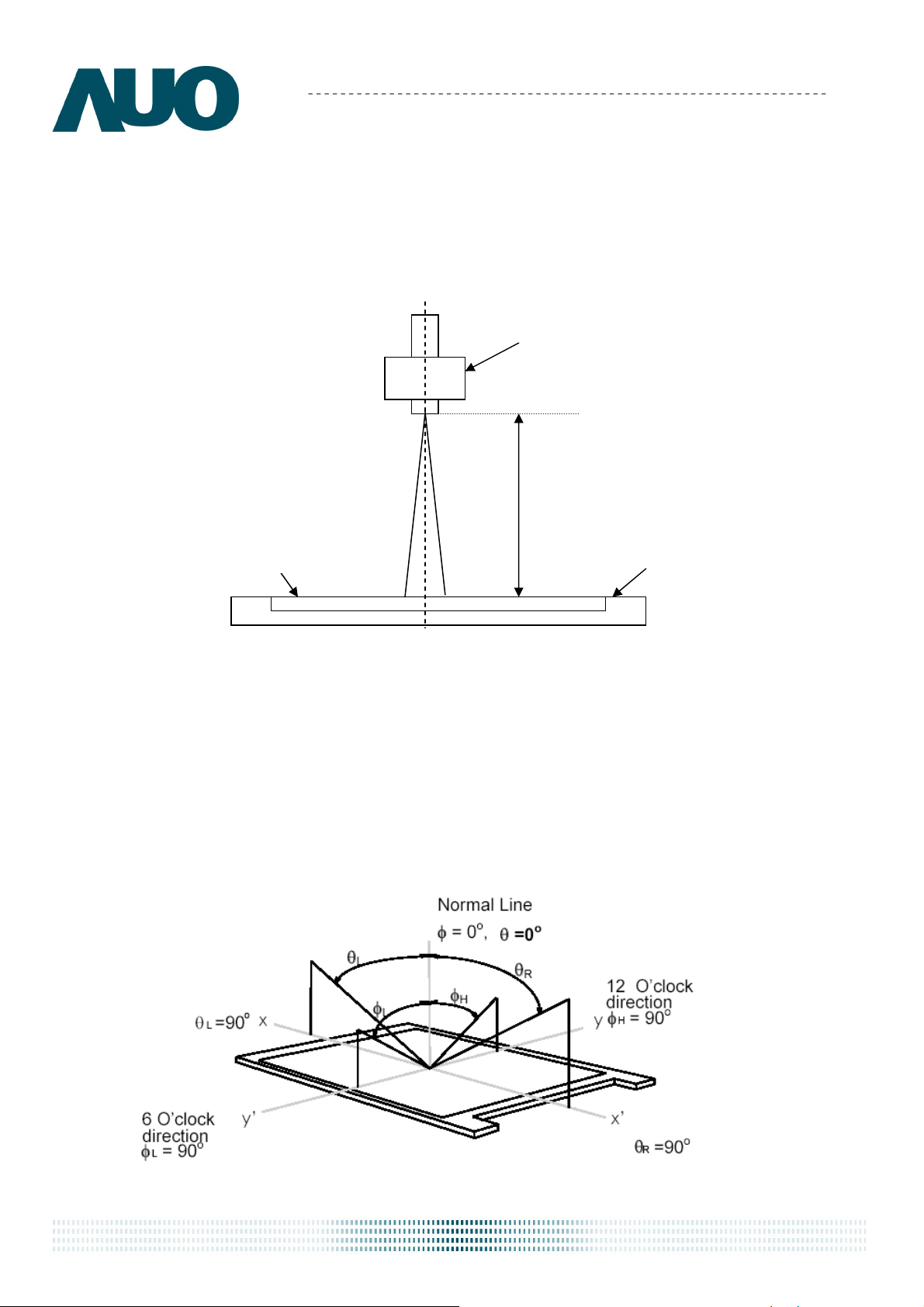
Note 2: Definition of viewing angle measured by ELDIM (EZContrast 88)
Viewing angle is the measurement of contrast ratio ≧10, at the screen center, over a 180°
horizontal and 180° vertical range (off-normal viewing angles). The 180° viewing angle range is
LCD Panel
Measured distance
TFT-LCD Module
broken down as follows; 90° (θ) horizontal left and right and 90° (Φ) vertical, high (up) and low
(down). The measurement direction is typically perpendicular to the display surface with the
screen rotated about its center to develop the desired measurement viewing angle.
document version 1.1 7
Product Specification
90
1 Frame
AU OPTRONICS CORPORATION
M240HW02 V5
Note 3: Contrast ratio is measured by TOPCON SR-3
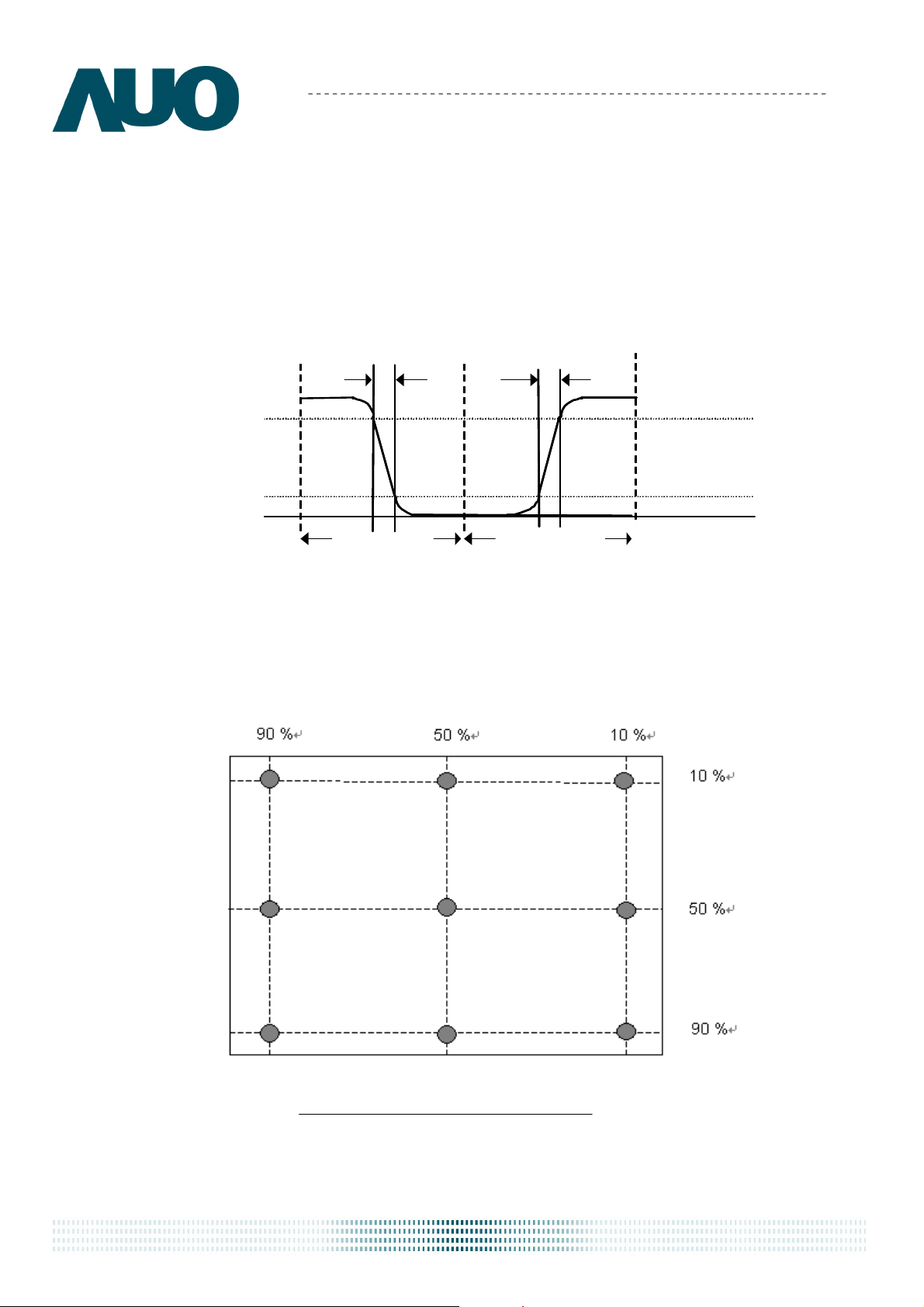
Note 4: Definition of Response time measured by Westar TRD-100A
The output signals of photo detector are measured when the input signals are changed from “Full
Black” to “Full White” (rising time, TrR), and from “Full White” to “Full Black” (falling time, TrF),
respectively. The response time is interval between the 10% and 90% (1 frame at 60 Hz) of
amplitudes.
%
Optical
Optical
response
response
100
100
10
10
%
White
0
0
T
rF
Black
Black
1 Frame
T
rR
White
TrR + TrF = 14 msec (typ.).
Note 5: Color chromaticity and coordinates (CIE) is measured by TOPCON SR-3
Note 6: Central luminance is measured by TOPCON SR-3
Note 7: Luminance uniformity of these 9 points is defined as below and measured by
TOPCON SR-3
Note 8: Crosstalk is defined as below and measured by TOPCON SR-3
Uniformity =
9)-(1 points 9in LuminanceMinimum
9)-(1 Points 9in LuminanceMaximum
document version 1.1 8
Product Specification
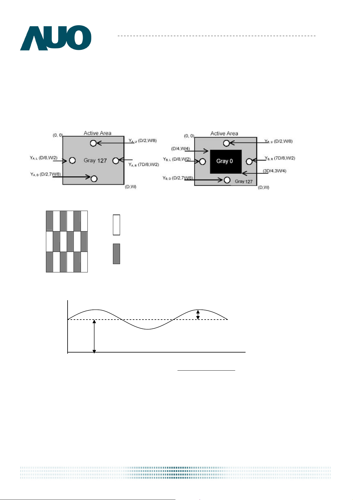
Level
DC
AU OPTRONICS CORPORATION
CT = | YB – YA | / YA × 100 (%)
Where
YA = Luminance of measured location without gray level 0 pattern (cd/m2)
YB = Luminance of measured location with gray level 0 pattern (cd/m2)
M240HW02 V5
Note 9: Test Patern: Subchecker Pattern measured by TOPCON SR-3
G B R G B
R
Gray Level = L127
R G B R G B
R G B R G B
Gray Level = L0
Method: Record dBV & DC value with TRD-100
Amplitude
DC
AC
Time
Hz) 30Level(at AC
log20(dB)Flicker =
document version 1.1 9
Backlight
DC
Connector
LVD
S
Y
-
Driver IC
Connector
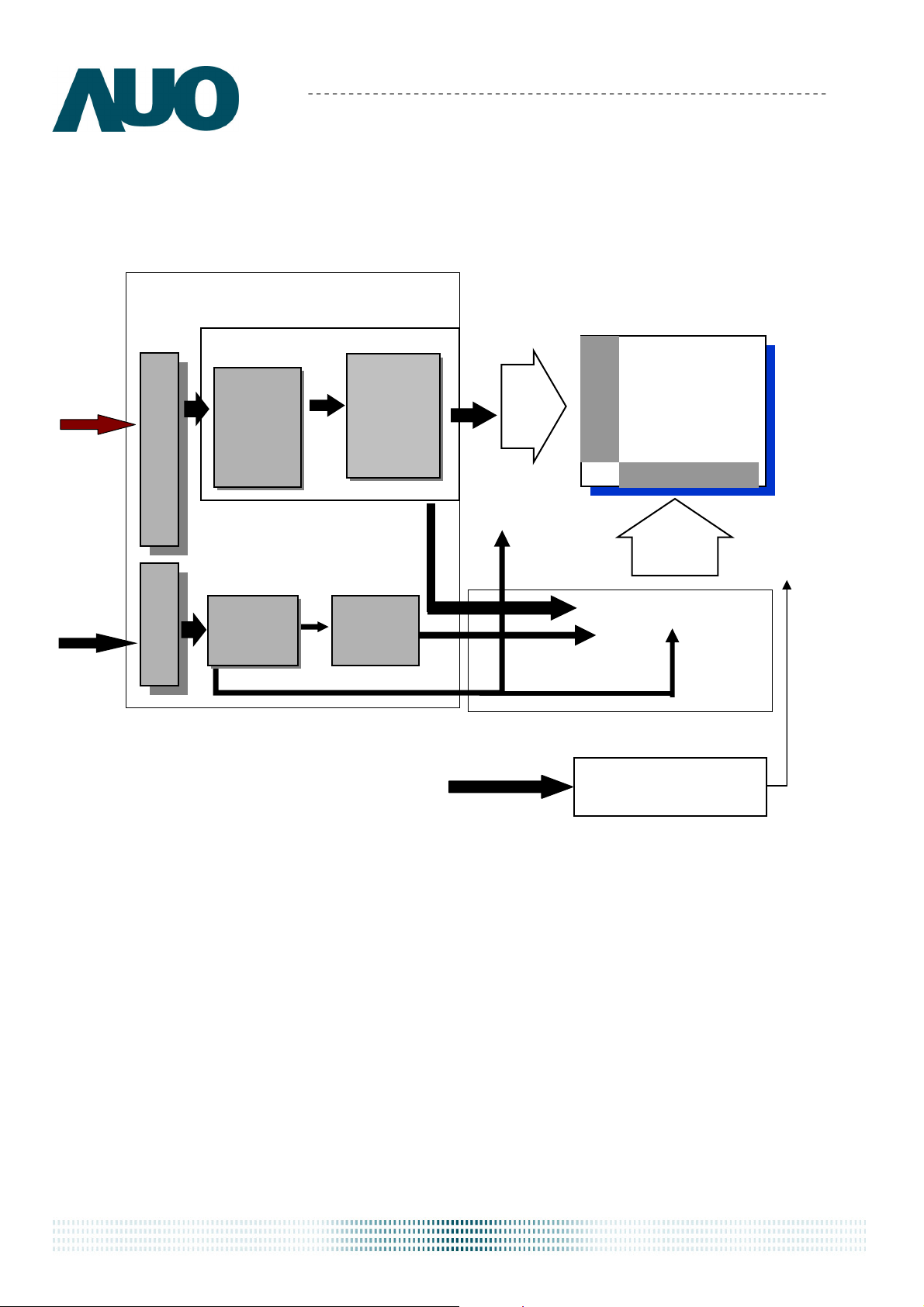
3.0 Functional Block Diagram
Product Specification
AU OPTRONICS CORPORATION
M240HW02 V5
The following diagram shows the functional block of the 24.0 inch Color TFT-LCD Module:
+5V
LVDS
Receiver
DC/DC
Converter
AUO
ASIC
Timing
Controller
miniLVDS
Transmitter
Gamma
Correction
G1
G1080
TFT-LCD
1920(x3) x 1080
Pixels
D1
D5760
LED
I/F PCB Interface:
FI-RE51S-HF
12507WR-H15L
Mating Type:
FI-RE51HL
12507HS-H15L
I/F + X-PCB
LED Driver on system
document version 1.1 10
 Loading...