

Page 1

查询TK5561A-PP供应商
Features
• 65 ms Cycle Time for Crypto Algorithm Programming
• Encryption Time < 10 ms, < 30 ms Optional
• Identification Transponder in Plastic Cube
• Contactless Read/Write Data Transmission
• High-security Crypto Algorithm Optional
• Inductive Coupled Power Supply at 125 kHz
• Basic Component R/W e5561 IDIC
• Built-in Coil and Capacitor for Circuit Antenna
• Starts with Cyclical Data Read Out
• Self-adapting Resonance Frequency (Optional)
• 128-bit User-programmable EEPROM
• Typical < 50 ms to Write and Verify a Block
• Read/Write Protection by Lock Bits
• Options Set by EEPROM:
– Bit Rate (Bit/s): Rf/32, Rf/64
– Modulaton: Manchester, Biphase
â
Read/Write
Crypto
Transponder for
Short Cycle
Application
• Car Immobilizers with Higher Security Level
• High-security Identification Systems
Description
The TK5561A-PP is a complete transponder integrating all important functions for
immobilizer and identification systems. It consists of a plastic cube which accommodates the crypto IDIC e5561A and the antenna realized as tuned LC-circuit. The
TK5561A-PP is a R/W crypto transponder for applications which demand higher security levels than those which standard R/W transponders can fulfil. For this reason, the
TK5561A-PP has an additional encryption algorithm block which enables a base station to authenticate the transponder. Any attempt to fake the base station with a wrong
transponder will be recognized immediately. For authentication, the base station transmits a challenge to the TK5561A-PP. This challenge is encrypted by both the IC and
the base station. Both should possess the same secret key. Only then can the results
be expected to be equal.
For detailed technical information about functions, configurations etc., please refer to
the e5561 data sheet.
Time
TK5561A-PP
Rev. 4682A–RFID–02/03
1
Page 2
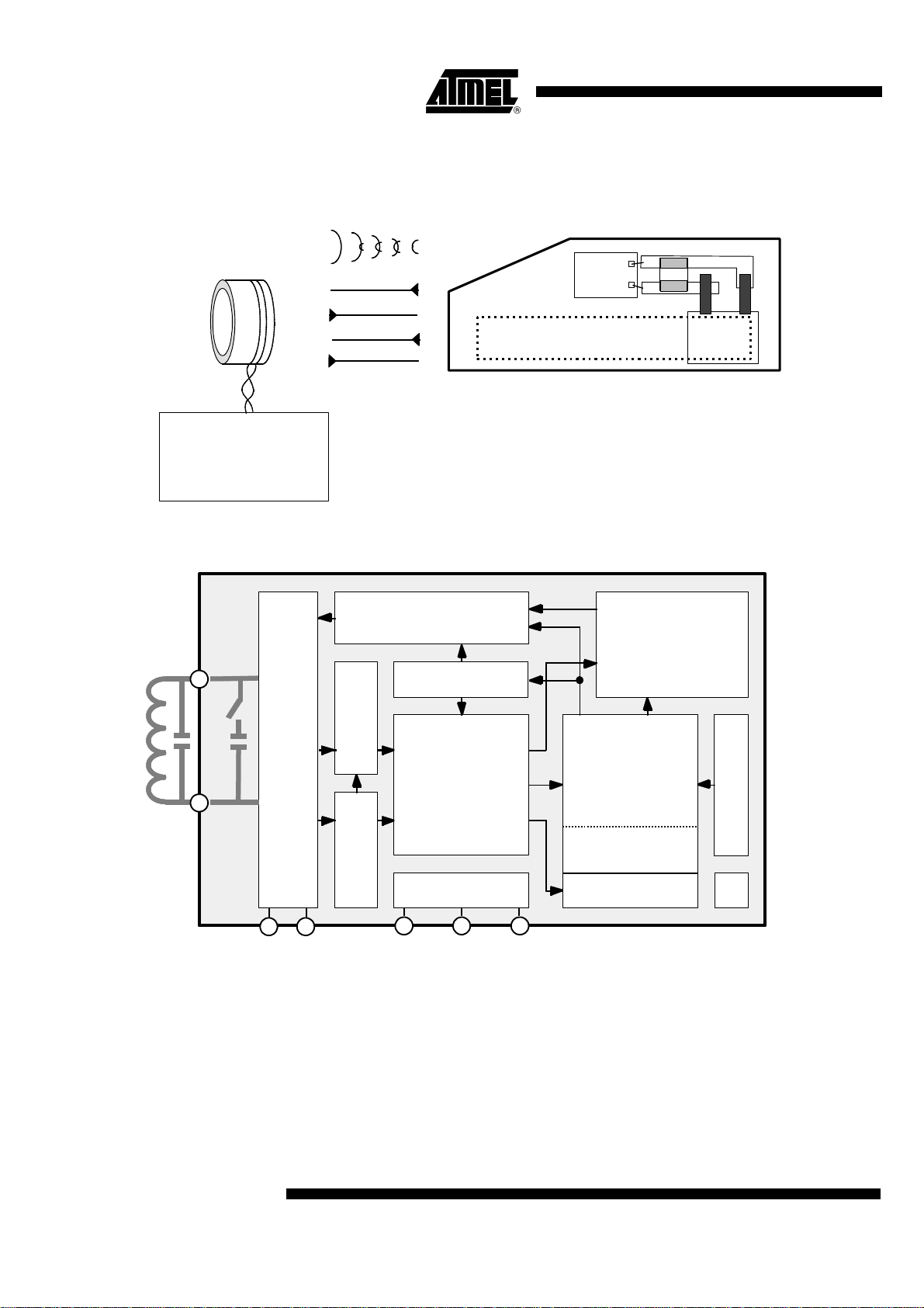
Figure 1. Transponder and Base Station
Base station
U2270B read/write IC
MARC4 series mc
Figure 2. Block Diagram
RF field
Power
ID
Challenge
Response
Transponder TK5561A-PP
(e5561A + coil + C in plastic cube)
C
e5561A
Coil
Coil 1
Coil 2
MODULATOR
CRYPTO CIRCUIT
D
N
E
T
P
A
D
A
T
N
O
R
F
G
O
L
A
N
A
V
V
DD
SS
R
E
E
D
T
I
O
R
C
W
E
D
R
E
O
T
T
A
A
R
R
E
T
I
N
B
E
G
MODE REGISTER
CONTROLLER
crypto control
OP-code detect
EEPROM control
read/write control
TESTLOGIC
Test pads
Memory
(320 bit EEPROM)
crypto key
64 or 128 bit ID code
INPUT REGISTER
POR
R
O
T
A
R
E
N
E
G
V
H
2
TK5561A-PP
4682A–RFID–02/03
Page 3

TK5561A-PP
General The transponder is the mobile part of the closed coupled identification system (see Fig-
ure 1), whereas the read/write base station is based on the U2270B or on discrete
solutions, and the read/write transponder is based on the e5561A IDIC.
The transponder is a plastic-cube device consisting of the following parts:
• The transponder antenna, with a tuned LC-circuit
• Read/write IDIC
Transponder Antenna The antenna consists of a coil and a capacitor for tuning the circuit to the nominal carrier
frequency of 125 kHz. The coil has a ferrite core to improve the read, write and programming operation distances.
(e5561A) with EEPROM
Read/Write Crypto
Identification
The e5561A is a member of the Atmel's contactless IDentification IC (IDIC) family,
which are used in applications where information has to be transmitted without contacts.
The IDIC is connected to a tuned LC circuit for power supply and bidirectional data communication (Read/Write) to a base station.
The on-chip non-volatile memory of the 320-bit EEPROM (10 blocks, 32 bits each) can
be read and written blockwise by a read/write base station, e.g. based on the U2270B.
Up to four blocks consisting of the user programmable ID code, the crypto key and configurations are stored in six blocks. The crypto key and the ID code can be individually
protected against overwriting.
The typical operational frequency of the TK5561A-PP is 125 kHz. Two data bit rates are
programmable: Rf/32 and Rf/64. During the reading operation the incoming RF field is
dampened bit-wise by an on-chip load. This AM-modulation is detected by the field generating base station unit. Data transmission starts after power-up with the transmission
of the ID code and continues as long as the TK5561A-PP is powered.
Writing is carried out by means of Atmel's patented writing method. To transmit data to
the TK5561A-PP the read/write base station has to interrupt the RF field for a short time
to create a field gap. The information is encoded in the number of clock cycles between
two subsequent gaps.
See the e5561A data sheet for detailed information of the IDIC.
4682A–RFID–02/03
3
Page 4

Absolute Maximum Ratings
Parameter Symbol Value Unit
Operating temperature range T
Storage temperature range T
Maximum assembly temperature, t < 5 min T
Magnetic field strength at 125 kHz H
amb
stg
ass
pp
-40 to +85 °C
-40 to +125 °C
170 °C
1000 A/m
Operating Characteristics Transponder
T
= 25°C, f = 125 kHz unless otherwise specified
amb
Parameters Test Conditions Symbol Min. Typ. Max. Unit
Inductance L4.2mH
LC circuit, H
Resonance frequency T
Quality factor Q
Magnetic Field Strength (H)
Max. field strength where
transponder does not modulate
Minimum Field Strength (H)
Read mode
Programming mode
Lowest adapt frequency f
Highest adapt frequency f
Data retention EEPROM T = 25°Ct
Programming cycles EEPROM
Programming time/block RF = 125 kHz t
Maximum field strength H
= 20 A/m
pp
= -40 to +85°C f
amb
No influence to other transponders
H
r
LC
pp not
121 125 129 kHz
5811
in the field
T
= -40°CH
amb
= 25°CH
T
amb
= 85°CH
T
amb
T
= -40°CH
amb
= 25°CH
T
amb
= 85°CH
T
amb
pp -40
pp 25
pp 85
pp -40
pp 25
pp 85
LA
HA
retention
p
pp max
118 121 124.5 kHz
125 128 131.5 kHz
10 Years
100,000
5A/m
24 A/m
18 A/m
15 A/m
30 A/m
35 A/m
40 A/m
16 ms
600 A/m
4
TK5561A-PP
4682A–RFID–02/03
Page 5

Figure 3. Typical Curve for Degree of Modulation
0.5
0.4
0.3
0.2
DV (V)
0.1
0.0
0 20 40 60 80 100 120
Hpp (A/m)
Figure 4. Measurement of the Degree of Modulation
TK5561A-PP
V2V1
V1 V2–
m
------------ ---------=
V1 V2+
4682A–RFID–02/03
5
Page 6

Measurement
Assembly
All parameters are measured in a Helmholtz-arrangement, which generates a homogenous magnetic field (see Figure 5 and Figure 6). A function generator drives the field
generating coils, so the magnetic field can be varied in frequency and field strength.
Figure 5. Testing Application
SENSING COILS ( IN PHASE )
OUTPUT
VOLTAGE
REFERENCE COIL
( IN PHASE )
TK5561A-PP
FIELD GENERATING
COILS ( IN PHASE )
FUNCTION
GENERATOR
SUBTRACTOR
REFERENCE COIL ( IN PHASE )
AMPLIFIER
1:10
Figure 6. Testing Geometry
l = 30 mm
Transponder
22 mm d = 60 mm
REFERENCE COIL
FIELD GENERATING COIL
SENSING COIL
5 mm
SENSING COIL
FIELD GENERATING COIL
REFERENCE COIL
6
TK5561A-PP
4682A–RFID–02/03
Page 7

TK5561A-PP
Writing Data into the
TK5561A-PP
A write sequence of the TK5561A-PP is shown in Figure 7. Writing data into the transponder occurs by interrupting the RF field with short gaps. After the start gap the write
op-code (10) is transmitted. The next 32 bits contain the actual data. The last 4 bits
denote the destination block address. If the correct number of bits have been received,
the actual data is programmed into the specified memory block.
Figure 7. Write Protocol to Program the EEPROM
RF field
Read mode
Writing Data
Decoding
Standard op-code
1
0
Start gap
Write mode
The time elapsing between two detected gaps is used to encode the information. As
soon as a gap is detected, a counter starts counting the number of field clock cycles
until the next gap is detected. Depending on how many field clocks elapse, the data is
regarded as 0 or 1. The required number of field clocks is shown in Figure 8. A valid 0 is
assumed if the number of counted clock periods is between 16 and 31, for a valid 1 it is
48 or 63 respectively. Any other value being detected results in an error and the device
exits write mode and returns to read mode.
32 bit
Address bits (e.g. block 2)
0
1 0 0
> 64 clocks
Figure 8. Write Data Decoding Scheme
11632Field clock cycles
fail 0 fail 1 writing doneWrite data decoder
Actual Device
Behavior
The TK5561A-PP detects a gap if the voltage across the coils decreases below a peakto-peak value of about 800 mV. Until then, the clock pulses are counted. The number
given for a valid 0 or 1 (see Figure 8) refers to the actual clock pulses counted by the
device. However, there are always more clock pulses being counted than were applied
by the base station. The reason for this is the fact that an RF field cannot be switched off
immediately. The coil voltage decreases exponentially. So although the RF field coming
from the base station is switched off, it takes some time until the voltage across the coils
reaches the threshold peak-to-peak value of about 800 mV and the device detects the
gap. Referring to the following diagram Figure 9, this means that the device uses the
times t
cation (e.g., field strength, etc.)
Typical time frames are:
t
= 60 to 140 µs
0
= 300 to 400 µs
t
1
t
gap
Antennas with a high Q-factor require longer times for t
and t1.
48 64
EOT
internal and t1 internal. The exact times for t0 and t1 are dependent on the appli-
0
= 150 to 400 µs
and shorter time values for t
gap
0
4682A–RFID–02/03
7
Page 8

Figure 9. Ideal and Actual Signal Behavior
Coil
voltage
Gap detect
t
gap
t
0
t
1
1 0 1
Ideal behavior
RF level reduces to zero immediately
Coil
voltage
Gap detect
Actual behavior
RF level decreases exponentially
t
t
gap
1
t
0
1 0 1
t
1 internal
t
0 internal
Operating Distance The maximum distance between the base station and the TK5561A-PP depends mainly
on the base station, the coil geometries and the chosen modulation options. Typical distances are 0 to 3 cm. A general maximum distance value cannot be given. A convenient
way is to measure the TK5561A-PP within its environment. Rules for a correct base-station design can be provided upon request (see Antenna Design Guide).
Application
Figure 10. Complete Transponder System with the U2270B Read/Write IC
5 V
5 V
C31
470 kW
47 nF
1.5 nF
4.7 kW
r
e
w
o
P
22 mF
680 pF
1N4148
1.2 nF
1.35 mH
V
V
S
S
EXT
U2270B
RF
MS
CFE
OE
Standby
Output
Gain
Read/Write
circuit
V
Batt
DV
Input
COIL2
R
COIL1
a
t
a
D
DGND GND
110 kW
100 nF
BP00
BP01
BP02
BP03
BP10
V
DD
M44C260
osc IN
osc OUT
Micro-
controller
V
SS
32 kHz
e5561A
Transponde
r
TK5561A-PP
8
TK5561A-PP
f
res
1
LC
2
p
kHz
125
==
4682A–RFID–02/03
Page 9

Mechanical Specification
Figure 11. Mechanical Drawing of Transponder
Dimensions in mm
TK5561A-PP
Ordering Information
Extended Type Number Package Remarks
TK5561A-PP – A = Version of e5561 IDIC
4682A–RFID–02/03
9
Page 10

Atmel Headquarters Atmel Operations
Corporate Headquarters
2325 Orchard Parkway
San Jose, CA 95131
TEL 1(408) 441-0311
FAX 1(408) 487-2600
Europe
Atmel Sarl
Route des Arsenaux 41
Case Postale 80
CH-1705 Fribourg
Switzerland
TEL (41) 26-426-5555
FAX (41) 26-426-5500
Asia
Room 1219
Chinachem Golden Plaza
77 Mody Road Tsimhatsui
East Kowloon
Hong Kong
TEL (852) 2721-9778
FAX (852) 2722-1369
Japan
9F, Tonetsu Shinkawa Bldg.
1-24-8 Shinkawa
Chuo-ku, Tokyo 104-0033
Japan
TEL (81) 3-3523-3551
FAX (81) 3-3523-7581
Memory
2325 Orchard Parkway
San Jose, CA 95131
TEL 1(408) 441-0311
FAX 1(408) 436-4314
Microcontrollers
2325 Orchard Parkway
San Jose, CA 95131
TEL 1(408) 441-0311
FAX 1(408) 436-4314
La Chantrerie
BP 70602
44306 Nantes Cedex 3, France
TEL (33) 2-40-18-18-18
FAX (33) 2-40-18-19-60
ASIC/ASSP/Smart Cards
Zone Industrielle
13106 Rousset Cedex, France
TEL (33) 4-42-53-60-00
FAX (33) 4-42-53-60-01
1150 East Cheyenne Mtn. Blvd.
Colorado Springs, CO 80906
TEL 1(719) 576-3300
FAX 1(719) 540-1759
Scottish Enterprise Technology Park
Maxwell Building
East Kilbride G75 0QR, Scotland
TEL (44) 1355-803-000
FAX (44) 1355-242-743
RF/Automotive
Theresienstrasse 2
Postfach 3535
74025 Heilbronn, Germany
TEL (49) 71-31-67-0
FAX (49) 71-31-67-2340
1150 East Cheyenne Mtn. Blvd.
Colorado Springs, CO 80906
TEL 1(719) 576-3300
FAX 1(719) 540-1759
Biometrics/Imaging/Hi-Rel MPU/
High Speed Converters/RF Datacom
Avenue de Rochepleine
BP 123
38521 Saint-Egreve Cedex, France
TEL (33) 4-76-58-30-00
FAX (33) 4-76-58-34-80
e-mail
literature@atmel.com
Web Site
http://www.atmel.com
© Atmel Corporation 2003.
Atmel Corporation makes no warranty for the use of its products, other than those expressly contained in the Company’s standard warranty
which is detailed in Atmel’s Terms and Conditions located on the Company’s web site. The Company assumes no responsibility for any errors
which may appear in this document, reserves the right to change devices or specifications detailed herein at any time without notice, and does
not make any commitment to update the information contained herein. No licenses to patents or other intellectual property of Atmel are granted
by the Company in connection with the sale of Atmel products, expressly or by implication. Atmel’s products are not authorized for use as critical
components in life support devices or systems.
Atmel® is the registered trademark of Atmel.
Ò
stands for IDentification Integrated Circuit and is a registered trademark of Atmel Germany GmbH.
IDIC
Other terms and product names may be the trademarks of others.
Printed on recycled paper.
4682A–RFID–02/03
xM
 Loading...