


Features
• Core
• Pin-to-pin compatible with AT91SAM7S legacy products (48- and 64-pin versions) and
ATSAM3S (48-, 64- and 100-pin version)
• Memories
• System
• Low Power Modes
• Peripherals
• I/O
• Packages
®
– ARM
–Thumb
– 24-bit SysTick Counter
– Nested Vector Interrupt Controller
– From 64 to 256 Kbytes embedded Flash, 128-bit wide access, memory accelerator,
– From 8 to 24 Kbytes embedded SRAM
– 16 Kbytes ROM with embedded bootloader routines (UART) and IAP routines
– Embedded voltage regulator for single supply operation
– Power-on-Reset (POR), Brown-out Detector (BOD) and Watchdog for safe
– Quartz or ceramic resonator oscillators: 3 to 20 MHz main power with Failure
– High precision 8/12 MHz factory trimmed internal RC oscillator with 4 MHz default
– Slow Clock Internal RC oscillator as permanent low-power mode device clock
– One PLL up to 130 MHz for device clock
– Up to 10 peripheral DMA (PDC) channels
– Sleep and Backup modes, down to 3 µA in Backup mode
– Ultra low power RTC
– Up to 2 USARTs with ISO7816, IrDA
– Two 2-wire UARTs
– 2 Two Wire Interface (I2C compatible), 1 SPI
– Up to 6 Three-Channel 16-bit Timer/Counter with capture, waveform, compare and
– 4-channel 16-bit PWM
– 32-bit Real-time Timer and RTC with calendar and alarm features
– Up to 16 channels, 384 KSPS 10-bit ADC
– One 500 KSPS 10-bit DAC
– Up to 79 I/O lines with external interrupt capability (edge or level sensitivity),
– Three 32-bit Parallel Input/Output Controllers
– 100-lead LQFP, 14 x 14 mm, pitch 0.5 mm / 100-ball LFBGA, 9 x 9 mm, pitch 0.8 mm
– 64-lead LQFP, 12 x 12 mm, pitch 0.5 mm / 64-pad QFN 9x9 mm, pitch 0.45 mm
– 48-lead LQFP, 9 x 9 mm, pitch 0.5 mm / 48-pad QFN 7x7 mm, pitch 0.45 mm
Cortex®-M3 revision 2.0 running at up to 48 MHz
®
-2 instruction
single plane
operation
Detection and optional low power 32.768 kHz for RTC or device clock
frequency for device startup. In-application trimming access for frequency
adjustment
®
, RS-485 and SPI mode
PWM mode. Quadrature Decoder Logic and 2-bit Gray Up/Down Counter for
Stepper Motor
debouncing, glitch filtering and on-die Series Resistor Termination
AT91SAM
ARM-based
Flash MCU
SAM3N Series
Summary
NOTE: This is a summary document.
The complete document is available
under NDA. For more information,
please contact your local Atmel sales
office.
11011AS–ATARM–04-Oct-10

1. SAM3N Description
Atmel's SAM3N series is a member of a family of Flash microcontrollers based on the high performance 32-bit ARM Cortex-M3 RISC processor. It operates at a maximum speed of 48 MHz
and features up to 256 Kbytes of Flash and up to 24 Kbytes of SRAM. The peripheral set
includes 2x USARTs, 2x UARTs, 2x TWIs, 3x SPI, as well as 1 PWM timer, 6x general purpose
16-bit timers, an RTC, a 10-bit ADC and a 10-bit DAC.
The SAM3N series is ready for capacitive touch thanks to the QTouch library, offering an easy
way to implement buttons, wheels and sliders.
The SAM3N device is an entry-level general purpose microcontroller. That makes the SAM3N
the ideal starting point to move from 8- /16-bit to 32-bit microcontrollers.
It operates from 1.62V to 3.6V and is available in 48-pin, 64-pin and 100-pin QFP, 48-pin and
64-pin QFN, and 100-pin BGA packages.
The SAM3N series is the ideal migration path from the SAM3S for applications that require a
reduced BOM cost. The SAM3N series is pin-to-pin compatible with the SAM3S series. Its
aggressive price point and high level of integration pushes its scope of use far into cost-sensitive, high-volume applications.
1.1 Configuration Summary
The SAM3N4/2/1 differ in memory size, package and features list. Table 1-1 summarizes the
configurations of the 9 devices.
Table 1-1. Configuration Summary
Device Flash SRAM Package
ATSAM3N4A 256 Kbytes 24 Kbytes
ATSAM3N4B 256 Kbytes 24 Kbytes
ATSAM3N4C 256 Kbytes 24 Kbytes
ATSAM3N2A 128 Kbytes 16 Kbytes
ATSAM3N2B 128 Kbytes 16 Kbytes
ATSAM3N2C 128 Kbytes 16 Kbytes
ATSAM3N1A 64 Kbytes 8 Kbytes
ATSAM3N1B 64 Kbytes 8 Kbytes
ATSAM3N1C 64 Kbytes 8 Kbytes
LQFP48
QFN48
LQFP64
QFN64
LQFP100
BGA100
LQFP48
QFN48
LQFP64
QFN64
LQFP100
BGA100
LQFP48
QFN48
LQFP64
QFN64
LQFP100
BGA100
Number
of PIOs ADC Timer
34 8 channels 6
47 10 channels 6
79 16 channels 6 10 2 1
34 8 channels 6
47 10 channels 6(
79 16 channels 6 10 2 1
34 8 channels 6
47 10 channels 6
79 16 channels 6 10 2 1
(1)
(2)
(1)
(2)
(1)
(2)
PDC
Channels USART DAC
81_
10 2 1
81 _
10 2 1
81 _
10 2 1
Notes: 1. Only two TC channels are accessible through the PIO.
2. Only three TC channels are accessible through the PIO.
2
SAM3N Summary
11011AS–ATARM–04-Oct-10

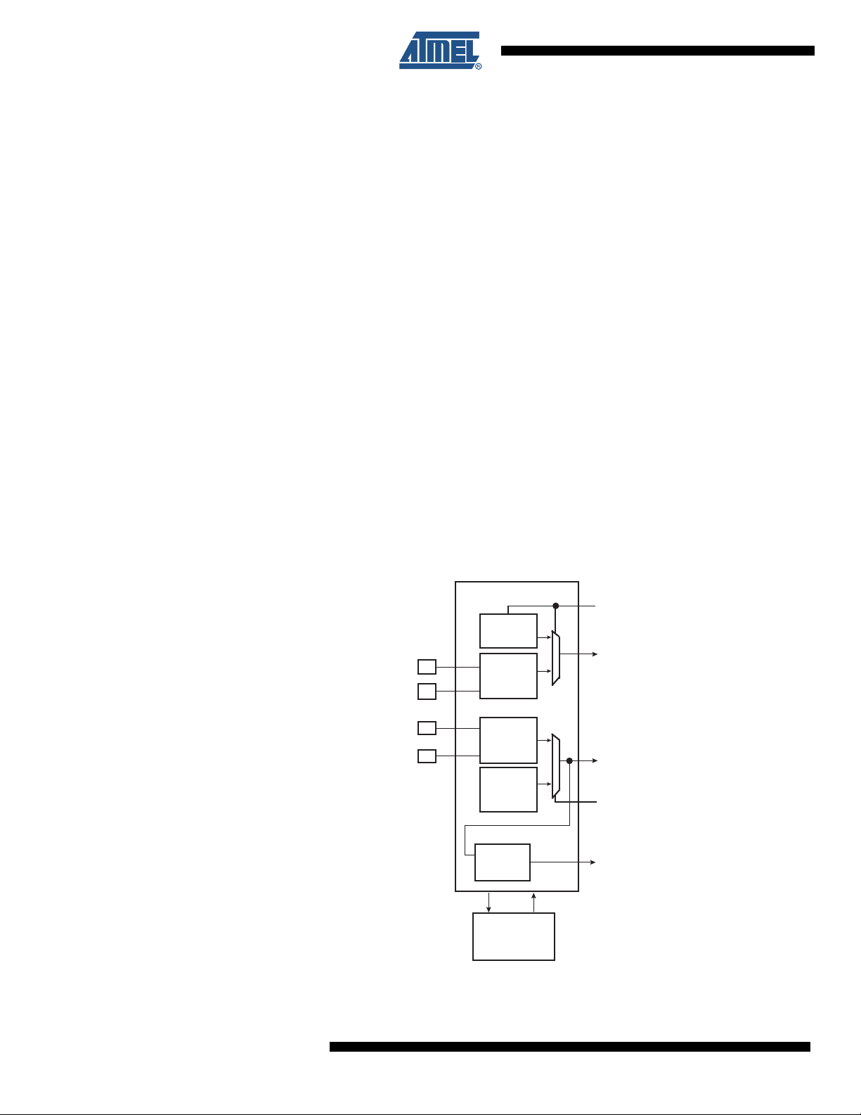
2. SAM3N Block Diagram
Figure 2-1. SAM3N 100-pin version Block Diagram
SAM3N Summary
PCK0-PCK2
XOUT
XIN32
XOUT32
ERASE
VDDIO
NRST
VDDCORE
URXD0
UTXD0
URXD1
UTXD1
RXD0
TXD0
SCK0
RTS0
CTS0
RXD1
TXD1
SCK1
RTS1
CTS1
PWM[0:3]
ADTRG
AD[0..15]
ADVREF
DAC0
DATRG
TST
XIN
System Controller
PMC
OSC
3-20 MHz
WDT
RC OSC
12/8/4 MHz
SUPC
OSC 32k
RC 32k
PLL
RTT
RTC
POR
RSTC
PIOA PIOB
PIOC
SM
10-bit ADC
10-bit DAC
TDI
TCK/SWCLK
TDO/TRACESWO
TMS/SWDIO
JTAG & Serial Wire
In-Circuit Emulator
Cortex-M3 Processor
Fmax 48 MHz
I/D
UART0
PDC
UART1
USART0
PDC
USART1
PWM
PDC
PDC
JTAGSEL
24-bit
SysTick Counter
N
V
I
C
FLASH
256 KBytes
128 KBytes
64 KBytes
S
3- layer AHB Bus Matrix Fmax 48 MHz
Peripheral
Bridge
VDDINVDDOUT
Voltage
Regulator
SRAM
24 KBytes
16 KBytes
8 KBytes
Timer Counter A
TC[0..2]
Timer Counter B
TC[3..5]
PDC
SPI
PDC
TWI0
TWI1
ROM
16 KBytes
TCLK[0:2]
TIOA[0:2]
TIOB[0:2]
TCLK[3:5]
TIOA[3:5]
TIOB[3:5]
NPCS0
NPCS1
NPCS2
NPCS3
MISO
MOS
SPCK
TWCK0
TWD0
TWCK1
TWD1
11011AS–ATARM–04-Oct-10
3

Figure 2-2. SAM3N 64-pin version Block Diagram
TC[3..5]
AD[0..9]
3- layer AHB Bus Matrix Fmax 48 MHz
TST
PCK0-PCK2
System Controller
XIN
NRST
PMC
XOUT
OSC 32k
XIN32
XOUT32
SUPC
RSTC
OSC
3-20 MHz
PIOA PIOB
POR
RTC
RTT
RC 32k
RC OSC
12/8/4 MHz
ERASE
TDI
TDO/TRACESWO
TMS/SWDIO
TCK/SWCLK
JTAGSEL
I/D
S
VDDINVDDOUT
TC[0..2]
TCLK[0:2]
TWCK0
TWD0
TWCK1
TWD1
NPCS0
NPCS1
NPCS2
NPCS3
MISO
MOS
SPCK
TIOA[0:2]
TIOB[0:2]
PDC
PDC
PDC
PDC
PDC
PWM
In-Circuit Emulator
PDC
JTAG & Serial Wire
PWM[0:3]
ADTRG
ADVREF
DAC0
DATRG
10-bit ADC
10-bit DAC
SM
VDDIO
PLL
RXD0
TXD0
SCK0
RTS0
CTS0
RXD1
TXD1
SCK1
RTS1
CTS1
USART0
UART1
UART0
USART1
Cortex-M3 Processor
Fmax 48 MHz
24-bit
SysTick Counter
ROM
16 KBytes
SRAM
24 KBytes
16 KBytes
8 KBytes
FLASH
256 KBytes
128 KBytes
64 KBytes
VDDCORE
WDT
Peripheral
Bridge
URXD0
UTXD0
URXD1
UTXD1
Timer Counter A
Timer Counter B
SPI
TWI0
TWI1
N
V
I
C
Voltage
Regulator
3-layer AHB Bus Matrix Fmax 48 MHz
4
SAM3N Summary
11011AS–ATARM–04-Oct-10

Figure 2-3. SAM3N 48-pin version Block Diagramz
SAM3N Summary
PCK0-PCK2
XOUT
XIN32
XOUT32
ERASE
VDDIO
NRST
VDDCORE
URXD0
UTXD0
URXD1
UTXD1
TST
XIN
System Controller
PMC
3-20 MHz
WDT
RC OSC
12/8/4 MHz
SUPC
OSC 32k
RC 32k
RTC
POR
RSTC
PIOA PIOB
OSC
SM
PLL
RTT
TDI
TCK/SWCLK
TDO/TRACESWO
TMS/SWDIO
JTAG & Serial Wire
In-Circuit Emulator
Cortex-M3 Processor
Fmax 48 MHz
I/D
UART0
PDC
UART1
JTAGSEL
24-bit
SysTick Counter
N
V
I
C
FLASH
256 KBytes
128 KBytes
64 KBytes
S
3-layer AHB Bus Matrix Fmax 48 MHz
3- layer AHB Bus Matrix Fmax 48 MHz
Peripheral
Bridge
N
VDDOUT
VDDI
Voltage
Regulator
SRAM
24 KBytes
16 KBytes
8 KBytes
Timer Counter A
TC[0..2]
ROM
16 KBytes
TCLK[0:2]
TIOA[0:2]
TIOB[0:2]
RXD0
TXD0
SCK0
RTS0
CTS0
PWM[0:3]
ADTRG
AD[0..7]
ADVREF
USART0
PWM
10-bit ADC
PDC
PDC
Timer Counter B
TC[3..5]
PDC
SPI
PDC
TWI0
TWI1
NPCS0
NPCS1
NPCS2
NPCS3
MISO
MOS
SPCK
TWCK0
TWD0
TWCK1
TWD1
11011AS–ATARM–04-Oct-10
5

3. Signal Description
Table 3-1 gives details on the signal name classified by peripheral.
Table 3-1. Signal Description List
Active
Signal Name Function Type
Power Supplies
VDDIO Peripherals I/O Lines Power Supply Power 1.62V to 3.6V
VDDIN
VDDOUT Voltage Regulator Output Power 1.8V Output
VDDPLL Oscillator and PLL Power Supply Power 1.65 V to 1.95V
VDDCORE
GND Ground Ground
XIN Main Oscillator Input Input
XOUT Main Oscillator Output Output
XIN32 Slow Clock Oscillator Input Input
XOUT32 Slow Clock Oscillator Output Output
PCK0 - PCK2 Programmable Clock Output Output
Voltage Regulator, ADC and DAC Power
Supply
Power the core, the embedded memories
and the peripherals
Clocks, Oscillators and PLLs
Power 1.8V to 3.6V
Power
Level
Voltage
Reference Comments
1.65V to 1.95V
Connected externally
to VDDOUT
Reset State:
- PIO Input
- Internal Pull-up
disabled
VDDIO
- Schmitt Trigger
enabled
Reset State:
- PIO Input
- Internal Pull-up
enabled
- Schmitt Trigger
enabled
(1)
(1)
(3)
ICE and JTAG
TCK/SWCLK Test Clock/Serial Wire Clock Input
TDI Test Data In Input
TDO/TRACESWO
TMS/SWDIO
JTAGSEL JTAG Selection Input High
6
SAM3N Summary
Test Data Out/Trace Asynchronous Data
Out
Test Mode Select /Serial Wire
Input/Output
Output
Input / I/O
VDDIO
Reset State:
- SWJ-DP Mode
- Internal pull-up
disabled
- Schmitt Trigger
enabled
Permanent Internal
pull-down
11011AS–ATARM–04-Oct-10
(1)

Table 3-1. Signal Description List (Continued)
SAM3N Summary
Active
Signal Name Function Type
Flash Memory
ERASE
NRST Microcontroller Reset I/O Low VDDIO
TST Test Mode Select Input VDDIO
URXDx UART Receive Data Input
UTXDx UART Transmit Data Output
PA0 - PA31 Parallel IO Controller A I/O
PB0 - PB14 Parallel IO Controller B I/O
PC0 - PC31 Parallel IO Controller C I/O
SCKx USARTx Serial Clock I/O
Flash and NVM Configuration Bits Erase
Command
Reset/Test
Universal Asynchronous Receiver Transceiver - UARTx
PIO Controller - PIOA - PIOB - PIOC
Universal Synchronous Asynchronous Receiver Transmitter USARTx
Input High VDDIO
Level
Voltage
Reference Comments
VDDIO
Reset State:
- Erase Input
- Internal pull-down
enabled
- Schmitt Trigger
enabled
Permanent Internal
pull-up
Permanent Internal
pull-down
Reset State:
- PIO or System
IOs
- Internal pull-up
enabled
- Schmitt Trigger
enabled
(1)
(2)
(1)
TXDx USARTx Transmit Data I/O
RXDx USARTx Receive Data Input
RTSx USARTx Request To Send Output
CTSx USARTx Clear To Send Input
Timer/Counter - TC
TCLKx TC Channel x External Clock Input Input
TIOAx TC Channel x I/O Line A I/O
TIOBx TC Channel x I/O Line B I/O
Pulse Width Modulation Controller- PWMC
PWMx PWM Waveform Output for channel x Output
11011AS–ATARM–04-Oct-10
7

Table 3-1. Signal Description List (Continued)
Active
Signal Name Function Type
Serial Peripheral Interface - SPI
MISO Master In Slave Out I/O
MOSI Master Out Slave In I/O
SPCK SPI Serial Clock I/O
SPI_NPCS0 SPI Peripheral Chip Select 0 I/O Low
SPI_NPCS1 SPI_NPCS3
TWDx TWIx Two-wire Serial Data I/O
TWCKx TWIx Two-wire Serial Clock I/O
ADVREF ADC and DAC Reference Analog
AD0 - AD15 Analog Inputs Analog
ADTRG ADC Trigger Input VDDIO
DAC0 DACC channel analog output Analog
DATRG DACC Trigger Input VDDIO
SPI Peripheral Chip Select Output Low
Two-Wire Interface- TWIx
Analog
10-bit Analog-to-Digital Converter - ADC
Digital-to-Analog Converter Controller- DACC
Level
Voltage
Reference Comments
Fast Flash Programming Interface
PGMEN0-PGMEN2 Programming Enabling Input
PGMM0-PGMM3 Programming Mode Input
PGMD0-PGMD15 Programming Data I/O
PGMRDY Programming Ready Output High
PGMNVALID Data Direction Output Low
PGMNOE Programming Read Input Low
PGMCK Programming Clock Input
PGMNCMD Programming Command Input Low
Notes: 1. Schmitt Triggers can be disabled through PIO registers.
2. Some PIO lines are shared with System IOs.
3. See Section 5.3 “Typical Powering Schematics” for restriction on voltage range of Analog Cells.
VDDIO
8
SAM3N Summary
11011AS–ATARM–04-Oct-10

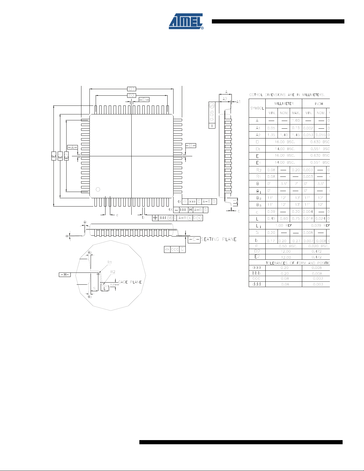
4. Package and Pinout
125
26
50
5175
76
100
SAM3N4/2/1 series is pin-to-pin compatible with SAM3S products. Furthermore SAM3N4/2/1
devices have new functionalities referenced in italic inTable 4-1, Table 4-3 and Table 4-4.
4.1 SAM3N4/2/1C Package and Pinout
4.1.1 100-lead LQFP Package Outline
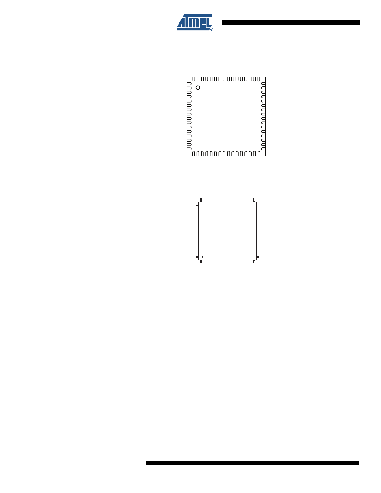
Figure 4-1. Orientation of the 100-lead LQFP Package
SAM3N Summary
4.1.2 100-ball LFBGA Package Outline
The 100-Ball LFBGA package has a 0.8 mm ball pitch and respects Green Standards. Its dimensions are 9 x 9 x 1.1 mm.
Figure 4-2. Orientation of the 100-ball LFBGA Package
TOP VIEW
10
9
8
7
6
5
4
3
2
1
ABCDEFGHJK
BALL A1
9
11011AS–ATARM–04-Oct-10

4.1.3 100-Lead LQFP Pinout
Table 4-1. 100-lead LQFP SAM3N4/2/1C Pinout
1 ADVREF 26 GND 51 TDI/PB4 76 TDO/TRACESWO/PB5
2 GND 27 VDDIO 52 PA6/PGMNOE 77 JTAGSEL
3 PB0/AD4 28 PA16/PGMD4 53 PA5/PGMRDY 78 PC18
4 PC29/AD13 29 PC7 54 PC28 79 TMS/SWDIO/PB6
5 PB1/AD5 30 PA15/PGMD3 55 PA4/PGMNCMD 80 PC19
6 PC30/AD14 31 PA14/PGMD2 56 VDDCORE 81 PA31
7 PB2/AD6 32 PC6 57 PA27 82 PC20
8 PC31/AD15 33 PA13/PGMD1 58 PC8 83 TCK/SWCLK/PB7
9 PB3/AD7 34 PA24 59 PA28 84 PC21
10 VDDIN 35 PC5 60 NRST 85 VDDCORE
11 VDDOUT 36 VDDCORE 61 TST 86 PC22
12 PA17/PGMD5/AD0 37 PC4 62 PC9 87 ERASE/PB12
13 PC26 38 PA25 63 PA29 88 PB10
14 PA18/PGMD6/AD1 39 PA26 64 PA30 89 PB11
15 PA21/AD8 40 PC3 65 PC10 90 PC23
16 VDDCORE 41 PA12/PGMD0 66 PA3 91 VDDIO
17 PC27 42 PA11/PGMM3 67 PA2/PGMEN2 92 PC24
18 PA19/PGMD7/AD2 43 PC2 68 PC11 93 PB13/DAC0
19 PC15/AD11 44 PA10/PGMM2 69 VDDIO 94 PC25
20 PA22/AD9 45 GND 70 GND 95 GND
21 PC13/AD10 46 PA9/PGMM1 71 PC14 96 PB8/XOUT
22 PA23 47 PC1 72 PA1/PGMEN1 97 PB9/PGMCK/XIN
23 PC12/AD12 48
24 PA20/AD3 49
25 PC0 50 VDDIO 75 PC17 100 VDDPLL
PA8/XOUT32/
PGMM0
PA7/XIN32/
PGMNVALID
73 PC16 98 VDDIO
74 PA0/PGMEN0 99 PB14
10
SAM3N Summary
11011AS–ATARM–04-Oct-10

4.1.4 100-ball LFBGA Pinout
Table 4-2. 100-ball LFBGA SAM3N4/2/1C Pinout
SAM3N Summary
A1 PB1/AD5 C6 TCK/SWCLK/PB7 F1
A2 PC29 C7 PC16 F2 PC26 H7 PA11/PGMM3
A3 VDDIO C8 PA1/PGMEN1 F3 VDDOUT H8 PC1
A4 PB9/PGMCK/XIN C9 PC17 F4 GND H9 PA6/PGMNOE
A5 PB8/XOUT C10 PA0/PGMEN0 F5 VDDIO H10 TDI/PB4
A6 PB13/DAC0 D1 PB3/AD7 F6 PA27 J1 PC15/AD11
A7 DDP/PB11 D2 PB0/AD4 F7 PC8 J2 PC0
A8 DDM/PB10 D3 PC24 F8 PA28 J3 PA16/PGMD4
A9 TMS/SWDIO/PB6 D4 PC22 F9 TST J4 PC6
A10 JTAGSEL D5 GND F10 PC9 J5 PA24
B1 PC30 D6 GND G1 PA21/AD8 J6 PA25
B2 ADVREF D7 VDDCORE G2 PC27 J7 PA10/PGMM2
B3 GNDANA D8 PA2/PGMEN2 G3 PA15/PGMD3 J8 GND
B4 PB14/DAC1 D9 PC11 G4 VDDCORE J9 VDDCORE
B5 PC21 D10 PC14 G5 VDDCORE J10 VDDIO
B6 PC20 E1
PA17/PGMD5/
AD0
G 6 PA 2 6 K 1 PA 22 / AD 9
PA 1 8/ P G MD 6 /
AD1
H6 PC4
B7 PA31 E2 PC31 G7 PA12/PGMD0 K2 PC13/AD10
B8 PC19 E3 VDDIN G8 PC28 K3 PC12/AD12
B9 PC18 E4 GND G9 PA4/PGMNCMD K4 PA20/AD3
B10
TDO/TRACESWO/
PB5
C1 PB2/AD6 E6 NRST H1
C2 VDDPLL E7 PA29/AD13 H2 PA23 K7 PC2
C3 PC25 E8 PA30/AD14 H3 PC7 K8 PA9/PGMM1
C4 PC23 E9 PC10 H4 PA14/PGMD2 K9
C5 ERASE/PB12 E10 PA3 H5 PA13/PGMD1 K10
E5 GND G10 PA5/PGMRDY K5 PC5
PA 1 9/ P G MD 7 /
AD2
K6 PC3
PA8/XOUT32/
PGMM0
PA7/XIN32/
PGMNVALID
11011AS–ATARM–04-Oct-10
11
4.2 SAM3N4/2/1B Package and Pinout
Figure 4-3. Orientation of the 64-pad QFN Package
4964
1
48
16
17
TOP VIEW
Figure 4-4. Orientation of the 64-lead LQFP Package
48
49
64
1
33
32
33
32
17
16
12
SAM3N Summary
11011AS–ATARM–04-Oct-10
SAM3N Summary
4.2.1 64-Lead LQFP and QFN Pinout
64-pin version SAM3N devices are pin-to-pin compatible with SAM3S products. Furthermore,
SAM3N products have new functionalities shown in italic in Table 4-3.
Table 4-3. 64-pin SAM3N4/2/1B Pinout
1 ADVREF 17 GND 33 TDI/PB4 49 TDO/TRACESWO/PB5
2 GND 18 VDDIO 34 PA6/PGMNOE 50 JTAGSEL
3 PB0/AD4 19 PA16/PGMD4 35 PA5/PGMRDY 51 TMS/SWDIO/PB6
4 PB1AD5 20 PA15/PGMD3 36 PA4/PGMNCMD 52 PA31
5 PB2/AD6 21 PA14/PGMD2 37 PA27/PGMD15 53 TCK/SWCLK/PB7
6 PB3/AD7 22 PA13/PGMD1 38 PA28 54 VDDCORE
7 VDDIN 23 PA24/PGMD12 39 NRST 55 ERASE/PB12
8 VDDOUT 24 VDDCORE 40 TST 56 PB10
9 PA17/PGMD5/AD0 25 PA25/PGMD13 41 PA29 57 PB11
10 PA18/PGMD6/AD1 26 PA26/PGMD14 42 PA30 58 VDDIO
11 PA21/PGMD9/AD8 27 PA12/PGMD0 43 PA3 59 PB13/DAC0
12 VDDCORE 28 PA11/PGMM3 44 PA2/PGMEN2 60 GND
13 PA19/PGMD7/AD2 29 PA10/PGMM2 45 VDDIO 61 XOUT/PB8
14 PA22/PGMD10/AD9 30 PA9/PGMM1 46 GND 62 XIN/PGMCK/PB9
15 PA23/PGMD11 31
16 PA20/PGMD8/AD3 32
Note: The bottom pad of the QFN package must be connected to ground.
PA8/XOUT32/PGMM
0
PA7/XIN32/XOUT32/
PGMNVALID
47 PA1/PGMEN1 63 PB14
48 PA0/PGMEN0 64 VDDPLL
11011AS–ATARM–04-Oct-10
13

4.3 SAM3N4/2/1A Package and Pinout
25
37
36
24
13
12
1
48
Figure 4-5. Orientation of the 48-pad QFN Package
3748
1
12
13 24
TOP VIEW
Figure 4-6. Orientation of the 48-lead LQFP Package
36
25
14
SAM3N Summary
11011AS–ATARM–04-Oct-10

4.3.1 48-Lead LQFP and QFN Pinout
Table 4-4. 48-pin SAM3N4/2/1A Pinout
SAM3N Summary
1 ADVREF 13 VDDIO 25 TDI/PB4 37
2 GND 14 PA16/PGMD4 26 PA6/PGMNOE 38 JTAGSEL
3 PB0/AD4 15 PA15/PGMD3 27 PA5/PGMRDY 39 TMS/SWDIO/PB6
4 PB1/AD5 16 PA14/PGMD2 28 PA4/PGMNCMD 40 TCK/SWCLK/PB7
5 PB2/AD6 17 PA13/PGMD1 29 NRST 41 VDDCORE
6 PB3/AD7 18 VDDCORE 30 TST 42 ERASE/PB12
7 VDDIN 19 PA12/PGMD0 31 PA3 43 PB10
8 VDDOUT 20 PA11/PGMM3 32 PA2/PGMEN2 44 PB11
9 PA17/PGMD5/AD0 21 PA10/PGMM2 33 VDDIO 45 XOUT/PB8
10 PA18/PGMD6/AD1 22 PA9/PGMM1 34 GND 46 XIN/P/PB9/GMCK
11 PA19/PGMD7/AD2 23
12 PA20/AD3 24
Note: The bottom pad of the QFN package must be connected to ground.
PA8/XOUT32/PG
MM0
PA7/XIN32/PGMN
VALID
35 PA1/PGMEN1 47 VDDIO
36 PA0/PGMEN0 48 VDDPLL
TDO/TRACESWO/
PB5
11011AS–ATARM–04-Oct-10
15

5. Power Considerations
5.1 Power Supplies
The SAM3N product has several types of power supply pins:
• VDDCORE pins: Power the core, including the processor, the embedded memories and the
peripherals. Voltage ranges from 1.62V and 1.95V.
• VDDIO pins: Power the Peripherals I/O lines, Backup part, 32 kHz crystal oscillator and
oscillator pads. Voltage ranges from 1.62V and 3.6V
• VDDIN pin: Voltage Regulator, ADC and DAC Power Supply. Voltage ranges from 1.8V to
3.6V for the Voltage Regulator
• VDDPLL pin: Powers the PLL, the Fast RC and the 3 to 20 MHz oscillators. Voltage ranges
from 1.62V and 1.95V.
5.2 Voltage Regulator
The SAM3N embeds a voltage regulator that is managed by the Supply Controller.
This internal regulator is intended to supply the internal core of SAM3N. It features two different
operating modes:
• In Normal mode, the voltage regulator consumes less than 700 µA static current and draws
60 mA of output current. Internal adaptive biasing adjusts the regulator quiescent current
depending on the required load current. In Wait Mode quiescent current is only 7 µA.
• In Backup mode, the voltage regulator consumes less than 1 µA while its output (VDDOUT)
is driven internally to GND. The default output voltage is 1.80V and the start-up time to reach
Normal mode is less than100 µs.
For adequate input and output power supply decoupling/bypassing, refer to the Voltage Regulator section in the Electrical Characteristics section of the datasheet.
5.3 Typical Powering Schematics
The SAM3N supports a 1.62V-3.6V single supply mode. The internal regulator input connected
to the source and its output feeds VDDCORE. Figure 5-1 shows the power schematics.
As VDDIN powers the voltage regulator and the ADC/DAC, when the user does not want to use
the embedded voltage regulator, it can be disabled by software via the SUPC (note that it is different from Backup mode).
16
SAM3N Summary
11011AS–ATARM–04-Oct-10

Figure 5-1. Single Supply
Main Supply
(1.8V-3.6V)
ADC, DAC
I/Os.
VDDIN
Voltage
Regulator
VDDOUT
VDDCORE
VDDIO
VDDPLL
Main Supply
(1.62V-3.6V)
Can be the
same supply
VDDCORE Supply
(1.62V-1.95V)
ADC, DAC Supply
(3V-3.6V)
ADC, DAC
VDDIN
Voltage
Regulator
VDDOUT
VDDCORE
VDDIO
VDDPLL
I/Os.
Figure 5-2. Core Externally Supplied
SAM3N Summary
11011AS–ATARM–04-Oct-10
Note: Restrictions
With Main Supply < 3V, ADC and DAC are not usable.
With Main Supply >= 3V, all peripherals are usable.
Figure 5-3 below provides an example of the powering scheme when using a backup battery.
Since the PIO state is preserved when in backup mode, any free PIO line can be used to switch
off the external regulator by driving the PIO line at low level (PIO is input, pull-up enabled after
backup reset). External wake-up of the system can be from a push button or any signal. See
Section 5.6 “Wake-up Sources” for further details.
17

Figure 5-3. Core Externally Supplied (backup battery)
ADC, DAC
I/Os.
VDDIN
Voltage
Regulator
3.3V
LDO
Backup
Battery
+
-
ON/OFF
IN
OUT
VDDOUT
Main Supply
VDDCORE
ADC, DAC Supply
(3V-3.6V)
VDDIO
VDDPLL
PIOx (Output)
WAKEUPx
External wakeup signal
Note: The two diodes provide a “switchover circuit” (for illustration purpose)
between the backup battery and the main supply when the system is put in
backup mode.
5.4 Active Mode
5.5 Low Power Modes
5.5.1 Backup Mode
Active mode is the normal running mode with the core clock running from the fast RC oscillator,
the main crystal oscillator or the PLL. The power management controller can be used to adapt
the frequency and to disable the peripheral clocks.
The various low-power modes of the SAM3N are described below:
The purpose of backup mode is to achieve the lowest power consumption possible in a system
that is performing periodic wakeups to carry out tasks but not requiring fast startup time
(<0.1ms). Total current consumption is 3 µA typical.
The Supply Controller, zero-power power-on reset, RTT, RTC, Backup registers and 32 kHz
oscillator (RC or crystal oscillator selected by software in the Supply Controller) are running. The
regulator and the core supply are off.
Backup mode is based on the Cortex-M3 deep sleep mode with the voltage regulator disabled.
The SAM3N can be awakened from this mode through WUP0-15 pins, the supply monitor (SM),
the RTT or RTC wake-up event.
Backup mode is entered by using WFE instructions with the SLEEPDEEP bit in the System Control Register of the Cortex-M3 set to 1. (See the Power management description in The ARM
Cortex M3 Processor section of the product datasheet).
18
Exit from Backup mode happens if one of the following enable wake-up events occurs:
• WKUPEN0-15 pins (level transition, configurable debouncing)
SAM3N Summary
11011AS–ATARM–04-Oct-10

5.5.2 Wait Mode
SAM3N Summary
• Supply Monitor alarm
•RTC alarm
• RTT alarm
The purpose of the wait mode is to achieve very low power consumption while maintaining the
whole device in a powered state for a startup time of less than 10 µs. Current Consumption in
Wait mode is typically 15 µA (total current consumption) if the internal voltage regulator is used
or 8 µA if an external regulator is used.
In this mode, the clocks of the core, peripherals and memories are stopped. However, the core,
peripherals and memories power supplies are still powered. From this mode, a fast start up is
available.
This mode is entered via Wait for Event (WFE) instructions with LPM = 1 (Low Power Mode bit in
PMC_FSMR). The Cortex-M3 is able to handle external or internal events in order to wake up
the core (WFE). By configuring the WUP0-15 external lines as fast startup wake-up pins (refer to
Section 5.7 “Fast Start-Up”). RTC or RTT Alarm wake-up events can be used to wake up the
CPU (exit from WFE).
Entering Wait Mode:
5.5.3 Sleep Mode
• Select the 4/8/12 MHz fast RC oscillator as Main Clock
• Set the LPM bit in the PMC Fast Startup Mode Register (PMC_FSMR)
• Execute the Wait-For-Event (WFE) instruction of the processor
Note: Internal Main clock resynchronization cycles are necessary between the writing of MOSCRCEN
bit and the effective entry in Wait mode. Depending on the user application, Waiting for
MOSCRCEN bit to be cleared is recommended to ensure that the core will not execute undesired
instructions.
The purpose of sleep mode is to optimize power consumption of the device versus response
time. In this mode, only the core clock is stopped. The peripheral clocks can be enabled. The
current consumption in this mode is application dependent.
This mode is entered via Wait for Interrupt (WFI) or Wait for Event (WFE) instructions with
LPM = 0 in PMC_FSMR.
The processor can be woke up from an interrupt if WFI instruction of the Cortex M3 is used, or
from an event if the WFE instruction is used to enter this mode.
11011AS–ATARM–04-Oct-10
19

5.5.4 Low Power Mode Summary Table
The modes detailed above are the main low power modes. Each part can be set to on or off separately and wake up sources can be individually configured. Table 5-1 below shows a summary
of the configurations of the low power modes.
Table 5-1. Low Power Mode Configuration Summary
SUPC,
32 kHz
Oscillator
RTC RTT
Backup
Registers,
POR
(Backup
Mode
Backup
Mode
Wait
Mode
Sleep
Mode
Region) Regulator
ON OFF
ON ON
ON ON
Notes: 1. When considering wake-up time, the time required to start the PLL is not taken into account. Once started, the device works
with the 4/8/12 MHz Fast RC oscillator. The user has to add the PLL start-up time if it is needed in the system. The wake-up
time is defined as the time taken for wake up until the first instruction is fetched.
2. The external loads on PIOs are not taken into account in the calculation.
3. Supply Monitor current consumption is not included.
4. Total Current consumption.
5. 5 µA on VDDCORE, 15 µA for total current consumption (using internal voltage regulator), 8 µA for total current consumption
(without using internal voltage regulator).
6. Depends on MCK frequency.
7. In this mode the core is supplied and not clocked but some peripherals can be clocked.
Core
Memory
Peripherals Mode Entry
OFF
(Not powered)
Powe red
(Not clocked)
Powe red
(Not clocked)
(7)
WFE
+SLEEPDEEP
bit = 1
WFE
+SLEEPDEEP
bit = 0
+LPM bit = 1
WFE or WFI
+SLEEPDEEP
bit = 0
+LPM bit = 0
Potential Wake Up
Sources
WUP0-15 pins
BOD alarm
RTC alarm
RTT alarm
Any Event from: Fast
startup through
WUP0-15 pins
RTC alarm
RTT alarm
Entry mode = WFI
Interrupt Only; Entry
mode = WFE Any
Enabled Interrupt
and/or Any Event
from: Fast start-up
through WUP0-15
pins
RTC alarm
RTT alarm
Core at
Wake Up
Reset
Clocked
back
Clocked
back
PIO State
while in Low
Power Mode
Previous
state saved
Previous
state saved
Previous
state saved
PIO State
at Wake Up
PIOA &
PIOB &
PIOC
Inputs with
pull ups
Unchanged 5 µA/15 µA
Unchanged
Consumption
(2) (3)
(4)
3 µA typ
(6) (6)
(5)
Wake Up
(1)
Time
< 0.1 ms
< 10 µs
20
SAM3N Summary
11011AS–ATARM–04-Oct-10
5.6 Wake-up Sources
WKUP15
WKUPEN15
WKUPT15
WKUPEN1
WKUPEN0
Debouncer
SLCK
WKUPDBC
WKUPS
RTCEN
rtc_alarm
BODEN
brown_out
Core
Supply
Restart
WKUPIS0
WKUPIS1
WKUPIS15
Falling/Rising
Edge
Detector
WKUPT0
Falling/Rising
Edge
Detector
WKUPT1
Falling/Rising
Edge
Detector
WKUP0
WKUP1
RTTEN
rtt_alarm
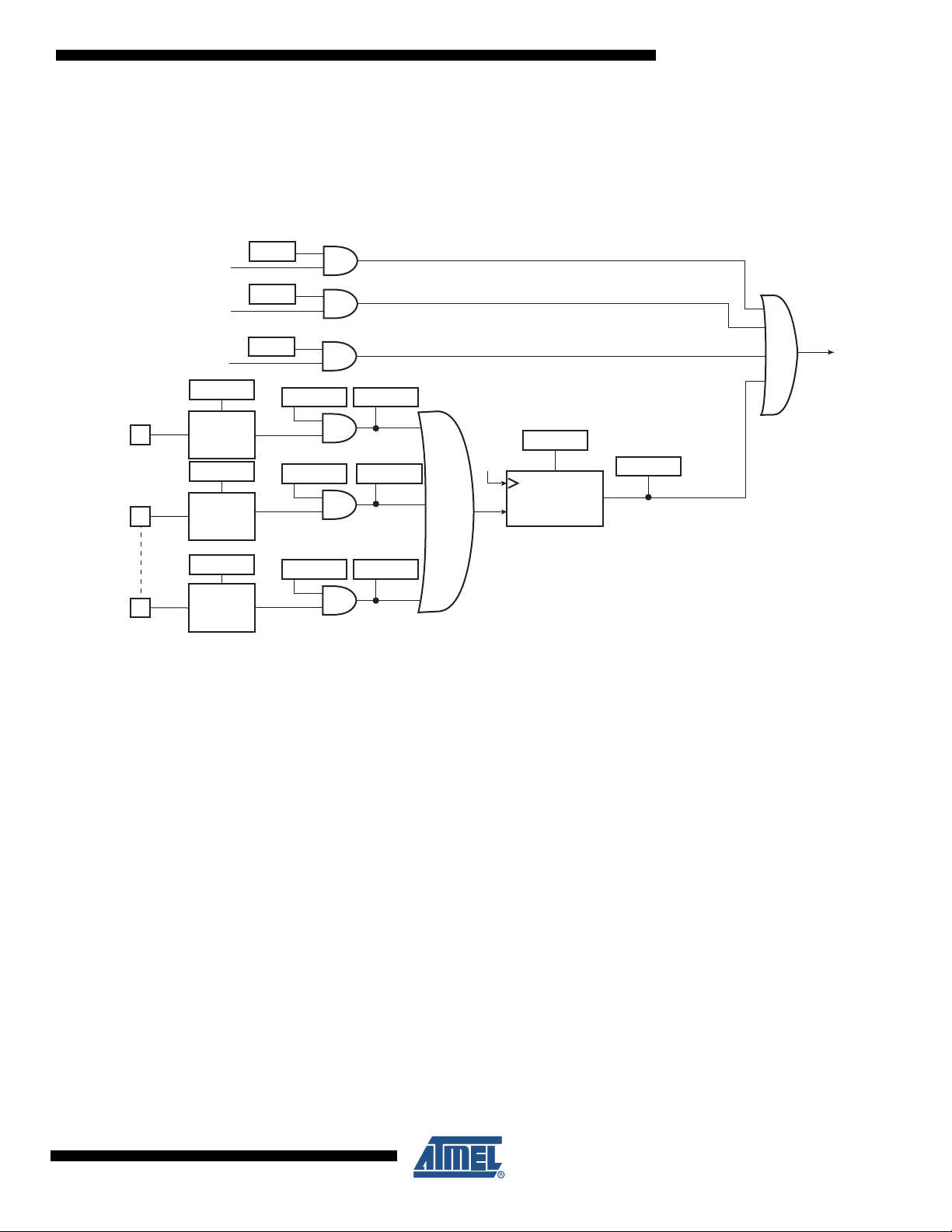
The wake-up events allow the device to exit backup mode. When a wake-up event is detected,
the Supply Controller performs a sequence which automatically reenables the core power supply and the SRAM power supply, if they are not already enabled.
Figure 5-4. Wake-up Source
SAM3N Summary
11011AS–ATARM–04-Oct-10
21
5.7 Fast Start-Up
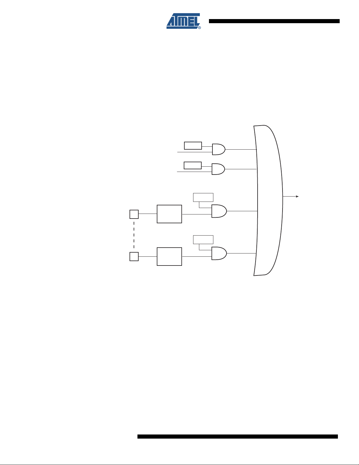
The SAM3N allows the processor to restart in a few microseconds while the processor is in wait
mode. A fast start up can occur upon detection of a low level on one of the 19 wake-up inputs
(WKUP0 to 15 + SM + RTC + RTT).
The fast restart circuitry, as shown in Figure 5-5, is fully asynchronous and provides a fast startup signal to the Power Management Controller. As soon as the fast start-up signal is asserted,
the PMC automatically restarts the embedded 4 MHz fast RC oscillator, switches the master
clock on this 4 MHz clock and reenables the processor clock.
Figure 5-5. Fast Start-Up Sources
WKUP0
WKUP15
rtc_alarm
rtt_alarm
Falling/Rising
Edge
Detector
Falling/Rising
Edge
Detector
RTCEN
RTTEN
FSTT15
FSTT0
fast_restart
22
SAM3N Summary
11011AS–ATARM–04-Oct-10
6. Input/Output Lines
The SAM3N has several kinds of input/output (I/O) lines such as general purpose I/Os (GPIO)
and system I/Os. GPIOs can have alternate functionality due to multiplexing capabilities of the
PIO controllers. The same PIO line can be used whether in IO mode or by the multiplexed
peripheral. System I/Os include pins such as test pins, oscillators, erase or analog inputs.
6.1 General Purpose I/O Lines
GPIO Lines are managed by PIO Controllers. All I/Os have several input or output modes such
as pull-up or pull-down, input Schmitt triggers, multi-drive (open-drain), glitch filters, debouncing
or input change interrupt. Programming of these modes is performed independently for each I/O
line through the PIO controller user interface. For more details, refer to the product PIO controller section.
The input output buffers of the PIO lines are supplied through VDDIO power supply rail.
The SAM3N embeds high speed pads able to handle up to 45 MHz for SPI clock lines and 35
MHz on other lines. See AC Characteristics Section in the Electrical Characteristics Section of
the datasheet for more details. Typical pull-up and pull-down value is 100 kΩ for all I/Os.
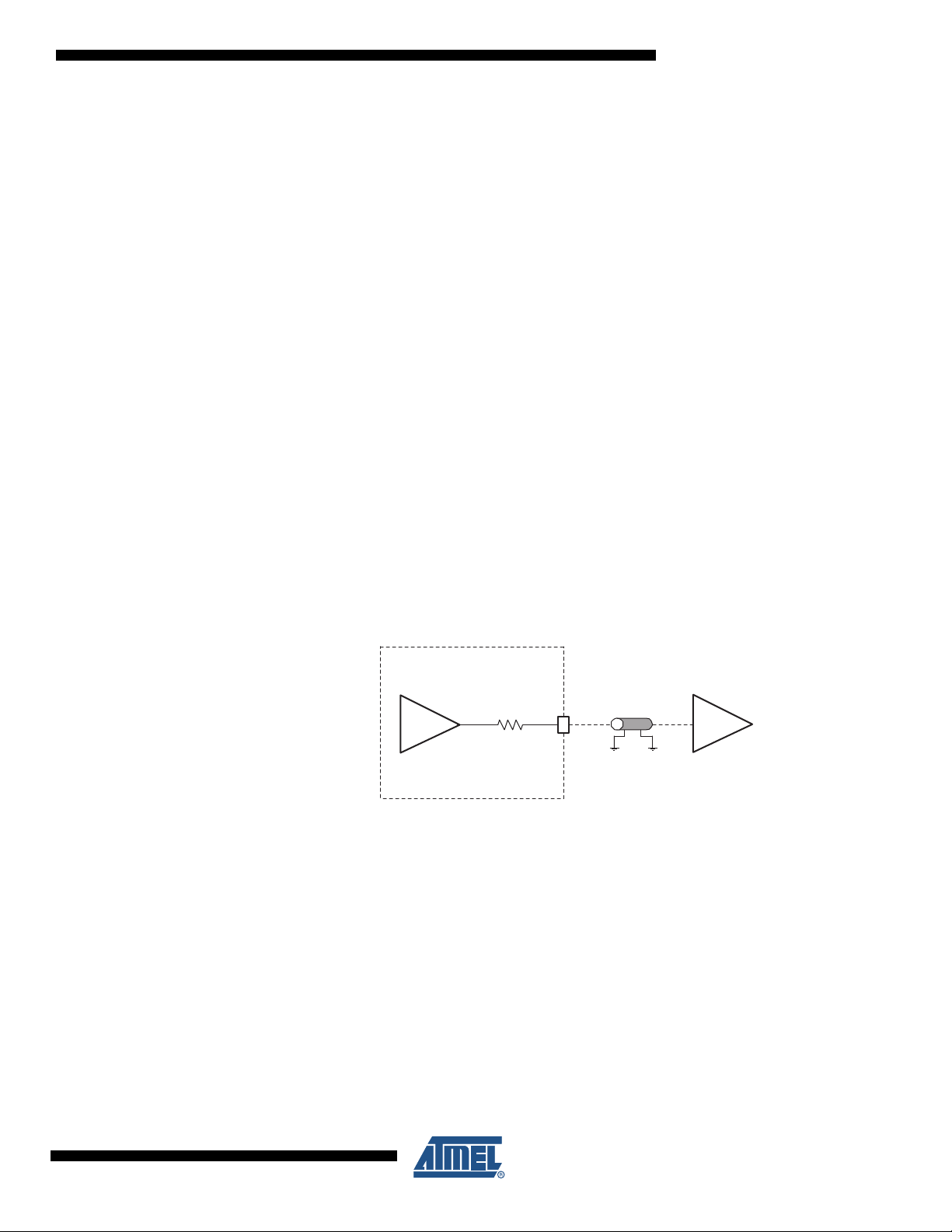
Each I/O line also embeds an ODT (On-Die Termination), (see Figure 6-1). It consists of an
internal series resistor termination scheme for impedance matching between the driver output
(SAM3N) and the PCB trace impedance preventing signal reflection. The series resistor helps to
reduce I/O switching current (di/dt) thereby reducing in turn, EMI. It also decreases overshoot
and undershoot (ringing) due to inductance of interconnect between devices or between boards.
In conclusion ODT helps diminish signal integrity issues.
SAM3N Summary
Figure 6-1. On-Die Termination
6.2 System I/O Lines
System I/O lines are pins used by oscillators, test mode, reset and JTAG to name but a few.
Described below are the SAM3N system I/O lines shared with PIO lines:
These pins are software configurable as general purpose I/O or system pins. At startup the
default function of these pins is always used.
SAM3 Driver with
Zout ~ 10 Ohms
Z0 ~ Zout + Rodt
ODT
36 Ohms Ty p.
Rodt
Receiver
PCB Trace
Z0 ~ 50 Ohms
11011AS–ATARM–04-Oct-10
23
Table 6-1. System I/O Configuration Pin List.
SYSTEM_IO
bit number
12 ERASE PB12
7 TCK/SWCLK PB7 -
6 TMS/SWDIO PB6 -
5 TDO/TRACESWO PB5 -
4 TDI PB4 -
- PA7 XIN32 -
- PA8 XOUT32 -
- PB9 XIN -
- PB8 XOUT -
Notes: 1. If PB12 is used as PIO input in user applications, a low level must be ensured at startup to prevent Flash erase before the
user application sets PB12 into PIO mode.
2. In the product Datasheet Refer to: Slow Clock Generator of the Supply Controller section.
3. In the product Datasheet Refer to: 3 to 20 MHZ Crystal Oscillator information in the PMC section.
Default function
after reset Other function
Constraints for
normal start Configuration
Low Level at
startup
(1)
In Matrix User Interface Registers
(Refer to the System I/O
Configuration Register in the Bus
Matrix section of the product
datasheet.)
See footnote
See footnote
(2)
below
(3)
below
6.2.1 Serial Wire JTAG Debug Port (SWJ-DP) Pins
The SWJ-DP pins are TCK/SWCLK, TMS/SWDIO, TDO/SWO, TDI and commonly provided on
a standard 20-pin JTAG connector defined by ARM. For more details about voltage reference
and reset state, refer to Table 3-1 on page 6.
At startup, SWJ-DP pins are configured in SWJ-DP mode to allow connection with debugging
probe. Please refer to the Debug and Test Section of the product datasheet.
SWJ-DP pins can be used as standard I/Os to provide users more general input/output pins
when the debug port is not needed in the end application. Mode selection between SWJ-DP
mode (System IO mode) and general IO mode is performed through the AHB Matrix Special
Function Registers (MATRIX_SFR). Configuration of the pad for pull-up, triggers, debouncing
and glitch filters is possible regardless of the mode.
The JTAGSEL pin is used to select the JTAG boundary scan when asserted at a high level. It
integrates a permanent pull-down resistor of about 15 kΩ to GND, so that it can be left unconnected for normal operations.
By default, the JTAG Debug Port is active. If the debugger host wants to switch to the Serial
Wire Debug Port, it must provide a dedicated JTAG sequence on TMS/SWDIO and
TCK/SWCLK which disables the JTAG-DP and enables the SW-DP. When the Serial Wire
Debug Port is active, TDO/TRACESWO can be used for trace.
The asynchronous TRACE output (TRACESWO) is multiplexed with TDO. So the asynchronous
trace can only be used with SW-DP, not JTAG-DP. For more information about SW-DP and
JTAG-DP switching, please refer to the Debug and Test Section.
24
SAM3N Summary
11011AS–ATARM–04-Oct-10

6.3 Test Pin
6.4 NRST Pin
6.5 ERASE Pin
SAM3N Summary
The TST pin is used for JTAG Boundary Scan Manufacturing Test or Fast Flash programming
mode of the SAM3N series. The TST pin integrates a permanent pull-down resistor of about 15
kΩ to GND, so that it can be left unconnected for normal operations. To enter fast programming
mode, see the Fast Flash Programming Interface (FFPI) section. For more on the manufacturing
and test mode, refer to the “Debug and Test” section of the product datasheet.
The NRST pin is bidirectional. It is handled by the on-chip reset controller and can be driven low
to provide a reset signal to the external components or asserted low externally to reset the
microcontroller. It will reset the Core and the peripherals except the Backup region (RTC, RTT
and Supply Controller). There is no constraint on the length of the reset pulse and the reset controller can guarantee a minimum pulse length. The NRST pin integrates a permanent pull-up
resistor to VDDIO of about 100 kΩ . By default, the NRST pin is configured as an input.
The ERASE pin is used to reinitialize the Flash content (and some of its NVM bits) to an erased
state (all bits read as logic level 1). It integrates a pull-down resistor of about 100 kΩ to GND, so
that it can be left unconnected for normal operations.
This pin is debounced by SCLK to improve the glitch tolerance. When the ERASE pin is tied high
during less than 100 ms, it is not taken into account. The pin must be tied high during more than
220 ms to perform a Flash erase operation.
The ERASE pin is a system I/O pin and can be used as a standard I/O. At startup, the ERASE
pin is not configured as a PIO pin. If the ERASE pin is used as a standard I/O, startup level of
this pin must be low to prevent unwanted erasing. Please refer to Section 10.2 “Peripheral Sig-
nals Multiplexing on I/O Lines” on page 41. Also, if the ERASE pin is used as a standard I/O
output, asserting the pin to low does not erase the Flash.
11011AS–ATARM–04-Oct-10
25

7. Processor and Architecture
7.1 ARM Cortex-M3 Processor
• Version 2.0
• Thumb-2 (ISA) subset consisting of all base Thumb-2 instructions, 16-bit and 32-bit.
• Harvard processor architecture enabling simultaneous instruction fetch with data load/store.
• Three-stage pipeline.
• Single cycle 32-bit multiply.
• Hardware divide.
• Thumb and Debug states.
• Handler and Thread modes.
• Low latency ISR entry and exit.
7.2 APB/AHB Bridge
The SAM3N4/2/1 product embeds one peripheral bridge:
The peripherals of the bridge are clocked by MCK.
7.3 Matrix Masters
The Bus Matrix of the SAM3N product manages 3 masters, which means that each master can
perform an access concurrently with others, to an available slave.
7.4 Matrix Slaves
Each master has its own decoder, which is defined specifically for each master. In order to simplify the addressing, all the masters have the same decodings.
Table 7-1. List of Bus Matrix Masters
Master 0 Cortex-M3 Instruction/Data
Master 1 Cortex-M3 System
Master 2 Peripheral DMA Controller (PDC)
The Bus Matrix of the SAM3N product manages 4 slaves. Each slave has its own arbiter, allowing a different arbitration per slave.
Table 7-2. List of Bus Matrix Slaves
Slave 0 Internal SRAM
Slave 1 Internal ROM
Slave 2 Internal Flash
Slave 3 Peripheral Bridge
26
SAM3N Summary
11011AS–ATARM–04-Oct-10

7.5 Master to Slave Access
All the Masters can normally access all the Slaves. However, some paths do not make sense,
for example allowing access from the Cortex-M3 S Bus to the Internal ROM. Thus, these paths
are forbidden or simply not wired, and shown as “-” in Table 7-3.
Table 7-3. SAM3N Master to Slave Access
0 Internal SRAM - X X
1 Internal ROM X - X
2 Internal Flash X - -
3 Peripheral Bridge - X X
7.6 Peripheral DMA Controller
• Handles data transfer between peripherals and memories
• Low bus arbitration overhead
– One Master Clock cycle needed for a transfer from memory to peripheral
– Two Master Clock cycles needed for a transfer from peripheral to memory
• Next Pointer management for reducing interrupt latency requirement
The Peripheral DMA Controller handles transfer requests from the channel according to the following priorities (Low to High priorities):
SAM3N Summary
Masters 0 1 2
Slaves Cortex-M3 I/D Bus Cortex-M3 S Bus PDC
Table 7-4. Peripheral DMA Controller
Instance name Channel T/R 100 & 64 Pins 48 Pins
TWI0 Transmit x x
UART0 Transmit x x
USART0 Transmit x x
DAC Transmit x N/A
SPI Transmit x x
TWI0 Receive x x
UART0 Receive x x
USART0 Receive x x
ADC Receive x x
SPI Receive x x
11011AS–ATARM–04-Oct-10
27

7.7 Debug and Test Features
• Debug access to all memory and registers in the system, including Cortex-M3 register bank
when the core is running, halted, or held in reset.
• Serial Wire Debug Port (SW-DP) and Serial Wire JTAG Debug Port (SWJ-DP) debug access
• Flash Patch and Breakpoint (FPB) unit for implementing breakpoints and code patches
• Data Watchpoint and Trace (DWT) unit for implementing watchpoints, data tracing, and
system profiling
• Instrumentation Trace Macrocell (ITM) for support of printf style debugging
• IEEE1149.1 JTAG Boundary-can on All Digital Pins
28
SAM3N Summary
11011AS–ATARM–04-Oct-10

8. Memories
Address Memory Space
Code
0x00000000
SRAM
0x20000000
Peripherals
0x40000000
0x60000000
0xA0000000
System
0xE0000000
0xFFFFFFFF
offset
ID
peripheral
block
Code
Boot Memory
0x00000000
Internal Flash
Internal ROM
0x00400000
0x00800000
0x00C00000
0x1FFFFFFF
Peripherals
0x40000000
0x40004000
SPI
21
0x40008000
0x4000C000
TC0
TC0
0x40010000
23
TC0
TC1
+0x40
24
TC0
TC2
+0x80
25
TC1
TC3
0x40014000
26
TC1
TC4
+0x40
27
TC1
TC5
+0x80
28
TWI0
19
0x40018000
TWI1
20
0x4001C000
PWM
31
0x40020000
14
0x40024000
0x40028000
0x4002C000
ADC
29
0x40038000
DACC
30
0x4003C000
0x40040000
0x40044000
0x40048000
System Controller
0x400E0000
0x400E2600
0x40100000
System Controller
0x400E0000
MATRIX
0x400E0200
PMC
5
0x400E0400
UART0
UART1
8
0x400E0600
CHIPID
0x400E0740
9
0x400E0800
EEFC
6
0x400E0A00
0x400E0C00
11
0x400E0E00
PIOB
PIOA
12
0x400E1000
PIOC
13
0x400E1200
SYSC
RSTC
0x400E1400
1
SYSC
SUPC
+0x10
SYSC
RTT
+0x30
3
SYSC
WDT
+0x50
4
SYSC
RTC
+0x60
2
SYSC
GPBR
+0x90
0x400E1600
0x4007FFFF
Reserved
Reserved
Reserved
Reserved
Reserved
Reserved
Reserved
Reserved
Reserved
Reserved
USART0
Reserved
0x40200000
Reserved
Reserved
32 MBytes
bit band alias
32 MBytes
bit band alias
0x60000000
Reserved
Reserved
USART1
15
Reserved
Reserved
0x40400000
0x20100000
0x22000000
0x24000000
Undefined
1 MByte
bit band
region
1 MByte
bit band
region
8.1 Product Mapping
Figure 8-1. SAM3N4/2/1 Product Mapping
SAM3N Summary
11011AS–ATARM–04-Oct-10
29

8.2 Embedded Memories
8.2.1 Internal SRAM
The SAM3N4 product embeds a total of 24-Kbytes high-speed SRAM.
The SAM3N2 product embeds a total of 16-Kbytes high-speed SRAM.
The SAM3N1 product embeds a total of 8-Kbytes high-speed SRAM.
The SRAM is accessible over System Cortex-M3 bus at address 0x2000 0000.
The SRAM is in the bit band region. The bit band alias region is from 0x2200 0000 and 0x23FF
FFFF.
RAM size must be configurable by calibration fuses.
8.2.2 Internal ROM
The SAM3N product embeds an Internal ROM, which contains the SAM Boot Assistant
(SAM-BA), In Application Programming routines (IAP) and Fast Flash Programming Interface
(FFPI).
At any time, the ROM is mapped at address 0x0080 0000.
8.2.3 Embedded Flash
8.2.3.1 Flash Overview
The Flash of the SAM3N4 (256 Kbytes) is organized in one bank of 1024 pages of 256 bytes
(Single plane).
The Flash of the SAM3N2 (128 Kbytes) is organized in one bank of 512 pages of 256 bytes (Single Plane).
The Flash of the SAM3N1 (64 Kbytes) is organized in one bank of 256 pages of 256 bytes (Single plane).
The Flash contains a 128-byte write buffer, accessible through a 32-bit interface.
8.2.3.2 Flash Power Supply
The Flash is supplied by VDDCORE.
8.2.3.3 Enhanced Embedded Flash Controller
The Enhanced Embedded Flash Controller (EEFC) manages accesses performed by the masters of the system. It enables reading the Flash and writing the write buffer. It also contains a
User Interface, mapped on the APB.
The Enhanced Embedded Flash Controller ensures the interface of the Flash block with the 32bit internal bus. Its 128-bit wide memory interface increases performance.
The user can choose between high performance or lower current consumption by selecting
either 128-bit or 64-bit access. It also manages the programming, erasing, locking and unlocking
sequences of the Flash using a full set of commands.
One of the commands returns the embedded Flash descriptor definition that informs the system
about the Flash organization, thus making the software generic.
30
SAM3N Summary
11011AS–ATARM–04-Oct-10

8.2.3.4 Flash Speed
8.2.3.5 Lock Regions
SAM3N Summary
The user needs to set the number of wait states depending on the frequency used.
For more details, refer to the AC Characteristics sub section in the product Electrical Characteristics Section.
Several lock bits used to protect write and erase operations on lock regions. A lock region is
composed of several consecutive pages, and each lock region has its associated lock bit.
Table 8-1. Lock bit number
Product Number of lock bits Lock region size
SAM3N4 16 16 kbytes (64 pages)
SAM3N2 8 16 kbytes (64 pages)
SAM3N1 4 16 kbytes (64 pages)
If a locked-region’s erase or program command occurs, the command is aborted and the EEFC
triggers an interrupt.
The lock bits are software programmable through the EEFC User Interface. The command “Set
Lock Bit” enables the protection. The command “Clear Lock Bit” unlocks the lock region.
Asserting the ERASE pin clears the lock bits, thus unlocking the entire Flash.
8.2.3.6 Security Bit Feature
The SAM3N features a security bit, based on a specific General Purpose NVM bit (GPNVM bit
0). When the security is enabled, any access to the Flash, either through the ICE interface or
through the Fast Flash Programming Interface, is forbidden. This ensures the confidentiality of
the code programmed in the Flash.
This security bit can only be enabled, through the command “Set General Purpose NVM Bit 0” of
the EEFC User Interface. Disabling the security bit can only be achieved by asserting the
ERASE pin at 1, after a full Flash erase is performed. When the security bit is deactivated, all
accesses to the Flash are permitted.
It is important to note that the assertion of the ERASE pin should always be longer than 200 ms.
As the ERASE pin integrates a permanent pull-down, it can be left unconnected during normal
operation. However, it is safer to connect it directly to GND for the final application.
8.2.3.7 Calibration Bits
NVM bits are used to calibrate the brownout detector and the voltage regulator. These bits are
factory configured and cannot be changed by the user. The ERASE pin has no effect on the calibration bits.
8.2.3.8 Unique Identifier
Each device integrates its own 128-bit unique identifier. These bits are factory configured and
cannot be changed by the user. The ERASE pin has no effect on the unique identifier.
11011AS–ATARM–04-Oct-10
31
8.2.3.9 Fast Flash Programming Interface
The Fast Flash Programming Interface allows programming the device through either a serial
JTAG interface or through a multiplexed fully-handshaked parallel port. It allows gang programming with market-standard industrial programmers.
The FFPI supports read, page program, page erase, full erase, lock, unlock and protect
commands.
The Fast Flash Programming Interface is enabled and the Fast Programming Mode is entered
when TST and PA0 and PA1are tied low.
8.2.3.10 SAM-BA Boot
The SAM-BA Boot is a default Boot Program which provides an easy way to program in-situ the
on-chip Flash memory.
The SAM-BA Boot Assistant supports serial communication via the UART0.
The SAM-BA Boot provides an interface with SAM-BA Graphic User Interface (GUI).
The SAM-BA Boot is in ROM and is mapped in Flash at address 0x0 when GPNVM bit 1 is set to 0.
8.2.3.11 GPNVM Bits
The SAM3N features three GPNVM bits that can be cleared or set respectively through the commands “Clear GPNVM Bit” and “Set GPNVM Bit” of the EEFC User Interface.
.
8.2.4 Boot Strategies
Table 8-2. General-purpose Non volatile Memory Bits
GPNVMBit[#] Function
0 Security bit
1 Boot mode selection
The system always boots at address 0x0. To ensure a maximum boot possibilities the memory
layout can be changed via GPNVM.
A general purpose NVM (GPNVM) bit is used to boot either on the ROM (default) or from the
Flash.
The GPNVM bit can be cleared or set respectively through the commands “Clear General-purpose NVM Bit” and “Set General-purpose NVM Bit” of the EEFC User Interface.
Setting the GPNVM Bit 1 selects the boot from the Flash, clearing it selects the boot from the
ROM. Asserting ERASE clears the GPNVM Bit 1 and thus selects the boot from the ROM by
default.
32
SAM3N Summary
11011AS–ATARM–04-Oct-10

9. System Controller
The System Controller is a set of peripherals, which allow handling of key elements of the system, such as power, resets, clocks, time, interrupts, watchdog, etc...
See the System Controller block diagram in Figure 9-1 on page 34.
SAM3N Summary
11011AS–ATARM–04-Oct-10
33
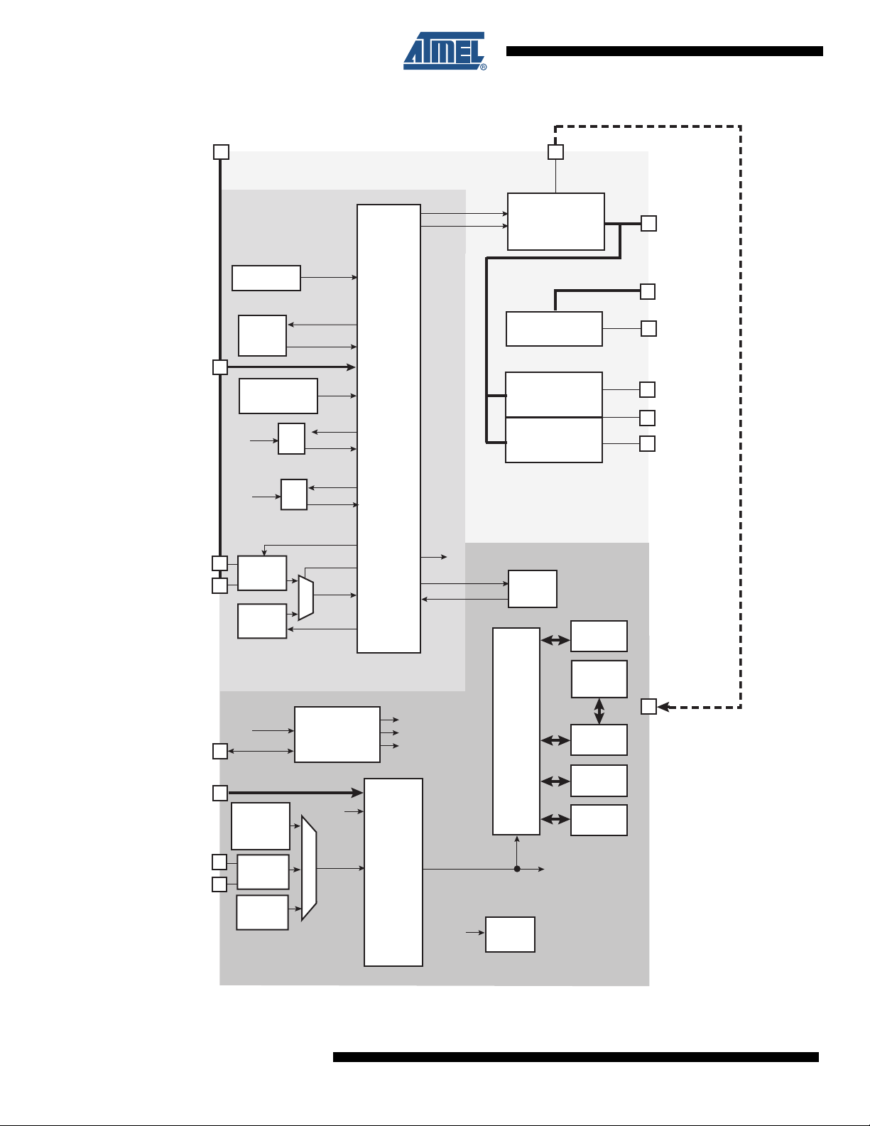
Figure 9-1. System Controller Block Diagram
Software Controlled
Voltage Regulator
ADC
PIOA/B/C
Matrix
SRAM
Cortex-M3
Flash
Peripherals
Peripheral
Bridge
Zero-Power
Power-on Reset
Supply
Monitor
(Backup)
RTC
Embedded
32 kHz RC
Oscillator
Xtal 32 kHz
Oscillator
Supply
Controller
Brownout
Detector
(Core)
General Purpose
Backup Registers
Reset
Controller
Backup Power Supply
Core Power Supply
vr_on
vr_mode
bod_on
brown_out
rtc_alarm
SLCK
rtc_nreset
proc_nreset
periph_nreset
ice_nreset
Master Clock
MCK
SLCK
core_nreset
Main Clock
MAINCK
SLCK
NRST
FSTT0 - FSTT15
XIN32
XOUT32
osc32k_xtal_en
osc32k_sel
Slow Clock
SLCK
osc32k_rc_en
core_nreset
VDDIO
VDDCORE
VDDOUT
ADVREF
ADx
WKUP0 - WKUP15
bod_core_on
lcore_brown_out
RTT
rtt_alarm
SLCK
rtt_nreset
XIN
XOUT
VDDIO
VDDIN
PIOx
DAC
DAC0
PLL
FSTT0 - FSTT15 are possible Fast Startup Sources, generated by WKUP0-WKUP15 Pins, but are not physical pins.
Embedded
12/8/4 MHz
RC
Oscillator
Xtal
Oscillator
Watchdog
Timer
Powe r
Management
Controller
34
SAM3N Summary
11011AS–ATARM–04-Oct-10

9.1 System Controller and Peripherals Mapping
Please refer to Figure 8-1, "SAM3N4/2/1 Product Mapping" on page 29.
All the peripherals are in the bit band region and are mapped in the bit band alias region.
9.2 Power-on-Reset, Brownout and Supply Monitor
The SAM3N embeds three features to monitor, warn and/or reset the chip:
• Power-on-Reset on VDDIO
• Brownout Detector on VDDCORE
• Supply Monitor on VDDIO
9.2.1 Power-on-Reset
The Power-on-Reset monitors VDDIO. It is always activated and monitors voltage at start up but
also during power down. If VDDIO goes below the threshold voltage, the entire chip is reset. For
more information, refer to the Electrical Characteristics section of the datasheet.
9.2.2 Brownout Detector on VDDCORE
The Brownout Detector monitors VDDCORE. It is active by default. It can be deactivated by software through the Supply Controller (SUPC_MR). It is especially recommended to disable it
during low-power modes such as wait or sleep modes.
SAM3N Summary
If VDDCORE goes below the threshold voltage, the reset of the core is asserted. For more information, refer to the Supply Controller (SUPC) and Electrical Characteristics sections of the
datasheet.
9.2.3 Supply Monitor on VDDIO
The Supply Monitor monitors VDDIO. It is inactive by default. It can be activated by software and
is fully programmable with 16 steps for the threshold (between 1.9V to 3.4V). It is controlled by
the Supply Controller (SUPC). A sample mode is possible. It allows to divide the supply monitor
power consumption by a factor of up to 2048. For more information, refer to the SUPC and Electrical Characteristics sections of the datasheet.
9.3 Reset Controller
The Reset Controller is based on a Power-on-Reset cell, and a Supply Monitor on VDDCORE.
The Reset Controller is capable to return to the software the source of the last reset, either a
general reset, a wake-up reset, a software reset, a user reset or a watchdog reset.
The Reset Controller controls the internal resets of the system and the NRST pin input/output. It
is capable to shape a reset signal for the external devices, simplifying to a minimum connection
of a push-button on the NRST pin to implement a manual reset.
The configuration of the Reset Controller is saved as supplied on VDDIO.
9.4 Supply Controller (SUPC)
The Supply Controller controls the power supplies of each section of the processor and the
peripherals (via Voltage regulator control)
11011AS–ATARM–04-Oct-10
The Supply Controller has its own reset circuitry and is clocked by the 32 kHz slow clock
generator.
35
The reset circuitry is based on a zero-power power-on reset cell and a brownout detector cell.
XIN
XOUT
Main Clock
MAINCK
Slow Clock
SLCK
XIN32
XOUT32
Clock Generator
XTALSEL
MAINSEL
Power
Management
Controller
ControlStatus
PLL and
Divider A
PLLA Clock
PLLACK
3-20 MHz
Main
Oscillator
Slow Clock
Oscillator
On Chip
12/8/4 MHz
RC OSC
On Chip 32 kHz
RC OSC
The zero-power power-on reset allows the Supply Controller to start properly, while the software-programmable brownout detector allows detection of either a battery discharge or main
voltage loss.
The Slow Clock generator is based on a 32 kHz crystal oscillator and an embedded 32 kHz RC
oscillator. The Slow Clock defaults to the RC oscillator, but the software can enable the crystal
oscillator and select it as the Slow Clock source.
The Supply Controller starts up the device by sequentially enabling the internal power switches
and the Voltage Regulator, then it generates the proper reset signals to the core power supply.
It also enables to set the system in different low power modes and to wake it up from a wide
range of events.
9.5 Clock Generator
The Clock Generator is made up of:
• One Low Power 32768Hz Slow Clock Oscillator with bypass mode
• One Low-Power RC Oscillator
• One 3-20 MHz Crystal or Ceramic resonator Oscillator, which can be bypassed
• One Fast RC Oscillator factory programmed, 3 output frequencies can be selected: 4, 8 or 12
MHz. By default 4 MHz is selected.
• One 60 to 130 MHz programmable PLL, capable to provide the clock MCK to the processor
and to the peripherals. The input frequency of PLL is from 3.5 to 20 MHz.
Figure 9-2. Clock Generator Block Diagram
36
SAM3N Summary
11011AS–ATARM–04-Oct-10
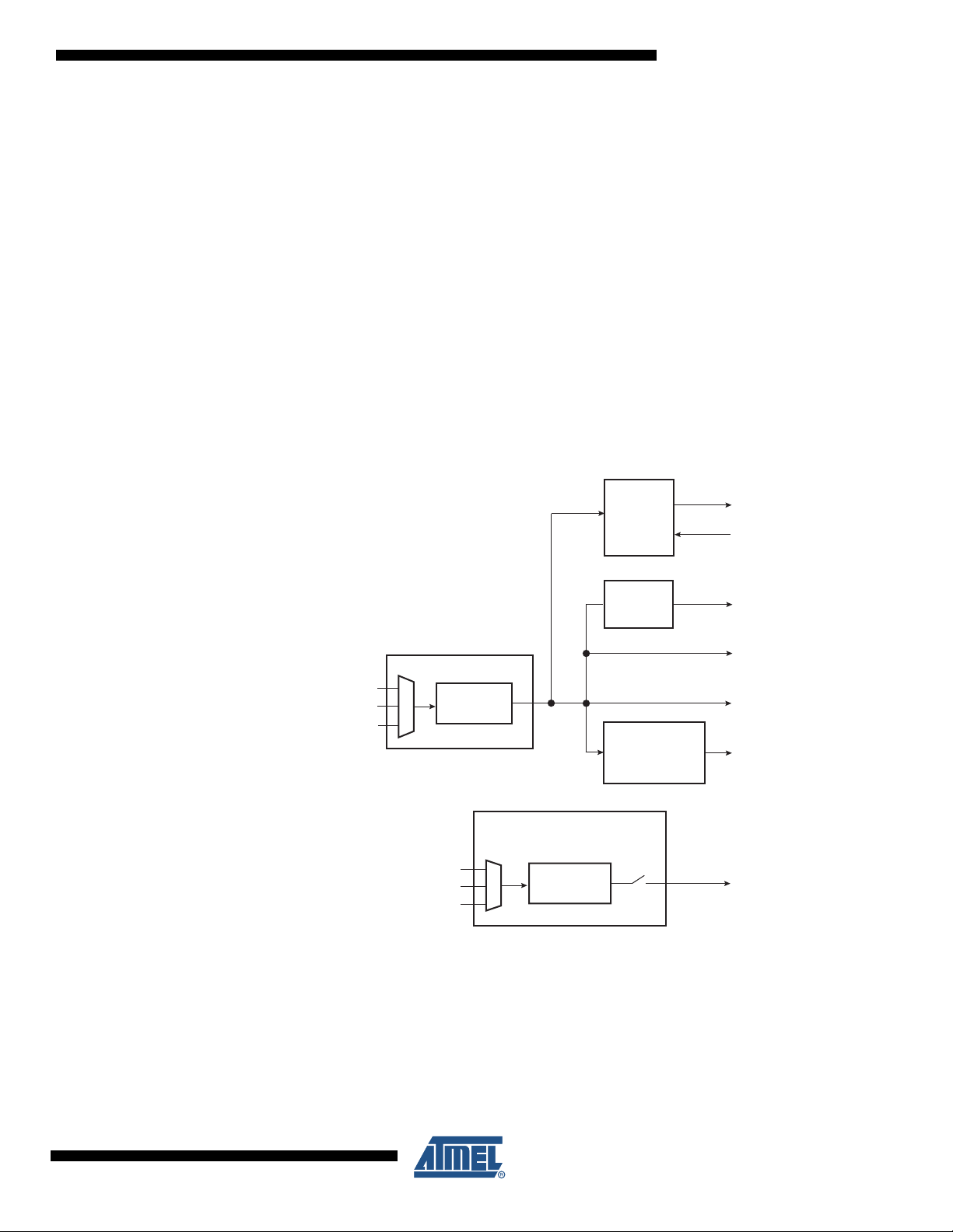
9.6 Power Management Controller
MCK
periph_clk[..]
int
SLCK
MAINCK
Prescaler
/1,/2,/4,..,/64
HCK
Processor
Clock
Controller
Sleep Mode
Master Clock Controller
Peripherals
Clock Controller
ON/OFF
SLCK
MAINCK
Prescaler
/1,/2,/4,..,/64
Programmable Clock Controller
pck[..]
ON/OFF
FCLK
SystTick
Divider
/8
PLLCK
PLLCK
The Power Management Controller provides all the clock signals to the system. It provides:
• the Processor Clock HCLK
• the Free running processor clock FCLK
• the Cortex SysTick external clock
• the Master Clock MCK, in particular to the Matrix and the memory interfaces
• independent peripheral clocks, typically at the frequency of MCK
• three programmable clock outputs: PCK0, PCK1 and PCK2
The Supply Controller selects between the 32 kHz RC oscillator or the crystal oscillator. The
unused oscillator is disabled automatically so that power consumption is optimized.
By default, at startup the chip runs out of the Master Clock using the Fast RC Oscillator running
at 4 MHz.
The user can trim by software the 8 and 12 MHz RC Oscillator frequency.
Figure 9-3. SAM3N4/2/1 Power Management Controller Block Diagram
SAM3N Summary
The SysTick calibration value is fixed at 6000 which allows the generation of a time base of 1 ms
with SysTick clock at 6 MHz (48 MHz/8)
9.7 Watchdog Timer
11011AS–ATARM–04-Oct-10
• 16-bit key-protected only-once-Programmable Counter
• Windowed, prevents the processor to be in a dead-lock on the watchdog access
37

9.8 SysTick Timer
9.9 Real-time Timer
9.10 Real Time Clock
• 24-bit down counter
• Self-reload capability
• Flexible System timer
• Real-time Timer, allowing backup of time with different accuracies
– 32-bit Free-running back-up Counter
– Integrates a 16-bit programmable prescaler running on slow clock
– Alarm register capable to generate a wake-up of the system through the Shut Down
Controller
• Low power consumption
• Full asynchronous design
• Two hundred year calendar
• Programmable Periodic Interrupt
• Alarm and update parallel load
• Control of alarm and update Time/Calendar Data In
9.11 General Purpose Backup Registers
• Eight 32-bit general-purpose backup registers
9.12 Nested Vectored Interrupt Controller
• Thirty Two maskable external interrupts
• Sixteen priority levels
• Processor state automatically saved on interrupt entry, and restored on
• Dynamic reprioritization of interrupts
• Priority grouping
– selection of pre-empting interrupt levels and non pre-empting interrupt levels
• Support for tail-chaining and late arrival of interrupts
– back-to-back interrupt processing without the overhead of state saving and
restoration between interrupts.
• Processor state automatically saved on interrupt entry and restored on interrupt exit, with no
instruction overhead
38
SAM3N Summary
11011AS–ATARM–04-Oct-10

9.13 Chip Identification
• Chip Identifier (CHIPID) registers permit recognition of the device and its revision.
Table 9-1. SAM3N Chip ID Register
• JTAG ID: 0x05B2E03F
SAM3N Summary
Chip Name CHIPID_CIDR CHIPID_EXID
ATSAM3N4C (Rev A) 0x29540960 0x0
ATSAM3N2C (Rev A) 0x29590760 0x0
ATSAM3N1C (Rev A) 0x29580560 0x0
ATSAM3N4B (Rev A) 0x29440960 0x0
ATSAM3N2B (Rev A) 0x29490760 0x0
ATSAM3N1B (Rev A) 0x29480560 0x0
ATSAM3N4A (Rev A) 0x29340960 0x0
ATSAM3N2A (Rev A) 0x29390760 0x0
ATSAM3N1A (Rev A) 0x29380560 0x0
9.14 UART
9.15 PIO Controllers
•Two-pin UART
– Implemented features are 100% compatible with the standard Atmel USART
– Independent receiver and transmitter with a common programmable Baud Rate
Generator
– Even, Odd, Mark or Space Parity Generation
– Parity, Framing and Overrun Error Detection
– Automatic Echo, Local Loopback and Remote Loopback Channel Modes
– Support for two PDC channels with connection to receiver and transmitter
• 3 PIO Controllers, PIOA, PIOB and PIOC (100-pin version only) controlling a maximum of 79
I/O Lines
• Each PIO Controller controls up to 32 programmable I/O Lines
• Fully programmable through Set/Clear Registers
Table 9-2. PIO available according to pin count
Version 48 pin 64 pin 100 pin
PIOA 21 32 32
PIOB 13 15 15
PIOC --32
11011AS–ATARM–04-Oct-10
• Multiplexing of four peripheral functions per I/O Line
• For each I/O Line (whether assigned to a peripheral or used as general purpose I/O)
– Input change, rising edge, falling edge, low level and level interrupt
– Debouncing and Glitch filter
39

– Multi-drive option enables driving in open drain
– Programmable pull up on each I/O line
– Pin data status register, supplies visibility of the level on the pin at any time
• Selection of the drive level
• Synchronous output, provides Set and Clear of several I/O lines in a single write
10. Peripherals
10.1 Peripheral Identifiers
Table 10-1 defines the Peripheral Identifiers of the SAM3N4/2/1. A peripheral identifier is
required for the control of the peripheral interrupt with the Nested Vectored Interrupt Controller
and for the control of the peripheral clock with the Power Management Controller.
Table 10-1. Peripheral Identifiers
Instance ID Instance Name NVIC Interrupt PMC Clock Control Instance Description
0 SUPC X Supply Controller
1 RSTC X Reset Controller
2 RTC X Real Time Clock
3 RTT X Real Time Timer
4 WDT X Watchdog Timer
5 PMC X Power Management Controller
6 EEFC X Enhanced Flash Controller
7 - - Reserved
8 UART0 XXUART 0
9 UART1 XXUART 1
10 - --Reserved
11 PIOA XXParallel I/O Controller A
12 PIOB XXParallel I/O Controller B
13 PIOC XXParallel I/O Controller C
14 USART0 XXUSART 0
15 USART1 XXUSART 1
16 - --Reserved
17 - --Reserved
18 - --Reserved
19 TWI0 XXTwo Wire Interface 0
20 TWI1 XXTwo Wire Interface 1
21 SPI XXSerial Peripheral Interface
22 - --Reserved
23 TC0 XXTimer/Counter 0
40
24 TC1 XX
Timer/Counter 1
SAM3N Summary
11011AS–ATARM–04-Oct-10

SAM3N Summary
Table 10-1. Peripheral Identifiers (Continued)
Instance ID Instance Name NVIC Interrupt PMC Clock Control Instance Description
25 TC2 XXTimer/Counter 2
26 TC3 XXTimer/Counter 3
27 TC4 XXTimer/Counter 4
28 TC5 XXTimer/Counter 5
29 ADC XXAnalog-to-Digital Converter
30 DACC XXDigital-to-Analog Converter
31 PWM XXPulse Width Modulation
10.2 Peripheral Signals Multiplexing on I/O Lines
The SAM3N product features 2 PIO controllers (48-pin and 64-pin version) or 3 PIO controllers
(100-pin version), PIOA, PIOB and PIOC, that multiplex the I/O lines of the peripheral set.
The SAM3N 64-pin and 100-pin PIO Controller controls up to 32 lines (see Table 9-2, “PIO avail-
able according to pin count,” on page 39). Each line can be assigned to one of three peripheral
functions: A, B or C. The multiplexing tables in the following paragraphs define how the I/O lines
of the peripherals A, B and C are multiplexed on the PIO Controllers. The column “Comments”
has been inserted in this table for the user’s own comments; it may be used to track how pins
are defined in an application.
Note that some peripheral functions which are output only, might be duplicated within the tables.
11011AS–ATARM–04-Oct-10
41

10.2.1 PIO Controller A Multiplexing
Table 10-2. Multiplexing on PIO Controller A (PIOA)
I/O Line Peripheral A Peripheral B Peripheral C Extra Function System Function Comments
PA0 PWM0 TIOA0 WKUP0 High drive
PA1 PWM1 TIOB0 WKUP1 High drive
PA2 PWM2 SCK0 DATRG WKUP2 High drive
PA 3 T WD 0 N P C S3 High drive
PA4 TWCK0 TCLK0 WKUP3
PA5 RXD0 NPCS3 WKUP4
PA 6 T X D 0 P C K0
PA 7 R T S0 P W M 3 X IN 3 2
PA8 CTS0 ADTRG WKUP5 XOUT32
PA9 URXD0 NPCS1 WKUP6
PA10 UTXD0 NPCS2
PA11 NPCS0 PWM0 WKUP7
PA12 MISO PWM1
PA13 MOSI PWM2
PA14 SPCK PWM3 WKUP8
PA15 TIOA1 WKUP14
PA16 TIOB1 WKUP15
PA17 PCK1 AD0
PA18 PCK2 AD1
PA19 AD2/WKUP9
PA20 AD3/WKUP10
PA21 RXD1 PCK1 AD8 64/100-pin versions
PA22 TXD1 NPCS3 AD9 64/100-pin versions
PA23 SCK1 PWM0 64/100-pin versions
PA24 RTS1 PWM1 64/100-pin versions
PA25 CTS1 PWM2 64/100-pin versions
PA26 TIOA2 64/100-pin versions
PA27 TIOB2 64/100-pin versions
PA28 TCLK1 64/100-pin versions
PA29 TCLK2 64/100-pin versions
PA30 NPCS2 WKUP11 64/100-pin versions
PA31 NPCS1 PCK2 64/100-pin versions
42
SAM3N Summary
11011AS–ATARM–04-Oct-10

SAM3N Summary
10.2.2 PIO Controller B Multiplexing
Table 10-3. Multiplexing on PIO Controller B (PIOB)
I/O Line Peripheral A Peripheral B Peripheral C Extra Function System Function Comments
PB0 PWM0 AD4
PB1 PWM1 AD5
PB2 URXD1 NPCS2 AD6/WKUP12
PB3 UTXD1 PCK2 AD7
PB4 TWD1 PWM2 TDI
PB5 TWCK1 WKUP13
PB6 TMS/SWDIO
PB7 TCK/SWCLK
PB8 XOUT
PB9 XIN
PB10
PB11
PB12 ERASE
PB13 PCK0 DAC0 64/100-pin versions
PB14 NPCS1 PWM3 64/100-pin versions
TDO/
TRACESWO
11011AS–ATARM–04-Oct-10
43

10.2.3 PIO Controller C Multiplexing
I/O Line Peripheral A Peripheral B Peripheral C Extra Function System Function Comments
PC0 100-pin version
PC1 100-pin version
PC2 100-pin version
PC3 100-pin version
PC4 NPCS1 100-pin version
PC5 100-pin version
PC6 100-pin version
PC7 NPCS2 100-pin version
PC8 PWM0 100-pin version
PC9 PWM1 100-pin version
PC10 PWM2 100-pin version
PC11 PWM3 100-pin version
PC12 AD12 100-pin version
PC13 AD10 100-pin version
PC14 PCK2 100-pin version
PC15 AD11 100-pin version
PC16 PCK0 100-pin version
PC17 PCK1 100-pin version
PC18 PWM0 100-pin version
PC19 PWM1 100-pin version
PC20 PWM2 100-pin version
PC21 PWM3 100-pin version
PC22 PWM0 100-pin version
PC23 TIOA3 100-pin version
PC24 TIOB3 100-pin version
PC25 TCLK3 100-pin version
PC26 TIOA4 100-pin version
PC27 TIOB4 100-pin version
PC28 TCLK4 100-pin version
PC29 TIOA5 AD13 100-pin version
PC30 TIOB5 AD14 100-pin version
PC31 TCLK5 AD15 100-pin version
44
SAM3N Summary
11011AS–ATARM–04-Oct-10

11. Embedded Peripherals Overview
11.1 Serial Peripheral Interface (SPI)
• Supports communication with serial external devices
– Four chip selects with external decoder support allow communication with up to 15
peripherals
– Serial memories, such as DataFlash and 3-wire EEPROMs
– Serial peripherals, such as ADCs, DACs, LCD Controllers, CAN Controllers and
Sensors
– External co-processors
• Master or slave serial peripheral bus interface
– 8- to 16-bit programmable data length per chip select
– Programmable phase and polarity per chip select
– Programmable transfer delays between consecutive transfers and between clock
and data per chip select
– Programmable delay between consecutive transfers
– Selectable mode fault detection
• Very fast transfers supported
– Transfers with baud rates up to MCK
– The chip select line may be left active to speed up transfers on the same device
SAM3N Summary
11.2 Two Wire Interface (TWI)
• Master, Multi-Master and Slave Mode Operation
• Compatibility with Atmel two-wire interface, serial memory and I
• One, two or three bytes for slave address
• Sequential read/write operations
• Bit Rate: Up to 400 kbit/s
• General Call Supported in Slave Mode
• Connecting to PDC channel capabilities optimizes data transfers in Master Mode only (for
TWI0 only)
– One channel for the receiver, one channel for the transmitter
– Next buffer support
11.3 Universal Asynchronous Receiver Transceiver (UART)
•Two-pin UART
– Implemented features are 100% compatible with the standard Atmel USART
– Independent receiver and transmitter with a common programmable Baud Rate
Generator
– Even, Odd, Mark or Space Parity Generation
– Parity, Framing and Overrun Error Detection
– Automatic Echo, Local Loopback and Remote Loopback Channel Modes
2
C compatible devices
11011AS–ATARM–04-Oct-10
45

11.4 USART
– Support for two PDC channels with connection to receiver and transmitter (for
UART0 only)
• Programmable Baud Rate Generator
• 5- to 9-bit full-duplex synchronous or asynchronous serial communications
– 1, 1.5 or 2 stop bits in Asynchronous Mode or 1 or 2 stop bits in Synchronous Mode
– Parity generation and error detection
– Framing error detection, overrun error detection
– MSB- or LSB-first
– Optional break generation and detection
– By 8 or by-16 over-sampling receiver frequency
– Hardware handshaking RTS-CTS
– Receiver time-out and transmitter timeguard
– Optional Multi-drop Mode with address generation and detection
• RS485 with driver control signal
• ISO7816, T = 0 or T = 1 Protocols for interfacing with smart cards (Only on USART0)
– NACK handling, error counter with repetition and iteration limit
• SPI Mode
–Master or Slave
– Serial Clock programmable Phase and Polarity
– SPI Serial Clock (SCK) Frequency up to MCK/4
• IrDA modulation and demodulation (Only on USART0)
– Communication at up to 115.2 Kbps
• Test Modes
– Remote Loopback, Local Loopback, Automatic Echo
• PDC support (for USART0 only)
11.5 Timer Counter (TC)
• Six 16-bit Timer Counter Channels
• Wide range of functions including:
• Each channel is user-configurable and contains:
46
SAM3N Summary
– Frequency Measurement
– Event Counting
– Interval Measurement
– Pulse Generation
–Delay Timing
– Pulse Width Modulation
– Up/down Capabilities
– Three external clock inputs
– Five internal clock inputs
11011AS–ATARM–04-Oct-10

– Two multi-purpose input/output signals
• Two global registers that act on all three TC Channels
• Quadrature decoder
– Advanced line filtering
– Position/revolution/speed
• 2-bit Gray Up/Down Counter for Stepper Motor
11.6 Pulse Width Modulation Controller (PWM)
• Four channels, one 16-bit counter per channel
• Common clock generator, providing thirteen different clocks
– One Modulo n counter providing eleven clocks
– Two independent linear dividers working on modulo n counter outputs
• Independent channel programming
– Independent enable/disable commands
– Independent clock selection
– Independent period and duty cycle, with double buffering
– Programmable selection of the output waveform polarity
SAM3N Summary
11.7 10-bit Analog-to-Digital Converter
• Up to 16-channel ADC
• 10-bit 384 Ksamples/sec. or 8-bit 583 Ksamples/sec. Successive Approximation Register
ADC
• ±2 LSB Integral Non Linearity, ±1 LSB Differential Non Linearity
• Integrated 8-to-1 multiplexer, offering eight independent 3.3V analog inputs
• External voltage reference for better accuracy on low voltage inputs
• Individual enable and disable of each channel
• Multiple trigger source
– Hardware or software trigger
– External trigger pin
– Timer Counter 0 to 2 outputs TIOA0 to TIOA2 trigger
• Sleep Mode and conversion sequencer
– Automatic wakeup on trigger and back to sleep mode after conversions of all
enabled channels
11.8 Digital-to-Analog Converter (DAC)
• 1 channel 10-bit DAC
• Up to 500 ksamples/s conversion rate
• Flexible conversion range
• Multiple trigger sources
• One PDC channel
11011AS–ATARM–04-Oct-10
47
12. Package Drawings
Note : 1. This drawing is for general information only. Refer to JEDEC Drawing MS-026 for additional information.
The SAM3N series devices are available in LQFP, QFN and LFBGA packages.
Figure 12-1. 100-lead LQFP Package Drawing
48
SAM3N Summary
11011AS–ATARM–04-Oct-10
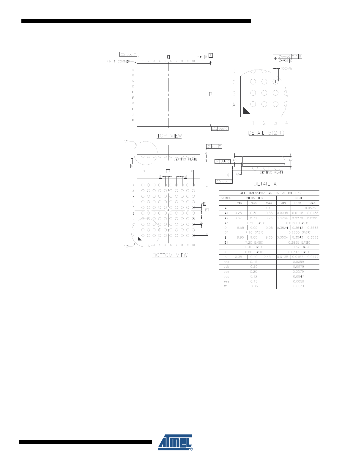
Figure 12-2. 100-ball LFBGA Package Drawing
SAM3N Summary
11011AS–ATARM–04-Oct-10
49
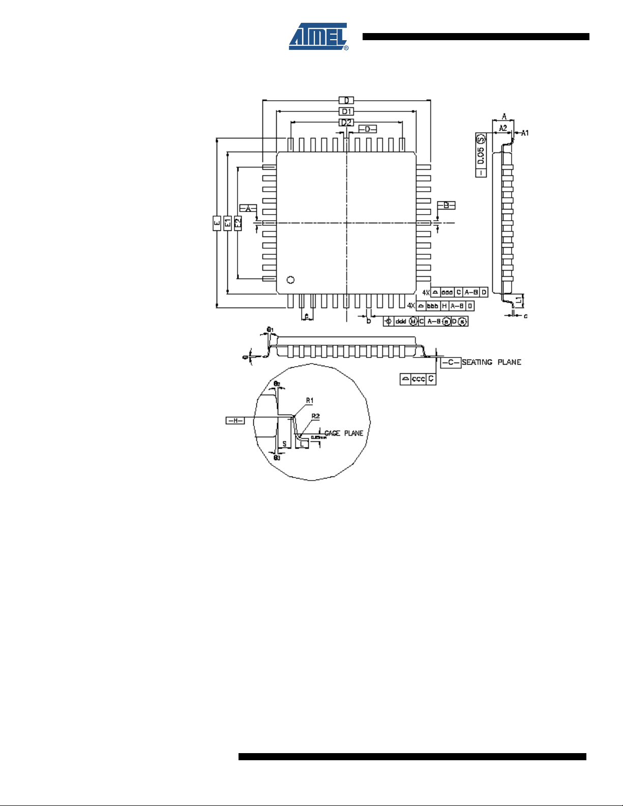
Figure 12-3. 64- and 48-lead LQFP Package Drawing
50
SAM3N Summary
11011AS–ATARM–04-Oct-10
Table 12-1. 48-lead LQFP Package Dimensions (in mm)
SAM3N Summary
Symbol
A – –1.60– –0.063
A1 0.05 – 0.15 0.002 – 0.006
A2 1.35 1.40 1.45 0.053 0.055 0.057
D 9.00 BSC 0.354 BSC
D1 7.00 BSC 0.276 BSC
E 9.00 BSC 0.354 BSC
E1 7.00 BSC 0.276 BSC
R2 0.08 – 0.20 0.003 – 0.008
R1 0.08 – – 0.003 – –
q 0°3.5°7° 0°3.5°7°
θ
1
θ
2
θ
3
c 0.09 – 0.20 0.004 – 0.008
L 0.45 0.60 0.75 0.018 0.024 0.030
L1 1.00 REF 0.039 REF
S 0.20 – – 0.008 – –
b 0.17 0.20 0.27 0.007 0.008 0.011
Min Nom Max Min Nom Max
0°––0°––
11° 12° 13° 11° 12° 13°
11° 12° 13° 11° 12° 13°
Millimeter Inch
e 0.50 BSC. 0.020 BSC.
D2 5.50 0.217
E2 5.50 0.217
Tolerances of Form and Position
aaa 0.20 0.008
bbb 0.20 0.008
ccc 0.08 0.003
ddd 0.08 0.003
11011AS–ATARM–04-Oct-10
51
Table 12-2. 64-lead LQFP Package Dimensions (in mm)
Symbol
A – –1.60– –0.063
A1 0.05 – 0.15 0.002 – 0.006
A2 1.35 1.40 1.45 0.053 0.055 0.057
D 12.00 BSC 0.472 BSC
D1 10.00 BSC 0.383 BSC
E 12.00 BSC 0.472 BSC
E1 10.00 BSC 0.383 BSC
R2 0.08 – 0.20 0.003 – 0.008
R1 0.08 – – 0.003 – –
q 0°3.5°7° 0°3.5°7°
θ
1
θ
2
θ
3
c 0.09 – 0.20 0.004 – 0.008
L 0.45 0.60 0.75 0.018 0.024 0.030
L1 1.00 REF 0.039 REF
S 0.20 – – 0.008 – –
b 0.17 0.20 0.27 0.007 0.008 0.011
e 0.50 BSC. 0.020 BSC.
D2 7.50 0.285
E2 7.50 0.285
aaa 0.20 0.008
bbb 0.20 0.008
ccc 0.08 0.003
ddd 0.08 0.003
Min Nom Max Min Nom Max
0°––0°––
11° 12° 13° 11° 12° 13°
11° 12° 13° 11° 12° 13°
Millimeter Inch
Tolerances of Form and Position
52
SAM3N Summary
11011AS–ATARM–04-Oct-10
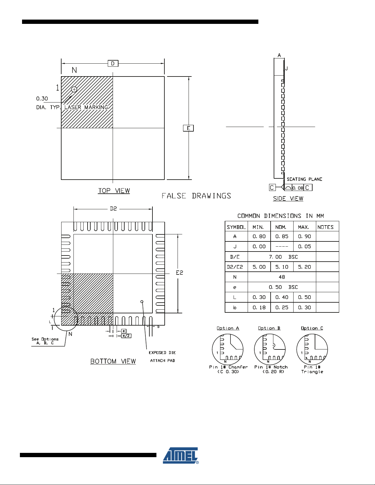
Figure 12-4. 48-pad QFN Package Drawing
SAM3N Summary
11011AS–ATARM–04-Oct-10
53
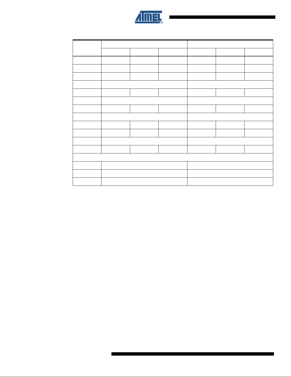
Table 12-3. 48-pad QFN Package Dimensions (in mm)
Symbol
Min Nom Max Min Nom Max
A – – 090 – – 0.035
A1 – – 0.050 – – 0.002
A2 – 0.65 0.70 – 0.026 0.028
A3 0.20 REF 0.008 REF
b 0.18 0.20 0.23 0.007 0.008 0.009
D 7.00 bsc 0.276 bsc
D2 5.45 5.60 5.75 0.215 0.220 0.226
E 7.00 bsc 0.276 bsc
E2 5.45 5.60 5.75 0.215 0.220 0.226
L 0.35 0.40 0.45 0.014 0.016 0.018
e 0.50 bsc 0.020 bsc
R 0.09 – – 0.004 – –
aaa 0.10 0.004
bbb 0.10 0.004
ccc 0.05 0.002
Millimeter Inch
Tolerances of Form and Position
54
SAM3N Summary
11011AS–ATARM–04-Oct-10
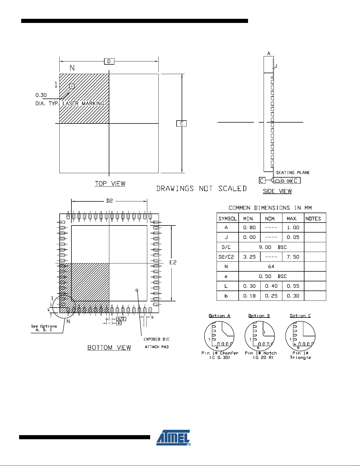
Figure 12-5. 64-pad QFN Package Drawing
SAM3N Summary
11011AS–ATARM–04-Oct-10
55

13. Ordering Information
Table 13-1. SAM3N4/2/1
Flash
Ordering Code MRL
ATSAM3N4CA-AU A 256 QFP100 Green
ATSAM3N4CA-CU A 256 BGA100 Green
ATSAM3N4BA-AU A 256 QFP64 Green
ATSAM3N4BA-MU A 256 QFN64 Green
ATSAM3N4AA-AU A 256 QFP48 Green
ATSAM3N4AA-MU A 256 QFN48 Green
ATSAM3N2CA-AU A 128 QFP100 Green
ATSAM3N2CA-CU A 128 BGA100 Green
ATSAM3N2BA-AU A 128 QFP64 Green
ATSAM3N2BA-MU A 128 QFN64 Green
ATSAM3N2AA-AU A 128 QFP48 Green
ATSAM3N2AA-MU A 128 QFN48 Green
ATSAM3N1CA-AU A 64 QFP100 Green
ATSAM3N1CA-CU A 64 BGA100 Green
ATSAM3N1BA-AU A 64 QFP64 Green
ATSAM3N1BA-MU A 64 QFN64 Green
ATSAM3N1AA-AU A 64 QFP48 Green
ATSAM3N1AA-MU A 64 QFN48 Green
(Kbytes) Package (Kbytes) Package Type
Temperature
Operating Range
Industrial
-40°C to 85°C
Industrial
-40°C to 85°C
Industrial
-40°C to 85°C
Industrial
-40°C to 85°C
Industrial
-40°C to 85°C
Industrial
-40°C to 85°C
Industrial
-40°C to 85°C
Industrial
-40°C to 85°C
Industrial
-40°C to 85°C
Industrial
-40°C to 85°C
Industrial
-40°C to 85°C
Industrial
-40°C to 85°C
Industrial
-40°C to 85°C
Industrial
-40°C to 85°C
Industrial
-40°C to 85°C
Industrial
-40°C to 85°C
Industrial
-40°C to 85°C
Industrial
-40°C to 85°C
56
SAM3N Summary
11011AS–ATARM–04-Oct-10

Revision History
Doc. Rev Comments
11011AS First issue
SAM3N Summary
Change
Request Ref.
11011AS–ATARM–04-Oct-10
57

Headquarters International
Atmel Corporation
2325 Orchard Parkway
San Jose, CA 95131
USA
Tel: 1(408) 441-0311
Fax: 1(408) 487-2600
Atmel Asia
Unit 1-5 & 16, 19/F
BEA Tower, Millennium City 5
418 Kwun Tong Road
Kwun Tong, Kowloon
Hong Kong
Tel: (852) 2245-6100
Fax: (852) 2722-1369
Product Contact
Web Site
www.atmel.com
www.atmel.com/AT91SAM
Literature Requests
www.atmel.com/literature
Atmel Europe
Le Krebs
8, Rue Jean-Pierre Timbaud
BP 309
78054 Saint-Quentin-enYvelines Cedex
France
Tel: (33) 1-30-60-70-00
Fax: (33) 1-30-60-71-11
Technical Support
AT91SAM Support
Atmel techincal support
Atmel Japan
9F, Tonetsu Shinkawa Bldg.
1-24-8 Shinkawa
Chuo-ku, Tokyo 104-0033
Japan
Tel: (81) 3-3523-3551
Fax: (81) 3-3523-7581
Sales Contacts
www.atmel.com/contacts/
Disclaimer: The information in this document is provided in connection with Atmel products. No license, express or implied, by estoppel or otherwise, to any
intellectual property right is granted by this document or in connection with the sale of Atmel products. EXCEPT AS SET FORTH IN ATMEL’S TERMS AND CONDI-
TIONS OF SALE LOCATED ON ATMEL’S WEB SITE, ATMEL ASSUMES NO LIABILITY WHATSOEVER AND DISCLAIMS ANY EXPRESS, IMPLIED OR STATUTORY
WARRANTY RELATING TO ITS PRODUCTS INCLUDING, BUT NOT LIMITED TO, THE IMPLIED WARRANTY OF MERCHANTABILITY, FITNESS FOR A PARTICULAR
PURPOSE, OR NON-INFRINGEMENT. IN NO EVENT SHALL ATMEL BE LIABLE FOR ANY DIRECT, INDIRECT, CONSEQUENTIAL, PUNITIVE, SPECIAL OR INCIDENTAL DAMAGES (INCLUDING, WITHOUT LIMITATION, DAMAGES FOR LOSS OF PROFITS, BUSINESS INTERRUPTION, OR LOSS OF INFORMATION) ARISING OUT
OF THE USE OR INABILITY TO USE THIS DOCUMENT, EVEN IF ATMEL HAS BEEN ADVISED OF THE POSSIBILITY OF SUCH DAMAGES. Atmel makes no
representations or warranties with respect to the accuracy or completeness of the contents of this document and reserves the right to make changes to specifications
and product descriptions at any time without notice. Atmel does not make any commitment to update the information contained herein. Unless specifically provided
otherwise, Atmel products are not suitable for, and shall not be used in, automotive applications. Atmel’s products are not intended, authorized, or warranted for use
as components in applications intended to support or sustain life.
© 2010 Atmel Corporation. All rights reserved. Atmel®, Atmel logo and combinations thereof, SAM-BA® and others are registered trademarks or
trademarks of Atmel Corporation or its subsidiaries. ARM
®
, ARM®Powered logo, Thumb® and others are registered trademarks or trademarks of
ARM Ltd. Other terms and product names may be trademarks of others.
11011AS–ATARM–04-Oct-10
 Loading...