

Datasheet ATmega161-4JI, ATmega161-4JC, ATmega161-4AI, ATmega161-4AC, ATmega161-8PI Datasheet (ATMEL)
...Page 1

Features
• High-performance, Low-power AVR
• Advanced RISC Architecture
– 130 Powerful Instructions - Most Single Clock Cycle Execution
– 32 x 8 General Purpose Working Registers
– Fully Static Operation
– Up to 8 MIPS Throughput at 8 MHz
– On-chip 2-cycle Multiplier
• Program and Data Memories
– 16K Bytes of Nonvolatile In-System Programmable Flash
Endurance: 1,000 Write/Erase Cycles
– Optional Boot Code Memory with Independent Lock Bits
Self-programming of Program and Data Memories
– 512 Bytes Nonvolatile In-System Programmable EEPROM
Endurance: 100,000 Write/Erase Cycles
– 1K Bytes Internal SRAM
– Programming Lock for Software Security
• Peripheral Features
– Two 8-bit Timer/Counters with Separate Prescaler and PWM
– Expanded 16-bit Timer/Counter System with Separate Prescaler, Compare,
Capture Modes and Dual 8-, 9- or 10-bit PWM
– Dual Programmable Serial UARTs
– Master/Slave SPI Serial Interface
– Real Time Counter with Separate Oscillator
– Programmable Watchdog Timer with Separate On-chip Oscillator
– On-chip Analog Comparator
• Special Microcontroller Features
– Power-on Reset and Programmable Brown-out Detection
– External and Internal Interrupt Sources
– Three Sleep Modes: Idle, Power Save and Power-down
• I/O and Packages
– 35 Programmable I/O Lines
– 40-pin PDIP, 44-pin PLCC and TQFP
• Operating Voltages
– 2.7V - 5.5V (ATmega161L), 4.0V - 5.5V (ATmega161)
• Speed Grades
– 0 - 4 MHz (ATmega161L), 0 - 8 MHz (ATmega161)
• Commercial and Industrial Temperature Ranges
®
8-bit Microcontroller
8-bit
Microcontroller
with 16K Bytes
In-System
Programmable
Flash
ATmega161
ATmega161L
Advance
Information
Rev. 1228A–08/99
1
Page 2
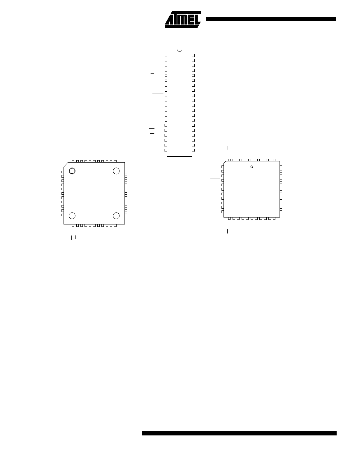
Pin Configurations
1
2
3
4
5
6
7
8
9
10
11
33
32
31
30
29
28
27
26
25
24
23
(MOSI) PB5
(MISO) PB6
(SCK) PB7
RESET
(RXD0) PD0
NC*
(TXD0) PD1
(INT0) PD2
(INT1) PD3
(TOSC1) PD4
(OCIA/TOSC2) PD5
PA4 (AD4)
PA5 (AD5)
PA6 (AD6)
PA7 (AD7)
PE0 (ICP/INT2)
NC*
PE1 (ALE)
PE2 (OC1B)
PC7 (A15)
PC6 (A14)
PC5 (A13)
4443424140393837363534
1213141516171819202122
(WR) PD6
(RD) PD7
XTAL2
XTAL1
GND
NC*
(A8) PC0
(A9) PC1
(A10) PC2
(A11) PC3
(A12) PC4
PB4 (SS)
PB3 (TXD1/AIN1)
PB2 (RXD1/AIN0)
PB1 (OC2/T1)
PB0 (OC0/T0)
NC*
VCC
PA0 (AD0)
PA1 (AD1)
PA2 (AD2)
PA3 (AD3)
* NC = Do not connect
(Can be used in future devices)
PDIP
TQFP
(OC0/T0) PB0
(OC2/T1) PB1
(RXD1/AIN0) PB2
(TXD1/AIN1) PB3
(SS) PB4
(MOSI) PB5
(MISO) PB6
(SCK) PB7
RESET
(RXD0) PD0
(TXD0) PD1
(INT0) PD2
(INT1) PD3
(TOSC1) PD4
(OC1A/TOSC2) PD5
(WR) PD6
(RD) PD7
XTAL2
XTAL1
GND
1
2
3
4
5
6
7
8
9
10
11
12
13
14
15
16
17
18
19
20
40
VCC
39
PA0 (AD0)
38
PA1 (AD1)
37
PA2 (AD2)
36
PA3 (AD3)
35
PA4 (AD4)
34
PA5 (AD5)
33
PA6 (AD6)
32
PA7 (AD7)
31
PE0 (ICP/INT2)
30
PE1 (ALE)
29
PE2 (OC1B)
28
PC7 (A15)
27
PC6 (A14)
26
PC5 (A13)
25
PC4 (A12)
24
PC3 (A11)
23
PC2 (A10)
22
PC1 (A9)
21
PC0 (A8)
(MOSI) PB5
(MISO) PB6
(SCK) PB7
(RXD0) PD0
(TXD0) PD1
(INT0) PD2
(INT1) PD3
(TOSC1) PD4
(OC1A/TOSC2) PD5
RESET
NC*
PLCC
PB4 (SS)
PB3 (TXD1/AIN1)
PB2 (RXD1/AIN0)
PB1 (OC2/T1)
PB0 (OC0/T0)
NC*
VCC
PA0 (AD0)
65432
7
8
9
10
11
12
13
14
15
16
17
1819202122232425262728
(RD) PD7
(WR) PD6
XTAL2
XTAL1
GND
1
NC*
4443424140
(A8) PC0
(A9) PC1
PA1 (AD1)
PA2 (AD2)
PA3 (AD3)
39
PA4 (AD4)
38
PA5 (AD5)
37
PA6 (AD6)
36
PA7 (AD7)
35
PE0 (ICP/INT2)
34
NC*
33
PE1 (ALE)
32
PE2 (OC1B)
31
PC7 (A15)
30
PC6 (A14)
PC5 (A13)
29
* NC = Do not connect
(Can be used in future devices)
(A10) PC2
(A11) PC3
(A12) PC4
Description
The ATmega161 is a low-power CMOS 8-bit microcontroller based on the AVR RISC architec ture. B y execu ting po werful
instructions in a single clock cycl e, the ATme ga161 achi eves throu ghputs ap proach ing 1 MIP S per MHz allo wing the system designer to op timi ze p ower c ons umption ve rsu s pro cessi ng s peed .The A VR
32 general purpose workin g registers. All the 32 registers are directl y connected to the Arithm etic Logic Unit (ALU),
allowing two independent registers to be accessed in one single instruction executed in one clock cycle. The resulting
architecture is more code efficient while achieving throughputs up to ten times faster than conventional CISC
microcontrollers.
The ATmega161 provides the followi ng features: 16K bytes of In-System- or Self-programmable Flash, 512 bytes
EEPROM, 1K bytes SR AM , 35 general purpose I/O l ine s, 32 g ener a l pu rpos e wor king registers, Real Time Cou nter , th re e
flexible timer/counters with compare modes, internal and external interrupts, two programmable serial UARTs, programmable Watchdog Timer with internal oscillator, an SPI serial port and three software selectable power saving modes. The Idle
mode stops the CPU while a llow ing t he S RAM, timer /cou nters, SPI port and interr upt s ystem to c ontin ue fu ncti oning. T he
power-down mode s aves the registe r an d SRA M co ntents but freez es the osci llato r, dis ablin g all othe r ch ip fu nctio ns unti l
the next external interrupt or hardware reset. In Power Save mode, the timer oscillator continues to run, allowing the user to
maintain a timer base while the rest of the device is sleeping.
The device is manufac tured using At mel’s h igh density nonv olati le memor y t echno logy. T he o n-chip Flas h pro gram memory can be reprogrammed using the self-programming capability through the bootblock, using an ISP through the SPI-port,
or by using a conventional nonvolatile memory programmer. By combining an enhanced RISC 8-bit CPU with In-System
Programmable Flash on a monolithic chip, the Atmel ATmega161 is a powerful microcontroller that provides a highly
flexible and cost effective solution to many embedded control applications.
The ATmega161 AVR
macro assemblers, program debugger/simulators, in-circuit emulators, and evaluation kits.
2
core combines a rich instruction set with
is supported with a full suite of program and system development tools including: C compilers,
ATmega161(L)
Page 3
Block Diagram
Figure 1. The ATmega161 Block Diagram
ATmega161(L)
VCC
GND
PORTA DRIVERS
DATA REGISTER
PORTA
PROGRAM
COUNTER
PROGRAM
FLASH
INSTRUCTION
REGISTER
INSTRUCTION
DECODER
PA0-PA7
DATA DIR.
REG. PORTA
STACK
POINTER
SRAM
GENERAL
PURPOSE
REGISTERS
X
Y
Z
DATA REGISTER
8-BIT DATA BUS
PORTC DRIVERS
PORTC
INTERNAL
OSCILLATOR
WATCHDOG
TIMER
MCU CONTROL
REGISTER
TIMER/
COUNTERS
INTERRUPT
UNIT
PC0-PC7
DATA DIR.
REG. PORTC
OSCILLATOR
TIMING AND
CONTROL
XTAL1
XTAL2
RESET
ARATOR
ANALOG
COMP
-
+
CONTROL
LINES
PROGRAMMING
LOGIC
DATA REGISTER
PORTB
STATUS
REGISTER
DATA DIR.
REG. PORTB
PORTB DRIVERS
PB0 - PB7
ALU
SPI
DATA REGISTER
PORTD
PORTD DRIVERS
EEPROM
UARTS
REG. PORTD
PD0 - PD7
DATA DIR.
DATA REG.
PORTE
PORTE DRIVERS
PE0 - PE2
DATA DIR
REG. PORTE
3
Page 4

Pin Descriptions
VCC
Supply voltage
GND
Ground
Port A (PA7..PA0)
Port A is an 8-bit bidirectional I/O port. Port pins can provide internal pull-up resistors (selected for each bit). The Port A
output buffers ca n sink 20 mA and c an drive LED disp lays dir ectly. When pi ns PA0 to PA7 ar e used as inputs and are
externally pulled low, they will source current if the internal pull- up resistors are activated. The Port A pins are tri-stated
when a reset condition becomes active, even if the clock is not running.
Port A serves as Multiplexed Address/Data port when using external memory interface.
Port B (PB7..PB0)
Port B is an 8 -bit bi dir ectional I/O por t with inte rnal pu ll- up res istors . The Port B o utput buffer s can sink 20 mA. As inp uts,
Port B pins that are externally pulled low will source current if the pull-up resistors are activated. The Port B pins are
tri-stated when a reset condition becomes active, even if the clock is not running.
Port B also serves the functions of various special features of the ATmega161 as listed on page 80.
Port C (PC7..PC0)
Port C is an 8-bit bidire ctiona l I/O po rt wit h inter nal pull-up resi stors. The Port C ou tpu t buffers can si nk 20 mA. A s inputs ,
Port C pins that are externally pulled low will source current if the pull-up resistors are activated. The Port C pins are
tri-stated when a reset condition becomes active, even if the clock is not running.
Port C also serves as Address high output when using external memory interface.
Port D (PD7..PD0)
Port D is an 8-bit bidire ctiona l I/O po rt wit h inter nal pull-up resi stors. The Port D ou tpu t buffers can si nk 20 mA. A s inputs ,
Port D pins that are externally pulled low will source current if the pull-up resistors are activated. The Port D pins are
tri-stated when a reset condition becomes active, even if the clock is not running.
Port D also serves the functions of various special features of the ATmega161 as listed on page 87.
Port E (PE2..PE0)
Port E is a 3-bit bidirectional I/O port with internal pull-up resistors. The Port E output buffers can sink 20 mA. As inputs,
Port E pins that are externally pulled low will source current if the pull-up resistors are activated. The Port E pins are
tri-stated when a reset condition becomes active, even if the clock is not running.
Port E also serves the functions of various special features of the ATmega161 as listed on page 93.
RESET
Reset input. A low level on thi s pin for more than 500 ns will generate a res et, even if the clock i s not running. Sho rter
pulses are not guaranteed to generate a reset.
XTAL1
Input to the inverting oscillator amplifier and input to the internal clock operating circuit.
XTAL2
Output from the inverting oscillator amplifier
4
ATmega161(L)
Page 5
ATmega161(L)
Crystal Oscillator
XTAL1 and XTAL2 are input and output, respectively, of an inverting amplifier which can be configured for use as an
on-chip oscillator, as shown in Figure 2. Either a quartz crystal or a ceramic resonator may be used. To drive the device
from an external clock source, XTAL2 should be left unconnected while XTAL1 is driven as shown in Figure 3.
Figure 2. Oscillator Connections
MAX 1 HC BUFFER
HC
C2
C1
Note: When using the MCU Oscillator as a clock for an external device, an HC buffer should be connected as indicated in the figure.
Figure 3. External Clock Drive Configuration
XTAL2
XTAL1
GND
5
Page 6
Architectural Overview
The fast-access register file concept contains 32 x 8-bit general purpose working registers with a single clock cycle access
time. This means th at d urin g on e s in gl e cloc k cyc le, one Arithmetic Logic Uni t ( ALU) op er ation i s ex ecute d. T wo ope ra nds
are output from the register file, the operation is executed, and the result is stored back in the register file – in one clock
cycle.
Six of the 32 registers can be used as three 16-bits indirect address register pointers for Data Space addressing – enabling
efficient address cal cula tions. One of the three addre ss po inters i s also used a s the ad dres s pointer for the const ant tabl e
look up function. These added function registers are the 16-bits X-register, Y-register and Z-register.
Figure 4. The ATmega161 AVR
RISC Architecture
AVR
8K x 16
Program
Memory
Instruction
Register
Instruction
Decoder
Control Lines
ATmega161 Architecture
Program
Counter
Direct Addressing
Indirect Addressing
Data Bus 8-bit
Status
and Control
32 x 8
General
Purpose
Registers
ALU
1024 x 8
Data
SRAM
Interrupt
Unit
SPI
Unit
Serial
UART0
Serial
UART1
8-bit
Timer/Counter
with PWM
and RTC
16-bit
Timer/Counter
with PWM
8-bit
Timer/Counter
with PWM
512 x 8
EEPROM
32
I/O Lines
6
ATmega161(L)
Watchdog
Timer
Analog
Comparator
Page 7

ATmega161(L)
The ALU supports arithmetic and logic functions between registers or between a constant and a register. Single register
operations are also executed in the ALU. Figure 4 shows the ATmega161 AVR
RISC microcontroller architecture.
In addition to the register operation, the conventional memory addressing modes can be used on the register file as well.
This is enabled by the fa ct th at the re giste r file is assig ned t he 32 lowe rmost Dat a Spa ce add resses ( $00 - $ 1F), allo wing
them to be accessed as though they were ordinary memory locations.
The I/O memory spac e contai ns 64 a ddresses for CPU peripheral function s as Contr ol Regis ters, Tim er/Counters , and
other I/O functions. The I/O M emo ry c an be a cc ess ed d ir ectly , o r a s the D ata S pa ce loc at ion s f oll owing thos e o f the register file, $20 - $5F.
The AVR
uses a Harvard architecture concept – with separate memories and buses for program and data. The program
memory is executed with a two stage pipeline. While one instruction is being executed, the next instruction is pre-fetched
from the program memory. This conc ept enable s instru ctio ns to be executed in every cl ock cyc le. The program memory is
Self-programmable Flash memory.
With the jump and call in struc tions , the whol e 8K word ad dress sp ace is directl y acce ssed. Mo st AVR
instructio ns hav e a
single 16-bit word format. Every program memory address contains a 16- or 32-bit instruction.
During interrupts and su broutine call s, the r etur n addres s pr ogram co unte r (PC) is stored on the sta ck. The stac k is effe c-
tively allocate d in the ge neral data SR AM, an d consequen tly the st ack size is only limi ted by the total SRAM size and th e
usage of the SRAM. All us er progra ms must initialize the S P (Stack P ointer) in the res et routin e (befor e subroutin es or
interrupts are executed). The 16-bit stack pointer is read/write accessible in the I/O space.
The 1K bytes data SRAM can be easi ly accessed through the five different addressing modes s upported in the AVR
architecture.
The memory spaces in the AVR
architecture are all linear and regular memory maps.
7
Page 8
Figure 5. Memory Maps
Program Memory
Data Memory
Program Flash
(8K x 16)
$000
$1FFF
32 Gen. Purpose
Working Registers
64 I/O Registers
Internal SRAM
(1024 x 8)
External SRAM
(0-63K x 8)
$0000
$001F
$0020
$005F
$0060
$045F
$0460
$FFFF
A flexible interrupt module has its control registers in the I/O space with an additional global interrupt enable bit in the status
register. All the different interrupts have a separate interrupt vector in the interrupt vector table at the beginning of the
program me mory. The di fferen t interr upts hav e prior ity in acco rdance with th eir inte rrupt v ector p ositi on. The lower the
interrupt vector address, the higher the priority.
8
ATmega161(L)
Page 9
General Purpose Register File
Figure 6 shows the structure of the 32 general purpose working registers in the CPU.
Figure 6. AVR
CPU General Purpose Working Registers
70Addr.
R0 $00
R1 $01
R2 $02
…
R13 $0D
General R14 $0E
Purpose R15 $0F
Working R16 $10
Registers R17 $11
…
R26 $1A X-register low byte
R27 $1B X-register high byte
R28 $1C Y-register low byte
R29 $1D Y-register high byte
R30 $1E Z-register low byte
R31 $1F Z-register high byte
ATmega161(L)
All the register operat ing instructi ons in the instruction s et have dir ect and s ingle cycle acc ess to all r egisters. T he only
exceptions are the five constant arithmetic and logic instructions SBCI, SUBI, CPI, ANDI, and ORI between a constant and
a register, and the LDI ins truc ti on for l oad i mm edi ate c on stant da ta. T he se instr uct io ns appl y to the secon d hal f of th e r egisters in the regis ter file – R1 6..R31 . The gen eral SB C, SUB, CP, AN D, and OR, a nd all ot her op erations between two
registers or on a single register apply to the entire register file.
As shown in Figu re 6, each regi ster is als o as signe d a da ta mem ory add ress , map ping t hem direct ly i nto the first 32 loc ations of the user Data Space. Although not being physicall y implemented as SRAM locati ons, this memory organiza tion
provides great flexibility in access of the registers, as the X, Y and Z-registers can be set to index any register in the file.
X-register, Y-register, and Z-register
The registers R2 6..R31 have som e add ed fun ction s to their gener al p urpose usa ge. The se r egister s are addr ess p ointe rs
for indirect addressing of the Data Space. The three indirect address registers X, Y and Z are defined as:
Figure 7. X, Y and Z-registers
15 0
X-register 7 0 7 0
R27 ($1B) R26 ($1A)
15 0
Y-register 7 0 7 0
R29 ($1D) R28 ($1C)
15 0
Z-register 7 0 7 0
R31 ($1F) R30 ($1E)
In the different address ing mod es , thes e ad dres s r egi ster s h ave func ti ons as f ixed di s pla ce men t, aut oma tic inc r em ent an d
decrement (see the descriptions for the different instructions).
9
Page 10
ALU – Arithmetic Logic Unit
The high-performance AVR ALU operates in direct connection with all the 32 general purpose working registers. Within a
single clock cy cl e, AL U ope r atio ns be tween r egi ster s in the re gis te r f ile ar e ex ec uted . The ALU operations are div i ded in to
three main catego ries – arithmetic, logica l, an d bit- func tions. A Tme ga161 does also p rovide a po werful mul tipli er sup porting both signed/unsigned multiplication and fractional format. See Instruction Set section for a detailed description.
Self-programmable Flash Program Memory
The ATmega161 contains 16K bytes on-chip Self- and In-System programmable Flash memory for program storage. Since
all instructions a re 16- or 32 -bit words, the Flash is or ga nized as 8K x 16. The Flas h me mory has an end ur ance of at least
1000 write/erase cycles. The ATmega161 Program Counter ( PC) is 13 bi ts wide, thus addressing the 819 2 program
memory locations.
See page 95 for a detailed description on Flash data downloading.
See page 11 for the different program memory addressing modes.
EEPROM Data Memory
The ATmega161 contains 512 bytes of data EEPROM memory. It is organized as a separate data space, in which single
bytes can be read and written. The EEPROM has an endurance of at least 100,000 write/erase cycles per location. The
interface between the EEPROM and the CPU is described on page 54 specifying the EEPROM address registers, the
EEPROM data register, and the EEPROM control register.
For the SPI data downloading, see page 109 for a detailed description.
Figure 8. SRAM Organization
Register File Data Address Space
R0 $0000
R1 $0001
R2 $0002
º º
R29 $001D
R30 $001E
R31 $001F
I/O Registers
$00 $0020
$01 $0021
$02 $0022
……
$3D $005D
$3E $005E
$3F $005F
Internal SRAM
$0060
$0061
º
$045E
$045F
10
ATmega161(L)
Page 11

ATmega161(L)
SRAM Data Memory
Figure 8 shows how the ATmega161 SRAM Memory is organized.
The lower 1120 Data Memory locations address the Register file, the I/O Memory and the internal data SRAM. The first 96
locations address the Register File and I/O Memory, and the next 1K loc ations address the internal data SRAM. An
optional external data memory device can be placed in the same SRAM memory space. This memory device will occupy
the locations following the internal SRAM and up to as much as 64K - 1, depending on external memory size.
When the addresses acc essing the da ta memory sp ace exc eeds the int ernal data SRA M locati ons, the memor y device is
accessed using the same instructions as for the internal data SRAM access. When the internal data space is accessed, the
read and write strobe pins (RD
by setting the SRE bit in the MCUCR register. See “Interface to external memory” on page 72 for details.
Accessing external memory takes one additional clock cycle per byte compared to access of the internal SRAM. This
means that the commands LD, ST, LDS, STS, PUSH and PO P take one a dditional clock cycle. If the s tack is plac ed in
external memory, interr upts, subroutine call s and returns take two clock c ycles extra because the two-by te program
counter is pushed and popped. When external memory interface is used with wait state, two additional clock cycles is used
per byte. This ha s t he foll owin g effe ct : Dat a tr an sfe r in struc ti ons ta ke two ex tra c lo ck c y cl es, whereas interrupt, subr ou tin e
calls and returns will need four clock cycles more than specified in the instruction set manual.
The five different addressing modes for the data memory cover: Direct, Indirect with Displacement, Indirect, Indirect with
Pre-Decrement, and Indire ct with Pos t-Incre ment. In th e regist er file, regi sters R2 6 to R31 feat ure the indi rect add ressing
pointer registers.
The direct addressing reaches the entire data space.
The Indirect with Displacement mode features a 63 address locations reach from the base address given by the Y or
Z-register.
When using register indirect addressing modes with automatic pre-decrement and post-increment, the address registers X,
Y and Z are decremented and incremented.
The 32 general purpose wo rk in g regi st er s, 6 4 I/O regi ste rs an d the 1K bytes of internal data SRA M in the A T meg a161 ar e
all accessible through all these addressing modes.
See the next section for a detailed description of the different addressing modes.
and WR) are inactive during the whole access cycle. External memory operation is enabled
Program and Data Addressing Modes
The ATmega161 AVR RISC microcontroller supports powerful and efficient addressing modes for access to the program
memory (Flash) and data mem or y (SRA M, Regis ter F ile , and I/O Mem or y). T his se cti on de scr ibe s the diffe re nt add ress in g
modes supported by the AVR
simplify, not all figures show the exact location of the addressing bits.
architecture. In the figures, OP means the operation code part of the instruction word. T o
11
Page 12
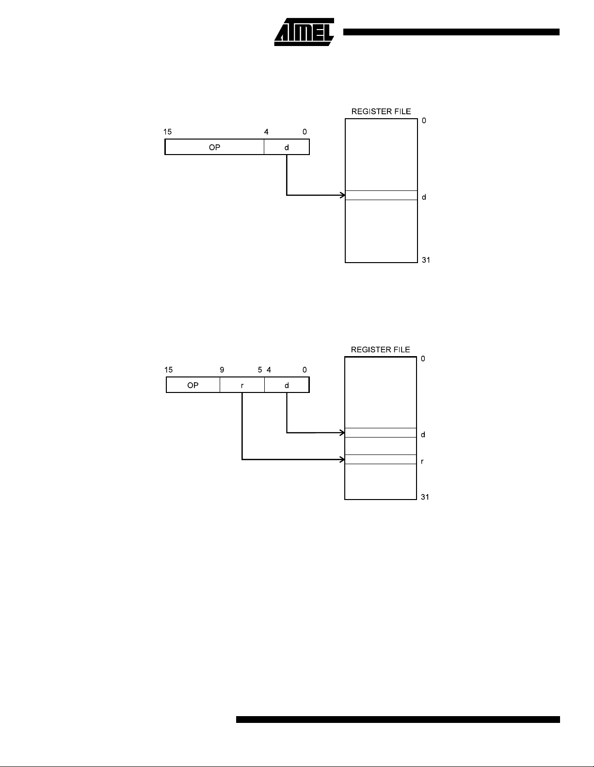
Register Direct, Single Register Rd
Figure 9. Direct Single Register Addressing
The operand is contained in register d (Rd).
Register Direct, Two Registers Rd and Rr
Figure 10. Direct Register Addressing, Two Registers
Operands are contained in register r (Rr) and d (Rd). The result is stored in register d (Rd).
12
ATmega161(L)
Page 13
ATmega161(L)
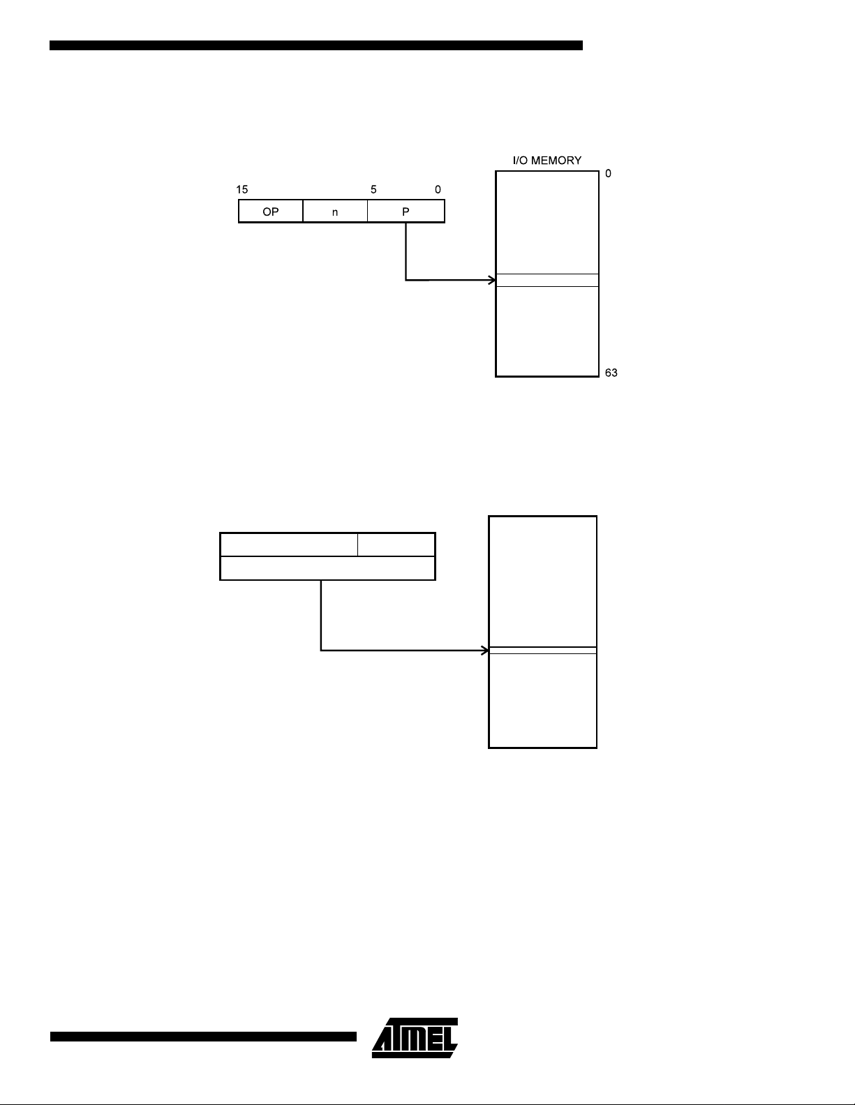
I/O Direct
Figure 11. I/O Direct Addressing
Operand address is contained in 6 bits of the instruction word. n is the destination or source register address.
Data Direct
Figure 12. Direct Data Addressing
Data Space
$0000
$FFFF
16 LSBs
20 19
16
31
OP Rr/Rd
15 0
A 16-bit Data Address is contained in the 1 6 LSBs of a two-word instructio n. Rd/Rr specify the destination or sourc e
register.
13
Page 14
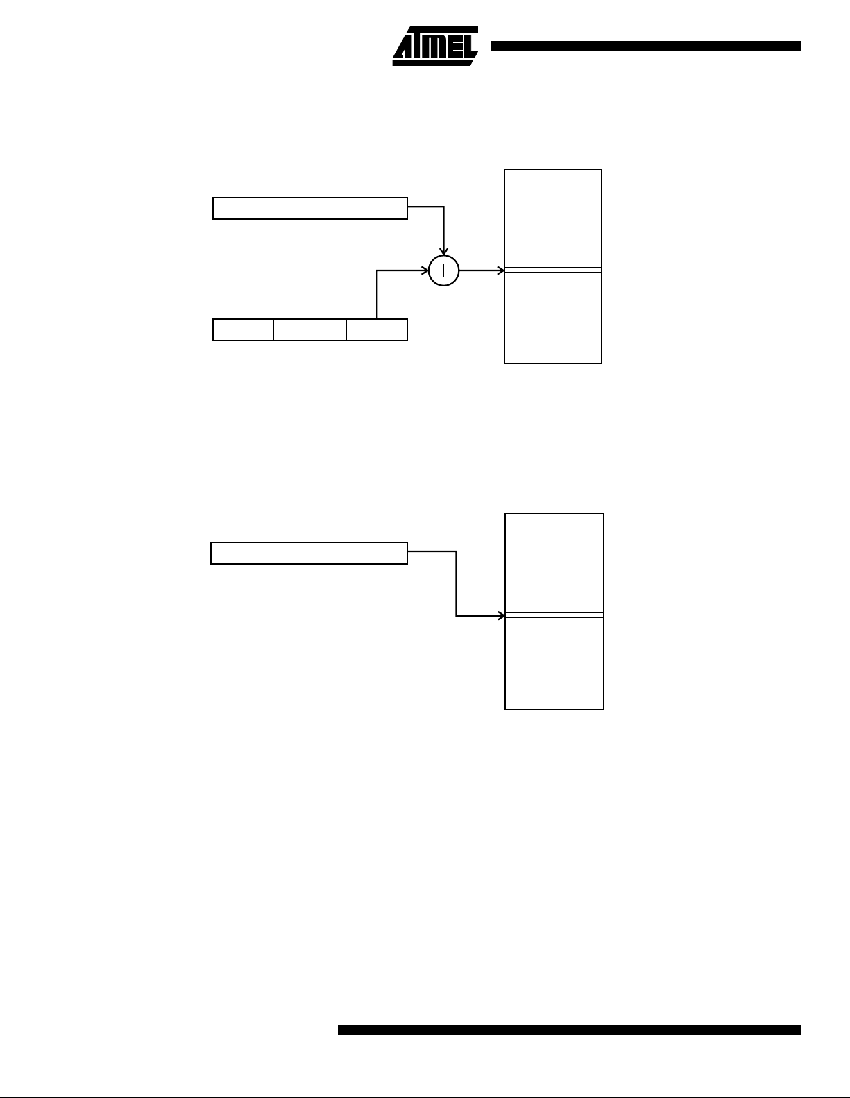
Data Indirect with Displacement Figure 13. Data Indirect with Displacement
15
Y OR Z - REGISTER
Data Space
$0000
0
15
OP an
05610
$FFFF
Operand address is the result of the Y or Z-register contents added to the address contained in 6 bits of the
instruction word.
Data Indirect
Figure 14. Data Indirect Addressing
Data Space
015
X, Y, OR Z - REGISTER
$0000
$FFFF
Operand address is the contents of the X, Y, or the Z-register.
14
ATmega161(L)
Page 15
ATmega161(L)
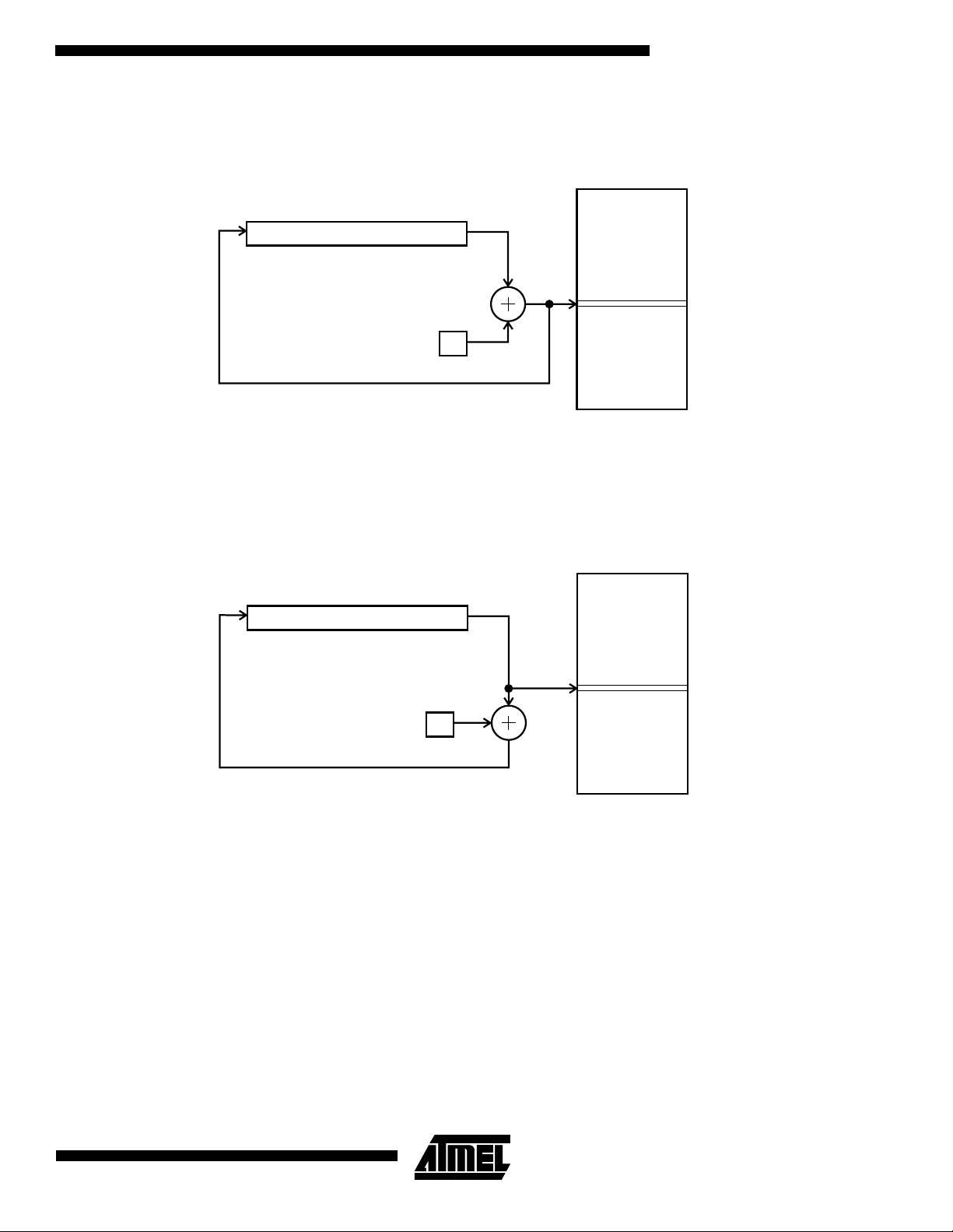
Data Indirect with Pre-Decrement
Figure 15. Data Indirect Addressing with Pre-Decrement
Data Space
015
X, Y, OR Z - REGISTER
-1
The X, Y, or the Z-register is decremented before the operation. Operand address is the decremented contents of the X, Y,
or the Z-register.
$0000
$FFFF
Data Indirect with Post-Increment
Figure 16. Data Indirect Addressing with Post-Increment
Data Space
015
X, Y, OR Z - REGISTER
1
$0000
$FFFF
The X, Y, or the Z-register is inc r em ente d afte r th e ope ratio n. O per an d add ress is the con tent of the X , Y, o r th e Z-re g ister
prior to incrementing.
15
Page 16

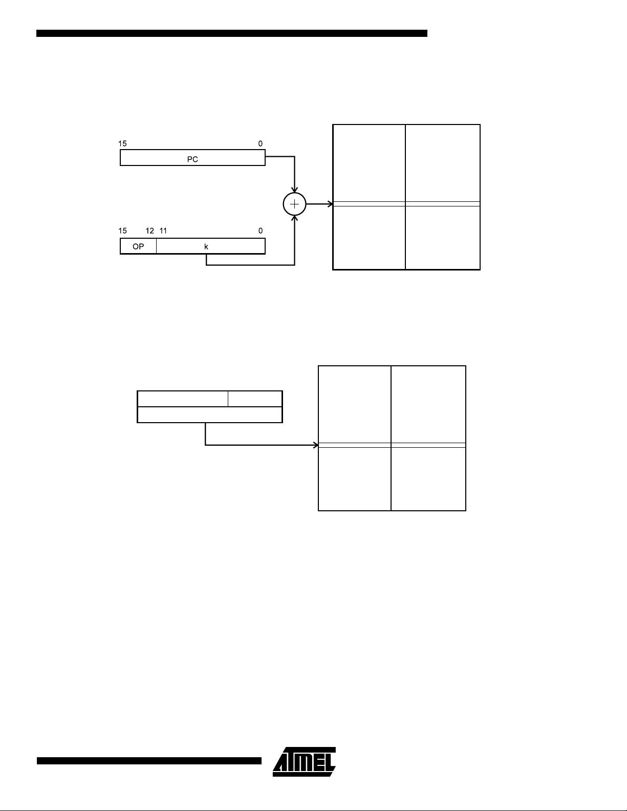
Constant Addressing Using the LPM Instruction
Figure 17. Code Memory Constant Addressing
PROGRAM MEMORY
$000
$1FFF
Constant byte addr ess is s pe cif ie d b y the Z-r eg ister c on tents. The 15 MSBs se le ct wor d add re ss ( 0 - 8K ), the LS B se le cts
low byte if cleared (LSB = 0) or high byte if set (LSB = 1).
Indirect Program Addressing, IJMP and ICALL
Figure 18. Indirect Program Memory Addressing
PROGRAM MEMORY
$000
$1FFF
Program execution continues at address contained by the Z-register (i.e. the PC is loaded with the contents of the
Z-register).
16
ATmega161(L)
Page 17
ATmega161(L)
Relative Program Addressing, RJMP and RCALL
Figure 19. Relative Program Memory Addressing
PROGRAM MEMORY
Program execution continues at address PC + k + 1. The relative address k is -2048 to 2047.
Direct Program Addressing, JMP and CALL
$000
$1FFF
Figure 20. Direct Program Addressing
PROGRAM MEMORY
31
OP
15 0
21 20
16 LSBs
16
Program execution continues at the address immediate in the instruction words.
$0000
$1FFF
17
Page 18
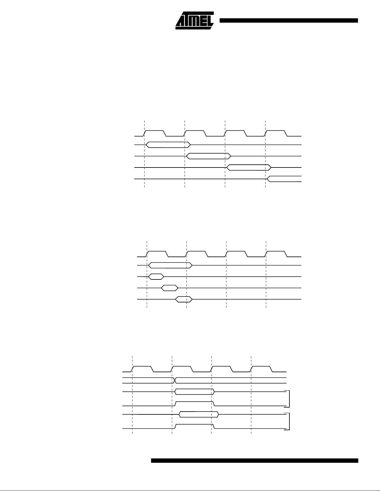
Memory Access Times and Instruction Execution Timing
This section describes the general access timing concepts for instruction execution and internal memory access.
The AVR
clock division is used.
Figure 21 shows the parallel instruction fetches and instructio n executions enabled by the Harvard architecture and the
fast-access register file concept. This is the basic pipelining concept to obtain up to 1 MIPS per MHz with the corresponding
unique results for functions per cost, functions per clocks, and functions per power-unit.
Figure 21. The Parallel Instruction Fetches and Instruction Executions
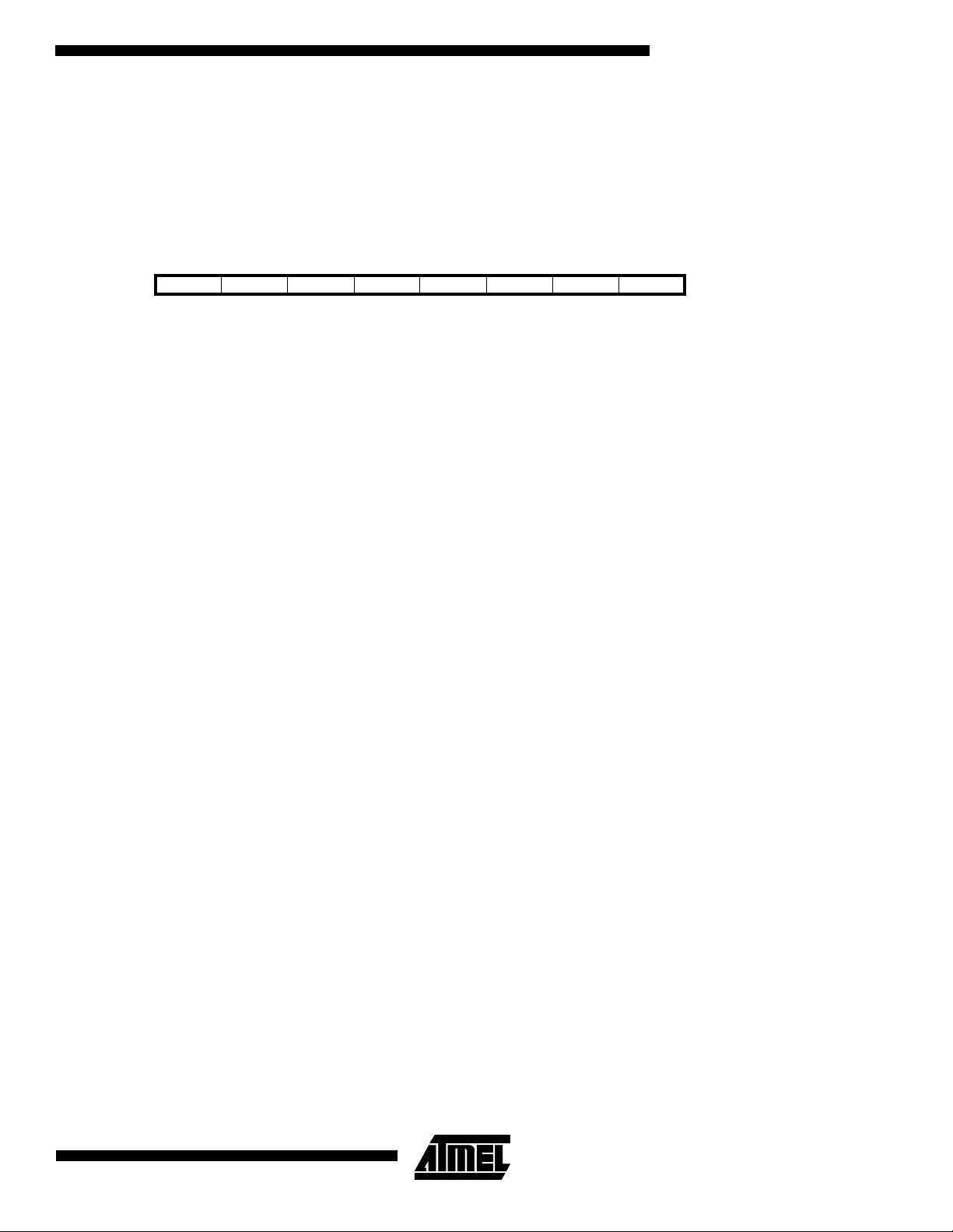
Figure 22 shows the internal timing concept for the register file. In a single clock cycle an ALU operation using two register
operands is executed, and the result is stored back to the destination register.
CPU is driven by the System Clock Ø, directly generated from the external clock crys tal for the chip. No in ternal
T1 T2 T3 T4
System Clock Ø
1st Instruction Fetch
1st Instruction Execute
2nd Instruction Fetch
2nd Instruction Execute
3rd Instruction Fetch
3rd Instruction Execute
4th Instruction Fetch
Figure 22. Single Cycle ALU Operation
T1 T2 T3 T4
System Clock Ø
Total Execution Time
Register Operands Fetch
ALU Operation Execute
Result Write Back
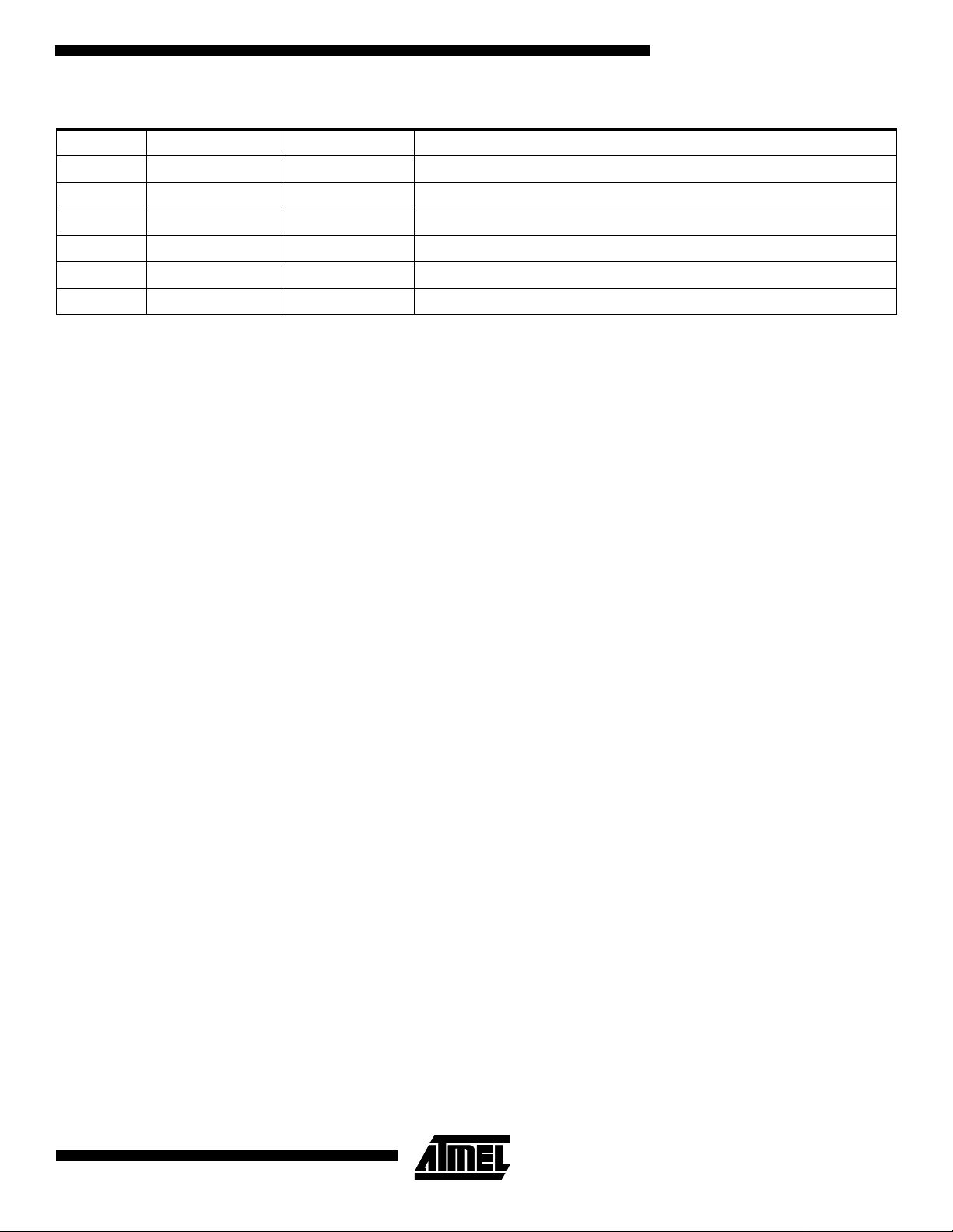
The internal data SRAM access is performed in two System Clock cycles as described in Figure 23.
Figure 23. On-chip Data SRAM Access Cycles
T1 T2 T3 T4
System Clock Ø
Address
Data
WR
Prev. Address
Address
Write
18
Data
RD
ATmega161(L)
Read
Page 19

I/O Memory
The I/O space definition of the ATmega161 is shown in the following table:
Table 1. ATmega161 I/O Space
I/O Address (SRAM Address) Name Function
$3F($5F) SREG Status REGister
$3E ($5E) SPH Stack Pointer High
$3D ($5D) SPL Stack Pointer Low
$3B ($5B) GIMSK General Interrupt MaSK register
$3A ($5A) GIFR General Interrupt Flag Register
$39 ($59) TIMSK Timer/Counter Interrupt MaSK Register
$38 ($58) TIFR Timer/Counter Interrupt Flag Register
$37 ($57) SPMCR Store Program Memory Control Register
$36 ($56) EMCUCR Extended MCU general Control Register
$35 ($55) MCUCR MCU general Control Register
$34 ($54) MCUSR MCU general Status Register
ATmega161(L)
$33 ($53) TCCR0 Timer/Counter0 Control Register
$32 ($52) TCNT0 Timer/Counter0 (8-bit)
$31 ($51) OCR0 Timer/Counter0 Output Compare Register
$30 ($50) SFIOR Special Function IO Register
$2F ($4F) TCCR1A Timer/Counter1 Control Register A
$2E ($4E) TCCR1B Timer/Counter1 Control Register B
$2D ($4D) TCNT1H Timer/Counter1 High Byte
$2C ($4C) TCNT1L Timer/Counter1 Low Byte
$2B ($4B) OCR1AH Timer/Counter1 Output Compare RegisterA High Byte
$2A ($4A) OCR1AL Timer/Counter1 Output Compare RegisterA Low Byte
$29 ($49) OCR1BH Timer/Counter1 Output Compare RegisterB High Byte
$28 ($48) OCR1BL Timer/Counter1 Output Compare RegisterB Low Byte
$27 ($47) TCCR2 Timer/Counter2 Control Register
$26 ($46) ASSR Asynchronous mode StatuS Register
$25 ($45) ICR1H Timer/Counter1 Input Capture Register High Byte
$24 ($44) ICR1L Timer/Counter1 Input Capture Register Low Byte
$23 ($43) TCNT2 Timer/Counter2 (8-bit)
$22 ($42) OCR2 Timer/Counter2 Output Compare Register
$21 ($41) WDTCR Watchdog Timer Control Register
$20 ($40) UBRRHI UART Baud Register HIgh
$1F ($3F) EEARH EEPROM Address Register High
$1E ($3E) EEARL EEPROM Address Register Low
$1D ($3D) EEDR EEPROM Data Register
19
Page 20

Table 1. ATmega161 I/O Space (Continued)
I/O Address (SRAM Address) Name Function
$1C ($3C) EECR EEPROM Control Register
$1B($3B) PORTA Data Register, Port A
$1A ($3A) DDRA Data Direction Register, Port A
$19 ($39) PINA Input Pins, Port A
$18 ($38) PORTB Data Register, Port B
$17 ($37) DDRB Data Direction Register, Port B
$16 ($36) PINB Input Pins, Port B
$15 ($35) PORTC Data Register, Port C
$14 ($34) DDRC Data Direction Register, Port C
$13 ($33) PINC Input Pins, Port C
$12 ($32) PORTD Data Register, Port D
$11 ($31) DDRD Data Direction Register, Port D
$10 ($30) PIND Input Pins, Port D
$0F ($2F) SPDR SPI I/O Data Register
$0E ($2E) SPSR SPI Status Register
$0D ($2D) SPCR SPI Control Register
$0C ($2C) UDR0 UART0 I/O Data Register
$0B ($2B) UCSR0A UART0 Control and Status Register
$0A ($2A) UCSR0B UART0 Control and Status Register
$09 ($29) UBRR0 UART0 Baud Rate Register
$08 ($28) ACSR Analog Comparator Control and Status Register
$07 ($27) PORTE Data Register, Port E
$06 ($26) DDRE Data Direction Register, Port E
$05 ($25) PINE Input Pins, Port E
$03 ($23) UDR1 UART1 I/O Data Register
$02 ($22) UCSR1A UART1 Control and Status Register
$01 ($21) UCSR1B UART1 Control and Status Register
$00 ($20) UBRR1 UART1 Baud Rate Register
Note: Reserved and unused locations are not shown in the table.
All ATmega161 I/Os and peripherals are placed in the I/O space. The I/O locations are accessed by the IN and OUT
instructions transfer ring data be tween the 32 gen eral purpose wor king regis ters an d the I/O space . I/O regist ers wit hin the
address range $00 - $1F are directl y bit-acces sible us ing the SBI and CBI instruct ions. In these re giste rs, the value of single bits can be check ed by using the SBIS and SB IC instructi ons. Refer to th e instructi on set chap ter for more details.
When using the I/O specific commands IN, OUT the I/O addresses $00 - $3F must be used. When addressing I/O registers
as SRAM, $20 must be added to this address. All I/O regi ster addresses throughout this document are shown with the
SRAM address in parentheses.
For compatibilit y with fut ur e d evi ce s, r es erve d b its s hou ld be wr itte n t o z er o if a cces s ed. Rese rve d I/ O mem or y addresses
should never be written.
20
ATmega161(L)
Page 21
ATmega161(L)
Some of the status flags are cleared by writing a logical one to them. Note that the CBI and SBI instructions will operate on
all bits in the I/O regi ster , writing a on e back in to an y flag r ead as set, th us clea ring t he flag . The C BI and SB I instr ucti ons
work with registers $00 to $1F only.
The I/O and peripherals control registers are explained in the following sections.
Status Register – SREG
The AVR status register – SREG – at I/O space location $3F ($5F) is defined as:
Bit 76543210
$3F ($5F) I T H S V N Z C SREG
Read/Write R/W R/W R/W R/W R/W R/W R/W R/W
Initial value 0 0 0 0 0 0 0 0
Bit 7 - I: Global Interrupt Enable
•
The global interrup t enable bit must be set (one) for the interrup ts to be enable d. The indivi dual inter rupt enab le control is
then performed in separate control registers. If the global interrupt enable bit is cleared (zero), none of the interrupts are
enabled independent of the individual interrupt enable settings. The I-bit is cleared by hardware after an interrupt has
occurred, and is set by the RETI instruction to enable subsequent interrupts.
Bit 6 - T: Bit Copy Storage
•
The bit copy instructions BLD (Bit LoaD) and BST (Bit STore) use the T bit as source and destination for the operated bit. A
bit from a register in the regi ste r fi le can be copi ed i nto T by the B ST i ns tru ct ion , and a bit i n T can be c opied i nto a bit i n a
register in the register file by the BLD instruction.
Bit 5 - H: Half Carry Flag
•
The half carry flag H indicates a half carry in some arithmetic operations. See the Instruction Set Description for detailed
information.
Bit 4 - S: Sign Bit, S = N ⊕ V
•
The S-bit is always an exclusive or between the negative flag N and the two’s complement overflow flag V. See the Instruction Set Description for detailed information.
•
Bit 3 - V: Two’s Complement Overflow Flag
The two’s comp lement overflow flag V s upports two’s complement arithmetics. See the Instruction Set Description for
detailed information.
Bit 2 - N: Negative Flag
•
The negative flag N indicates a negative result after the different arithmetic and logic operations. See the Instruction Set
Description for detailed information.
Bit 1 - Z: Zero Flag
•
The zero flag Z indicates a zero result after the different arithmetic and logic operations. See the Instruction Set Description
for detailed information.
•
Bit 0 - C: Carry Flag
The carry flag C indicates a c arry in an arithmetic or logic operation. S ee the Instruction S et Description for detail ed
information.
Note that the status register is not automatically stored when entering an interrupt routine and restored when returning from
an interrupt routine. This must be handled by software.
21
Page 22

Stack Pointer – SP
The ATmega161 Stac k Point er is impl emented as two 8-bit r egist ers in th e I/O sp ace lo ca tions $3E ($5E ) and $3D ($5D) .
As the ATmega161 supports up to 64KB memory, all 16 bits are used.
Bit 151413121110 9 8
$3E ($5E) SP15 SP14 SP13 SP12 SP11 SP10 SP9 SP8 SPH
$3D ($5D) SP7 SP6 SP5 SP4 SP3 SP2 SP1 SP0 SPL
76543210
Read/Write R/W R/W R/W R/W R/W R/W R/W R/W
R/W R/W R/W R/W R/W R/W R/W R/W
Initial value 0 0 0 0 0 0 0 0
00000000
The Stack Poin ter po ints to th e da ta SRA M s tack area whe re the Subr outi ne an d Inte rru pt St acks are loca ted. T his Sta ck
space in the d ata SRAM m ust be defi ned by the program before any subroutine calls ar e executed or interrupts are
enabled. The stack pointer must be set to point above $60. The Stack Pointer is decremented by one when data is pushed
onto the Stack with the PUSH instruction, and it is decremented by two when an address is pushed onto the Stack with
subroutine calls and interrupts. The Stack Pointer is incremented by one when data is popped from the Stack with the POP
instruction, and it is incremen ted by two when an addres s is popped from the Stack with return from subroutine RET or
return from interrupt RETI.
Reset and Interrupt Handling
The ATmega161 pr ovide s 20 d iff er ent int er rupt s ou rces . T h es e in terr up ts and the se par at e r ese t ve cto r, each hav e a s eparate program vector in the program memory space. All interrupts are assigned individual enable bits which must be set
(one) together with the I-bit in the status register in order to enable the interrupt.
The lowest addresses i n the pro gram memo ry space are automatica lly defined a s the Rese t and Inter rupt vector s. The
complete list of vectors is shown in Table 2. The list also determines the priority levels of the different interrupts. The lower
the address the higher is the priority level. RESET has the highest priority , and next is INT0 – the External Interrupt
Request 0 etc.
Table 2. Reset and Interrupt Vectors
Vector No. Program Address Source Interrupt Definition
1 $000 RESET External Pin, Power-on Reset, Brown-out Reset and Watchd og Re se t
2 $002 INT0 External Interrupt Request 0
3 $004 INT1 External Interrupt Request 1
4 $006 INT2 External Interrupt Request 2
5 $008 TIMER2 COMP Timer/Counter2 Compare Match
6 $00a TIMER2 OVF Timer/Counter2 Overflow
7 $00c TIMER1 CAPT Timer/Counter1 Capture Event
8 $00e TIMER1 COMPA Timer/Counter1 Compare Match A
9 $010 TIMER1 COMPB Timer/Counter1 Compare Match B
10 $012 TIMER1 OVF Timer/Counter1 Overflow
11 $014 TIMER0 COMP Timer/Counter0 Compare Match
12 $016 TIMER0 OVF Timer/Counter0 Overflow
13 $018 SPI, STC Serial Transfer Complete
14 $01a UART0, RX UART0, Rx Complete
15 $01c UART1, RX UART1, Rx Complete
22
ATmega161(L)
Page 23
ATmega161(L)
Table 2. Reset and Interrupt Vectors (Continued)
Vector No. Program Address Source Interrupt Definition
16 $01e UART0, UDRE UART0 Data Register Empty
17 $020 UART1, UDRE UART1 Data Register Empty
18 $022 UART0, TX UART0, Tx Complete
19 $024 UART1, TX UART1, Tx Complete
20 $026 EE_RDY EEPROM Ready
21 $028 ANA_COMP Analog Comparator
The most typical and general program setup for the Reset and Interrupt Vector Addresses are:
Address Labels Code Comments
$000 jmp RESET ; Reset Handler
$002 jmp EXT_INT0 ; IRQ0 Handler
$004 jmp EXT_INT1 ; IRQ1 Handler
$006 jmp EXT_INT2 ; IRQ2 Handler
$008 jmp TIM2_COMP ; Timer2 Compare Handler
$00a jmp TIM2_OVF ; Timer2 Overflow Handler
$00c jmp TIM1_CAPT ; Timer1 Capture Handler
$00e jmp TIM1_COMPA ; Timer1 CompareA Handler
$010 jmp TIM1_COMPB ; Timer1 CompareB Handler
$012 jmp TIM1_OVF ; Timer1 Overflow Handler
$014 jmp TIM0_COMP ; Timer0 Compare Handler
$016 jmp TIM0_OVF ; Timer0 Overflow Handler
$018 jmp SPI_STC; ; SPI Transfer Complete Handler
$01a jmp UART_RXC0 ; UART0 RX Complete Handler
$01c jmp UART_RXC1 ; UART1 RX Complete Handler
$01e jmp UART_DRE0 ; UDR0 Empty Handler
$020 jmp UART_DRE1 ; UDR1 Empty Handler
$022 jmp UART_TXC0 ; UART0 TX Complete Handler
$024 jmp UART_TXC1 ; UART1 TX Complete Handler
$026 jmp EE_RDY ; EEPROM Ready Handler
$028 jmp ANA_COMP ; Analog Comparator Handler
;
$02a MAIN: ldi r16,high(RAMEND); Main program start
$02b out SPH,r16
$02c ldi r16,low(RAMEND)
$02d out SPL,r16
$02e <instr> xxx
… … … …
23
Page 24
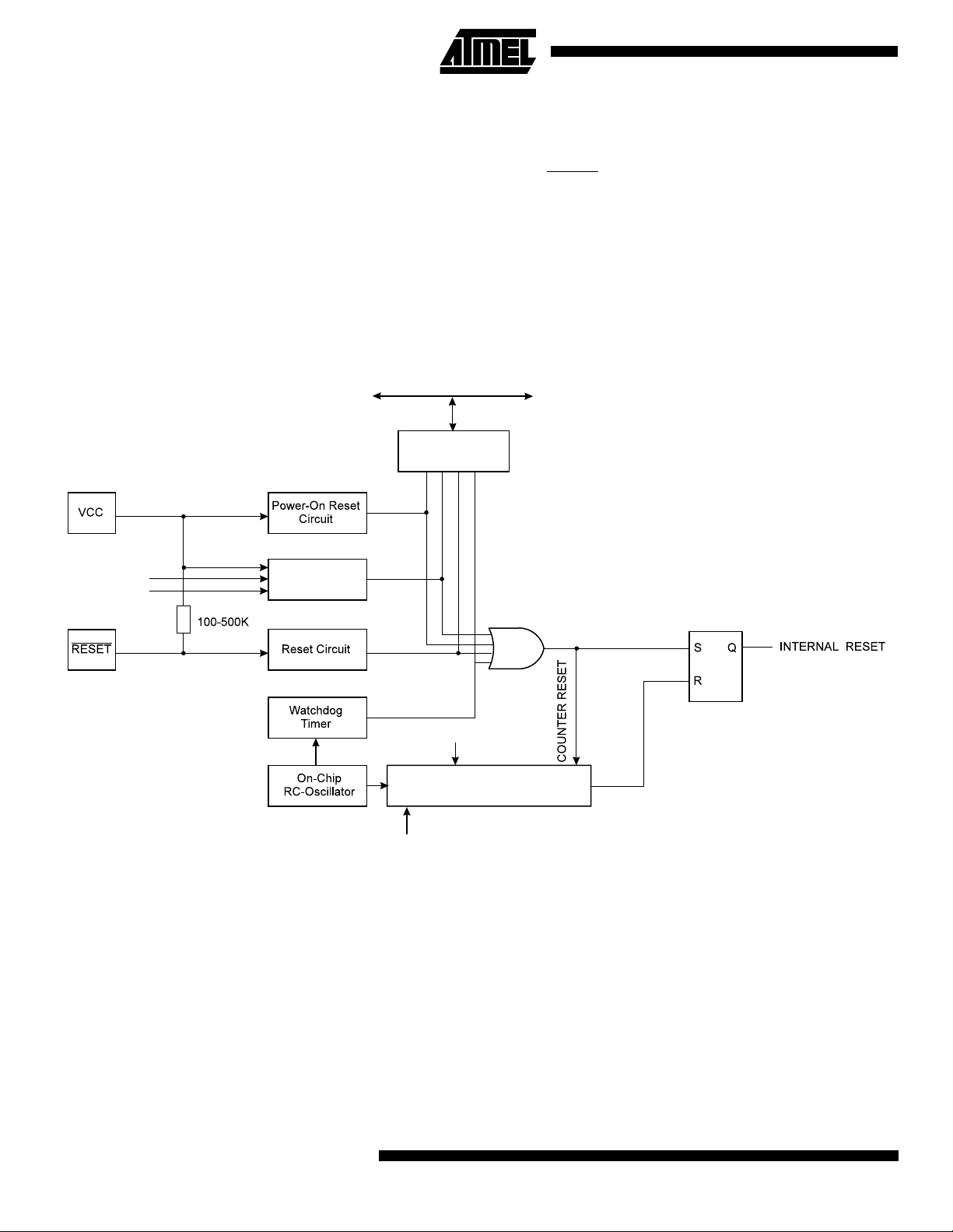
Reset Sources
The ATmega161 has four sources of reset:
• Power-on Reset. The MCU is reset when the supply voltage is below the power-on reset threshold (V
POT
).
• External Reset. The MCU is reset when a low level is present on the RESET pin for more than 500 ns.
• Watchdog Reset. The MCU is reset when the Watchdog timer period expires and the Watchdog is enabled.
• Brown-out Reset. The MCU is reset when the supply voltage V
falls below a certain voltage.
CC
During reset, all I/O regist ers are the n set to their ini tial valu es, and the pro gram starts execution from address $000. The
instruction placed in address $000 must be an JMP – relative jump – instruction to the reset handling routine. If the program
never enables an interrupt source, the interrupt vectors are not used, and regular program code can be placed at thes e
locations. The cir cuit diagram in Figure 24 shows the reset logic. Ta ble 3 and Table 4 define s the timing and elec trical
parameters of the reset circuitry
Figure 24. Reset Logic
DATA BUS
MCU Status
Register (MCUSR)
BORF
WDRF
PORF
EXTRF
BODEN
BODLEVEL
Brown-Out
Reset Circuit
CK
CKSEL[2:0]
Delay Counters
Full
24
ATmega161(L)
Page 25
ATmega161(L)
Table 3. Reset Characteristics (V
= 5.0V)
CC
Symbol Parameter Condition Min Typ Max Units
BOD disabled 1.0 1.4 1.8 V
Power-on Reset Threshold Voltage (rising)
BOD enabled 1.7 2.2 2.7 V
V
POT
BOD disabled 0.4 0.6 0.8 V
Power-on Reset Threshold Voltage (falling)
BOD enabled 1.7 2.2 2.7 V
V
RST
RESET Pin Threshold Voltage - - 0.85 V
CC
(BODLEVEL = 1) 2.6 2.7 2.8
V
BOT
Note: The Power-on Reset will not work unless the supply voltage has been below V
‘
Table 4. Reset Delay Selections
CKSEL
[2:0]
Brown-out R eset Threshold Voltage
Start-up Time, VCC = 2.7V,
BODLEVEL Unprogrammed
(BODLEVEL = 0) 3.8 4.0 4.2
(falling).
POT
Start-up Time, VCC = 4.0V,
BODLEVEL Programmed Recommended Usage
(1)
000 4.2 ms + 6 CK 5.8 ms + 6 CK External Clock, fast rising power
001 30 µs + 6 CK 10 µs + 6 CK External Clock, BOD enabled
(2)(3)
010 67 ms + 16K CK 92 ms + 16K CK Crystal Oscillator, slowly rising power
011 4.2 ms + 16K CK 5.8 ms + 16K CK Crystal Oscillator, fast rising power
100 30 µs + 16K CK 10 µs + 16K CK Crystal Oscillator, BOD enabled
(2)(3)
101 67 ms + 1K CK 92 ms + 1K CK Ceramic Resonator/External clock, Slowly rising power
V
V
110 4.2 ms + 1K CK 5.8 ms + 1K CK Ceramic Resonator, fast rising power
111 30 µs + 1K CK 10 µs + 1K CK Ceramic Resonator, BOD enabled
(2)(3)
Notes: 1. Th e CKSEL fuses con trol only the start-up ti me. The os cillator is the same fo r all sele ctions. On powe r-up, the rea l-ti me part
of the start-up time is increased with typ. 0.6ms.
2. Or external power-on reset.
3. When BOD is enabled, there will be a real-time part = 50 µs (typ.)
Table 4 shows th e start-up time s from reset . From slee p, only the clo ck counting part of the sta rt-up time is used. The
watchdog oscillator is used for timing the real-time part of the start-up time. The number WDT oscillator cycles used for
each time-out is shown in Table 5.
Table 5. Number of Watchdog Oscillator Cycles
BODLEVEL Time-out Number of cycles
Unprogrammed 4.2 ms (at Vcc=2.7V) 1K
Unprogrammed 67 ms (at V
Programmed 5.8 ms (at V
=2.7V) 16K
cc
=4.0V) 4K
cc
Programmed 92 ms (at Vcc=4.0V) 64K
Note: The bod-level fus e ca n b e u se d to s elect start-up times even if the Brown-o ut det ection is disabled (by le av ing th e BO DE N fuse
unprogrammed).
The frequency of the watchdog oscillator is voltage dependent as shown in the Electrical Characteristics section. The
device is shipped with CKSEL = 010.
25
Page 26

Power-on Reset
A Power-on Reset (POR) pulse is generated by an on-chip detection circuit. The detection level is nominally 1.4V (rising
VCC). The POR is activated whenever V
is below the detection level. The POR circuit can be used to trigger the start-up
CC
reset, as well as detect a failure in supply voltage.
A Power-on Reset (POR) circuit ensures that the device is reset from power-on. Reaching the power-on reset threshold
voltage invokes a delay cou nter, which determi nes the delay, for which the devi ce is kept in RE SET after V
rise. The
CC
time-out period of the delay counter can be defined by the user through the CKSEL fuses. The eight different selections for
the delay period are presented in Table 4. The RESET signal is activated again, without any delay, when the V
CC
decreases below detection level.
Figure 25. MCU Start-up, RESET
VCC
RESET
TIME-OUT
INTERNAL
RESET
Figure 26. MCU Start-up, RESET
VCC
RESET
TIME-OUT
Tied to VCC.
V
POT
V
RST
t
TOUT
Controlled Externally
V
POT
V
RST
t
TOUT
INTERNAL
RESET
External Reset
An external reset is generated by a l ow level on the RESET
pin. Reset pulses longer than 500 ns will generate a reset,
even if the clock is not running. Shorter pulses are not guaranteed to generate a reset. When the applied signal reaches the
Reset Threshold Voltage – V
on its positive edge, the delay timer starts the MCU after the Time-out period t
RST
TOUT
has
expired.
26
ATmega161(L)
Page 27
ATmega161(L)
Figure 27. External Reset During Operation
Brown-out Detection
ATmega161 has an o n-chip brown -out dete ction (BOD) circuit for m onitori ng the V
circuit can be enabled/disabled by the fuse BODEN. When BODEN is enabled (BODEN programmed), and V
to a value bel ow t he t rigg er le vel , the b row n-ou t re set is i mmedi ate ly ac tiva te d. Wh en V
the brown-out reset is deactivated after a delay. The delay is defined by the user in the same way as the delay of POR signal, in Table 4. The trig ger level for the BOD can be sel ected by the fuse BODLEV EL to be 2.7V (BODLEVEL
unprogrammed), or 4.0V ((BODLEVEL programmed). The trigger level has a hysteresis of 50 mV to ensure spike free
brown-out detection.
The BOD circuit will only detect a drop in V
if the voltage stays below the trigger level for longer than 9 µs for trigger level
CC
4.0V, 21 µs for trig ger level 2.7V (typical values).
level during the operati on. T he BOD
CC
increases above the trigger level,
CC
decreases
CC
Figure 28. Brown-out Reset During Operation
VCC
RESET
TIME-OUT
INTERNAL
RESET
V
BOT-
V
BOT+
t
TOUT
Watchdog Reset
When the Watchdo g tim es out, it will genera te a sh ort rese t pulse o f 1 XT AL cyc le dur ation. On the fal ling edge of th is
pulse, the delay timer starts counting the Time-out period t
. Refer to Page page 52 for details on operation of the
TOUT
Watchdog.
27
Page 28
Figure 29. Watchdog Reset During Operation
MCU Status Register – MCUSR
The MCU Status Register provides information on which reset source caused an MCU reset.
Bit 76543210
$34 ($54) - - - - WDRF BORF EXTRF PORF MCUSR
Read/Write R R R R R/W R/W R/W R/W
Initial value 0 0 0 0 See bit description
Bits 7..4 - Res: Reserved Bits
•
These bits are reserved bits in the ATmega161 and always read as zero.
Bit 3 - WDRF: Watchdog Reset Flag
•
This bit is set if a watchdog reset occurs. The bit is cleared by a power-on reset, or by writing a logic zero to the flag.
•
Bit 2 - BORF: Brown-out Reset Flag
This bit is set if a brown-out reset occurs. The bit is cleared by a power-on reset, or by writing a logic zero to the flag.
Bit 1 - EXTRF: External Reset Flag
•
This bit is set if an external reset occurs. The bit is cleared by a power-on reset, or by writing a logic zero to the flag.
Bit 0 - PORF: Power-on Reset Flag
•
This bit is set if a power-on reset occurs. The bit is cleared only by writing a logic zero to the flag.
To make use of the reset flags to identify a reset condition, the user should read and then clear the MCUSR as early as
possible in the program. If th e regist er is clear ed before ano ther reset occurs, th e source of th e reset can be found by
examining the reset flags.
Interrupt Handling
The ATmega161 has two 8-bit Interrupt Mask control registe rs; GIMSK – Genera l Interrupt Ma sk register and TIM SK –
Timer/Counter Interrupt Mask register.
When an interrupt occurs, the Global Interrupt Enable I-bit is cleared (zero) and all interrupts are disabled. The user software can set (one) the I-bit to enabl e nested interrupts. The I-bit is set (one) when a Return from Interrupt instruction –
RETI – is executed.
When the Program Counter is vectored to the actual interrupt vector in order to execute the interrupt handling routine, hardware clears the corresponding flag that generated the interrupt. Some of the interrupt flags can also be cleared by writing a
logic one to the flag bit position(s) to be cleared.
If an interrupt condition occurs when the corresponding interrupt enable bit is cleared (zero), the interrupt flag will be set
and remembered until the interrupt is enabled, or the flag is cleared by software.
28
ATmega161(L)
Page 29

ATmega161(L)
If one or more interrupt condi tions occu r when the global interrupt ena ble bit is clea red (zero), th e correspondi ng interrup t
flag(s) will be set and remembered until the global interrupt enable bit is set (one), and will be executed by order of priority.
Note that external level interrupt does not have a flag, and will only be remembered for as long as the interrupt condition is
present.
Note that the status register is not automatically stored when entering an interrupt routine and restored when returning from
an interrupt routine. This must be handled by software.
Interrupt Response Time
The interrupt execut ion respons e for all th e enabled A VR in terrupts is 4 clock cycles mi nimum. Afte r 4 clock cycles th e
program vec tor addre ss for the actual interru pt handl ing ro utine is execute d. Duri ng this 4 cl ock cyc le perio d, the Pr ogra m
Counter (13 bits) is pushed onto the Stack. The vector is normally a jump to the interrupt routine, and this jump takes
3 clock cycles. If an interrupt occurs during execution of a multi-cycle instruction, this instruction is completed before the
interrupt is served. If an interrupt occurs when the MCU is in sleep mode, the interrupt execution response time is
increased by 4 clock cycles.
A return from an interrupt handling routine takes 4 clock cycles. During these 4 clock cycles, the Program Counter (2 bytes)
is popped back from th e St ack , th e St ac k P oi nter is i nc remented by 2, and the I flag in S R E G is set. When AVR exits from
an interrupt, it wi ll always return to the main progr am and ex ecute one more in struction before a ny pendi ng interr upt is
served.
General Interrupt Mask Register – GIMSK
Bit 7 6 5 4 3 2 1 0
$3B ($5B) INT1 INT0 INT2 - - - - - GIMSK
Read/Write R/W R/W R R R R R R
Initial value 0 0 0 0 0 0 0 0
Bit 7 - INT1: External Interrupt Request 1 Enable
•
When the INT1 bit is set (one) and the I-bit in the Status Register (SREG) is set (one), the external pin interrupt is enabled.
The Interrupt Sense Control1 bits 1/0 (ISC11 and ISC10) in the MCU general Control Register (MCUCR) define whether
the external interrupt is ac tivated on rising and/or falli ng edge of the INT1 pin or level sense d. Acti vi ty on the pin will ca use
an interrupt request ev en if INT 1 i s co nfi gur ed as an output. The corresponding interrupt of Exte r nal Inte rrup t Re ques t 1 is
executed from program memory address $004. See also “External Interrupts”.
Bit 6 - INT0: External Interrupt Request 0 Enable
•
When the INT0 bit is set (one) and the I-bit in the Status Register (SREG) is set (one), the external pin interrupt is enabled.
The Interrupt Sense Control0 bits 1/0 (ISC01 and ISC00) in the MCU general Control Register (MCUCR) defines whet her
the external interrupt is ac tivated on rising and/or falli ng edge of the INT0 pin or level sense d. Acti vi ty on the pin will ca use
an interrupt request ev en if INT 0 i s co nfi gur ed as an output. The corresponding interrupt of Exte r nal Inte rrup t Re ques t 0 is
executed from program memory address $002. See also “External Interrupts.”
Bit 5- INT2: External Interrupt Request 2 Enable
•
When the INT2 bit is set (one) and the I-bit in the Status Register (SREG) is set (one), the external pin interrupt is activated.
The Interrupt Sense Control2 bit (ISC02 in the Extended MCU Control Register (EMCUCR) defines whether the external
interrupt is activated on rising or falling edge of the INT2 pin. Activity on the pin will cause an interrupt request even if INT2
is configured as an outp ut. The co rrespo nding inter rupt of Externa l Interru pt Reques t 2 is execute d from program m emory
address $006. See also “External Interrupts.”
Bits 4..0 - Res: Reserved bits
•
These bits are reserved bits in the ATmega161 and always read as zero.
29
Page 30

General Interrupt Flag Register – GIFR
Bit 7 6 5 4 3 2 1 0
$3A ($5A) INTF1 INTF0 INTF2 - - - - - GIFR
Read/Write R/W R/W R/W R R R R R
Initial value 0 0 0 0 0 0 0 0
Bit 7 - INTF1: External Interrupt Flag1
•
When an event on the INT1 pin triggers an interrupt request, INTF1 becomes set (one). If the I-bit in SREG and the INT1 bit
in GIMSK are set (one), the MCU will jump to the interrupt vector at address $004. The flag is cleared when the interrupt
routine is executed. Alternatively, the flag can be cleared by writing a logical one to it.
Bit 6 - INTF0: External Interrupt Flag0
•
When an event on the INT0 pin triggers an interrupt request, INTF0 becomes set (one). If the I-bit in SREG and the INT0 bit
in GIMSK are set (one), the MCU will jump to the interrupt vector at address $002. The flag is cleared when the interrupt
routine is executed. Alternatively, the flag can be cleared by writing a logical one to it.
Bit 5 - INTF2: External Interrupt Flag2
•
When an event on the INT2 pin triggers an interrupt request, INTF2 becomes set (one). If the I-bit in SREG and the INT2 bit
in GIMSK are set (one), the MCU will jump to the interrupt vector at address $006. The flag is cleared when the interrupt
routine is executed. Alternatively, the flag can be cleared by writing a logical one to it.
Bits 4..0 - Res: Reserved bits
•
These bits are reserved bits in the ATmega161 and always read as zero.
Timer/counter Interrupt Mask Register – TIMSK
Bit 7 6 5 4 3 2 1 0
$39 ($59) TOIE1 OCIE1A OCIE1B TOIE2 TICIE1 OCIE2 TOIE0 OCIE0 TIMSK
Read/Write R/W R/W R/W R/W R/W R/W R/W R/W
Initial value 0 0 0 0 0 0 0 0
Bit 7 - TOIE1: Timer/Counter1 Overflow Interrupt Enable
•
When the TOIE1 bit is set (one) and the I-bit in the Status Register is set (one), the Timer/Counter1 Overflow interrupt is
enabled. The corresponding interrupt (at vector $012) is executed if an overflow in Timer/Counter1 occurs, i.e., when the
TOV1 bit is set in the Timer/Counter Interrupt Flag Register – TIFR.
Bit 6 - OCE1A:Timer/Counter1 Output CompareA Match Interrupt Enable
•
When the OCIE1A bit is set (one) and the I-bit in the Status Register is set (one), the Timer/Counter1 CompareA Match
interrupt is enabled. The corresponding interrupt (at vector $00e) is executed if a CompareA match in Timer/Counter1
occurs, i.e., when the OCF1A bit is set in the Timer/Counter Interrupt Flag Register – TIFR.
Bit 5 - OCIE1B:Timer/Counter1 Output CompareB Match Interrupt Enable
•
When the OCIE1B bit is set (one) and the I-bit in the Status Register is set (one), the Timer/Counter1 CompareB Match
interrupt is enabled. The corresponding interrupt (at vector $010) is executed if a CompareB match in Timer/Counter1
occurs, i.e., when the OCF1B bit is set in the Timer/Counter Interrupt Flag Register – TIFR.
Bit 4 - TOIE2: Timer/Counter2 Overflow Interrupt Enable
•
When the TOIE2 bit is set (one) and the I-bit in the Status Register is set (one), the Timer/Counter2 Overflow interrupt is
enabled. The corresponding interrupt (at vector $00a) is executed if an overflow in Timer/Counter2 occurs, i.e., when the
TOV2 bit is set in the Timer/Counter Interrupt Flag Register – TIFR.
Bit 3 - TICIE1: Timer/Counter1 Input Capture Interrupt Enable
•
When the TICIE1 bi t is set (o ne) and the I- bit in the Status Re gister is set (one), th e Time r/Counter 1 Input Capture Ev ent
Interrupt is enabled. The corresponding interrupt (at vector $00C) is executed if a capture-triggering event occurs on pin 31,
ICP, i.e., when the ICF1 bit is set in the Timer/Counter Interrupt Flag Register – TIFR.
Bit 2 - OCIE2:Timer/Counter2 Output Compare Match Interrupt Enable
•
When the OCIE2 bit is set (one) and the I- bit in t he Status Reg is ter is s et (one ), th e Tim er /Cou nter2 Co mpa re Matc h inte rrupt is enabled. T he corre sponding interru pt (at vect or $008) is execu ted if a Comp are2 ma tch in Tim er/Cou nter2 occ urs,
i.e., when the OCF2 bit is set in the Timer/Counter Interrupt Flag Register – TIFR.
30
ATmega161(L)
Page 31

ATmega161(L)
Bit 1 - TOIE0: Timer/Counter0 Overflow Interrupt Enable
•
When the TOIE0 bit is set (one) and the I-bit in the Status Register is set (one), the Timer/Counter0 Overflow interrupt is
enabled. The corresponding interrupt (at vector $016) is executed if an overflow in Timer/Counter0 occurs, i.e., when the
TOV0 bit is set in the Timer/Counter Interrupt Flag Register – TIFR.
Bit 0 - OCIE0: Timer/Counter0 Output Compare Match Interrupt Enable
•
When the OCIE0 bit is set (one) and the I- bit in t he Status Reg is ter is s et (one ), th e Tim er /Cou nter0 Co mpa re Matc h inte rrupt is enabled. T he corre sponding interru pt (at vect or $014) is execu ted if a Comp are0 ma tch in Tim er/Cou nter0 occ urs,
i.e., when the OCF0 bit is set in the Timer/Counter Interrupt Flag Register – TIFR.
Timer/Counter Interrupt Flag Register – TIFR
Bit 7 6 5 4 3 2 1 0
$38 ($58) TOV1 OCF1A OCIFB TOV2 ICF1 OCF2 TOV0 OCF0 TIFR
Read/Write R/W R/W R/W R/W R/W R/W R/W R/W
Initial value 0 0 0 0 0 0 0 0
Bit 7 - TOV1: Timer/Counter1 Overflow Flag
•
The TOV1 is se t (one) wh en an ove rflow oc curs in T imer/Cou nter1. TOV1 is cle ared by h ardware when exe cuting th e
corresponding interrupt handling vector. Alternatively, TOV1 is cleared by writing a logic one to the flag. When the I-bit in
SREG, and TOIE1 (T imer/Counter 1 Overflow In terrupt Enab le), and TOV1 ar e set (one), the Timer/Counte r1 Overflow
Interrupt is executed. In PWM mode, this bit is set when Timer/Counter1 changes counting direction at $0000.
Bit 6 - OCF1A: Output Compare Flag 1A
•
The OCF1A bit is set (one) when compare match occurs between the Timer/Counter1 and the data in OCR1A – Output
Compare Register 1A. OCF1A is cleared by hardware when executing the corresponding interrupt handling vector. Alternatively, OCF1A is cleared by writing a logic one to the flag. When the I-bit in SREG, and OCIE1A (Timer/Counter1 Compare
match InterruptA Enable), and the OCF1A are set (one), the Timer/Counter1 Compare A match Interrupt is executed.
Bit 5 - OCF1B: Output Compare Flag 1B
•
The OCF1B bit is set (one) when compare match occurs between the Timer/Counter1 and the data in OCR1B – Output
Compare Register 1B. OCF1B is cleared by hardware when executing the corresponding interrupt handling vector. Alternatively, OCF1B is cleared by writing a logic one to the flag. When the I-bit in SREG, and OCIE1B (Timer/Counter1 Compare
match InterruptB Enable), and the OCF1B are set (one), the Timer/Counter1 Compare B match Interrupt is executed.
Bit 4 - TOV2: Timer/Counter2 Overflow Flag
•
The bit TOV2 is set (one) when an overflow occurs in Timer/Counter2. TOV2 is cleared by hardware when executing the
corresponding interr upt hand ling ve ctor. Alternat ively, T OV2 is c leared by writin g a logic one to the fl ag. Whe n the SREG
I-bit, and TOIE2 ( Timer/Co unter 2 Over flow Inte rru pt En able), and TO V2 a re set (one ), the T ime r/Counter 2 Ove rflow i nterrupt is executed.
Bit 3 - ICF1: - Input Capture Flag 1
•
The ICF1 bit is set (one) to flag an input capture event, indicating that the Timer/Counter1 value has been transferred to the
input capture register – ICR1. ICF1 is cleared by hardware when executing the corresponding interrupt handling vector.
Alternatively, ICF1 is cleared by writing a logic one to the flag. When the SREG I-bit, and TICIE1 (Timer/Counter1 Input
Capture Interrupt Enable), and ICF1 are set (one), the Timer/Counter1 Capture Interrupt is executed.
Bit 2 - OCF2: Output Compare Flag 2
•
The OCF2 bit is set (one) when compare match occurs between the Timer/Counter2 and the data in OCR2 – Output Compare Registe r 2. O CF2 is c leare d by ha rdware when ex ecu ting th e corr espond ing in terru pt ha ndling vecto r. Alte rnat ively ,
OCF2 is cleared by writing a logic one to the flag. When the I-bit in SREG, and OCIE2 (Timer/Counter2 Compare match
InterruptA Enable), and the OCF2 are set (one), the Timer/Counter2 Compare match Interrupt is executed.
Bit 1 - TOV0: Timer/Counter0 Overflow Flag
•
The bit TOV0 is set (one) when an overflow occurs in Timer/Counter0. TOV0 is cleared by hardware when executing the
corresponding interr upt hand ling ve ctor. Alternat ively, T OV0 is c leared by writin g a logic one to the fl ag. Whe n the SREG
I-bit, and TOIE0 (Timer/Co unter0 Overflow Interrupt Ena ble), and TO V0 are set (one), the Time r/Counter0 Over flow
interrupt is executed.
31
Page 32

Bit 2 - OCF0: Output Compare Flag 0
•
The OCF0 bit is set (one) when compare match occurs between the Timer/Counter0 and the data in OCR0 – Output Compare Registe r 0. O CF0 is c leare d by ha rdware when ex ecu ting th e corr espond ing in terru pt ha ndling vecto r. Alte rnat ively ,
OCF0 is cleared by writing a logic one to the flag. When the I-bit in SREG, and OCIE0 (Timer/Counter0 Compare match
InterruptA Enable), and the OCF0 are set (one), the Timer/Counter0 Compare match Interrupt is executed.
External Interrupts
The external interrupts are triggered by the INT0, INT1 and INT2 pins. Observe that, if enabled, the interrupts will trigger
even if the INT0/INT1/INT2 pins a re config ured a s outpu ts. This feature p rovides a way o f gener ating a software i nterrup t.
The external interrup ts can be trigger ed by a fallin g or rising edge or a low lev el (INT 2 is only an edge tr iggered inter rupt).
This is set up as in dicat ed in th e spe cificati on for the MC U Con trol R egist er – MCUCR (INT0 /INT1) and EMCUC R (INT2).
When the external interrupt is enabled and is configured as level triggered (only INT0/INT1), the interrupt will trigger as long
as the pin is held low.
MCU Control Register – MCUCR
The MCU Control Register contains control bits for general MCU functions.
Bit 76543210
$35 ($55) SRE SRW10 SE SM1 ISC11 ISC10 ISC01 ISC00 MCUCR
Read/Write R/W R/W R/W R/W R/W R/W R/W R/W
Initial value 0 0 0 0 0 0 0 0
Bit 7 - SRE: External SRAM Enable
•
When the SRE bit is se t (one) , the ex ternal data mem o ry i nte rface is enab le d, and the pi n fu nc tio ns A D0- 7 (Po r t A), A8 -1 5
(Port C), ALE (Port E), WR
and RD (Port D) are activated as the alternate pin fu nctions. The SRE bit overrides any pin
direction settings in the respective data direction registers. See Figure 51 – Figure 54 for a description of the external memory pin functions. When the SRE bit is cleared (zero), the external data memory interface is disabled, and the normal pin
and data direction settings are used.
Bit 6 - SRW10: External SRAM Wait State
•
The SRW10 bit is used to se t up ex tra wai t s tate s i n th e exter na l m emo ry i nterfa ce . Se e “Inte rf ace to external memory” on
page 72 for a detailed description.
Bit 5 - SE: Sleep Enable
•
The SE bit must be set (one) to make the MCU enter the sleep mode when the SLEEP instruction is executed. To avoid the
MCU entering the sleep mode unless it is the programmers purpose, it is recommended to set the Sleep Enable SE bit just
before the execution of the SLEEP instruction.
Bit 4 - SM1: Sleep Mode Select bit 1
•
The SM1 bit together with the SM0 control bit in EMCUCR selects between the three available sleep modes as shown in
the follow ing table.
Table 6. Sleep Mode Select
SM1 SM0 Sleep Mode
0 0 Idle Mode
01Reserved
1 0 Power-down
1 1 Power Save
•
Bits 3, 2 - ISC11, ISC10: Interrupt Sense Control 1 bit 1 and bit 0
The External Interrupt 1 is activated by the external pin INT1 if the SREG I-flag and the corresponding interrupt mask in the
GIMSK are set. The level and edges on the external INT1 pin that activate the interrupt are defined in Table 7. The value on
the INT1 pin is sampled before dete cting edges. I f edge o r toggle interr upt is sele cted, pu lses that la st lon ger than one
clock period will generate an interrupt. Shorter pulses are not guaranteed to generate an interrupt. If low level interrupt is
selected, the low level must be held until the completion of the currently executing instruction to generate an interrupt.
32
ATmega161(L)
Page 33

ATmega161(L)
Table 7. Interrupt 1 Sense Control
ISC11 ISC10 Description
0 0 The low level of INT1 generates an interrupt request.
0 1 Any logical change on INT1 generates an interrupt request
1 0 The falling edge of INT1 generates an interrupt request.
1 1 Th e risin g edge of INT1 generates an interrupt request.
Note: When changing the ISC11/ISC10 bits, INT1 must be disabled by clearing its Interrupt Enable bit in the GIMSK Register. Other-
wise an interrupt can occur when the bits are changed.
• Bit 1, 0 - ISC01, ISC00: Interrupt Sense Control 0 bit 1 and bit 0
The External Interrupt 0 is activated by the external pin INT0 if the SREG I-flag and the corresponding interrupt mask is set.
The level and edges on the external INT0 pin that activate the interrupt are defined in Table 8. The value on the INT0 pin is
sampled before detecting edges. If edge or toggle interrupt is selected, pulses that last longer than one clock period will
generate an interrupt. S horte r pulses a re not guarantee d to gen erate an inte rrupt. If low level interr upt is se lecte d, the l ow
level must be held until the completion of the currently executing instruction to generate an interrupt.
Table 8. Interrupt 0 Sense Control
ISC01 ISC00 Description
0 0 The low level of INT0 generates an interrupt request.
0 1 Any logical change on INT0 generates an interrupt request
1 0 The falling edge of INT0 generates an interrupt request.
1 1 Th e risin g edge of INT0 generates an interrupt request.
Note: When changing the ISC01/ISC00 bits, INT0 must be disabled by clearing its Interrupt Enable bit in the GIMSK Register. Other-
wise an interrupt can occur when the bits are changed.
Extended MCU Control Register – EMCUCR
The Extended MCU Control Register contains control bits for external interrupt 2, sleep mode bit and control bits for the
external memory interface.
Bit 76543210
$36 ($56) SM0 SRL2 SRL1 SRL0 SRW01 SRW00 SRW11 ISC2 EMCUCR
Read/Write R/W R/W R/W R/W R/W R/W R/W R/W
Initial value 0 0 0 0 0 0 0 0
Bit 7 - SM0: Sleep mode bit 0
•
When this bit is set (one) and sleep mode bit 1 (SM1) in MCUCR is set, Po wer Save Mode is selec ted as sleep mod e.
Refer to page 34 for a detailed description of the sleep modes.
•
Bit 6..4 - SRL2, SRL1, SRL0: External SRAM limit
It is possible to configure different wait-states for different external memory addresses in ATmega161. The SRL2 – SRL0
bits are used to define at which a ddress the differe nt wait- states wil l be co nfigured . See “Interfa ce to externa l memor y” on
page 72 for a detailed description.
Bit 3..1 - SRW01, SRW00, SRW11: External SRAM wait-state select bits.
•
The SRW01, SRW00 and SRW11 bits are used to set up extra wait states in the external memory interface. See “Interface
to external memory” on page 72 for a detailed description.
Bit 0 - ISC2: Interrupt Sense Control 2
•
The external interrupt 2 is activated by the external pin INT2 if the SREG I-flag and the corresponding interrupt mask in the
GIMSK are set. If ISC 2 i s cle ared (zero) a falling edge on I N T2 ac tivates the interrupt. If IS C2 i s se t (one ) a r isin g ed ge o n
INT2 activates the i nte rrup t. E dge s on I N T2 ar e regi ste re d a sync hr ono us ly. P ul se s on IN T2 wi der th an 5 0 n s w il l gener a te
an interrupt. Shorter pulses are not guaranteed to generate an interrupt.
33
Page 34

Sleep Modes
To enter any of the three sleep modes, the SE bit in MCUCR must be set (one) and a SLEEP instruction must be executed.
The SM1 bit in the MCUCR regist er and SM0 bit in the EMCUCR registe r select whi ch sleep mode (Idle, Power-d own, or
Power Save) will be act ivated by the SL EEP in struct ion, see Tabl e 6. If an enabled in terrup t occurs whil e the MCU is in a
sleep mode, the MCU awa kes. T he CPU is the n halt ed for 4 c ycles, i t exe cutes th e inte rrupt ro utine, and r esumes execution from the instruction following SLEEP. The contents of the register file, SRAM, and I/O memory are unaltered. If a reset
occurs during sleep mode, the MCU wakes up and executes from the Reset vector
Idle Mode
When the SM1/SM0 bits are set to 00, the SLEEP ins truction mak es the MCU en ter the Idle Mo de, stopp ing the CPU but
allowing SPI, UARTs, Analog Comparator, Timer/Counters, Watchdog and the interrupt system to continue operating. This
enables the MCU to wake -u p from ex ter na l tri gge red i nter rupt s a s wel l as i nte rnal ones like the Time r Ov erfl ow an d UA RT
Receive Complete interrupts. If wake-up from the Analog Comparator interrupt is not required, the Analog Comparator can
be powered down by setting the ACD-bit in the Analog Comparator Control and Status register – ACSR. This will reduce
power consumption in Idle Mode.
Power-down Mode
When the SM1/SM0 bits are set to 10, the SLEEP instruction makes the MCU enter the Power-down Mode. In this mode,
the external oscillator is stopped, while the external interrupts and the Watchdog (if enabled) continue operating. Only an
external reset, a watchdog reset (if enabled), an external level interrupt on INT0 or INT1, or an external edge interrupt on
INT2 can wake-up the MCU.
If INT2 is used for wake-up from power-down mode, the edge is remembered until the MCU wakes up.
If a level trigger ed in terrupt is u sed fo r wake- up from po wer-down mode, the c hanged leve l mus t be h eld fo r so me tim e to
wake-up the MCU. This makes the MCU less sensitive to noise. The changed level is sampled twice by the watchdog oscillator clock, and if the input has the required level during this time, the MCU will wake-up. The period of the watchdog
oscillator is 1 µs (nominal) at 5.0V and 25C. The frequency of the watchdog oscillator is voltage dependent as shown in the
Electrical Characteristics section.
When waking up from Power-down Mode, there is a delay from the wake-up condition occurs until the wake-up becomes
effective. This a llows the clo ck to r estart a nd bec ome s table after havi ng bee n stop ped. The wake- up pe riod is defi ned by
the same CKSEL fus es t hat def ine the reset time-out period. The wak e-up per i od is equal to the cl ock c oun ting p ar t o f th e
reset period, as shown in Table 4. If the wake-up condition disappears before the MCU wakes up and starts to execute,
e.g. a low level on INT0 is not held long enough, the interrupt causing the wake-up will not be executed.
Power Save Mode
When the SM1/SM0 bits are 11, the SLEEP instruction makes the MCU enter the Power Save Mode. This mode is identical
to Power-down, with one exception:
If Timer/Counter2 is clock ed asy nch r onou sl y, i.e. th e AS2 bi t in AS S R is set, T imer /Co unte r2 will run dur in g sl ee p. In add ition to the Power-down wake-up sources, the device can also wake-up from either Timer Overflow or Output Compare
event from Timer/Counter2 if the corresponding Timer/Counter2 interrupt enable bits are set in TIMSK and the global interrupt enable bit in SREG is set.
Timer/Counters
The ATmega161 provides thre e gene ral pur po se Timer /Co unte rs – tw o 8-bit T /Cs and one 16-b it T/C. T ime r/Coun ter 2 ca n
optionally be asynch ronously clocked from an external osci llator. This oscillator is optimized for us e with a 32.768 kHz
watch crystal, enablin g use o f Tim er/Counter 2 as a Real Tim e Clock ( RTC). Timer/ Counte rs 0 and 1 have indi vidua l pre scaling sele cti on f ro m the s am e 10- b i t prescaling ti me r . T i me r/ Co un t er 2 ha s it s own p re sca le r. B o th th es e pr es ca le rs ca n be
reset by setting the corresponding control bits in the Special Functions IO Register (SFIOR). Refer to page 36 for a detailed
description. These Timer/Counters can either be used as a timer with an internal clock time-base or as a counter with an
external pin connection which triggers the counting.
34
ATmega161(L)
Page 35

Timer/Counter Prescalers
Figure 30. Prescaler for Timer/Counter0 and 1
PSR10
ATmega161(L)
Clear
TCK1 TCK0
For Timer/Counters 0 and 1, the four prescaled selections are: CK/8, CK/64, CK/256 and CK/1024, where CK is the oscillator clock. For the two Timer/Counters 0 and 1, CK, external source, and stop, can also be selected as clock sources.
Setting the PSR10 bit in SFIOR resets the prescaler. This allows the user to operate with a predictable prescaler. Note that
Timer/Counter1 and Timer/Counter 0 share the same prescaler and a prescaler reset will affect both Timer/Counters.
35
Page 36

Figure 31. Timer/Counter2 Prescaler
CK
TOSC1
AS2
PSR2
CS20
CS21
CS22
PCK2
Clear
10-BIT T/C PRESCALER
PCK2/8
PCK2/64
PCK2/32
PCK2/128
0
TIMER/COUNTER2 CLOCK SOURCE
TCK2
PCK2/256
PCK2/1024
The clock source for Timer/Counter2 prescaler is named PCK2. PCK2 is by default connected to the main system clock
CK. By setting the AS2 bit in ASSR, Timer/Counter2 is asynchronously clocked from the PD4(TOSC1) pin. This enables
use of Timer/Counter2 as a Real Time Clock (RTC). When AS2 is set, pins PD4(TOSC1) and PD5(TOSC2) are disconnected from Por t D. A crystal c an then be co nnected between the P D4(TOSC 1) and PD5(T OSC2) pi ns to serve as an
independent clock source for Timer/Counter2. The oscillator is optimized for use with a 32.768 kHz crystal. Alternatively, an
external clock signal can be applied to PD4(TOSC1). The frequency of this clock must be lower than one fourth of the CPU
clock and not higher than 256 kHz. Setting the PSR2 bit in SFIOR resets the prescaler. This allows the user to operate with
a predictable prescaler.
Special Function IO Register – SFIOR
Bit 7 6 5 4 3 2 1 0
$30 ($50) - - - - - - PSR2 PSR10 SFIOR
Read/Write R R R R R R R/W R/W
Initial value 0 0 0 0 0 0 0 0
Bit 7..2 - Res: Reserved Bits
•
These bits are reserved bits in the ATmega161 and always read as zero.
Bit 1 - PSR2: Prescaler Reset Timer/Counter2
•
When this bit is set (one) the Timer/Counter2 prescaler will be reset. The bit will be cleared by hardware after the operation
is performed. Writi ng a z ero to thi s bit will have no e ffect. T his bi t will always be rea d as zer o if Timer/ Counter2 i s cl ocked
by the internal CPU clock. If this bit is written when Timer/Counter2 is operating in asynchronous mode however, the bit will
remain as one until the prescaler has been reset. See “Asynchronous Operation of Timer/Counter2” on page 43 for a
detailed description of asynchronous operation.
Bit 0 - PSR10: Prescaler Reset Timer/Counter1 and Timer/Counter0
•
When this bit is set (one) the Timer/Counter1 and Timer/Counter0 prescaler will be reset. The bit will be cleared by hardware after the operation is performed . Writing a zero to this bit will have no effect. Note tha t Timer/Counter1 and
Timer/Counter0 share the same prescaler and a reset of this prescaler will affect both timers. This bit will always be read as
zero.
36
ATmega161(L)
Page 37

ATmega161(L)
8-bit Timers/Counters T/C0 and T/C2
Figure 32 shows the block diagram for Timer/Counter0. Figure 33 shows the block diagram for Timer/Counter2.
Figure 32. Timer/Counter0 Block Diagram
OCIE1B
OCIE1A
TICIE1
TOIE2
TOIE1
TIMER INT. MASK
REGISTER (TIMSK)
OCIE2
TOIE0
OCIE0
T/C0 OVER-
FLOW IRQ
T/C0 COMPARE
MATCH IRQ
TIMER INT. FLAG
REGISTER (TIFR)
TOV2
TOV1
OCF1B
OCF1A
ICF1
OCF2
TOV0
TOV0
OCF0
REGISTER (TCCR0)
FOC0
OCF0
T/C0 CONTROL
CTC0
PWM0
COM00
COM01
CS02
CS01
SPECIAL FUNCTIONS
IO REGISTER (SFIOR)
CS00
PSR2
PSR10
8-BIT DATA BUS
7
TIMER/COUNTER0
(TCNT0)
7
8-BIT COMPARATOR
7
OUTPUT COMPARE
REGISTER0 (OCR0)
Figure 33. Timer/Counter2 Block Diagram
OCIE1B
TOIE2
(TCNT2)
TICIE1
OCIE2
OCIE1A
TOIE1
TIMER INT. MASK
REGISTER (TIMSK)
7
TIMER/COUNTER2
7
8-BIT COMPARATOR
TOIE0
0
0
0
OCIE0
0
0
T/C CLEAR
T/C CLK SOURCE
UP/DOWN
T/C2 OVER-
FLOW IRQ
OCF2
TIMER INT. FLAG
REGISTER (TIFR)
TOV1
T/C CLEAR
T/C CLK SOURCE
UP/DOWN
T/C2 COMPARE
MATCH IRQ
TOV2
TOV2
OCF1A
OCF1B
8-BIT DATA BUS
8-BIT ASYNCH T/C2 DATA BUS
REGISTER (TCCR2)
TOV0
OCF0
FOC2
ICF1
OCF2
CONTROL
LOGIC
T/C2 CONTROL
CTC2
PWM2
COM21
COM20
CONTROL
LOGIC
CS22
CS21
CS20
CK
T0
SPECIAL FUNCTIONS
IO REGISTER (SFIOR)
PSR2
CK
TOSC1
PSR10
7
OUTPUT COMPARE
REGISTER2 (OCR2)
0
TCK2
ASYNCH. STATUS
REGISTER (ASSR)
AS2
TC2UB
ICR2UB
CK
SYNCH UNIT
OCR2UB
37
Page 38

The 8-bit Timer/Counter0 can select clock source from CK, prescaled CK, or an external pin.
The 8-bit Timer/Count er2 can select clock source from CK, prescaled CK or external TO SC1.
Both Timers/Counters can be stopped as described in section “Timer/Counter0 Control Register – TCCR0” on page 38 and
“Timer/Counter2 Control Register – TCCR2” on page 38
The various status flags (overflow and compare match) are found in the Timer/Counter Interrupt Flag Register – TIFR. Con-
trol signals are found in the Timer/Counter Control Register – TCCR0 and TCCR2. The interrupt enable/disable settings
are found in the Timer/Counter Interrupt Mask Register – TIMSK.
When Timer/Counter0 is externally clocked, the external signal is synchronized with the oscillator frequency of the CPU. To
assure proper sampling of the external clock, the minimum time between two external clock transitions must be at least one
internal CPU clock period. The external clock signal is sampled on the rising edge of the internal CPU clock.
The 8-bit Timer/Counters feature both a high resolution and a high accuracy usage with the lower prescaling opportunities.
Similarly, the high prescaling opportunities make the Timer/Counter0 useful for lower speed functions or exact timing functions with infrequent actions.
Timer/Counter0 and 2 can al so be used as 8-bit Pulse Width Modulato rs. In this mode , the Timer/Co unter and the output
compare register serve as a glitch-free, stand-alone PWM with centered pulses. Refer to page 41 for a detailed description
on this function.
Timer/Counter0 Control Register – TCCR0
Bit 7 6 5 4 3 2 1 0
$33 ($53) FOC0 PWM0 COM01 COM00 CTC0 CS02 CS01 CS00 TCCR0
Read/Write R/W R/W R/W R/W R/W R/W R/W R/W
Initial value 0 0 0 0 0 0 0 0
Timer/Counter2 Control Register – TCCR2
Bit 7 6 5 4 3 2 1 0
$27 ($47) FOC2 PWM2 COM21 COM20 CTC2 CS22 CS21 CS20 TCCR2
Read/Write R/W R/W R/W R/W R/W R/W R/W R/W
Initial value 0 0 0 0 0 0 0 0
Bit 7 - FOC0/FOC2: Force Output Compare
•
Writing a logical one to this bit, forces a change in the compare match output pin PB0 (Timer/Cou nter0) and PB1
(Timer/Counter2) acc ordin g to the va lu es al ready s et in CO M n1 a nd C OM n0. If th e CO Mn 1 a nd CO M n0 b its a re writte n i n
the same cycle as F OC0/F OC2, th e new s ettings wi ll no t take effec t unti l next compa re ma tch or Forc ed Output Compar e
match occurs. The Force Output Compare bit can be used to change the output pin without waiting for a compare match in
the timer. The automatic action programmed in COMn1 and COMn0 happens as if a Compare Match had occurred, but no
interrupt is generated and the Timer/Counters will not be cleared even if CTC0/CTC2 is set. The FOC0/FOC2 bits will
always be read as zero. The setting of the FOC0/FOC2 bits has no effect in PWM mode.
Bit 6 - PWM0/PWM2: Pulse Width Modulator Enable
•
When set (one) this bit enables PWM mode for Timer/Counter0 or Timer/Counter2. This mode is described on page 41.
•
Bits 5,4 - COM01, COM00/COM21, COM20: Compare Output Mode, bits 1 and 0
The COMn1 and COMn0 control bits determine any output pin acti on followin g a compare mat ch in Timer/ Counter0 or
Timer/Counter2. Output pin actions affect pins PB0(OC0) or PB1(OC2). This is an alternative function to an I/O port, and
the corresponding direction control bit must be set (one) to control an output pin. The control configuration is shown in
Table 9.
38
ATmega161(L)
Page 39

ATmega161(L)
Table 9. Compare Mode Select
COMn1 COMn0 Description
0 0 Timer/Counter disconnected from output pin OCn
0 1 Toggle the OCn output line.
1 0 Clear the OCn output line (to zero).
1 1 Set the OCn output line (to one).
Notes: 1. In PWM mode, these bits have a different function. Refer to Table 12 for a detailed description.
2. n = 0 or 2
• Bit 3 - CTC0/CTC2: Clear Timer/Counter on Compare Match
When the CTC0 or CTC2 co ntr ol bit i s se t (one), Timer/Counter0 or Ti mer/ Co unte r2 is res et to $00 in the CP U c lo ck c ycl e
after a compare match. I f the cont rol bit is c leared, Ti mer/Coun ter conti nues coun ting and is unaffec ted by a co mpare
match. When a prescaling of 1 is used, and the compare register is set to C, the timer will count as follows if CTC0/CTC2 is
set:
... | C-1 | C | 0 | 1 | ...
When the prescaler is set to divide by 8, the timer will count like this:
... | C-1, C-1, C-1, C-1, C-1, C-1, C-1, C-1 | C, C, C, C, C, C, C, C | 0, 0, 0, 0, 0, 0, 0, 0 | 1, 1, 1, ...
In PWM mode, this bit has a different function. If the CTC0 or CTC2 bit is cleared in PWM mode, the Timer/Counter acts as
an up/down counter. If the CTC0 or CTC2 bit is set (one), the Timer/Counter wraps when it reaches $FF. Refer to page 41
for a detailed description.
Bits 2,1,0 - CS02, CS01, CS00/ CS22, CS21, CS20: Clock Select bits 2,1 and 0
•
The Clock Select bits 2,1 and 0 define the prescaling source of Timer/Counter0 and Timer/Counter2.
Table 10. Clock 0 Prescale Select
CS02 CS01 CS00 Description
0 0 0 Stop, the Timer/Counter0 is stopped.
001CK
010CK/8
011CK/64
100CK/256
101CK/1024
1 1 0 External Pin PB0(T0), falling edge
1 1 1 External Pin PB0(T0), rising edge
39
Page 40

Table 11. Clock 2 Prescale S elect
CS22 CS21 CS20 Description
0 0 0 Stop, the Timer/Counter2 is stopped.
0 0 1 PCK2
0 1 0 PCK2/8
0 1 1 PCK2/32
1 0 0 PCK2/64
1 0 1 PCK2/128
1 1 0 PCK2/256
1 1 1 PCK2/1024
The Stop condition provides a Timer Enable/Disable function. The prescaled modes are scaled directly from the CK oscillator clock for Timer/Counter0 and PCK2 for Timer/Counter2. If the external pin modes are used for Timer/Counter0,
transitions on PB0/( T0) will c lock the counte r even if the pi n is confi gured as an outp ut. This feature can gi ve the user SW
control of the counting.
Timer Counter0 – TCNT0
Bit 76543210
$32 ($52) MSB LSB TCNT0
Read/Write R/W R/W R/W R/W R/W R/W R/W R/W
Initial value00000000
Timer/Counter2 – TCNT2
Bit 76543210
$23 ($43) MSB LSB TCNT2
Read/Write R/W R/W R/W R/W R/W R/W R/W R/W
Initial value00000000
These 8-bit registers contain the value of the Timer/Counters.
Both Timer/Counters is realized as up or up/down (in PWM mode) counters with read and write access. If the
Timer/Counter is wri tten to an d a cloc k sou rce is s elected , it contin ues coun tin g in the timer clock cycl e foll owing t he write
operation.
Timer/Counter0 Output Compare Register – OCR0
Bit 76543210
$31 ($51) MSB LSB OCR0
Read/Write R/W R/W R/W R/W R/W R/W R/W R/W
Initial value00000000
Timer/Counter2 Output Compare Register – OCR2
Bit 76543210
$22 ($42) MSB LSB OCR2
Read/Write R/W R/W R/W R/W R/W R/W R/W R/W
Initial value00000000
40
ATmega161(L)
Page 41

ATmega161(L)
The output compare registers are 8-bit read/write register s. The Timer/Counter Output Compar e Registers contains the
data to be continuously compared with the Timer/Counter. Actions on compare matches are specified in TCCR0 and
TCCR2. A compare match does only occu r if the Timer/Counter counts to the OCR value. A s oftware write that sets
Timer/Counter and Output Compare Register to the same value does not generate a compare match.
A compare match will set the compare interrupt flag in the CPU clock cycle following the compare event.
Timer/Counter 0 and 2 in PWM Mode
When PWM mode is selected, the Timer/Counter either wraps (overflows) when it reaches $FF or it acts as an up/down
counter.
If the up/down mode is selected, the Timer/Counter and the Output Compare Registers – OCR0 or OCR2 form an 8-bit,
free-running, glitch-free and phase correct PWM with outputs on the PB0(OC0/PWM0) or PB1(OC2/PWM2) pin.
If the overflow mode is selected, the Timer/Counter and the Output Compare Registers – OCR0 or OCR2 form an 8-bit,
free-running and glitch-free PWM, operating with twice the speed of the up/down counting mode.
PWM Modes (Up/Down and Overflow)
The two different PWM modes are sele cted by the CTC0 or CTC2 bi t in the Timer/Counter Cont rol Register s – TCCR0 or
TCCR2 respectively.
If CTC0/CTC2 is cleared and PWM mode is selected, the Timer/Counter acts as an up/down counter, counting up from $00
to $FF, where it turns and counts down again to zero before the cycle is repeated. When the counter value matches the
contents of the Output Compare Register, the PB0(OC0/PWM0) or PB1(OC2/PWM2) pin is set or cleared according to the
settings of the COMn1/COMn0 bits in the Timer/Counter Control Registers TCCR0 or TCCR2.
If CTC0/CTC2 is set and P WM mode i s sel ected, th e T imer/Cou nters w ill wrap and start coun ting f rom $00 af ter rea ching
$FF. The PB0(OC0/P WM0) or PB1 (OC2/PW M2) pin wil l be set o r cl eared ac cor ding to the set tings of COM n1/COMn0 o n
a Timer/Counter overflow or when the counter value matches the contents of the Output Compare Register. Refer to Table
12 for details.
Table 12. Compare Mode Select in PWM Mode
CTCn COMn1 COMn0 Effect on Compare Pin Frequency
0 0 0 Not connected
0 0 1 Not connected
01 0
01 1
1 0 0 Not connected
1 0 1 Not connected
1 1 0 Cleared on compare match, set on overflow. f
1 1 1 Set on compare match, cleared on overflow. f
Note: n = 0 or 2
Cleared on compare match, up-counting. Set on compare match,
down-counting (non-inverted PWM).
Cleared on compare match, down-counting. Set on compare match,
up-counting (inverted PWM).
f
TCK0/2
f
TCK0/2
TCK0/2
TCK0/2
/510
/510
/256
/256
Note that in PWM mode, the value to be written to the Output Compare Register is first transferred to a temporary location,
and then latched into the OCR when the Timer/Counter reaches $FF. This prevents the occurrence of odd-length PWM
pulses (glitches) in the event of an unsynchronized OCR0 or OCR2 write. See Figure 34 and Figure 35 for examples.
41
Page 42

Figure 34. Effects of Unsynchronized OCR Latching in up/down mode
Compare Value changes
Synchronized OCn Latch
Compare Value changes
Counter Value
Compare Value
PWM Output OCn
Counter Value
Compare Value
PWM Output OCn
Unsynchronized OCn Latch
Glitch
Figure 35. Effects of Unsynchronized OCR Latching in overflow mode.
Compare Value changes
Counter Value
Compare Value
PWM Output OCn
Synchronized OCn Latch
Compare Value changes
Counter Value
Compare Value
PWM Output OCn
Unsynchronized OCn Latch
Note: n = 0 or 2 (Figure 34 and Figure 35)
Glitch
During the time between the write and the latch operation, a read from the Output Compare Registers will read the contents
of the temporary location. This means that the most recently written value always will read out of OCR0 and OCR2.
When the Out put Compare Re gister contain s $00 or $FF, and the up/dow n PWM mode is selected, the output
PB0(OC0/PWM0)/PB1(OC2/PWM2) is updated to low or high on the next compare match according to the settings of
COMn1/COMn0. This is shown in Table 13. In overflow PWM mode, the output PB0(OC0/PWM0)/PB1(OC2/PWM2) is held
low or high only when the Output Compare Register contains $FF.
Table 13. PWM Outputs OCRn = $00 or $FF
COMn1 COMn0 OCRn Output PWMn
10$00 L
10$FF H
11$00 H
11$FF L
Note: n = 0 or 2
In overflow PWM mode, the table above is only valid for OCRn = $FF.
42
ATmega161(L)
Page 43

ATmega161(L)
In up/down PWM mode, the T imer O ver flow Flag, TOV0 or TOV2, is set when the c oun ter adv an ce s fr om $00 . In ov erfl ow
PWM mode, the Timer Overflow Flag is set as in normal Timer/Counter mode. Timer Overflow Interrupt0 and 2 operate
exactly as in normal Timer/Counter mode, i.e. they are executed when TOV0 or TOV2 are set provided that Timer Overflow
Interrupt and global interrupts are enabled. This does also apply to the Timer Output Compare flag and interrupt.
Asynchronous Status Register – ASSR
Bit 76543 2 1 0
$26 ($46) - - - - AS2 TCN2UB OCR2UB TCR2UB ASSR
Read/Write R R R R R/W R R R
Initial value 0 0 0 0 0 0 0 0
Bit 7..4 - Res: Reserved Bits
•
These bits are reserved bits in the ATmega161 and always read as zero.
Bit 3 - AS2: Asynchronous Timer/Counter2 mode
•
When this bit is cleared (zero) Timer/Counter2 is clocked from the inter nal system clock, CK. If AS2 is set, the
Timer/Counter2 is clocked from the TOSC1 pin. Pins PD4 and PD5 become connected to a crystal oscillator and cannot be
used as general I/O pins. When the value of this bit is changed the contents of TCNT2, OCR2 and TCCR2 might get
corrupted.
Bit 2 - TCN2UB: Timer/Counter2 Update Busy
•
When Timer/Counter2 operates asynchronously and TCNT2 is written, this bit becomes set (one). When TCNT2 has been
updated from th e tempora ry sto rage reg ister, th is bit is cl eared ( zero) by ha rdwar e. A log ical zero in this bit indic ates tha t
TCNT2 is ready to be updated with a new value.
Bit 1 - OCR2UB: Output Compare Register2 Update Busy
•
When Timer/Counter2 operates asynchronously and OCR2 is written, this bit becomes set (one). When OCR2 has been
updated from th e tempora ry sto rage reg ister, th is bit is cl eared ( zero) by ha rdwar e. A log ical zero in this bit indic ates tha t
OCR2 is ready to be updated with a new value.
Bit 0 - TCR2UB: Timer/Counter Control Register2 Update Busy
•
When Timer/Counter2 operates asynchronously and TCCR2 is written, this bit becomes set (one). When TCCR2 has been
updated from th e tempora ry sto rage reg ister, th is bit is cl eared ( zero) by ha rdwar e. A log ical zero in this bit indic ates tha t
TCCR2 is ready to be updated with a new value.
If a write is performed to any of the three Timer/Counter2 registers while its update busy flag is set (one), the updated value
might get corrupted and cause an unintentional interrupt to occur.
The mechanisms for reading TCNT 2, OCR2, and T CCR2 are different. W hen read ing TCNT2, the actual ti mer value is
read. When reading OCR2 or TCCR2, the value in the temporary storage register is read.
Asynchronous Operation of Timer/Counter2
When Timer/Counter2 operates asynchronously, some considerations must be taken.
• Warning: When switching between asynchronous and synchronous clocking of Timer/Counter2, the timer registers;
TCNT2, OCR2 and TCCR2 might get corrupted. A safe procedure for switching clock source is:
1. Disable the Timer/Counter2 interrupts by clearing OCIE2 and TOIE2.
2. Select clock source by setting AS2 as appropriate.
3. Write new values to TCNT2, OCR2, and TCCR2.
4. To switch to asynchronous operation: Wait for TCN2UB, OCR2UB, and TCR2UB.
5. Enable interrupts, if needed.
• The oscillator is optimized for use with a 32,768 Hz watch crystal. An external clock signal applied to this pin g oes
through the same amplifie r having a bandwidt h of 256 k Hz. The extern al clock sign al should ther efore be in the int erval
0 Hz - 256 kHz. The frequenc y of the clock sig nal applied to the TOSC1 pin must be lowe r than one four th of the CPU
main clock frequency.
43
Page 44

• When writing to one of the registers TCNT2 , OCR2, or TCCR2, the value is transferred to a temporary register, and
latched after two positi ve e dge s on TOSC1 . The us er should not write a new value before the contents of the temporary
register have been tran sferred to its des tination. Each of the three mentioned reg isters have their in dividual tempo rary
register, which means that e.g. writing to TCNT2 does not disturb an OCR2 write in progress. To detect that a transfer to
the destination register has taken place, a Asynchronous Status Register – ASSR has been implem ente d.
• When entering Power Save mode after having written to TCNT2 , OCR2, or TCCR2, the user mus t wait until the written
register has been update d if Timer/Counter 2 is used t o wake-up the d evice. O therwis e, the MCU wi ll go t o sleep bef ore
the changes have ha d any effect. This is e xtremely import ant if the Output Com pare2 interrupt is u sed to wake-up th e
device; Output compare is disabled during write to OCR2 or TCNT2. If the write cycle is not finished (i.e. the MCU enters
sleep mode before the OCR2 UB bit returns to zero), the dev ice will never get a com pare match and the MCU will not
wake-up.
• If Timer/Counter2 is used to wake-up the device from Po wer Sav e mod e, pr eca utions mus t be taken if the user wants to
re-enter Power Save mode : The interrupt logic ne eds one TOSC1 cycle to be rese t. If the time between wake -up and
re-entering Power Save mode is less than one TOSC1 cycle, the interrupt will not occur and the device will fail to
wake-up. If the user is in do ubt wh eth er the ti me b efor e re- en ter in g P ower Sa ve is sufficient, the followi ng a lgo rithm ca n
be used to ensure that one TOSC1 cycle has elapsed:
1. Write a value to TCCR2, TCNT2, or OCR2
2. Wait until the corresponding Update Busy flag in ASSR returns to zero.
3. Enter Power Save mode
• When asynchronous ope rati on is sel ected, the 32 kH z osci llator for Timer/Counter2 is alway s runni ng, excep t in p ower-
down mode. After a power-up reset or wake-up from power-down, the user should be aware of the fact that this oscillator
might take as long as one secon d to stabilize. Therefore, th e contents of all Timer2 registers must be con sidered lost
after a wake-up from pow er-down, due to the u nstable cl ock signal . The user is advised t o wait for at least one s econd
before using Timer/Counter2 after power-up or wake-up from power-down.
• Description of wake-up from power save mode when the timer is clocked asynchronously: When the interrupt condition is
met, the wake-up process is star ted on th e follow ing cyc le of the ti mer cloc k, tha t is, the timer is always a dvanced by at
least one before the process or can read the counter value. The inte rrupt flags are updated 3 pro cessor cyc les after the
processor clock h as started. During these c ycles, the pr ocessor exe cutes instructi ons, but the in terrupt con dition is not
readable, and the interrupt routine has not started yet.
• During asynchronous o peration, the synchroniz ation of the interrupt fla gs for the as ynchrono us timer take s 3 process or
cycles plus one timer cyc le. The timer is therefore advanced by at l east one before the processor can read the timer
value causing the setting of the interrupt flag. The output compare pin is changed on the timer clock and is not
synchronized to the processor clock.
44
ATmega161(L)
Page 45

Timer/Counter1.
Figure 36 shows the block diagram for Timer/Counter1.
Figure 36. Timer/Counter1 Block Diagram
ATmega161(L)
OCIE1B
OCIE1A
TOIE1
TIMER INT. MASK
REGISTER (TIMSK)
8-BIT DATA BUS
T/C1 OVER-
FLOW IRQ
OCIE2
TICIE1
TOIE2
T/C1 COMPARE
MATCHA IRQ
TOIE0
OCIE0
TOV1
OCF1B
OCF1A
T/C1 COMPARE
MATCHB IRQ
OCF2
ICF1
TOV2
TOV0
TIMER INT. FLAG
REGISTER (TIFR)
ICF1
TOV1
OCF1B
OCF1A
TOV2
OCF2
TOV0
T/C1 INPUT CAPTURE REGISTER (ICR1)
CAPTURE
TRIGGER
TIMER/COUNTER1 (TCNT1)
T/C1 INPUT
CAPTURE IRQ
OCF0
T/C1 CONTROL
REGISTER A (TCCR1A)
OCF0
COM1A1
COM1A0
COM1B0
07815
07815
T/C CLEAR
T/C CLOCK SOURCE
UP/DOWN
FOC1A
COM1B1
FOC1B
PWM11
T/C1 CONTROL
REGISTER B (TCCR1B)
ICES1
ICNC1
PWM10
CONTROL
LOGIC
CTC1
CS12
CS11
SPECIAL FUNCTIONS
IO REGISTER (SFIOR)
CS10
CK
T1
PSR2
PSR10
07815
07815
16 BIT COMPARATOR
TIMER/COUNTER1 OUTPUT COMPARE REGISTER A
07815
16 BIT COMPARATOR
07815
TIMER/COUNTER1 OUTPUT COMPARE REGISTER B
The 16-bit Timer/Counter1 can select clock source from CK, prescaled CK, or an external pin. In addition it can be stopped
as described in section “Timer/Counter1 Control Register B – TCCR1B” on page 47. The different status flags (overflow,
compare match and capture event) are found in the Timer/Counter Interrupt Flag Register – TIFR. Control sign als are
found in the Timer/Counter1 Control Registers – TCCR1A and TCCR1B. The interrupt enable/disable setting s for
Timer/Counter1 are found in the Timer/Counter Interrupt Mask Register – TIMSK.
When Timer/Counter1 is externally clocked, the external signal is synchronized with the oscillator frequency of the CPU. To
assure proper sampling of the external clock, the minimum time between two external clock transitions must be at least one
internal CPU clock period. The external clock signal is sampled on the rising edge of the internal CPU clock.
The 16-bit Timer/Counte r1 feat ures both a high re solut ion and a high ac curacy usage with the lo wer pres cali ng oppor tunities. Similarly, the high prescaling opportunities makes the Timer/Counter1 useful for lower speed functions or exact timing
functions with infrequent actions.
45
Page 46

The Timer/Counter1 supports two Output Compare functions using the Output Compare Register 1 A and B – OCR1A and
OCR1B as the data sources to be compared to the Timer/Counter1 contents. The Output Compare functions include
optional clearing of the counter on compareA match, and actions on the Output Compare pins on both compare matches.
Timer/Counter 1 can also be used as a 8-, 9- or 10- bit Pulse With Modula tor. In this mode the cou nter and the
OCR1A/OCR1B register s serve as a dual glitch-fre e stand-alone PWM with cente red pulses. Alternativel y, the
Timer/Counter1 can be configured to operate at twice the speed in PWM mode, but without centered pulses. Refer to
page 50 for a detailed description on this function.
The Input Capture function of Timer/Counter1 provides a capture of the Timer/Counter1 contents to the Input Capture
Register – ICR1, triggered by an external event on the Input Capture Pin – ICP. The actual capture event settings are
defined by the Timer/Counter1 Control Register – TCCR1B. In addition, the Analog Comparator can be set to trigger the
Input Capture. Refer to the section, “The Analog Comparator”, for details on this. The ICP pin logic is shown in Figure 37.
Figure 37. ICP Pin Schematic Diagram
If the noise canceler function is enabled, the actual trigger condition for the capture event is monitored over 4 samples, and
all 4 must be equal to activate the capture flag.
Timer/Counter1 Control Register A – TCCR1A
Bit 7 6 5 4 3 2 1 0
$2F ($4F) COM1A1 COM1A0 COM1B1 COM1B0 FOC1A FOC1B PWM11 PWM10 TCCR1A
Read/Write R/W R/W R/W R/W R/w R/W R/W R/W
Initial value 0 0 0 0 0 0 0 0
Bits 7,6 - COM1A1, COM1A0: Compare Output Mode1A, bits 1 and 0
•
The COM1A1 and COM1A0 control bits determine any output pi n action following a c ompare match in T imer/Counter1.
Any output pin actions affect pin OC1A – Output CompareA pin 1. This is an alternative function to an I/O port, and the corresponding direction control bit must be set (one) to control an output pin. The control configuration is shown in Table 14.
Bits 5,4 - COM1B1, COM1B0: Compare Output Mode1B, bits 1 and 0
•
The COM1B1 and COM1B0 control bits determine any output pi n action following a c ompare match in T imer/Counter1.
Any output pin actions affect pin OC1B – Output CompareB. This is an alternative function to an I/O port, and the corresponding direction control bit must be set (one) to control an output pin. The following control configuration is given:
Table 14. Compare 1 Mode Select
COM1X1 COM1X0 Description
0 0 Timer/C ounter1 disconnecte d from output pin OC1X
0 1 Toggle the OC1X output line.
1 0 Clear the OC1X output line (to zero).
1 1 Set the OC1X output line (to one).
X = A or B
In PWM mode, these bits have a different function. Refer to Table 18 for a detailed description.
46
ATmega161(L)
Page 47

ATmega161(L)
Bit 3 - FOC1A: Force Output Compare1A
•
Writing a logical one to this bit, forces a change in the compare match output pin PD5 according to the values already set in
COM1A1 and COM1A0. If the COM1A1 and COM1A0 bits are written in the same cycle as FOC1A, the new settings will
not take effect until next compare match or forced compare match occurs. The Force Output Compare bit can be used to
change the output pin without waiting for a compare match in the timer. The automatic action programmed in COM1A1 and
COM1A0 happens as if a Compar e Match had occurr ed, but no int errupt is generated and it will not clea r the timer even if
CTC1 in TCCR1B is set. The FOC1A bit will always be read as zero. The setting of the FOC1A bit has no effect in PWM
mode.
Bit 2 - FOC1B: Force Output Compare1B
•
Writing a logical one to this bit, forces a change in the compare match output pin PE2 according to the values already set in
COM1B1 and COM1B0. If the COM1B1 and COM1B0 bits are written in the same cycle as FOC1B, the new settings will
not take effect until next compare match or forced compare match occurs. The Force Output Compare bit can be used to
change the output pin without waiting for a compare match in the timer. The automatic action programmed in COM1B1 and
COM1B0 happens as if a Compar e Matc h had occurr ed, but no interrup t is gen erated. Th e FOC1B bit wi ll alw ays be read
as zero. The setting of the FOC1B bit has no effect in PWM mode.
Bits 1..0 - PWM11, PWM10: Pulse Width Modulator Select Bits
•
These bits select PWM operation of Timer/Counter1 as specified in Table 15. This mode is described on page 50.
Table 15. PWM Mode Select
PWM11 PWM10 Description
0 0 PWM operation of Timer/Counter1 is disabled
0 1 Timer/Counter1 is an 8-bit PWM
1 0 Timer/Counter1 is a 9-bit PWM
1 1 Timer/Counter1 is a 10-bit PWM
Timer/Counter1 Control Register B – TCCR1B
Bit 7 6 5 4 3 2 1 0
$2E ($4E) ICNC1 ICES1 - - CTC1 CS12 CS11 CS10 TCCR1B
Read/Write R/W R/W R R R/W R/W R/W R/W
Initial value 0 0 0 0 0 0 0 0
•
Bit 7 - ICNC1: Input Capture1 Noise Canceler (4 CKs)
When the ICNC1 bit is cleared (zero), the input capture trigger noise canceler function is disabled. The input capture is triggered at the first rising/falling edge sampled on the ICP – input capture pin – as specified. When the ICNC1 bit is set (one),
four successive sa mples a re me asur es on the ICP – in put capture pin, and all samples must be high/l ow according to the
input capture trigger specification in the ICES1 bit. The actual sampling frequency is XTAL clock frequency.
Bit 6 - ICES1: Input Capture1 Edge Select
•
While the ICES1 bit i s clear ed (ze ro), the Timer /Counte r1 cont ents a re tran sfe rred to the In put Cap ture R egiste r – ICR1 –
on the falling edge of the inpu t capture pi n – ICP. Whi le the ICES 1 bit is set (one ), the Time r/Count er1 co ntents ar e transferred to the Input Capture Register – ICR1 – on the rising edge of the input capture pin – ICP.
Bits 5, 4 - Res: Reserved bits
•
These bits are reserved bits in the ATmega161 and always read zero.
Bit 3 - CTC1: Clear Timer/Counter1 on Compare Match
•
When the CTC1 contro l bit is s et ( on e), the Timer/Counter1 i s reset to $0000 in the clo ck c y cle a fter a co mpa reA matc h. If
the CTC1 control bit is cleared, Ti mer/Coun ter1 conti nues coun ting and is unaffec ted by a comp are match. When a pre scaling of 1 is used, and the compareA register is set to C, the timer will count as follows if CTC1 is set:
... | C-1 | C | 0 | 1 | ...
When the prescaler is set to divide by 8, the timer will count like this:
... | C-1, C-1, C-1, C-1, C-1, C-1, C-1, C-1 | C, C, C, C, C, C, C, C | 0, 0, 0, 0, 0, 0, 0, 0 | ...
47
Page 48

In PWM mode, this bit has a different function. If the CTC1 bit is cleared i n PWM mode, the Tim er/Counter1 acts as an
up/down counter. If the CTC1 bit is set (one), the Timer/Counter wraps when it reaches the TOP value. Refer to page 50 for
a detailed description.
Bits 2,1,0 - CS12, CS11, CS10: Clock Select1, bit 2,1 and 0
•
The Clock Select1 bits 2,1 and 0 define the prescaling source of Timer/Counter1.
Table 16. Clock 1 Prescale Select
CS12 CS11 CS10 Description
0 0 0 Stop, the Timer/Counter1 is stopped.
001CK
010CK/8
011CK/64
100CK/256
101CK/1024
1 1 0 External Pin T1, falling edge
1 1 1 External Pin T1, rising edge
The Stop condition provides a Timer Enable/Disable function. The CK down divided modes are scaled directly from the CK
oscillator clock. If the external pin modes are used for Timer/Counter1, transitions on PB1/(T1) will clock the counter even if
the pin is configured as an output. This feature can give the user SW control of the counting.
Timer/Counter1 Register – TCNT1H AND TCNT1L
Bit 151413121110 9 8
$2D ($4D) MSB TCNT1H
$2C ($4C) LSB TCNT1L
76543210
Read/Write R/W R/W R/W R/W R/W R/W R/W R/W
R/W R/W R/W R/W R/W R/W R/W R/W
Initial value 0 0 0 0 0 0 0 0
00000000
This 16-bit register cont ains the prescal ed value of the 16 -bit Timer/Cou nter1. To ensu re that both the hi gh and low bytes
are read and written simultane ously when the CPU accesses these registe rs, the access is performed using an 8-bit temporary register (TEMP). This temporary register is also used when accessing OCR1A, OCR1B and ICR1. If the main
program and also interrupt routines perform access to registers using TEMP, interrupts must be disabled during ac cess
from the main program and interrupt routines.
TCNT1 Timer/Counter1 Write:
•
When the CPU writes to the high byte TCNT1H, the written data is placed in the TEMP register. Next, when the CPU writes
the low byte TCNT1L, this byte of data is combined with the byte data in the TEMP register, and all 16 bits are written to the
TCNT1 Timer/Counter1 regi ster simultaneo usly. Conseque ntly, the high byte TCNT1 H must be accessed fir st for a full
16-bit register write operation.
TCNT1 Timer/Counter1 Read:
•
When the CPU reads the low by te TCNT1L, the data of the lo w byte TCNT1 L is sent to the CPU and the data of the high
byte TCNT1H is placed in the TEMP register . When the CPU r eads the dat a in the high b yte TCNT1 H, the CPU rec eives
the data in the TEMP register. Consequently , the low byte TCNT1L mus t be accessed fir st for a full 16-bit register read
operation.
The Timer/Counter1 is realized as an up or up/down (in PWM mode) counter with read and write access. If Timer/Counter1
is written to and a clock source i s se le cte d, the Timer /Co unte r1 con tin ues cou nting in the timer clock cycle after it is pr eset
with the written value.
48
ATmega161(L)
Page 49

ATmega161(L)
Timer/Counter1 Output Compare Register – OCR1AH AND OCR1AL
Bit 151413121110 9 8
$2B ($4B) MSB OCR1AH
$2A ($4A) LSB OCR1AL
76543210
Read/Write R/W R/W R/W R/W R/W R/W R/W R/W
R/W R/W R/W R/W R/W R/W R/W R/W
Initial value 0 0 0 0 0 0 0 0
00000000
Timer/Counter1 Output Compare Register – OCR1BH AND OCR1BL
Bit 151413121110 9 8
$29 ($49) MSB OCR1BH
$28 ($48) LSB OCR1BL
76543210
Read/Write R/W R/W R/W R/W R/W R/W R/W R/W
R/W R/W R/W R/W R/W R/W R/W R/W
Initial value 0 0 0 0 0 0 0 0
00000000
The output compare registers are 16-bit read/write registers.
The Timer/Counter1 Outpu t Compare Regi sters cont ain the data to b e continuous ly compared with Timer/Coun ter1.
Actions on compare match es are speci fie d in the T imer /Cou nter 1 Co ntr ol and Status register. A compa re matc h do es o nly
occur if Timer/Counter1 counts to the OCR value. A software write that sets TCNT1 and OCR1A or OCR1B to the same
value does not generate a compare match.
A compare match will set the compare interrupt flag in the CPU clock cycle following the compare event.
Since the Out put Comp are Re gisters – OCR1A and OCR1B – are 16- bit regist ers, a tempora ry register TEMP is used
when OCR1A/B are wri tten to ens ure that b oth bytes are updat ed simul taneousl y. When the CPU wri tes the hig h byte,
OCR1AH or OCR1BH, the data is temporarily stored in the TEMP register. When the CPU writes the low byte, OCR1AL or
OCR1BL, the TE MP re gist er is s imulta neous ly wr itte n to OCR1AH or OCR1BH. Cons eque ntly, t he hi gh b yte OCR1AH or
OCR1BH must be written first for a full 16-bit register write operation.
The TEMP register is also used when accessing TCNT1, and ICR1. If the main program and also interrupt routines perform
access to registers using TEMP, interrupts must be disabled during access from the main program and interrupt routines.
Timer/Counter1 Input Capture Register – ICR1H AND ICR1L
Bit 151413121110 9 8
$25 ($45) MSB ICR1H
$24 ($44) LSB ICR1L
76543210
Read/Write RRRRRRRR
RRRRRRRR
Initial value 0 0 0 0 0 0 0 0
00000000
The input capture register is a 16-bit read-only register.
When the rising or falling edge (according to the input capture edge setting – ICES1) of the signal at the input capture pin –
ICP – is detected, the current value of the Timer/Counter1 Register – TCNT1 is transferred to the Input Capture Register –
ICR1. In the same cycle, the input capture flag – ICF1 – is set (one).
Since the Input Capture Register – ICR1 – is a 16-bit register, a temporary register TEMP is used when ICR1 is read to
ensure that both bytes are read simultaneously. When the CPU reads the low byte ICR1L, the data is sent to the CPU and
the data of the high byte I CR1H is p laced in th e T EM P reg ister . W hen the CP U read s t he da ta i n the hig h by te IC R1H, th e
CPU receives the data in the TEMP register. Consequently, the low byte ICR1L must be accessed first for a full 16-bit register read operation.
49
Page 50

The TEMP register is a lso us ed whe n ac ces sing T CNT1, O CR1 A a nd OCR 1B. If the main progra m a nd a lso i nter rup t r outines perform access to registers using TEMP, interrupts must be disabled during access from the main program and
interrupt routine.
Timer/Counter1 in PWM Mode
When the PWM mode is selected, Timer/Counter1 and the Output Compare Register1A – OCR1A and the Output Compare Register1B – OCR1B, form a d ual 8, 9 or 10-bit, free-running , gl itc h-fr ee and pha se co rrec t P W M wi th o utpu ts on th e
PD5(OC1A) and PE2(OC1B) pins. In this mode the Timer/Counter1 acts as an up/down counter, counting up from $0000 to
TOP (see Table 17), where it turns and counts down again to zero before the cycle is repeated. When the counter value
matches the contents of the 8,9 or 10 least significant bits (depends of the resolution) of OCR1A or OCR1B, the
PD5(OC1A)/PE2(OC1 B) pins are set or c leared accor ding to t he set ting s of the CO M1A1 /COM1 A0 or CO M1B1/ COM1B 0
bits in the Timer/Counter1 Control Register TCCR1A. Refer to Table 18 for details.
Alternatively, the Ti mer/Counte r1 can be co nfigured to a PW M that operate s at twice the speed as in the mod e describe d
above. Then the Timer/Counter1 and the Output Compare Register1A – OCR1A and the Output Compare Register1B –
OCR1B, form a dual 8, 9 or 10-bit, free-running and glitch-free PWM with outputs on the PD5(OC1A) and PE2(OC1B) pins.
Table 17. Timer TOP V alues and PWM Frequency
CTC1 PWM11 PWM10 PWM Resolution Timer TOP value Frequency
0 0 1 8-bit $00FF (255) f
0 1 0 9-bit $01FF (511) f
0 1 1 10-bit $03FF(1023) f
1 0 1 8-bit $00FF (255) f
1 1 0 9-bit $01FF (511) f
1 1 1 10-bit $03FF(1023) f
Note: X = A or B
TCK1
TCK1
TCK1
TCK1
TCK1
TCK1
/510
/1022
/2046
/256
/512
/1024
As shown in Table 17, the PWM operates at either 8-, 9- or 10 bits resolution. Note the unused bits in OCR1A, OCR1B and
TCNT1 will automatically be written to zero by hardware. I.e. bit 9 to 15 will be set to zero in OCR1A, OCR1B and TCNT1 if
the 9-bit PWM resol ution is sel ected . This makes i t pos sible f or the user to p erform read-m odify-w rite o perat ions in an y of
the three resolution modes and the unused bits will be treated as don’t care.
Table 18. Compare1 Mode Select in PWM Mode
CTC1 COM1X1 COM1X0 Effect on OCX1
0 0 0 Not connected
0 0 1 Not connected
01 0
01 1
Cleared on compare match, up-counting. Set on compare match,
down-counting (non-inv ert ed PWM).
Cleared on compare match, down-counting. Set on compare match,
up-counting (inverted PWM).
1 0 0 Not connected
1 0 1 Not connected
1 1 0 Cleared on compare match, set on overflow.
1 1 1 Set on compare match, cleared on overflow.
Note: X = A or B
50
ATmega161(L)
Page 51

ATmega161(L)
Note that in the PWM m ode , the 8, 9 or 10 lea st si gni ficant OCR1A/OCR1B bits ( dep end s o f r es olu tio n), when written, are
transferred to a temporary location. They are lat ched when T imer/Coun ter1 reach es the valu e TOP. This pr events th e
occurrence of odd- length PWM pu lses ( glit ches) in the ev ent of an unsy nchro nized O CR1A/ OCR1B writ e. See Fi gure 38
and Figure 39 for an example in each mode.
Figure 38. Effects on Unsynchronized OCR1 Latching
Compare V
Synchronized OCR1X Latch
alue changes
Counter
Compare V
PWM
V
Output OC1X
alue
alue
Compare Value changes
Unsynchronized OCR1X Latch
Note: X = A or B
Figure 39. Effects of Unsynchronized OCR1 Latching in overflow mode.
Synchronized OC1x Latch
Glitch
Counter
Compare Value
PWM Output OC1X
PWM Output OC1x
PWM Output OC1x
Value
Unsynchronized OC1x Latch
Note: X = A or B
During the time between the write and the latch operation, a read from OCR1A or OCR1B will read the contents of the temporary location. This means that the most recently written value always will read out of OCR1A/B.
When the OCR1X contains $0000 or TOP, and the up/down PWM mode is selected, the output OC1A/OC1B is updated to
low or high on the next compare match according to the settings of COM1A1/COM1A0 or COM1B1/COM1B0. This is
shown in Table 19. In overflow PWM mode, the output OC1A/OC1B is held low or hig h only when the O utput Compare
Register co ntains TOP.
51
Page 52

Table 19. PWM Outputs OCR1X = $0000 or TOP
COM1X1 COM1X0 OCR1X Output OC1X
1 0 $0000 L
10TOP H
1 1 $0000 H
11TOP L
Note: X = A or B
In overflow PWM mode, the table above is only valid for OCR1X = TOP.
In up/down PWM mode, the Timer Overflow Flag1, TOV1, is set when the counter advances from $0000. In overflow PWM
mode, the Timer Overflow flag is set as in normal Timer/Counter mode. Timer Overflow Interrupt1 operates exactly as in
normal Timer/Counter mo de, i.e . it is e xe cu ted when T OV1 is s et p ro vided tha t T im er O v erflo w Int erru pt1 and gl oba l i nte rrupts are enabled. This does also apply to the Timer Output Compare1 flags and interrupts.
Watchdog Timer
The Watchdog Timer is clocked from a separate on-chip oscillator which runs at 1MHz. This is the typical value at VCC =
5V. See characterization data for typical values at other V
Watchdog reset interval can be adjusted, see Table 20 on page 53 for a detailed description. The WDR – Watchdog Reset
– instruction resets the W atchd og Timer . Eight di ffere nt clock cycle per iods can be sele cted to de termi ne the re set perio d.
If the reset period expires without another Watchdog reset, the ATmega161 resets and executes from the reset vector. For
timing details on the Watchdog reset, refer to page 27.
To prevent unintentional disabling of the watchdog, a special turn-off sequence must be followed when the watchdog is disabled.Refer to the description of the Watchdog Timer Control Register for details.
levels. By controlling the Watchdog Timer prescaler, the
CC
Figure 40. Watchdog Timer
52
ATmega161(L)
Page 53

ATmega161(L)
Watchdog Timer Control Register – WDTCR
Bit 76543210
$21 ($41) - - - WDTOE WDE WDP2 WDP1 WDP0 WDTCR
Read/Write R R R R/W R/W R/W R/W R/W
Initial value 0 0 0 0 0 0 0 0
Bits 7..5 - Res: Reserved bits
•
These bits are reserved bits in the ATmega161 and will always read as zero.
•
Bit 4 - WDTOE: Watch Dog Turn-off Enable
This bit must be set (one) when the WDE bit is clear ed. Oth erwise, the watch dog will not be dis able d. Once set, hardwar e
will clear this bit to zero after four clock cycles. Refer to the description of the WDE bit for a watchdog disable procedure.
Bit 3 - WDE: Watch Dog Enable
•
When the WDE is set (one) the Watchdog Timer is enabled, and if the WDE is cleared (zero) the Watchdog Timer function
is disabled. WDE can only be cleared if the WDTOE bit is set(one). To disable an enabled watchdog timer, the following
procedure must be followed:
1. In the same operation, write a logical one to WDTOE and WDE. A logical one must be written to WDE even though
it is set to one before the disable operation starts.
2. Within the next four clock cycles, write a logical 0 to WDE. This disables the watchdog.
Bits 2..0 - WDP2, WDP1, WDP0: Watch Dog Timer Prescaler 2, 1 and 0
•
The WDP2, WDP1 and WDP0 bits determine the Watchdog Timer prescaling when the Watchdog Timer is enabled. The
different prescaling values and their corresponding Time-out Periods are shown in Table 20.
Table 20. Watch Dog Timer Prescale Select
Number of WDT
WDP2 WDP1 WDP0
0 0 0 16K cycles 47 ms 15 ms
0 0 1 32K cycles 94 ms 30 ms
0 1 0 64K cycles 0.19 s 60 ms
0 1 1 128K cycles 0.38 s 0.12 s
1 0 0 256K cycles 0.75 s 0,24 s
1 0 1 512K cycles 1.5 s 0.49 s
1 1 0 1,024K cycl es 3.0 s 0.97 s
1 1 1 2,048K cycles 6.0 s 1.9 s
Note: The frequency of the watchdog oscillator is voltage dependent as shown in the Electrical Characteristics section.
The WDR – Watchdog Res et – instructi on shou ld alw ays be exec uted be fore the Watchdog T imer is enable d. This en sures that
the reset period will be in accordance with the Watchdog Timer prescale settings. If the Watchdog Timer is enabled without
reset, the watchdog timer may not start counting from zero.
Oscillator cycles
Typical time-out
at Vcc = 3.0V
Typical time-out
at Vcc = 5.0V
53
Page 54

EEPROM Read/Write Access
The EEPROM access registers are accessible in the I/O space.
The write access time is in the range of 2.5 - 4 ms, depending on the V
user software detect when the next byte can be written. If the user code contains code that writes the EEPROM, some precaution must be taken . In hea vily filtered power s uppli es, V
is likely to rise or fal l slowly on power -up/down. T his caus es
CC
the device for some perio d of time to run at a vol tage lo wer tha n spec ified a s minimum for the clock frequ ency used. CPU
operation under these conditions is likely cause the program counter to perform unintentional jumps and eventually execute
the EEPROM write code. To secure EEPROM integrity, the user is advised to use an external under-voltage reset circuit in
this case.
In order to prevent unintentional EEPROM writes, a specific write procedure must be followed. Refer to the description of
the EEPROM Control Register for details on this.
When the EEPROM is read or written, the CPU is halted for two clock cycles before the next instruction is executed.
EEPROM Address Register – EEARH and EEARL
Bit 151413121110 9 8
$1F ($3F) - - - - - - - EEAR8 EEARH
$1E ($3E) EEAR7 EEAR6 EEAR5 EEAR4 EEAR3 EEAR2 EEAR1 EEAR0 EEARL
76543210
Read/Write RRRRRRRR/W
R/W R/W R/W R/W R/W R/W R/W R/W
Initial value 0 0 0 0 0 0 0 X
XXXXXXXX
Bits 15..9 - Res: Reserved bits
•
These bits are reserved bits in the ATmega161 and will always read as zero.
Bits 8..0 - EEAR8..0: EEPROM Address
•
The EEPROM Address Reg isters – EEA RH and EEARL spec ify the EEP ROM addres s in the 512 byte s EEPRO M space.
The EEPROM data bytes are addressed linearly between 0 and 511. The initial value of EEAR is undefined. A proper value
must be written before the EEPROM may be accessed.
voltages. A self-timing function, however, lets the
CC
EEPROM Data Register – EEDR
Bit 76543210
$1D ($3D) MSB LSB EEDR
Read/Write R/W R/W R/W R/W R/W R/W R/W R/W
Initial value 0 0 0 0 0 0 0 0
Bits 7..0 - EEDR7..0: EEPROM Data
•
For the EEPROM wr ite o peration , th e EEDR r egist er co ntains the data to be writ ten to the EEPRO M in the ad dres s give n
by the EEAR register. For the EEPROM read operation, the EEDR contains the data read out from the EEPROM at the
address given by EEAR.
EEPROM Control Register – EECR
Bit 76543210
$1C ($3C) - - - - EERIE EEMWE EEWE EERE EECR
Read/Write R R R R R/W R/W R/W R/W
Initial value 0 0 0 0 0 0 0 0
Bit 7..4 - Res: Reserved bits
•
These bits are reserved bits in the ATmega161 and will always read as zero.
54
ATmega161(L)
Page 55

ATmega161(L)
Bit 3 - EERIE: EEPROM Ready Interrupt Enable
•
When the I bit in SREG and EERIE are set (one), the EEPROM Ready Interrupt is enabled. When cleared (zero), the interrupt is disabled. The EEPROM Ready interrupt generates a constant interrupt when EEWE is cleared (zero).
•
Bit 2 - EEMWE: EEPROM Master Write Enable
The EEMWE bit de termine s whethe r settin g EEWE to one caus es the EE PROM t o be writ ten. Whe n EEMWE i s set(on e)
setting EEWE will write data to the EEPROM at the selected address. If EEMWE is zero, setting EEWE will have no effect.
When EEMWE has been set (o ne) by softwa re, hardwa re cle ars the bit to zer o after four cl ock cyc les. See the descrip tion
of the EEWE bit for an EEPROM write procedure.
Bit 1 - EEWE: EEPROM Write Enable
•
The EEPROM Write Enable Signal EEWE is the write strobe to the EEPROM. When address and data are correctly set up,
the EEWE bit must be set to write the value into the EEPROM. The EEMWE bit must be set when the logical one is written
to EEWE, otherwise no EEP ROM write takes place. T he following procedure s hould be followed whe n writing the
EEPROM (the order of steps 2 and 3 is not essential):
1. Wait until EEWE becomes zero.
2. Write new EEPROM address to EEAR (optional).
3. Write new EEPROM data to EEDR (optional).
4. Write a logical one to the EEMWE bit in EECR.
5. Within four clock cycles after setting EEMWE, write a logical one to EEWE.
Caution: An interrupt between step 4 and step 5 will make the write cycle fail, since the EEPROM Master Write Enable will
time-out. If an interrupt routine accessing the EEPROM is interrupting another EEPROM access, the EEAR or EEDR register will be modified, causing the interrupted EEPROM access to fail. It is r ecommended to have the global i nterrupt flag
cleared during the 4 last steps to avoid these problems.
When the write access time (typically 2.5 ms at V
(zero) by hardware. The user software can poll this bit and wait for a zero before writing the next byte. When EEWE has
been set, the CPU is halted for two cycles before the next instruction is executed.
Bit 0 - EERE: EEPROM Read Enable
•
The EEPROM Read Enable Signal EERE is the read strobe to the EEPROM. When the correct address is set up in the
EEAR register, the EERE bit must be set. When the EERE bit is cleared (zero) by hardware, requested data is found in the
EEDR register. The EEPROM read access takes one instruction and there is no need to poll the EERE bit. When EERE
has been set, the CPU is halted for four cycles before the next instruction is executed.
The user should poll the EEWE bit before starting the read operation. If a write operation is in progress when new data or
address is written to the EEPROM I/O registers, the write operation will be interrupted, and the result is undefined.
= 5V or 4 ms at VCC = 2.7V) has elap sed, the E EWE bit is cleare d
CC
Prevent EEPROM Corruption
During periods of lo w V
EEPROM to operate properly. These issues are the same as for board level systems using the EEPROM, and the same
design solutions should be applied.
An EEPROM data cor rup tion c an be cause d by two s ituati ons w hen the volta ge is too l ow. Fir st, a reg ular write s equenc e
to the EEPROM requi res a minim um vo ltage to opera te corr ectly. S econd ly, th e CPU it self c an ex ecute ins truc tions inco rrectly, if the supply voltage for executing instructions is too low.
EEPROM data corruption can easily be avoided by following these design recommendations (one is sufficient):
1. Keep the AVR RESET active (low) during periods of insufficient power supply voltage. This can be done by enabling
the internal Brown-out Detector (BOD) if the operating voltage matches the detection level. If not, an external low
Reset Protection circuit can be applied.
V
CC
2. Keep the AVR core in Power-down Sleep Mode during periods of low V
ing to decode and execute instructions, effectively protecting the EEPROM registers from unintentional writes.
3. Store constants in Flash memory if the ability to change memory contents from software is not required. Flash
memory can not be updated by the CPU, and will not be subject to corruption.
the EEPROM data c an be c orru pte d b ec ause the supply volta ge is to o l ow for t he CPU an d th e
CC,
. This will prevent the CPU from attempt-
CC
55
Page 56

Serial Peripheral Interface – SPI
The Serial Peripheral Interface (SPI) allows high-speed synchronous data transfer between the ATmega161 and peripheral
devices or between several AVR devices. The ATmega161 SPI features include the following:
• Full-duplex, 3-wire Synchronous Data Transfer
• Master or Slave Operation
• LSB First or MSB First Data Transfer
• Seven Programmable Bit Rates
• End of Transmission Interrupt Flag
• Write Collision Flag Protection
• Wake-up from Idle Mode (Slave Mode Only)
• Double Speed (CK/2) Master SPI Mode
Figure 41. SPI Block Diagram
DIVIDER
/2/4/8/16/32/64/128
SPI2X
SPI2X
56
ATmega161(L)
Page 57

ATmega161(L)
The interconnection between master and slave CPUs with SPI is shown in Figure 42. The PB7(SCK) pin is the clock output
in the master mode a nd is th e cl ock input in th e slave mode . Wr iting to the SPI dat a reg ister of the maste r CPU star ts the
SPI clock generator, and the data written shifts out of the PB5(MOSI) pin and into the PB5(MOSI) pin of the slave CPU.
After shifting one byte, the SPI clock generator stops, setting the end of transmission flag (SPIF). If the SPI interrupt enable
bit (SPIE) in the SPCR register is set, an interrupt is requested. The Slave Select input, PB4(SS
individual slave SPI device. The two shift registers in the Master and the Slave can be considered as one distributed 16-bit
circular shift register . This is shown in Figure 42. W hen data is shi fted from the master to the slave , data is also sh ifted in
the opposite direction, simultaneously. This means that during one shift cycle, data in the master and the slave are
interchanged.
Figure 42. SPI Master-slave Interconnection
), is set low to select an
The system is single buffered in the transmit direction and double buffered in the receive direction. This means that bytes to
be transmitted cannot be written to the SPI Data Regis ter befor e the entire shif t cycle is com pleted. Whe n receiving data,
however, a received byte must be read from the SPI Data Register before the next byte has been completely shifted in.
Otherwise, the first byte is lost.
When the SPI is enabled, the data direction of the MOSI, MISO, SCK and SS
Table 21. SPI Pin Overrides
Pin Direction, Master SPI Direction, Slave SPI
MOSI User Defined Input
MISO Input User Defined
SCK User Defined Input
SS
Note: See “Alternate functions of Port B” on page 80 for a detailed description of how to define the direction of the user defined
SPI pins.
User Defined Input
pins is overridden according to the following table:
57
Page 58

SS Pin Functionality
When the SPI is configured as a master (MSTR in SPCR is set), the user can determine the direction of the SS pin. If SS is
configured as an output, the pin i s a general output pin which does not affect the SPI s ystem. If SS
input, it must be hold high to ensure Master SPI operation. If the SS
configured as master with the SS
SPI as a slave and starting to send data to it. To avoid bus contention, the SPI system takes the following actions:
1. The MSTR bit in SPCR is cleared and the SPI system becomes a slave. As a result of the SPI becoming a slave,
the MOSI and SCK pins become inputs.
2. The SPIF flag in SPSR is set, and if the SPI interrupt is enabled and the I-bit in SREG is set, the interrupt routine will
be executed.
Thus, when interrupt-driven SPI transmission is used in master mode, and there exists a possibility that SS
the interrupt should always check that the MSTR bit is still set. Once the MSTR bit has been cleared by a slave select, it
must be set by the user to re-enable SPI master mode.
When the SPI is configured as a slave, the SS
becomes an output if configured so by the user. All other pins are inputs. When SS
the SPI is passive, whic h m eans tha t it w ill no t r ece iv e inc omi ng d ata. Note t hat the SPI logic will be re se t onc e th e SS
is brought high. If the SS
both data received and data sent must be considered as lost.
pin is brought high during a transmission, the SPI will stop sending and receiving immediately and
pin defined as an input, the SPI system interprets this as another master selecting the
pin is always input. When SS is held low, the SPI is activated and MISO
pin is driven low by peripheral circuitry when the SPI is
is driven high, all pins are in puts, and
is configured as an
is driven low,
pin
Data Modes
There are four combinations of SCK phase and polarity with respect to serial data, which are determined by control bits
CPHA and CPOL. The SPI data transfer formats are shown in Figure 43 and Figure 44.
Figure 43. SPI Transfer Format with CPHA = 0 and DORD = 0
Figure 44. SPI Transfer Format with CPHA = 1 and DORD = 0
58
ATmega161(L)
Page 59

ATmega161(L)
SPI Control Register – SPCR
Bit 76543210
$0D ($2D) SPIE SPE DORD MSTR CPOL CPHA SPR1 SPR0 SPCR
Read/Write R/W R/W R/W R/W R/W R/W R/W R/W
Initial value 0 0 0 0 0 0 0 0
Bit 7 - SPIE: SPI Interrupt Enable
•
This bit causes the SPI int er rupt to be executed if SPIF bit in th e S PS R re giste r i s set and t he i f the g lob al inte r rupt en abl e
bit in SREG is set.
•
Bit 6 - SPE: SPI Enable
When the SPE bit is set (one), the SPI is enabled. This bit must be set to enable any SPI operations.
Bit 5 - DORD: Data Order
•
When the DORD bit is set (one), the LSB of the data word is transmitted first.
When the DORD bit is cleared (zero), the MSB of the data word is transmitted first.
•
Bit 4 - MSTR: Master/Slave Select
This bit selects Master SPI mode when set (one), and Slave SPI mode when cleared (zero). If SS is configured as an input
and is driven low while MSTR is set, MS TR will be clear ed, and SP IF in SPS R will be come s et. The use r will then h ave to
set MSTR to re-enable SPI master mode.
Bit 3 - CPOL: Clock Polarity
•
When this bit is set (one), SCK is high when idle. Wh en CPOL is clear ed (zero), SCK is low when idl e. Refer to Figure 43
and Figure 44 for additional information.
Bit 2 - CPHA: Clock Phase
•
Refer to Figure 43 or Figure 44 for the functionality of this bit.
Bits 1,0 - SPR1, SPR0: SPI Clock Rate Select 1 and 0
•
These two bits control the SCK rate of the device configured as a master. SPR1 and SPR0 have no effect on the slave. The
relationship between SCK and the Oscillator Clock frequency f
is shown in Table 22:
cl
Table 22. Relationship Betwee n SCK and the Osc il lat or Frequency
SPI2X SPR1 SPR0 SCK Frequency
00 0
00 1
01 0
01 1
10 0
10 1
11 0
11 1
Note: When the SPI is configured as Slave, the SPI is only guaranteed to work at f
cl/
f
fcl/16
fcl/64
f
f
fcl/8
fcl/32
f
4.
4
cl/
128
cl/
2
cl/
64
cl/
SPI Status Register – SPSR
Bit 76543210
$0E ($2E) SPIF WCOL - - - - - SPI2X SPSR
Read/Write RRRRRRRR/W
Initial value 0 0 0 0 0 0 0 0
59
Page 60

Bit 7 - SPIF: SPI Interrupt Flag
•
When a serial trans fer is c omp let e, the SPIF bit is set (one) an d an int er ru pt is ge ner at ed i f SP IE in S PC R is se t (o ne) an d
global interrupts are enabled. If SS
is an input and is driven low when the SPI is in master mode, this will also set the SPIF
flag. SPIF is cleared by hardware when executing the corresponding interrupt handling vector. Alternatively, the SPIF bit is
cleared by first reading the SPI status register with SPIF set (one), then accessing the SPI Data Register (SPDR).
Bit 6 - WCOL: Write COLlision flag
•
The WCOL bit is set if the SPI da ta registe r (SPDR) is written dur ing a dat a transfer . The WCO L bit (and the SPIF bit) are
cleared (zero) by first reading the SPI Status Register with WCOL set (one), and then accessing the SPI Data Register.
Bit 5..1 - Res: Reserved bits
•
These bits are reserved bits in the ATmega161 and will always read as zero.
•
Bit 0 - SPI2X: Double SPI speed bit
When this bit is set (one) the SP I s peed (SCK Freq uen cy ) will be do ubl ed wh en th e SP I is in m as ter mod e (s ee Table 22 ).
This means that the maximum SCK period will be 2 CPU clock periods. When the SPI is configured as Slave, the SPI is
only guaranteed to work at fcl/4.
The SPI interface on the ATmega161 is also used for program memory and EEPROM downloading or uploading. See
page 109 for serial programming and verification.
SPI Data Register – SPDR
Bit 76543210
$0F ($2F) MSB LSB SPDR
Read/Write R/W R/W R/W R/W R/W R/W R/W R/W
Initial value xxxxxxxxUndefined
The SPI Data Register is a read/write register used for data transfer between the register file and the SPI Shift register.
Writing to the register initiates data transmission. Reading the register causes the Shift Register Receive buffer to be read.
UARTs
The ATmega161 feature s two full duplex ( separat e receiv e and trans mit re gisters ) Univers al Asyn chronou s Recei ver and
Transmitter (UART). The main features are:
• Baud Rate Generator Generates any Baud Rate
• High Baud Rates at Low XTAL Frequencies
• 8 or 9 Bits Data
• Noise Filtering
• Overrun Detection
• Framing Error Detection
• False Start Bit Detection
• Three Separate Interrupts on TX Complete, TX Data Register Empty and RX Complete
• Multi-processor Communication Mode
• Double Speed UART Mode
Data Transmission
A block schematic of the UART transmitter is show n in Figure 45. The two UARTs are identical and the functionality is
described in general for the two UARTs.
60
ATmega161(L)
Page 61

Figure 45. UART Transmitter
ATmega161(L)
DATA BUS
XTAL
CONTROL LOGIC
BAUD RATE
GENERATOR
BAUD x 16
STORE UDRn
SHIFT ENABLE
IDLE
/16
BAUD
RXENn
TXENn
UART CONTROL AND
STATUS REGISTER
(UCSRnB)
TXCIEn
RXCIEn
UDRIEn
UART I/O DATA
REGISTER (UDRn)
10(11)-BIT TX
SHIFT REGISTER
CHR9n
RXB8n
TXB8n
DATA BUS
RXCn
TXCn
UDREn
FEn
ORn
U2Xn
UART CONTROL AND
STATUS REGISTER
(UCSRnA)
TXCn
UDREn
PIN CONTROL
LOGIC
TXDn
MPCMPn
PD1/
PB3
n = 0,1
TXCn
IRQ
UDREn
IRQ
Data transmission is initiated by writing the data to be transmitted to the UART I/O Data Register, UDRn. Data is transferred from UDRn to the Transmit shift register when:
• A new character has been wr itten to UDRn after the stop bit from the pr evious char acter has bee n shif ted out. T he shift
register is loaded immediately.
• A new character has been written to UDRn before the stop bit from the previous character has been shifted out. The shift
register is loaded when the stop bit of the character currently being transmitted has been shifted out.
If the 10(11)-bit Transmitter shift register is empty, data is transferred from UDRn to the shift register. At this time the
UDREn (UART Data Register Empty) bit in the UART Control and Status Register, UCSRnA, is set. When this bit is set
(one), the UART is ready to receive the next character. At the same time as the data is transferred from UDRn to the
10(11)-bit shift register, bit 0 of the shift register is cleared (start bit) and bit 9 or 10 is set (stop bi t). If 9 bit data word is
selected (the CHR9n bit in the UART Control and Status Register, UCSRnB is set), the TXB8 bit in UCSRnB is transferred
to bit 9 in the Transmit shift register.
On the Baud Rate clock following the transfer operation to the shift regist er, the start bit is shifted out on the TXDn pin.
Then follows the data, LSB first. When the stop bit has been shifted out, the shift register is loaded if any new data has
been written to the UDRn during the transmission. During loading, UDREn is set. If there is no new data in the UDRn register to send when the stop bit is shifted ou t, the UDRE n flag will remain s et until UDRn i s written again. W hen no n ew data
has been written, and the stop bit has been pr esent on TXDn for one bit le ngth, the TX Comp lete flag, TXCn, in UCSRnA
is set.
61
Page 62

The TXENn bit in UCSRnB enables the UART transmitter when set (one). When this bit is cleared (zero), the PD1 (UART0)
or PB3 (UART1) pin can be u sed for gen eral I/O. When TXE Nn is set, the UART T ransmitter w ill be con nected to PD1
(UART0) or PB3 (UART1), which is forced to b e a n ou tpu t pin reg ardl ess o f the s etting of the DDD1 bit in DDRD (UART0)
or DDB3 in DDRB (UART1) . Note that PB 3 (UART1) also is used as one of the input pi ns to the An alog Compar ator. It is
therefore not recommended to use UART1 if the Analog Comparator also is used in the application at the same time.
Data Reception
Figure 46 shows a block diagram of the UART Receiver
Figure 46. UART Receiver
DATA BUS
UART I/O DATA
REGISTER (UDRn)
10(11)-BIT RX
SHIFT REGISTER
XTAL
PD0/
PB2
BAUD RATE
GENERATOR
PIN CONTROL
LOGIC
RXDn
BAUD x 16
DATA RECOVERY
/16
LOGIC
BAUD
STORE UDRn
ORn
U2Xn
MPCMPn
n = 0,1
RXENn
TXENn
CHR9n
RXB8n
TXB8n
UART CONTROL AND
STATUS REGISTER
(UCSRnB)
TXCIEn
RXCIEn
UDRIEn
DATA BUS
RXCn
TXCn
UDREn
FEn
UART CONTROL AND
STATUS REGISTER
(UCSRnA)
TXCn
RXCn
IRQ
The receiver front-end logic samples the signal on the RXDn pin at a frequency 16 times the baud rate. While the line is
idle, one single sam ple of logical ze ro will be interpreted as the falling edge of a sta rt bit, and the start bit det ection
sequence is initiated. Let sample 1 denote the first zero-sample. Following the 1 to 0-transition, the receiver samples the
RXDn pin at samples 8, 9 and 10. If two or more of these three samples are found to be logical ones, the start bit is rejected
as a noise spike and the receiver starts looking for the next 1 to 0-transition.
If however, a valid start bit is detected, sampling of the data bits following the start bit is performed. These bits are also
sampled at samples 8, 9 and 10. The logical value found in at least two of the three samples is taken as the bit value. All
bits are shifted into the transmitter shift register as they are sampled. Sampling of an incoming character is shown in Figure
47. Note that the description above is not valid when the UART transmission speed is doubled. See “Double Speed Transmission” on page 68 for a detailed description.
62
ATmega161(L)
Page 63

ATmega161(L)
Figure 47. Sampling Received D ata
Note: This figure is not valid when the UART speed is doubled. See“Double Speed Transmission” on page 68 for a detailed
description.
When the stop bit enters the receiv er, the majorit y of the three sample s must be one to accept the stop bit. If two or more
samples are logi ca l ze ros, the Framing Error ( FE n) fl ag in the UART Control and Sta tus Re gis ter (U CSRn A) i s s et. Bef ore
reading the UDRn register, the user should always check the FEn bit to detect Framing Errors.
Whether or not a valid stop bit is detected at the end of a character reception cycle, the data is transferred to UDRn and the
RXCn flag in UCSRnA is set. UDRn is in fact two physically separate registers, one for transmitted data and one for
received data. When UDRn is read, the Recei ve Data register is acc essed, and when UDRn is written, the Transmit Dat a
register is accessed. If 9 bit data word is selected (the CHR9n bit in the UART Control and Status Register, UCSRnB is
set), the RXB8n bit in UCSRnB is loaded with bit 9 in the Transmit shift register when data is transferred to UDRn.
If, after having received a character, the UDRn register has not been read since the last receive, the OverRun (ORn) flag in
UCSRnB is set. This means that the last data byte shifted into to the shift register could not be transferred to UDRn and has
been lost. The ORn bit is buffered, and is updated when the valid data byte in UDRn is read. Thus, the user should always
check the ORn bit after reading the UDRn register in order to detect any overruns if the baud rate is high or CPU load is
high.
When the RXEN bit in the UCSRnB register is cleared (zero), the receiver is disabled. This means that the PD0 pin can be
used as a general I/O pin. When RXEN is set, the UART Receiver will be connected to PD0 (UART0) or PB2 (UART1),
which is forced to be an input pin regardless of the setting of the DDD0 i n DDRD (UART0) or DDB2 b it in DDRB (UART1).
When PD0 (UART0) or PB2 (UART1) is forc ed to inp ut by the UART , the PORT D0 (UAR T0) or PO RTB2 (UA RT1) bi t can
still be used to control the pull-up resistor on the pin.
Note that PB2 (UART1) also is used as one of the input pin s to the Ana log Compara tor. It is ther efor no t recomme nded to
use UART1 if the Analog Comparator also is used in the application at the same time.
When the CHR9n bit in t he UCS RnB r egister is se t, tr ansmitted and rece ived charac ters ar e 9-bi t lon g plu s sta rt and stop
bits. The 9th data bit to be transmitted is the TXB8n bit in UCSRnB register. This bit must be set to the wanted value before
a transmission is initiated by writing to the UDRn register. The 9th data bit received is the RXB8n bit in the UCSRnB
register.
Multi-processor Communication Mode
The Multi-processor Co mmuni catio n Mode enabl es sev eral s lave MCUs to r eceive data from a m aster MCU. Th is i s done
by first decoding an address byte to find out which MCU has been addressed. If a particular slave MCU has been
addressed, it will receive the following data bytes as normal, while the other slave MCUs will ignor e the data bytes until
another address byte is received.
For an MCU to act as a master MCU, it should enter 9-bit transmission mode (CHR9n in UCSRnB set). The 9th bit must be
one to indicate that an address byte is being transmitted, and zero to indicate that a data byte is being transmitted.
For the slave MCUs, th e m ec han ism appears slightly d iffe re ntl y for 8- bit an d 9-bit reception mode. In 8-bit reception mod e
(CHR9n in UCSRnB cleared), the stop bit is one for an address byte and zero for a data byte. In 9-bit reception mode
(CHR9n in UCSRnB set), the 9th bit is one for an address byte and zero for a data byte, whereas the stop bit is always
high.
The following procedure should be used to exchange data in Multi-processor Communication Mode:
1. All slave MCUs are in Multi-processor Communication Mode (MPCMn in UCSRnA is set).
2. The master MCU sends an address byte, and all slaves receive and read this byte. In the slave MCUs, the RXCn
flag in UCSRnA will be set as normal.
3. Each slave MCU reads the UDRn register and determines if it has been selected. If so, it clears the MPCMn bit in
UCSRnA, otherwise it waits for the next address byte.
63
Page 64
4. For each received data byte, the receiving MCU will set the receive complete flag (RXCn in UCSRnA. In 8-bit mode,
the receiving MCU will also generate a framing error (FEn in UCSRnA set), since the stop bit is zero. The other
slave MCUs, which still have the MPCMn bit set, will ignore the data byte. In this case, the UDRn register and the
RXCn, FEn, or flags will not be affected.
5. After the last byte has been transferred, the process repeats from step 2.
UART Control
UART0 I/O Data Register – UDR0
Bit 76543210
$0C ($2C) MSB LSB UDR0
Read/Write R/W R/W R/W R/W R/W R/W R/W R/W
Initial value 0 0 0 0 0 0 0 0
UART1 I/O Data Register – UDR1
Bit 76543210
$03 ($23) MSB LSB UDR1
Read/Write R/W R/W R/W R/W R/W R/W R/W R/W
Initial value 0 0 0 0 0 0 0 0
The UDRn register is actually two physically separate registers sharing the same I/O address. When writing to the register,
the UART Transmit Data register is written. When reading from UDRn, the UART Receive Data register is read.
UART0 Control and Status Registers – UCSR0A
Bit 76543210
$0B ($2B) RXC0 TXC0 UDRE0 FE0 OR0 - U2X0 MPCM0 UCSR0A
Read/Write R R/W R R R R R/W R/W
Initial value 0 0 1 0 0 0 0 0
UART1 Control and Status Registers – UCSR1A
Bit 76543210
$02 ($22) RXC1 TXC1 UDRE1 FE1 OR1 - U2X1 MPCM1 UCSR1A
Read/Write R R/W R R R R R/W R/W
Initial value 0 0 1 0 0 0 0 0
Bit 7 - RXC0/RXC1: UART Receive Complete
•
This bit is set (one) when a received character is transferred from the Receiver Shift register to UDRn. The bit is set regardless of any detected frami ng e rrors . Wh en th e RX CIEn bi t in UC SRn B is set, th e UA RT Rec eiv e Co mplete inte rru pt wi ll b e
executed when RXCn is set(one). RXCn is cleared by r eading UDRn. When interrupt-driv en data reception is used , the
UART Receive Complete Interrupt routine must read UDRn in order to clear RXCn, otherwise a new interrupt will occur
once the interrupt routine terminates.
Bit 6 - TXC0/TXC1: UART Transmit Complete
•
This bit is set (one) when the entire character (including the stop bit) in the Transmit Shift register has been shifted out and
no new data has been written to UDRn. This flag is especially useful in half-duplex communications interfaces, where a
transmitting application must enter r eceive mode and fr ee the communications bus immediately after c ompleting the
transmission.
When the TXCIEn bit in UCSRnB is set, setting of TXCn causes the UART Transmit Complete interrupt to be executed.
TXCn is cleared by hardware when executing the cor responding interrupt handling ve ctor. Alternatively, the TXCn bit is
cleared (zero) by writing a logical one to the bit.
64
ATmega161(L)
Page 65

ATmega161(L)
Bit 5 - UDRE0/UDRE1: UART Data Register Empty
•
This bit is set (one) when a character written to UDRn is transferred to the Transmit shift register. Setting of this bit indicates that the transmitter is ready to receive a new character for transmission.
When the UDRIEn bit in UCSRnB is set, the UART Transm it Comple te inter rupt will be exec uted as lo ng as UDREn is set
and the global interrupt enable bit in SREG is set. UDREn is cleared by writing UDRn. When interrupt-driven data transmittal is used, the UART Data Register Empty Interrupt routine must write UDRn in order to clear UDREn, otherwise a new
interrupt will occur once the interrupt routine terminates.
UDREn is set (one) during reset to indicate that the transmitter is ready.
Bit 4 - FE0/FE1: Framing Error
•
This bit is set if a Framing Error condition is detected, i.e. when the stop bit of an incoming character is zero.
The FEn bit is cleared when the stop bit of received data is one.
Bit 3 - OR0/OR1: OverRun
•
This bit is set if an Overrun condition is detected, i.e. when a character already present in the UDRn register is not read
before the next character has been shifted into the Receiver Shift register. The ORn bit is buffered, which means that it will
be set once the valid data still in UDRn is read.
The ORn bit is cleared (zero) when data is received and transferred to UDRn.
Bit 2 - Res: Reserved bit
•
This bit is reserved bit in the ATmega161 and will always read as zero.
•
Bits 1 - U2X0/U2X1: Double the UART transmission speed
When this bit is set (one) the UART speed will be doubled. This means that a bit will be transmitted/received in 8 CPU clock
periods instead of 16 CPU clock periods. For a detailed description, see “Double Speed Transmission” on page 68”.
Bit 0 - MPCM0/MPCM1: Multi-processor Communication Mode
•
This bit is used to enter Multi-processor Communication Mode. The bit is set when the slave MCU waits for an address byte
to be received. When the MCU has been addressed, the MCU switches off the MPCMn bit, and starts data reception.
For a detailed description, see “Multi-processor Communication Mode”.
UART0 Control and Status Registers – UCSR0B
Bit 76543210
$0A ($2A) RXCIE0 TXCIE0 UDRIE0 RXEN0 TXEN0 CHR90 RXB80 TXB80 UCSR0B
Read/Write R/W R/W R/W R/W R/W R/W R R/W
Initial value 0 0 0 0 0 0 1 0
UART1 Control and Status Registers – UCSR1B
Bit 76543210
$01 ($21) RXCIE1 TXCIE1 UDRIE1 RXEN1 TXEN1 CHR91 RXB81 TXB81 UCSR1B
Read/Write R/W R/W R/W R/W R/W R/W R R/W
Initial value 0 0 0 0 0 0 1 0
Bit 7 - RXCIE0/RXCIE1: RX Complete Interrupt Enable
•
When this bit is set (one), a setting of the RXCn bit in UCSRnA will cause the Receiv e Complete interrupt routine to be
executed provided that global interrupts are enabled.
•
Bit 6 - TXCIE0/TXCIE1: TX Complete Interrupt Enable
When this bit is set (one), a setting of the TXCn bit in UCSRnA will cause the Transmit Complete interrupt routine to be
executed provided that global interrupts are enabled.
Bit 5 - UDRIE0/UDREI1: UART Data Register Empty Interrupt Enable
•
When this bit is set (one), a setting of the UDREn bit in UCSRnA will cause the UART Data Register Empty interrupt routine
to be executed provided that global interrupts are enabled.
Bit 4 - RXEN0/RXEN1: Receiver Enable
•
This bit enables the UART receiver when set (one). When the receiver is disabled, the TXCn, ORn and FEn status flags
cannot become set. If these flags are set, turning off RXEN does not cause them to be cleared.
65
Page 66

Bit 3 - TXEN0/TXEN1: Transmitter Enable
•
This bit enables the UART transmitter when set (one). When disabling the transmitter while transmitting a character, the
transmitter is not disabled before the character in the shift register plus any following character in UDRn has been completely transmitted.
Bit 2 - CHR90/CHR91: 9 Bit Characters
•
When this bit is set (one) transmitted and received characters are 9 bit long plus start and stop bits. The 9th bit is read and
written by using the RXB 8n and TX B8 bits in UCSRnB, respectiv ely. Th e 9th dat a bi t ca n be u se d as an e xtra sto p bi t or a
parity bit.
Bit 1 - RXB80/RXB81: Receive Data Bit 8
•
When CHR9n is set (one), RXB8n is the 9th data bit of the received character.
•
Bit 0 - TXB80/TXB81: Tr ans mit Data Bit 8
When CHR9n is set (one), TXB8n is the 9th data bit in the character to be transmitted.
Baud Rate Generator
The baud rate generator is a frequency divider which generates baud-rates according to the following equation:
f
CK
BAUD
---------------------------------=
16(UBR 1)+
• BAUD = Baud-rate
= Crystal Clock frequency
• f
CK
• UBR = Contents of the UBRRH and UBRR registers, (0-4095)
• Note that this equation is not valid when the UART transmission speed is doubled. See “Double Speed Transmission” on
page 68 for a detailed description.
For standard crystal frequencies, the most commonly used baud rates can be generated by using the UBR settings in
Table 23. UBR values which yield an actual baud rate differing less than 2% from the target baud rate, are bold in the table.
However, using bau d rates that hav e more than 1 % error is n ot recommended. H igh error ra tings give less noise
resistance.
66
ATmega161(L)
Page 67

Table 23. UBR Settings at Various Crystal Frequencies
ATmega161(L)
B aud Rate
2400
4800
9600
14400
19200
28800
38400
57600
76800
115200
B aud Rate
2400
4800
9600
14400
19200
28800
38400
57600
76800
115200
1MHz
UBR=
UBR=
% E rro r
25 0.2
12 0.2
1.8432 M Hz
UBR=
UBR=
UBR= 6 7.5 UBR=
UBR= 3 7.8 UBR=
UBR= 2 7.8 UBR=
UBR= 1 7.8 UBR=
UBR= 1 22.9 UBR=
UBR= 0 7.8 UBR=
%Error
47 0.0
23 0.0
11 0.0
70.0
50.0
30.0
20.0
10.0
UBR=
UBR=
UBR=
UBR= 8 3.7
UBR= 6 7.5
UBR= 3 7.8
UBR= 2 7.8
UBR= 1 7.8
2MHz
51 0.2
25 0.2
12 0.2
% E rro r
UB R= 0 22.9 UB R= 1 33.3 UB R= 1 22.9
UBR= 0 84.3 UBR=
3.2768 M Hz
UBR=
UBR=
UBR=
UBR=
% E rro r
84 0.4
42 0.8
20 1.6
13 1.6
3.6864 M Hz
UBR=
UBR=
UBR=
UBR=
UBR= 10 3.1 UBR=
UBR=
61.6
UBR=
UBR= 4 6.3 UBR=
UBR= 3 12.5 UBR=
UBR= 2 12.5 UBR=
UBR= 1 12.5 UBR=
00.0
%Error
95 0.0
47 0.0
23 0.0
15 0.0
11 0.0
70.0
50.0
30.0
20.0
10.0
UBR= 0 7.8
4MHz
UBR=
UBR=
UBR=
% E rro r
103 0.2
51 0.2
25 0.2
UBR= 16 2.1
UBR=
12 0.2
UBR= 8 3.7
UBR= 6 7.5
UBR= 3 7.8
UBR= 2 7.8
UBR= 1 7.8
B aud Rate
2400
4800
9600
14400
19200
28800
38400
57600
76800
115200
7.3728 M Hz
UBR=
UBR=
UBR=
UBR=
UBR=
UBR=
UBR=
UBR=
UBR=
UBR=
% E rro r
191 0.0
95 0.0
47 0.0
31 0.0
23 0.0
15 0.0
11 0.0
70.0
50.0
30.0
8MHz
UBR=
UBR=
UBR=
UBR=
UBR=
%Error
207 0.2
103 0.2
51 0.2
34 0.8
25 0.2
9.216 M Hz
UBR=
UBR=
UBR=
UBR=
UBR=
UBR= 16 2.1 UBR=
UBR=
12 0.2
UBR=
UBR= 8 3.7 UBR=
% E rro r
239 0.0
119 0.0
59 0.0
39 0.0
29 0.0
19 0.0
14 0.0
90.0
UBR= 6 7.5 UBR= 7 6.7
UBR= 3 7.8 UBR=
40.0
UART0 and UART1 High byte Baud Rate Register UBRRHI
Bit 76543210
$20 ($40) MSB1 LSB1 MSB0 LSB0 UBRRHI
Read/Write R/W R/W R/W R/W R/W R/W R/W R/W
Initial value 0 0 0 0 0 0 0 0
The UART baud re gister is a 12-bit registe r. The 4 most sig nifican t bits are l ocated i n a sepa rate reg ister, UB RRHI. N ote
that both UART0 and UART1 share this register. Bit 7 to b it 4 of UBRRHI contain the 4 most significa nt bits of the UA RT1
baud register. Bit3 to Bit0 contain the 4 most significant bits of the UART0 baud register.
67
Page 68

UART0 Baud Rate Register Low byte – UBRR0
Bit 76543210
$09 ($29) MSB LSB UBRR0
Read/Write R/W R/W R/W R/W R/W R/W R/W R/W
Initial value 0 0 0 0 0 0 0 0
UART1 Baud Rate Register Low byte – UBRR1
Bit 76543210
$00 ($20) MSB LSB UBRR1
Read/Write R/W R/W R/W R/W R/W R/W R/W R/W
Initial value 0 0 0 0 0 0 0 0
UBRRn stores the 8 least significant bits of the UART baud rate register.
Double Speed Transmissi on
The ATmega161 provid es a separ at e UA RT mode that allows the user to do ubl e th e co mmunication speed. By s etti ng th e
U2X bit in UART Control and Status Regist er UCSRnA, the UART speed wil l be doubled. The data rece ption will differ
slightly from normal mode. Since the speed is doubled , the receiver front-end lo gic sampl es the signal s on RXDn pi n at a
frequency 8 times the baud rate. While the line is idle, one single sample of logical zero will be interpreted as the falling
edge of a start bit, and the start bit detection sequence is initiated. Let sample 1 denote the first zero-sample. Following the
1 to 0-transition, the receiver samples the RXDn pin at samples 4, 5 and 6. If two or more of these three samples are found
to be logical ones, the start bit is rejected as a noise spike and the receiver starts looking for the next 1 to 0-transition.
If however, a valid start bit is detected, sampling of the data bits following the start bit is performed. These bits are also
sampled at samples 4, 5 and 6. The logical value found in at least two of the three samples is taken as the bit value. All bits
are shifted into the transmitter shift register as they are sampled. Sampling of an incoming character is shown in Figure 48.
Figure 48. Sampling Received Data when the transmission speed is doubled
RXD
START BIT D0 D1 D2 D3 D4 D5 D6 D7 STOP BIT
RECEIVER
SAMPLING
The Baud Rate Generator in double UART speed mode
Note that the baud-rate equation is different from the equation at page 66 when the UART speed is doubled:
f
BAUD
CK
----------------------------- -=
8(UBR 1)+
• BAUD = Baud-rate
= Crystal Clock frequency
• f
CK
• UBR = Contents of the UBRRHI and UBRR registers, (0-4095)
• Note that this equation is only valid when the UART transmission speed is doubled.
For standard crystal frequencies, the most commonly used baud rates can be generated by using the UBR settings in
Table 23. UBR values which yield an actual baud rate differing less than 1.5% from the target baud rate, are bold in the
table. However since the number of samples are reduced and the system cloc k might have some vari ance (this applies
especially when using resonators), it is recommended that the baud rate error is less than 0.5%.
68
ATmega161(L)
Page 69

ATmega161(L)
Table 24. UBR Settings at Various Crystal Frequencies in Double Speed Mode
Baud Rate 1.0000 MHz % Error 1.8432 MHz % Error 2.0000 MHz % Error
2400
4800
9600
14400
19200
28800
38400
57600
76800
115200
230400
Baud Rate 3.2768 MHz % Error 3.6864 MHz % Error 4.0000 MHz % Error
UBR = 51
UBR = 25
UBR = 12
UBR = 8
UBR = 6
UBR = 3
UBR = 2
UBR = 1
UBR = 1
UBR = 0
-
0.2
0.2
0.2
3.7
7.5
7.8
7.8
7.8
22.9
84.3
-
UBR = 95
UBR = 47
UBR = 23
UBR = 15
UBR = 11
UBR = 7
UBR = 5
UBR = 3
UBR = 2
UBR = 1
UBR = 0
0.0
0.0
0.0
0.0
0.0
0.0
0.0
0.0
0.0
0.0
0.0
UBR = 103
UBR = 51
UBR = 25
UBR = 16
UBR = 12
UBR = 8
UBR = 6
UBR = 3
UBR = 2
UBR = 1
UBR = 0
0.2
0.2
0.2
2.1
0.2
3.7
7.5
7.8
7.8
7.8
84.3
2400
4800
9600
14400
19200
28800
38400
57600
76800
115200
230400
460800
912600
Baud Rate 7.3728 MHz % Error 8.0000 MHz % Error 9.2160 MHz % Error
2400
4800
9600
14400
19200
28800
38400
57600
76800
115200
230400
460800
912600
UBR = 170
UBR = 84
UBR = 42
UBR = 27
UBR = 20
UBR = 13
UBR = 10
UBR = 6
UBR = 4
UBR = 3
UBR = 1
UBR = 0
-
UBR = 383
UBR = 191
UBR = 95
UBR = 63
UBR = 47
UBR = 31
UBR = 23
UBR = 15
UBR = 11
UBR = 7
UBR = 3
UBR = 1
UBR = 0
0.2
0.4
0.8
1.6
1.6
1.6
3.1
1.6
6.2
12.5
12.5
12.5
-
0.0
0.0
0.0
0.0
0.0
0.0
0.0
0.0
0.0
0.0
0.0
0.0
0.0
UBR = 191
UBR = 95
UBR = 47
UBR = 31
UBR = 23
UBR = 15
UBR = 11
UBR = 7
UBR = 5
UBR = 3
UBR = 1
UBR = 0
-
UBR = 416
UBR = 207
UBR = 103
UBR = 68
UBR = 51
UBR = 34
UBR = 25
UBR = 16
UBR = 12
UBR = 8
UBR = 3
UBR = 1
UBR = 0
0.0
0.0
0.0
0.0
0.0
0.0
0.0
0.0
0.0
0.0
0.0
0.0
-
0.1
0.2
0.2
0.6
0.2
0.8
0.2
2.1
0.2
3.7
7.8
7.8
7.8
UBR = 207
UBR = 103
UBR = 51
UBR = 34
UBR = 25
UBR = 16
UBR = 12
UBR = 8
UBR = 6
UBR = 3
UBR = 1
UBR = 0
UBR = 0
UBR = 479
UBR = 239
UBR = 119
UBR = 79
UBR = 59
UBR = 39
UBR = 29
UBR = 19
UBR = 14
UBR = 9
UBR = 4
UBR = 2
UBR = 0
0.2
0.2
0.2
0.8
0.2
2.1
0.2
3.7
7.5
7.8
7.8
7.8
84.3
0.0
0.0
0.0
0.0
0.0
0.0
0.0
0.0
0.0
0.0
0.0
20.0
20.0
69
Page 70

Analog Comparator
The analog compar ato r c omp ar es th e i npu t v al ues o n the positive input PB 2 (AIN0) and ne gati ve i npu t P B3 (A IN1) . W he n
the voltage on the pos it iv e i npu t PB 2 (AI N0) is higher than the voltage on the nega tiv e i np ut P B3 (A IN1), the Analog Comparator Output, ACO is set (one). The comparator’s output can be set to trigger the Timer/Counter1 Input Capture function.
In addition, the comparator can trigger a separate interrupt, exclusive to the Analog Comparator. The user can select Interrupt triggering on comparator output rise, fall or toggle. A block diagram of the comparator and its surrounding logic is
shown in Figure 49
Figure 49. Analog Comparator Block Diagram
.
Analog Comparator Control And Status Register – ACSR
Bit 76543210
$08 ($28) ACD AINBG ACO ACI ACIE ACIC ACIS1 ACIS0 ACSR
Read/Write R/W R R R/W R/W R/W R/W R/W
Initial value 0 0 0 0 0 0 0 0
•
Bit 7 - ACD: Analog Comparator Disable
When this bit is s et( one ), th e p ower to t he ana log c om par ato r is s wi tched off. This bit can be s et at any time to turn off th e
analog compar ator. This will r educ e pow er c onsu mptio n in active a nd id le mo de. W hen chang in g the ACD b it, th e Ana log
Comparator Interrupt mus t be disa bled by cl eari ng the ACI E bit in AC SR. Other wise an interr upt can o ccur when the bit is
changed.
Bit 6 - AINBG: Analog Comparator Bandgap Select
•
When this bit is set, a fixed bandgap voltage of 1.22 ± 0.05V replaces the normal input to the positive input (AIN0) of the
comparator. When this bit is cleared, the normal input pin PB2 is applied to the positive input of the comparator.
Bit 5 - ACO: Analog Comparator Output
•
ACO is directly connected to the comparator output.
Bit 4 - ACI: Analog Comparator Interrupt Flag
•
This bit is set (one) when a comparator output event triggers the interrupt mode defined by ACI1 and ACI0. The Analog
Comparator Interrupt routine is executed if the ACIE bit is set (one) and the I-bit in SREG is set (one). ACI is cleared by
hardware when executing the corresponding interrupt handling vector. Alternatively, ACI is cleared by writing a logic one to
the flag.
70
ATmega161(L)
Page 71

ATmega161(L)
Bit 3 - ACIE: Analog Comparator Interrupt Enable
•
When the ACIE bi t i s set (one) and the I-bit in the Status Reg is ter is s et (o ne), the analog comparat or in terr upt is enab le d.
When cleared (zero), the interru pt is disab led .
•
Bit 2 - ACIC: Analog Comparator Input Capture Enable
When set (one), this bit enables the Input Capture function in Timer/Counter1 to be triggered by the analog comparator.
The comparator output is in this case directly connected to the Input Capture front-end logic, making the comparator utilize
the noise canceler and edge select features of the Timer/Counter1 Input Capture interrupt. When cleared (zero), no connection between the analog comparator and the Input Capture function is giv en. To make the comparator trigger the
Timer/Counter1 Input Capture interrupt, the TICIE1 bit in the Timer Interrupt Mask Register (TIMSK) must be set (one).
Bits 1,0 - ACIS1, ACIS0: Analog Comparator Interrupt Mode Select
•
These bits determine which comparator events that trigger the Analog Comparator interrupt. The different settings are
shown in Table 25.
Table 25. ACIS1/ACIS0 Settings
ACIS1 ACIS0 Interrupt Mode
0 0 Comparator Interrupt on Output Toggle
01Reserved
1 0 Comparator Interrupt on Falling Output Edge
1 1 Comparator Interrupt on Rising Output Edge
Note: When changing the AC IS1/A CI S0 bi ts , The Ana log C om para tor I nterrupt must be disable d b y clea rin g its Interrupt Enable bit in
the ACSR register. Otherwise an interrupt can occur when the bits are changed.
Caution: Using the SBI or CBI instruction on other bits than ACI in this register, will write a one back into ACI if it is read as
set, thus clearing the flag.
The Analog Comparator pins (PB2 and PB3) are also used as the TXD1 and RXD1 pins for UART1. Note that if the UART1
transceiver or receiver is enabled, the UART1 will override the settings in the DDRB register even if the Analog Comparator
is enabled. There fore it is not recomm end ed to use UA RT1 i f t he Ana lo g Co mparator is needed in the s ame ap pli c ati on at
the same time. See “UARTs” on page 60 for more details.
Internal Voltage reference
ATmega161 features an internal voltage reference with a nominal voltage of 1.22V. This reference is used for Brown-out
Detection, and it can be used as an input to the Analog Comparator.
Voltage Reference Enable Signals and Start-up Time
The voltage referenc e has a start- up time that may in fluen ce on the way it shou ld be used. The maximum start-up tim e is
TBD. To save power, the reference is on during the following situations only:
1. When BOD is enabled (by programming the BODEN fuse).
2. When the bandgap reference is connected to the Analog Comparator (by setting the AINBG bit in ACSR).
Thus, when BOD is not enabled, after setting the AINBG bit, the user must always allow the reference to start up before the
output from the Analog Comparator is used. The bandgap reference us es approx. 10
sumption in power-down mode, the user can turn off the reference when entering this mode.
µA, and to reduce the power con-
71
Page 72

Interface to external memory
With all the features the extern al memor y interfa ce provi des, it is wel l suite d to operat e as an inte rface to memo ry devic es
such as external SRA M and FLA SH, and p erip herals a s LCD-d isplay , A/D, D/A e tc. The control bits fo r the exter nal m emory interface are lo cated i n tw o regis ters, the MCU Contr ol Re giste r – MCU CR and th e Extende d MCU Con trol R egiste r –
EMCUCR.
MCU Control Register – MCUCR
Bit 76543210
$35 ($55) SRE SRW10
Read/Write R/W R/W R/W R/W R/W R/W R/W R/W
Initial value 0 0 0 0 0 0 0 0
Extended MCU Control Register – EMCUCR
Bit 76543210
$36 ($56)
Read/Write R/W R/W R/W R/W R/W R/W R/W R/W
Initial value 0 0 0 0 0 0 0 0
Bit 7 MCUCR – SRE: External SRAM enable
•
SM0 SRL2 SRL1 SRL0 SRW01 SRW00 SRW11 ISC20 EMCUCR
When the SRE bit is set (one), the external memory interface is enabled, and the pin functions AD0-7 (Port A), A8-15 (Port
C), ALE (Port E), WR
and RD (Port D) are activated as the alternate pin func ti ons. T he S RE bi t ov err ide s a ny pin d ir ection
settings in the respective data direction registers. See Figure 51 – Figure 54 for des cription of th e external memory pi n
functions. When the SRE bit is cleared (zero), the external data memory interface is disabled, and the normal pin and data
direction settings are used
Bit 6..4 EMCUCR – SRL2, SRL1, SRL0: Wait state page limit
•
It is possible to configure different wait-states for different external memory addresses. The external memory address
space can be div ided in two p ages with different wait-stat e bits. Th e SRL2, SRL1 and SRL0 bits selec t the split o f the
pages, see Table 27 and Figure 50. As default the SRL2, SRL1 and SRL0 bits are set to zero and the entire external memory address space is treated as one pa ge. When the en tire SRAM addre ss space is con figured as one page, the waitstates are configured by the SRW11 and SRW10 bits.
Bit 1 EMCUCR and Bit 6 MCUCR – SRW11, SRW10: Wait state select bits for upper page
•
The SRW11 and SRW 10 bi ts co ntr ol th e n umb er of wai t-st ates fo r the up per p age of the external mem or y address space,
see Table 26. Note that if the SRL2, SRL1 and SRL0 bits are set to zero, the SRW11 and SRW10 bit settings will define the
wait-state of the entire SRAM address space.
Bit 3..2 EMCUCR – SRW01, SRW00: Wait state select bits for lower page
•
The SRW01 and SRW00 bits c ontr ol the n umber of wait -states for the lo wer pa ge of the exter nal m emory a ddress spac e,
see Table 26.
SE SM1 ISC11 ISC10 IS C01 ISC00 MCUCR
Table 26. Wait-states
SRWn1 SRWn0 Wait-states
0 0 No wait states
0 1 Wait one cycle during read/write strobe
1 0 Wait two cycles during read/write strobe
1 1 Wait two cycles during read/write and wait one cycle before driving out new address
Note: n = 0 or 1 (lower/upper page).
For further details of the timing and wait-states of the external memory interface, see Figure 51 – Figure 54 how the setting
of the SRW bits affects the timing.
72
ATmega161(L)
Page 73

Table 27. Page limits with different settings of SRL2..0
SRL2 SRL1 SRL0 Page Limits
000
001
010
011
100
101
110
111
ATmega161(L)
Lower page = N/A
Upper page = $0460-$FFFF
Lower page = $0460-$1FFF
Upper page = $2000-$FFFF
Lower page = $0460-$4FFF
Upper page = $4000-$FFFF
Lower page = $0460-$5FFF
Upper page = $6000-$FFFF
Lower page = $0460-$7FFF
Upper page = $8000-$FFFF
Lower page = $0460-$9FFF
Upper page = $A000-$FFFF
Lower page = $0460-$BFFF
Upper page = $C000-$FFFF
Lower page = $0460-$DFFF
Upper page = $E000-$FFFF
73
Page 74
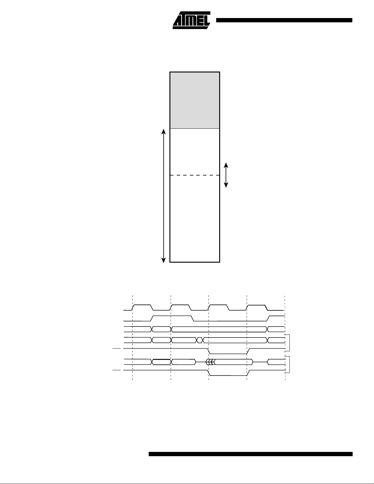
Figure 50. External memory with page select
Data Memory
$0000
Internal memory
$0460
Lower page
SRW01
SRW00
SRL[2..0]
External Memory
(0-63K x 8)
Upper page
SRW11
SRW10
$FFFF
Figure 51. External Data Memory Cycles without Wait State (SRWn1 = 0 and SRWn0 =0)
T1 T2 T3
System Clock Ø
ALE
Address [15..8]
Data / Address [7..0]
WR
Data / Address [7..0]
RD
Prev. addr.
Prev. data
Prev. data
XX
XX
XX
Address
Address
XX
Address
Data
Data
T4
XX
XX
Write
XX
Read
Note: SRWn1 = SRW11 (upper page) or SRW01 (lower page), SRWn0 = SRW10 (upper page) or SRW00 (lower page)
The ALE pulse in period T4 is only present if the next instruction accesses the RAM (internal or external). The Data and
Address will only change in T4 if ALE is present (the next instruction accesses the RAM).
74
ATmega161(L)
Page 75

Figure 52. External Data Memory Cycles with SRWn1 = 0 and SRWn0 = 1
ATmega161(L)
T4
T5
XX
XX
Write
XX
Read
System Clock Ø
ALE
Address [15..8]
Data / Address [7..0]
WR
Data / Address [7..0]
RD
Prev. addr.
Prev. data
Prev. data
T1 T2 T3
XX
XX
XX
Address
Address
XX
Address
Data
Data
Note: SRWn1 = SRW11 (upper page) or SRW01 (lower page), SRWn0 = SRW10 (upper page) or SRW00 (lower page)
The ALE pulse in period T5 is only present if the next instruction accesses the RAM (internal or external). The Data and
Address will only change in T5 if ALE is present (the next instruction accesses the RAM).
Figure 53. External Data Memory Cycles with SRWn1 = 1 and SRWn0 = 0
T4
T5
T6
XX
XX
XX
System Clock Ø
ALE
Address [15..8]
Data / Address [7..0]
WR
Data / Address [7..0]
RD
Prev. addr.
Prev. data
Prev. data
T1 T2 T3
XX
XX
XX
Address
Address
XX
Address
Data
Data
Write
Read
Note: SRWn1 = SRW11 (upper page) or SRW01 (lower page), SRWn0 = SRW10 (upper page) or SRW00 (lower page)
The ALE pulse in period T6 is only present if the next instruction accesses the RAM (internal or external). The Data and
Address will only change in T6 if ALE is present (the next instruction accesses the RAM).
Figure 54. External Data Memory Cycles with SRWn1 = 1 and SRWn0 = 1
T4
T5
System Clock Ø
ALE
Address [15..8]
Data / Address [7..0]
WR
Data / Address [7..0]
RD
Prev. addr.
Prev. data
Prev. data
T1 T2 T3
XX
XX
XX
Address
Address
XX
Address
Data
Data
Note: SRWn1 = SRW11 (upper page) or SRW01 (lower page), SRWn0 = SRW10 (upper page) or SRW00 (lower page)
The ALE pulse in period T7 is only present if the next instruction accesses the RAM (internal or external). The Data and
Address will only change in T7 if ALE is present (the next instruction accesses the RAM).
T6
T7
XX
XX
Write
XX
Read
75
Page 76

Using the External Memory Interface
The interface consists of:
• Port A: Multiplexed low-order address bus and data bus
• Port C: High-order address bus
• The ALE-pin: Address latch enable
• The R D
The external memory interface is enabled by setting the SRE – External SRAM enable bit of the MCUCR – MCU control
register, and will over-ride the setting of the data direction regist er DDRA, DDRD and DDRE. Whe n the SRE bit is cleared
(zero), the external memory interface is disabled, and the normal pin and data direction settings are used. When SRE is
low, the address space above the internal SRAM boundary is not mapped into the internal SRAM, as in AVR parts not having external memory interface.
When ALE goes from high to low, there is a valid address on Port A. ALE is low during a data transfer. RD
active when accessing the external memory only.
When the external m emory i nterfa ce is enable d, the AL E sig nal ma y have shor t puls es when access ing the int ernal RAM ,
but the ALE signal is stable when accessing the external memory.
Figure 55 sketches how to connect an external SRAM to the AVR using 8 latches which are transparent when G is high.
Figure 55. External SRAM connected to the AVR
and WR-pin: Read and write strobes.
and WR are
D[7:0]
Port A
ALE
DQ
G
AVR
Port C
RD
WR
For details in the timing for the SRAM interface, please refer to Figure 84 – Figure 87 and Table 49 – Table 56.
A[7:0]
SRAM
A[15:8]
RD
WR
I/O-Ports
All AVR ports have true Read-m odify-wri te functionali ty when used as ge neral digital I/O po rts. This mea ns that the direction of one port pin can be changed without unintentionally changing the direction of any other pin with the SBI and CBI
instructions. The same applies for changing drive value (if configured as output) or enabling/disabling of pull-up resistors (if
configured as input).
Port A
Port A is an 8-bit bi-directional I/O port.
Three I/O memory address locations are allocated for the Port A, one each for the Data Register – PORTA, $1B($3B), Data
Direction Register – DDRA, $1A($3A ) and the Por t A Input Pi ns – PINA, $1 9($39). Th e Port A In put Pins add ress is re ad
only, while the Data Register and the Data Direction Register are read/write.
All port pins have individually selectable pull-up resistors. The Port A output buffers can sink 20 mA and thus drive LED displays directly. When pins PA0 to PA7 are used as inputs and are externally pulled low, they will sour ce current if the
internal pull-up resistors are activated.
76
ATmega161(L)
Page 77

ATmega161(L)
The Port A pins have al terna te func tions relat ed to the o ptiona l extern al memo ry inter face . Port A can be c onfigu red to b e
the multiplexed low-order address/data bus during accesses to the external data memory. In this mode, Port A has internal
pull-up resistors.
When Port A is set to t he al ter na te fu nc tio n by the SRE – E xternal SRA M Enab le bit in the MC UCR – MCU Con trol R egi ster, the alternate settings override the data direction register.
Port A Data Register – PORTA
Bit 76543210
$1B ($3B) PORTA7 PORTA6 PORTA5 PORTA4 PORTA3 PORTA2 PORTA1 PORTA0 PORTA
Read/Write R/W R/W R/W R/W R/W R/W R/W R/W
Initial value 0 0 0 0 0 0 0 0
Port A Data Direction Register – DDRA
Bit 76543210
$1A ($3A) DDA7 DDA6 DDA5 DDA4 DDA3 DDA2 DDA1 DDA0 DDRA
Read/Write R/W R/W R/W R/W R/W R/W R/W R/W
Initial value 0 0 0 0 0 0 0 0
Port A Input Pins Address – PINA
Bit 76543210
$19 ($39) PINA7 PINA6 PINA5 PINA4 PINA3 PINA2 PINA1 PINA0 PINA
Read/Write RRRRRRRR
Initial value Hi-Z Hi-Z Hi-Z Hi-Z Hi-Z Hi-Z Hi-Z Hi-Z
The Port A In put Pi ns ad dress – PINA – is not a register, and this address enables access to the physical value on each
Port A pin. When reading PORTA the Port A Data Latch is read, and when reading PINA, the logical values present on the
pins are read.
Port A as General Digital I/O
All 8 pins in Port A have equal functionality when used as digital I/O pins.
PAn, General I/O pin: The DDAn bit in the DDRA regi ster sel ects the d irection of t his pin, i f DDA n is set (one ), PAn is c on-
figured as an output pi n. I f DDA n is c lear ed (z er o), P A n i s configured as an input pi n. If P O RTAn is s et (one) w hen the pi n
configured as a n in put p in, th e MO S pu ll-up resis tor i s ac tivated . To swi tch the pu ll-up res istor off, the P ORTAn has to b e
cleared (zero) or the pin has to be configured as an output pin. The Port A pins are tri-stated when a reset condition
becomes active, even if the clock is not running.
Table 28. DDAn Effects on Port A Pins
DDAn PORTAn I/O Pull-up Comment
0 0 Input No Tri-state (Hi-Z)
0 1 Input Yes PAn will source current if ext. pulled low.
1 0 Output No Push-pull Zero Output
1 1 Output No Push-pull One Output
n: 7,6…0, pin number.
Port A Schematics
Note that all port pins are synchronized. The synchronization latch is however, not shown in the figure.
77
Page 78

Figure 56. Port A Schematic Diagrams (Pins PA0 - PA7)
Port B
Port B is an 8-bit bi-directional I/O port.
Three I/O memory address locations are allocated for the Port B, one each for the Data Register – PORTB, $18($38), Data
Direction Register – DDRB, $17($37) and the Port B Input Pins – PINB, $16($36). The Port B Input Pins address is read
only, while the Data Register and the Data Direction Register are read/write.
All port pins have individually selectable pull-up resistors. The Port B output buffers can sink 20 mA and thus drive LED displays directly. When pins PB0 to PB7 are used as inputs and are externally pulled low, they will sour ce current if the
internal pull-up resistors are activated.
The Port B pins with alternate functions are shown in the following table:
Table 29. Port B Pins Alternate Functions
Port Pin Alternate Functions
PB0 OC0 (Timer/Counter 0 Compare match Output) /T0 (Timer/Counter 0 external counter input)
PB1 OC2 (Timer/Counter 2 Compare match Output) /T1 (Timer/Counter 1 external counter input)
PB2 RXD1 (UART1 input line) /AIN0 (Analog comparator positive input)
PB3 TXD1 (UART1 output line) /AIN1 (Analog comparator negative input)
PB4 SS
PB5 MOSI (SPI Bus Master Output/Slave Input)
PB6 MISO (SPI Bus Master Input/Slave Output)
PB7 SCK (SPI Bus Serial Clock)
(SPI Slave Select input)
78
ATmega161(L)
Page 79

ATmega161(L)
When the pins are used for the alternate function th e DDRB and POR TB register has to be set accordi ng to the alte rnate
function description.
Port B Data Register – PORTB
Bit 76543210
$18 ($38) PORTB7 PORTB6 PORTB5 PORTB4 PORTB3 PORTB2 PORTB1 PORTB0 PORTB
Read/Write R/W R/W R/W R/W R/W R/W R/W R/W
Initial value 0 0 0 0 0 0 0 0
Port B Data Direction Register – DDRB
Bit 76543210
$17 ($37) DDB7 DDB6 DDB5 DDB4 DDB3 DDB2 DDB1 DDB0 DDRB
Read/Write R/W R/W R/W R/W R/W R/W R/W R/W
Initial value 0 0 0 0 0 0 0 0
Port B Input Pins Address – PINB
Bit 76543210
$16 ($36) PINB7 PINB6 PINB5 PINB4 PINB3 PINB2 PINB1 PINB0 PINB
Read/Write RRRRRRRR
Initial value Hi-Z Hi-Z Hi-Z Hi-Z Hi-Z Hi-Z Hi-Z Hi-Z
The Port B In put Pi ns ad dress – PINB – is not a register, and this address enables access to the physical value on each
Port B pin. When reading PORTB, the Port B Data Latch is read, and when reading PINB, the logical values present on the
pins are read.
Port B as General Digital I/O
All 8 pins in Port B have equal functionality when used as digital I/O pins.
PBn, General I/O pin: The DDBn bit in the DDRB regi ster sel ects the d irection of t his pin, i f DDB n is set (one ), PBn is c on-
figured as an output pi n. I f DDB n is c lear ed (z er o), P B n i s configured as an input pi n. If P O RTBn is s et (one) w hen the pi n
configured as a n in put p in, th e MO S pu ll-up resis tor i s ac tivated . To swi tch the pu ll-up res istor off, the P ORTBn has to b e
cleared (zero) or the pin has to be configured as an output pin. The Port B pins are tri-stated when a reset condition
becomes active, even if the clock is not running
Table 30. DDBn Effects on Port B Pins
DDBn PORTBn I/O Pull-up Comment
0 0 Input No Tri-state (Hi-Z)
0 1 Input Yes PBn will source current if ext. pulled low.
1 0 Output No Push-pull Zero Output
1 1 Output No Push-pull One Output
n: 7,6…0, pin number.
79
Page 80

Alternate functions of Port B
The alternate pin configuration is as follows:
SCK - Port B, Bit 7
•
SCK: Master clock outpu t, sl av e cloc k in put pi n for SP I cha nne l. Wh en the SPI is en abled as a sla ve , this pin is conf igu re d
as an input regardless of the setting of DDB7. When the SPI is enabled as a master, the data direction of this pin is controlled by DDB7. When the pin is forced to be an input, the pull-up can still be controlled by the PORTB7 bit. See the
description of the SPI port for further details.
MISO - Port B, Bit 6
•
MISO: Master data input, slave data output pin for SPI channel. When the SPI is enabled as a master, this pin is configured
as an input regardless of the setting of DDB6. When the SPI is enabled as a slave, the data direction of this pin is controlled
by DDB6. When the pin is forced to be an input, the pull-up can still be controlled by the PORTB6 bit. See the description of
the SPI port for further details.
MOSI - Port B, Bit 5
•
MOSI: SPI Master data output, slave data input for SPI channel. When the SPI is enabled as a slave, this pin is configured
as an input regardless of the setting of DDB5. When the SPI is enabled as a master, the data direction of this pin is controlled by DDB5. When the pin is forced to be an input, the pull-up can still be controlled by the PORTB5 bit. See the
description of the SPI port for further details.
SS - Port B, Bit 4
•
SS: Slave port select inp ut. W hen the SP I is ena bl ed as a sl av e, th is pin is conf igured as an input regard le ss of the setting
of DDB5. As a slave, the SPI is activated when this pin is driven low. When the SPI is enabled as a master, the data direction of this pin is controlled by DDB 5. When the pin is forced to be an input, the pul l-up can still be contro lled by the
PORTB5 bit. See the description of the SPI port for further details.
TXD1/AIN1 - Port B, Bit 3
•
AIN1, Analog Comparator Negative Input. This pin also serves as the negative input of the on-chip analog comparator.
TXD1, Transmit Data (Data output pin for the UART1). When the UART1 transmitter is enabled, this pin is configured as an
output regardless of the value of DDRB3.
RXD1/AIN0 - Port B, Bit 2
•
AIN0, Analog Comparator Positive Input. This pin also serves as the positive input of the on-chip analog comparator.
RXD1, receive Data (Data input pin for the UART1). When the UART1 receiver is enabled this pin is configured as an input
regardless of the value of DDRB2. When the UART1 forces this pin to be an input, a logical one in PORTB2 will turn on the
internal pull-up.
OC2/T1 - Port B, Bit 1
•
T1, Timer/Counter1 counter source. See the “Timer/Counter1.” on page 45 for further details.
OC2, Output compare match output: The PB1 pin can serve as an external output when the Timer/Counter2 compare
matches. The PB1 pin has to be configured as an output (DDB1 set (one)) to serve this function. See “8-bit Timers/Counters T/C0 and T/C2” on page 37 for further details. The OC2 pin is also the output pin for the PWM mode timer
function.
OC0/T0 - Port B, Bit 0
•
T0: Timer/Counter0 counter source. See the “8-bit Timers/Counters T/C0 and T/C2” on page 37 further details.
OC0, Output compare match output: The PB0 pin can serve as an external output when the Timer/Counter0 compare
matches. The PB0 pin has to be configured as an output (DDB0 set (one)) to serve this function. See “8-bit Timers/Counters T/C0 and T /C2” on page 37 for further details, and how to enable the outp ut. The OC0 pin is also the outp ut
pin for the PWM mode timer function.
Port B Schematics
Note that all port pins are synchronized. The synchronization latches are however, not shown in the figures.
80
ATmega161(L)
Page 81
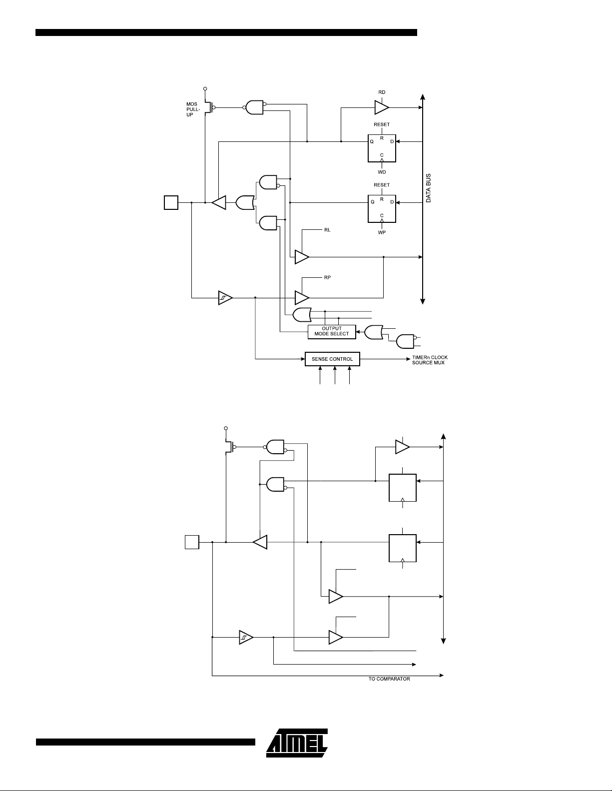
Figure 57. Port B Schematic Diagram (Pins PB0 and PB1)
ATmega161(L)
DDBn
PBn
WRITE PORTB
WP:
WRITE DDRB
WD:
READ PORTB LATCH
RL:
READ PORTB PIN
RP:
READ DDRB
RD:
n: 0,1
x: 0,2
Figure 58. Port B Schematic Diagram (Pin PB2)
MOS
PULLUP
PB2
CSn2
CSn1
CSn0
PORTBn
COMx0
COMx1
COMP. MATCH x
PWMx
FOCx
RD
RESET
D
Q
DDB2
C
WD
RESET
D
Q
PORTB2
C
RL
WP
DATA BUS
WP:
WRITE PORTB
WD:
WRITE DDRB
RL:
READ PORTB LATCH
RP:
READ PORTB PIN
RD:
READ DDRB
RXD1:
UART1 RECEIVE DATA
RXEN1:
UART1 RECEIVE ENABLE
AIN0: ANALOG COMPARATOR POSITIVE INPUT
RP
RXEN1
RXD1
AIN0
81
Page 82

Figure 59. Port B Schematic Diagram (Pin PB3)
MOS
PULLUP
PB3
WRITE PORTB
WP:
WRITE DDRB
WD:
READ PORTB LATCH
RL:
READ PORTB PIN
RP:
READ DDRB
RD:
UART1 TRANSMIT DATA
TXD1:
UART1 TRANSMIT ENABLE
TXEN1:
AIN1: ANALOG COMPARATOR NEGATIVE INPUT
RD
RESET
R
D
Q
DDB3
C
WD
RESET
R
Q
D
PORTB3
C
RL
RP
WP
DATA BUS
TXEN1
TXD1
AIN1
Figure 60. Port B Schematic Diagram (Pin PB4)
MOS
PULLUP
PB4
WRITE PORTB
WP:
WRITE DDRB
WD:
READ PORTB LATCH
RL:
READ PORTB PIN
RP:
READ DDRB
RD:
SPI MASTER ENABLE
MSTR:
SPI ENABLE
SPE:
RD
RESET
D
Q
DDB4
C
WD
RESET
D
Q
PORTB4
C
RL
RP
WP
DATA BUS
MSTR
SPE
SPI SS
82
ATmega161(L)
Page 83

Figure 61. Port B Schematic Diagram (Pin PB5)
MOS
PULLUP
PB5
WRITE PORTB
WP:
WRITE DDRB
WD:
READ PORTB LATCH
RL:
READ PORTB PIN
RP:
READ DDRB
RD:
SPI ENABLE
SPE:
MASTER SELECT
MSTR
ATmega161(L)
RD
RESET
R
D
Q
DDB5
C
WD
RESET
R
Q
D
PORTB5
C
RL
WP
RP
MSTR
SPE
SPI MASTER
OUT
DATA BUS
Figure 62. Port B Schematic Diagram (Pin PB6)
MOS
PULLUP
PB6
WRITE PORTB
WP:
WRITE DDRB
WD:
READ PORTB LATCH
RL:
READ PORTB PIN
RP:
READ DDRB
RD:
SPI ENABLE
SPE:
MASTER SELECT
MSTR
SPI SLAVE
IN
RD
RESET
R
D
Q
DDB6
C
WD
RESET
R
Q
D
PORTB6
C
RL
WP
RP
MSTR
SPE
SPI SLAVE
OUT
SPI MASTER
IN
DATA BUS
83
Page 84

Figure 63. Port B Schematic Diagram (Pin PB7)
MOS
PULLUP
PB7
WRITE PORTB
WP:
WRITE DDRB
WD:
READ PORTB LATCH
RL:
READ PORTB PIN
RP:
READ DDRB
RD:
SPI ENABLE
SPE:
MASTER SELECT
MSTR
RD
RESET
R
D
Q
DDB7
C
WD
RESET
R
Q
D
PORTB7
C
RL
WP
RP
MSTR
SPE
SPI ClLOCK
OUT
SPI CLOCK
IN
DATA BUS
Port C
Port C is an 8-bit bi-directional I/O port.
Three I/O memory address locations are allocated for the Port C, one each for the Data Register – PORTC, $15($35), Data
Direction Register – DDRC, $14($34) and the Port C Input Pins – PINC, $13($33). The Port C Input Pins addres s is read
only, while the Data Register and the Data Direction Register are read/write.
All port pins have individually selectable pull-up resistors. The Port C output buffers can sink 20 mA and thus drive LED displays directly. When pins PC0 to PC7 are used as inputs and are externally pulled low, they will source current if the
internal pull-up resistors are activated.
The Port C pins have alternate fun ction s related to the optiona l exter nal memo ry interfac e. Por t C can be configur ed to be
the high-order address byte during accesses to external data memory.
When Port C is set to the alternate function by the SRE – Extern a l SRA M En abl e – bit in the MCUCR – MCU Control Register, the alternate settings override the data direction register.
84
ATmega161(L)
Page 85

ATmega161(L)
Port C Data Register – PORTC
Bit 76543210
$15 ($35) PORTC7 PORTC6 PORTC5 PORTC4 PORTC3 PORTC2 PORTC1 PORTC0 PORTC
Read/Write R/W R/W R/W R/W R/W R/W R/W R/W
Initial value 0 0 0 0 0 0 0 0
Port C Data Direction Register – DDRC
Bit 76543210
$14 ($34) DDC7 DDC6 DDC5 DDC4 DDC3 DDC2 DDC1 DDC0 DDRC
Read/Write R/W R/W R/W R/W R/W R/W R/W R/W
Initial value 0 0 0 0 0 0 0 0
Port C Input Pins Address – PINC
Bit 76543210
$13 ($33) PINC7 PINC6 PINC5 PINC4 PINC3 PINC2 PINC1 PINC0 PINC
Read/Write RRRRRRRR
Initial value Hi-Z Hi-Z Hi-Z Hi-Z Hi-Z Hi-Z Hi-Z Hi-Z
The Port C Input Pins address – PINC – is not a register, and this address enables access to the physical value on each
Port C pin. When reading PORTC, the Port C Data Latch is read, and when reading PINC, the logical values present on the
pins are read.
Port C as General Digital I/O
All 8 pins in Port C have equal functionality when used as digital I/O pins.
PCn, General I/O pin: The DDCn bit in the DDRC register selects the direction of this pin, if DDCn is set (one), PCn is con-
figured as an output pin. If DDCn is cleared (zero), PCn i s confi gure d as an input pi n. If P ORTC n is set (one) when the pi n
configured as an input pin , the MOS pu ll-up re sistor is activate d. To swit ch the pull -up resist or off, PO RTCn has to b e
cleared (zero) or the pin has to b e configured as an output pin .The Port C pins are tri-s tated when a r eset condition
becomes active, even if the clock is not running.
Table 31. DDCn Effects on Port C Pins
DDCn PORTCn I/O Pull-up Comment
0 0 Input No Tri-state (Hi-Z)
0 1 Input Yes PCn will source current if ext. pulled low.
1 0 Output No Push-pull Zero Output
1 1 Output No Push-pull One Output
n: 7, 6,…0, pin number
Port C Schematics
Note that all port pins are synchronized. The synchronization latch is however, not shown in the figure.
85
Page 86
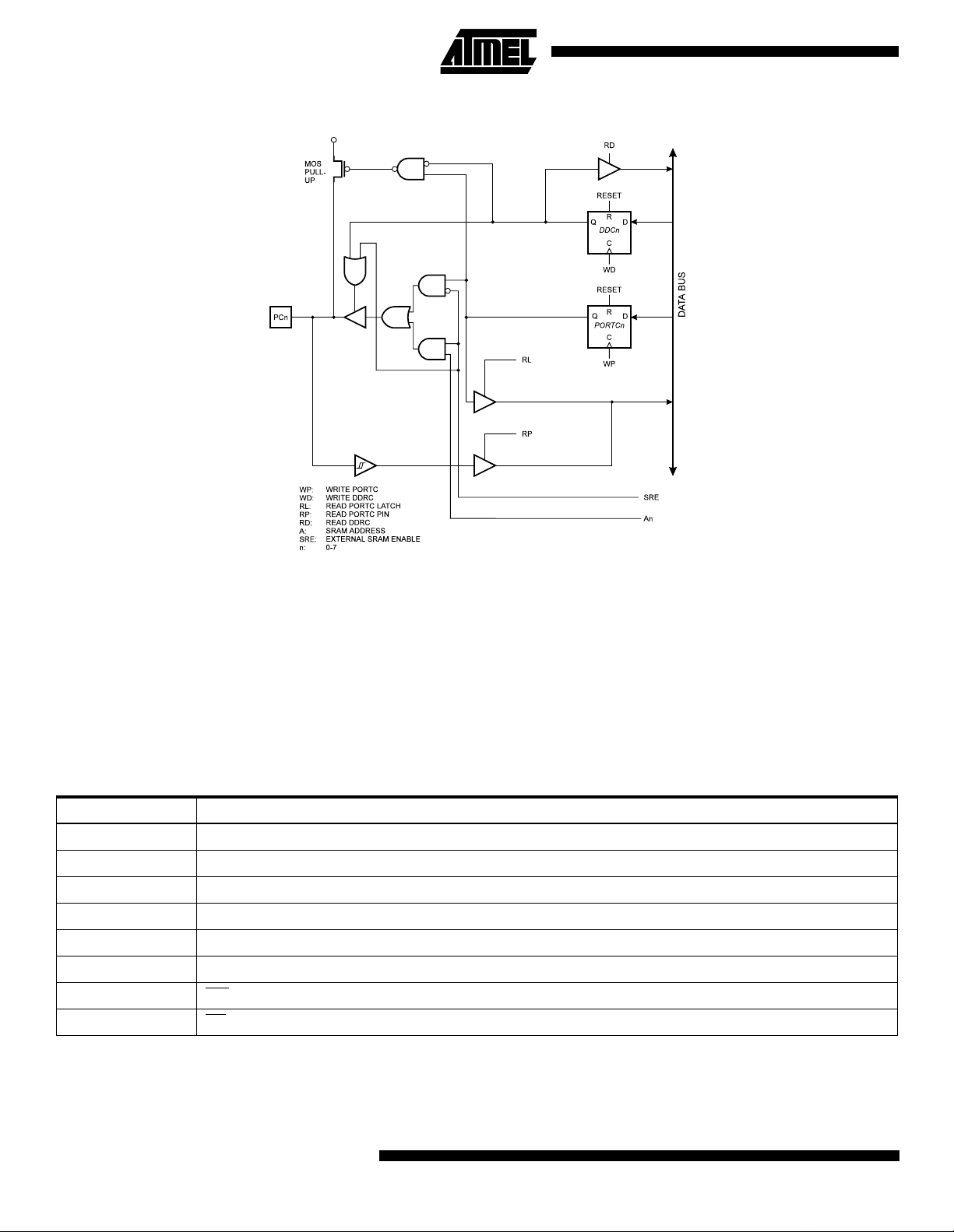
Figure 64. Port C Schematic Diagram (Pins PC0 - PC 7 )
Port D
Port D is an 8 bit bi-directional I/O port with internal pull-up resistors.
Three I/O address locations are allocated for the Port D, one each for the Data Register – PORTD, $12($32), Data
Direction Register – DDRD, $11($31) and the Port D Input Pins – PIND, $10($30). The Port D Input Pins address is read
only, while the Data Register and the Data Direction Register are read/write.
The Port D output buffers can sink 20 mA. As inputs, Port D pins that are externally pulled low will source current if the pullup resistors are activated.
Some Port D pins have alternate functions as shown in the following table:
Table 32. Port D Pins Alternate Functions
Port Pin Alternate Function
PD0 RXD0 (UART0 Input line)
PD1 TXD0 (UART0 Output line)
PD2 INT0 (External interrupt 0 input)
PD3 INT1 (External i nterrupt 1 input)
PD3 TOSC1 (RTC oscillator Timer/Counter 2)
PD5 TOSC2 (RTC oscillator Timer/Counter 2)/OC1A (Timer/Counter1 Output compareA match output)
PD6 WR
PD7 RD (Read strobe to external memory)
(Write strobe to external memory)
When the PD5 pin is used for the alternate func tion (OC1 A) the DDRD and PORTD regist er has to be s et acc ording to th e
alternate function description.
86
ATmega161(L)
Page 87

ATmega161(L)
Port D Data Register – PORTD
Bit 76543210
$12 ($32) PORTD7 PORTD6 PORTD5 PORTD4 PORTD3 PORTD2 PORTD1 PORTD0 PORTD
Read/Write R/W R/W R/W R/W R/W R/W R/W R/W
Initial value 0 0 0 0 0 0 0 0
Port D Data Direction Register – DDRD
Bit 76543210
$11 ($31) DDD7 DDD6 DDD5 DDD4 DDD3 DDD2 DDD1 DDD0 DDRD
Read/Write R/W R/W R/W R/W R/W R/W R/W R/W
Initial value 0 0 0 0 0 0 0 0
Port D Input Pins Address – PIND
Bit 76543210
$10 ($30) PIND7 PIND6 PIND5 PIND4 PIND3 PIND2 PIND1 PIND0 PIND
Read/Write RRRRRRRR
Initial value Hi-Z Hi-Z Hi-Z Hi-Z Hi-Z Hi-Z Hi-Z Hi-Z
The Port D Input Pins address – PIND – is not a register, and this address enables access to the physical value on each
Port D pin. When reading PORTD, the Port D Data Latch is read, and when reading PIND, the logical values present on the
pins are read.
Port D as General Digital I/O
PDn, General I/O pin: The DDDn bit in the DDRD register selects the direction of this pin. If DDDn is set (one), PDn is configured as an output pin. If DDDn is cleared (zero ), PDn is configured as an input pin. If POR TDn is set (one) when
configured as an input pi n the MOS pull-up resist or is acti vated. To switc h the pul l-up res istor of f, the PORT Dn has to be
cleared (zero) or the pin has to be configured as an output pin. The Port D pins ar e tri-stated when a reset condition
becomes active, even if the clock is not running.
Table 33. DDDn Bits on Port D Pins
DDDn PORTDn I/O Pull-up Comment
0 0 Input No Tri-state (Hi-Z)
0 1 Input Yes PDn will source current if ext. pulled low.
1 0 Output No Push-pull Zero Output
1 1 Output No Push-pull One Output
n: 7,6…0, pin number.
Alternate functions of Port D
RD - Port D, Bit 7
•
RD is the external data memory read control strobe.
WR - Port D, Bit 6
•
WR is the external data memory write control strobe.
•
OC1 - Port D, Bit 5
OC1, Output compare match output: The PD5 pin can serve as an external output when the Timer/Counter1 compare
matches. The PD5 pin has to be configured as an output (DDD5 set (one)) to serve this function. See “Timer/Counter1.” on
page 45 for further details, and how to enable the output. The OC1 pin is also the output pin for the PWM mode timer
function.
87
Page 88

TOSC1/TOSC2 - Port D, Bit 5 and 4
•
When the AS2 bit in ASSR is set (one) to enable asynchronous clocking of Timer/Counter2, pins PD5 and PD4 are disconnected from the port. In this mode, a crystal oscillator is connected to the pins, and the pins can not be used as I/O pins.
•
INT1 - Port D, Bit 3
INT1, External Interrupt source 1: The PD3 pin can serve as an external interrupt source to the MCU. See “MCU Control
Register – MCUCR” on page 32 for further details.
INT0 - Port D, Bit 2
•
INT0, External Interrupt source 0: The PD2 pin can serve as an external interrupt source to the MCU. See “MCU Control
Register – MCUCR” on page 32 for further details.
•
TXD0 - Port D, Bit 1
Transmit Data (Data output pin for the UART0). When the UART0 transmitter is enabled, this pin is configured as an output
regardless of the value of DDRD1.
•
RXD0 - Port D, Bit 0
Receive Data (Data input pin for the UART0). When the UART receiver is enabled this pin is configured as an input regardless of the value of DDRD0. When the UART0 forces this pin to be an input, a logical one in PORTD0 will turn on the
internal pull-up.
Port D Schematics
Note that all port pins are synchronized. The synchronization latches are however, not shown in the figures.
Figure 65. Port D Schematic Diagram (Pin PD0)
RD
MOS
PULLUP
RESET
PD0
WP:
WRITE PORTD
WD:
WRITE DDRD
RL:
READ PORTD LATCH
RP:
READ PORTD PIN
RD:
READ DDRD
RXD0:
UART0 RECEIVE DATA
RXEN0:
UART0 RECEIVE ENABLE
D
Q
DDD0
C
WD
RESET
D
Q
PORTD0
C
RL
RP
WP
RXEN0
RXD0
DATA BUS
88
ATmega161(L)
Page 89

Figure 66. Port D Schematic Diagram (Pin PD1)
MOS
PULLUP
PD1
WP:
WRITE PORTD
WD:
WRITE DDRD
RL:
READ PORTD LATCH
RP:
READ PORTD PIN
RD:
READ DDRD
TXD0:
UART0 TRANSMIT DATA
TXEN0:
UART0 TRANSMIT ENABLE
ATmega161(L)
RD
RESET
R
D
Q
DDD1
C
WD
RESET
R
Q
D
PORTD1
C
RL
RP
WP
DATA BUS
TXEN0
TXD0
Figure 67. Port D Schematic Diagram (Pins PD2 and PD3)
WP:
WRITE PORTD
WD:
WRITE DDRD
RL:
READ PORTD LATCH
RP:
READ PORTD PIN
RD:
READ DDRD
n:
2, 3
m:
0, 1
89
Page 90

Figure 68. Port D Schematic Diagram (Pin PD4)
MOS
PULLUP
PD4
WP:
WRITE PORTD
WD:
WRITE DDRD
RL:
READ PORTD LATCH
RP:
READ PORTD PIN
RD:
READ DDRD
AS2:
ASYNCH SELECT T/C2
Figure 69. Port D Schematic Diagram (Pin PD5)
RD
RESET
R
D
Q
DDD4
C
WD
RESET
R
D
Q
PORTD4
C
RL
RP
WP
AS2
T/C2 OSC
AMP INPUT
DATA BUS
90
WP:
WRITE PORTD
WD:
WRITE DDRD
RL:
READ PORTD LATCH
RP:
READ PORTD PIN
RD:
READ DDRD
AS2
ASYNCH SELECT T/C2
ATmega161(L)
COMP. MATCH 1A
PWM10
PWM11
FOC1A
Page 91

Figure 70. Port D Schematic Diagram (Pin PD6)
WP:
WRITE PORTD
WD:
WRITE DDRD
RL:
READ PORTD LATCH
RP:
READ PORTD PIN
RD:
READ DDRD
WE:
WRITE ENABLE
SRE:
EXTERNAL SRAM ENABLE
ATmega161(L)
Figure 71. Port D Schematic Diagram (Pin PD7)
WP:
WRITE PORTD
WD:
WRITE DDRD
RL:
READ PORTD LATCH
RP:
READ PORTD PIN
RD:
READ DDRD
RE:
READ ENABLE
SRE:
EXTERNAL SRAM ENABLE
91
Page 92

Port E
Port E is a 3 bit bi-directional I/O port with internal pull-up resistors.
Three I/O address lo cations ar e alloca ted for the P ort E, one each for the Data Reg ister – POR TE, $07($2 7), Data Direc -
tion Register – DDRE, $06($26) and the Port E Input Pins – PINE, $05($25). The Port E Input Pins address is read only,
while the Data Register and the Data Direction Register are read/write.
The Port E output buffers can sink 20 mA. As inputs, Port E pins that are externally pulled low will source current if the pullup resistors are activated.
Port E pins have alternate functions as shown in the following table:
Table 34. Port E Pins Alternate Functions
Port Pin Alternate Function
PE0 ICP (Input Capture Pin Timer/Counter1)/INT2 (External Interrupt 2 input)
PE1 OC1B (Timer/Counter1 Output CompareB match output)
PE2 ALE (Address Latch Enable, External Memory)
When the PE1 pin is used for the alternate function the DDRE and PORTE register has to be set according to the alternate
function description.
Port E Data Register – PORTE
Bit 76543210
$07 ($27) - - - - - PORTE2 PORTE1 PORTE0 PORTE
Read/Write R R R R R R/W R/W R/W
Initial value 0 0 0 0 0 0 0 0
Port E Data Direction Register – DDRE
Bit 76543210
$06 ($26) - - - - - DDE2 DDE1 DDE0 DDRE
Read/Write R R R R R R/W R/W R/W
Initial value 0 0 0 0 0 0 0 0
Port E Input Pins Address – PINE
Bit 76543210
$05 ($25) - - - - - PINE2 PINE1 PINE0 PINE
Read/Write RRRRRRRR
Initial value 0 0 0 0 0 Hi-Z Hi-Z Hi-Z
The Port E In put Pi ns ad dress – PINE – is not a register, and this address enables access to the physical value on each
Port E pin. When reading PORTE, the Port E Data Latch is read, and when reading PINE, the logical values present on the
pins are read.
Port E as General Digital I/O
PEn, General I/O pin: The DDEn bit in the DDRE register sel ects th e di rection o f this pi n. If DDE n is set (o ne), PEn i s configured as an out put pin. If DDEn is cleared (zer o), PEn is confi gured as an in put pin. If POR TEn is set (one ) when
configured as an input pin the MOS pull-up resistor is activated. To switch the pull-up resistor off the PORTEn has to be
cleared (zero) or t he pin ha s to be co nfigured as an output pin.T he Port E pi ns are tri-s tated when a r eset condi tion
becomes active, even if the clock is not running.
92
ATmega161(L)
Page 93

ATmega161(L)
Table 35. DDEn Bits on Port E Pins
DDEn PORTEn I/O Pull-up Comment
0 0 Input No Tri-state (Hi-Z)
0 1 Input Yes PEn will source current if ext. pulled low.
1 0 Output No Push-pull Zero Output
1 1 Output No Push-pull One Output
n: 2,1,0, pin number.
Alternate functions of Port E
OC1B - Port E, Bit 2
•
OC1B, Output compare match output: The PE2 p in can serve as an external output when the Timer/Counter1 c ompare
matches. The PE2 pin has to be configured as an output (DDE2 set (one)) to serve this function. See “Timer/Counter1.” on
page 45 for further details. The OC1B pin is also the output pin for the PWM mode timer function.
ALE - Port E, Bit 1
•
ALE: When the External Memory is enabled, the PE1 pin serves as the Dress Latch Enable. Note that enabling of External
Memory will override both the direction and port value. Se e “Interface to exter nal memory” on page 72 for a detailed
description.
ICP/INT2 - Port E, Bit 0
•
ICP, input capture pin: The P E0 p in c an serv e as the i npu t ca ptur e sour c e for T im er/Cou nter 1. See page 49 for a detailed
description.
INT2, External Interrupt source 2: The PE0 pin can serve as an external interrupt source to the MCU. See “Extended MCU
Control Register – EMCUCR” on page 33 for further details.
Port E Schemati cs
Figure 72. Port E Schematic Diagram (Pin PE0)
MOS
PULLUP
PE0
WRITE PORTE
WP:
WRITE DDRE
WD:
READ PORTE LATCH
RL:
READ PORTE PIN
RP:
READ DDRE
RD:
COMPARATOR IC ENABLE
ACIC:
COMPARATOR OUTPUT
ACO:
RD
RESET
R
Q
DDE0
C
WD
RESET
R
Q
PORTE0
C
RL
RP
0
NOISE CANCELER EDGE SELECT ICF1
1
ICNC1 ICES1
WP
D
ACIC
ACO
DATA BUS
D
ISC2
'1'
PORTE0
C
R
DQ
INT2
HW CLEAR
SW CLEAR
93
Page 94

Figure 73. Port E Schematic Diagram (Pin PE1)
MOS
PULLUP
PE1
WRITE PORTE
WP:
WRITE DDRE
WD:
READ PORTE LATCH
RL:
READ PORTE PIN
RP:
READ DDRE
RD:
XRAM ENABLE
SRE:
ALE: ALE PULSE FROM XRAM
RL
RP
RD
RESET
Q
DDE1
WD
RESET
Q
PORTE1
WP
SRE
ALE
R
D
C
R
D
C
DATA BUS
Figure 74. Port E Schematic Diagram (Pin PE2
PE2
WRITE PORTE
WP:
WRITE DDRE
WD:
READ PORTE LATCH
RL:
READ PORTE PIN
RP:
READ DDRE
RD:
DDE2
PORTE2
COM1B0
COM1B1
COMP. MATCH 1B
PWM10
PWM11
FOC1B
94
ATmega161(L)
Page 95

ATmega161(L)
Memory Programming
Boot Loader Support
The ATmega161 provides a mechanism for downloading and uploading program code by the MCU itself. This feature
allows flexible application software updates, controlled by the MCU using a Flash-resident Boot Loader program.
The ATmega161 FLASH memory is organized in two main sections;
1. The Application code section (address $0000 - $1DFF)
2. The Boot Loader section/Boot block (address $1E00 - $1FFF)
Figure 75. Memory sections
Program Memory
$0000
Application Code section
(7.5K x 16)
$1DFF
Boot Loader section
(512 x 16)
Boot Loader progra m can use a ny avail able data in terfac e and asso ciate d protoc ol, su ch as UART seria l bus in terfac e, to
input or output program code, and write (program) that code into the Flash memory, or read the code from the program
memory.
The program Flash me mory is divi ded into pag es that con tai ns 128 byt es each. T he Boo t Lo ader FLA SH sec ti on o cc up ies
8 pages from $1E00 to $1FFF by 16 bit words.
$1E00
$1FFF
95
Page 96
The Store Program Memory (SPM) ins truction can access the e ntire FLASH, but it can only be exec uted from the Bo ot
Loader FLASH sectio n. If no Boot Loader capab ility i s neede d, the entire FLASH is ava ilable for appl icatio n code . The
ATmega161 has two separate sets of Boot Lock Bits which can be set independently. This gives the user a unique flexibility
to select different levels of protection. The user can select:
To protect the entire FLASH from a software update by the Boot Loader Program.
•
• To only protect the Boot Loader section from a software update by the Boot Loader Program.
• To only protect the Application code section from a software update by the Boot Loader Program.
• Allowing software update in the entire FLASH
See Table 36 and Table 37 for further details. The Boot Loc k bits can be set in software and in Serial or Parallel
Programming mode, but they can only be cleared by a chip erase command.
Table 36. Boot Lock Bit0 Protection modes (Application section)
BLB0 mode BLB01 BLB02 Protection
1 1 1 No restrictions for SPM, LPM in the Application code section (address $0000 - $1DFF)
2 0 1 It is not allowed to update the Application code section (address $0000 - $1DFF) by SPM.
3 0 0 LPM read and SPM write prohibited in the Application code section (address $0000 - $1DFF)
410
Note: ’1’ means unprogrammed, ‘0’ means programmed
It is not allowed to read progra m code loca ted in the Applic ation code section (ad dress $0000 $1DFF) by LPM
Table 37. Boot Lock Bit1 Protection modes (Boot Loader section)
BLB1 mode BLB11 BLB12 Protection
1 1 1 No restrictions for SPM, LPM in the Boot Loader section (address $1E00 - $1FFF)
2 0 1 It is not allowed to update the Boot Loader section (address $1E00 - $1FFF) by SPM
3 0 0 LPM and SPM prohibited in the Boot Loader section (address $1E00 - $1FFF)
410
Note: ’1’ means unprogrammed, ‘0’ means programmed
It is not allowed to read program code located in the Boot Loader section (address $1E00 $1FFF) by LPM
Entering the Boot Loader Program
Entering the Boot Loader tak es pla ce by a jump or cal l from the application program . Th is may be initiated by some trigger
such as a command received via UART or SPI interface. Alternatively, the Boot Reset Fuse (BOOTRST) can be programmed so that the res et vecto r is pointi ng to addres s $1E00 aft er a reset. In this cas e, the Boot Lo ader is start ed after
the reset. After the application code is loaded, the program can start executing the application code. Note that the fuses
cannot be changed by the MCU itself. This means that once the Boot Reset Fuse is programmed, the Reset Vec tor will
always point to the Boot Loader Reset and t he fu se ca n only be change d throu gh the s erial or p arall el progr ammi ng interface. The BOOTRST fuse c an al so be l oc ked by p ro gra mm in g LB 1. When LB1 is programmed it i s not poss ibl e to ch ang e
the BOOTRST fuse unless a chip erase command is performed first.
Table 38. Boot Reset Fuse, BOOTRST
BOOTRST Reset Address
1 Reset Vector = Application reset (address $0000)
0 Reset Vector = Boot Loader reset (address $1E00)
Note: ’1’ means unprogrammed, ‘0’ means programmed
96
ATmega161(L)
Page 97

ATmega161(L)
Capabilities of the Boot Loader
The program code within the Boot Loader section has the capability to read from and write into the entire FLASH, including
the Boot Loader Memory . This all ows the use r to upd ate b oth th e Application code and the Bo ot Loader code that handles
the software update. The Boot Loader can thus even modify itself, and it can also erase itself from the code if the feature is
not needed anymore. S pecial care must be taken i f the user al lo ws th e Bo ot Lo ader s ec tio n to be upda ted b y le av in g Bo ot
Lock bit11 unprogrammed. An accidental write to the Boot Loader itself can corrupt the entire Boot Loader, and further software updates might be impossible. If it is not needed to change the Boot Loader software itself, it is recommended to
program the Boot Lock bit11 to protect the Boot Loader software from software changes.
Self-programming the Flash
Programming of the Flash is executed one page at a time. The Flash page must be erased first for correct programming.
The general Write Lock ( Lock B it 2) do es no t cont rol the progr ammi ng of the Flas h mem ory by SPM i nstru ction . Simil arly,
the Read/Write Lock (Lock Bit 1) does not control reading nor writing by LPM/SPM, if it is attempted.
The program mem ory c an o nly be u pdate d pag e by p age, not w ord by w ord. One p age i s 1 28 byte s ( 64 wo rds) . The program memory will be modified by first performing page erase , then filling the te mporary page bu ffer one word at a time
using SPM, and th en ex ecuting page wri te. If only part of the pag e needs to be chan ged, the other p arts mus t be stor ed
(for example in the te mporary pa ge buffer) be fore the erase, a nd then be rew ritten. The te mporary pa ge buffer can be
accessed in a r andom sequen ce. The CPU i s hal ted bo th durin g page eras e and during page w rite. It is es senti al that th e
page address used in both the page erase and page write operation is addressing the same page.
Setting the Boot Loader Lock Bits by SPM
•
To set the Boot Loader Lock bits, writ e the desi red dat a to R0, write "10 01" to SP MCR and ex ecute SPM with in four clo ck
cycles after writing SPMCR. The only accessible lock bits are the Boot Lock bits that may prevent the Application and Boot
Loader section from any software update by the MCU. See Table 36 and Table 37 how the different settings of the Boot
Loader Bits affect the FLASH access.
Bit 76543210
- - BLB12 BLB11 BLB02 BLB01 - - R0
If bit5 - bit2 in R0 is cleared (zero), the corresponding Boot Lock Bit will be programmed if a SPM instruction is executed
within four cycles after BLBSET and SPMEN are set in SPMCR.
Performing Page Erase by SPM
•
To execute page erase, set up the address in the Z pointer, write "0011" to SP MCR and execute SPM within four clock
cycles after writing SPMCR. The data in R1 and R0 are ignored. The page address must be written to Z13:Z7. Other bits in
the Z pointer will be ignored during this operation.
Fill the temporary buffer
•
To write an instruction word, set up the address in the Z pointer and data in R1:R0, write "0001" to SPMCR and execute
SPM within four clock cycles after writing SPMCR. The content of Z6:Z1 is used to address the data in the temporary
buffer. Z13:Z7 must point to the page that is supposed to be written.
Perform a Page Write
•
To execute page wr ite, set up the a ddress i n the Z pointer, w rite "010 1" to S PMCR an d execute SPM withi n four c lock
cycles after writing SP MCR. The data in R1 and R0 ar e ignored . The pa ge address must be written to Z13:Z7 . During this
operation, Z6:Z0 must be zero to ensure that the page is written correctly.
97
Page 98

Addressing the FLASH During Self-programming
The Z pointer is used to address the SPM commands.
Bit 151413121110 9 8
$1F ($1F) Z15 Z14 Z13 Z12 Z11 Z10 Z9 Z8 ZH
$1E ($1E) Z7 Z6 Z5 Z4 Z3 Z2 Z1 Z0 ZL
76543210
Z15:Z14 always ignored
Z13:Z7 page select, for page erase, page write
Z6:Z1 word select, for filling temp buffer (must be zero during page write operation)
Z0 should be zero for all SPM commands, byte select for the LPM instruction.
The only operation tha t does not use the Z pointer is Setting the Boot Loader Lock B its. The co ntent of the Z pointer is
ignored and will have no effect on the operation.
Note that the page erase and page write operation is addressed independently. Therefore it is of major importance that the
Boot Loader software addresses the same page in both the page erase and page write operation.
The LPM instruc ti on doe s al so u se th e Z pointer to store the ad dres s. S inc e thi s i ns tr uct ion d oes a ddr ess th e FL AS H by te
by byte, also the LSB (bit Z0) of the Z pointer is used. See page 16 for a detailed description.
Accidental writing into Flash program by the SPM instruction is prevented by setting up a "SPM enable time window". All
accesses are e xecu ted by fir st s ett ing I/O bits, and the n e xe cuting SPM within fou r c lo ck c ycl es . The I/O register that c ontrols the SPM accesses is defined as follows:
Store Program Memory Control Register – SPMCR
The Store Program Memory Control Register contains the control bits needed to control the programming of the FLASH
from internal code executio n.
Bit 76543210
$37 ($57) - - BLBSET PGWRT PGERS SPMEN SPMCR
Read/Write R R R R R/W R/W R/W R/W
Initial value 0 0 0 0 0 0 0 0
Bit 7..4 - Res: Reserved Bits
•
These bits are reserved bits in the ATmega161 and always read as zero.
•
Bit 3 - BLBSET: Boot Lock Bit set
If this bit is set at the same time as SPMEN, the next SPM instruction within four clock cycles sets Boot Lock bits, according
to the data in R0. The data in R1 and the address in the Z pointer are ignored. The BLBSET bit will auto-clear upon completion of lock bit set, or if no SPM instruction is executed within four clock cycles. The CPU is halted during lock bit setting.
Only a chip erase can clear the Lock Bits.
An LPM instruction within four cycles after BLBSET and SPMEN are set in the SPMCR register, will put either the Lock-bits
or the Fuse-bits (de pen di ng o d the Z 0 i n the Z-p oi nter) in to th e de stination register . See “Rea di ng th e F use- an d Lo ck B its
from Software” on page 99 for details.
Bit 2 - PGWRT: Page write
•
If this bit is set at the same time as SPMEN, the next SPM instruction within four clock cycles executes page write, with the
data stored in the te mpora ry buffer . The p age ad dres s is tak en fr om the high part of th e Z p ointer . The da ta in R1 and R0
are ignored. The PGWRT bit will auto-clear upon completion of a page write, or if no SPM instruction is executed within four
clock cycles. The CPU is halted during the entire page write operation.
Bit 1 - PGERS: Page Erase
•
If this bit is set at the same time as SPMEN, the next SPM instruction within four clock cycles executes page erase. The
page address is taken from the high part of the Z pointer. The data in R1 and R0 are ignored. The PGERS bit will auto-clear
upon completion of a page erase, or if no SPM instruction is executed within four clock cycles. The CPU is halted during the
entire page erase operation.
98
ATmega161(L)
Page 99

ATmega161(L)
Bit 0 - SPMEN: Store Program Memory Enable
•
This bit enables the SPM instruction for the next four clock cycles. If set together with either BLBSET, PGWRT or PGERS,
the following SPM ins truc ti on wi ll ha ve a s pe cial mea ning, see description abo ve . If only SPMEN is set, the following SPM
instruction will s tore t he value in R1:R0 in th e te mpo r ar y pag e b uffe r add re ssed by t he Z po int er . T he LS B of the Z pointer
is ignored. The SPMEN bit will auto-clear upon completion of an SPM instruction, or if no SPM instruction is executed
within four clock cycles.
Writing any other combination that "1001", "0101", "0011" or "0001" in the lower four bits, or writing to the I/O register when
any bits are set, will have no effect.
EEPROM Write Prevents Writing to SPMCR
Note that an EEPROM wri te operati on will block a ll so ftware pro gramm ing to Fl ash. Re ading t he Fuses an d Lo ckbits f rom
software will also b e p reve nted dur i ng t he E EPR OM write operation. It i s re co mm ende d th at th e u ser che ck s the sta tus bit
(EEWE) in the EECR register and verifies that the bit is cleared before writing to the SPMCR register.
Reading the Fuse- and Lock Bits from Software
It is possible to read both the Fuse and Lock bits fr om softw are. To read the Lo ck bits, loa d the Z-po inter with $000 1 and
set the BLBSET and SPM EN bits i n SPMC R. If an LP M instr uction is exec uted wi thin three CPU cyc les af ter the BLB SET
and SPMEN bits are se t in SP MCR, the Lo ck bi ts will be writte n to the de stina tion regi ster. The BLBS ET and S PMEN b its
will auto-clear upon completion of r eading the Lock bits o r if no LPM/SPM ins truction is e xecuted within three/four CPU
cycles. When BLBSET and SPMEN are cleared, LPM will work as described in “Constant Addressing Using the LPM
Instruction” on page 16 and in the Instruction set Manual.
Bit 76543210
- - BLB12 BLB11 BLB02 BLB01 LB2 LB1 R0/Rd
The algorithm for reading the Fuse bits is similar to the one described above for reading the Lock bits. But when reading the
Fuse bits, load $0000 in the Z-poi nter. W hen an LPM instr uction is executed within three cy cles after the BLBS ET an d
SPMEN bits are set in the SPMCR, the Fuse-bits can be read in the destination register as shown below.
Bit 76543210
- BOOTRST SPIEN BODLEVEL BODEN CKSEL[2] CKSEL[1] CKSEL[0] R0/Rd
Fuse- and lock bits that are programmed, will be read as zero.
99
Page 100

Program Memory Lock Bits
The ATmega161 MCU provides six Lock bits which can be left unprogrammed (‘1’) or can be programmed (‘0’) to obtain
the additional features listed in Table 39. The Lock bits can only be erased to ‘1’ with the Chip Erase command.
Table 39. Lock Bit Protection Modes
Memory Lock Bits Protection Type
LB mode LB1 LB2
1 1 1 No memory lock features enabled
201
300
BLB0 mode BLB01 BLB02
111
2 0 1 SPM prohibited in the Application code section (address $0000 - $1DFF)
3 0 0 LPM and SPM prohibited in the Application code section (address $0000 - $1DFF)
4 1 0 LPM prohibited in the Application code section (address $0000 - $1DFF)
BLB1 mode BLB11 BLB12
1 1 1 No memory lock features on SPM and LPM in Boot Loader section (address $1E00 - $1FFF).
2 0 1 SPM prohibited in the Boot Loader section (address $1E00 - $1FFF)
3 0 0 LPM and SPM prohibited in the Boot Loader section (address $1E00 - $1FFF)
4 1 0 LPM prohibited in the Boot Loader section (address $1E00 - $1FFF)
Note: 1. Program the Fuse bits before programming the Lock bits.
Further programming of the Flash and EEPROM is disabled in parallel and serial programming
mode. The Fuse bits are locked in both serial and parallel programming mode.
Further programming and verification of the FLASH and EEPROM is disabled in parallel and
serial programming mode. The Fuse bits are locked in both serial and parallel programming
(1)
mode.
No memory lock features on SPM and LPM in Application code section (address $0000 $1DFF).
.
(1)
Fuse Bits
The ATmega161 has seven fuse bits, BOOTRST, SPIEN, BODLEVEL, BODEN and CKSEL [2:0].
• When BOOTRST is programmed (‘0’), the reset vector is set to address $1E00 which is the first address location in the
Boot Loader section of the FLASH. If the BOOTRST is unprogrammed (‘1’), the reset vector is set to address $0000.
Default value is unprogrammed (‘1’).
• When the SPIEN Fuse is programmed (‘0’), Serial Program and Data Downloading is enabled. Default value is
programmed (‘0’). The SPIEN Fuse is not accessible in serial programming mode.
• The BODLEVEL Fuse selects the Brown-out Detection Level and changes the Start-up times. See “Brown-out Detection”
on page 27. Default value is unprogrammed (‘1’).
• When the BODEN Fuse is programmed (‘0’), the Brown-out Detector is enabled. See “Brown-out Detection” on page 27.
Default value is unprogrammed (‘1’).
• CKSEL2..0: See Table 4, “Reset Delay Selections,” on page 25, for which combination of CKSEL2..0 to use. Default
value is ‘010’.
The status of the Fuse bits is not affected by Chip Erase. Note that the Fuse bits are locked if lock bit1 (LB1) or lock bit2
(LB2) is programmed. Program the Fuse bits before programming the Lock bits.
100
ATmega161(L)
 Loading...