

AVR414: User Guide - ATAVRRZ502 -
Accessory Kit
Features
• Introduction to the ATAVRRZ502 hardware.
• Includes evaluation application that uses the IEEE
• An example on how to establish a peer-to-peer connection.
• Supports both the IAR® compiler and GCC.
1 Introduction
This application note describes the ATAVRRZ502 Accessory Kit (RZ502). The
RZ502 is designed for evaluation of the Atmel AT86RF230 2.4 GHz radio
transceiver. This radio transceiver fully complies with the IEEE 802.15.4™
standard and targets low-power wireless technologies within home, building and
industrial automation such as ZigBee™.
An evaluation application is available together with this document. This application
shows how to set up a peer-to-peer network, with two nodes, and send data using
the wireless link.
®
802.15.4 library from Atmel.
8-bit
Microcontrollers
Application Note
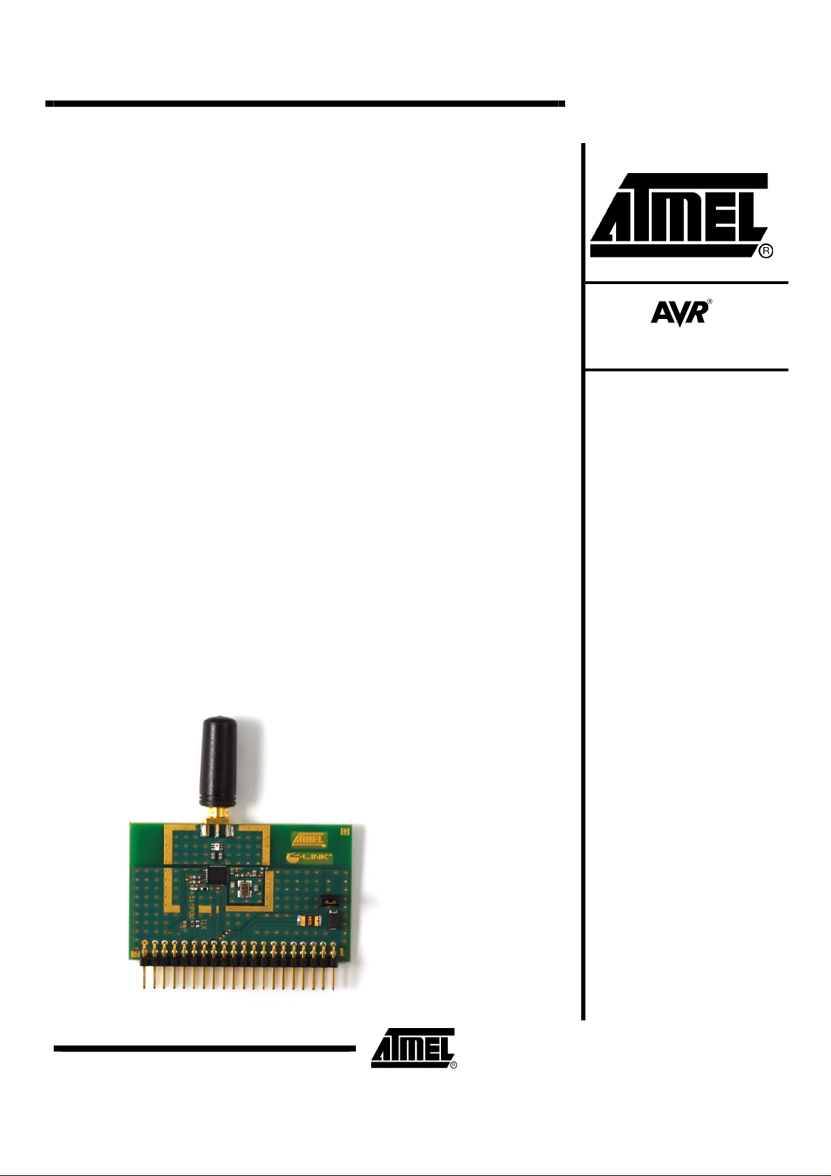
Figure 1-1. ATAVRRZ502 Accessory Kit
Rev. 8051A-AVR-11/06

2 Getting Started with the ATAVRRZ502 Accessory Kit
This section gives an introduction to what the ATAVRRZ502 Accessory Kit contains
and its system requirements. At the end brief instructions are given on how to get the
Accessory Kit up and running in the shortest amount of time.
2.1 Unpacking the System
Kit contents:
• (2 pcs) RZ502 Radio boards with SMA stub antennas.
• (2 pcs) ATmega1281V AVR
• Technical Library CD.
2.2 System Requirements
The minimum hardware and software requirements are:
• (2 pcs) STK®500
• (2 pcs) STK501
• (2 pcs) 9 pin RS-232 cable
• (2 pcs) 6-wire cable
• (2 pcs) 2-wire cable
• Power Supply for STK500.
• PC running AVR Studio
to-RS232 bridge).
®
microcontroller in TQFP Package.
®
and with two available RS-232 ports (COM port or USB-
2.3 Quick Start Guide
This section goes through how to get the RZ502 kit and evaluation application up and
running in the shortest amount of time.
1. Unpack the ATAVRRZ502 Accessory Kit and ensure that it contains all
components listed in subsection
2. Ensure that all the components listed in subsection
3. Go through the steps in section
to build both peers.
4. Generate EEPROM file for each peer in the network using the HEXMaker
application. How to use this application is described in subsection
5. Program the ATmega1281 microcontroller by following the instructions in
subsection
6. Finally, a chat client is available to interface with the evaluation application just
programmed into the AVR microcontroller. Go through the instructions in section
on how to setup and use the chat client.
5.2. Repeat this step on both peers.
2.1.
2.2 is available.
4 to assemble the hardware. Repeat this step twice
5.1.
6
2
AVR414
8051A-AVR-11/06
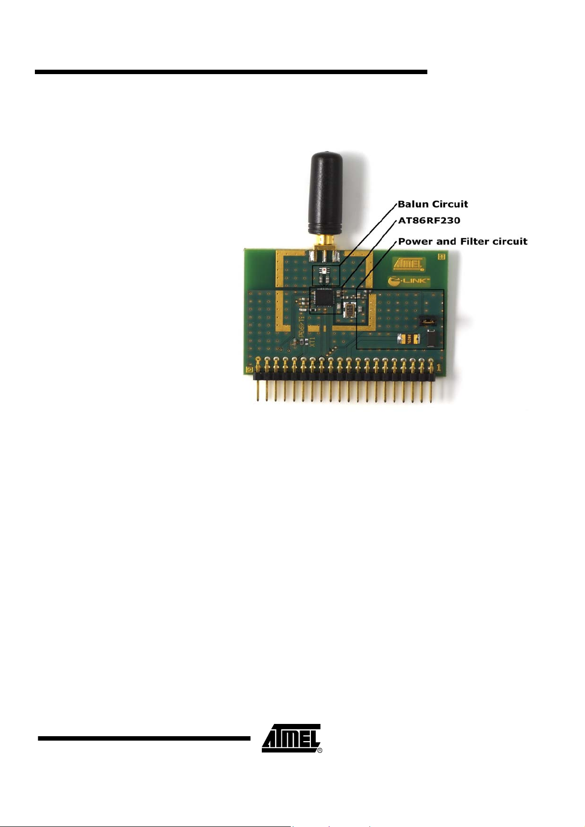
3 Hardware Description
Figure 3-1 ATAVRRZ502 Components
AVR414
3.1 Description of AT86RF230
The AT86RF230 is a 2.4 GHz radio transceiver from Atmel. It is specially designed for
IEEE 802.15.4 and ZigBee applications. Main features are:
• Low power consumption.
• Large link budget (104 dBm).
• True 1.8 volts operation.
• Minimized number of external components needed.
The only required external components are antenna, 16 MHz crystal and four
decoupling capacitors. An easy-to-use Serial Peripheral Interface (SPI) is defined for
accessing the radio’s register file. Please consult the AT86RF230 radio transceiver’s
datasheet for further information about its specifications, operating modes, registers
etc.
3.2 Description of Antenna and Balun Circuit
The antenna output of the AT86RF230 is differential. This configuration is beneficial
because:
• Immunity to electromagnetic interference.
• Immunity to power-supply noise.
• Immunity to ground noise.
• Suppression of even-order harmonic.
8051A-AVR-11/06
3
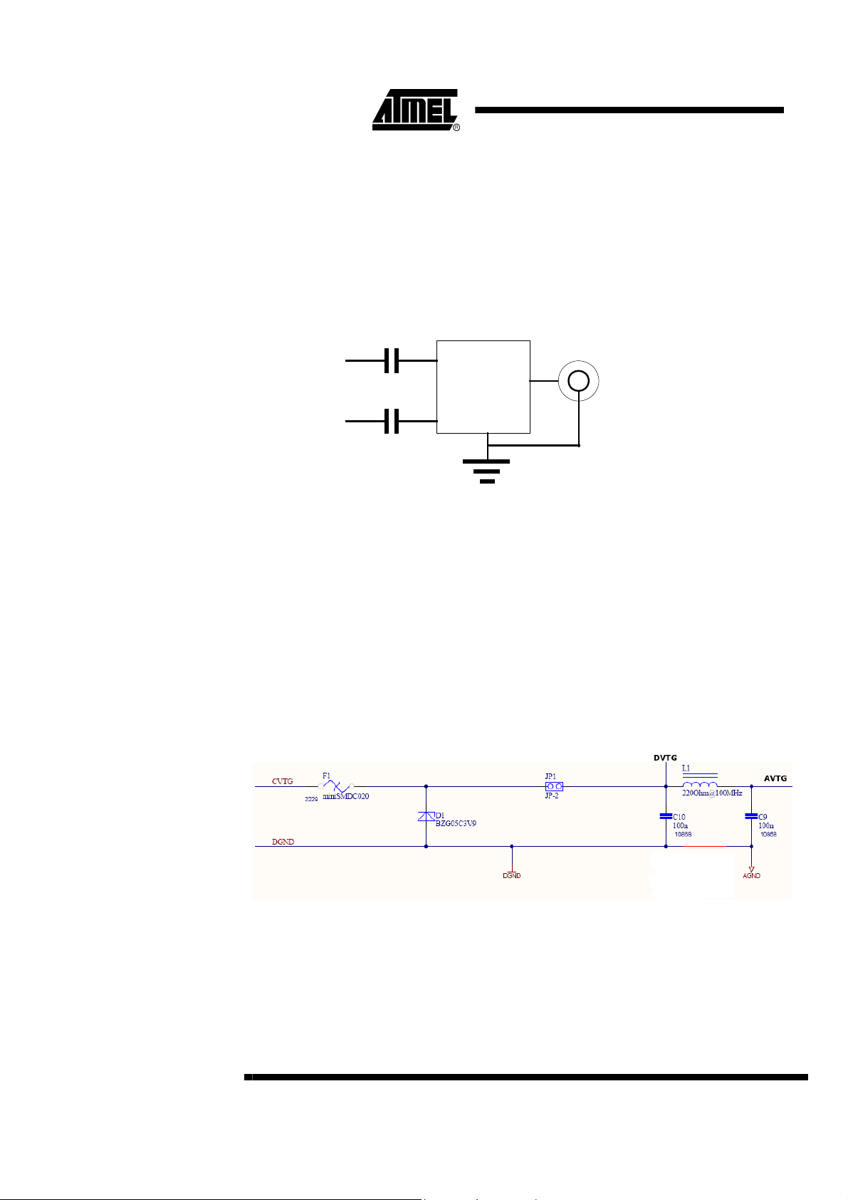
• Better tolerance to less than perfect RF ground.
However, the RZ502 has a typical single ended SMA stub antenna mounted. A
special circuit is required to convert the 100Ω differential RF input/output pins of the
AT86RF230 to a 50Ω single ended RF port. This is solved by a BALUN circuit on the
RZ502 top module. A BALUN (a compound term meaning “BAlanced-UNbalanced”) is
a passive component that transforms impedance. Two capacitors are added as a DC
Figure 3-2 depicts the BALUN circuit described above.
block.
Figure 3-2 BALUN Circuit
C1
RFN
BALUN
Balanced 1
Unbalanced
SMA Connector
RFP
3.3 Description of Power and Filter Circuit
Figure 3-3 shows the power and filter circuit connected to the AT86RF230. The power
circuit is built from three components; a SMD fuse (F1), a Zener diode (D1) and a
jumper (JP1). D1 is a 3.9 Volts Zener diode connected in series with the thermal fuse.
This connection prevents excessive voltages on the DVTG (Digital Voltage) and
AVTG (Analog Voltage) ports when JP1 is closed, and potentially harm the
AT86RF230. JP1 can also be used for current measurements.
The rightmost part of
inductor) filter used to suppress noise and harmonics to enter the analog/RF part of
the radio transceiver.
Figure 3-3 Power and Filter Circuit
Balanced 2
C2
Figure 3-3 is a PI-type LC (two shunt capacitors and one series
3.4 Description of STK500 Interface
The STK500 board has two expansion connectors, one on each side of the
programming module. All AVR I/O ports, programming signals and control signals are
routed to these connectors.
This connector is used by the RZ502 top module to mount itself to the
STK500/STK501 board stack. And ultimately connect the AT86RF230 radio
4
AVR414
Figure 3-4 depicts the pin-out of expansion connector 1.
8051A-AVR-11/06
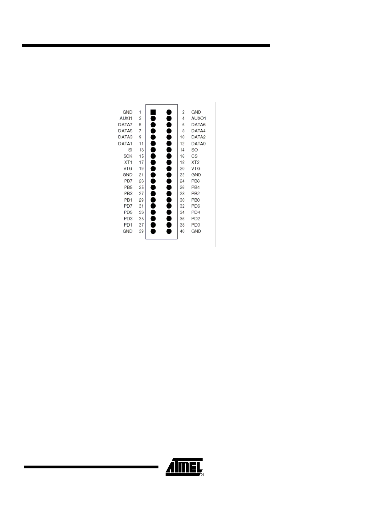
transceiver to the AVR microcontroller. Only a few of the available pins are used to
control the radio transceiver. The reminder of this subsection describes the interface
necessary to control the radio transceiver.
Figure 3-4 Expansion Connector 1 Pin-out
AVR414
3.4.1 SPI Lines
3.4.2 IRQ Line
3.4.3 SLP_TR Line
The SPI is used to program control registers as well as to transfer data frames
between the AVR and the AT86RF230. Each access is initiated with the SPI master
(AVR) pulling the slave select (SS/SEL) line low. Both master and slave (AT86RF230)
will now prepare the data to be sent, and the master generates the necessary clock
pulses on the SCLK line to interchange the data. Data is always transferred from
master to slave on the Master Out – Slave In, MOSI line, and from slave to master on
the Master In – Slave Out, MISO line. When a packet has been transmitted, the
master will pull high the slave select line to synchronize the slave.
The AT86RF230 has six different interrupts defined. However, all these interrupt
signals are combined internally via a logical “OR” operation to one external interrupt
line. An interrupt is indicated to the AVR microcontroller whenever the IRQ line is
pulled high (logical 1). The controller must poll the AT86RF230 to determine the
interrupt source and to clear the IRQ line.
The SLP_TR signal is a multi-functional pin. It can be used as either a transmit start
or a sleep signal. Pin functionality is dependant upon the transceiver’s internal state.
Please consult the datasheet of the AT86RF230 for more information.
8051A-AVR-11/06
5

3.4.4 Reset Line
3.4.5 Pins used by the RZ502
This line is used to reset the AT86RF230 radio transceiver. The reset line is
controlled by one of the AVR pins and not connected to the reset button on the
STK500 board.
Table 3-1 lists the 17 pins used by the RZ502 top module and their usage. This
information can be used to run the Accessory Kit on alternative platforms. Remaining
pins of the expansion connector 1 is not connected.
NOTE: Be sure that none of the pins used by the RZ502 top module is connected to
other circuitry. I.e. no additional circuitry can be connected to the SPI pins of the
PORTB connector on the STK500 etc.
Table 3-1
Expansion Connector 1 Pin Name Usage
Notes: 1. Pins connected to the same net. Only one required if number of pins is scarce.
. Pins used by the RZ502 board
1,2,21,22,39,40
19,20
17
25 PB5
26 PB4
27 PB3 MISO line.
28 PB2 MOSI line.
29 PB1 SCK line.
30 PB0 SEL line.
32 PD6
34 PD4
2. Not connected by default. Requires de-soldering R1 (0 Ω) and soldering onto
the R2 pads.
(1)
(1)
(2)
GND Used for analog and digital ground.
VTG
XT1
Target voltage. Must be within the
operating range of the AT86RF230 [1.8 to
3.6 Volts].
Can be used to connect the CLKM pin on
the AT86RF230 to the AVR’s XT1 pin.
Reset line. Connected to the RST pin on
the AT86RF230.
Connected to the SLP_TR pin on the
AT86RF230.
Used to connect the CLKM pin of the
AT86RF230 to the Timer1 module on the
AVR.
Connected to the IRQ pin on the
AT86RF230.
6
AVR414
8051A-AVR-11/06

4 Hardware Assembly
The following steps walk the reader through how to assemble and prepare the
STK500 board and the STK501 top module to be used with the RZ502. Then finally
how to mount the RZ502 board and configure it to run the evaluation application.
NOTE: The following steps must be completed successfully to ensure correct
operation of the hardware.
Step A. Assemble and configure the STK500 board
The jumpers and operating voltage of the STK500 board must be set up correct in
advance of mounting the STK501 and radio board.
1. Carefully remove any AVRs from the target sockets on the STK500.
2. Place jumpers on the following headers as shown in
• VTARGET
• AREF
• RESET
• BSEL2
3. Connect a serial cable to the connector marked RS232CTRL on the STK500 to a
COM port on the PC.
4. Apply power to the STK500 by moving the power switch toward the edge of the
board.
5. Start AVR Studio and press “Cancel” in the Welcome dialog window.
6. From the Tools menu, select “Program AVR” and “Connect…”.
7. Select “STK500 or AVRISP” as platform and then press “Connect…”. Verify that a
window named “STK500” appears.
8. Open the Board tab. Adjust the VTarget voltage and ARef voltage to 3 Volts. Press
the Write Voltages button. Close the STK500 window.
Figure 4-1:
AVR414
8051A-AVR-11/06
7

Figure 4-1 Jumper Placement on the STK500
Step B. Assemble and attach the STK501 Top Module
The jumpers are now set correctly and the target voltage is set to 3 volts. This
ensures that the AT86RF230 radio transceiver is not damaged and the ATmega1281
will run at 8MHz. The next steps describe how to mount the STK501 top module.
1. Insert an ATmega1281 into the Zero Insertion Force (ZIF) socket on the STK501.
Press the spring-loaded top frame of the ZIF down and gently aligning the device
underneath the fine-pitched wires. Verify that pin 1 on the TQFP package (dot in
one of its corners) points towards the notched corner of the ZIF.
2. Ensure that power is turned off on the STK500 board.
3. Connect the STK501 to the STK500 by using expansion header 0 and 1. Ensure
that the EXPAND0 written on the STK501 top module aligns with the EXPAND0
written beside the expansion header on the STK500 board.
4. Connect PINE1 and PINE2 to the RXD and TXD pins respectively. This can be
done using one of the 2-wire cables included in the STK500 starter kit. The RXD
and TXD pins are found close to the 9-pins RS-232 connector on the STK501.
5. To enable the In-System Programmer (ISP) interface, connect a 6-wire cable
between the ISP6PIN connector on the STK500 board and the SPROG connector
on the STK501 top module as shown in
Figure 4-2.
8
AVR414
8051A-AVR-11/06

Figure 4-2 Details of ISP Connection
AVR414
Step C. Mount the Radio Board
The RZ502 radio board is added to the STK501 by using its EXPAND1 header.
1. Find pin 1 on the radio board (Only square pad and with the digit 1 printed to its
right). This is pin must align with pin 1 on STK501’s EXPAND1 header.
2. Insert the radio board. Verify that the set up is equal to that shown in
Figure 4-3.
8051A-AVR-11/06
9

Figure 4-3 Complete Setup: STK500, STK501 and RZ502
5 How to Program the ATmega1281
With the hardware successfully assembled and configured for both peers it is time to
program them. This section describes how to do this using the STK500. Subsection
5.2 goes through the steps necessary to program the ATmega1281 with the
precompiled evaluation application. However in advance of doing this operation, an
EEPROM file must be generated that contains the 64-bit MAC address of each radio.
This operation is described in subsection
5.1 EEPROM File Generation
The IEEE 802.15.4 stack from Atmel uses the EEPROM of the AVR microcontroller to
store the unique 64-bit MAC address. An EEPROM file that contains this address
must be generated since the ATmega1281 is not preprogrammed with this
information.
NOTE: The MAC address printed on the RZ502 top module is for evaluation only. For
customer’s products a separate address must be obtained.
1. Locate the MAC address on the RZ502 board. The address is a 16-byte string
printed on a small white label (Ex. 00-04-25-FF-FF-17-03-E9).
2. Then start the HEXMaker command line tool found in the “bin” folder. This tool
takes two inputs; filename of the .hex file and the MAC address in 16-byte string
representation. Ex.:
>HEXMaker nodeA.hex 000425FFFF1703E9
Filename : nodeA.hex
MAC address : 00 04 25 FF FF 17 03 E9 (Byte order reversed in HEX file)
nodeA.hex created!
5.1.
10
AVR414
8051A-AVR-11/06

5.2 Programming the ATmega1281
The precompiled firmware used in the following subsection can be found in the “bin”
folder of the .zip file accompanying this document.
1. Connect a serial cable to the connector marked RS232CTRL on the STK500 to a
COM port on the PC.
2. Apply power to the STK500 by moving the power switch toward the edge of the
board.
3. Start AVR Studio and press the “Cancel” button in the Welcome dialog window.
4. From the Tools menu, select “Program AVR” and “Connect…”.
5. Select STK500 or AVRISP as platform and then press “Connect…”. Verify that a
dialog named “STK500 with STK501 top module” appears.
6. Open the “Program” tab. Select ATmega1281 from the Device pull down menu.
7. Select the “Fuses” tab and ensure that the Fuses are set as listed in
Table 5-1
Brown-out detection disabled Checked
Preserve EEPROM Checked
Boot Flash section size=4096 words Checked
Divide clock by 8 internally Not Checked
Int. RC Osc.;Start-up time: 6CK + 65 ms Checked
. ATmega1281 Fuse Settings
Fuse Name Setting Comment
This way the user only needs to
program the EEPROM once.
Will divide the clock by 8. This
will corrupt the MAC execution.
AVR414
Table 5-1:
8. Go back to the “Program” tab. Program the flash of the ATmega1281 with the
“bin\AVR414_evaluation_application.hex” file found in the “bin” folder.
9. Program the EEPROM of the ATmega1281 with the .hex file generated in
subsection
10. Close the STK500 window.
5.1.
6 Running the Evaluation Application
As mentioned in the introduction of this document an evaluation application is
available as a part of this application note. This is a peer-to-peer chat application,
where two RZ502 top modules are used to send messages back and forth.
gives an overview of the evaluation application and its components from a system
point of view. The reminder of this section describes two different ways to interface
with the evaluation application.
Figure 6-1
8051A-AVR-11/06
11

Figure 6-1 Overview of Evaluation Application
6.1 Terminal Mode
6.1.1 Command Interface
In terminal mode the user can talk directly to the evaluation application programmed
into the AVR microcontroller. This evaluation application is a thin layer of code that
defines a command interface on top of the IEEE 802.15.4 stack from Atmel. The
responsibilities of the evaluation application are:
• Start a new network.
• Associate to the network.
• Send data over the wireless link.
• Notify when new data is available.
• Reset the IEEE 802.15.4 MAC and evaluation application.
This section will describe the command interface that resides on top of the IEEE
802.15.4 MAC library. Commands are sent to the AVR microcontroller by using its
serial communication interface (USART). Every command described in the latter part
of this subsection can be tried out by connecting the STK501 top module to one of the
PC’s COM ports. Type in the test command in your favorite terminal application
(Hence the name terminal mode), append CR + LF (Carriage Return + Line Feed =
ASCII “\r\n”) before executing.
6.1.1.1 Reset (AT+R)
12
AVR414
Before continuing, the following formats are used in
• Characters in quotation marks are the actual text sent to the AVR.
• Optional commands and response parameters are enclosed in brackets.
The ”AT+R” command is used to reset the command interface and the IEEE 802.15.4
MAC. See
Table 6-1 for details.
Table 6-1 through Table 6-5:
8051A-AVR-11/06

6.1.1.2 Configure Network (AT+C)
AVR414
Table 6-1. AT command and possible responses
Command Response Comment
“AT+R” “OK” Reset successful.
”ERROR: 0x80” Syntax error.
”ERROR: 0x83” Reset unsuccessful.
The ”AT+C” command has two possible functions. It will either start a new network
and set up the peer to become a coordinator, or associate the device to an existing
network and set up the peer to be an end-device. See
Table 6-2 for details.
Table 6-2
Command Response Comment
“AT+C: [channel]1,[PANID]2,[role]3” “OK” Network configured.
”ERROR: 0x80” Syntax error.
”ERROR: 0x82” Wrong internal state.
”ERROR: 0x84” Unsupported role.
”ERROR: 0x85” Internal state is inconsistent
”ERROR: 0x86” Failed during active scan.
”ERROR: 0x87”
”ERROR: 0x88” Failed to start network.
”ERROR: 0x89” Failed to associate network.
”ERROR: 0x8B”
Notes: 1. Channel to start new network on or to associate. Valid channels are those
. AT command and possible responses
mlme_set_request primitive
failed.
One of the command’s
parameters is invalid.
defined by the IEEE 802.15.4 standard for the 2.4 GHz ISM band (channels 11
through 26). Must be in uppercase hexadecimal format. Ex.: 11 = 0B, 17 = 11.
2. PAN identifier of the network to start or associate. Valid range is that defined by
the IEEE 802.15.4 standard (0x0000 through 0xFFFF). Must be in uppercase
hexadecimal format. Ex.: 0 = 0000, 47789 = BAAD.
3. Role of the device. Only two valid alternatives. Either “C” for coordinator, or “E”
for end-device.
6.1.1.3 Send Data (AT+T)
8051A-AVR-11/06
The ”AT+T” command is used to send data over the wireless link established
between the two peers. See
Table 6-3
Command Response Comment
“AT+T: [length]1,[data]2” “OK” Data transmitted successful.
”ERROR: 0x80” Syntax error.
”ERROR: 0x81” Event buffer full.
”ERROR: 0x82” Wrong internal state.
”ERROR: 0x8A” Data transmission failed.
. AT command and possible responses
Table 6-3 for details.
13
6.1.1.4 Notifications (+N and +T)
Command Response Comment
”ERROR: 0x8B”
Notes: 4. Length in bytes of data payload.
5. Array containing the data payload.
One of the command’s
parameters is invalid.
The ”+N” and ”+T” commands are used to respectively indicate that a device has
associated to the network and that data was received. See
Table 6-4 and
Table 6-5 for details.
6.1.2 Examples using PC
Table 6-4
Command Response Comment
“+N”
. AT command and possible responses
Device associated successfully.
Only valid for coordinators.
Table 6-5. AT command and possible responses
Command Response Comment
“+T: [length]1,[data]2”
Notes: 1. Length in bytes of received data.
2. Array containing the received data.
Data received successfully.
Valid for both peers.
As mentioned previously all commands given in subsection 6.1.1.1 through
subsection 6.1.1.3 can be tested having the STK501 top module connected to a PC
using a RS232 cable. The default communication settings of the evaluation
application can be found in Table 6-6. The reminder of this subsection gives some
example scripts and comments.
Table 6-6
Setting Value Comment
Bits per second 38400
Data bits 8
Parity None
Stop bits 1
Flow control None CTS and DTS line not used.
. Communication Settings
6.1.2.1 Start a new network
14
AVR414
AT+R //Reset hardware and IEEE 802.15.4 Stack.
OK //Command terminated successfully.
AT+C: 0B,BAAD,C //Start network on channel 11 with PANID = BAAD.
8051A-AVR-11/06

6.1.2.2 Associate to network
6.1.2.3 Send data
OK //Network started.
AT+R //Reset hardware and IEEE 802.15.4 Stack.
OK //Command terminated successfully.
AT+C: 0B,BAAD,E //Associate to network on channel 11 with PANID =
//BAAD.
OK //Device associated. The coordinator will
//receive the “+N” notification.
AVR414
This script assumes that a peer-to-peer network with two devices has successfully
been established. An example on how to do this is outlined in subsection 6.1.2.1 and
subsection 6.1.2.2.
AT+T: 3,AVR //Send the string ”AVR” to the other peer.
OK //Data transmission finished. The receiving peer
//will be notified about the new data through the
//”+T” notification (“+T: 3,AVR”).
6.2 Graphical User Interface Mode
The Graphical User Interface (GUI) mode is the second method to interface with the
evaluation application (firmware running on the AVR). A small chat client (PC) written
in the Java
communication protocol used to control the evaluation application. The following
subsections guides the user through the steps required to successfully run the Java
based chat client.
NOTE: The chat client only supports the Microsoft
system. This is not due to the Java based implementation. But merely how the serial
port driver is implemented.
6.2.1 System Requirements
As mentioned in the introduction to subsection 6.2 the chat client is based on the
Java programming language. This is a programming language where the source code
is compiled into a byte code and then ran on a Java virtual machine (JVM). By default
this virtual machine does not support serial ports. The following steps show how to
install the Java virtual machine, add serial port support and ultimately how to connect
the STK500/RZ502 board stack to your PC.
®
programming language is available that hides some of the details of the
®
Windows® 2000 and XP operating
8051A-AVR-11/06
Step A: Install Java Runtime Environment.
15

The Java Runtime Environment (JRE) is a software bundle (JVM and libraries) that
allows your PC to run Java based applications. Following the steps is required to
ensure that the correct Java virtual machine is installed:
1. Go to Start Menu->Control Panel. Open the file named "Java". In the window that
opens, select the tab named "Java" and click on the "View..." button within the
"Java-Applet-Runtime-Settings" box.
2. A new dialog appears that lists the available JRE versions and their path.
3. Download and install the current JRE from Sun's Java Homepage
http://java.com/en/download/index.jsp) if no Java Runtime Environment was
(
found, or if the installed version is below version 1.5.x.
Step B: Install Serial Port Library.
The serial port library is installed by copying the files found in the "lib\pc" folder into
the following Java system folders:
1. Copy the "win32comm.dll" file to the "...\Java\jre1.5.x\bin" folder.
2. Copy the "comm.jar" file to the "...\Java\jre1.5.x\lib\ext" folder.
3. Copy the "javax.comm.properties" file to the "...\Java\jre1.5.x\lib" folder.
Step C: Connect STK501/RZ502 to your PC.
Connect a serial cable to the connector marked “RS232 SPARE #2” on the STK501
top module to a COM port on the PC as shown in Figure 6-2.
6.2.2 Running the Chat Client
Figure 6-2 STK501 with RS232 cable connected.
16
This subsection assumes that all the steps listed in subsection 5.1, 5.2 and 6.2.1
were completed successfully. The chat client is started by double clicking the file
AVR414
8051A-AVR-11/06

named “AVR414.jar” in the “bin” folder. A screen like that depicted in Figure 6-3
should now be visible. Now proceed with one of the following steps:
1. Step A: Start the Coordinator: Starts a new network. Peer becomes coordinator.
2. Step B: Start the End-device: Associate to an existing network. Peer becomes
end-device.
Figure 6-3 Chat Client Start Screen
AVR414
Step A: Start the Coordinator
3. From the screen shown in Figure 6-3, press the “Connect” button.
4. The “COM Settings” dialog box will now appear. From the drop down list, select the
serial port where the STK501 board is connected. Press “OK”.
5. Then in the “Device Options” dialog select the channel and PANID to start the
network on. Check the “Coordinator” option as seen in Figure 6-4. Press “OK”.
6. If the channel and PANID entered was valid, a new tab will be added to the chat
client containing a text area with the text: “Network not started yet”. This is just an
notification that an end-device must associate before it is possible to chat.
7. Proceed with Step B to add an end-device to the network.
8051A-AVR-11/06
17

Figure 6-4 Coordinator Options
Step B: Start the End-device
1. From the screen shown in Figure 6-3, press the “Connect” button.
2. The “COM Settings” dialog box will now appear. From the drop down list, select the
serial port where the STK501 board is connected. Press “OK”.
3. Then in the “Device Options” dialog select the same channel and PANID as for the
coordinator. Check the “End Device” option as seen in Figure 6-5. Press “OK”.
4. If it was possible to associate with the coordinator, a new tab will be added to the
chat client. It is now possible to send messages between the two peers.
5. Proceed with Step C for more information on how to chat.
Figure 6-5 End-device Options
18
Step C: Chatting
As seen in Figure 6-6 the chat window has two text areas and two buttons. The upper
text area is used to display the messages sent and received over the air. New
AVR414
8051A-AVR-11/06

messages are written in the lower text area, and sent by pressing the enter key or
“Send” button. “Clear” will erase the contents of the lower text area.
Going back to the initial tab (Debug) and pressing the “Disconnect” button terminates
the chat session.
Figure 6-6 Chat Window
AVR414
7 Troubleshooting Guide
Table 7-1. Troubleshooting Guide
Problem Reason Solution
Impossible to write to EEPROM Memory LockBits enabled
Ensure that the “Mode 1: No memory lock features
enabled” are selected in the LockBits tab of the
STK500 programmer’s window.
8 References
The following references were used when writing this application note:
• AT86RF230 Data Sheet, available from:
http://www.atmel.com/dyn/resources/prod_documents/doc5131.pdf
• IEEE 802.15.4 Standard.
• IEEE 802.15.4 MAC User Guide, available from:
http://www.atmel.com/dyn/resources/prod_documents/doc5182.pdf
9 Appendix – Additional Hardware Documentation
Intentionally left blank.
8051A-AVR-11/06
19

10 Table of Contents
Features...............................................................................................1
1 Introduction...................................................................................... 1
2 Getting Started with the ATAVRRZ502 Accessory Kit..................2
2.1 Unpacking the System ........................................................................................2
2.2 System Requirements.........................................................................................2
2.3 Quick Start Guide................................................................................................2
3 Hardware Description......................................................................3
3.1 Description of AT86RF230..................................................................................3
3.2 Description of Antenna and Balun Circuit ...........................................................3
3.3 Description of Power and Filter Circuit................................................................4
3.4 Description of STK500 Interface.........................................................................4
3.4.1 SPI Lines................................................................................................................... 5
3.4.2 IRQ Line.................................................................................................................... 5
3.4.3 SLP_TR Line............................................................................................................. 5
3.4.4 Reset Line................................................................................................................. 6
3.4.5 Pins used by the RZ502............................................................................................ 6
4 Hardware Assembly......................................................................... 7
5 How to Program the ATmega1281................................................10
5.1 EEPROM File Generation................................................................................. 10
5.2 Programming the ATmega1281........................................................................11
6 Running the Evaluation Application ............................................11
6.1 Terminal Mode...................................................................................................12
6.1.1 Command Interface................................................................................................. 12
6.1.2 Examples using PC................................................................................................. 14
6.2 Graphical User Interface Mode.........................................................................15
6.2.1 System Requirements............................................................................................. 15
6.2.2 Running the Chat Client .......................................................................................... 16
7 Troubleshooting Guide..................................................................19
8 References...................................................................................... 19
9 Appendix – Additional Hardware Documentation.......................19
10 Table of Contents......................................................................... 20
Disclaimer.............................................................................................21
20
AVR414
8051A-AVR-11/06

Disclaimer
Atmel Corporation
2325 Orchard Parkway
San Jose, CA 95131, USA
Tel: 1(408) 441-0311
Fax: 1(408) 487-2600
Regional Headquarters
Europe
Atmel Sarl
Route des Arsenaux 41
Case Postale 80
CH-1705 Fribourg
Switzerland
Tel: (41) 26-426-5555
Fax: (41) 26-426-5500
Asia
Room 1219
Chinachem Golden Plaza
77 Mody Road Tsimshatsui
East Kowloon
Hong Kong
Tel: (852) 2721-9778
Fax: (852) 2722-1369
Japan
9F, Tonetsu Shinkawa Bldg.
1-24-8 Shinkawa
Chuo-ku, Tokyo 104-0033
Japan
Tel: (81) 3-3523-3551
Fax: (81) 3-3523-7581
Disclaimer: The information in this document is provided in connection with Atmel products. No license, express or implied, by estoppel or otherwise, to any
intellectual property right is granted by this document or in connection with the sale of Atmel products. EXCEPT AS SET FORTH IN ATMEL’S TERMS AND
CONDITIONS OF SALE LOCATED ON ATMEL’S WEB SITE, ATMEL ASSUMES NO LIABILITY WHATSOEVER AND DISCLAIMS ANY EXPRESS, IMPLIED
OR STATUTORY WARRANTY RELATING TO ITS PRODUCTS INCLUDING, BUT NOT LIMITED TO, THE IMPLIED WARRANTY OF MERCHANTABILITY,
FITNESS FOR A PARTICULAR PURPOSE, OR NON-INFRINGEMENT. IN NO EVENT SHALL ATMEL BE LIABLE FOR ANY DIRECT, INDIRECT,
CONSEQUENTIAL, PUNITIVE, SPECIAL OR INCIDENTAL DAMAGES (INCLUDING, WITHOUT LIMITATION, DAMAGES FOR LOSS OF PROFITS, BUSINESS
INTERRUPTION, OR LOSS OF INFORMATION) ARISING OUT OF THE USE OR INABILITY TO USE THIS DOCUMENT, EVEN IF ATMEL HAS BEEN
ADVISED OF THE POSSIBILITY OF SUCH DAMAGES. Atmel makes no representations or warranties with respect to the accuracy or completeness of the
contents of this document and reserves the right to make changes to specifications and product descriptions at any time without notice. Atmel does not make any
commitment to update the information contained herein. Unless specifically provided otherwise, Atmel products are not suitable for, and shall not be used in,
automotive applications. Atmel’s products are not intended, authorized, or warranted for use as components in applications intended to support or sustain life.
© 2006 Atmel Corporation. All rights reserved. ATMEL®, logo and combinations thereof, Everywhere You Are®, AVR®, AVR Studio®, STK®
and others, are the registered trademarks or trademarks of Atmel Corporation or its subsidiaries. Windows
trademarks or trademarks of Microsoft
others.
®
Corporation in the US and/or other countries. Other terms and product names may be trademarks of
Atmel Operations
Memory
2325 Orchard Parkway
San Jose, CA 95131, USA
Tel: 1(408) 441-0311
Fax: 1(408) 436-4314
Microcontrollers
2325 Orchard Parkway
San Jose, CA 95131, USA
Tel: 1(408) 441-0311
Fax: 1(408) 436-4314
La Chantrerie
BP 70602
44306 Nantes Cedex 3, France
Tel: (33) 2-40-18-18-18
Fax: (33) 2-40-18-19-60
ASIC/ASSP/Smart Cards
Zone Industrielle
13106 Rousset Cedex, France
Tel: (33) 4-42-53-60-00
Fax: (33) 4-42-53-60-01
1150 East Cheyenne Mtn. Blvd.
Colorado Springs, CO 80906, USA
Tel: 1(719) 576-3300
Fax: 1(719) 540-1759
Scottish Enterprise Technology Park
Maxwell Building
East Kilbride G75 0QR, Scotland
Tel: (44) 1355-803-000
Fax: (44) 1355-242-743
RF/Automotive
Theresienstrasse 2
Postfach 3535
74025 Heilbronn, Germany
Tel: (49) 71-31-67-0
Fax: (49) 71-31-67-2340
1150 East Cheyenne Mtn. Blvd.
Colorado Springs, CO 80906, USA
Tel: 1(719) 576-3300
Fax: 1(719) 540-1759
Biometrics/Imaging/Hi-Rel MPU/
High Speed Converters/RF Datacom
Avenue de Rochepleine
BP 123
38521 Saint-Egreve Cedex, France
Tel: (33) 4-76-58-30-00
Fax: (33) 4-76-58-34-80
Literature Requests
www.atmel.com/literature
®
and others are registered
8051A-AVR-11/06
 Loading...