

Page 1

AT91SAM9XE-EK Evaluation Board
....................................................................................................................
User Guide
6311A–ATARM–04-Feb-08
Page 2

Table of Contents
Section 1
Overview .................................................................................................................... 1-1
1.1 Scope................................................................................................................................. 1-1
1.2 Deliverables ....................................................................................................................... 1-1
1.3 AT91SAM9XE-EK Evaluation Board ................................................................................. 1-1
Section 2
Setting Up the AT91SAM9XE-EK Board....................................................................2-1
2.1 Electrostatic Warning ......................................................................................................... 2-1
2.2 Requirements..................................................................................................................... 2-1
2.3 Layout ................................................................................................................................ 2-1
2.4 Powering Up the Board...................................................................................................... 2-4
2.5 Backup Power Supply........................................................................................................ 2-4
2.6 Getting Started................................................................................................................... 2-4
2.7 AT91SAM9XE-EK Block Diagram ..................................................................................... 2-5
Section 3
Board Description.......................................................................................................3-1
3.1 AT91SAM9XE 512/256/128 Microcontroller ...................................................................... 3-1
3.2 Block Diagram.................................................................................................................... 3-4
3.3 Microcontroller ................................................................................................................... 3-5
3.4 Memory.............................................................................................................................. 3-5
3.5 Clock Circuitry.................................................................................................................... 3-5
3.6 Reset Circuitry ................................................................................................................... 3-5
3.7 Shutdown Controller ..........................................................................................................3-5
3.8 Power Supply Circuitry.......................................................................................................3-5
3.9 Remote Communication .................................................................................................... 3-5
3.10 Audio Stereo Interface ....................................................................................................... 3-6
3.11 User Interface .................................................................................................................... 3-6
3.12 Debug Interface ................................................................................................................. 3-6
3.13 Expansion Slot................................................................................................................... 3-6
3.14 PIO Usage ......................................................................................................................... 3-7
Section 4
Configuration..............................................................................................................4-1
4.1 Jumpers ............................................................................................................................. 4-1
4.2 JTAG/ICE........................................................................................................................... 4-2
AT91SAM9XE-EK Evaluation Board User Guide i
6311A–ATARM–04-Feb-08
Page 3

Table of Contents (Continued)
4.3 Microcontroller Clock ......................................................................................................... 4-2
4.4 Memory Configuration........................................................................................................ 4-2
4.5 Ethernet ............................................................................................................................. 4-3
4.6 Miscellaneous .................................................................................................................... 4-3
Section 5
Schematics.................................................................................................................5-1
5.1 Schematics ........................................................................................................................ 5-1
Section 6
Revision History .........................................................................................................6-1
6.1 Revision History ................................................................................................................. 6-1
ii AT91SAM9XE-EK Evaluation Board User Guide
6311A–ATARM–04-Feb-08
Page 4

1.1 Scope
The AT91SAM9XE-EK evaluation kit enables the evaluation of and code development for applications
running on an AT91SAM9XE device.
This guide focuses on the AT91SAM9XE-EK board as an evaluation platform.
The board supports the AT91SAM9XE in an LFBGA217 package as well as in a PQFP208 package.
1.2 Deliverables
The AT91SAM9XE-EK package contains the following items:
an AT91SAM9XE-EK board
universal input AC/DC power supply with US, UK and Europe plug adapter
one A/B-type USB cable
one serial RS232 cable
one RJ45 crossed Ethernet cable
one CD-ROM that allows the user to begin evaluating the AT91 ARM® Thumb® 32-bit microcontroller
quickly.
Section 1
Overview
1.3 AT91SAM9XE-EK Evaluation Board
The board is equipped with an AT91SAM9XE (217-ball LFBGA package) together with the following:
64 Mbytes of SDRAM memory
256 Mbytes of NANDFlash memory
one Atmel serial DataFlash
one Atmel TWI serial EEPROM
one USB device port interface
two USB Host port interfaces
one DBGU serial communication port
one complete MODEM serial communication port
one additional serial communication port with RTS/CTS handshake control
JTAG/ICE debug interface
one PHY Ethernet 100-base TX with three status LEDs
one Atmel AT73C213 Audio DAC
one Power LED and one general-purpose LED
AT91SAM9XE-EK Evaluation Board User Guide 1-1
®
6311A–ATARM–04-Feb-08
Page 5

two user input push buttons
one Wakeup input push button
one reset push button
one DataFlash, SD/MMC card slot
four expansion connectors (PIOA, PIOB, PIOC, IMAGE SENSOR)
one BGA-like EBI expansion footprint connector
one Lithium Coin Cell Battery Retainer for 12 mm cell size
1-2 AT91SAM9XE-EK Evaluation Board User Guide
6311A–ATARM–04-Feb-08
Page 6

2.1 Electrostatic Warning
The AT91SAM9XE-EK evaluation board is shipped in protective anti-static packaging. The board must
not be subjected to high electrostatic potentials. A grounding strap or similar protective device should be
worn when handling the board. Avoid touching the component pins or any other metallic element.
2.2 Requirements
In order to set up the AT91SAM9XE-EK evaluation board, the following items are needed:
the AT91SAM9XE-EK evaluation board itself.
AC/DC power adapter (5V at 2A), 2.1 mm by 5.5 mm
2.3 Layout
Section 2
Setting Up the AT91SAM9XE-EK Board
AT91SAM9XE-EK Evaluation Board User Guide 2-1
6311A–ATARM–04-Feb-08
Page 7
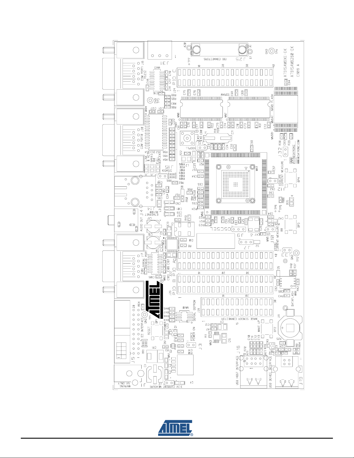
Figure 2-1. AT91SAM9XE-EK Layout-Top View
2-2 AT91SAM9XE-EK Evaluation Board User Guide
6311A–ATARM–04-Feb-08
Page 8
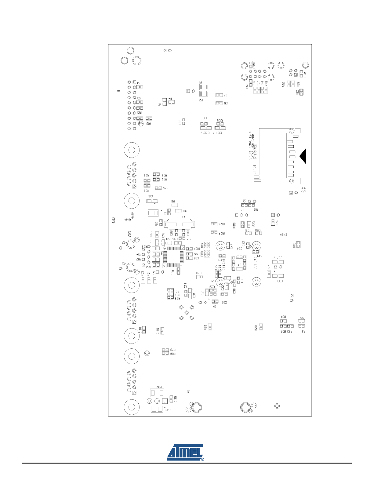
Figure 2-2. AT91SAM9XE-EK Layout - Bottom View
AT91SAM9XE-EK Evaluation Board User Guide 2-3
6311A–ATARM–04-Feb-08
Page 9

2.4 Powering Up the Board
The AT91SAM9XE-EK requires 5V DC (±5%). DC power is supplied to the board via the 2.1 mm by 5.5
mm socket J1. Coaxial plug center positive standard.
2.5 Backup Power Supply
The user has the possibility to plug a battery (3V Lithium Battery CR1225 or equivalent) in order to permanently power the backup part of the device. In this case, J10 configuration must be set in position 1, 2.
Refer to Section 4.1.
2.6 Getting Started
The AT91SAM9XE-EK evaluation board is delivered with a CD-ROM containing all necessary information and step-by-step procedures for working with the most common development toolchains. Please
refer to this CD-ROM, or to the AT91 web site, http://www.atmel.com/products/AT91/, for the most up-todate information on getting started with the AT91SAM9XE-EK.
2-4 AT91SAM9XE-EK Evaluation Board User Guide
6311A–ATARM–04-Feb-08
Page 10
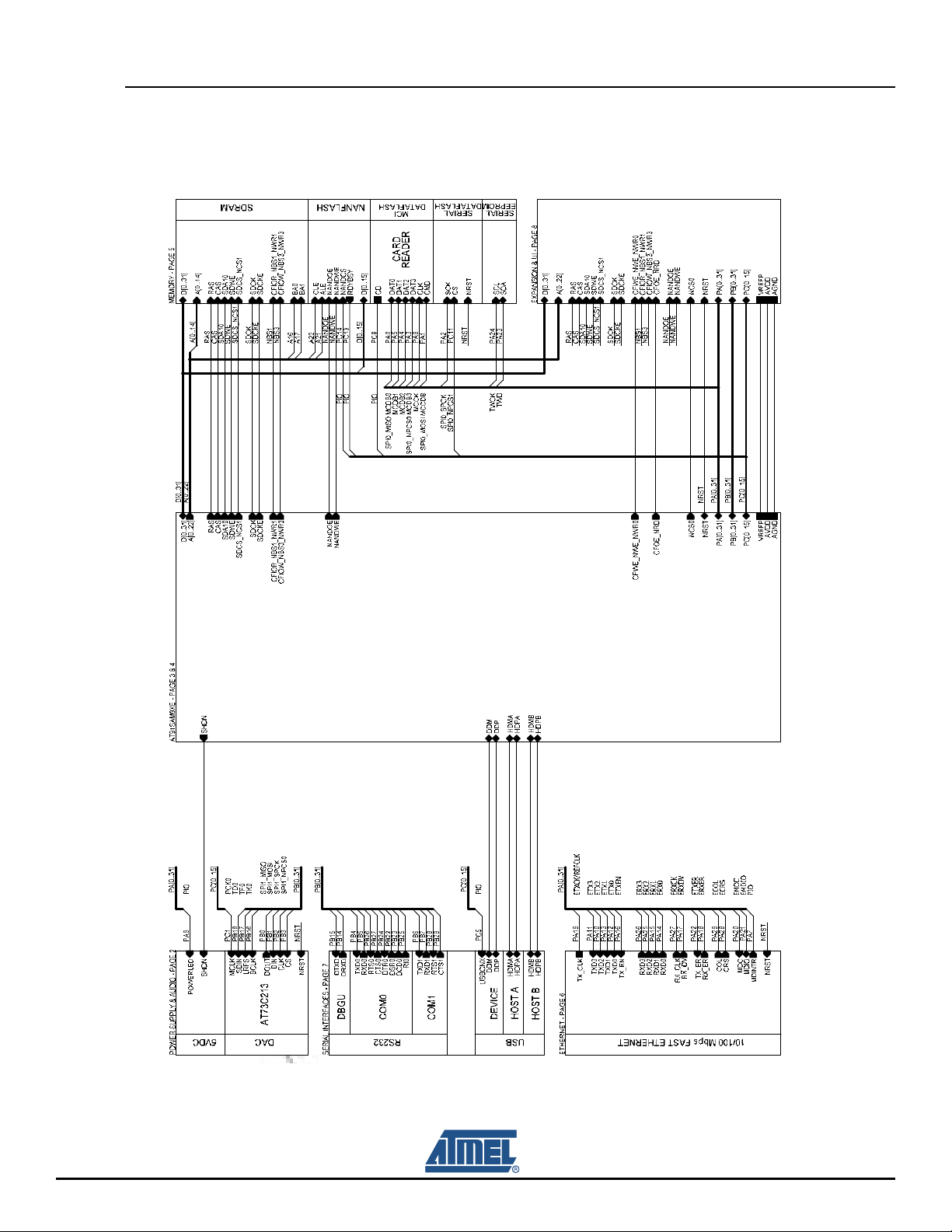
2.7 AT91SAM9XE-EK Block Diagram
Figure 2-3. AT91SAM9XE-EK Block Diagram
AT91SAM9XE-EK Evaluation Board User Guide 2-5
6311A–ATARM–04-Feb-08
Page 11

Section 3
Board Description
3.1 AT91SAM9XE 512/256/128 Microcontroller
• Incorporates the ARM926EJ-S
– DSP instruction Extensions, ARM Jazelle
– 8 Kbyte Data Cache, 16 Kbyte Instruction Cache, Write Buffer
– 200 MIPS at 180 MHz
– Memory Management Unit
– EmbeddedICE
™
, Debug Communication Channel Support
• Additional Embedded Memories
– One 32 Kbyte Internal ROM, Single-cycle Access at Maximum Matrix Speed
– One 32 Kbyte (for AT91SAM9XE256 and AT91SAM9XE512) or 16 Kbyte (for AT91SAM9XE128) Internal SRAM, Single-cycle
Access at Maximum Matrix Speed
– 128, 256 or 512 Kbytes of Internal High-speed Flash for AT91SAM9XE128, AT91SAM9XE256 or AT91SAM9XE512
Respectively. Organized in 256, 512 or 1024 Pages of 512 Bytes Respectively.
• 128-bit Wide Access
• Fast Read Time: 60 ns
• Page Programming Time: 4 ms, Including Page Auto-erase,
Full Erase Time: 10 ms
• 10,000 Write Cycles, 10 Years Data Retention, Page Lock Capabilities, Flash Security Bit
• Enhanced Embedded Flash Controller (EEFC)
– Interface of the Flash Block with the 32-bit Internal Bus
– Increases Performance in ARM and Thumb Mode with 128-bit Wide Memory Interface
• External Bus Interface (EBI)
– Supports SDRAM, Static Memory, ECC-enabled NAND Flash and CompactFlash
• USB 2.0 Full Speed (12 Mbits per second) Device Port
– On-chip Transceiver, 2,688-byte Configurable Integrated DPRAM
• USB 2.0 Full Speed (12 Mbits per second) Host Single Port in the 208-pin PQFP Device and Double Port in 217-ball LFBGA
Device
– Single or Dual On-chip Transceivers
– Integrated FIFOs and Dedicated DMA Channels
• Ethernet MAC 10/100 Base-T
– Media Independent Interface or Reduced Media Independent Interface
– 28-byte FIFOs and Dedicated DMA Channels for Receive and Transmit
• Image Sensor Interface
– ITU-R BT. 601/656 External Interface, Programmable Frame Capture Rate
– 12-bit Data Interface for Support of High Sensibility Sensors
– SAV and EAV Synchronization, Preview Path with Scaler, YCbCr Format
• Bus Matrix
– Six 32-bit-layer Matrix
– Remap Command
™
ARM® Thumb® Processor
®
Technology for Java® Acceleration
™
AT91SAM9XE-EK Evaluation Board User Guide 3-1
6311A–ATARM–04-Feb-08
Page 12

• Fully-featured System Controller, including
– Reset Controller, Shutdown Controller
– Four 32-bit Battery Backup Registers for a Total of 16 Bytes
– Clock Generator and Power Management Controller
– Advanced Interrupt Controller and Debug Unit
– Periodic Interval Timer, Watchdog Timer and Real-time Timer
• Reset Controller (RSTC)
– Based on a Power-on Reset Cell, Reset Source Identification and Reset Output Control
• Clock Generator (CKGR)
– Selectable 32,768 Hz Low-power Oscillator or Internal Low Power RC Oscillator on Battery Backup Power Supply,
Providing a Permanent Slow Clock
– 3 to 20 MHz On-chip Oscillator, One Up to 240 MHz PLL and One Up to 100 MHz PLL
• Power Management Controller (PMC)
– Very Slow Clock Operating Mode, Software Programmable Power Optimization Capabilities
– Two Programmable External Clock Signals
• Advanced Interrupt Controller (AIC)
– Individually Maskable, Eight-level Priority, Vectored Interrupt Sources
– Three External Interrupt Sources and One Fast Interrupt Source, Spurious Interrupt Protected
• Debug Unit (DBGU)
– 2-wire UART and support for Debug Communication Channel, Programmable ICE Access Prevention
• Periodic Interval Timer (PIT)
– 20-bit Interval Timer Plus 12-bit Interval Counter
• Watchdog Timer (WDT)
– Key-protected, Programmable Only Once, Windowed 16-bit Counter Running at Slow Clock
• Real-Time Timer (RTT)
– 32-bit Free-running Backup Counter Running at Slow Clock with 16-bit Prescaler
• One 4-channel 10-bit Analog to Digital Converter
• Three 32-bit Parallel Input/Output Controllers (PIOA, PIOB, PIOC,)
– 96 Programmable I/O Lines Multiplexed with up to Two Peripheral I/Os
– Input Change Interrupt Capability on Each I/O Line
– Individually Programmable Open-drain, Pull-up Resistor and Synchronous Output
• Peripheral DMA Controller Channels (PDC)
• Two-slot Multimedia Card Interface (MCI)
™
– SDCard/SDIO and MultiMediaCard
– Automatic Protocol Control and Fast Automatic Data Transfers with PDC
Compliant
• One Synchronous Serial Controllers (SSC)
– Independent Clock and Frame Sync Signals for Each Receiver and Transmitter
– I²S Analog Interface Support, Time Division Multiplex Support
– High-speed Continuous Data Stream Capabilities with 32-bit Data Transfer
• Four Universal Synchronous/Asynchronous Receiver Transmitters (USART)
®
– Individual Baud Rate Generator, IrDA
– Support for ISO7816 T0/T1 Smart Card, Hardware Handshaking, RS485 Support
– Full Modem Signal Control on USART0
Infrared Modulation/Demodulation
• One 2-wire UART
• Two Master/Slave Serial Peripheral Interface (SPI)
– 8- to 16-bit Programmable Data Length, Four External Peripheral Chip Selects
– Synchronous Communications
• Two Three-channel 16-bit Timer/Counters (TC)
– Three External Clock Inputs, Two Multi-purpose I/O Pins per Channel
– Double PWM Generation, Capture/Waveform Mode, Up/Down Capability
– High-Drive Capability on Outputs TIOA0, TIOA1, TIOA2
3-2 AT91SAM9XE-EK Evaluation Board User Guide
6311A–ATARM–04-Feb-08
Page 13

• Two Two-wire Interfaces (TWI)
– Master, Multi-master and Slave Mode Operation
– General Call Supported in Slave Mode
– Connection to PDC Channel to Optimize Data Transfers in Master Mode Only
®
• IEEE
1149.1 JTAG Boundary Scan on All Digital Pins
• Required Power Supplies:
– 1.65V to 1.95V for VDDBU, VDDCORE and VDDPLL
– 1.65V to 3.6V for VDDIOP1 (Peripheral I/Os)
– 3.0V to 3.6V for VDDIOP0 and VDDANA (Analog-to-digital Converter)
– Programmable 1.65V to 1.95V or 3.0V to 3.6V for VDDIOM (Memory I/Os)
• Available in a 208-pin PQFP Green and a 217-ball LFBGA Green Package
AT91SAM9XE-EK Evaluation Board User Guide 3-3
6311A–ATARM–04-Feb-08
Page 14

3.2 Block Diagram
Figure 3-1. AT91SAM9XE512/256/128 Block Diagram
HDMB
HDPB
HDMA
HDPA
ISI_HSYNC
ISI_DO-ISI_D7
ISI_PCK
F100
MDIO
MDC
ETX0-ETX3
ERX0-ERX3
ERXER-ERXDV
ECRS-ECOL
ETXEN-ETXER
ETXCK-ERXCK
JTAGSEL
RTCK
TCK
TMS
TDO
TDI
NTRST
ERASE
SLAVEMASTER
Transc.
USB
OHCI
Transc.
ISI_VSYNC
Image
Sensor
ISI_MCK
Interface
MAC
10/100 Ethernet
In-Circuit Emulator
JTAG Selection and Boundary Scan
System
ARM926EJ-S Processor
AIC
DBGU
Controller
DMA
DMA
FIFO
DMA
FIFO
6-layer Matrix
DCache
8 Kbytes
MMU
Bus Interface
ID
ICache
8 Kbytes
PDC
PMC
PLLA
PLLB
Filter
PITWDT
OSC
4GPREG
RC
RTT
OSC
A1/NBS2/NWR2
D0-D15
A0/NBS0
A2-A15, A18-A20
EBI
24-channel
Peripheral
16 or 32
Fast SRAM
ROM
32 Kbytes
Flash
or 512
128, 256
PIOA
PIOB
SHDC
A16/BA0
A17/BA1
NCS0
NCS1/SDCS
NAND Flash
CompactFlash
DMA
Peripheral
Bridge
Kbytes
Kbytes
PIOC
RSTC
POR
POR
NRD
NWR0/NWE
NWR1/NBS1
NWR3/NBS3
APB
BOD
A21/NANDALE
A22/NANDCLE
NANDOE, NANDWE
SDCK, SDCKE
RAS, CAS
SDWE, SDA10
Static
SDRAM
Controller
DPRAM
PDC
4-channel
PDC
SSC
TC3
TC0
PDC
PDC
USART0
PDC
PDC
NWAIT
D16-D31
Memory
Controller
USB
Device
10-bit ADC
TC4
TC5
TC1
TC2
SPI0
SPI1
USART1
USART2
TWI0
TWI1
MCI
A23-A24
NCS5/CFCS1
A25/CFRNW
NCS4/CFCS0
ECC
Controller
USART3
USART4
CFCE1-CFCE2
NCS2, NCS6, NCS7
NCS3/NANDCS
Transceiver
DDP
DDM
GNDANA
VDDANA
ADVREF
ADTRIG
AD0-AD3
RK
RF
RD
TD
TF
TK
MISO
MOSI
SPCK
NPCS0
NPCS1
NPCS2
NPCS3
DTR0
RI0
DCD0
DSR0
TWCK
TWD
MCCK
MCCDA
MCCDB
TIOB3-TIOB5
TIOA3-TIOA5
TCLK3-TCLK5
TIOB0-TIOB2
TIOA0-TIOA2
TCLK0-TCLK2
SPI0_, SPI1_
TXD0-TXD5
RXD0-RXD5
SCK0-SCK3
RTS0-RTS3
CTS0-CTS3
MCDA0-MCDA3
TST
FIQ
IRQ0-IRQ2
DTXD
DRXD
PLLRCA
PCK0-PCK1
XIN
XOUT
XIN32
XOUT32
OSCSEL
SHDN
WKUP
VDDBU
NRST
VDDCORE
MCDB0-MCDB3
3-4 AT91SAM9XE-EK Evaluation Board User Guide
6311A–ATARM–04-Feb-08
Page 15

3.3 Microcontroller
One LFBGA 217-ball device fitted on board
One LQFP 208-lead device footprint
To use the microcontroller in the LQFP package, the user has to unsolder MN4 and solder the PQFP208
microcontroller on the MN6 footprint.
3.4 Memory
32 Kbytes of Internal ROM
32 Kbyte of Internal SRAM
512 Kbytes of Internal High-speed Flash
Atmel serial DataFlash
64 Mbytes of SDRAM memory (32-bit bus width)
256 Mbytes of NANDFlash memory (8-bit bus width)
TWI serial EEPROM
3.5 Clock Circuitry
18.432 MHz standard crystal for the embedded oscillator
Selectable 32768Hz Low-power external standard crystal Oscillator or Internal Low Power RC
Oscillator
3.6 Reset Circuitry
Internal reset controller with bi-directional reset pin
External reset pushbutton
3.7 Shutdown Controller
Programmable shutdown and Wake-Up
Wake-up push button
3.8 Power Supply Circuitry
On-board 1.8V High Efficiency step-down charge pump regulator with shutdown control
On-board 3.3V linear regulator with shutdown control
3.9 Remote Communication
One serial interface (DBGU COM Port) via RS-232 DB9 male socket
One complete modem serial interface (COM Port 0) via RS-232 DB9 male socket
One additional serial interface (COM Port 1) with RTS/CTS handshake control via RS-232 DB9 male
AT91SAM9XE-EK Evaluation Board User Guide 3-5
6311A–ATARM–04-Feb-08
Page 16

socket
USB V2.0 full-speed compliant, 12 Mbits per second (UDP)
(1)
Tw o
One Ethernet 100-base TX with three status LEDs
USB Host ports V2.0 full-speed compliant, 12 Mbits per second (UHP)
3.10 Audio Stereo Interface
One Atmel stereo audio DAC (AT73C213)
One 32 Ohm/20 mW Stereo Headset output (J4) with master volume and mute controls
3.11 User Interface
Two user input pushbuttons
One user green LED
One yellow power LED (can be also software controlled)
3.12 Debug Interface
20-pin JTAG/ICE interface connector
DBGU COM port
(2)
3.13 Expansion Slot
One DataFlash, SD/MMC card slot
All I/Os of the AT91SAM9XE are routed to peripheral extension connectors
All I/Os of the AT91SAM9XE Image Sensor Interface are routed to peripheral extension connectors
All EBI Signals of the AT91SAM9XE are routed to extension footprint connectors (J25)
This allows the developer to check the integrity of the components and to extend the features of the
board by adding external hardware components or boards.
Notes: 1. Only one available with the 208-lead PQFP package.
2. Not available with the 208-lead PQFP package.
3-6 AT91SAM9XE-EK Evaluation Board User Guide
6311A–ATARM–04-Feb-08
Page 17

3.14 PIO Usage
Table 3-1. PIO Controller A
I/O Line Peripheral A Peripheral B Comments Function
PA0 SPI0_MISO MCDB0 SPI DATAFLASH, SPI/MCI SD/MMC/DATAFLASH Slot
PA1 SPI0_MOSI MCCDB (PA0..PA5)
PA 2 S P I0 _ S PC K
PA3 SPI0_NPCS0 MCDB3
PA 4 R TS 2 M CD B2
PA 5 C TS 2 M CD B1
PA6 MCDA0 User LED
PA7 MCCDA ETHERNET DM9161A MII/RMII (IRQ)
PA8 MCCK MCI SD/MMC/DATAFLASH Slot
PA9 MC DA 1 Po wer L ED
PA10 MCDA2 ETX2 ETHERNET DM9161A MII Interface (PA10..PA11)
PA 11 M C DA 3 E T X3
PA12 ETX0 ETHERNET DM9161A RMII Interface (PA12..PA19)
PA13 ETX1
PA14 ERX0
PA15 ERX1
PA16 ETXEN
PA17 ERXDV
PA 18 E R X ER
PA19 ETXCK
PA20 EMDC ETHERNET DM9161A MII/RMII Interface (PA20..PA21)
PA 21 E M DI O
PA22 ADTRG ETXER ETHERNET DM9161A MII Interface
PA23 TWD ETX2 SERIAL EEPROM (SDA)
PA24 TWCK ETX3 SERIAL EEPROM (SCL)
PA25 TCLK0 ERX2 ETHERNET DM9161A MII Interface (PA25..PA29)
PA26 TIOA0 ERX3 High-Drive
PA27 TIOA1 ERXCK High-Drive
PA28 TIOA2 ECRS High-Drive
PA29 SCK1 ECOL
PA30 SCK2 RXD4 (BP3) User's interface Push Button
PA31 SCK0 TXD4 (BP4) User's interface Push Button
AT91SAM9XE-EK Evaluation Board User Guide 3-7
6311A–ATARM–04-Feb-08
Page 18

Table 3-2. PIO Controller B
I/O Line Peripheral A Peripheral B Comments Function
PB0 SPI1_MISO TIOA3 Audio DAC AT73C213 (MISO)
PB1 SPI1_MOSI TIOB3 Audio DAC AT73C213 (MOSI)
PB2 SPI1_SPCK TIOA4 Audio DAC AT73C213 (SPCK)
PB3 SPI1_NPCS0 TIOA5 Audio DAC AT73C213 (Chip Select)
PB4 TXD0 COM PORT 0 (TXD)
PB5 RXD0 COM PORT 0 (RXD)
PB6 TXD1 TCLK1 COM PORT 1 (TXD)
PB7 RXD1 TCLK2 COM PORT 1 (RXD)
PB8 TXD2
PB9 RXD2
PB10 TXD3 ISI_D8 (J28) IMAGE SENSOR CONNECTOR (PB10..PB13)
PB11 RXD3 ISI_D9
PB12 TXD5 ISI_D10
PB13 RXD5 ISI_D11
PB14 DRXD SERIAL DEBUG PORT(RXD)
PB15 DTXD SERIAL DEBUG PORT(TXD)
PB16 TK0 TCLK3 Audio DAC AT73C213 (BCLK)
PB17 TF0 TCLk4 Audio DAC AT73C213 (LRFS)
PB18 TD0 TIOB4 Audio DAC AT73C213 (SDIN)
PB19 RD0 TIOB5 (J28) IMAGE SENSOR CONNECTOR (CTRL2)
PB20 RK0 ISI_D0 (J28) IMAGE SENSOR CONNECTOR (PB20..PB31)
PB21 RF0 ISI_D1
PB22 DSR0 ISI_D2 Warning: Shared with COM PORT 0 (PB22..PB27)
PB23 DCD0 ISI_D3
PB24 DTR0 ISI_D4
PB25 RI0 ISI_D5
PB26 RTS0 ISI_D6
PB27 CTS0 ISI_D7
PB28 RTS1 ISI_PCK Warning: Shared with COM PORT 1 (PB28..PB29)
PB29 CTS1 ISI_VSYNC
PB30 PCK0 ISI_HSYNC
PB31 PCK1 ISI_MCK
3-8 AT91SAM9XE-EK Evaluation Board User Guide
6311A–ATARM–04-Feb-08
Page 19

Table 3-3. PIO Controller C
I/O Line Peripheral A Peripheral B Comments Function
PC0 AD0 SCK3
PC1 AD1 PCK0 Audio DAC AT73C213 (MCLK)
PC2 AD2 PCK1
PC3 AD3 SPI1_NPCS3
PC4 A23 SPI1_NPCS2 (J28) IMAGE SENSOR CONNECTOR (CTRL1)
PC5 A24 SPI1_NPCS1 USB_CNX (VBUS DETECT)
PC6 TIOB2 CFCE1
PC7 TIOB1 CFCE2
PC8 NCS4/CFCS0 RTS3
PC9 NCS5/CFCS1 TIOB0
PC10 A25/CFRNW CTS3
PC11 NCS2 SPI0_NPCS1 SPI DATAFLASH memory (Chip Select)
PC12 IRQ0 NCS7
PC13 FIQ NCS6 NandFlash (RDYBSY)
PC14 NCS3/NANDCS IRQ2 NandFlash (NANDCS)
PC15 NWAIT IRQ1
PC16 D16 SPI0_NPCS2 EBI Data Bus (PC16..PC31)
PC17 D17 SPI0_NPCS3
PC18 D18 SPI1_NPCS1
PC19 D19 SPI1_NPCS2
PC20 D20 SPI1_NPCS3
PC21 D21 EF100
PC22 D22 TCLK5
PC23 D23
PC24 D24
PC25 D25
PC26 D26
PC27 D27
PC28 D28
PC29 D29
PC30 D30
PC31 D31
AT91SAM9XE-EK Evaluation Board User Guide 3-9
6311A–ATARM–04-Feb-08
Page 20

4.1 Jumpers
Table 4-1. Jumpers Configuration
Designation Default Setting Feature
J2 Closed 3.3V Jumper
Forces power on.
J3 Closed
J6 Closed VDDPLL Jumper
J7 2-3
J9 2 - 3
J10 Closed VDDBU Jumper
J12 Closed VDDCORE Jumper
To use the software shutdown control, J3 must be opened. 3V
battery backup must be present.
Erase/Normal operation mode
1-2: Erase entire flash chip
2-3 or open: Normal operating mode
Slow Clock OSCSEL
1-2: Internal RC Oscillator
2-3: External Crystal Oscillator
(1)
(1)
(1)
Section 4
Configuration
(1)
J15 Closed Enables Ethernet Auto MDIX control
J32 Closed Enables the use of the embedded NANDFLASH device (MN6xx)
J33 Closed Enables the use of the embedded DATAFLASH device (MN9)
Notes: 1. These jumpers are provided for power consumption measurement. By default, they are
closed. To use this feature, the user has to open the strap and insert an ammeter.
AT91SAM9XE-EK Evaluation Board User Guide 4-1
6311A–ATARM–04-Feb-08
Page 21

4.2 JTAG/ICE
Table 4-2. JTAG/ICE Configuration
Designation Default Setting Feature
S1 Opened Disables the ICE NTRST input
S2 Opened Selects ICE mode or JTAG mode
S3 Opened
R13 Soldered Enables the ICE RTCK return. S3 must be opened
R14 Soldered Enables the ICE NRST input
4.3 Microcontroller Clock
Table 4-3. Microcontroller Clock Configuration
Designation Default Setting Feature
R18/R20 Soldered
S4 Opened
J9 Slow Clock Setting. See
4.4 Memory Configuration
Table 4-4. Memory Configuration
Disables TCK <-> RTCK local loop. If S3 is closed, R13 must be
unsoldered.
Enables the use of 18.432MHz crystal. If an external clock is used,
R18/R20 must be unsoldered and S4 closed.
Table 4-1.
Designation Default Setting Feature
SDRAM
R31
R32
NAND Flash (MN6x)
R34
S6
SERIAL DATAFLASH (MN9)
S5 Opened Disables the write protection.
TWI SERIAL EEPROM (MN10)
R46
R47
4-2 AT91SAM9XE-EK Evaluation Board User Guide
6311A–ATARM–04-Feb-08
Soldered
Soldered
Soldered
Opened
Soldered
Soldered
Enables MN7 Chip select access
Enables MN8 Chip select access
Enables the use of Ready Busy signal
Disables write protection.
Enables SCL access
Enables SDA access
Page 22

4.5 Ethernet
RMII is the factory default mode.
To evaluate the MII mode, the user has to unsolder R49, R50, R127, close S7, S8 and populate R119 to
R126, C88, C89, Y4.
4.6 Miscellaneous
Refer to the TOP level schematic for the PIO usage.
Table 4-5. Miscellaneous
Designation Default Setting Feature
R82 Soldered USB DEVICE: Enables the use of the USBCNX signal
R72
R73
R94
R95
R96
R98
R101
R103
R104
R105
R106
R83
R85
R86
R88
TP1 N.A GND Test point
Soldered
Soldered
Soldered
Soldered
Soldered
Soldered
DBGU COM Port: Enables the use of DTXD output signal.
Enables the use of DRXD input.
RS232 COM Port 0: Enable the use of output signals.
RTS0
TXD0
DTR0
RS232 COM Port 0: Enable the use of input signals.
DCD0
DSR0
RXD0
CTS0
RI0
Enables all MAX3241E outputs buffer
RS232 COM Port 1: Enables the use of output signals.
TXD1
RTS1
RS232 COM Port 1: Enables the use of input signals.
RXD1
CTS1
TP2 N.A GND Test point.
TP3 N.A GND Test point.
TP4 N.A GND Test point.
TP5 N.A Reserved: do not use
TP6 N.A Reserved: do not use
AT91SAM9XE-EK Evaluation Board User Guide 4-3
6311A–ATARM–04-Feb-08
Page 23

5.1 Schematics
This section contains the following schematics:
Board Diagram - Schematic Top Level
Power supply and audio
217-ball BGA AT91SAM9XE Microcontroller
208-pin LQFP AT91SAM9XE Microcontroller
Memory
Ethernet
Serial Interface
Expansion and User Interface
Section 5
Schematics
AT91SAM9XE-EK Evaluation Board User Guide 5-1
6311A–ATARM–04-Feb-08
Page 24

Page 25

Page 26

Page 27

Page 28

Page 29

Page 30

Page 31

Page 32

6.1 Revision History
Table 6-1.
Document Comments
6311A First issue.
Section 6
Revision History
Change Request
Ref.
AT91SAM9XE-EK Evaluation Board User Guide 6-1
6311A–ATARM–04-Feb-08
Page 33

6-2 AT91SAM9XE-EK Evaluation Board User Guide
6311A–ATARM–04-Feb-08
Page 34

Headquarters International
Atmel Corporation
2325 Orchard Parkway
San Jose, CA 95131
USA
Tel: 1(408) 441-0311
Fax: 1(408) 487-2600
Atmel Asia
Room 1219
Chinachem Golden Plaza
77 Mody Road Tsimshatsui
East Kowloon
Hong Kong
Tel: (852) 2721-9778
Fax: (852) 2722-1369
Product Contact
Web Site
www.atmel.com
www.atmel.com/AT91SAM
Literature Requests
www.atmel.com/literature
Atmel Europe
Le Krebs
8, Rue Jean-Pierre Timbaud
BP 309
78054 Saint-Quentin-enYvelines Cedex
France
Tel: (33) 1-30-60-70-00
Fax: (33) 1-30-60-71-11
Technical Support
AT91SAM SupportAtmel techincal
support
Atmel Japan
9F, Tonetsu Shinkawa Bldg.
1-24-8 Shinkawa
Chuo-ku, Tokyo 104-0033
Japan
Tel: (81) 3-3523-3551
Fax: (81) 3-3523-7581
Sales Contacts
www.atmel.com/contacts/
Disclaimer: The information in this document is provided in connection with Atmel products. No license, express or implied, by estoppel or otherwise, to any
intellectual property right is granted by this document or in connection with the sale of Atmel products. EXCEPT AS SET FORTH IN ATMEL’S TERMS AND CONDI-
TIONS OF SALE LOCATED ON ATMEL’S WEB SITE, ATMEL ASSUMES NO LIABILITY WHATSOEVER AND DISCLAIMS ANY EXPRESS, IMPLIED OR STATUTORY
WARRANTY RELATING TO ITS PRODUCTS INCLUDING, BUT NOT LIMITED TO, THE IMPLIED WARRANTY OF MERCHANTABILITY, FITNESS FOR A PARTICULAR
PURPOSE, OR NON-INFRINGEMENT. IN NO EVENT SHALL ATMEL BE LIABLE FOR ANY DIRECT, INDIRECT, CONSEQUENTIAL, PUNITIVE, SPECIAL OR INCIDENTAL DAMAGES (INCLUDING, WITHOUT LIMITATION, DAMAGES FOR LOSS OF PROFITS, BUSINESS INTERRUPTION, OR LOSS OF INFORMATION) ARISING OUT OF
THE USE OR INABILITY TO USE THIS DOCUMENT, EVEN IF ATMEL HAS BEEN ADVISED OF THE POSSIBILITY OF SUCH DAMAGES. Atmel makes no
representations or warranties with respect to the accuracy or completeness of the contents of this document and reserves the right to make changes to specifications
and product descriptions at any time without notice. Atmel does not make any commitment to update the information contained herein. Unless specifically provided
otherwise, Atmel products are not suitable for, and shall not be used in, automotive applications. Atmel’s products are not intended, authorized, or warranted for use
as components in applications intended to support or sustain life.
© 2007 Atmel Corporation. All rights reserved. Atmel®, logo and combinations thereof, DataFlash® and others are registered trademarks or
trademarks of Atmel Corporation or its subsidiaries.ARM
®
, the ARMPowered® logo and others are registered trademarks or trademarks of ARM
Ltd. Other terms and product names may be trademarks of others.
6311A–ATARM–04-Feb-08
 Loading...