


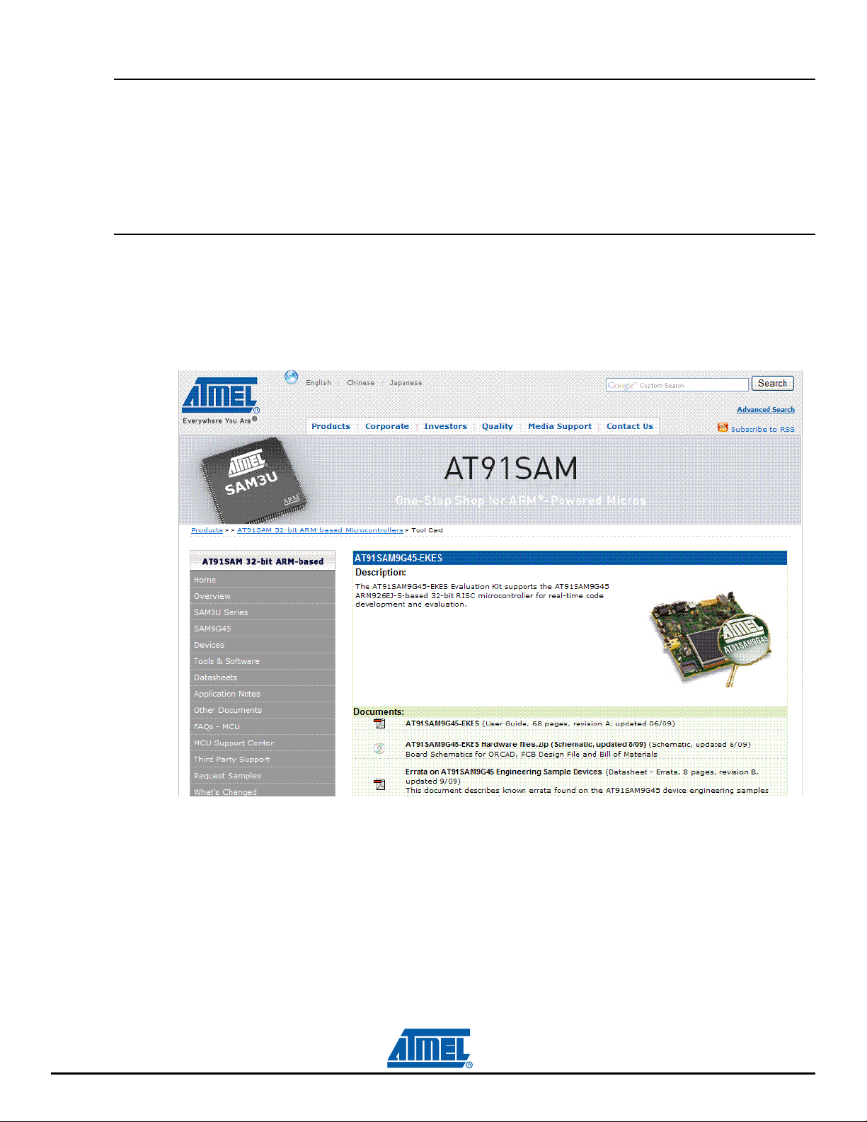
AT91SAM9G45-EKES
....................................................................................................................
User Guide
6481B–ATARM–27-Nov-09

Section 1
Introduction.................................................................................................................1-1
1.1 Scope ................................................................................................................................. 1-1
1.2 Applicable Documents ....................................................................................................... 1-2
Section 2
Kit Contents ................................................................................................................2-1
2.1 Deliverables ....................................................................................................................... 2-1
2.2 Evaluation Board Specifications......................................................................................... 2-2
2.3 Electrostatic Warning ......................................................................................................... 2-2
Section 3
Power Up....................................................................................................................3-1
3.1 Power Up the Board...........................................................................................................3-1
3.2 Battery................................................................................................................................ 3-1
3.3 DevStart ............................................................................................................................. 3-1
3.4 Recovery Procedure .......................................................................................................... 3-1
3.5 Sample Code and Technical Support ................................................................................ 3-2
Section 4
Board Description .......................................................................................................4-1
4.1 Equipment on the Board .................................................................................................... 4-1
4.1.1 Interfaces ............................................................................................................. 4-1
4.1.2 Board Interface Connection ................................................................................. 4-2
4.1.3 Push Button Switches .......................................................................................... 4-2
4.1.4 Display LCD and LEDs ........................................................................................ 4-3
4.2 Hardware Layout and Configuration .................................................................................. 4-3
4.2.1 Processor............................................................................................................. 4-3
4.2.2 Clock Circuitry...................................................................................................... 4-3
4.2.3 Reset Circuitry ..................................................................................................... 4-4
4.2.4 Memory................................................................................................................ 4-4
4.2.5 Power Supplies .................................................................................................... 4-7
4.2.6 Debug Interface ................................................................................................... 4-9
4.2.7 Audio Stereo Interface ....................................................................................... 4-14
4.2.8 TV-Out Extension .............................................................................................. 4-16
4.2.9 Software Controlled LEDs ................................................................................. 4-16
4.2.10 Serial Peripheral Interface Controller (SPI) ....................................................... 4-17
4.2.11 Two Wire Interface (TWI)................................................................................... 4-18
4.2.12 SD/MMC Interface ............................................................................................. 4-18
4.2.13 TFT LCD with Touch Panel ............................................................................... 4-20
4.2.14 Push Buttons ..................................................................................................... 4-22
AT91SAM9G45-EKES User Guide 1-i
6481B–ATARM–27-Nov-09

4.2.15 Expansion Slot ................................................................................................... 4-22
Section 5
Configuration ..............................................................................................................5-1
5.1 JTAG/ICE Configuration..................................................................................................... 5-1
5.2 ETHERNET Configuration ................................................................................................. 5-1
5.3 Jumpers Configuration ....................................................................................................... 5-2
5.4 Miscellaneous Configuration Items .................................................................................... 5-3
5.5 PIO Configuration............................................................................................................... 5-3
5.5.1 Peripheral Signals Multiplexing on I/O Lines ....................................................... 5-3
5.5.2 Multiplexing on PIO Controller A (PIOA).............................................................. 5-4
5.5.3 Multiplexing on PIO Controller B (PIOB).............................................................. 5-5
5.5.4 Multiplexing on PIO Controller C (PIOC) ............................................................. 5-6
5.5.5 Multiplexing on PIO Controller D (PIOD) ............................................................. 5-7
5.5.6 Multiplexing on PIO Controller E (PIOE).............................................................. 5-8
Section 6
Connectors .................................................................................................................6-1
6.1 Power Supply ..................................................................................................................... 6-1
6.2 RS232 Connector with RTS/CTS Handshake Support ...................................................... 6-1
6.3 DBGU................................................................................................................................. 6-2
6.4 Ethernet.............................................................................................................................. 6-3
6.5 USB Host ........................................................................................................................... 6-3
6.6 USB Host/Device ............................................................................................................... 6-4
6.7 JTAG Debugging Connector .............................................................................................. 6-4
6.8 SD/MMC- MCI0.................................................................................................................. 6-6
6.9 SD/MMC- MCI1.................................................................................................................. 6-7
6.10 AC97 .................................................................................................................................. 6-7
6.11 Image Sensor - ISI ............................................................................................................. 6-8
6.12 Video .................................................................................................................................. 6-9
6.13 Display Devices.................................................................................................................. 6-9
6.13.1 LG TFT LCD LG/PHILIPS.................................................................................... 6-9
6.14 Large LCD Extension ....................................................................................................... 6-10
Section 7
Schematics .................................................................................................................7-1
7.1 Schematics......................................................................................................................... 7-1
Section 8
Revision History..........................................................................................................8-1
8.1 Revision History ................................................................................................................. 8-1
1-ii AT91SAM9G45-EKES User Guide
6481B–ATARM–27-Nov-09
1.1 Scope
Section 1
Introduction
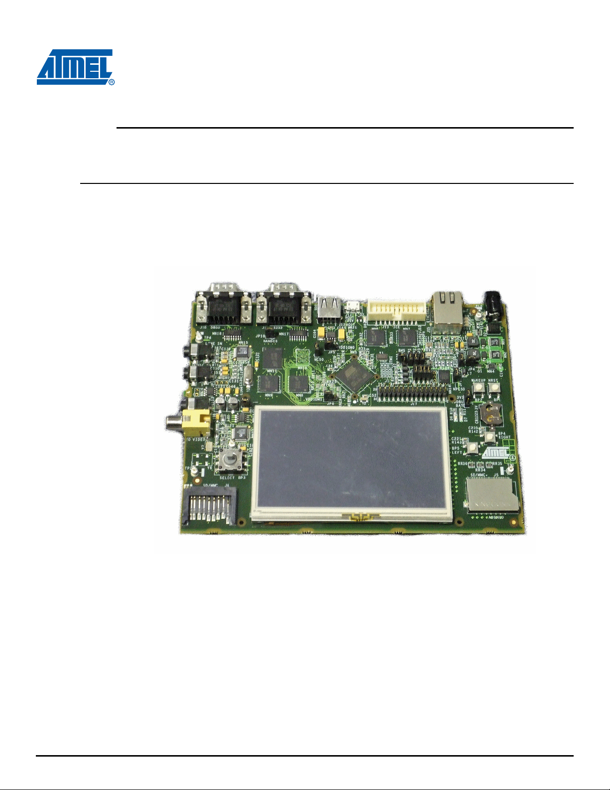
This User Guide introduces the SAM9G45 Evaluation Kit (SAM9G45-EKES) and describes its development and debugging capabilities.
Figure 1-1. Board Photo
The Atmel® SAM9G45-EKES is a fully-featured evaluation platform for the Atmel SAM9G45-based
microcontroller. The evaluation kit allows users to extensively evaluate, prototype and create applicationspecific designs.
The SAM9G45-EKES includes many hardware peripherals such as:
Two high speed USB hosts and one high speed device port
An Ethernet 10/100 interface
Two high speed multimedia card interfaces
An LCD TFT display (480*RGB*272)
A composite video output
AT91SAM9G45-EKES User Guide 1-1
6481B–ATARM–27-Nov-09
Introduction
A camera interface
Several communication peripherals such as:
– Universal Synchronous/Asynchronous Receiver Transmitter (USART)
– Serial Synchronous Controller (SSC)
– Two-Wire Interface (TWI)
The external memory block is made of 3 memory types:
DDR2-SDRAM
NAND Flash
NOR Flash
1.2 Applicable Documents
Table 1-1. Applicable Documents
Reference Title Comments
6438A SAM9G45 Preliminary Datasheet
6485A
Errata on AT91SAM9G45
Engineering Sample Devices
This document describes the SAM9G45, which is
part of the Atmel's Smart ARM
®
Microcontrollers.
It is available from
http://www.atmel.com/dyn/products/product_card.
asp?part_id=4596
It is available from
http://www.atmel.com/dyn/products/product_card.
asp?part_id=4596
1-2 AT91SAM9G45-EKES User Guide
6481B–ATARM–27-Nov-09
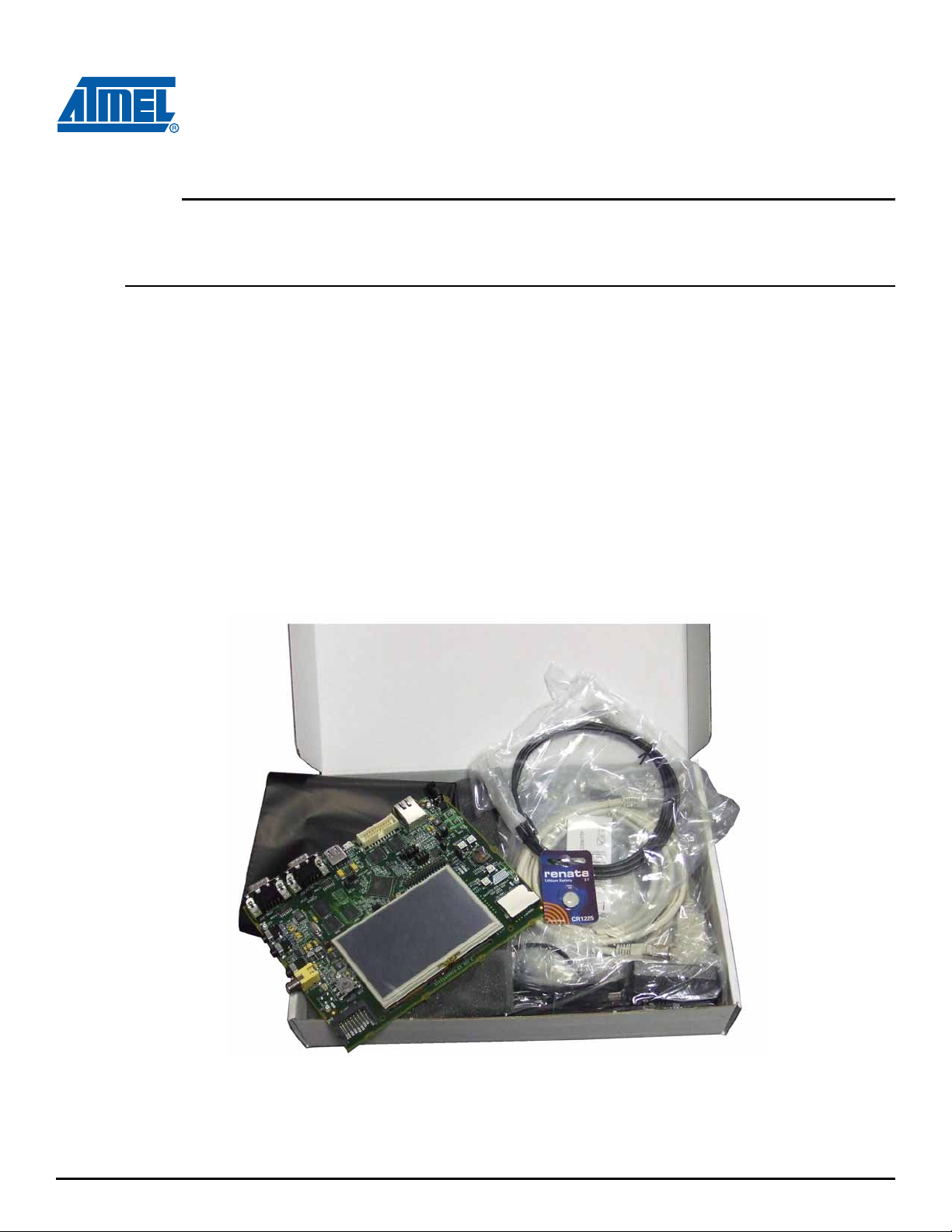
2.1 Deliverables
The Atmel SAM9G45-EKES toolkit includes:
Board
– The SAM9G45-EKES board
Power supply
– Universal input AC/DC power supply with US, Europe and UK plug adapters
– One 3V Lithium Battery type CR1225
Cables
– One micro A/B-type USB cable
– One serial RS232 cable
A Welcome Letter
Figure 2-1. Unpacked SAM9G45-EKES
Section 2
Kit Contents
Unpack and inspect this kit carefully. Contact your local Atmel distributor, should you have issues concerning the contents of the kit.
AT91SAM9G45-EKES User Guide 2-1
6481B–ATARM–27-Nov-09
Kit Contents
2.2 Evaluation Board Specifications
Table 2-1. SAM9G45-EKES Specifications
Characteristics Specifications
Clock speed 400 MHz PCK, 133 MHz MCK
Ports Ethernet, USB, RS232, DBGU
Board supply voltage 5 VDC from connector
Temperature
- operating
- storage
Relative humidity 0 to 90% (non condensing)
Dimensions 180 mm x 160 mm
RoHS status Compliant
-10° to +50° C
-40° to +85° C
2.3 Electrostatic Warning
The SAM9G45-EKES evaluation board is shipped in a protective anti-static package. The board must
not be subjected to high electrostatic potentials. We strongly recommend using a grounding strap or sim
ilar ESD protective device when handling the board in hostile ESD environments (offices with synthetic
carpet, for example...). Avoid touching the component pins or any other metallic element on the board.
-
2-2 AT91SAM9G45-EKES User Guide
6481B–ATARM–27-Nov-09

3.1 Power Up the Board
Unpack the board taking care to avoid electrostatic discharge. Unpack the power supply, select the right
power plug adapter corresponding to that of your country, and insert it in the power supply.
Connect the power supply DC connector to the board and plug the power supply to an AC power plug.
The board LCD should light up and display a welcome page. Then, click or touch icons displayed on the
screen and enjoy the demo.
3.2 Battery
The SAM9G45-EKES ships with a 3V coin battery.
This battery is not required for the board to start up.
The coin battery is provided for user convenience in case the user would like to exercise the date and
time backup function of the SAM9G45 series devices when the board is switched off.
Section 3
Power up
3.3 DevStart
The on-board NAND Flash contains a “SAM9G45-EKES DevStart”.
It is stored in the “SAM9G45-EKES DevStart” folder on the USB Flash disk available when the
SAM9G45-EKES is connected to a host computer.
Click the file “welcome.html” in this folder to launch SAM9G45-EKES DevStart.
SAM9G45-EKES DevStart guides you through installation processes of IAR™ EWARM, Keil MDK and
GNU toolkits. Then, it gives you step-by-step instructions on how to rebuild a single example project and
how to program it into the SAM9G45-EKES. Optionally, if you have a SAM-ICE™, instructions are also
given about how to debug the code.
We recommend that you backup the “SAM9G45-EKES DevStart” folder on your computer before
launching it.
AT91SAM9G45-EKES User Guide 3-1
6481B–ATARM–27-Nov-09
Power up
3.4 Recovery Procedure
The DevStart ends by giving step-by-step instructions on how to recover the SAM9G45-EKES to the
state as it was when shipped by Atmel.
Follow the instructions if you deleted the contents of the embedded Flash or the NAND Flash and want
to recover from this situation.
3.5 Sample Code and Technical Support
After boot up, you can run some sample code or your own application on the development kit. You can
download sample code and get technical support from Atmel website
http://www.atmel.com/dyn/products/tools_card.asp?tool_id=4597
Figure 3-1. Atmel Website for SAM9G45 Series
3-2 AT91SAM9G45-EKES User Guide
6481B–ATARM–27-Nov-09

4.1 Equipment on the Board
PARALLEL
FLASH
AT91SAM9M10
AT91SAM9G45
DEBUG
DEBUG
JTAG/ICEDBGU
System Controller
System Controller
External Memory
External Memory
EBI0
EBI0
EBI1 / 1.8v
EBI1 / 1.8v
DDR2
SDRAM
DDR2
SDRAM
NAND
FLASH
Multimédia Cards Interface
Multimedia Cards Interface
MCI0
MCI0
SPI0
SPI0
MCI1
MCI1
Data
Flash
USART
USART
USB
USB
Host A
Host A
Host B
Host B
Device
Device
ETHERNET
10/100 MAC
ETHERNET
10/100 MAC
LCD Interface
LCD Interface
AC97
AC97
PIO
PIO
TWI
TWI
oooooooo
oooooooo
Serial
Eeprom
oooooooo
oooooooo
4 bits
interface
SD/MMC
8 bits
interface
SD/MMC
Micro
Line In
Line Out
oooooooo
oooooooo
LCD TFT
480*272
LCD TFT
480*272
PWM
PWM
PHY RMII
RS232
Codec
NPCS0
NCS0
NCS3
NCS1
Led
CD
User I/OAudioVidéoLCD TFTMultimedia cardsMain Memory
Touch
Screen
Touch
Screen
Composite
video
VCC 5V
PIOJTAG/ICEDBGUUSB
Hub / Device
USB Hub
High / Full
RS232Ethernet RMII/MII
ISI
Image Sensor
Interface
Image Sensor
Interface
Power /
Shdn
Joystick
& P.B
Figure 4-1. Board Architecture
Section 4
Board Description
4.1.1 Interfaces
The board is equipped with a SAM9G45-CU chip (324-ball TFBGA package) together with the following
interfaces or peripherals:
DDR2/LPDDR memory interface is connected to 128 MB DDR2-SDRAM memory
External Bus Interface (EBI) is connected to three kinds of memory devices (DDR2-SDRAM, NAND
Flash and NOR Flash (not populated))
AT91SAM9G45-EKES User Guide 4-1
6481B–ATARM–27-Nov-09

Board Description
One TWI serial memory
One USB Host/Device multiplexed port interface
One USB Host port interface
One RS232 serial communication port
One DBGU serial communication port
One JTAG/ICE debug interface
One Ethernet 100-base TX with three status LEDs
One AC97 Audio DAC with headphone line out, line in and mono/stereo micro inputs
One TV interface (composite video output)
One 4.3" TFT LCD Module with touch screen and back light
One ISI connector (camera interface)
One Power red LED and two general-purpose green LEDs
Two user input push buttons
One joystick with 4-direction control and selector
One Wakeup input push button
One reset input push button
One DataFlash®/SD/SDIO/MMC plus card slot (4/8 bit interface)
One SD/SDIO/MMC card slot (4-bit interface)
One Lithium Coin Cell Battery Retainer for 12 mm cell size (memory backup usage)
4.1.2 Board Interface Connection
Ethernet using RJ45 connector (J15)
USB Host, support USB host using a type A connector (J12)
USB Host/Device, support USB host/device using a type micro AB connector (J14)
UART1 (Rx, Tx, Rts, Cts) connected to a 9-way male D-type RS232 connector (J11)
DBGU (Rx and Tx only) connected to a 9-way male D-type RS232 connector (J10)
JTAG, 20 pin IDC connector (J13)
SD/MMCplus connector (J5)
SD/MMC connector (J6)
Headphone (J7), line-in (J8) and microphone headset (J9)
Speaker output (JP15)
Image sensor connector (J17)
TFT LCD display (J16), with TouchScreen (J19) and BackLigth (J21)
Test points; various test points are located throughout the board
Main power supply (J2)
4.1.3 Push Button Switches
Reset, board reset (BP1)
Wake up, push button to bring processor out of low power mode (BP2)
Right and left click, user push button switches (BP4 and BP5)
Joystick (BP3)
4-2 AT91SAM9G45-EKES User Guide
6481B–ATARM–27-Nov-09
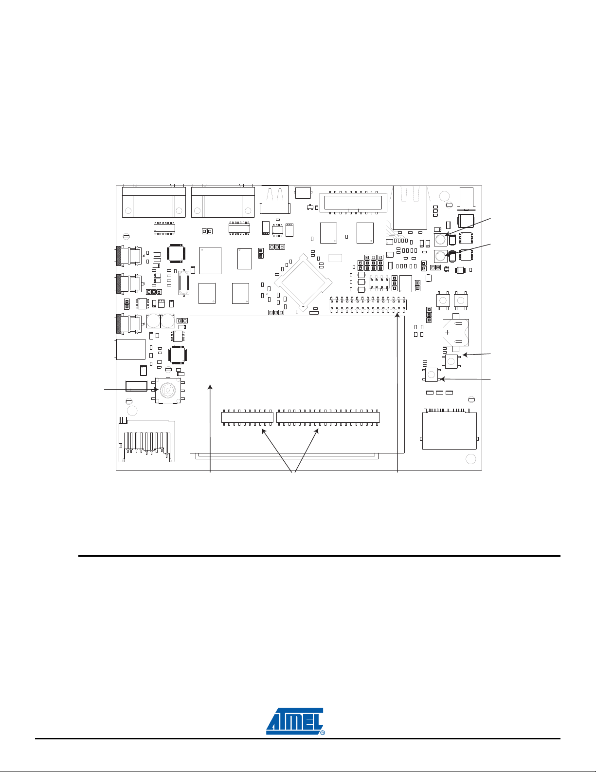
4.1.4 Display LCD and LEDs
JP15
TP4
TP2
Y6
Y7
C196
J20
J7
MN16
R72
C150
C151
J9
C118
J8
J6
R125
C199
L24
R119
C200
R121
C113
C121
JP14
R71
R68
C136
R67
J10
BP3
C192
L21
TP5
MN13
L22
C112
C146
C131
C130
C129
C137
C128
MN15
MN18
L18
MN23
C193
C144
JP13
Y3
R58
MN9
MN11
C122
JP10
J11
MN17
J18
MN8
MN10
RR13
RR17
JP6
TP6
RR9
RR11
JP9
C164
RR19
RR21
RR25
R28
C36
MN20
C163
J12
RR23
C48
R27
R26
JP5
C165
J14
M
N
5
C29
R32
R23
Q2
J23
Y2
C52
C35
C27
C54
MN6
D8
Y1
L6
R9
L3
L5
R7
R3
JP8
R25
R33
J13
J17
JP2
JP1
MN7
C172
C174
R185
R109
C177
JP11
J1
RR44
Y5
JP3
R93
R92
Y4
MN14
R107
R104
R102
R95
R94
C180
R112
C173
R143
C221
D6
D7
R11
R10
JP12
JP16
R101
R100
R108
C181
C175
C178
C171
J15
RR36
RR34
R142
C220
JP7
L7
JP4
R103
C176
C182
J5
RR35
BP5
BP2
Q1
D5
L4
D3
L2
RR46
D10
D11
D9
TP1
TP3
BP4
J3
BP1
MN4
MN2 MN1
D2
J2
C19
k
k
k
k
1
k
7
8
2
1
1
2
19
20
39
40
1
30
29
1
2
k
4
1219
20
123
1
2
1
DBGU RS232 JTAG ETHERNET
WAKE-UP
BUTTON
RESET
BUTTON
BACKUP
BATTERY
«RIGHT»
USER BUTTON
«LEFT»
USER BUTTON
SD/MMC 1
SLOT
SD/MMC 0
SLOT
USER
JOYSTICK
VIDEO
OUTPUT
HEADPHONES
HEADER
MICROPHONE
INPUT
LINE
INPUT
LCD DISPLAY LCD EXTENSION
CONNECTORS
ISI/CAMERA
CONNECTOR
POWER
HOST
USB
HOST
DEVICE
USB
Display, 480xRGBx272 pixels LCD module display connected to the PIO port E (LCD1)
One surface-mounted power red LED, user interface (D8)
Two surface-mounted green LEDs, user interface (D6 and D7)
Three surface-mounted LEDs indicate Ethernet status (D9, D10, D11)
Figure 4-2. Board Layout Commented
Board Description
4.2 Hardware Layout and Configuration
4.2.1 Processor
4.2.2 Clock Circuitry
AT91SAM9G45-EKES User Guide 4-3
The major components of the SAM9G45-EKES board are shown in Figure 4-1.
The board features the Atmel SAM9G45-CU 324-ball TFBGA package. This chip runs at a nominal frequency of 400 MHz for the core and 133 MHz for the system bus.
For more information, refer to the last SAM9G45 datasheet available from http://www.atmel.com/
The SAM9G45-EKES includes six clock sources:
6481B–ATARM–27-Nov-09
Board Description
Two are alternatives for the SAM9G45 main clock,
One crystal and one crystal oscillator are used for the Ethernet MII/RMII chip,
One crystal is used for the AC97 codec chip, and
One crystal or one crystal oscillator is used for the TV encoder.
Table 4-1. Main Components Associated with the Clock Systems
Quantity Description Component assignment
4.2.3 Reset Circuitry
1 Crystal for Internal Clock, 12 MHz Y1
1 Crystal for RTC Clock, 32.768 kHz Y2
1 Oscillator for Ethernet Clock RMII, 50 MHz Y4
1 Crystal for Ethernet Clock MII, 25 MHz Y5
1 Crystal for AC91 Codec Clock, 24.576 MHz Y3
1
Crystal for TV Encoder Clock, 13 MHz, or
Oscillator for TV Encoder, 13 MHz
Y7
Y6
The reset sources are:
Power on reset
Push button reset
JTAG reset from an in-circuit emulator interface.
4.2.4 Memory
4.2.4.1 External Memories
The SAM9G45 features a DDR2/LPDDR memory interface and an External Bus Interface (EBI) to permit
interfacing to a wide range of external memories and to almost any kind of parallel peripheral.
The SAM9G45-EKES board is equipped with DDR2/LPDDR devices featuring 128 MB of DDR2SDRAM memory (Micron MT47H64M8B6-3 16Meg*8*4).
The External Bus Interface (EBI) is connected to three kinds of memory devices:
One Parallel Flash AT49SV322DT (not populated by default)
Two DDR2-SDRAM MT47H64M8B6-3
One NAND Flash MT29F2G16ABD (not populated by default) or MT29F2G08ABD (single footprint)
The chip select NCS0, NCS1 and CS3 are used for NOR Flash, DDR2-SDRAM and NAND Flash memories, respectively. Furthermore, a dedicated jumper can disconnect each of these NCS0, NCS1, and
NCS3 signals, making them available for other functions.
4-4 AT91SAM9G45-EKES User Guide
6481B–ATARM–27-Nov-09
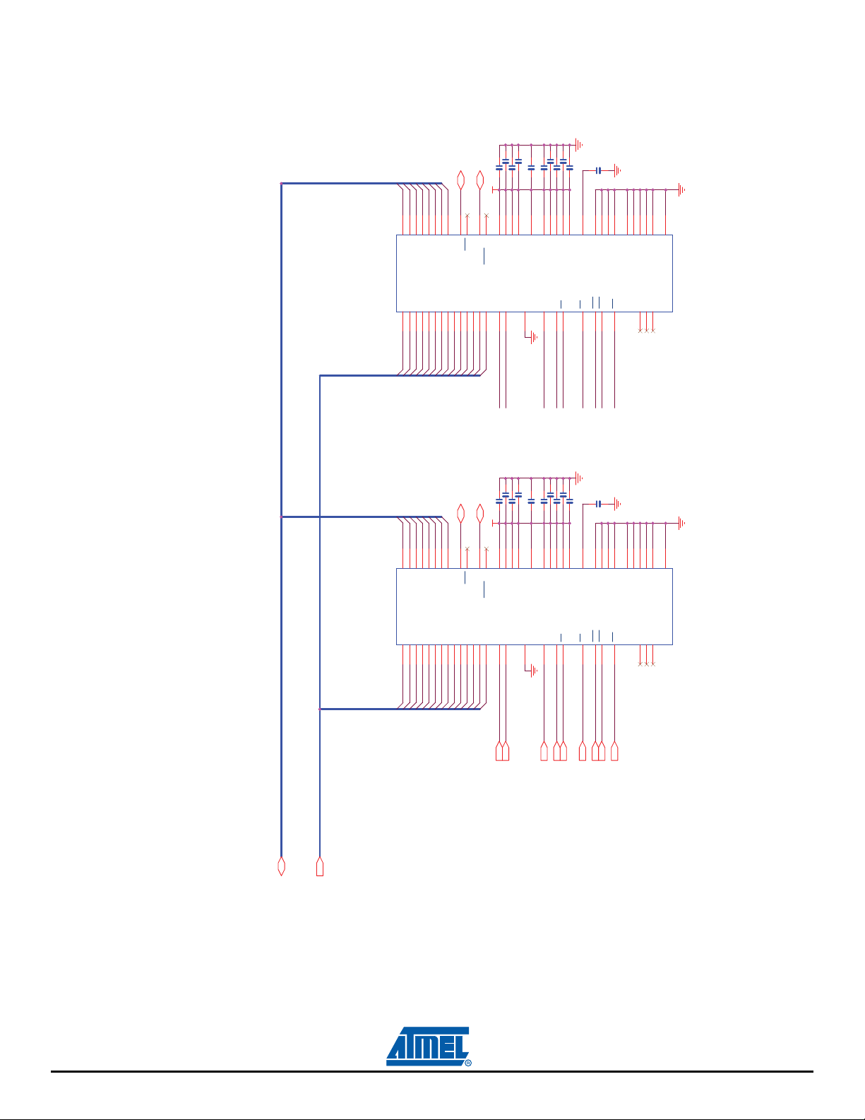
Figure 4-3. EBI0 - DDR2
MN7
MN7
DDR_D8
C8
DQ0
A0
H8
DDR_D9
DDR_D10
D7
C2
DQ2
DQ1
DDR2 S DR AM
DDR2 S DR AM
MT47H64M8CF- 3
MT47H64M8CF- 3
A2
A1
H3
H7
DDR_D11
DDR_D13
DDR_D12
D3
D1
D9
DQ4
DQ3
A4
A3
J8
J2
J3
DDR_D15
DDR_D14
B1
B9
DQ7
DQ6
DQ5
A5
A7
A6
J7
K2
A8K8A9
Board Description
C64 100nFC64 100nF
C60 100nFC60 100nF
C56 100nFC56 100nF
C58 100nFC58 100nF
C62 100nFC62 100nF
DDR_DQM1
DDR_DQS1
1V81
A8
B7
DQS
DQS
A10
K3
K7
H2
L1
E9
B3
A2
H9
A1
VDD
VDD
VDD
VDD
RDQS/NU
RDQS/DM
BA0G2ODT
A11
A13
BA1
A12
L8
L2
F9
G3
C74 100nFC74 100nF
C66 100nFC66 100nF
C70 100nFC70 100nF
C72 100nFC72 100nF
C68 100nFC68 100nF
100nF
100nF
C76
C76
DDR_VREF
C1
C7
E3
VDDQ
E2
G8
VREF
CS
G7
VSSA3VSS
RASF7WE
K9
J1
VSS
VSS
F3
E7
B8
D8
A7
B2
D2
VSSQ
VSSQ
VSSQ
VSSQ
VSSQ
VSSDL
RFU2
RFU1
RFU3
L3
L7
G1
C9
A9
C3
E1
VDDL
VDDQ
VDDQ
VDDQ
VDDQ
CKF8CAS
CKEF2CK
E8
6
6
MN
MN
DDR_A1
DDR_A0
1
0
D
D
_
_
R
DDR
DD
8
C
C2
DQ0
DQ1
DRA M
DRA M
S
S
DDR2
DDR2
A0
A1
H3
H8
_A0
_A1
R
R
DD
DD
DDR_A3
DDR_A5
DDR_A2
DDR_A4
3
5
4
DDR_D2DDR_D
DDR_D
DDR_D
7
1
3
9
D
D
D
D
DQ3
DQ2
DQ4
4M8CF- 3
4M8CF- 3
7H6
7H6
4
4
MT
MT
A3
A2
A4
3
2
J8
J
J
H7
A3
A5
R_
D
DDR_A2
DDR_
D
DDR_A4
DDR_A7
DDR_A6
6
DDR_D
DDR_D7
B1
B9
DQ5
DQ6
A6
A5
J7
K2
A7
_A6
R_
R
DD
DD
DDR_A8
DQ7
A7
K8
DDR_A8
DDR_A10
DDR_A9
R_DQS0
D
D
A8
B7
DQS
A8
A9
K3
H2
A9
R_
DDR_A10
DD
DDR_A12
DDR_A11
QM0
D
DDR_
B3
DQS
RDQS/DM
2
1
A1
A10
A1
L2
K7
1
A1
R_
DD
DDR_A12
DDR_A13
C61 100nFC61 100nF
VDD
F9
NCK
CK
CKE
C65 100nFC65 100nF
C63 100nFC63 100nF
C67 100nFC67 100nF
A9
C3
E1
C1
VDDL
VDDQ
VDDQ
ODT
CKE
8
F2
E
KE
K
C
C
KE
_C
R
DD
RAS
CS
CAS
NWE
FC69 1
F
n
n
0nFC71 100nF
0
0
0nFC73 100nF
0
0
0
0
C69 1
C73 1
C71 1
100nF
100nF
C75
C75
EF
9
7
C
A3
C
E2
E3
J1
Q
Q
D
D
DQ
VSS
VSS
VREF
VD
VD
VD
CK
CK
CS
RASF7W
CAS
8
8
F
G
G7
NCK
CAS
CS DDR_VR
RAS
K
L
K
L
S
RAS
NC
_
_
_C
_C
R
DR_CAS
DR
D
DD
D
DDR
DDR
8
2
D
B8
D
A7
K9
VSS
VSS
E
F3
NWE
DDR_WE
E7
B2
VSSQ
VSSQ
VSSQ
VSSQ
VSSQ
VSSDL
RFU2
RFU1
RFU3
7
3
1
L
L
G
BA1
BA0
C57 100nFC57 100nF
C59 100nFC59 100nF
C55 100nFC55 100nF
V8
9
2
A
H
L1
E9
A1
NU
VDD
VDD
VDD
S/
RDQ
BA0
A13
BA1
2
8
L
G
G3
13
A
R_
DD
BA1
BA0
_BA1
R
DD
DDR_BA0
]
]
5
3
.1
1
.
..
0
[0
D
R_
DD
DDR_A[
AT91SAM9G45-EKES User Guide 4-5
6481B–ATARM–27-Nov-09
Board Description
Optional 16bits DATA BUS
With AT29F2G16ABD Micron
(SDA10
)
(
SD
A10)
(NCS3)
(RDY/BSY)
(
N
ANDALE)
(NANDCLE)
WP
REWECE
RB EBI1_NAND_FSH_D6
EBI1_NAND_FSH_D0
EBI1_NAND_FSH_D3
EBI1_NAND_FSH_D4
EBI1_NAND_FSH_D2
E
BI1_NAND_FSH_D1
EBI1_NAND_FSH_D5
EBI1_NAND_FSH_D7
EBI1_NAND_FSH_D14
EBI1_NAND_FSH_D8
EBI1
_
NAND_FSH_D11
EBI1_NAND_FSH_D12
EBI1_NAND_FSH_D10
EBI1_NAND_FSH_D9
EBI1_NAND_FSH_D13
EBI1_NAND_FSH_D15
EBI1
_D
D
R
_D15
EBI1
_DDR_D11
EBI1
_D
D
R
_D
10
EBI1
_D
D
R
_D
12
EBI1
_DDR_D8
EBI1
_DDR_
D
9
EBI1
_D
D
R
_D
13
EBI1
_D
D
R
_D
14
EBI1_
DD
R_
D
7
EBI1_
D
D
R_
D
3
EBI1_
DD
R_
D
2
EBI1_
DD
R_
D
4
EBI1_
DD
R_
D
0
EBI1_
D
D
R_
D
1
EBI1_
D
D
R_
D
5
EBI1_
DD
R_
D
6
EBI1_FLASH_D4
EBI1_F
LASH
_D
2
EBI1_FLASH_D10
EBI1_FLASH_D5
EBI1_FLASH_D12
EBI1_FLASH_D9
EBI1_FLASH_D14
EBI1_FLASH_D15
EBI1_F
LASH
_D
3
EBI1_F
LASH
_D
0
EBI1_FLASH_D6
EBI1_FLASH_D7
EBI1_FLASH_D8
EBI1_F
LASH
_D
1
EBI1_FLASH_D13
EBI1_FLASH_D11
EBI1
_DDR_A2
EBI1
_DDR_A3
EBI1
_DDR_A4
EBI1
_DDR_A5
EBI1
_DDR_A6
EBI1
_DDR
_
A7
EBI1
_DDR_A8
EBI1
_DDR
_
A9
EBI1
_DDR_A1
0
EBI1
_DDR
_
A1
1
EBI1
_DDR_A1
2
EBI1
_
DD
R_
A1
3
EBI1
_
DD
R_
A1
5
EBI1
_DDR_A1
4
EBI1_
DD
R_A2
EBI1_
DD
R_
A3
EBI1_
D
D
R
_A4
EBI1_
DD
R
_
A5
EBI1_DD
R_
A6
EBI
1
_
DD
R_
A7
EB
I
1
_
DD
R_
A8
EBI1
_
DD
R_
A9
EBI1
_
D
D
R
_
A1
0
EBI1
_
D
D
R
_
A1
1
EBI1
_
DD
R
_A12
EBI1
_
DD
R
_A13
EBI1
_
DD
R
_A15
EBI1
_
DD
R
_A14
N
CL
K_
EBI1
C
S_
EBI1
BA0_EBI1
BA1_
EBI1
R
AS_
EBI1
C
AS_
EBI1
W
E_EBI1
C
KE_
EBI1
CLK_EBI
1
NC
L
K_EBI1
CS_EBI1
BA0_EBI1
BA1_EBI1
RAS_EBI1
CAS_EBI1
WE_EBI1
CKE_EBI1
VREF1
EBI1_F
L
ASH_A1
EBI
1_FL
ASH
_A2
EBI
1_FL
ASH
_A3
EBI1_FL
ASH
_A4
EBI1_FL
ASH
_A5
EBI1_FL
ASH
_A6
EBI1_FL
ASH
_A7
EBI1_F
L
ASH_A8
EBI1_F
L
ASH_A9
EBI1_F
L
ASH_A10
EBI1_FLASH_A11
EBI1_FLASH_A12
EBI1_FLASH_A15
EBI1_FLASH_A14
EBI1_FLASH_A13
EBI1_FLASH_A16
EBI1_FLASH_A18
EBI1_FLASH_A17
VREF1
VREF1
EBI1_FL
ASH
_A19
EBI1_FLASH_A20
EBI1_FLASH_A21
CLK_EBI1
A[2
.
.
1
5]
EBI1_NAND_FSH_D[0..15]
NC
L
K_
EBI1
CL
K_
EBI1
CS_
EBI1
R
AS_
EBI1
CAS_
EBI1
W
E_EBI1
CKE_
EBI1
BA1
_EBI1
BA0
_EBI1
DQS0_
EBI1
D
QM
0
_EBI1
DQS1_EBI1
DQM1_EBI1
D
[
0
.
.1
5]
_
D[
0.
.
15
]
_
A[
1.
.
21
]
EBI1_NAND
O
E
EBI1_NAND
W
E
PC14
PC8
PC4
PC5
EBI1_NRD/CFOE
EBI1_NWE/NWR0/CFWE
EBI1_NCS0
DDR_VREF
1V8
1V8
1V8
1V8
1V8
1V8
1V8
1V8 1V8
R
4
3
0R
R
4
3
0R
JP9JP9
C80 10
0
nFC80 100nF C81 100nFC81 100nF
C8
2
1
00nF
C8
2
1
00nF
C104 100nFC104 100nF
C101
10
0
nF
C101
10
0
nF
R40 470KR40 470K
MT47H64M8CF- 3
DD
R
2
S
D
RA
M
MN
8
MT47H64M8CF- 3
DD
R
2
S
D
RA
M
MN
8
A0
H
8
A1
H
3
A2
H
7
A3
J2
A4
J8
A5
J3
A6
J7
A7
K2
A8
K8
A9
K3
A10
H
2
BA0G2O
D
T
F9
DQ0
C8
DQ1
C
2
DQ2D7D
Q
3
D3
DQ4D1D
Q
5
D9
DQ6
B1
D
Q
7
B9
DQS
B7
DQS
A8
RD
Q
S/
DM
B3
RDQS/NU
A2
VDD
H9
VDD
L
1
VDDL
E1
VREF
E2
VD
DQ
C9
VSS
A3
VSS
E3
VD
DQ
A9
VDD
E9
RFU1
G1
RF
U
2
L
3
CKE
F2
CK
E8
CK
F
8
C
AS
G7
RASF7W
E
F3
C
S
G8
VD
DQ
C1
VD
DQ
C
3
VD
DQ
C7
VSSQ
B2
VSSQ
B8
VSSQ
D2
VSSQ
D
8
VDD
A1
VSS
J1
A1
1
K7
BA1
G3
A12
L2
A1
3
L8
VSS
K9
VSSDL
E7
VSSQ
A7
RFU3
L7
R39 100KR39 100K
R
42
0
R
R
42
0
R
AT4 9S V32 2DT
FLASH
CB
GA
M
N
10
DNP
AT4 9S V32 2DT
FLASH
CB
GA
M
N
10
DNP
A0E1A1
D
1
A2
C
1
A3
A1
A4B1A5
D2
A6
C2
A7
A2
A8
B5
A9
A5
A10
C5
A11
D5
A12
B6
A13A6A14C6A15D6A16E6A17B2A18
C3
RDY/ BUSY
A3
A20D3A19
D4
WEA4RESETB4OE
G1
CE
F1
VPP
B3
I/
00
E2
I
/O1
H
2
I/
O2
E3
I/O3
H3
I/
O
4
H
4
I/
O
5
E4
I/O6
H5
I/O7E5I/O8F2I/O9
G2
I/O10
F3
I/O11
G3
I/O12
F4
I/O13
G5
I/O14
F5
I/O15
G6
VCC
G4
GNDH6GND
H1
NC1
C4
NC
F6
R46 470KR46 470K
JP10JP10
C87 100nFC87 100nF
MT
2
9
F2G
08AB
D
NAND F L AS H
VF
B
GA- 6 3
MN11
MT
2
9F2G08ABDHC:D
MT
2
9
F2G
08AB
D
NAND F L AS H
VF
B
GA- 6 3
MN11
MT
2
9F2G08ABDHC:D
W
E
C7
N.C6
B9
VCC
H8
C
E
C6
R
E
D4
N.C
1
1
E3
WP
C3
N.C5
B1
N.C1
A1
N
.C2
A2
N
.C3
A9
N.C4
A10
N.C
1
2
E4
N.C13
E5
N.C14
E6
N
.C15
E7
R/B
C8
N.C17
F3
N
.
C36
M1
I/O0
H4
N.C34
L
9
N.C
2
5
L2
VSS
F7
N
.
C29
J5
VCC
J6
VSS
K3
A
L
E
C4
N.C8
D6
N.C7
B1
0
N.C
9
D7
N.C
1
0
D8
CLE
D5
N.C16
E8
N
.
C35
L10
I
/
O1
J
4
I
/
O3
K5
I
/
O2
K4
N
.
C28
H5
N.
C30
H6
N.C3
2
H
7
I/O
7
J8
I/O
6
K7
I/O5
J7
I/O4
K6
N
.
C27
J3
N
.
C26
H3
VSS
C5
N.C
2
4
L1
VSS
K8
LOCK
G
5
VC
C
D
3
VC
C
G4
N.C31
G6
N.C18
F4
N.C19
F5
N.C
2
0
F6
N.C
2
2
G
3
N.C
2
1
F8
N.C3
3
G7
N.C
2
3
G
8
N
.
C37
M2
N
.
C38
M9
N
.
C39
M10
C94 1
0
0nFC94 100nF
C93 100nFC93 100nF
R451KR45
1K
MT47H64M8CF- 3
DDR2 S D
R
A
M
MN
9
MT47H64M8CF- 3
DDR2 S D
R
A
M
MN
9
A0
H
8
A1
H
3
A2
H
7
A3
J
2
A4
J
8
A5
J
3
A6
J
7
A7K2A8K8A9K3A1
0
H2
BA0
G
2
ODT
F9
D
Q0
C8
DQ1
C2
D
Q2
D7
D
Q3
D3
D
Q
4
D1
D
Q
5
D9
D
Q6
B1
DQ7
B9
DQS
B7
DQS
A8
RDQS/DM
B3
RDQS/NU
A2
VDD
H9
VDD
L1
VDDL
E1
VREF
E2
VDDQ
C9
VSS
A3
VSS
E3
VDDQ
A9
VDD
E9
RFU1
G
1
RFU2
L
3
CKEF2CKE8CK
F
8
CASG7RASF7WE
F3
CS
G
8
VDDQ
C
1
VDDQ
C3
VDDQ
C7
VSSQ
B2
VSSQ
B8
VSSQ
D2
VSSQ
D8
VDD
A1
VSS
J1
A1
1
K7
BA1
G
3
A1
2
L
2
A13
L
8
VSS
K9
VSSDL
E7
VSSQ
A7
RFU3
L
7
R41
470K
R41
470K
C83 100nFC83 100nF
C92 1
0
0
n
FC92 1
0
0
n
F
C95 100nFC95 100nF
C88 100nFC88 100nF
C103 100nFC103 100nF
C90 1
0
0
n
FC90 1
0
0
n
F
C100
100nF
C100
100nF
C106 100nFC106 100nF
C89 100nFC89 100nF
R4
7
DNP
R4
7
DNP
C102
100nF
C102
100nF
C96 1
0
0nFC96 100nF
R440RR44
0R
C97 100nFC97 100nF
C99 100nFC99 100nFC98 100nFC98 100nF
C105 100nFC105 100nF
C91 100nFC91 100nF
C8
6 100nFC86 100nF
C84 100nFC84 100nF C85 100nFC85 100nF
Figure 4-4. EBI1 - DDR2 + Flash
4-6 AT91SAM9G45-EKES User Guide
6481B–ATARM–27-Nov-09

4.2.5 Power Supplies
The SAM9G45 Board contains four regulated power supplies:
3.3 VDC Supply
1.8 VDC Supply
1.0 VDC Core Supply
1.0 VDC Core UTMI Supply, PLL
The outputs of these regulated power supplies1 are distributed as necessary to each part of the circuit
board.
The 3.3 VDC Supply is generated by an LTC1765-3.3 chip. It accepts VIN 5 VCC power and outputs a
regulated +3.3 V to most other circuits in the SAM9G45-VB.
The 1.8 VDC Supply (VDDIOM0, VDDIOM1) is generated by an LT1765-1.8. It is powered by VIN
5 VCC power and outputs a regulated +1.8V.
The 1.0 VDC Core Supply (VDDCORE) is generated by a TPS60500 IC. It is powered by the VIN
5 VCC power.
The 1.0 VDC Core Supply (VDDUTMIC, VDDPLLUTMI and VDDPLLA) is generated by a CMOS
voltage regulator R1100D series. It is powered by the output of the 3.3 VDC Supply.
Board Description
Note: 1. Corresponding test points (TP1 to TP4, GND) are used with jumpers (JP1.1 to JP7) to
permit probing of these voltages.
AT91SAM9G45-EKES User Guide 4-7
6481B–ATARM–27-Nov-09
Board Description
FO
R
CE
P
O
WER
O
N
1V VDDUTMIC
VDDBU
VDDUTMIC
SHD
N
VDDPLLUTMI
VDDPLLA
VDDBU
VDDCORE
V
D
DUTMI
I
VDD
A
NA
VDDOSC
VDDIOP0
VDDIOP1
VDDIOP2
VDDISI
VDDIOM0
VDDIOM1
1V
3
V3
5
V
1
V8
5
V
5
V
3V3
3V
3
1V
1V8
3V3
L
3
10uH150mA
L
3
10uH150mA
JP3JP3
1
2
3
R4
1
0
K
R4
1
0
K
C41
0
uF
C41
0
uF
C182
.2
u
F
C182
.2
u
F
C10
2.2uF
C10
2.2uF
R6
68KR668K
J1-2J1-2
3 4
C62.2nF
C62.2nF
C1
9
1
0pF
C1
9
1
0pF
C15
2.2nF
C15
2.2nF
C17
1uF
C17
1uF
C24
4.7uF
C24
4.7uF
JP4JP4
J1-3J1-3
5 6
L2
2.2uHL22.2uH
C8
4.7uFC84.7uF
C
16
1uF
C
16
1uF
C14
2.2uF
C14
2.2uF
C2
2
.
2u
F
C2
2
.
2u
F
L
1
1
0u
H
1
50
m
A
L
1
1
0u
H
1
50
m
A
MN3
R1100D101C
MN3
R1100D101C
OUT
1
VDD
2
GND
3
M
N
1
L
T
1
76
5
-
3
.3
M
N
1
L
T
1
76
5
-
3
.3
GND1
1
BOOST
2
SYNC
14
SHD
N
1
1
VI
N1
3
GND2
8
GND4
9
GND5
16
VIN
2
4
SW25SW1
6
NC
1
7
NC3
15
VC
13
FB
1
2
NC
2
10
GND3
17
D3
ST
PS
2
L
30A
D3
ST
PS
2
L
30A
JP2JP2
1
2
3
C1
1
8
0nF
C1
1
8
0nF
J
2
2
.1
MM SOCKET
J
2
2
.1
MM SOCKET
1
2
3
L5
10uH150mAL510uH150mA
C20
100nF
C20
100nF
R31RR3
1R
C25
100nF
C25
100nF
C5
4
.
7u
F
C5
4
.
7u
F
JP5JP5
1
2
3
J3J3
MN2
LT
1
765-1.8
MN2
LT
1
765-1.8
GND1
1
BOOST
2
SYNC
14
SHDN
1
1
VIN1
3
GND2
8
GND4
9
GND5
16
VIN2
4
SW
2
5
SW
1
6
N
C1
7
NC3
15
VC
13
FB
1
2
NC2
10
GND3
17
J1-4J1-4
7 8
C3100nF
C3100nF
C13
2.2uF
C13
2.2uF
R91RR9
1R
JP6JP6
1
2
3
C9
180nFC9180nF
L4
2.
2
uH
L4
2.
2
uH
R5
1
0
K
R5
1
0
K
D5
STPS2
L
30A
D5
STPS2
L
30A
JP1JP1
1
2
3
R11R
R11R
J1-1J1-1
1 2
C21
4.7uF
C21
4.7uF
D1
BA
T
20J
D1
BA
T
20J
21
D4
BAT20JD4BAT20J
21
R8
220
K
R8
220
K
L6
10uH150mAL610uH150mA
M
N4
TPS
6
0500
M
N4
TPS
6
0500
C1M
8
GND
9
VOUT
7
EN
1
VIN
5
C
1
P
6
C2M
3
C2P
4
FB
10
PG
2
Q1
Si1563EDHQ1Si1563EDH
132
4
5
6
C23
100nF
C23
100nF
JP7JP7
1
2
3
C710
0n
F
C710
0n
F
C1
1
1
5
pF
C1
1
1
5
pF
R2
1
00K
R2
1
00K
R71RR7
1R
D2
5
V
D2
5
V
C22
22uF
C22
22uF
C12
10uF
C12
10uF
Figure 4-5. Power Supply and Management Power Block
4-8 AT91SAM9G45-EKES User Guide
6481B–ATARM–27-Nov-09

4.2.6 Debug Interface
ICE INTERFACE
TDI
R
TCK
TDO
TMS
TC
K
NTRST
NRST
TC
K
TMS
TDI
NTRST
NRST
TDO
R
TCK
3
V3
3
V3
3
V3
R85 0RR85 0R
R87
DN
P
R87
DN
P
R86
0
R
R86
0
R
R84 DNPR84 DNP
RR42
100K
RR42
100K
15234
678
J13J13
12
3
4
5
6
7
8
9
10
11
12
13
15
17
19
14
16
18
20
SERI
AL DEBUG PORT
PB12
PB13
3V3
3V3
C156
100nF
C156
100nF
R830RR830R
C158
100n
F
C158
100n
F
C155
100n
F
C155
100n
F
J1
0
MAL
E R
IGHT ANG
LE
J1
0
MAL
E R
IGHT ANG
LE
5
4
3
2
1
9
8
7
6
10
11
C1+
V
+
VCC
C1-
C2+
C2-V
-
T
T
R
R
G
ND
MN18
ADM3202ARNZ
C1+
V
+
VCC
C1-
C2+
C2-V
-
T
T
R
R
G
ND
MN18
ADM3202ARNZ
116
3
4
5
15
1
1
10
12
98
13
7
1
4
2
6
R8
0
100K
R8
0
100K
C153
100nF
C153
100nF
C160
100nF
C160
100nF
R8
2
100
K
R8
2
100
K
4.2.6.1 JTAG/ICE
Software debug is accessed by a standard 20-pin JTAG connection. This allows connection to a standard USB-to-JTAG in-circuit emulator.
Figure 4-6. JTAG Interface
Board Description
4.2.6.2 DBGU Com Port
This UART is connected to the DB-9 male socket through an RS-232 Transceiver (TXD and RXD only).
Figure 4-7. DBGU Com Port
AT91SAM9G45-EKES User Guide 4-9
6481B–ATARM–27-Nov-09
Board Description
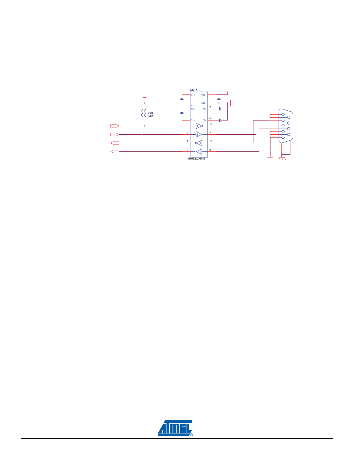
4.2.6.3 User Serial Com Port
The USART1 is used as a user serial com port. This USART1 is buffered with an RS-232 Transceiver
(TXD, RXD and handshake CTS/RTS control) and connected to the DB-9 male socket. Software must
assign the appropriate PIO pins (PB5 = RXD1, PB4 = TXD1, PD16 = RTS1, PD17 = CTS1) to enable the
UART1 function.
Figure 4-8. User Serial Com Port
Refer to the SAM9G45 datasheet for more information about the SAM9G45 USARTs.
P
PD16
PB5
PD17
3
MN17
MN17
1 16
C1+V+VCC
F
F
C1+V+VCC
GN
GN
3
C1-
C1-
4
C2
C2
+
+
5
C2
C2
-V
-V
11
T
T
1
0
T
T
1
2
R
R
9 8
R
R
ADM3202ARNZ
ADM3202ARNZ
D
D
-
-
3V3
R79
R79
R81
R81
100
100
100K
100K
K
K
B4
C152
C152
100nF
100nF
C159
C159
100n
100n
3V
C154
C154
100nF
100nF
15
2
6
14
7
13
C157
C157
100nF
100nF
C161
C161
100n
100n
F
F
RS232 COM PORT
MALE RIGHT ANGLE
MALE RIGHT ANGLE
1
6
2
7
3
8
4
9
5
10
11
J11
J11
4.2.6.4 USB Port
The SAM9G45-EKES features USB communication ports:
Two Host Ports: Full speed OHCI and High speed EHCI
One Device Port: High speed.
USB Host Port0 is directly connected to the first UTMI transceiver. The second Host Port (Port1) is multiplexed with the USB device High speed and connected to the second UTMI port.
One USB high/full speed type standard A connector
One USB interface Host/Device Micro AB connector
Refer to the SAM9G45 datasheet for detailed programming information.
4-10 AT91SAM9G45-EKES User Guide
6481B–ATARM–27-Nov-09
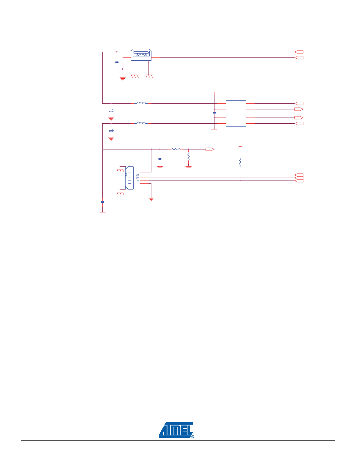
Figure 4-9. USB Port
USB HOST/DEVICE IN
TERFAC
E
USB HOST INTERFAC
E
(
ENA
)
(
ENB)
(FLGA)
(FLGB
)
(VBU
S)
(IDUSB)
H
DMA
H
DPA
HDMB
HDPB
PD28
PB
19
PD3
PD2
PD4
PD1
5V
3V3
L
1
5
BLM21PG221SN1x
L
1
5
BLM21PG221SN1x
C166
1
0pF
C166
1
0pF
R8847KR884
7K
C163
1
00n
F
C163
1
00n
F
L1
6
BLM21PG221SN1x
L1
6
BLM21PG221SN1x
R89
68
K
R89
68
K
MN20
SP2526A-
2
MN20
SP2526A-
2
ENA
1
FLGA
2
ENB
4
OUTA
8
GNG6FLG
B
3
IN
7
OUTB
5
J12
292303-1
J12
292303-1
1
4
5
2
3
6
R9
0
47K
R9
0
47K
C165
1
6V
33 uF
C165
1
6V
33 uF
C164
16V
33 u
F
C164
16V
33 u
F
VBUS
SHD
DM
DP
ID
GND
J14
ZX6
2-AB-5P
VBUS
SHD
DM
DP
ID
GND
J14
ZX6
2-AB-5P
1
2
3
4
5
7
6
C16
2
100nF
C16
2
100nF
C167
100n
F
C167
100n
F
Board Description
4.2.6.5 Ethernet 10/100 (EMAC) Port
The port is compatible with IEEE® Standard 802.3.
The SAM9G45-EKES is equipped with a Davicom DM9161AEP 10/100 Mbps Fast Ethernet Physical
Layer TX/FX Single Chip Transceiver. It contains the entire physical layer functions of 100BASE-TX as
defined by IEEE 802.3u, including the Physical Coding Sublayer (PCS), Physical Medium attachment
(PMA), Twisted Pair Physical Medium Dependent Sublayer (TP-PMD), 10BASE-TX Encoder/Decoder
(ENC/DEC), and Twisted Pair Media Access Unit (TPMAU).
The Ethernet interface integrates an RJ45 connector with an embedded transformer, and three status
LEDs.
The Ethernet interface provides two selectable modes, MII or RMII (Reduced MII), for 100Base-Tx or
10Base-Tx. The MII and RMII interfaces are capable of both 10Mb/s and 100Mb/s data rates as
described in the IEEE 802.3u standard. The signals used by MII and RMII interfaces are described in the
6481B–ATARM–27-Nov-09
table below.
AT91SAM9G45-EKES User Guide 4-11

Board Description
Table 4-2. Pin Mapping for Normal MII and Reduced MII
Pin Name Normal MII Mode Reduced MII Mode
SAM9G45 DM9161 SAM9G45 DM9161
ETX0-ETX1 ETX[0:1] transmit data TXD [0:1] ETX[0:1] TXD [0:1]
ETX2-ETX3 ETX[2:3] transmit data TXD [2:3] NC NC
ETXEN ETXEN: transmit enable TXEN ETXEN: transmit enable TXEN
ETXER ETXER: transmit error TXER/TXD[4] NC NC
ETXCK/REFCK ETXCK: transmit clock TXCLK REFCK: reference clock REF_CLK
ERX0-ERX1 ERX[0:1]: receive data RXD [0:1] ERX[0:1]: receive data RXD [0:1]
ERX2-ERX3 ERX[2:3]: receive data RXD [2:3] NC NC
ERXER ERXER: receive error
ERXDV ERXDV: receive valid data RXDV
RXER/RXD[4]/
RPTR/NODE
ERXER: receive error RPTR/NODE
ECRSDV: carrier sense /
data valid
CRS DV
ERXCK ERXCK: receive clock RXCLK NC NC
ECOL ECOL: collision detect COL NC NC
ECRS
EMDC EMDC: management data clock MDC
EMDIO
NRST NRST: microcontroller reset
ECRS: carrier sense /
data valid
EMDIO: management data
input / output
CRS (PHYAD[2:4] NC NC
MDIO
RESET# XT1
(25 MHz)
EMDC: management data
clock
EMDIO: management data
input / output
NRST: microcontroller reset
MDC
MDIO
RESET# XT1
(REF_CLK 50MHz)
4-12 AT91SAM9G45-EKES User Guide
6481B–ATARM–27-Nov-09
 Loading...