


AT91SAM9G10-EK Evaluation Board
....................................................................................................................
User Guide
6479A–ATARM–26-May-09

1-2 AT91SAM9G10-EK Evaluation Board User Guide
6479A–ATARM–26-May-09

AT91SAM9G10-EK Evaluation Board
User Guide
Section 1
Overview.....................................................................................................................1-1
1.1 Scope ................................................................................................................................. 1-1
1.2 Deliverables ....................................................................................................................... 1-1
1.3 The AT91SAM9G10-EK Evaluation Board ........................................................................ 1-1
Section 2
Setting Up the AT91SAM9G10-EK
Evaluation Board ........................................................................................................2-1
2.1 Electrostatic Warning ......................................................................................................... 2-1
2.2 Requirements..................................................................................................................... 2-1
2.3 Layout ................................................................................................................................ 2-2
2.4 Powering Up the Board ...................................................................................................... 2-4
2.5 Backup Power Supply ........................................................................................................ 2-4
2.6 Getting Started ................................................................................................................... 2-4
2.7 AT91SAM9G10-EK Block Diagram.................................................................................... 2-5
Section 3
Board Description .......................................................................................................3-1
3.1 AT91SAM9G10 Microcontroller ......................................................................................... 3-1
3.2 AT91SAM9G10 Block Diagram.......................................................................................... 3-4
3.3 Memory .............................................................................................................................. 3-5
3.4 Clock Circuitry .................................................................................................................... 3-5
3.5 Reset Circuitry.................................................................................................................... 3-5
3.6 Shutdown Controller........................................................................................................... 3-5
3.7 Power Supply Circuitry.......................................................................................................3-5
3.8 Remote Communication..................................................................................................... 3-5
3.9 Audio Stereo Interface .......................................................................................................3-5
3.10 User Interface..................................................................................................................... 3-6
3.11 Debug Interface.................................................................................................................. 3-6
3.12 Expansion Slot ................................................................................................................... 3-6
3.13 PIO Usage ......................................................................................................................... 3-7
Section 4
Configuration Straps...................................................................................................4-1
4.1 Configuration Straps .......................................................................................................... 4-1
Section 5
Schematics .................................................................................................................5-1
5.1 Schematics......................................................................................................................... 5-1
AT91SAM9G10-EK Evaluation Board User Guide 2-1
6479A–ATARM–26-May-09

Section 6
Errata..........................................................................................................................6-1
6.1 JTAGSEL S5 Footprint Selector ........................................................................................ 6-1
6.2 External Capacitor Values on XIN and XOUT.................................................................... 6-1
Section 7
Revision History..........................................................................................................7-1
7.1 Revision History ................................................................................................................. 7-1
2-2 AT91SAM9G10-EK Evaluation Board User Guide
6479A–ATARM–26-May-09
1.1 Scope
The AT91SAM9G10-EK evaluation kit is an effective platform for evaluating chip performance and
developing code for applications based on the AT91SAM9G10.
This guide is a description of the hardware included in the AT91SAM9G10-EK evaluation kit. Software
files are available embedded into the board’s memory upon delivery.
1.2 Deliverables
The AT91SAM9G10-EK package contains the following items:
an AT91SAM9G10-EK board
one A/B-type USB cable
one serial RS232 cable
one RJ45 crossed Ethernet cable
universal input AC/DC power supply with US and EU plug adapter
Section 1
Overview
1.3 The AT91SAM9G10-EK Evaluation Board
The board is equipped with an AT91SAM9G10 (217-ball LFBGA package) together with the following:
64 Mbytes of SDRAM memory
256 Mbytes of NAND Flash memory
one Atmel
one USB device port interface
two USB host port interfaces
one DBGU serial communication port
JTAG/ICE debug interface
one Ethernet 100-base TX with three status LEDs
one Atmel AT73C213 Audio DAC
one 3.5" 1/4 VGA TFT LCD Module with TouchScreen and backlight
one Power LED and two general-purpose LEDs
four user input pushbuttons
one wakeup input pushbutton
one reset pushbutton
one DataFlash SD/MMC card slot
®
serial DataFlash
®
AT91SAM9G10-EK Evaluation Board User Guide 1-1
6479A–ATARM–26-May-09

two expansion footprint connectors (solder side)
one Lithium Coin Cell Battery Retainer for 12 mm cell size
dual pitch prototyping area
1-2 AT91SAM9G10-EK Evaluation Board User Guide
6479A–ATARM–26-May-09

2.1 Electrostatic Warning
The AT91SAM9G10-EK evaluation board is shipped in a protective anti-static package. The board must
not be subjected to high electrostatic potentials. In risky ESD environments (e.g. offices with carpet) a
grounding strap or similar protective device should be worn when handling the board. Also, generally
avoid touching the component pins or any other metallic element of the board.
2.2 Requirements
In order to set up the AT91SAM9G10-EK evaluation board, the following items are required:
the AT91SAM9G10-EK evaluation board itself
AC/DC power adapter (5V at 2A), 2.1 mm by 5.5 mm
Section 2
Setting Up the AT91SAM9G10-EK
Evaluation Board
AT91SAM9G10-EK Evaluation Board User Guide 2-1
6479A–ATARM–26-May-09
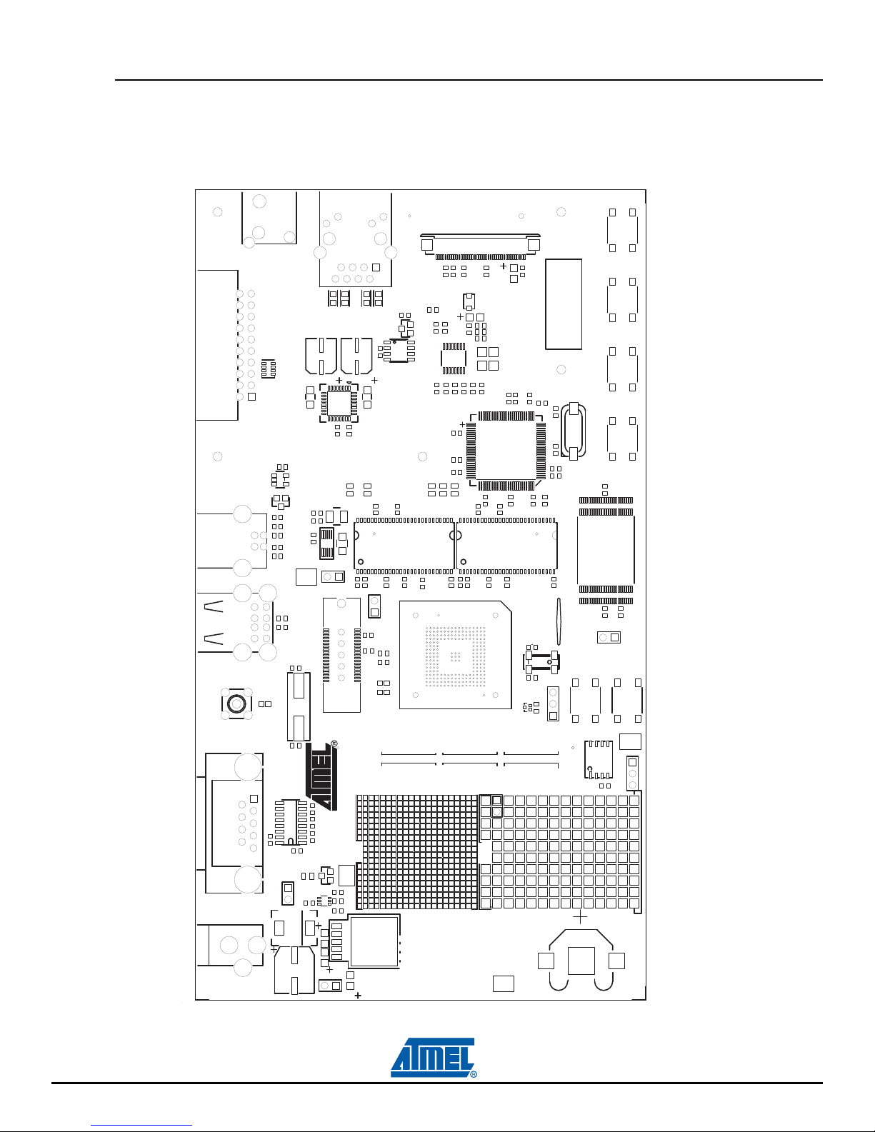
2.3 Layout
C112
R30
R29
BP5
C124
C125
R72
L5
C84
R83
R82
R75
J13
19
20
1
C115
J23
1
J20
BP6
J10
TP2
C4
J2
C3
1
C1
R6
1
MN1
C9
C2
R2
CR1
J1
TP1
R5
Q2
Q1
J3
DS1
k
1
C91
C93
C92
R20
C95C94
MN13
1
J21
1
TP4
MN7
C16
J15
J7
BP2
BP1
MN10
J9
J24
C126
1
S7
S9
Y1
Y2
C20
R12
S8
C17
J18
J4
1
C19
MN3
R11R9C11
1
1
R55
A4
B4
MN6B
R19
C59
11
C52
A1
C45
C56
J8
J5
J12
1
R54
A1
B1
MN6A
MN4
C51
C46
C53
R18
C55
C49
MN5
C57
C48
1
TP3
R63
MN2
C10
R66
R65
R64
R62
R4
R3
C60
R32
R28
R27
C68
C44
DS4
C50
DS3
DS2
C47
DS8
DS7
C54
C7
MN14
C8
Q5
J19
R34
C69
1
R23
k
k
k
C72
k
k
C110
C102
BP3
C67
C66
MN8
C70
C111
R68
MN15
J6
Y3
R31
C74
C75
C73
R81
R80
R78
R77
R76
R73
C107
RR1
1
2
BP4
TP66
TP65
TP64
TP63
1
MN16
MN11
1
C123
C122
C121
C120
R79
R84
R74
Q6
C113
R26
R25
C87
GND
3.3V
5V ONLY
WARNING
GND
1
POWER
FORCE
3.3V
3.3V
LED
POWER
ON
GND
5V
3.3V
5V
0
GND
DATAFLASH
PORT B
201612
181410
864
2
2
GND
28
24
4
0
302622
PORT A
221814
10
6
242016
12
8
840
30
26
6
2
GND
28
PORT C
2824201612
2622181410
3.3V
VDDBU
NRST
GND
GND
GND
GND
NC
30
5V
PORT
DEBUG
SERIAL
GND
GND
1
211713
9
191511
7
5
3
3
29
25
5
1
1
312723
GND
231915
11
7
252117
13
9
9
5
1
31
27
7
3
29
GND
2925211713
2723191511
NC
31
WKUP
SHDN
3.3V
GND
GND
GND
GND
5V
EXT. CLOCK
1.2V
BB
VDDBU
ETM TRACE PORT
UP
WAKE
RESET
USB HOST INTERFACE
SELECT
BOOT MODE
VDDOSC+VDDPLL
1.2V
NANDFLASH
VDDCORE
USB DEVICE INTERFACE
SPEED
DUPLEX
FULL
ACT
&
LINK
TOUCH SCREEN
CONTROLLER
CONNECTOR
JTAG/ICE
AT91SAM9261-EK
10/100
ETHERNET
AUDIO OUT
STUDIEL
WWW.STUDIEL.FR
Figure 2-1. AT91SAM9G10-EK Layout - Top View
2-2 AT91SAM9G10-EK Evaluation Board User Guide
6479A–ATARM–26-May-09
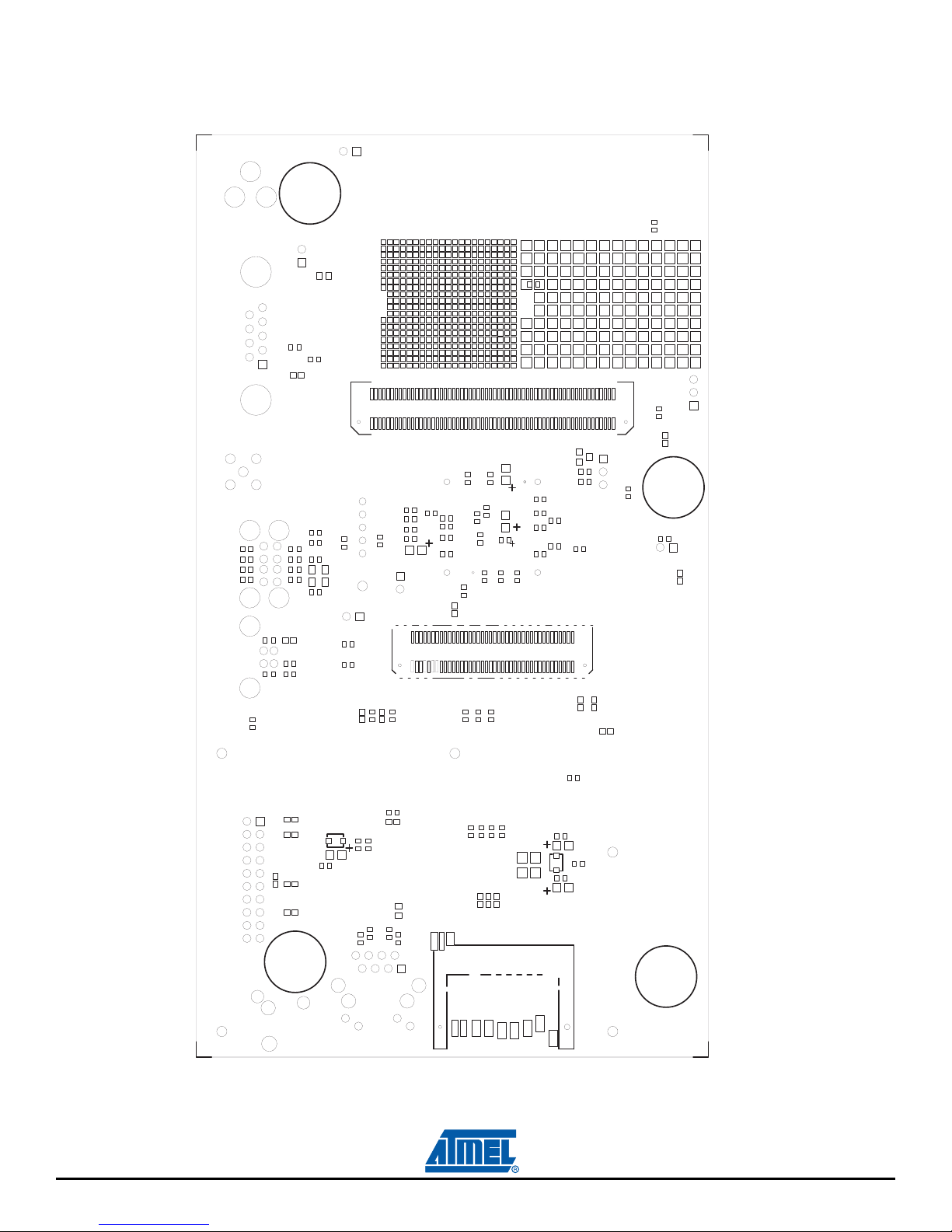
Figure 2-2. AT91SAM9G10-EK Layout - Bottom View
R1
R52
R15
R85
R53
S21
R60
C100
C101
R61
R70
R56
C96
C97
R57
C104
S22
C105
C106
C103
S5
S2
S6
S3
S4
119
120
C38
C40
C14
C39
C18
C15
C13
R59
R10
R58
C99
F2
F1
C98
L4
C114
R69
C64
C12
R8
C6
J17
C5
S19
S20
R51
R50
R67
S23
C109
C108
C63
C62
C21
C42
C28
C41
C35
S10
79
80
R21
C119
L1
C61
C43
C25
C27
C23
C24
C26
C34
C33
R22
R24
C117
C116
C118
S26
S25
S24
CR2
C36
C37
C22
C31
C30
C29
C32
1
2
S14
C79
L2
C77
C76
J22
1
C58
J16
2
S12
R17
R16
R13
R7
R14
S13
S15
S16
C71
C78
R71
AT91SAM9G10-EK Evaluation Board User Guide 2-3
INTERFACE
DATAFLASH CARD
SD CARD/MMC CARD
6479A–ATARM–26-May-09

2.4 Powering Up the Board
AT91SAM9G10-EK requires 5V DC (±5%). DC power is supplied to the board via the 2.1 mm by 5.5 mm
socket (J1). The coaxial power plug center pin is positive polarity.
2.5 Backup Power Supply
The user has the possibility to add a battery (3V Lithium Battery CR1225 or equivalent) in order to permanently power the backup part of the device. In this case, J9 configuration must to be set in position 1,
2.
Refer to Table 4-1, “Configuration Jumpers and Straps”.
2.6 Getting Started
The AT91SAM9G10-EK evaluation board is delivered with an embedded demo and documentation files
allowing the user to begin evaluating the AT91 ARM Thumb 32-bit microcontroller quickly. Simply power
the board and connect it to the USB port of your PC to open it. Also, please refer to the AT91 web site,
www.atmel.com/products/AT91/, for the most up-to-date information on getting started with the
AT91SAM9G10-EK.
2-4 AT91SAM9G10-EK Evaluation Board User Guide
6479A–ATARM–26-May-09
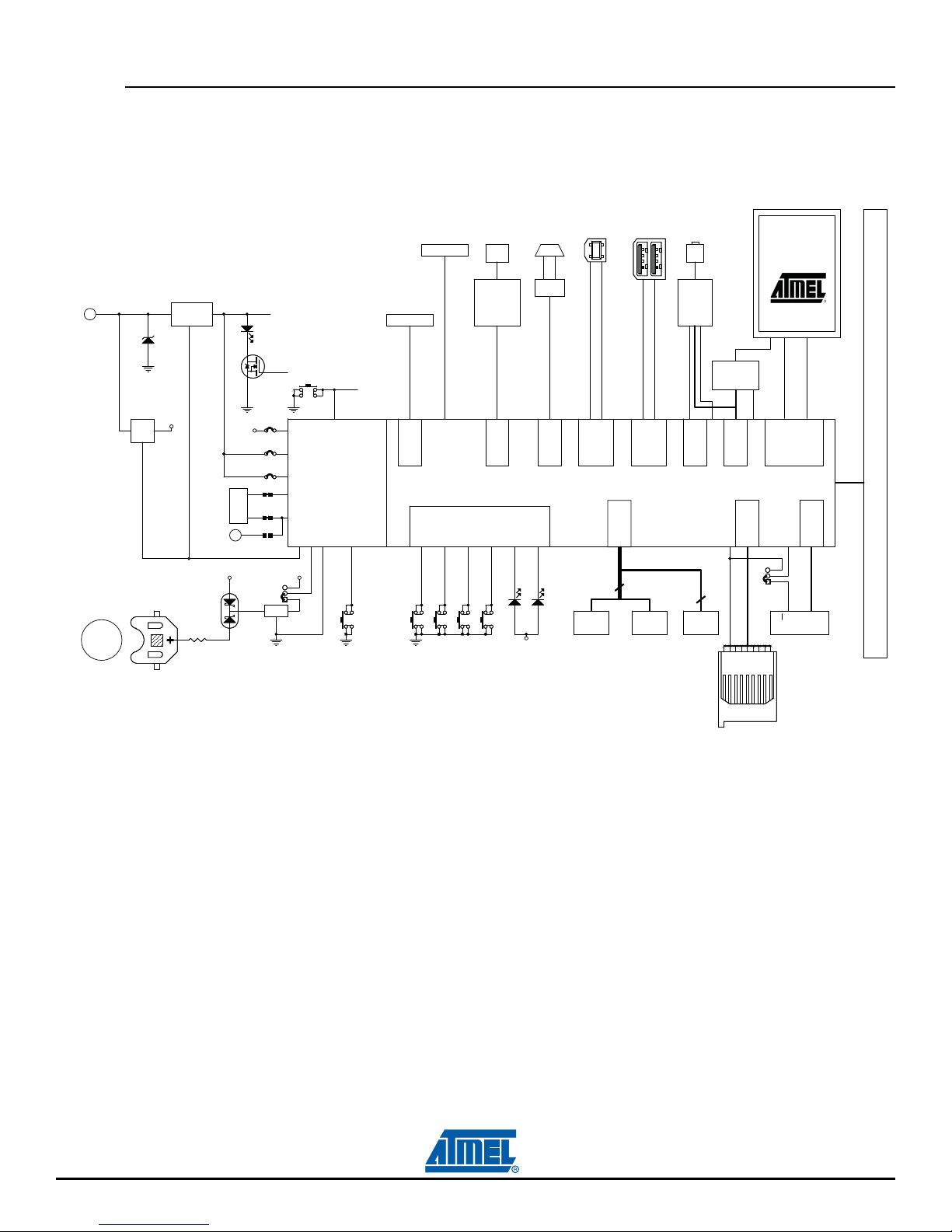
2.7 AT91SAM9G10-EK Block Diagram
Figure 2-3. Block Diagram
POWER SUPPLY
5 VDC
3V
+
REG
1V2
SHUTDOWN
LINEAR REGULATOR
3V3
5V5V
SHUTDOWN
1V2
1V2
18.432 MHz
EXT CLK INPUT
3V3
VDD3V3
YELLOW POWER LED
PIO
1.2V
VDDCORE
VDDPLL VDDOSC
VDDIO
SYSTEM CONTROLLER
XOUT
XIN
SHDN
VDDBU
1V2
3
2
1
NRST
NRST
TRACE PORT
ETM
PA11..PA31
JTAG/ICE
ETHERNET 10/100
RJ45
EMAC + PHY
EBI
DBGU
RS232
TXD
ADM3202A
DRXD - DTXD
DBGU
HEADPHONE
OUT
RXD
DDP
USB DEVICE
AT73C213
STEREO
AUDIO DAC
TOUCHSCREEN
CONTROLLER
SCC1 I2S
HDMB - HDPB
HDMA - HDPA
DDM
SPI0
SCC1
USB HOST
PA29 / SPI0_NPCS3
1/4 VGA DISPLAY
WITH TOUCHSCREEN
LCD CONTROLLER
SPI0_NPCS2
TFT
320 x 240
LCD CONTROL
AT91SAM9G10
SDRAM
256 Mb
EBI
32
16
SDRAM
256 Mb
16
8
NANDFLASH
MCI
SPI0_NPCS3 / PA6
85 7643219
3
2
1
SPI0_NPCS0
CS
DATAFLASH
DEVICE
SPI0
EXPANSION CONNECTORS
MISO - MOSI - SPCK
PIO
WKUP
GNDBU
3V3
USER'S GREEN LED
SD/MMC
DATAFLASH
CARD READER
AT91SAM9G10-EK Evaluation Board User Guide 2-5
6479A–ATARM–26-May-09

2-6 AT91SAM9G10-EK Evaluation Board User Guide
6479A–ATARM–26-May-09
 Loading...