

Page 1
Service Manual
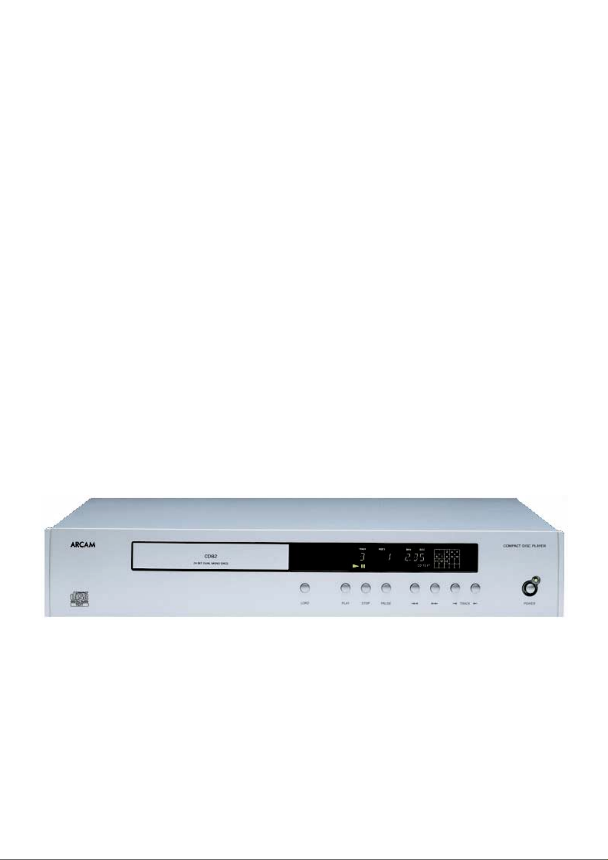
ARCAM
CD82
Issue 1.0
DiVA CD82
Compact Disc Player (Text)
ARCAM
Page 2

Contents List
Section Issue
Service guide
! Technical specification -
!
CD82 upgrad e instructions -
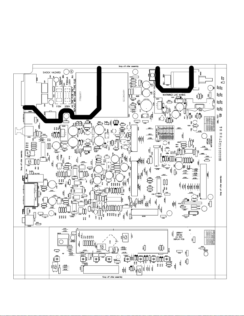
Main board L934
! Circuit description -
! Component overlay 5.0
! Parts list 4.1
! Circuit diagrams 4.1
DAC board L949
! Component overlay 3.0
! Parts list 3.05
! Circuit diagrams 3.0
Mechanical
Mechanical parts list -
Page 3

Service Guide
Contents
!
Technical
specification
!
CD82 Upgrade fitting
instructions
Page 4

CD82 Technical Specifications
Digital to Analogue conversion
DAC Dual mono 24 bit Wolfson
Laser pick-up 3 beam
Laser wavelength 780nm
Numeric aperture 0.45
Dynamic range 106dB
Signal to noise ratio (CCIR) >100dB
Harmonic distortion (0dB, 1kHz) <0.005%
Frequency response (+-0.5dB) 5Hz-20kHz
Output level (0dB) 2.3Vrms
Output impedance 50 ohm
Minimum recommended load 5k ohm
General
Digital output connection 75 ohm co-axial
Power consumption 35VA
Dimensions (including feet) W430 x D290 x H84mm
Weight (net) 5.5kg
Weight (packed) 7.0kg
Supplied accessories Mains lead
CR314 remote control
2 x AAA batteries
Page 5

DiVA CD82 UPGRADE FITTING
INSTRUCTIONS
Compatible with:
Alpha 7, 7SE, 8, 8SE CD players
DiVA CD72, CD72 (text) CD players
Note – When converting from 8SE to CD82 you will no
longer be able to decode the extra information on the few
HDCD discs available, however the sound quality offered by
the CD82 upgrade is significantly superior on all discs to
that of the original 8SE.
Kit Contents
1x CD82 DAC module L951AY
1x Upgrade instruction sheet E836UI
1x Silver CD82 drawer front assembly E993AY
1x Black CD82 drawer front assembly E993AYB
2x PCB support locking pillars H037
5x Self tapping screws HF4V09B
1x Product registration card SH000
1x CD82 authentication label E954SL
1x Surface cleaner wipe F227
Upgrading an Alpha 7/7SE, 8/8SE to CD82 DAC
For 7/7SE follow steps 1,2,3A onwards (not 3B)
For 8/8SE follow steps 1,2,3B onwards (not 3A)
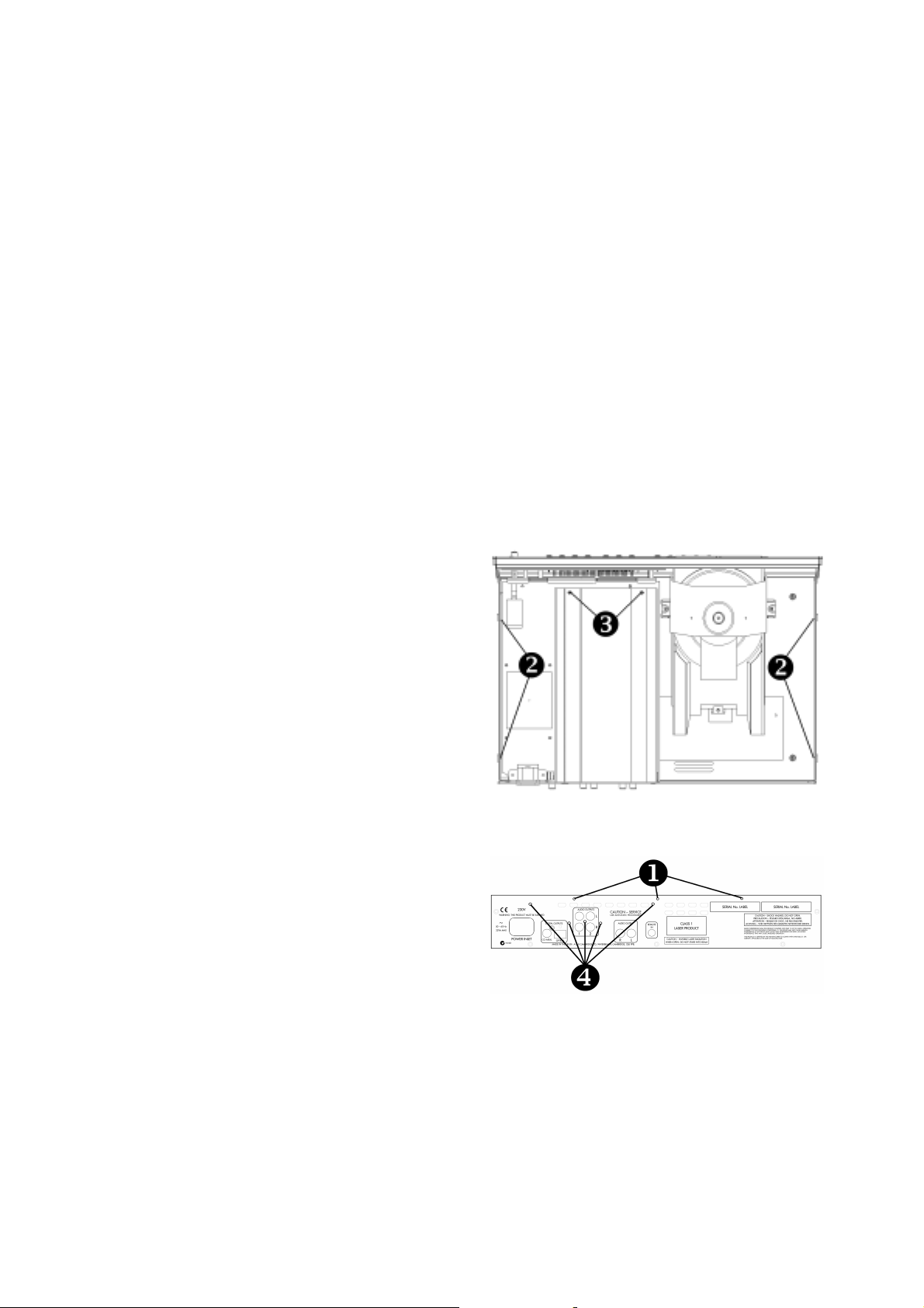
1. Disconnect the mains supply from the Alpha CD player.
2. Remove the top cover by taking out the 2 screws from the
top edge of the rear panel marked ! (Pozi no.1 driver
required and on each side marked " (Pozi no.2 driver
required).
3A. For Alpha 7/7SE to DiVA CD82 DAC upgrade only
Pull off the st i ck y pla st ic gask et b et ween t h e d i gita l ou tp ut
socket and the audio output sockets to reveal the 4 audio
output socket holes through which the DAC sockets will
pass.
Any remnants of adhesive can be removed by rubbing it
gently with your finger and rolling it off. We do not
recommend the use of solvents.
Fit the 2 supplied PCB (printed circuit board) pillars to the
holes in the main board on either side of the flex foil
coming from the display board, these are marked # in
figure 1. The big end of each PCB pillar goes into the
main PCB, these push in and clip home. Take great care
not to damage th e main circuit boa rd .
Remove the Alpha 7/7SE Configuration Module (the
small vertically mounted PCB in the centre of the main
board). It will not be needed once the new DAC board is
fitted.
Note: The original n ickel-plated audio outp ut sockets are
no longer connected after the upgrade and cannot be used.
However the digit al output still functions.
3B. For Alpha 8/8SE to DiVA CD82 DAC upgrade only
Remove the 5 screws holding the Alpha 8/8SE board in
place. Squ eeze the t op of the t wo PCB pi llars supp orting
the end of the aluminium extrusion and lift the extrusion
up and out of the unit. If the flex foils do not come away
with the DAC board then remove them as well.
4. Take static precautions first. With the aluminium
extrusion of th e CD82 DAC module uppermos t fit the
flex foils from the module into the appropriate sock ets
in the main board, ensuring they are pushed fully home.
You may find it helps to slide the module into the uni t
so that the audio output sockets fit through th e ho les in
the rear pan el and angle the module slightly upwa r ds to
achieve this.
5. Push the modu le down firmly on to the support pillars,
ensure it is latched in place.
6. Fit the supplied screws with integral washers to the 5
points marked $ in figure 1 (T10 Torq driver required)
to hold the module in place.
7. Refit the top cover and attach the CD82 authentication
label to the underside of the CD player
Upgrading a CD72 to CD82
1. Disconnect the mains supply from the DiVA CD player.
2. Remove the top cover by taking out the 3 screws from
the top edge of the rear panel ma r ked ! (T10 Torq
driver required) and on each side marked " (T20 Torq
driver required) in figure 1.
3. Pull off t he sticky plastic gasket between the digita l
output socket and the audio output sockets to reveal t he
4 audio output socket holes through which the DAC
board sockets will pass.
4. Any remnants of adhesive can be removed by rubbing it
gently with your finger and rolling it off. We do not
recommend the use of solvents.
5. Fit the 2 supplied PCB (printed circuit board) pillars to
the holes in the main board on either side of the flex foil
coming fro m the display bo ard, these are marked # in
figure 1. The big en d of each PCB pillar goes into the
main PCB, these push in and clip home. Take great
care not to da mage the main circuit board.
6. Remove the Configuration Module (the small vertically
mounted PCB in the centre of the main board). It will
not be needed once the new DAC board is fitted.
7. Note: The original ni ckel-plated audio output sock ets
are no longer connected after the upgrade and cannot be
used. However the digital output still fu nctions.
8. Remove the following jumpers: - PL2, PL3, PL4, PL6
Fit the following jumpers: - PL5, PL7
9. Take static precautions first. With the aluminium
extrusion of the CD82 DAC module uppermost fit the
flex foils from the module into the appropriate sock ets
in the main board, ensuring they are pushed fully home.
If they are not pushed fully home, the uni t may not read
discs. You may find it helps to slide the module into
the unit so that the audio output sockets fit thr ough the
holes in the r ear panel and angle the module slightly
upwards to ac hieve this.
10. Push the module down firmly on to the support pillars,
ensure it is latched in place.
11. Fit the supplied screws with integral washers to the 5
points marked $ in figure 1 (T10 Torq driver required)
to hold the module in place. Refit the top cover.
Page 6
12. Removing the drawer front - connect a mains supply to the
unit; press load and allow the tray to fully open; remove
the mains supp ly from the unit. Hold the drawer tightly
with one hand and with the other pu ll the drawer front
forward away from the player (pull hard). Remove any
remnants of tape from the drawer front mechanism; clean
the drawer mechanism front using the 'surface cleaner'
wipe provided.
13. Fitting the new CD82 drawer front - connect a mains
supply to the unit and allow the drawer to close
automatica lly. Remove the backing from the tap e attached
to the new drawer front and carefully align the drawer
front with the mechanism and press gently together;
reposition the drawer front if necessary and press firmly to
the unit.
Upgrading a CD72 (TEXT) to CD82 (TEXT)
1. Disconnect the mains supply from the DiVA CD player.
2. Remove the top cover by taking out the 3 screws from the
top edge of the rear panel marked ! (T10 Torq driver
required) and on each side marked " (T20 Torq driver
required) in figure 1.
3. Pull off th e sticky plastic gasket between the digital output
socket and the audio output sockets to reveal th e 4 audio
output socket holes through which the DAC board sockets
will pass.
4. Any remnants of adhesive can be removed by rubbing it
gently with your finger and rolling it off. We do not
recommend the use of solvents.
5. Fit the 2 supplied PCB (print ed circuit board) pillars to the
holes in the m ain board on either side of the flex foil
coming fro m the display bo ard, these are marked # in
figure 1. The big en d of each PCB pillar goes into the
main PCB, these push in and clip home. Take great care
not to damage th e main circuit boa rd .
6. Note: The original ni ckel-plated audio output sock ets are
no longer connected after the upgrade and cannot be used.
However the digital output still func tions.
7. Set the ma in board jumper settings as listed below: -
PL200 ON
PL201 ON
PL202 ON
PL203 OFF
PL204 ON
PL205 OFF
PL300 2 and 3
PL400 OFF
PL401 OFF
PL402 OFF
8. Take static precautions first. With the aluminium
extrusion of the DAC module uppermost fit the flex foils
from the module into the appropriate sockets in the main
board, ensuring they are pushed fully home. If they are
not pushed fully home, the unit may not read discs. You
may find it helps to slide the module into the unit so that
the audio outp ut sockets fit through the holes in the rear
panel and angle the module slightly upwards to achieve
this.
9. Push the modu le down firmly on to the support pillars,
ensure it is latched in place.
10. Fit the supplied screws with integral washers to the 5
points marked $ on figure 1 (T10 Torq driver required)
to secure the module in place. Refit the top cover.
11. Removing the drawer front - connect a mains supply to
the unit; press load and allow the tray to fully open;
remove the mains supply from the unit. Hold the drawer
tightly with one hand and with the other pull the drawer
front forward away from the player (pull hard). Remove
any remnants of tape from the drawer front mechanism;
clean the drawer mechanism front using th e 'surface
cleaner' wipe provided.
12. Fitting the new CD82 drawer front - connect a mains
supply to the unit and allow the drawer to close
automatica lly. Remove the backing from the tape
attached to the new drawer front and carefully align the
drawer front with the mechanism and press gently
together; reposition the drawer front if necessary and
press firmly to the unit.
Figure 1
Page 7

Main
Board
L934
Contents
!
Circuit description
!
Component overlay
!
Parts list
!
Circuit diagrams
Page 8

CD72, CD82 & CD92 (text)
Circuit Description
Summary
The main Motherboard/Display PCBs for the Diva CD players
may be assembled as three different versions:
! DiVA CD62 (text) - With alternate components fitted
and the 92DAC upgrade connections omitted
(L933AY).
! DiVA CD72 (text) - With the standard set of
components fitted (L899AY).
! DiVA CD82/92 (text) - With analogue components
and connectors omitted, for use as a host motherboard
The CD72T version may be converted for use with an upgrade
All system s are based on a Sony kit, comprising CDM14BL5BD25 CD transport / loader / laser mechanism, micro-controller
and fluorescent display.
Power Supplies
The CD72, CD82 & CD92 transformers :-
The mains transformer has three secondary windings:
1. 13.7V – 0V – 13.7V to provide ±12V(A) supplies
2. 9V-0V-32V to produce the digital, motor drive and
All of these supplies are delivered also to the optional CD82 or
CD92DAC upgrade board via the DAC power connector SK203.
The supplies are conventional and are linearly regulated by 3terminal voltage regulators.
When the DAC upgrade board is used, analogue regulators IC201
and IC205 can be bypassed by rem oving JP203 and JP205, and
fitting JP202 and JP204
DAC board itself. Soft-charging resistors R204 and R205 are
bypassed similarly.
Relay Mute Control
This circuit drives a relay to un-mute the analogue output ~5
seconds after the unit is powered on, and quickly mutes the
output when the unit is switched off. Th e cir cu it works
effectively as an “AND” gate.
for the plug-in 82 or 92DAC (L934AY).
plug-in DAC board by changing on-board jumpers.
! 230/115VAC - part number L866TX
! 100VAC only - part number L851TX
(IC201 and IC205) for the audio output circuitry via
regulators IC201 and IC205.
fluorescent display grid supplies:
+11V(U) Unregulated supply for relay drive and
+7V (IC200) Mechanism and motor driver
+5V(D) (IC202) General digital logic supply
+5V(A) (IC203) Supply to DAC
-30V (IC204) Display grid voltage.
3. 0-5V to provide an AC supply for the display
filament.
+5V(D) supply
supply
since regulation is contained on the
If AC is present on the transformer secondary winding and the 5second timer composed of R222 and C221 has reached the
threshold voltage (Vbe of TR200 + Vbe of TR201 - Vce of
TR202, or ~1.0V), the relay coil is connected to +11V
(referenced to 0V_3 as required by the DAC’s internal circuitry)
via TR204.
When AC is removed, C231 discharges quickly through R225,
the base voltage of TR204 rises and the relay coil voltage is
removed, muting t he output.
TR203 resets the ‘timer’ by discharging C221 quickly at turn-off.
Remote Control/PIC Micro
Remote control data is received from the IREy e on the display PCB
and buffered by TR300 and TR301. The Programmable Interrupt
Controller converts the RC-5 format data into the NEC format
required by the Sony micro. The PIC al so control s the con fig ura tio n
of the digital filter/DAC on the DAC board.
Motor Driver
The status of the drawer is indicated to the micro by two micro
switches ‘INSW’ and ‘OUTSW’ on SK205. The micro controls
the drawer motor via driver IC303.
Clock Buffering
The clock and data signals LRCK, ADATA and BCLK from the
mechanism connector SK300 are double buffered by IC300
before being delivered to the D AC.
Power-On/Reset
The power-on reset signal XRST (or RESET) is generated by
R409, C410 and IC404. When the power is turned on, C410 is
initially uncharged and pin 11 of IC404 is at high voltage, and
thus the output is low. After a short time, C410 is charged via
R409; IC404 pin 11 is then low, and the output switches high
(RESET is de-asserted).
DAC & System Clock
The DAC is a Burr Brown PCM1716E, the DAC is configured
for hardware control.
Digital audio is input on pins 1, 2 & 3 in standard Red Book
Audio format, i.e. Word Cloc k, Bit Clock an d Data.
The system clock is based around 16. 9344 MH Z crystal X400
and transistor TR402. This produces a stable clock with low
jitter. IC404A & B buffer the clock as linear buffers. IC404C &
D buffer the individual mech & DAC clock lines.
The CD82 & CD92 system clock is generated on the DAC board.
The clock and data signals LRCK, ADATA and BCLK from the
mechanism connector SK300 are double buffered by IC300 before
being delivered to the DAC. The system clock is delivered to the
mech via two-position jumper PL300. The clo ck source is selected
to be either from the main board (CD62/72) or from the DA C bo ar d
(CD82/CD92) by the position of JP300.
When the 82 or 92DAC is fitted as an upgrade to a CD72, r emov ing
JP400 disables the main board clock
Page 9

Analogue Output
Left channel:
IC400A and IC400B are cascaded 69kHz 2
Bessel filters. The output devices internal to both op-amps in
IC400 are “pulled down” to the negative supply rail to force
operation in class A (one output device is conducting at all times
and crossover distortion is eliminated).
IC402A is a DC servo with a very low cut off frequency, acting
to impose a non-zero voltage ‘virtual earth’ at the non-inverting
input of IC400B, thus eliminating the offsets caused by the pulldown resistors and DC-coupling the output.
The right channel is the same as the left channel. IC401A & B
are used as the buffer and filter.
nd
order low-pass
Microcontroller & Display Board
The system microcontroller IC100 serves the following functions:
! Control of the mechanism & decoder on the CDM14
mechanism
! Control of mute, attenuation and de-emphasis for the
DAC
! Direct drive of the fluorescent display
! Remote control decoding
! Keyboard scanning
! 82/92DAC muting
The keyboard scanning works by connecting the keys to a resistor
ladder on an ADC input to the micro. Pressing a key presents a
unique voltage to this input, which the micro is pre-programmed
to interpret accordingly.
The remote control data contains a ‘Customer Code’ that
identifies this as an Arcam product. The diode network D100 to
D106 configures the micro to accept this code.
Remote Bus Carrier Filter & Demodulator
Remote control commands can be delivered over wire to SK500
for multi-room applications. Incoming signals are attenuated and
clipped by resistors and D500. L500 and C508 form a parallel
resonant circuit at approximately 37kHz. This dem odulates the
incoming signal and the output is passed to IC501A where it is
‘chopped’, low pass filtered and fed to IC501B to provide the
RC5 outp ut signal.
Digital Output
The decoder on the mechanism assembly generates an SPDIF
format digital output signal. This is passed to buffer IC500A.
IC500B through E are used in parallel to provide a transformer
less 75-ohm source impedance to a single phono socket SK501.
Optical digital output via IC502 is also tapped off the digital
output signal via IC500F.
Page 10
Page 11

L934 Main Board Parts List Issue 4.1
Designator Part Description
BR200 3BDF01M Bridge rectifier DF01M 1A 100V
BR201 3BDF01M Bridge rectifier DF01M 1A 100V
C100 2A210 CERD 1N0 63V 20% RA
C101 2A210 CERD 1N0 63V 20% RA
C102 2A210 CERD 1N0 63V 20% RA
C103 2N710 ELST 100U 25V
C104 2A410 CERD 100N 63V 20% RA
C105 2A410 CERD 100N 63V 20% RA
C106 2A410 CERD 100N 63V 20% RA
C107 2A410 CERD 100N 63V 20% RA
C108 2A410 CERD 100N 63V 20% RA
C109 2A410 CERD 100N 63V 20% RA
C110 2N610 ELST 10U 50V
C129 2A310 CERD 10N 63V 20% RA
C151 2A210 CERD 1N0 63V 20% RA
C152 2A210 CERD 1N0 63V 20% RA
C153 2A210 CERD 1N0 63V 20% RA
C154 2A210 CERD 1N0 63V 20% RA
C155 2A210 CERD 1N0 63V 20% RA
C156 2A210 CERD 1N0 63V 20% RA
C200 2K233 SUPPR CAP 3N3 250V
C201 2K233 SUPPR CAP 3N3 250V
C202 2K233 SUPPR CAP 3N3 250V
C203 2D422 220NF CLASS X2 CAP 275VRMS
C204 2A410 CERD 100N 63V 20% RA
C205 2A410 CERD 100N 63V 20% RA
C206 2A410 CERD 100N 63V 20% RA
C207 2AB410 CERD 100N 100V -20% +80% RA
C208 2AB410 CERD 100N 100V -20% +80% RA
C209 2A410 CERD 100N 63V 20% RA
C210 2N833 ELST 3M3 25V
C211 2N810C ELST 1M0 35V
C212 2N810C ELST 1M0 35V
C215 2K410 PEST 100N 63V 10%
C218 2N710 ELST 100U 25V
C219 2N710 ELST 100U 25V
C220 2N710 ELST 100U 25V
C221 2N710 ELST 100U 25V
C222 2N710 ELST 100U 25V
C223 2N810 ELST 1M0 25V
C224 2N810 ELST 1M0 25V
C225 2N710B ELST 100U 100V
C226 2N710B ELST 100U 100V
C227 2N710B ELST 100U 100V
C228 2N810A ELST 1M0 10V
C229 2N810A ELST 1M0 10V
C230 2N710 ELST 100U 25V
C231 2N610 ELST 10U 50V
C300 2A410 CERD 100N 63V 20% RA
C301 2A410 CERD 100N 63V 20% RA
C302 2A410 CERD 100N 63V 20% RA
C303 2A410 CERD 100N 63V 20% RA
C304 2A110 CERD 100P 50V -20% +80% RA
C305 2N710 ELST 100U 25V
C306 2N710 ELST 100U 25V
C307 2A310 CERD 10N 63V 20% RA
C308 2A410 CERD 100N 63V 20% RA
C400 2A410 CERD 100N 63V 20% RA
C410 2N710 ELST 100U 25V
C414 2A410 CERD 100N 63V 20% RA
C434 2A410 CERD 100N 63V 20% RA
C451 2AA210 CAP 1000PF 100V NPO CERD
Page 12

L934 Main Board Parts List Issue 4.1
Designator Part Description
C452 2AA210 CAP 1000PF 100V NPO CERD
C500 2A410 CERD 100N 63V 20% RA
C501 2A310 CERD 10N 63V 20% RA
C502 2K447 PEST 470N 63V 10%
C503 2A210 CERD 1N0 63V 20% RA
C504 2A310 CERD 10N 63V 20% RA
C505 2A410 CERD 100N 63V 20% RA
C506 2P622 ELST 22U 20V OSCON
C507 2A410 CERD 100N 63V 20% RA
C508 2D168 PPRO 680P 5% 63V RA
C509 2A410 CERD 100N 63V 20% RA
C510 2A110 CERD 100P 50V -20% +80% RA
C511 2A410 CERD 100N 63V 20% RA
C512 2A147 CERD 470P 50V -20% +80% RA
C513 2A110 CERD 100P 50V -20% +80% RA
CA1 L920CA CD...T MAINS JUMPER CABLE
D100 3A4148 SSDIODE 1N4148 75V
D101 3A4148 SSDIODE 1N4148 75V
D102 3A4148 SSDIODE 1N4148 75V
D103 3A4148 SSDIODE 1N4148 75V
D104 3A4148 SSDIODE 1N4148 75V
D105 3A4148 SSDIODE 1N4148 75V
D106 3A4148 SSDIODE 1N4148 75V
D200 3A4148 SSDIODE 1N4148 75V
D201 3A4148 SSDIODE 1N4148 75V
D205 3A4148 SSDIODE 1N4148 75V
D206 3A4148 SSDIODE 1N4148 75V
D208 3A4148 SSDIODE 1N4148 75V
D209 3A4148 SSDIODE 1N4148 75V
D210 3A4148 SSDIODE 1N4148 75V
D211 3A4148 SSDIODE 1N4148 75V
D212 3A4148 SSDIODE 1N4148 75V
D213 3B4003 RECTIFIER 1N4003F 1A 200V
D214 3C05104 Diode 5V1 400mW
D215 3A4148 SSDIODE 1N4148 75V
D300 3A4148 SSDIODE 1N4148 75V
D301 3C04704 ZENER 4V7 400MW
D400 3A4148 SSDIODE 1N4148 75V
D500 3C04704 ZENER 4V7 400MW
DISP100 B1015 DISP CD SONY 14-ST-20GK
E1 E102AY CDTEXT VFD SUPPORT
EL200 8M101 EARTH LEAD
FS200 F022 INS COVER PCB FUSEHOLDER
FS200 8S004 FUSEHOLDER 20mm PCB
FS201 C11166 FUSE 20mm 160mA T S504160mA
FS201 F022 INS COVER PCB FUSEHOLDER
FS201 8S004 FUSEHOLDER 20mm PCB
HS200 F006 HEATSINK CLIP TO220 13/8.6 DC/W
HS200 F008 HEATSINK TO220 8.6 DEGC/W
HS201 F007 HEATSINK TO220 CLIP 30
HS202 F007 HEATSINK TO220 CLIP 30
IC100 5G82832 IC CD CXP82832-031Q MICRO
IC200 5D1086A IC VREG LM1086CT-ADJ
IC202 5D317T IC VREG POS LM317T
IC203 5D317T IC VREG POS LM317T
IC204 5D337 IC VREG POS LM337T
IC300 5J7404 IC HCMOS 74HCU04
IC302 5H16C54X IC CMOS MICRO PIC16C54XT/P
IC302 8S018 IC SOCKET 18 PIN 0.3''
IC302SW L825SW A SOFTWARE
IC303 5Q1641 IC MOTOR DRIVER LB1641
IC404 5J7404 IC HCMOS 74HCU04
Page 13

L934 Main Board Parts List Issue 4.1
Designator Part Description
IC500 5J7404 IC HCMOS 74HCU04
IC501 5M393A IC COMPARITOR DUAL LM393A
IC502 5TG550T SPDIF OPTICAL TRANSMITTER
JP200 8K004 JUMPER SOCKET 0.1''
JP201 8K004 JUMPER SOCKET 0.1''
JP202 8K004 JUMPER SOCKET 0.1''
JP204 8K004 JUMPER SOCKET 0.1''
JP300 8K004 JUMPER SOCKET 0.1''
L200 7D968A 6U8H INDUCTOR
L201 7D968A 6U8H INDUCTOR
L400 7F003 FERRITE BEAD SINGLE AXIAL
L500 7D327 27mH INDUCTOR
L501 7F003 FERRITE BEAD SINGLE AXIAL
LED100 3D007 LED GREEN 3.1MM SLR-37MG3F
LED101 3D003 LED ULTRARED 5MM
LK600 1H000 RES MF W4 1% 0R0
LK601 1H000 RES MF W4 1% 0R0
MC200 E922MC MAGNETIC SHIELD PLATE
MC201 E923MC ADHESIVE PAD(ATTACH TO E922MC & TX)
PAD100 E802AP SORBOTHANE PAD 15X6X3 mm
PAD101 E802AP SORBOTHANE PAD 15X6X3 mm
PB L899PB_4 BLANK PCB
PL200 8K6201 2WAY MOLEX VERT MALE CONNECTOR
PL201 8K6201 2WAY MOLEX VERT MALE CONNECTOR
PL202 8K6201 2WAY MOLEX VERT MALE CONNECTOR
PL204 8K6201 2WAY MOLEX VERT MALE CONNECTOR
PL300 8K2103 3WAY MOLEX VERT MALE CONNECTOR
R100 1H122 RES MF W4 1% 220R
R101 1H310 RES MF W4 1% 10K
R102 1H310 RES MF W4 1% 10K
R103 1H268 RES MF W4 1% 6K8
R104 1H268 RES MF W4 1% 6K8
R105 1H268 RES MF W4 1% 6K8
R106 1H268 RES MF W4 1% 6K8
R107 1H268 RES MF W4 1% 6K8
R108 1H233 RES MF W4 1% 3K3
R109 1H222 RES MF W4 1% 2K2
R110 1H215 RES MF W4 1% 1K5
R111 1H210 RES MF W4 1% 1K0
R112 1H168 RES MF W4 1% 680R
R113 1H010 RES MF W4 1% 10R
R114 1H310 RES MF W4 1% 10K
R115 1H310 RES MF W4 1% 10K
R116 1H310 RES MF W4 1% 10K
R117 1H310 RES MF W4 1% 10K
R200 1G810 RES MF FU W3 1R0 5% NFR25
R201 1G810 RES MF FU W3 1R0 5% NFR25
R202 1K515 RES W25 5% VR25 1M5
R203 1H133 RES MF W4 1% 330R
R210 1G810 RES MF FU W3 1R0 5% NFR25
R211 1G010 RES MF FU W3 10R 5% NFR25
R212 1G810 RES MF FU W3 1R0 5% NFR25
R213 1G010 RES MF FU W3 10R 5% NFR25
R214 1H216 RES MF W4 1% 1K6
R215 1H322 RES MF W4 1% 22K
R216 1H210 RES MF W4 1% 1K0
R217 1H333 RES MF W4 1% 33K
R218 1H127 RES MF W4 1% 270R
R219 1H127 RES MF W4 1% 270R
R220 1H182 RES MF W4 1% 820R
R221 1H182 RES MF W4 1% 820R
R222 1H447 RES MF W4 1% 470K
Page 14

L934 Main Board Parts List Issue 4.1
Designator Part Description
R223 1H310 RES MF W4 1% 10K
R224 1H310 RES MF W4 1% 10K
R225 1H222 RES MF W4 1% 2K2
R226 1H310 RES MF W4 1% 10K
R227 1H110 RES MF W4 1% 100R
R228 1H110 RES MF W4 1% 100R
R229 1H215 RES MF W4 1% 1K5
R230 1H310 RES MF W4 1% 10K
R300 1H133 RES MF W4 1% 330R
R303 1H268 RES MF W4 1% 6K8
R304 1H133 RES MF W4 1% 330R
R306 1H133 RES MF W4 1% 330R
R307 1H310 RES MF W4 1% 10K
R308 1H310 RES MF W4 1% 10K
R309 1H310 RES MF W4 1% 10K
R310 1H310 RES MF W4 1% 10K
R311 1H410 RES MF W4 1% 100K
R312 1H268 RES MF W4 1% 6K8
R313 1H410 RES MF W4 1% 100K
R314 1H310 RES MF W4 1% 10K
R315 1H310 RES MF W4 1% 10K
R409 1H310 RES MF W4 1% 10K
R432 1H310 RES MF W4 1% 10K
R439 1H510 RES MF W4 1% 1M0
R500 1H010 RES MF W4 1% 10R
R501 1H010 RES MF W4 1% 10R
R502 1H218 RES MF W4 1% 1K8
R503 1H218 RES MF W4 1% 1K8
R504 1H210 RES MF W4 1% 1K0
R505 1H112 RES MF W4 1% 120R
R506 1H212 RES MF W4 1% 1K2
R507 1H310 RES MF W4 1% 10K
R508 1H310 RES MF W4 1% 10K
R509 1H310 RES MF W4 1% 10K
R510 1H310 RES MF W4 1% 10K
R511 1H147 RES MF W4 1% 470R
R512 1H410 RES MF W4 1% 100K
R513 1H410 RES MF W4 1% 100K
R514 1H215 RES MF W4 1% 1K5
R515 1H310 RES MF W4 1% 10K
R516 1H212 RES MF W4 1% 1K2
R517 1H212 RES MF W4 1% 1K2
R518 1H212 RES MF W4 1% 1K2
R519 1H110 RES MF W4 1% 100R
RX100 B2107 REMOTE RX PIC-26043TM2 38KHZ
SH400 E821MC PHONO EMC SHIELD
SK100 8K8132 32-WAY FFC CONN HORIZ
SK200 8A001 IEC MAINS CONN PCB INS PX
SK200 HP007 COPPER RIVET TCP/D48 BS
SK200 HP007 COPPER RIVET TCP/D48 BS
SK203 8K8023 23-WAY FFC CONN VERT
SK300 8K8023 23-WAY FFC CONN VERT
SK301 8K8032 32-WAY FFC CONN VERT
SK302 8K8032 32-WAY FFC CONN VERT
SK303 8K2005 5-WAY AMP CT CONN
SK500 8D228 MIN JACK SINGLE 3.5mm
SK501 8D220 PHONO SKT SINGLE EMC
SP102 F195 LED SPACER
SP103 F205 DS STICKY PAD 70 X 12mm
SP104 E822AP IR RX SUPPORT PAD
SW100 A1511 TACT SWITCH 2-PIN LOW PROF 9.5mm
SW101 A1511 TACT SWITCH 2-PIN LOW PROF 9.5mm
Page 15

L934 Main Board Parts List Issue 4.1
Designator Part Description
SW102 A1511 TACT SWITCH 2-PIN LOW PROF 9.5mm
SW103 A1511 TACT SWITCH 2-PIN LOW PROF 9.5mm
SW104 A1511 TACT SWITCH 2-PIN LOW PROF 9.5mm
SW105 A1511 TACT SWITCH 2-PIN LOW PROF 9.5mm
SW106 A1511 TACT SWITCH 2-PIN LOW PROF 9.5mm
SW107 A1511 TACT SWITCH 2-PIN LOW PROF 9.5mm
SW200 A1010 SWITCH PUSH MAINS DPST TV-8
TR200 4A549 TRANS LF SS N BC549B
TR201 4A549 TRANS LF SS N BC549B
TR202 4A549 TRANS LF SS N BC549B
TR203 4A549 TRANS LF SS N BC549B
TR204 4A557 TRANS LF SS P BC557B
TR300 4A549 TRANS LF SS N BC549B
TR301 4A549 TRANS LF SS N BC549B
TX200 L866TX 9 CD COOL FRAME TX MULTI-VOLTAGE
X100 7W008 CER RESON 8.00MHz
X300 7W005 CER RESON 4.00MHz
Y200 F185 TX WIRE RESTRAINT
Page 16

87654321
(NEAR SK100)
CHASSIS
D
C
B
FIX100
FIXING HOLE 3.2
FIX101
FIXING HOLE 3.2
C101
1N0 CD
0V
FIX102
FIXING HOLE 3.5
FIX103
FIXING HOLE 3.5
CHASSIS2
C100
1N0 CD
C102
1N0 CD
0V 0V
PAD100
SORBOTHANE PAD
15 X 6 X 3 mm
SORBO E802AP
PLACED BETWEEN C409 AND L401
PAD101
SORBOTHANE
HALF PAD
7.5 X 6 X 3 mm
SORBO HALF PAD E802AP
FITTED ON X400
SP102
LED
SPACER
SPACER F195
SP103
70mm x 12mm
DOUBLE SIDED
STICKY GASKET
70X12_DS STICKY TAPE
SP104
IR RX
SUPPORT PAD
IR RX SUPPORT PAD
+5V
(NEAR SK100)
0V
RX100
SBX1610-52/PIC-26043TM2
Connector to main PCB
PIN 1 TO LEFT
CABLE POINTING DOWN
IR_DISP
SK100
FFC32H
2
32
31
30
29
28
27
26
25
24
23
22
21
20
19
18
17
16
15
14
13
12
11
10
9
8
7
6
5
4
3
2
1
+
C103
100U EL
3
O/P
+5V
O/P
Case
Case
F1
SCOR_DISP
RMIN_DISP
LDOUT_DISP
LDIN_DISP
SENS_DISP
XLT_DISP
AMUTE_DISP
CLK_DISP
LDON_DISP
DATA_DISP
SQCK_DISP
SUBQ_DISP
LOADSW_DISP
XRST_DISP
DEEM_DISP
HDCD_DISP
LPH_DISP
F2
IR_DISP
DECOUPLING CAPACITORS FOR IC100
C104
100N CD
C107
100N CD
C105
100N CD
-30V
+5V
GND +5V
C108
100N CD
GND
+
C110
10U EL
1
+5V
0V
-30V
SW100 SW101 SW102 SW103 SW104 SW105 SW106 SW107
0V
R113
10R MF
0V
NEXT PREV FF FR PAUSE STOP PLAY OPEN
C106
100N CD
HDCD LED
LED101
LED ULTRARED
0V
R101
10K MF
R100
220R MF
LED100
LED GREEN3.1MM
POWER LED
R103
6K8 MF
R108
3K3 MF
CMO4
R109
2K2 MF
D100
1N4148
D101
1N4148
REMOTE CUSTOM CODE DIODE MATRIX
D102
1N4148
D103
1N4148
D104
1N4148
D106
1N4148
CMO3
CMO2
CMO1
0V
C109
100N CD
0V
R110
1K5 MF
R111
1K0 MF
R112
680R MF
D105
1N4148
R114
R115
R116
R117
+5V
10K MF
10K MF
10K MF
10K MF
R104
6K8 MF
C129
10N CD
0V
R105
6K8 MF
R106
6K8 MF
R107
6K8 MF
R102
10K MF
10
11
12
13
14
15
16
17
18
19
20
21
22
23
24
25
26
27
28
29
30
1
2
3
4
5
6
7
8
9
13G
14G
NC
CMI1
SCOR
CMI2
CMI3
RMIN
CMI4
NC
NC
LDOUT
LDIN
SENS
XLT
AMUTE
PGML
NC
NC
TIMER
NC
CLK
LDON
DATA
SQCK
SUBQ
NC
AVREF
KEY0
KEY1
DISP100
DISPLAY 14-ST-20GK
F11F1214G413G512G611G710G89G98G107G116G125G134G143G152G161G17NC18P119P220P321P422P523P624P725P826P927P1028P1129P1230P1331P1432P1533P1634P1735P1836P1937P2038P2139F241F2
+5V
871G88
100
10G9811G9912G
KEY231KEY332ADJ/AFADJ
LOADSW34NC35NC36AVSS37RST38EXTAL39XTAL40VSS41NC42NC43VDD44VDP45NC
33
892G903G914G925G936G947G958G969G97
VDD
-30V
+5V
0V
X100
CST8.00
S385S286S1
S484S583S682S7
NC47LPH48NC49NC
46
81
S10
S11
S12
S13
S14
S15
S16
S17
S18
S19
S20
S21
NC
NC
NC
NC
NC
NC
NC
NC
EMPHASIS
CMO4
CMO3
CMO2
CMO1
NC
NC
NC
50
S8
S9
80
79
78
77
76
75
74
73
72
71
70
69
68
67
66
65
64
63
62
61
60
59
58
57
56
55
54
53
52
51
IC100
CXP82832
CMO4
CMO3
CMO2
CMO1
0V
D
42
F2F1
C
B
E1
CDTXT VFD SUPP INSULATED
A
E102AY
1
2
3
4
0V
1 2 3 4 5 6 7 8
A & R Cambridge Ltd.
Pembroke Avenue
Denny Industrial Centre
Waterbeach
Cambridge CB5 9PB
Filename
J:\Change_Control\ECO_AGENDA\01_E007_Display_Cradle_see_tgp\L934_4.1.DDB - Documents\L934C1_4.1.sch
23425
DRAWING TITLE
CD92T - DISPLAY AND SYSTEM MICRO
Circuit Diagram
Notes:
01_E007 4.1WAF/TGP 13/12/01
01_1123 TGP
CW 1.0
ECO No. DESCRIPTION OF CHANGE
INITIALS
DATE
Date Printed
DISPLAY CRADLE CHANGED TO INSULATED ASSY
UPDATE FOR EMC AND WILSONS REQUESTS01_1147 4.0WAF 24/10/01 & UPDATE PCB TO AIWA STD
Up-Issue for PCB 2.1
Initial Release
Drawn by:
JR14-Dec-2001
1 7Sheet of
DRAWING NO.
A
ISSUE
L934CT
Page 17

SK200
IEC3
EL200
N E L
L
E
N
C200
C201
3N3(X1Y2)
3N3(X1Y2)
R202
NEUTRAL LIVE
NEUTRAL2
SK202
3
2
1
MOLEXPWR6
(FOR AUX TOROID)
NF
L200
6U8H
1M5 VR25
C203
220N(X2)
CA1
L920CA
L920CA
6
5
4
L201
6U8H
BRN BRN
BLU
BLU
EARTH LEAD
8M101
EARTH LEAD
(IEC INLET TO CHASSIS)
LIVE2
C202
3N3(X1Y2)
FS200
T250MA115V
115V ONLY
FS201
T160MA
230V ONLY
NEUTRAL2
SW200A
A1010
SW200B
A1010
115V
230V
115V
10
230V
1
2
7
6
4
5
9
TX200
L866TX
16
TX_16
17
18
TX_18
11
13
15
AC_3
19
TX_19
R210
20
TX_20
NB: CABLE ASSEMBLY L920CA GOES BETWEEN
BRN BRN AND BLU BLU FROM MAINS SWITCH TO BACK OF PCB
FILA
FILB
Y200
TX WIRE CLIP
TX FIXING SCREWS
Y201
SCREW HF4V09B
Y203
SCREW HF4V09B
Y202
SCREW HF4V09B
Y204
SCREW HF4V09B
AC1
AC2
D209
1N4148
D210
1N4148
R213
10R FU
R200
1R0 FU
R201
1R0 FU
AC1
C206
100N CD
AC2
C207
100N CD 100V
R211
10R FU
1R0 FU
R212
1R0 FU
C230
100U EL
100N CD 100V
+
C204
100N CD
C205
100N CD
C208
R224
10K MF
SK201
MOLEXPWR4
(FOR AUX TOROID)
1
3
+11V(U)
BR200
DF01M +
D213
1N4003
R227
100R MF
R228
100R MF
R222
470K MF
C221
+
100U EL
0V_3
+
C231
10U EL
2
4
C210
3M3 EL
+
C225
100U EL 100V
R223
10K MF
R225
2K2 MF
NF
IC200
LM1086-ADJ
I
Vin
I
Vin
IC204
TR200
BC549B
D200
1N4148
HS201
TO220HS30REG
O
Vout
ADJ
R203
330R MF
A
+
C218
100U EL
+
C226
100U EL 100V
A
ADJ
LM337T
Vout
R214
1K6 MF
R215
22K MF
R216
1K0 MF
O
D205
1N4148
Relay control for AC detect
R226
10K MF
R229
1K5 MF
TR201
BC549B
TR202
BC549B TR203
TR204
BC557B
R230
10K MF
D201
1N4148
-30VF
+
+7V
+
C227
100U EL 100V
Filiament supply
BC549B
Motor drive supply
C228
1M0 10V
D215
1N4148
R217
33K MF
D214
5V1 400MW
+12V(A)
-12V(A)
+5V(A)
+5V(D)
RLYPWR
+11V(U)
BR201
DF01M
0V_2
PL200
2WVERTJUMPER
1
2
R204
NF
10R MF
R205
NF
10R MF
1
2
PL201
2WVERTJUMPER
SK203
23
22
21
20
19
18
17
16
15
14
13
12
11
10
9
8
7
6
5
4
3
2
1
FFC23V
Power connector for 9DAC PCB
0V_9DAC
JP200
JUMPER
JP201
JUMPER
+
C211
1M0 35V
+
C212
1M0 35V
Analogue op-amp supplies
IC201
I
Vin
C213
NF
100N PE
C214
NF
100N PE
I
Vin
+11V(U)
IC202
I
Vin
HS
C209
100N CD
IC203
I
Vin
C215
100N PE
NF
LM317T
A
A
LM337T
D206
1N4148
LM317T
A
D211
1N4148
LM317T
A
ADJ
+
C216
100U EL
+
C217
100U EL
IC205
ADJ
ADJ
+
C219
100U EL
ADJ
+
C222
100U EL
D202
1N4148
Vout
NF
Vout
D207
1N4148
Vout
Vout
NF
O
NF
NF
O
NF
O
O
PL202
2WVERTJUMPER
1
2
JP202
JUMPER
R206
NF
220R MF
R208
NF
1K8 MF
R209
NF
1K8 MF
R207
NF
220R MF
JP204
JUMPER
1
2
PL204
2WVERTJUMPER
HS200
TO220HS08REG
R218
270R MF
R220
820R MF
HS202
TO220HS30REG
R219
270R MF
R221
820R MF
D203
1N4148
D204
1N4148
D208
1N4148
D212
1N4148
2
JP203
JUMPER
NF
NF
JP205
JUMPER
1
+12V(A)
PL203
2WVERTJUMPER
1
NF
+
+
NF
2
2WVERTJUMPER
PL205
-12V(A)
+5V(D)
+
0V_2
+5V(A)
+
0V_1
NF
C223
1M0 25V
0V_1
C224
1M0 25V
NF
Digital +5V
C220
100U EL
DAC supply
C229
1M0 10V
AFFIX TO TX BETWEEN ANALOGUE CIRCUITRY & TX
MC200
E922MC
E922MC
MC201
E923MC
E923MC
0V_3
DRAWING TITLE
CD92T - POWER SUPPLIES
23425
A & R Cambridge Ltd.
Pembroke Avenue
Denny Industrial Centre
Waterbeach
Cambridge CB5 9PB
Notes:
Filename
J:\Change_Control\ECO_AGENDA\01_E007_Display_Cradle_see_tgp\L934_4.1.DDB - Documents\L934C2_4.1.sch
0V_3
Circuit Diagram
01_E007 4.1WAF/TGP 13/12/01 DISPLAY CRADLE CHANGED TO INSULATED ASSY
UPDATE FOR EMC AND WILSONS REQUESTS01_1147 4.0WAF 24/10/01 & UPDATE PCB TO AIWA STD
01_1123
ECO No. DESCRIPTION OF CHANGE
Date Printed
TGP Up-Issue for PCB 2.1
CW
INITIALS
DATE
Drawn by:
JR14-Dec-2001
L920CA ADDED TO SCM 1.0
2 7Sheet of
DRAWING NO.
ISSUE
L934CT
Page 18

87654321
Data connector to DAC PCB
SK301
FFC32V
+5V(D)
+5V(D)
0V_DIG
R301
330R MF
R300
330R MF
R302
330R MF
NF
R304
330R MF
R305
330R MF
NF
R306
330R MF
RA0
AMUTE
DEEM
RMIN
XRST
RESET
BCLK
ADATA
LRCK
R311
100K MF
+5V(D)
R313
100K MF
14
D
DIGOP
C
B
C300
100N CD
0V_DIG
Flex connector from CDM14BL-5BD25 mech
+5V(D)
0V_DIG
+7V
0V_DIG
IREYE
IC300G
74HCU04 NF
7
SK300
FFC23V
23
22
21
20
19
18
17
16
15
14
13
12
11
10
9
8
7
6
5
4
3
2
1
R314
10K MF
CLK
XRST
DATA
LDON
SENS
XLT
SUBQ
SQCK
AMUTE
BCLK
SCOR
ADATA
LRCK
LPH
0V_DIG
R307
10K MF
RC5 IP
C301
100N CD
BCLK
ADATA
LRCK
PL300
3WVERTJUMPER
1
2
JP300
3
JUMPER
(Master clock select jumper)
R308
10K MF
TR300
BC549B
R310
10K MF
IC300A
1 2
74HCU04
IC300C
5 6
74HCU04
IC300E
74HCU04
17MHZ
+5V(D)
1011
(From crystal oscillator)
(From 9 DAC PCB)
R309
10K MF
TR301
BC549B
3 4
IC300B
74HCU04
IC300D
74HCU04
IC300F
74HCU04
C304
100P CD
89
1213
D300
1N4148
30
31
32
27
28
29
IC302
PIC16C54XT
17
RA0
18
RA1
1
RA2
2
RA3
3
RTCC
4
MCLR
16
25
26
OSC1
X300
CST4.00
0V_DIG
20
21
22
23
24
XRST
AMUTE
VSS
OSC2
5
15
19
RB0
RB1
RB2
RB3
RB4
RB5
RB6
RB7
18
14
16
17
DEEM
6
7
8
9
10
11
12
13
VDD
C302
100N CD
15
RA0
13
14
RB6
+5V(D)
+
11
12
RB5
RB4
RB0
RB4
RB5
RB6
C305
100U EL
10
RB0
123456789
0V_9DAC
HDCD
Flexfoil connector to Display PCB
SK302
FFC32V
+5V(D)
Motor Drive
IC303
LB1641
O/P 'Out'
Vcc
Vcc
LoadOut
LoadIn
Bias
O/P 'In'
GND
32
31
0V_DIG
FILA
10
9
8
7
6
5
4
3
2
1
28
29
30
SCOR
LDOUT
LDIN
D301
4V7 400MW
27
25
26
RMIN
LDOUT
C303
100N CD
24
LDIN
22
23
SENS
+7V
0V_MOT
21
XLT
+
19
20
AMUTE
C306
100U EL
HDCD
DEEM
LPH
R303
6K8 MF
LOADSW
R312
6K8 MF
123456789
IREYE
FILB
R315
10K MF
0V_DIG
SK303
8K2005
1
2
3
4
5
EMPHASIS
LOADOUT
LOADIN
GND
INSW
OUTSW
D
C
B
10
11
12
13
14
15
16
17
18
CLK
LDON
DATA
SQCK
SUBQ
LOADSW
XRST
-30VF
+5V(D)
C307
10N CD
C308
100N CD
0V_MOT
0V_DIG
A
A & R Cambridge Ltd.
Pembroke Avenue
Denny Industrial Centre
Waterbeach
Cambridge CB5 9PB
Filename
1 2 3 4 5 6 7 8
J:\Change_Control\ECO_AGENDA\01_E007_Display_Cradle_see_tgp\L934_4.1.DDB - Documents\L934C3_4.1.sch
23425
DRAWING TITLE
CD92T - MECH CONNECTS, MOTOR DRIVE AND IR MICRO
Circuit Diagram
Notes:
01_E007 4.1WAF/TGP 13/12/01
TGP Up-Issue for PCB 2.101_1123
CW 1.0Initial Release
ECO No. DESCRIPTION OF CHANGE
INITIALS
DATE
Date Printed
DISPLAY CRADLE CHANGED TO INSULATED ASSY
UPDATE FOR EMC AND WILSONS REQUESTS01_1147 4.0WAF 24/10/01 & UPDATE PCB TO AIWA STD
Drawn by:
JR14-Dec-2001
3 7Sheet of
DRAWING NO.
ISSUE
L934CT
A
Page 19

87654321
NF
+12V(A)
84
-12V(A)
IC402C
TL072
NF
R413
4K7 MF
NF
0V_SIG
R410
6K8 MF
R415
2K7 MF
C416
560P PP
NF
NF
NF
C418
220P PP
2
3
IC400A
NJM2114
NF
NF
1
R416
2K7 MF
NF
C422
1N3 PP
NF
R435
680R MF
NF
R419
3K9 MF
R403
1K8 MF
C445
100N PE
NF
NF
NF
-12V(A)
R414
4K7 MF
NF
0V_SIG
R411
6K8 MF
R417
2K7 MF
C417
560P PP
NF
NF
NF
C419
2
3
NF
220P PP
IC401A
NJM2114
NF
1
R418
2K7 MF
C423
1N3 PP
NF
R436
680R MF
NF
R420
3K9 MF
R404
1K8 MF
C450
100N PE
NF
NF
NFNF
-12V(A)
1011
IC404F
74HCU04
1213
0V_SIG
0V_SIG
Output filter
R442
2K2 MF
NF
Output filter
R443
2K2 MF
NF
C420
220P PP
6
5
IC400B
NJM2114
R437
100K MF
NF
C421
220P PP
6
5
IC401B
NJM2114
R438
100K MF
NF
NF
NF
NF
NF
1
IC402A
TL072
7
IC402B
TL072
NF
7
C424
470N PE
NF
7
C425
470N PE
R433
1K0 MF
R421
1M0 MF
NF
R434
1K0 MF
NF
NF
2
3
NF
R422
1M0 MF
NFNF
6
5
-12V(A)
-12V(A)
LK400
NF
LINK10PAD
C448
+
10u CERA
NF
LK401
LINK10PAD
C449
+
10u CERA
NF
2WVERTJUMPER
0V_SIG
NF
0V_SIG
R405
120R MF
R423
22K MF
R406
120R MF
R424
22K MF
NF
JP402
JUMPER
PL402
NF
NF
EMC1
NF
NF
NF
EMC Shield
SH400
EMCPHONO
RLY400A
DPDT
NF
0V_SIG
SK400
PHONO2HG
EMC
C434
100N CD
RLY400B
DPDT
NF
0V_SIG
RLYPWR
1
2
RLY400C
DPDT
NF NF
0V_3
0V_SIG
0V_SIG
D401
1N4148
EMC1
0V_SIG
NF
1
0V_SIG
C426
3N3 PP
NF
C451
1NF NPO
1NF NPO
0V_SIG
C427
3N3 PP
NF
D
0V_SIG
C452
C
RESET
B
JP401
NF
JUMPER
PL401
NF
+5V(A)
D
LRCK
2WVERTJUMPER
1
2
(DAC enable jumper)
ADATA
BCLK
+5V(DAC)
L401
7F003
C401
100N PE
C408
100N PE
NF
NF
C433
10U SILMIC
0V_SIG
+
C429
10U SILMIC
NF
NF
+
C411
100N PE
NF NF
C428
10U SILMIC
NF
0V_DIG
C
+5V(DAC)
NF
+5V(DAC)
DACLK
+
0V_SIG
0V_DIG
100N PE
C415
100N PE
C435
NF
1
2
3
4
5
6
7
8
9
10
11
12
13
14
R402
4K7 MF
NF
LRCIN
DIN
BCKIN
CLKO
XTI
XTO
DGND
Vdd
Vcc2R
AGND2R
EXT1R
NC
VOUTR
AGND1
C402
100N PE
C403
100N PE
IC403
PCM1716#
NF
NF
NF
ML/IIS
MC/DM1
MD/DM0
MUTE
MODE
CS/IWO
RST
ZERO
Vcc2L
AGND2L
EXTL
NC
VOUTL
Vcc
84
28
27
26
25
24
23
22
21
20
19
18
17
16
15
IC400C
NJM2114
NF
R412
4K7 MF
NF
+5V(DAC)
0V_DIG
C442
100N PE
C443
100N PE
C409
100N PE
C406
100N PE
NF
C407
100N PE
NF
DEEM
R431
10K MF
+5V(DAC)
NF
0V_SIG
NF
0V_SIG
0V_SIG
NF
+
C430
10U SILMIC
NF
+
C432
10U SILMIC
NF
+
C431
10U SILMIC
NFNF
84
IC401C
NJM2114
NF
0V_SIG
D402
1N4148
L404
7F003
NF
+5V(DAC)
NF
100N PE
C404
100N PE
NF
C405
100N PE
NF
C444
0V_SIG
L400
7F003
14
C400
100N CD
IC404G
74HCU04
C414
100N CD
7
+5V(D)
NF
1
2
PL400
NF
2WVERTJUMPER
(Oscillator enable jumper)
L402
NF
JP400
JUMPER
B
D400
1N4148
+5V(D)
+
R409
10K MF
0V_DIG
C410
100U EL
R432
10K MF
R439
1M0 MF
IC404E
74HCU04
7F003
+C436
NF
C413
NF
100N CD
A
1 2 3 4 5 6 7 8
22U EL OS
0V_DIG
C437
NF
10N CD
X400
NF
16.9344MHZ
C441
33P CD
NF
R427
33K MF
R426
33K MF
NF
NF
TR402
BC547B
C438
100P CD
C439
100P CD
NF
NF
LINK05NP
R430
LINK10NP
L403
LINK10NP
CD92T - DAC, OSCILLATOR AND ANALOGUE OUTPUTS
A & R Cambridge Ltd.
Pembroke Avenue
Denny Industrial Centre
Waterbeach
Cambridge CB5 9PB
C412
NF
10N CD
0V_DIG
R428
C440
LINK10NP
DRAWING TITLE
23425
R429
NF NF NF
4M7 MF
1 2
IC404A
74HCU04 5 6
R400
LINK10NP
R425
1M0 MF
3 4
IC404B
74HCU04
R401
LINK10NP
R407
89
120R MF
IC404D
74HCU04
R408
120R MF
IC404C
74HCU04
01_E007 4.1WAF/TGP 13/12/01 DISPLAY CRADLE CHANGED TO INSULATED ASSY
Circuit Diagram
Notes:
Filename
J:\Change_Control\ECO_AGENDA\01_E007_Display_Cradle_see_tgp\L934_4.1.DDB - Documents\L934C4_4.1.sch
01_1123
ECO No. DESCRIPTION OF CHANGE
Date Printed
TGP
CW
INITIALS
NF
0V_DIG
0V_DIG
DATE
DACLK
(Master clock to DAC)
C446
NF
10P CD
17MHZ
C447
10P CD
UPDATE FOR EMC AND WILSONS REQUESTS01_1147 4.0WAF 24/10/01 & UPDATE PCB TO AIWA STD
NF
Drawn by:
JR14-Dec-2001
(Master clock to mech)
Up-Issue for PCB
Initial Release
4 7Sheet of
DRAWING NO.
A
2.1
1.0
ISSUE
L934CT
Page 20

87654321
OPTICAL OUTPUT
1
I/P
+5V(D)
84
2
3
100N CD
R515
10K MF
VCC
GND
C505
C511
IC501C
LM393A
C501
10N CD
SK501
PHONO1
EMC
C500
100N CD
0V_DIG
+ C506
22U EL OS
COAXIAL OUTPUT
C504
10N CD
LK500
LINK10NP
D
C
B
CARRIER FILTER AND DEMODULATOR
R508
C508
680P PP
5
6
10K MF
1213
1011
89
R502
1K8 MF
R514
1K5 MF
R503
1K8 MF
R505
120R MF
R506
1K2 MF
R516
1K2 MF
R517
1K2 MF
R518
1K2 MF
2
3
IC501A
LM393A
C507
100N CD
R510
10K MF
R519
100R MF
D
SK500
JACK3.5
C
B
C509
100N CD
EMC1
0V_DIG_EMC
R511
470R MF
C513
100P CD
L501
7F003
R504
1K0 MF
0V_DIG
+5V(D)
R500
10R MF
0V_DIG
R512
100K MF
D500
4V7 400MW
RC5RP
C502
470N PE
DIGOP
IC500G
7
74HCU04
R507
10K MF
14
1 2
IC500A
74HCU04
L500
27mH
7
IC501B
LM393A
C510
100P CD
IC500F
74HCU04
IC500E
74HCU04
IC500D
74HCU04
5 6
IC500C
74HCU04
3 4
IC500B
74HCU04
1
+5V(D)
C512
470P CD
R509
10K MF
R513
100K MF
R501
10R MF
C503
1N0 CD
GP1FA550TZ
IC502
0V_DIG
A
A & R Cambridge Ltd.
Pembroke Avenue
Denny Industrial Centre
Waterbeach
Cambridge CB5 9PB
Filename
1 2 3 4 5 6 7 8
J:\Change_Control\ECO_AGENDA\01_E007_Display_Cradle_see_tgp\L934_4.1.DDB - Documents\L934C5_4.1.sch
23425
DRAWING TITLE
CD92T - REAR PANEL RC5 & DIGITAL OUTPUT
Circuit Diagram
Notes:
100N CD
01_E007 4.1WAF/TGP 13/12/01
TGP
CW 1.0
ECO No. DESCRIPTION OF CHANGE
INITIALS
DATE
Date Printed
DISPLAY CRADLE CHANGED TO INSULATED ASSY
UPDATE FOR EMC AND WILSONS REQUESTS01_1147 4.0WAF 24/10/01 & UPDATE PCB TO AIWA STD
Up-Issue for PCB 2.101_1123
Initial Release
Drawn by:
JR14-Dec-2001
5 7Sheet of
DRAWING NO.
A
ISSUE
L934CT
Page 21

87654321
D
POWER SUPPLIES
L934C2_4
L934C2_4.1.sch
FILA
FILB
DISPLAY PCB
C
L934C1_4
L934C1_4.1.sch
MECH INTERCONNECTS DAC AND OSCILLATOR
L934C3_4
L934C3_4.1.sch
FILA
FILB
17MHZ
RESET
RC5 INPUT AND DIG OUTPUTS
L934C5_4
L934C5_4.1.sch
DIGOP RC5RP
BCLK
ADATA
LRCKRC5 IP
DIGOP
EMPHASIS
L934C4_4
L934C4_4.1.sch
DEEM
LRCK
ADATA
BCLK
RESET
17MHZ
0V_DIG
0V_MOT
DISPLAY AND MICROCONTROLLER
L934C7_4
L934C7_4.1.sch
0V_SIG
0V_1
0V_30V_9DAC
0V_2
SP100
STARPOINT
LK600
0R0 MF
LK601
0R0 MF
0V_DIG 0V_9DAC
D
C
FIX152
FIXING HOLE 3.5
B
(EARTH BY IEC SOCKET)
FIX157
FIXING HOLE 3.2
C150
1N0 CD
NF
0V_DIG 0V_DIG 0V_DIG 0V_DIG 0V_DIG 0V_DIG 0V_DIG
FIX151
FIXING HOLE 3.2
C151
1N0 CD
FIX153
FIXING HOLE 3.5
C152
1N0 CD
FIX154
FIXING HOLE 3.5
C153
1N0 CD
FIX155
FIXING HOLE 3.5
C154
1N0 CD
FIX156
FIXING HOLE 3.5
C155
1N0 CD
FIX150
FIXING HOLE 3.5
C156
1N0 CD
B
NB:- THIS SCHEMATIC MUST ONLY BE MODIFIED AS A SUB CIRCUIT OF L899CT (CD72T)
USE EXCLUDE NF WHEN CREATING THE BOM
A
1 2 3 4 5 6 7 8
DRAWING TITLE
CD92T - TOP LEVEL SCHEMATIC
23425
A & R Cambridge Ltd.
Pembroke Avenue
Denny Industrial Centre
Waterbeach
Cambridge CB5 9PB
Notes:
Filename
J:\Change_Control\ECO_AGENDA\01_E007_Display_Cradle_see_tgp\L934_4.1.DDB - Documents\L934C6_4.1.PRJ
Circuit Diagram
01_E007 4.1WAF/TGP 13/12/01 DISPLAY CRADLE CHANGED TO INSULATED ASSY
UPDATE FOR EMC AND WILSONS REQUESTS01_1147 4.0WAF 24/10/01 & UPDATE PCB TO AIWA STD
TGP 2.1
CW 1.0
ECO No. DESCRIPTION OF CHANGE
Date Printed
INITIALS
DATE
Drawn by:
JR14-Dec-2001
Up-Issue for PCB01_1123
Initial Release
6 7Sheet of
DRAWING NO.
ISSUE
L934CT
A
Page 22

87654321
D
C
LK701
LINK10NP
LK707
LINK10NP
LK709
LINK10NP
LK710
LINK10NP
LK712
LINK10NP
LK713
LINK10NP
LK715
LINK10NP
LK718
LINK10NP
LK719
LINK10NP
LK720
LINK10NP
LK721
LINK10NP
LK722
LINK10NP
LK723
LINK10NP
LK724
LINK10NP
LK725
LINK10NP
LK726
LINK10NP
LK728
LINK10NP
LK729
LINK10NP
LK730
LINK10NP
LK731
LINK10NP
LK732
LINK10NP
LK733
LINK10NP
LK734
LINK10NP
LK735
LINK10NP
LK736
LINK10NP
LK737
LINK10NP
LK738
LINK10NP
LK739
LINK10NP
LK740
LINK10NP
LK741
LINK10NP
LK742
LINK10NP
LK743
LINK10NP
LK744
LINK10NP
LK745
LINK10NP
LK746
LINK10NP
LK747
LINK10NP
LK748
LINK10NP
LK749
LINK10NP
LK751
LINK10NP
LK752
LINK10NP
LK753
LINK10NP
LK754
LINK10NP
LK755
LINK10NP
LK756
LINK10NP
LK757
LINK10NP
LK758
LINK10NP
LK759
LINK10NP
LK760
LINK10NP
LK761
LINK10NP
LK762
LINK10NP
LK763
LINK10NP
LK764
LINK10NP
LK765
LINK10NP
LK766
LINK10NP
LK767
LINK10NP
LK770
LINK10NP
LK772
LINK10NP
LK773
LINK10NP
LK774
LINK10NP
LK775
LINK10NP
LK776
LINK10NP
LK777
LINK10NP
LK778
LINK10NP
LK779
LINK10NP
LK780
LINK10NP
LK781
LINK10NP
LK782
LINK10NP
LK783
LINK10NP
LK784
LINK10NP
LK785
LINK10NP
LK786
LINK10NP
LK787
LINK10NP
LK788
LINK10NP
LK789
LINK10NP
LK790
LINK10NP
LK791
LINK10NP
LK792
LINK10NP
LK793
LINK10NP
LK794
LINK10NP
LK795
LINK10NP
LK796
LINK10NP
LK797
LINK10NP
LK798
LINK10NP
LK799
LINK10NP
LK800
LINK10NP
LK801
LINK10NP
LK802
LINK10NP
LK803
LINK10NP
LK804
LINK10NP
LK805
LINK10NP
LK806
LINK10NP
LK807
LINK10NP
LK808
LINK10NP
LK809
LINK10NP
LK811
LINK10NP
LK812
LINK10NP
LK813
LINK10NP
LK814
LINK10NP
LK815
LINK10NP
LK816
LINK10NP
LK817
LINK10NP
LK818
LINK10NP
LK819
LINK10NP
D
C
LK100
LINK10NP
LK101
LINK10NP
B
A
1 2 3 4 5 6 7 8
LK102
LINK10NP
LK103
LINK10NP
LK104
LINK10NP
LK105
LINK10NP
EL1
Update Box
UPDATE_BOX
LK106
LINK10NP
LK107
LINK10NP
LK108
LINK10NP
PB
L899PB
LK109
LINK10NP
LK110
LINK10NP
LK111
LINK10NP
PCB
LK112
LINK10NP
LK113
LINK10NP
LK114
LINK10NP
LK115
LINK10NP
LK116
LINK10NP
LK117
LINK10NP
IC302SW
S/W
L825SW
LK118
LINK10NP
LK119
LINK10NP
LK120
LINK10NP
LK121
LINK10NP
LK122
LINK10NP
LK123
LINK10NP
LK124
LINK10NP
LK125
LINK10NP
LK126
LINK10NP
LK127
LINK10NP
LK128
LINK10NP
LK129
LINK10NP
LK130
LINK10NP
LK131
LINK10NP
LK132
LINK10NP
LK133
LINK10NP
LK134
LINK10NP
LK135
LINK10NP
LK136
LINK10NP
DRAWING TITLE
CD92T - LINKS AND MECH PARTS
A & R Cambridge Ltd.
Pembroke Avenue
Denny Industrial Centre
Waterbeach
Cambridge CB5 9PB
Filename
J:\Change_Control\ECO_AGENDA\01_E007_Display_Cradle_see_tgp\L934_4.1.DDB - Documents\L934C7_4.1.sch
23425
Notes:
Circuit Diagram
01_E007 4.1WAF/TGP 13/12/01
01_1123 TGP
ECO No. DESCRIPTION OF CHANGE
INITIALS
DATE
Date Printed
DISPLAY CRADLE CHANGED TO INSULATED ASSY
UPDATE FOR EMC AND WILSONS REQUESTS01_1147 4.0WAF 24/10/01 & UPDATE PCB TO AIWA STD
Up-Issue for PCB 2.1
Initial Release
Drawn by:
JR14-Dec-2001
7 7Sheet of
DRAWING NO.
B
A
1.0CW
ISSUE
L934CT
Page 23

DAC
Board
L949
Contents
!
Component overlay
!
Parts list
!
Circuit diagrams
Page 24

Page 25

L949 CD82 DAC Board Parts List Issue 3.05
Designator Part Description
C100 2N747 Capacitor Radial Electrolytic Dia 10mm Pitch 5mm 470UF 25V
C101 2N747 Capacitor Radial Electrolytic Dia 10mm Pitch 5mm 470UF 25V
C102 2N710 Capacitor Radial Electrolytic Dia 5mm Pitch 5mm 100UF 25V
C103 2N710 Capacitor Radial Electrolytic Dia 5mm Pitch 5mm 100UF 25V
C104 2N710 Capacitor Radial Electrolytic Dia 5mm Pitch 5mm 100UF 25V
C105 2N747 Capacitor Radial Electrolytic Dia 10mm Pitch 5mm 470UF 25V
C106 2P710ZA Capacitor Radial Electrolytic Rubycon ZA Series 100UF 25V
C107 2N747 Capacitor Radial Electrolytic Dia 10mm Pitch 5mm 470UF 25V
C108 2J310 Capacitor SM 0805 X7R Ceramic 10% 50V 10N
C109 2J310 Capacitor SM 0805 X7R Ceramic 10% 50V 10N
C110 2J310 Capacitor SM 0805 X7R Ceramic 10% 50V 10N
C111 2J310 Capacitor SM 0805 X7R Ceramic 10% 50V 10N
C112 2J310 Capacitor SM 0805 X7R Ceramic 10% 50V 10N
C113 2J310 Capacitor SM 0805 X7R Ceramic 10% 50V 10N
C114 2J310 Capacitor SM 0805 X7R Ceramic 10% 50V 10N
C117 2KA410 Capacitor Boxed Polyester 5mm Pitch 5% 100VDC 100N
C118 2L033 Capacitor SM 0805 NPO Ceramic 5% 100V 33P
C119 2L033 Capacitor SM 0805 NPO Ceramic 5% 100V 33P
C120 2L033 Capacitor SM 0805 NPO Ceramic 5% 100V 33P
C121 2L033 Capacitor SM 0805 NPO Ceramic 5% 100V 33P
C122 2J410 Capacitor SM 0805 X7R Ceramic 10% 50V 100N
C123 2J410 Capacitor SM 0805 X7R Ceramic 10% 50V 100N
C124 2J410 Capacitor SM 0805 X7R Ceramic 10% 50V 100N
C125 2J410 Capacitor SM 0805 X7R Ceramic 10% 50V 100N
C126 2J410 Capacitor SM 0805 X7R Ceramic 10% 50V 100N
C127 2J410 Capacitor SM 0805 X7R Ceramic 10% 50V 100N
C128 2J410 Capacitor SM 0805 X7R Ceramic 10% 50V 100N
C129 2J410 Capacitor SM 0805 X7R Ceramic 10% 50V 100N
C200 2J410 Capacitor SM 0805 X7R Ceramic 10% 50V 100N
C201 2J410 Capacitor SM 0805 X7R Ceramic 10% 50V 100N
C202 2J410 Capacitor SM 0805 X7R Ceramic 10% 50V 100N
C203 2J410 Capacitor SM 0805 X7R Ceramic 10% 50V 100N
C204 2KA410 Capacitor Boxed Polyester 5mm Pitch 5% 100VDC 100N
C205 2KA410 Capacitor Boxed Polyester 5mm Pitch 5% 100VDC 100N
C206 2J410 Capacitor SM 0805 X7R Ceramic 10% 50V 100N
C207 2J410 Capacitor SM 0805 X7R Ceramic 10% 50V 100N
C208 2KA410 Capacitor Boxed Polyester 5mm Pitch 5% 100VDC 100N
C209 2KA410 Capacitor Boxed Polyester 5mm Pitch 5% 100VDC 100N
C210 2KA410 Capacitor Boxed Polyester 5mm Pitch 5% 100VDC 100N
C211 2KA410 Capacitor Boxed Polyester 5mm Pitch 5% 100VDC 100N
C212 2J410 Capacitor SM 0805 X7R Ceramic 10% 50V 100N
C213 2J410 Capacitor SM 0805 X7R Ceramic 10% 50V 100N
C214 2KA410 Capacitor Boxed Polyester 5mm Pitch 5% 100VDC 100N
C215 2KA410 Capacitor Boxed Polyester 5mm Pitch 5% 100VDC 100N
C216 2J410 Capacitor SM 0805 X7R Ceramic 10% 50V 100N
C217 2J410 Capacitor SM 0805 X7R Ceramic 10% 50V 100N
C218 2J410 Capacitor SM 0805 X7R Ceramic 10% 50V 100N
C219 2J410 Capacitor SM 0805 X7R Ceramic 10% 50V 100N
C220 2N610 Capacitor Radial Electrolytic Dia 5mm Pitch 5mm 10UF 50V
C221 2N610 Capacitor Radial Electrolytic Dia 5mm Pitch 5mm 10UF 50V
C222 2N610 Capacitor Radial Electrolytic Dia 5mm Pitch 5mm 10UF 50V
C223 2N610 Capacitor Radial Electrolytic Dia 5mm Pitch 5mm 10UF 50V
C224 2N610 Capacitor Radial Electrolytic Dia 5mm Pitch 5mm 10UF 50V
C225 2N610 Capacitor Radial Electrolytic Dia 5mm Pitch 5mm 10UF 50V
C226 2N610 Capacitor Radial Electrolytic Dia 5mm Pitch 5mm 10UF 50V
C227 2N610 Capacitor Radial Electrolytic Dia 5mm Pitch 5mm 10UF 50V
C228 2N610 Capacitor Radial Electrolytic Dia 5mm Pitch 5mm 10UF 50V
C229 2N610 Capacitor Radial Electrolytic Dia 5mm Pitch 5mm 10UF 50V
C230 2N610 Capacitor Radial Electrolytic Dia 5mm Pitch 5mm 10UF 50V
C231 2N610 Capacitor Radial Electrolytic Dia 5mm Pitch 5mm 10UF 50V
C232 2N610 Capacitor Radial Electrolytic Dia 5mm Pitch 5mm 10UF 50V
C233 2N610 Capacitor Radial Electrolytic Dia 5mm Pitch 5mm 10UF 50V
C234 2L047 Capacitor SM 0805 NPO Ceramic 5% 100V 47P
Page 26

L949 CD82 DAC Board Parts List Issue 3.05
Designator Part Description
C235 2L110 Capacitor SM 0805 NPO Ceramic 5% 100V 100P
C236 2L110 Capacitor SM 0805 NPO Ceramic 5% 100V 100P
C237 2J210 Capacitor SM 0805 X7R Ceramic 10% 50V 1N
C238 2L010 Capacitor SM 0805 NPO Ceramic 5% 100V 10P
C300 2J410 Capacitor SM 0805 X7R Ceramic 10% 50V 100N
C301 2J410 Capacitor SM 0805 X7R Ceramic 10% 50V 100N
C302 2J410 Capacitor SM 0805 X7R Ceramic 10% 50V 100N
C303 2J410 Capacitor SM 0805 X7R Ceramic 10% 50V 100N
C304 2J410 Capacitor SM 0805 X7R Ceramic 10% 50V 100N
C305 2J410 Capacitor SM 0805 X7R Ceramic 10% 50V 100N
C306 2J410 Capacitor SM 0805 X7R Ceramic 10% 50V 100N
C307 2J410 Capacitor SM 0805 X7R Ceramic 10% 50V 100N
C308 2J410 Capacitor SM 0805 X7R Ceramic 10% 50V 100N
C309 2J410 Capacitor SM 0805 X7R Ceramic 10% 50V 100N
C310 2J410 Capacitor SM 0805 X7R Ceramic 10% 50V 100N
C311 2J410 Capacitor SM 0805 X7R Ceramic 10% 50V 100N
C312 2J410 Capacitor SM 0805 X7R Ceramic 10% 50V 100N
C313 2J410 Capacitor SM 0805 X7R Ceramic 10% 50V 100N
C314 2L147 Capacitor SM 0805 NPO Ceramic 5% 100V 470P
C315 2L147 Capacitor SM 0805 NPO Ceramic 5% 100V 470P
C316 2L147 Capacitor SM 0805 NPO Ceramic 5% 100V 470P
C317 2D110N Capacitor Boxed Polyprop 5mm Pitch 63V 5% 100P
C318 2D110N Capacitor Boxed Polyprop 5mm Pitch 63V 5% 100P
C319 2D110N Capacitor Boxed Polyprop 5mm Pitch 63V 5% 100P
C320 2D110N Capacitor Boxed Polyprop 5mm Pitch 63V 5% 100P
C321 2D110N Capacitor Boxed Polyprop 5mm Pitch 63V 5% 100P
C322 2D110N Capacitor Boxed Polyprop 5mm Pitch 63V 5% 100P
C323 2D210 Capacitor Boxed Polyprop 5mm Pitch 63V 5% 1N0
C324 2D210 Capacitor Boxed Polyprop 5mm Pitch 63V 5% 1N0
C325 2D210 Capacitor Boxed Polyprop 5mm Pitch 63V 5% 1N0
C326 2D210 Capacitor Boxed Polyprop 5mm Pitch 63V 5% 1N0
C327 2D122 Capacitor Boxed Polyprop 5mm Pitch 63V 5% 220P
C328 2D122 Capacitor Boxed Polyprop 5mm Pitch 63V 5% 220P
C329 2K510 Capacitor Boxed Polyester 5mm Pitch 10% 63V 1U0
C330 2K510 Capacitor Boxed Polyester 5mm Pitch 10% 63V 1U0
C331 2KA410 Capacitor Boxed Polyester 5mm Pitch 5% 100VDC 100N
C332 2KA410 Capacitor Boxed Polyester 5mm Pitch 5% 100VDC 100N
C333 2P710ZA Capacitor Radial Electrolytic Rubycon ZA Series 100UF 25V
C334 2P710ZA Capacitor Radial Electrolytic Rubycon ZA Series 100UF 25V
C335 2L147 Capacitor SM 0805 NPO Ceramic 5% 100V 470P
C336 2P710ZA Capacitor Radial Electrolytic Rubycon ZA Series 100UF 25V
C337 2P710ZA Capacitor Radial Electrolytic Rubycon ZA Series 100UF 25V
D100 3A4148 Diode Small Signal 1N4148 DO-35 Package
D101 3A4148 Diode Small Signal 1N4148 DO-35 Package
D102 3A4148 Diode Small Signal 1N4148 DO-35 Package
D103 3A4148 Diode Small Signal 1N4148 DO-35 Package
D104 3A4148 Diode Small Signal 1N4148 DO-35 Package
D105 3A4148 Diode Small Signal 1N4148 DO-35 Package
D106 3A4148 Diode Small Signal 1N4148 DO-35 Package
IC100 5D317T IC VOLTAGE REGULATOR ADJ LM317T TO-220 PACKAGE
IC101 5D317T IC VOLTAGE REGULATOR ADJ LM317T TO-220 PACKAGE
IC102 5D337 IC VOLTAGE REGULATOR NEG ADJ LM337T TO-220 PACKAGE
IC200 5A8740 IC AUDIO DAC XWM8740EDS SSOP-28 PACKAGE
IC201 5A8740 IC AUDIO DAC XWM8740EDS SSOP-28 PACKAGE
IC202 5K7404 IC HEX INVERTER 74HCU04D SMT
IC300 5B103 IC Instrumentation Amp Burr Brown INA103KU SO-16W Package
IC301 5B103 IC Instrumentation Amp Burr Brown INA103KU SO-16W Package
IC302 5B2134 Opamp OPA2134UA SO-8 Package
IC303 5B2134 Opamp OPA2134UA SO-8 Package
IC304 5B2134 Opamp OPA2134UA SO-8 Package
L200 7F004 Ferrite Bead SM1206 70R@100MHz
L201 7F004 Ferrite Bead SM1206 70R@100MHz
L202 7F004 Ferrite Bead SM1206 70R@100MHz
Page 27

L949 CD82 DAC Board Parts List Issue 3.05
Designator Part Description
L203 7F004 Ferrite Bead SM1206 70R@100MHz
L204 7F004 Ferrite Bead SM1206 70R@100MHz
L205 7F004 Ferrite Bead SM1206 70R@100MHz
L206 7B033 Inductor Surface Mount 33U
L300 7F004 Ferrite Bead SM1206 70R@100MHz
R100 1M122 Resistor 0805 Surface Mount 0.125W 1% 220R
R101 1M122 Resistor 0805 Surface Mount 0.125W 1% 220R
R102 1M127 Resistor 0805 Surface Mount 0.125W 1% 270R
R103 1M218 Resistor 0805 Surface Mount 0.125W 1% 1K8
R104 1M218 Resistor 0805 Surface Mount 0.125W 1% 1K8
R105 1M182 Resistor 0805 Surface Mount 0.125W 1% 820R
R200 1M333 Resistor 0805 Surface Mount 0.125W 1% 33K
R201 1M333 Resistor 0805 Surface Mount 0.125W 1% 33K
R202 1M210 Resistor 0805 Surface Mount 0.125W 1% 1K0
R203 1M510 Resistor 0805 Surface Mount 0.125W 1% 1M0
R204 1M110 Resistor 0805 Surface Mount 0.125W 1% 100R
R205 1M110 Resistor 0805 Surface Mount 0.125W 1% 100R
R206 1M110 Resistor 0805 Surface Mount 0.125W 1% 100R
R207 1M110 Resistor 0805 Surface Mount 0.125W 1% 100R
R208 1M412 Resistor 0805 Surface Mount 0.125W 1% 120K
R209 1M410 Resistor 0805 Surface Mount 0.125W 1% 100K
R210 1M233 Resistor 0805 Surface Mount 0.125W 1% 3K3
R211 1M233 Resistor 0805 Surface Mount 0.125W 1% 3K3
R212 1M233 Resistor 0805 Surface Mount 0.125W 1% 3K3
R213 1M233 Resistor 0805 Surface Mount 0.125W 1% 3K3
R214 1M233 Resistor 0805 Surface Mount 0.125W 1% 3K3
R215 1M233 Resistor 0805 Surface Mount 0.125W 1% 3K3
R216 1M233 Resistor 0805 Surface Mount 0.125W 1% 3K3
R217 1M233 Resistor 0805 Surface Mount 0.125W 1% 3K3
R300 1M218 Resistor 0805 Surface Mount 0.125W 1% 1K8
R301 1M218 Resistor 0805 Surface Mount 0.125W 1% 1K8
R302 1M110 Resistor 0805 Surface Mount 0.125W 1% 100R
R303 1M110 Resistor 0805 Surface Mount 0.125W 1% 100R
R308 1M047 Resistor 0805 Surface Mount 0.125W 1% 47R
R309 1M047 Resistor 0805 Surface Mount 0.125W 1% 47R
R310 1M047 Resistor 0805 Surface Mount 0.125W 1% 47R
R311 1M047 Resistor 0805 Surface Mount 0.125W 1% 47R
R312 1M256 Resistor 0805 Surface Mount 0.125W 1% 5K6
R313 1M256 Resistor 0805 Surface Mount 0.125W 1% 5K6
R314 1M220 Resistor 0805 Surface Mount 0.125W 1% 2K0
R315 1M220 Resistor 0805 Surface Mount 0.125W 1% 2K0
R316 1M227 Resistor 0805 Surface Mount 0.125W 1% 2K7
R317 1M227 Resistor 0805 Surface Mount 0.125W 1% 2K7
R318 1M227 Resistor 0805 Surface Mount 0.125W 1% 2K7
R319 1M227 Resistor 0805 Surface Mount 0.125W 1% 2K7
R320 1M275 Resistor 0805 Surface Mount 0.125W 1% 7K5
R321 1M275 Resistor 0805 Surface Mount 0.125W 1% 7K5
R322 1M447 Resistor 0805 Surface Mount 0.125W 1% 470K
R323 1M447 Resistor 0805 Surface Mount 0.125W 1% 470K
R324 1M410 Resistor 0805 Surface Mount 0.125W 1% 100K
R325 1M410 Resistor 0805 Surface Mount 0.125W 1% 100K
RLY100 A215 Relay 2P2T 12V SM
SH300 E821MC SHIELD EMC PHONO SOCKET TIN PLATE
SK100 8K8032 CON 1.25MM VERTICAL FFC 32WAY
SK101 8K8023 CON 1.25MM VERTICAL FFC 23WAY
SK300 8D225 PHONO SKT 4-WAY GOLD
TR200 4D17H Transistor BFS17H SOT23 Package
X200 7X012 Crystal 16.9344MHz HC49
PCB L949PB BLANK PCB CD82 DAC
SCREW HA3V10A M SCREW TORX M3x10MM ST ZP
NUT HJ3A00A NUT M3 FULL STZP (1000)
WASHER HL3AB WASHER M3 PLAIN ST BLK
Page 28

TP100
ITEM100
C118
33P NPO 0805
C122
100N 0805
C125
100N 0805
C126
100N 0805
C119
33P NPO 0805
C123
100N 0805
C124
100N 0805
C127
100N 0805
C128
100N 0805
SK100
FFC32V
SK101
FFC23V
C129
100N 0805
DACs and oscillator
TP101
TP102
TP103
TP104
TP105
L949C2_2.0.0.sch
BCKIN
DIN
LRCIN
RESET*
DE EMPH
I
+
C100
470U EL 25V
+
C101
470U EL 25V
I
IC100
LM317T
Vin
Vin
IC102
LM337T
17MHZ OUT
LEFTPOS
LEFTNEG
RIGHTPOS
RIGHTNEG
D100
1N4148
ADJ
A
+
C102
100U EL
+
C104
100U EL
A
ADJ
D105
1N4148
Vout
Vout
O
R100
220R 0805
R103
1K8 0805
R104
1K8 0805
R101
220R 0805
C105
470U EL 25V
O
2
3
4
5
6
7
8
9
10
11
12
13
14
15
16
17
18
19
20
21
22
23
24
25
26
27
28
29
30
31
32
TP106
C120
33P NPO 0805
C121
33P NPO 0805
AGND
1
2
3
4
5
6
7
8
9
10
11
12
13
14
15
16
17
18
19
20
21
22
23
+-RLY100C
RLY DPDT SM A215
TP108
TP109
TP110
TP111
D104
1N4148
TP107
AGND
Output stage and phono sockets
L949C3_2.0.0.sch1
LEFTPOS
L949PB
ITEM101
LEFTNEG
HA3V10A
ITEM102
RIGHTPOS
RIGHTNEG
HA3V10A
ITEM103
HA3V10A
D102
1N4148
IC101
+12V +5V
D101
1N4148
TP112
+
+
C107
470U EL 25V
D106
1N4148
LM317T
I
Vin
C117
100N PE
ADJ
A
+
Vout
C103
100U EL
O
R102
270R 0805
R105
820R 0805
TP113
-12V
ITEM104
HJ3A00A
ITEM105
HJ3A00A
ITEM106
HJ3A00A
D103
1N4148
TP114
+
C106
100U 25V ZA EL
AGND
ITEM107
HL3AB
ITEM108
HL3AB
ITEM109
HL3AB
PD100
TOOLING
PD101
TOOLING
PD102
TOOLING
PD103
TOOLING
PD104
TOOLING
PD105
TOOLING
PD106
TOOLING
FD100 FD101
DRAWING TITLE
CD82 DAC - TOP SHEET AND PSU
ARCAM
A & R Cambridge Ltd.
Pembroke Avenue
Waterbeach
Cambridge CB5 9PB
Filename:
Notes:
Contact Engineer:
L949C1_3.0.0.sch
C108
10N 0805
C109
10N 0805
C110
10N 0805
C111
10N 0805
C112
10N 0805
C113
10N 0805
C114
10N 0805
AGND EMC DECOUPLING
02_E154 WAF 25/07/02 PCB MODS ONLY 3.0.0
02_E125 AJD 27/06/02 ISSUE 2 backwards compatibility mods 2.0.0
02_E121 AJD 25/06/02 UP ISSUE to V1 add EMC capacitors. 1.0.0
ECO No. DESCRIPTION OF CHANGE
Contact Tel: (01223) 203200Andrew Dutton
INITIALS
Printed:
DATE
24-Jul-2002
1 2Sheet of
DRAWING NO.
L949CT
ISSUE
Page 29

+5V
+5V
+
IC200
WM8740
LRCIN
DIN
BCKIN
MODE8X
SCLK
DIFFHW
DGND
DVDD
AVDDR
AGND2R
VMIDR
VOUTRN
VOUTRP
AGND1
WM8740
MC/DM1
MD/DM0
CS*/IWO
AGND2L
VOUTLN
VOUTLP
ML/IIS
MUTE
MODE
RST*
ZERO
AVDDL
VMIDL
Vcc
28
27
26
25
24
23
22
21
20
19
18
17
16
15
C206
100N 0805
AGND
AGND
DEEM
RST* RST*
R212
3K3 0805
R213
3K3 0805
+
L202
7F004
C232
10U EL
AGND
LEFTPOS
LEFTNEG
+5V
C208
100N PE
C207
100N 0805
DE EMPH
RESET*
+5V
C209
100N PE
AGND
LRCIN
DIN
BCKIN
L200
7F004
+
C200
100N 0805
C222
10U EL
C220
10U EL
C204
100N PE
AGND +
+
C223
10U EL
AGND
AGND
C201
100N 0805
C205
100N PE
AGND
AGND
AGND AGND
R210
3K3 0805
R211
3K3 0805
1
2
3
4
5
6
7
8
9
10
11
12
13
14
AGND
+
C224
10U EL
C225
10U EL
+5V
+5V
+
IC201
WM8740
LRCIN
DIN
BCKIN
MODE8X
SCLK
DIFFHW
DGND
DVDD
AVDDR
AGND2R
VMIDR
VOUTRN
VOUTRP
AGND1
WM8740
MC/DM1
MD/DM0
CS*/IWO
AGND2L
VOUTLN
VOUTLP
ML/IIS
MUTE
MODE
RST*
ZERO
AVDDL
VMIDL
Vcc
28
27
26
25
24
23
22
21
20
19
18
17
16
15
C212
100N 0805
AGND
AGND
R216
3K3 0805
R217
3K3 0805
L203
7F004
+
C233
10U EL
C214
100N PE
AGND
RIGHTPOS
RIGHTNEG
+5V
C213
100N 0805
DEEM
AGND
+5V
+
C215
100N PE
1
2
3
4
L201
7F004
+
C202
100N 0805
C226
10U EL
C221
10U EL
C210
100N PE
AGND +
+
C227
10U EL
AGND
AGND
C203
100N 0805
C211
100N PE
AGND
AGND
AGND AGND
R214
3K3 0805
R215
3K3 0805
5
6
7
8
9
10
11
12
13
14
AGND
C228
10U EL
C229
10U EL
1 2
IC202A
74HCU04 SM
3 4
IC202B
74HCU04 SM
7
+5V-BUFF
14
IC202G
74HCU04 SM
C216
100N 0805
L204
7F004
+
C230
10U EL
AGND
+5V
AGND
C217
100N 0805
X200
16.9344MHZ
C234
47P NPO 0805
AGND
R200
33K 0805
R201
33K 0805
C235
100P NPO 0805
C236
100P NPO 0805
AGND
TR200
BFS17H
R202
1K0 0805
L206
33UH SM
C218
100N 0805
+
C231
10U EL
L205
7F004
C237
1N 0805
+5V
C219
100N 0805
+5V-BUFF
AGND
R208
120K 0805
R209
100K 0805
AGND
R203
NF
5 6
IC202C
74HCU04 SM
R204
100R 0805
89
IC202D
74HCU04 SM
1011
IC202E
74HCU04 SM
1213
IC202F
74HCU04 SM
R205
100R 0805
R206
100R 0805
R207
100R 0805
AGND
17MHZ OUT
C238
10P SM 0805
DRAWING TITLE
CD82 DAC - OSC AND DACSs
ARCAM
A & R Cambridge Ltd.
Pembroke Avenue
Waterbeach
Cambridge CB5 9PB
Filename:
Notes:
Contact Engineer:
L949C2_3.0.0.sch
02_E154 WAF 25/07/02 PCB MODS ONLY 3.0.0
02_E125 AJD 27/06/02 ISSUE 2 backwards compatibility mods 2.0.0
02_E121 AJD 25/06/02 UP ISSUE to V1 add EMC capacitors. 1.0.0
ECO No. DESCRIPTION OF CHANGE
Contact Tel: (01223) 203200Andrew Dutton
INITIALS
Printed:
DATE
24-Jul-2002
2 3Sheet of
DRAWING NO.
L949CT
ISSUE
Page 30

RIGHTNEG
RIGHTPOS
AGND
AGND
C317
100P PP
C318
100P PP
R308
47R 0805
R309
47R 0805
IC300
INA103KU SM
-GD
-I/P
16
+
15
-GS
-
13
-RG
14
G=100
6
+RG
2
+GS
-
1
+I/P
+
+GD
+12V
98
+V-VOffsetN
5 12
-12V
AGND
3
+
AGND
C300
100N 0805
4
11
SEN
10
O/P
REF
7
C302
100N 0805
AGND
C301
100N 0805
R300
1K8 0805
C304
100N 0805
+
C333
100U 25V ZA EL
R312
5K6 0805
C323
1N0 PP
C334
+
100U 25V ZA EL
R314
2K0 0805
C327
220P PP
2
3
IC302A
OPA2134PA SM
AGNDAGND AGND
1
R316
2K7 0805
R320
7K5 0805
C324
1N0 PP
6
5
IC302B
OPA2134PA SM
R324
100K 0805
C331
100N PE
AGND
R317
2K7 0805
C319
100P PP
TP300
7
C329
1U0 PE
1
IC304A
OPA2134PA SM
TP301
2
3
AGND
R322
470K 0805
R302
100R 0805
AGND
RLY100A
RLY DPDT SM A215
C314
470P NPO
L300
7F004
C315
470P NPO
C316
SK300A
PHONO4G
1
F
N
EMC
TP302
C335
470P NPO
SK300B
PHONO4G
F
N
LEFTNEG
LEFTPOS
AGND
AGND
C321
100P PP
C322
100P PP
R310
47R 0805
R311
47R 0805
IC301
INA103KU SM
-GD
-I/P
16
+
15
-GS
-
13
-RG
14
G=100
6
+RG
2
+GS
-
1
+I/P
+
+GD
+12V
98
+V-VOffsetN
5 12
-12V
AGND
3
+
AGND
C303
100N 0805
4
SEN
O/P
-
REF
C306
100N 0805
11
10
7
AGND
C305
100N 0805
R301
1K8 0805
C307
100N 0805
+ C336
100U 25V ZA EL
R313
5K6 0805
C325
1N0 PP
C337
+
100U 25V ZA EL
R315
2K0 0805
C328
220P PP
2
3
IC303A
OPA2134PA SM
AGNDAGND AGND
1
R319
2K7 0805
R321
7K5 0805
C326
1N0 PP
6
5
IC303B
OPA2134PA SM
R325
100K 0805
C332
100N PE
AGND
R318
2K7 0805
C320
100P PP
TP304
7
C330
1U0 PE
7
IC304B
OPA2134PA SM
TP305
6
5
AGND
R323
470K 0805
R303
100R 0805
AGND
AGND
RLY100B
RLY DPDT SM A215
470P NPO
SH300
EMCPHONO
EMCGND
EMCGND
TP303
EMC Shield
+12V
84
-12V
IC302C
OPA2134PA SM
AGND AGND AGND
C308
100N 0805
C309
100N 0805
84
IC303C
OPA2134PA SM
C310
100N 0805
C311
100N 0805
84
IC304C
OPA2134PA SM
C312
100N 0805
C313
100N 0805
DRAWING TITLE
CD82 DAC - OUTPUT STAGE
ARCAM
A & R Cambridge Ltd.
Pembroke Avenue
Waterbeach
Cambridge CB5 9PB
Filename:
Notes:
Contact Engineer:
L949C3_3.0.0.sch
02_E154 WAF 25/07/02 PCB MODS ONLY 3.0.0
02_E125 AJD 27/06/02 ISSUE 2 backwards compatibility mods 2.0.0
02_E121 AJD 25/06/02 UP ISSUE to V1 add EMC capacitors. 1.0.0
ECO No. DESCRIPTION OF CHANGE
Contact Tel: (01223) 203200Andrew Dutton
INITIALS
Printed:
DATE
24-Jul-2002
2 2Sheet of
DRAWING NO.
L949CT
ISSUE
Page 31

Mechanical
Assembly
Contents
!
General assembly
parts list
Page 32

CD82 General Assembly Parts List
ITEM 240V 115V 100V SILVER BLACK DESCRIPTION WHERE USED QTY
L815RC REMOTE CONTROL CD DIVA SERIES CR314
E050AY E050AYB CD82T FRONT PANEL ASSEMBLY 1
E840CP E840CPB COVER PLATE 1
E993AY E993AYB CD82T DRAWER FRONT ASSEMBLY 1
HA4V06S M SCREW TORX M4X6MM STAINLESS STEEL
LID TO CHASSIS 4
HAV406B M SCREW TORX M4X6MM ST BLK
B2012 CD MECH SONY CDM14BL-5BD25 1
C11166 C11256 C11316 FUSE 20MM L899AY FS201 1
E049AY DIVA CD72T/92T REAR PANEL ASSEMBLY 1
E061AY DIVA CD72T/62T/92T CHASSIS ASSEMBLY 1
E072AY DIVA EXTENDED POWER BUTTON ASSEMBLY 1
E800RS MAINS IEC LEAD REFER TO RUN-OUT SHEET FOR PART NO. 1
E806PK POLY BAG VENTILATED 415x535mm 350 GAUGE TO PACKAGE UNIT 1
E808MI MAINS INSULATOR DIVA CDT 1
E814PK CARTON MULTI OUTER 0.33
E817PK PAIR OF LOW DiVA END CAPS 1
E819BG DIVA CD92T REAR PANEL BLANKING PLATE REAR PANEL 1
E836PK CARTON DIVA LOW AMPS / CD / TUNER 1
E838PK BOX FITTING INNER DIVA ACCESSORY CARD PARTITION 1
E851MC DAMPING PLATE DIVA CD72 / 92 BASE OF CHASSIS 1
E879PM FOOT 4
E879SL PRODUCT CONFIGURATION CONTROL LABEL INSIDE CHASSIS NEXT TO SL115 1
E897PM CONFIRM BUTTON DT81 (MODIFIED SHANK) IN FRONT PANEL 8
E950SL CARTON LABEL 1
F022 FUSE HOLDER COVER E899AY FS200 FS201 2
F164 TAPE 3509 BK 3M TESA. 5MM WIDE FRONT PANEL 400MM
F214 WHITE 12MM DOUBLE SIDED STICKY TAPE STICK ADAPTOR TO MECH FRONT
F230 CLEAR RICHCO BUMPER OUTSIDE FRONT FACE OF SUB-PANEL, TOP
120MM
1
LEFT CORNER BEHIND DISPLAY PCB.
H037 LOCKING SPACER LCBS44MM-01 2
HA3V10A M SCREW TORX M3X10MM ST ZP PCB TO CHASSIS 8
HA3V06A M SCREW TORX P/H M3x6MM ST ZP DISP PCB TO SUB PANEL (4), MECH BUSHES
7
(3)
Page 33

CD82 General Assembly Parts List
ITEM 240V 115V 100V SILVER BLACK DESCRIPTION WHERE USED QTY
HA4A12B M SCREW PAN SUPA M4x12MM ST BLK EARTH LEAD TO CHASSIS 1
HE6V06B SCREW SFTP TORX No.6X6MM BLK FRONT PANEL TO CHASSIS (4), DAMPING
6
PLATE TO CHASSIS (2)
HF4V09B SCREW SELF-TAPPING-SEMS N04x9mm PAN
TORX-SLOT STEEL ZINC-PLATE BLACK
REAR PANEL (5 IN CHASSIS, 3 IN COVER, 5
OTHER), DAC ASSY (4)
17
HJ4A00A NUT M4 FULL ST ZP EARTH LEAD TO CHASSIS 1
HL4SA WASHER M4 IN LOCK ST ZP EARTH LEAD TO CHASSIS 1
K5408 LIGHT PIPE SLEEVING (6mm) 1
L806CA CABLE ASS MOTORDRVE L806CA ISS2 CD MECH. LEAD 1
L811CA3 23-WAY FLEX-FOIL CD MECH. LEAD 1
L860CA CD 72/92 DISPLAY TO MAIN FCC CABLE DISPLAY LEAD 1
L934AY MOTHER/DISP. PCB BUILD STD 1
L951AY DIVA 82 / DAC PCB COMPLETE ASSEMBLY INCLUDING SLED AND FIXINGS 1
L866TX 115/230VAC MULTIVOLTAGE TRANSFORMER
L906TX CD72/92 100V MAINS TRANSFORMER
SH110 HANDBOOK DiVA CD72T/CD82T/CD92T (TEXT)
IN POLY BAG P3020 1
MULTI
Page 34

ARCAM
All parts can be ordered via spares@arcam.co.uk
Pembroke Ave, Waterbeach, Cambridge, CB5 9PB, ENGLAND
TEL: +44(0) 1223 203 203 FAX: +44(0) 1223 863 384
 Loading...