

Page 1

ALPHA 7/8/9 CD SERVICE MANUALALPHA 7/8/9 CD SERVICE MANUAL
Arcam Alpha 7/8/9 CD Service Manual
Issue 1 Serial No. 0001 - (Paul Newton July 96)
Circuit Description
The following notes describe the operation of the
Alpha 7/8/9 CD players. They include the circuitry on
the main, DAC and display PCBs but not that on the
servo PCB attached to the mechanism.
Power Supplies
The mains input is fitted with inductors L2,3,6,7 to
filter electromagnetic interference coming out of the
player.
Mains transformer T201 has three secondary
windings supplying two separate power supplies and
an AC supply for the display filament:
Analogue Supply
Bridge rectifier D4,5,6,7 and reservoir capacitors
C209-C212 produce unregulated split rails of about
+/-22V.
Z204 and Z205 provide regulated outputs of +18V
and -18V respectively that power the opamps in the
audio output stage.
Since there is no power switch on this secondary, the
analogue supplies are always connected.
Digital Supply
DAC & Audio Outputs (Alpha 7 only)
The DAC is a Delta-Sigma design from Burr Brown,
the PCM1710U.
The serial digital data from the decoder Z206 is input
to pins 1 to 3. The system clock is input to pin 5.
The DAC is powered entirely from one 5V supply,
although it is split and decoupled between the
analogue and digital sections of the device.
The analogue outputs from each channel are
processed identically.Three poles of filtering are
provided by the active filter based around Z1-A. Z1-B
buffers the audio output and sets the output level.
Muting is provided by turning on Q1 and Q101.
DAC & Audio Outputs (Alpha 8 only)
This is a similar circuit as the one used on the Arcam
Alpha 6 DAC PCB but designed for Sony format
input data and a better digital filter, the SM5843AP1,
Z14.The digital filter is used with a SM5864AP 20-bit
DAC chip, Z12, (described here as a PWM noise
shaper to avoid confusion with the 1-bit DAC Latch
which follows it). The output from this is re-latched by
Z7, Z8.
Digital FilterA PIC micro on the mother board
controls the filter with the signals RB0 to RB7. The
SM5843 filter has internal pull-up resistors on its
inputs resulting in RB4 & RB5 being logic 1.
Switch SW201-A disconnects the digital secondary
winding when the 'Power' switch is out.
An unregulated supply of about 11V is produced by
the bridge rectifier D8,9,10,11 and reservoir
capacitor C36.
This is then regulated to provide three +5 volt
supplies (Z208 general logic supply, Z207 DAC
supply, Z203 system clock generator supply) and a
+7.3v supply for themechanism and motor drive
circuits(Z206).
A -30v supply is formed by Z209 and associated
components to power the display grid.
Muting
When the unit is turned off SW201-A discharges
capacitor C29 quickly. This along with the AMUTE
signal from the microprocessor, controls the output
mute transistors Q1,101 via level shifter Q3.
Clock Generator
The system clock is generated by a discrete oscillator
based around Q2 and 16.9344MHz oscillator X1. The
output of Q2 is amplified and buffered by inverters
Z202-E & D and sent to the clock input of the DAC
Z201.
The SM5843APT requires several control lines from
the PIC...
RB7 FSEL2, Selects sampling rate for de-emphasis.
Static low for 44.1K.
RB6 FSEL1, Selects sampling rate for de-emphasis.
Static low for 44.1K.
RB5 IW2N, Selects input word length. Static high for
16 bits.
RB4 MDT, Serial data input for volume control. Burst
at switch-on for setting to full.
RB3 RSTN, Reset line. Short pulse low at switch on,
then static high.
RB2 MLEN, Serial data latch input for volume
control.
RB1 MCK, Serial clock input for volume control.
RB0 Not connected.
No Dither On Silence
The digital filter adds ‘dither’ to the output signal.
This improves the low-level performance of the DAC.
The PWM filter normally mutes when it detects
digital silence to prevent any unwanted noise and
idle-tones on the audio outputs when no music is
playing. A slight click is audible when this happens.
Unfortunately, the added dither prevents this mute
from operating because it holds it open. Q11 detects
digital silence on the data input to the filter. When
silence is detected, the dither function is switched off
Page 2
ALPHA 7/8/9 CD SERVICE MANUALALPHA 7/8/9 CD SERVICE MANUAL
allowing the PWM filter’s mute to operate as normal.
Mute Relay
The mute relay is controlled from the PIC micro via
RA0 after switch-on. In Standby mode, XRST is low
which interrupts the relay via Q9. RA0 is low when
the CD player comes out of standby mode and goes
high after a short settling delay.
The power rail, RLYPWR, is un-regulated and has a
small reservoir capacitor (on the mother board) so
that the relay is released very soon after the mains is
disconnected from the CD player before the other
power supply rails collapse.
PWM noise shaper
To reduce EMC, the clock signal going into this chip,
Z12, is very weak on the XTI pin (23) pin, taken
directly off Q5. This is amplified so that there should
be a larger signal on the CKO pin (26).
The PWM output on pins 11, 13, 16 and 18 can be
resolved into an audio waveform on a scope simply
by measuring them through a 100K resistor. The
same is true for the PWM signals through the latch
and the level shifter.
Latch
The PWM data from Z12 is re-latched using 74HC74
latches, Z7 and Z8.The power supply for these chips
is the DAC voltage reference and the output drives
the analogue filter stage directly. The latches reduce
any edge-timing jitter induced on the PWM signal
coming from Z12.
Analogue filter
The first half of the analogue filter, Z3 and Z4 is
balanced. The signal through one side of the op-amp,
pin 1, should be phase inverted with respect to the
other, pin 7. These signals should be viewed on a
scope through a 100K resistor since there may still
be quite a lot of RF noise on the signal.
Z1 and Z2 filter the audio signal further and also
convert the balanced signal into a single ended
signal. Z18 acts as a DC servo to reduce the output
offset voltage. This has a very large time constant so
an offset as high as 50mV is possible when the unit
is first plugged in. This reduces to less than 3mV
after 10 minutes and stays low if the unit is switched
off and on with the Standby button.
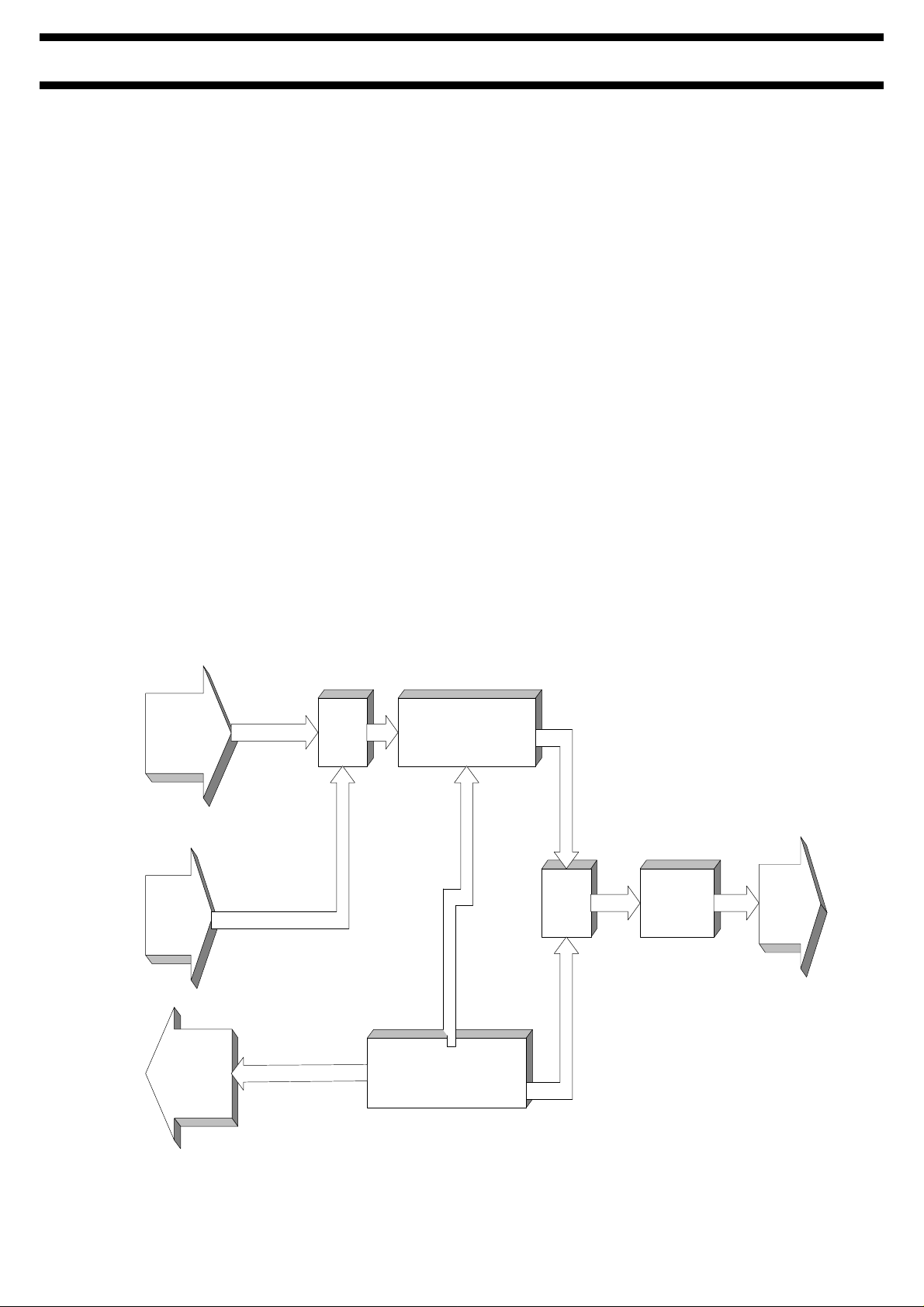
Sony Format Digital
Audio
Control from PIC micro
(Z211) on main pcb
Clock
SM5843AP1
Digital Filter,
Z14
SM5864 PWM
Noise Shaper, Z12
16.9344MHz Low-Jitter
System Clock, X1, Q5 & Z13
74HC74
Latches,
Z7 & Z8
Analogue Filter,
Z1, Z2, Z3, Z4
Audio out
Block Diagram of Alpha 8 DAC PCB
Page 3

ALPHA 7/8/9 CD SERVICE MANUALALPHA 7/8/9 CD SERVICE MANUAL
Test Points Marked on Circuit Diagram Only
Test Points Measurement Information
17MHz
AGND
AMUTE
CK
DA
CLKSYNC
DEEM
DGND
LOUT
LR
MUTERLY
N15
N18V
P5V(0)
P5V(1)
Clock Output to mother board. 16.9344MHz +/- 40ppm, 4V to 5V peak to peak square wave.
Analogue ground point.
Digital audio mute input on SK203. 0V=off, 5V=Mute.
Serial Data clock input on SK203. Sony format.
Serial Data data input on SK203. Sony format.
Crystal clock override. A 16.9344MHz HCMOS clock can be injected from an external source.
De-emphasis select input on SK203. 0V=off, 5V=On.
Digital ground point.
Left channel audio output at SK1. Measure d.c. offset at switch-on and after 1 minute, see specifications.
Serial Data LR input on SK203. Sony format.
Mute Relay Voltage. Equal to RLYPWR voltage when output is muted and 0V d.c. +0.5V,-0.0V when
output is un-muted.
Regulated analogue supply. -15V d.c. +/- 0.6V.
-18.45V d.c. +/- 0.5V supply input on SK204 for analogue.
+5V d.c. +/- 0.3V digital filter supply input on SK204.
+5V d.c. +/- 0.3V PWM noise shaper supply input on SK204.
P5VCLK
P15
P18V(0)
P18V(1)
PWRGND
RA0
RB0-RB7
REFL
REFR
RLYPWR
ROUT
SRVL
SRVR
SYSCLK
Regulated clock supply. +5V d.c. +/- 0.3V.
Regulated analogue supply. +15V d.c. +/- 0.6V.
+18.45V d.c. +/- 0.5V supply input on SK204 for analogue.
+18.45V d.c. +/- 0.5V supply input on SK204 for clock and latch.
Power ground point. Used by mute relay only.
Mute relay control from PIC micro on SK203.
Control lines from PIC micro on SK203.
DAC reference voltage, left channel. +5V +/- 0.3V.
DAC reference voltage, right channel.
+12V d.c. +/- 1V supply input for mute relay on SK204.
Right channel audio output at SK1. Measure d.c. offset at switch-on and after 1 minute, see
specifications.
Left d.c. servo voltage. -10 to +10V d.c.
Right d.c. servo voltage.
Clock used by latches. 4V to 5V peak to peak square wave at 16.9344MHz.
Page 4

ALPHA 7/8/9 CD SERVICE MANUALALPHA 7/8/9 CD SERVICE MANUAL
Disc Transport Module
The CDM 14 module comprises the disc loading
mechanism, laser assembly, RF amplifier and
analogue signal processing. All the servo control and
motor drive circuits are also included.
Digital Signal Processor
Mute, attenuation and de-emphasis functions are
controlled via a three-wire serial bus from the system
controller (Z212) to pins 26, 27 & 28 of the DAC
(Z201).
Digital audio is input to the DAC on pins 1, 2& 3 in
standard Sony format i.e. Word Clock, Data and Bit
Clock.
A digital output complying to the SPDIF standard is
generated by the decoder on the mechanisim
assembly. This is passed through an isolating
transformer, T202, to the digital output socket SK5.
System Controller
The CXP826P16Q system controller (Z212) is a
combined CD player controller, keyboard scanner,
remote control decoder and fluorescent display
driver. It's clock is generated by 4.00MHz resonator
X201.
The controller detects the position of the disc drawer
from the status of two microswitches, INSW &
OUTSW, on socket SK205. The drawer motor is
controlled via motor driver Z210
3. Unplug the unit from the mains.
4. Push the tray front upwards to remove it
from the tray. Push the tray in manually.
5. Remove the 4 screws holding the front panel
to the chassis and release the locating tabs.
6. Unplug the flexfoil from the display board
where it enters the main pcb.
7. Remove the 2 screws holding the remote
receiver pcb in place.
8. The front panel can now be pulled off the
unit.
9. To remove the display pcb remove the 6
screws holding the board in place.
To remove the main pcb first remove the DAC board
if it is an Alpha 8 or 9 CD player.
1. Remove the 3 screws holding the audio
output sockets to the rear panel and 2
screws holding the aluminium extrusion in
place.
2. Squeeze the tops of the 2 pcb pillars and lift
the board up slightly to clear them .
3. Remove the 2 flexfoils from the DAC board.
The DAC board, still attached to the extrusion, can
now be removed from the unit.
To remove the main pcb remove the 8 pcb securing
screws and the screw holding the digital ouput socket
to the chassis. (On Alpha 7 CDs also remove the 3
screws securing the audio ouput sockets in place).
Release the cables which connect the mechanism to
the main board.
The main pcb can now be slid out of the case.
The keyboard scanning works by connecting the keys
to a resistor ladder on an ADC (analogue to digital
convertor) input to the microcontroller. Pressing a
key presents a unique voltage to this input.
The signal from the remote control receiver is input
to RMIN (pin 2) after first passing through the PIC
microcontroller, Z211, on the small remote receiver
pcb. This PIC ic converts the RC-5 format codes
from the remote control handsets to NEC data,
suitable for the Sony chipset. It also controls
theconfiguration of the digital filter/DAC on the Alpha
8 and 9 DAC boards the The remote control data
contains a ‘customer code’ that identifies it as an
Arcam product.The microcontroller is confiqured to
accept this code by means of the diode network
D291 to D297.
Disassembly For Servicing
To remove the boards within the CD players follow
the instructions below.
1. Remove the top cover.
2. Press load to eject the CD tray.
Page 5
ALPHA 7/8/9 CD SERVICE MANUALALPHA 7/8/9 CD SERVICE MANUAL
Alpha 7/8/9 Main PCB Parts List
Ref. No. Description Part No.
C2 PPRO 680P 63V 5% RA 2D168
C3 PPRO 680P 63V 5% RA 2D168
C4 ELST NON POLAR 10UF 35V 2U610
C5 PPRO 100P 63V 5% RA 2D110N
C6 PPRO 680P 63V 5% RA 2D168
C7 PPRO 680P 63V 5% RA 2D168
C10 CERD 1N0 63V 2A210
C11 CERD 10N 100V 20% 2A310
C12 CERD 10N 100V 20% 2A310
C13 CERD 33P 63V 2A033
C14 CERD 33P 63V 2A033
C15 CERD 100P 63V 2A110
C16 CERD 100P 63V 2A110
C17 CERD 10N 100V 20% 2A310
C18 CERD 10N 100V 20% 2A310
C19 CERD 10N 100V 20% 2A310
C20 PPRO 680P 63V 5% RA 2D168
C21 ELST NON POLAR 10UF 35V 2U610
C22 ELST 100U 25V 2N710
C23 ELST 100U 25V 2N710
C24 ELST 100U 25V 2N710
C25 ELST 22U 20V OSCON 2P622
C26 ELST 100U 25V 2N710
C27 ELST 10U 50V 2N610
C28 CERD 470P 63V 2A147
C29 ELST 100U 25V 2N710
C32 CERD 10N 100V 20% 2A310
C33 ELST 1M0 25V 2N810
C34 ELST 100U 100V 2N710B
C35 ELST 100U 100V 2N710B
C36 ELST 3M3 25V 2N833
C37 ELST 10U 50V 2N610
C38 ELST 10U 50V 2N610
C39 ELST 100U 25V 2N710
C40 ELST 100U 25V 2N710
C41 ELST 100U 25V 2N710
C42 ELST 100U 25V 2N710
C43 ELST 1M0 25V 2N810
C44 ELST 1M0 25V 2N810
C45 ELST 1M0 25V 2N810
C46 ELST NON POLAR 10UF 35V 2U610
C47 ELST 1M0 25V 2N810
C48 ELST 1M0 25V 2N810
Alpha 7/8/9 Main PCB Parts List
Ref. No. Description Part No.
C49 ELST 10U 50V 2N610
C50 ELST 10U 50V 2N610
C51 ELST 1M0 25V 2N810
C52 CERD 10N 100V 20% 2A310
C53 ELST 22U 20V OSCON 2P622
C54 CERD 10N 100V 20% 2A310
C55 CERD 10N 100V 20% 2A310
C56 ELST 10U 50V 2N610
C102 PPRO 680P 63V 5% RA 2D168
C103 PPRO 680P 63V 5% RA 2D168
C104 ELST NON POLAR 10UF 35V 2U610
C105 PPRO 100P 63V 5% RA 2D110N
C291 CERD 47N 63V 10% 2A347
C292 ELST 100U 25V 2N710
C293 CERD 47N 63V 10% 2A347
C294 CERD 47N 63V 10% 2A347
D1 SSDIODE 1N4148 75V 3A4148
D2 SSDIODE 1N4148 75V 3A4148
D3 SSDIODE 1N4148 75V 3A4148
D4 RECTIFIER 1N4003F 1A 200V 3B4003
D5 RECTIFIER 1N4003F 1A 200V 3B4003
D6 RECTIFIER 1N4003F 1A 200V 3B4003
D7 RECTIFIER 1N4003F 1A 200V 3B4003
D8 RECTIFIER 1N4003F 1A 200V 3B4003
D9 RECTIFIER 1N4003F 1A 200V 3B4003
D10 RECTIFIER 1N4003F 1A 200V 3B4003
D11 RECTIFIER 1N4003F 1A 200V 3B4003
D12 RECTIFIER 1N4003F 1A 200V 3B4003
D13 RECTIFIER 1N4003F 1A 200V 3B4003
D14 RECTIFIER 1N4003F 1A 200V 3B4003
D15 RECTIFIER 1N4003F 1A 200V 3B4003
D16 RECTIFIER 1N4003F 1A 200V 3B4003
D17 ZENER 15V 400MW 3C11504
D18 ZENER 7V5 400MW 3C07504
D19 ZENER 4V7 400MW 3C04704
D20 ZENER 4V7 400MW 3C04704
D21 SSDIODE 1N4148 75V 3A4148
D22 RECTIFIER 1N4003F 1A 200V 3B4003
D23 RECTIFIER 1N4003F 1A 200V 3B4003
D291 SSDIODE 1N4148 75V 3A4148
D292 SSDIODE 1N4148 75V 3A4148
D293 SSDIODE 1N4148 75V 3A4148
D294 SSDIODE 1N4148 75V 3A4148
Page 6
ALPHA 7/8/9 CD SERVICE MANUALALPHA 7/8/9 CD SERVICE MANUAL
D295 SSDIODE 1N4148 75V 3A4148
D296 SSDIODE 1N4148 75V 3A4148
D297 SSDIODE 1N4148 75V 3A4148
DISP301 DISPLAY ALPHA 7/8/9 (SONY) B1008
F1 INS COVER PCB FUSEHOLDER F022
F1 FUSE 20mm 160mA T C11166
F1 / FUSEHOLDER 20mm PCB 8S004
F2 / FUSEHOLDER 20mm PCB 8S004
F2 INS COVER PCB FUSEHOLDER F022
F4 FUSE 20mm 160mA T C11166
F4 SPARE FUSEHOLDER F062
HS1 HEATSINK TO220 CLIP 30 F007
HS2 HEATSINK TO220 8.6 DEGC/W F008
HS2 HEATSINK CLIP TO220 13/8.6 DC/W F006
L1 FERRITE BEAD SINGLE AXIAL TAPED 2K BOX 7F003
L2 INDUCT 1R0 283AS-1R0K 34-10914 7D001
L3 INDUCT 1R0 283AS-1R0K 34-10914 7D001
L4 33UH IND 34-48330 7D033
L5 33UH IND 34-48330 7D033
L6 6U8H INDUCTOR 7D968A
L7 6U8H INDUCTOR 7D968A
LED201 LED RED 5MM 3D5119
LED301 LED GREEN 5MM 3D001
LK101A JUMPER 4-WAY LEAD L814CA
PAD1 Alpha 7/8/9 CD SUPPORT PAD E805AP
PL1 16 WAY DIL PIN HEADER 8K6316
Q1 TRANS LF SS N BC547B 4A547
Q2 TRANS LF SS N BC547B 4A547
Q3 TRANS LF SS P BC557B 4A557
Q4 TRANS LF SS N BC547B 4A547
Q5 TRANS LF SS N BC547B 4A547
Q6 TRANS LF SS N BC547B 4A547
Q101 TRANS LF SS N BC547B 4A547
R2 RES MF W4 3K9 1% 1H239
R3 RES MF W4 3K9 1% 1H239
R4 RES MF W4 3K9 1% 1H239
R5 RES MF W4 1% 10K 1H310
R6 RES MF W4 1% 10K 1H310
R7 RES MF W4 1% 33K 1H333
R8 RES MF W4 3K9 1% 1H239
R9 RES MF W4 3K9 1% 1H239
R10 RES MF W4 22K 1% 1H322
R11 RES MF W4 120R 1% 1H112
R12 RES MF W4 22R 1% 1H022
R13 RES MF W4 1% 10K 1H310
R14 RES MF W4 1% 10K 1H310
R15 RES MF W4 1% 10K 1H310
R16 RES MF W4 330R 1% 1H133
R17 RES MF W4 1% 10K 1H310
R18 RES MF W4 1% 33K 1H333
R19 RES MF W4 1% 33K 1H333
R20 RES MF W4 22R 1% 1H022
R21 RES MF W4 470R 1% 1H147
R22 RES MF W4 1% 220R 1H122
R23 RES MF W4 120R 1% 1H112
R24 RES MF FU W3 5% 10R NFR25 1G010
R25 RES MF W4 120R 1% 1H112
R26 RES MF W4 100K 1% 1H410
R27 RES MF W4 100K 1% 1H410
R28 RES MF W4 1% 10K 1H310
R29 RES MF W4 1% 1K0 1H210
R30 RES MF W4 1% 10K 1H310
R31 RES MF W4 330R 1% 1H133
R32 RES MF W4 330R 1% 1H133
R33 RES MF W4 330R 1% 1H133
R34 RES MF W4 1% 10K 1H310
R35 RES MF W4 4M7 1% 1H547
R36 RES MF W4 1% 620R 1H162
R37 RES MF FU W3 5% 10R NFR25 1G010
R38 RES MF W4 330R 1% 1H133
R39 RES MF W4 1% 220R 1H122
R40 RES MF W4 1% 220R 1H122
R41 RES MF W4 1K6 1% 1H216
R42 RES MF W4 1% 1K0 1H210
R43 RES MF W4 330R 1% 1H133
R44 RES MF FU W3 5% 3R3 NFR25 1G833
R45 RES MF FU W3 5% 3R3 NFR25 1G833
R46 RES MF W4 3K0 1% 1H230
R47 RES MF W4 3K0 1% 1H230
R48 RES MF FU W3 5% 10R NFR25 1G010
R49 RES MF W4 120R 1% 1H112
R50 RES MF W4 100K 1% 1H410
R51 RES MF FU W3 22R 5% NFR25 1G022
R52 RES MF FU W3 22R 5% NFR25 1G022
R53 RES MF W4 1% 33K 1H333
R54 RES MF W4 330R 1% 1H133
R55 RES MF W4 1% 680R 1H168
R56 RES MF W4 330R 1% 1H133
R57 RES MF W4 330R 1% 1H133
R58 RES MF FU W3 5% 10R NFR25 1G010
Page 7

ALPHA 7/8/9 CD SERVICE MANUALALPHA 7/8/9 CD SERVICE MANUAL
R59 RES MF W4 330R 1% 1H133
R60 RES MF W4 1% 8K2 1H282
R61 RES MF W4 1% 8K2 1H282
R62 RES MF W4 330R 1% 1H133
R63 RES MF W4 1% 33K 1H333
R64 RES MF FU W3 5% 10R NFR25 1G010
R102 RES MF W4 3K9 1% 1H239
R103 RES MF W4 3K9 1% 1H239
R104 RES MF W4 3K9 1% 1H239
R105 RES MF W4 1% 10K 1H310
R106 RES MF W4 1% 10K 1H310
R107 RES MF W4 1% 33K 1H333
R108 RES MF W4 3K9 1% 1H239
R109 RES MF W4 3K9 1% 1H239
R110 RES MF W4 22K 1% 1H322
R111 RES MF W4 120R 1% 1H112
R112 RES MF W4 22R 1% 1H022
R113 RES MF W4 1% 10K 1H310
R291 RES MF FU W3 5% 3R3 NFR25 1G833
R292 RES MF W4 1% 8K2 1H282
R293 RES MF W4 1% 8K2 1H282
R294 RES MF W4 1% 1K0 1H210
R295 RES MF W4 1% 10K 1H310
R296 RES MF W4 1% 10K 1H310
R297 RES MF W4 1% 10K 1H310
R298 RES MF W4 1% 10K 1H310
R301 RES MF W4 1% 33K 1H333
R302 RES MF W4 1% 12K 1H312
R303 RES MF W4 1% 5K6 1H256
R304 RES MF W4 1% 3K3 1H233
R305 RES MF W4 1% 2K2 1H222
R306 RES MF W4 1% 1K5 1H215
R307 RES MF W4 1% 1K2 1H212
R308 RES MF W4 1% 8K2 1H282
R309 RES MF W4 1% 3K3 1H233
R310 RES MF W4 1% 2K2 1H222
R311 RES MF W4 1% 1K5 1H215
R312 RES MF W4 1% 1K2 1H212
R313 RES MF W4 1% 8K2 1H282
R314 RES MF W4 1% 220R 1H122
RX201 REMOTE CONTROL RX SBX1610-62 38KHZ B2103
SH1 PHONO EMC SHIELD E808MC
SK1 IEC MAINS 2-PIN PCB 8A014
SK2 8+8 WAY FEMALE HORIZ SKT 8K6416
SK4 PHONO SKT 2-WAY HOR EMC 8D222
SK5 PHONO SKT SINGLE EMC 8D220
SK201 23-WAY FFC CONN VERT 8K8023
SK203 32-WAY FFC CONN VERT 8K8032
SK204 23-WAY FFC CONN VERT 8K8023
SK205 5-WAY AMP CT CONN 8K2005
SK291 32-WAY FFC CONN VERT 8K8032
SK301 32-WAY FFC CONN HORIZ 8K8132
SW201 SW PUSH 4PCO A1014
SW301 TACT SWITCH 2-PIN LOW PROF A1504
SW302 TACT SWITCH 2-PIN LOW PROF A1504
SW303 TACT SWITCH 2-PIN LOW PROF A1504
SW304 TACT SWITCH 2-PIN LOW PROF A1504
SW305 TACT SWITCH 2-PIN LOW PROF A1504
SW306 TACT SWITCH 2-PIN LOW PROF A1504
SW307 TACT SWITCH 2-PIN LOW PROF A1504
SW308 TACT SWITCH 2-PIN LOW PROF A1504
SW309 TACT SWITCH 2-PIN LOW PROF A1504
SW310 TACT SWITCH 2-PIN LOW PROF A1504
SW311 TACT SWITCH 2-PIN LOW PROF A1504
SW312 TACT SWITCH 2-PIN LOW PROF A1504
T201 ALPHA 7 CD MAINS TRANSFORMER L811TX
T202 DIGITAL OUTPUT COUPLER K 7E015
X1 CRYSTAL 16.9344MHz PARALLEL 7X012
X201 CER RESON 4.00MHz 7W005
Z1 IC OPAMP DUAL NJM2114D 5B2114
Z101 IC OPAMP DUAL NJM2114D 5B2114
Z201 IC CD DAC PCM1710U 5G1710
Z202 IC HCMOS 74HCU04 5J7404
Z203 IC VREG POS 78L05 5D78L05
Z204 IC VREG POS LM317T 5D317T
Z205 IC VREG POS LM337T 5D337
Z206 IC VREG POS LM317T 5D317T
Z207 IC VREG POS LM317T 5D317T
Z208 IC VREG POS 7805 5D7805
Z209 IC VREG NEG 7915 5D7915
Z210 IC MOTOR DRIVER LB1641 5Q1641
Z211 IC CMOS MICRO PIC16C54XT/P 5H16C54X
Z211 IC SOCKET 18 PIN 0.3'' 8S018
Z212 IC CD CXP826P16Q MICRO 5G826
Page 8

ALPHA 7/8/9 CD SERVICE MANUALALPHA 7/8/9 CD SERVICE MANUAL
Alpha 8 DAC PCB Only Parts List
Ref. No. Description Part No.
C1 PPRO 2N7 63V 5% RA 2D227
C2 PPRO 2N7 63V 5% RA 2D227
C3 PPRO 2N7 63V 5% RA 2D227
C4 PPRO 2N7 63V 5% RA 2D227
C5 PPRO 2N7 63V 5% RA 2D227
C6 PPRO 2N7 63V 5% RA 2D227
C7 PPRO 1N0 63V 5% RA 2D210
C8 PPRO 1N0 63V 5% RA 2D210
C9 PPRO 1N0 63V 5% RA 2D210
C10 PPRO 1N0 63V 5% RA 2D210
C11 PPRO 1N0 63V 5% RA 2D210
C12 PPRO 1N0 63V 5% RA 2D210
C13 PPRO 470P 63V 5% RA 2D147N
C14 PPRO 470P 63V 5% RA 2D147N
C15 PPRO 470P 63V 5% RA 2D147N
C16 PPRO 470P 63V 5% RA 2D147N
C17 MLC 100P 100V NPO 5% SM 2C110
C18 ELST 10U 50V 2N610
C19 ELST 10U 50V 2N610
C20 PPRO 1N3 63V 5% RA 2D213N
C21 ELST 10U 50V 2N610
C22 PCRB 100N 100V 5% RA 5mm 2H410
C23 ELST 10U 50V 2N610
C24 ELST NON POLAR 10UF 35V 2U610
C25 ELST NON POLAR 10UF 35V 2U610
C26 PPRO 4N7 63V 5% RA 2D247N
C27 PCRB 100N 100V 5% RA 5mm 2H410
C29 ELST 10U 50V 2N610
C30 PPRO 4N7 63V 5% RA 2D247N
C34 MLC 10N 50V X7R 10% SM 2C310
C35 MLC 470P 100V NPO 5% SM 2C147
C36 MLC 470P 100V NPO 5% SM 2C147
C37 MLC 10N 50V X7R 10% SM 2C310
C38 MLC 10N 50V X7R 10% SM 2C310
C39 MLC 10N 50V X7R 10% SM 2C310
C40 MLC 10N 50V X7R 10% SM 2C310
C41 MLC 10N 50V X7R 10% SM 2C310
C42 PPRO 470P 63V 5% RA 2D147N
C43 PPRO 470P 63V 5% RA 2D147N
C44 PPRO 470P 63V 5% RA 2D147N
C45 PPRO 470P 63V 5% RA 2D147N
C46 MLC 100P 100V NPO 5% SM 2C110
C47 MLC 47P 100V NPO 5% SM 2C047
Alpha 8 DAC PCB Only Parts List
Ref. No. Description Part No.
C49 ELST 22U 20V OSCON 2P622
C50 ELST 22U 20V OSCON 2P622
C53 ELST 220U 16V 2N722
C55 MLC 100N 50V X7R 10% SM 2C410
C56 ELST 100U 25V 2N710
C57 ELST 100U 25V 2N710
C58 ELST NON POLAR 10UF 35V 2U610
C59 ELST NON POLAR 10UF 35V 2U610
C60 PPRO 4N7 63V 5% RA 2D247N
C61 PPRO 4N7 63V 5% RA 2D247N
C62 MLC 10N 50V X7R 10% SM 2C310
C63 ELST 470U 25V RA 2N747
C64 ELST 470U 25V RA 2N747
C65 MLC 10N 50V X7R 10% SM 2C310
C66 ELST NON POLAR 2.2UF 50V 2V522
C67 ELST NON POLAR 2.2UF 50V 2V522
C68 MLC 10N 50V X7R 10% SM 2C310
C69 MLC 33P 100V NPO 5% SM 2C033
D1 SSDIODE 1N4148 75V 3A4148
D2 SSDIODE 1N4148 75V 3A4148
L1 33UH IND SM 1812 180mA 7B033
L2 33UH IND SM 1812 180mA 7B033
L3 33UH IND SM 1812 180mA 7B033
L4 33UH IND SM 1812 180mA 7B033
L5 33UH IND SM 1812 180mA 7B033
L6 2U2H INDUCTOR 7D922
Q1 TRANS LF SS N SM BC847B 4A847
Q3 TRANS LF SS N SM BC847B 4A847
Q5 TRANS LF SS N SM BC847B 4A847
Q6 TRANS LF SS N SM BC847B 4A847
Q8 TRANS LF SS N SM BC847B 4A847
Q9 TRANS LF SS N SM BC847B 4A847
Q11 TRANS MOSFET SW ZVNL120A 4K120
R1 RESISTOR SM W4 1K0 2% 1A210
R2 RESISTOR SM W4 1K0 2% 1A210
R3 RESISTOR SM W4 1K0 2% 1A210
R4 RESISTOR SM W4 1K0 2% 1A210
R5 RESISTOR SM W4 1K0 2% 1A210
R6 RESISTOR SM W4 1K0 2% 1A210
R7 RESISTOR SM W4 1K0 2% 1A210
R8 RESISTOR SM W4 1K0 2% 1A210
R9 RESISTOR SM W4 2K2 2% 1A222
R10 RESISTOR SM W4 2K2 2% 1A222
Page 9

ALPHA 7/8/9 CD SERVICE MANUALALPHA 7/8/9 CD SERVICE MANUAL
R11 RESISTOR SM W4 2K2 2% 1A222
R12 RESISTOR SM W4 2K2 2% 1A222
R13 RESISTOR SM W4 2K2 2% 1A222
R14 RESISTOR SM W4 2K2 2% 1A222
R15 RESISTOR SM W4 2K2 2% 1A222
R16 RESISTOR SM W4 2K2 2% 1A222
R17 RES MF FU W3 10R 5% NFR25 1G010
R18 RESISTOR SM W4 10R 2% 1A010
R19 RESISTOR SM W4 47K 2% 1A347
R20 RESISTOR SM W4 47K 2% 1A347
R21 RES MF FU W3 100R 5% NFR25 1G110
R25 RESISTOR SM W4 0R0 2% 1A000
R34 RESISTOR SM W4 0R0 2% 1A000
R35 RESISTOR SM W4 100R 2% 1A110
R36 RESISTOR SM W4 100R 2% 1A110
R37 RESISTOR SM W4 100R 2% 1A110
R38 RESISTOR SM W4 100R 2% 1A110
R39 RESISTOR SM W4 220R 2% 1A122
R40 RESISTOR SM W4 100R 2% 1A110
R41 RESISTOR SM W4 220R 2% 1A122
R42 RESISTOR SM W4 0R0 2% 1A000
R43 RESISTOR SM W4 100R 2% 1A110
R44 RESISTOR SM W4 100R 2% 1A110
R45 RES MF W4 1K2 1% 1H212
R46 RES MF W4 1K2 1% 1H212
R47 RES MF W4 1K2 1% 1H212
R48 RES MF W4 1K2 1% 1H212
R49 RES MF W4 3K3 1% 1H233
R50 RES MF W4 3K3 1% 1H233
R51 RES MF W4 3K3 1% 1H233
R52 RES MF W4 3K3 1% 1H233
R53 RESISTOR SM W4 1K0 2% 1A210
R54 RESISTOR SM W4 1K0 2% 1A210
R55 RESISTOR SM W4 4K7 2% 1A247
R56 RESISTOR SM W4 11K 2% 1A311
R57 RESISTOR SM W4 11K 2% 1A311
R58 RESISTOR SM W4 18K 2% 1A318
R59 RESISTOR SM W4 18K 2% 1A318
R64 RESISTOR SM W4 47R 2% 1A047
R65 RESISTOR SM W4 47R 2% 1A047
R66 RESISTOR SM W4 100K 2% 1A410
R67 RESISTOR SM W4 470R 2% 1A147
R68 RESISTOR SM W4 10K 2% 1A310
R69 RESISTOR SM W4 10K 2% 1A310
R72 RESISTOR SM W4 100R 2% 1A110
R73 RESISTOR SM W4 100R 2% 1A110
R74 RESISTOR SM W4 100R 2% 1A110
R75 RESISTOR SM W4 100R 2% 1A110
R80 RESISTOR SM W4 2K2 2% 1A222
R81 RESISTOR SM W4 2K2 2% 1A222
R82 RESISTOR SM W4 680K 2% 1A468
R84 RESISTOR SM W4 680K 2% 1A468
R85 RESISTOR SM W4 680K 2% 1A468
R86 RESISTOR SM W4 0R0 2% 1A000
R91 RESISTOR SM W4 0R0 2% 1A000
R92 RESISTOR SM W4 0R0 2% 1A000
R94 RESISTOR SM W4 220R 2% 1A122
R95 RESISTOR SM W4 220R 2% 1A122
R96 RESISTOR SM W4 2K4 2% 1A224
R97 RESISTOR SM W4 2K4 2% 1A224
R98 RESISTOR SM W4 0R0 2% 1A000
R99 RESISTOR SM W4 0R0 2% 1A000
R102 RESISTOR SM W4 0R0 2% 1A000
R103 RESISTOR SM W4 0R0 2% 1A000
R104 RES MF W4 1K2 1% 1H212
R108 RESISTOR SM W4 100K 2% 1A410
R109 RESISTOR SM W4 100K 2% 1A410
R110 RESISTOR SM W4 100K 2% 1A410
R111 RESISTOR SM W4 100K 2% 1A410
R112 RESISTOR SM W4 680K 2% 1A468
R113 RESISTOR SM W4 680K 2% 1A468
R114 RESISTOR SM W4 100K 2% 1A410
R115 RESISTOR SM W4 0R0 2% 1A000
R117 RESISTOR SM W4 0R0 2% 1A000
RLY1 RELAY 960 OHM 51SB12T A205
SH1 PHONO EMC SHIELD E808MC
SK1 PHONO SKT 4-WAY EMC GOLD 8D225
SK203 32-WAY FFC CONN VERT 8K8032
SK204 23-WAY FFC CONN VERT 8K8023
X1 CRYSTAL 16.9344MHz PARALLEL 7X012
X1 GROMMET 8 I/D X 6.5 THK F021
Z1 IC OPAMP SM OP27 5B027S
Z2 IC OPAMP SM OP27 5B027S
Z3 IC AUDIO DUAL SM 4560D 5B4560M
Z4 IC AUDIO DUAL SM 4560D 5B4560M
Z5 IC VREG POS 78L05 5D78L05
Z7 IC HCMOS SM 74HC74 5K7474
Z8 IC HCMOS SM 74HC74 5K7474
Z11 IC VREG POS 78L05 5D78L05
Z12 IC CMOS SDECO DAC SM5864AP 5G5864
Page 10

ALPHA 7/8/9 CD SERVICE MANUALALPHA 7/8/9 CD SERVICE MANUAL
Z13 IC HCMOS SM 74HCU04 5K7404
Z14 IC DIGITAL FILT SM5843APT 5G5843
Z16 IC VREG POS LM317T 5D317T
Z17 IC VREG POS LM337T 5D337
Z18 IC AUDIO DUAL SM 4560D 5B4560M
Alpha 7/8/9 CD Non PCB Parts, Metalwork etc.
Part No. Description
B3002 BATTERY AA
B2009 CDM14 MECHANISM
E802CH CHASSIS
E802CP ALPHA 7/8/9 CD/TUNER COVERPLATE
E802MI PCB INSULATOR
E806RP REAR PANEL
E810FP ALPHA 7/8 TUNER FASCIA
E813PM CD DRAWER FRONT
E815PM POWER BUTTON
E822PM FOOT
E823PM ALPHA 7 BADGE
E824PM ALPHA 8 BADGE
E825PM ALPHA 9 BADGE
HP006 SNAP RIVET (HOLDS MECH IN PLACE)
L801RC CR14 REMOTE CONTROL HANSET
L807CA FLEX FOILS MAIN BOARD TO DAC PCB
SH054 OWNERS HANDBOOK
SH058 WARRANTY LEAFLET
Page 11

ALPHA 7/8/9 CD PLAYER MAIN PRINTED CIRCUIT BOARD LAYOUTALPHA 7/8/9 CD PLAYER MAIN PRINTED CIRCUIT BOARD LAYOUT
Page 12

ALPHA 8 CD PLAYER DAC PRINTED CIRCUIT BOARD LAYOUT (underside view)ALPHA 8 CD PLAYER DAC PRINTED CIRCUIT BOARD LAYOUT (underside view)
Page 13

ALPHA 8 CD PLAYER DAC PRINTED CIRCUIT BOARD LAYOUT (top view)ALPHA 8 CD PLAYER DAC PRINTED CIRCUIT BOARD LAYOUT (top view)
Page 14

87654321
LK1
LINK10NP
D
C
LK11
LINK10NP
LK21
LINK10NP
LK31
LINK10NP
LK41
LINK10NP
LK51
LINK10NP
LK61
LINK10NP
LK71
LINK10NP
LK81
LINK10NP
LK91
LINK10NP
LK2
LINK10NP
LK12
LINK10NP
LK22
LINK10NP
LK32
LINK10NP
LK42
LINK10NP
LK52
LINK10NP
LK62
LINK10NP
LK72
LINK10NP
LK82
LINK10NP
LK92
LINK10NP
LK3
LINK10NP
LK13
LINK10NP
LK23
LINK10NP
LK33
LINK10NP
LK43
LINK10NP
LK53
LINK10NP
LK63
LINK10NP
LK73
LINK10NP
LK83
LINK10NP
LK93
LINK10NP
LK4
LINK10NP
LK24
LINK10NP
LK34
LINK10NP
LK44
LINK10NP
LK54
LINK10NP
LK64
LINK10NP
LK74
LINK10NP
LK84
LINK10NP
LK94
LINK10NP
LK5
LINK10NP
LK15
LINK10NP
LK25
LINK10NP
LK35
LINK10NP
LK45
LINK10NP
LK55
LINK10NP
LK65
LINK10NP
LK75
LINK10NP
LK85
LINK10NP
LK95
LINK10NP
LK6
LINK10NP
LK16
LINK10NP
LK26
LINK10NP
LK36
LINK10NP
LK46
LINK10NP
LK56
LINK10NP
LK76
LINK10NP
LK86
LINK10NP
LK96
LINK10NP
LK7
LINK10NP
LK17
LINK10NP
LK27
LINK10NP
LK37
LINK10NP
LK47
LINK10NP
LK57
LINK10NP
LK67
LINK10NP
LK77
LINK10NP
LK87
LINK10NP
LK97
LINK10NP
LK8
LINK10NP
LK18
LINK10NP
LK28
LINK10NP
LK38
LINK10NP
LK48
LINK10NP
LK58
LINK10NP
LK68
LINK10NP
LK78
LINK10NP
LK88
LINK10NP
LK9
LINK10NP
LK19
LINK10NP
LK29
LINK10NP
LK39
LINK10NP
LK49
LINK10NP
LK59
LINK10NP
LK69
LINK10NP
LK79
LINK10NP
LK89
LINK10NP
Links
LK10
LINK10NP
LK20
LINK10NP
LK30
LINK10NP
LK40
LINK10NP
LK50
LINK10NP
LK60
LINK10NP
LK70
LINK10NP
LK80
LINK10NP
LK90
LINK10NP
Power Supplies
L812C2_8.SCH
DAC & Audio outputs
L812C3_8.SCH
INOUT
LDIN
LDOUT
4MHZ
FILA
FILB
Microcontroller & Display
L812C4_8.SCH
INOUT
LDIN
LDOUT
4MHZ
FILA
FILB
DEEM
SMUTE
AMUTE
RMIN
PGML
CLK
DATA
SCOR
SQCK
XRST
LDON
XLT
SENSE
SUBQ
D
K0
K1
K0
K1
C
DD
Drilling
Detail
DRILL_DETAIL
B
A
1 2 3 4 5 6 7 8
TL1
TOOLING3.0
PAD1
VFD SUPPORT PAD
ACD_VFD_PAD
A2
Update Box
UPDATE_BOX
TL2
TOOLING4.1
Tooling Holes & Alignment Marks
PS
Photo Strip
PHOTO_STRIP
Documentation
TL3
TOOLING3.0
F4
T160MASP
Spare Fuse
TL4
TOOLING3.0
A1
BARCODE LABEL
BARCODE_A7CD
TL5
TOOLING3.0
A3
BARCODE_A8CD
FD_1
FIDUCIAL
BARCODE LABEL
FD_2
FIDUCIAL
23425
A & R Cambridge Ltd.
Pembroke Avenue
Denny Industrial Centre
Waterbeach
Cambridge CB5 9PB
DRAWING TITLE
Alpha 7 CD Project Sheet
Circuit Diagram
1 4Sheet of
Filename
J:\FILES\PCBS\CIRCUITS\L812C1_8.PRJ
30-Oct-1997
CAH 96_1039
CAH 96_1104
CAH 24-4-97 UPGRADE IMPROVEMENTS97_1037 6
CAH 97_1069 2-9-97 HDCD LED changed
CAH 97_1101 30-10-97 HDCD LED removed from Alpha 7 CD
DRAWN BY CHK BY
ECO No.
DATE
C38 was 100U EL. LK14 removed & R64 added25 June 1996
LK66 removed & R65 added20 Nov 1996
L812CT 8
DESCRIPTION OF CHANGE
B
4
A
5
7
ISSUEDRAWING NO.
Page 15

Spare fuseSpare fuseSpare fuseSpare fuse
D
C
B
100U EL
RIV1
HP007
LIVE NEUT
L3
1U0H RADIAL
L6
6U8H RADIAL
C41
RIV2
HP007 + C49
SK1
IEC2
NL
L2
1U0H RADIAL
F2
T250MA115V
115V units only
F1
T160MA
230V units only
FILB
FILB
FILA
FILA
P7V
+
C55
10N CD
L7
6U8H RADIAL
!
!
R51 22R FU
R52
NEUT2
115V
230V
!
!
22R FU
115V
230V
10
O/P 'Out'
10
SW201B
A1014
4
FILAC
11
9
1
2
7
6
4
5
10
9
SW201D
12
Vcc
8
5
T201
L811TX
A1014
Vcc
7
6
Z210
LB1641
LoadOut
6
16
17
ACAUD2
18
11
AC1
AC
AC2
13
ACDIG2
15
19
20
LoadIn
5
ACAUDG
ACAUD1
ACDIG1
ACDIG3
FILASW
Bias
4
C32
10N CD
87654321
SK204
GND
RB3
RB7
Vout
HS
RB0
RB1
RB2
RB3
RB4
RB5
RB6
RB7
23
22
21
20
19
18
17
16
15
14
13
12
11
10
9
8
7
6
5
4
3
2
1
FFC23V
O
TP2TP3 TP4
+ C42
100U EL
P5V
C54
10N CD
PD1
PAD300/4.1
D
C
B
D16
Vin
Vin
R64
!
1
2
3
4
L814CA
1N4003F
Vout
ADJ
A
+ C39
100U EL
+ C40
100U EL
A
ADJ
Vout
HS4TO220HS30REG
D15 1N4003F
P11V CLK
!
I
+ C51
1M0 25V
GND5VDAC
TP1
LK101B
LK101A
L814CA
O
O
Z207
LM317T
Vin
1
2
3
4
R39
220R MF
R47
3K0 MF
R46
3K0 MF
R40
220R MF
A
P5V
HDCD
TP6
D14
1N4003F
Vout
ADJ
+ C38
10U EL
REMIN
HDCD
TP5
+ C50
P18V
100U EL
100U EL
N18V
O
RA0
P18V
N18V
R43
330R MF
R42
1K0 MF
RA0
AMUTE
DEEM
RMIN
XRST
4MHZ
AC1
AC
AC2
DAC Supply
+5V
P5V
R27
R50
100K MF
R54
330R MF
R59
330R MF
D22
1N4003F
D23
1N4003F
P5VDAC
C46
10U NP
100K MF
P11V
17
18
1
2
3
4
!
R37 10R FU
!
Z211
PIC16C54XT
RA0
RA1
RA2
RA3
RTCC
MCLR
OSC1
16
R48
10R FU
+
1M0 25V
OSC2
15
+ C56
C33
RLYV
10U EL
5
TO220HS08REG
RB0
RB1
RB2
RB3
RB4
RB5
RB6
RB7
VSS
14
VDD
P22VUN
!
R44 3R3 FU
1M0 25V
!
3R3 FU
O
R53
33K MF
D18
7V5 400MW
N30V
GND
1
C47
1M0 25V
N22VUN
P11V
CDM14 Supply
+7.3V
R38
330R MF
R41
1K6 MF
TP7
3
+5V
O/P
Case
C44
C45
1M0 25V
Z206 LM317T
I
GNDREM
1M0 25V
Vin
O
AGND
D4
UF4003
D6
UF4003
D8
UF4003
D10
UF4003
DGND
D12
1N4003F
!
R58 10R FU
GND
O/P 'In'
1
2
3
D5
UF4003
D7
UF4003
D9
UF4003
D11
UF4003
+
C34
100U EL 100V
N35V
SW201C
A1014
+
C36
3M3 EL
I
Vin
Z209
7915
HDCDREM
LED201
LED ULTRARED
Alpha 8 only
9
8
7
P11VSW
TO220HS30REG
D17
15V 400MW
G
GND
HS1
Vout
+
+
R45
D13
1N4003F
Vout
ADJ
A
+ C37
10U EL
C35
100U EL 100V
+
N30V
RX201
SBX1610-52
C52
10N CD
Z204
LM317T
I
HS3
TO220HS30REG
+
+C48
Z205
LM337T
I
R65 10R FU
P7V P5VP5V DAC
10R FU
P7V
+
C43
1M0 25V
P5VREM
REMOUT
2
I
HS2A
+
P5V DAC
Vin
6
RB0
7
8
9
10
RB4
11
12
13
P5V
C53
22U EL OS
P18V
N18V
P5V
P11V
Power connector to DAC PCB
Z208 7805
G
RB1
RB2
RB5
RB6
LDOUT
A
1 2 3 4 5 6 7 8
LDIN
INOUT
R55
1K2 MF
OUTSW
D19
LOADOUT
LOADININSW
4V7 400MW
SK205
8K2005
1
2
LOADOUT
3
LOADIN
4
GND
5
INSW
OUTSW
Motor Ground
23425
A & R Cambridge Ltd.
Pembroke Avenue
Denny Industrial Centre
Waterbeach
Cambridge CB5 9PB
DRAWING TITLE
Alpha 7/8/9 CD Players
Circuit Diagram
2 4Sheet of
Filename
J:\FILES\PCBS\CIRCUITS\L812C2_8.SCH
30-Oct-1997
CAH 96_1039
CAH 96_1104
CAH 24-4-97 UPGRADE IMPROVEMENTS97_1037 6
CAH 97_1069 2-9-97 HDCD LED changed
CAH 97_1101 30-10-97 HDCD LED removed from Alpha 7 CD
DRAWN BY CHK BY
ECO No.
DATE
C38 was 100U EL. LK14 removed & R64 added25 June 1996
LK66 removed & R65 added20 Nov 1996
L812CT 8
DESCRIPTION OF CHANGE
4
A
5
7
ISSUEDRAWING NO.
Page 16

87654321
Alpha 7 CD Configuration Plug
SK2
1 2
3 4
5 6
7 8
9 10
11 12
13 14
D
15 16
DIL16 HSKT
D
Flex connector from CDM14 mech
SK201
ADATA
FFC23V
P11V CLK
23
SUBQ
22
SENSE
21
XLT
20
LDON
19
18
P5V
17
16
DIGOUT
15
14
XRST
13
AMUTE
12
SQCK
11
SCOR
10
DATA
9
CLK
8
BCLK
7
ADATA
6
LRCK
5
WDCK
4
3
2
1
17MHZ
WDCK 17MHZ
LRCK
ADATA
BCLK
R49
120R MF
Z202A 74HCU04
Z202B 74HCU04
Z202C 74HCU04
1 2 3 4 5 6 7 8
SCLK
FOK
GFS
C
BCLK
LRCK
P7V
B
A
TP10
SMUTE
XRST
TP8
TP9
12
34
56
WD
R16
P5V DAC
LRCK
ADATA
BCLK
I
+ C26
100U EL
L4
33UH AX
330R MF
Z203
78L05
Vin
C12
10N CD
P5V DAC(A7)
PL1
DIL16 VPLG
GND
G
P5V DAC(A7)
R23
120R
C24
100U EL
+
12
34
56
78
910
1112
1314
1516
Vout
C25
22U EL OS
O
17MHZ
P5VCLK
+
A7DAC5V
PGML
CLK
DATA
R31 330R MF
R32 330R MF
C28
1N0 PP
R62
330R MF
TP14
74HCU04
7
R33 330R MF
18
19
20
21
22
23
24
25
26
27
28
Vdd
CKSL
MUTE
MD/DM1
TP11
Z202F
74HCU04
X1
C13
33P CD
MODE
Z201
PCM1710U
R25
120R MF
Z202D
8 9
74HCU04
1213
ML/DSD
MC/DM2
LRCIN1DIN2BCKIN3CLKO4XTI5XTO6DGND7Vdd8Vcc2R9AGND2R10EXT1R11EXT2R12VOUTR13AGND
17MHz
14
Z202G
16.9344MHZ
DGND
C11
680P PP
Analogue ground
R19
33K MF
R18
33K MF
Vcc2L
AGND2L
R57
330R MF
100P CD
C15
100P CD
C16
!
R24
10R FU
C23
+
100U EL
15
16
17
EXT2L
EXT1L
VOUTL
14
+
C22
100U EL
10 11
Z202E 74HCU04
R35
4M7 MF
10N CD
BC547B
R21
470R MF
12345678910111213141516171819202122232425262728293031
SK203
FFC32V
L5
33UH AX
VOUTL
Vcc
C20
680P PP
DACGND
R56
330R MF
C17
Q2
C10
1N0 CD
23425
A & R Cambridge Ltd.
Pembroke Avenue
Denny Industrial Centre
Waterbeach
Cambridge CB5 9PB
HDCD
C21
10U NP
NOT FITTED
D21
1N4148
RB3
RB2
PMUTE
R2
3K9 MF
C1
NOT FITTED
AUDGND
R102
3K9 MF
VOUTR
C101
P5V
R17
10K MF
22R MF
XRST
+ C29
100U EL
DEEM
SMUTE
RA0
RB7
RB6
RB5
RB4
RB0
RB1
Data connector to DAC PCB
R4
D1
1N4148
SW201A
A1014
R28
10K MF
3K9 MF
R5
10K MF
R104
3K9 MF
R105
10K MF
PMUTE
3
2
3
2
PMUTE
10K MF
680P PP
R3
3K9 MF
C3
680P PP
680P PP
R103
3K9 MF
C103
680P PP
R20
C2
C102
1
2
3
DRAWING TITLE
Alpha 7,8 & 9 CD Players
Circuit Diagram
3 4Sheet of
Filename
J:\FILES\PCBS\CIRCUITS\L812C3_8.SCH
DIGOUT
R34
BC547B
Q6
WD
AMUTE
XRST
Z1A
NJM2114
1
Z101A
NJM2114
1
Analogue Ground
P5V
Q5
BC547B
30-Oct-1997
LRCK
DIGOUT
17MHZ
ADATA
BCLK
32
LEFT1
R6
10K MF
R7
33K MF
5
6
R8
3K9 MF
DIGOUT
R9
3K9 MF
Z1B
NJM2114
C4
7
10U NP
Analogue Ground
R109
3K9 MF
RIGHT1
R106
10K MF
R107
33K MF
R30
10K MF
D3
1N4148
1N4148
D2
5
6
R108
3K9 MF
R14
10K MF
Q4
BC547B
CAH 96_1039
CAH 96_1104
CAH 24-4-97 UPGRADE IMPROVEMENTS97_1037 6
CAH 97_1069 2-9-97 HDCD LED changed
Z101B
NJM2114
R29
1K0 MF
R15
10K MF
Q3
BC557B
P18V
7
N18V
C104
10U NP
R110
22K MF
C27
10U EL
R26
100K MF
+
R10
22K MF
R22
220R MF
C14
33P CD
R11
120R MF
R111
120R MF
D20
4V7 400MW
TP13
R13
10K MF
R113
10K MF
Mute
C38 was 100U EL. LK14 removed & R64 added25 June 1996
LK66 removed & R65 added20 Nov 1996
R36
620R MF
R12
22R MF
Q1
BC547B
R112
22R MF
Q101
BC547B
84
DIGOUT_TX
T202
1
DIGOUTP
5
2
4
3
C18 10N CD
LOUT
P18V C6
Z1C
NJM2114
N18V
SCRN
ROUT
L1
7F003
L
R
DIGOUTN
SK4 PHONO2H
1
84
C5
100P PP
CAH 97_1101 30-10-97 HDCD LED removed from Alpha 7 CD
DRAWN BY CHK BY
ECO No.
DATE
DESCRIPTION OF CHANGE
SK5
PHONO1
EMC
C19
10N CD
EMC
C105
100P PP
GNDOUT
680P PP
Z101C
NJM2114
C7
680P PP
L812CT 8
EMCPHONO2
SH1
4
5
7
ISSUEDRAWING NO.
C
B
A
Page 17

87654321
32
30
40
50
60
70
80
LDOUT
SCOR
P5V
29
30
31
65
66
67
68
69
70
71
72
73
74
75
76
77
78
79
80
RMIN
Flexfoil connector to Display PCB
10
11
12
13
14
15
16
17
18
19
20
21
22
23
24
25
26
27
28
P1P3P4
30
40
50
60
70
80
-30v
+5V
+5V
+5V
+5V
LOADIN
LOADOUT
SCOR
SEL2
SEL1
P6
P5
P8P9P10
P7
PGML
P2
20
10
TIMER1RMIN2+5V3NC4NC5M/C6POML7CLK8SENSE9DATA10SQCK11SUBQ12NC13AMUTE14LDON15XLT16NC17R1118R1219R1320R1421KEY022KEY123KEY2
P15
57NC58NC59NC60NC61NC6210632064
CLK
P13
P14
DATA
SENSE
P12
P11
P11
P12
SUBQ
SQCK
P13
P10
P1052P1153P1254P1355P1456P15
P14
P1520405060
10
30
P5
P6
P7
P8
P9
R294 1K0 MF
XLT
LDON
AMUTE
R295
10K MF
123456789
70
80
D
P1
P2
P3
P4
42P143P244P345P446P547P648P749P850P951
Z212
CXP826P16Q
NC41NC
SMUTE
DEEM
RO4
RO3
RO2
RO1
VSS
XTAL
EXTAL
IN/OUTSW
AF ADJ
KEY3
24
K1M
K0M
R298
10K MF
NC
RST
+5V
+5V
R60
8K2 MF
R11
R12
R13
R14
40
39
38
37
36
35
34
33
32
31
30
29
28
27
26
25
K1
K0
R4
R3
R2
R1
R61
8K2 MF
R292
8K2 MF
R293 8K2 MF
SMUTE
DEEM
X201
CST4.00
C294
47N CD
4MHZ
XRST
INOUT
R1
R2
R3
R4
R11
D291
C0' C1' C3'
1N4148
D294
C4'
1N4148
D295
C0
1N4148
R12
D292
1N4148
D293
1N4148
D296
1N4148
D297
1N4148
R13
R14
C
C2
C7
SK291
FFC32V
FILA FILB
INOUT
D
C
LDIN
LDOUT
DEEM
SMUTE
AMUTE
4MHZ
RMIN
PGML
CLK
DATA
SCOR
SQCK
XRST
LDON
XLT
SENSE
SUBQ
SMUTE
DEEM
R63
33K MF
4MHZ
RMIN
PGML CLK DATA
INOUT
LDIN
LDOUT
DEEM
TP12
DEEM
SMUTE
AMUTE
AMUTE
4MHZ
RMIN
PGML
CLK
DATA
SCOR
SQCK
XRST
LDON
XLT
SENSE
SUBQ
P5V
!
R291 3R3 FU
C291
47N CD
N30V
K1
K0
C292
100U EL
+
C293
47N CD
LDIN
R296
R297
10K MF
10K MF
B
DISP301
B1008
R308
NEXT PLAY
SW301 SW302 SW303 SW304 SW305 SW306 SW307 SW308
NEXT PREV FF FR PAUSE STOP PLAY OPEN
A
1 2 3 4 5 6 7 8
PREV FF FR PAUSE STOP
R301
33K MF
R302
12K MF
R303
5K6 MF
SW309 SW310 SW311 SW312
CHECK PROGRAM DISPLAY REPEAT
R304
3K3 MF
CHECK PROG DISP REPEAT
R309
3K3 MF
R305
2K2 MF
R310
2K2 MF
R306
1K5 MF
R311
1K5 MF
R307
1K2 MF
R312
1K2 MF
8K2 MF
OPEN
R313
8K2 MF
K0
SK301
FFC32H
K1
23425
A & R Cambridge Ltd.
Pembroke Avenue
Denny Industrial Centre
Waterbeach
Cambridge CB5 9PB
> ||
DISC
SHUFFLE
VF1VF
P155P146P13
2
3804
7
8
D80
DP13
DP14
DP15
VF2
D80
D70
D60
D50
27
28
29
30
31
32
DRAWING TITLE
Alpha 7,8 & 9 CD Players
Display PCB
Circuit Diagram
4 4Sheet of
Filename
J:\FILES\PCBS\CIRCUITS\L812C4_8.SCH
88
P1297010P11116012P1013P9145015P8164017P718P6
D70
D60
D50
D40
DP7
DP8
DP9
DP10
DP11
DP12
D40
D30
D20
26
24
25
D10
DP15
22
23
30-Oct-1997
DP13
DP14
20
21
DP11
DP12
18
19
DP10
17
-88.8888
DIS5V
VF30VF
19
20P5213022P4232024P325P2261027P128
D30
D20
DP4
DP5
DP6
DP5
DP6
DP7
DP8
DP9
12
13
14
15
16
CAH 96_1039
CAH 96_1104
CAH 24-4-97 UPGRADE IMPROVEMENTS97_1037 6
CAH 97_1069 2-9-97 HDCD LED changed
CAH 97_1101 30-10-97 HDCD LED removed from Alpha 7 CD
DRAWN BY CHK BY
DP3
DP4
DP2
DP3
D10
DP2
DP1
DP1
29
31
VF1
1234567891011
DISGND
C38 was 100U EL. LK14 removed & R64 added25 June 1996
LK66 removed & R65 added20 Nov 1996
R314
220R MF
L812CT 8
ECO No.
DATE
DESCRIPTION OF CHANGE
LED301
LED GREEN
B
4
A
5
7
ISSUEDRAWING NO.
 Loading...