

Page 1

Service
Manual
Issue 1.0
C30 Pre-AmpliÞer
ARCAM
Bringing music & movies to life
Page 2

!
Circuit description
!
Circuit diagrams
o
L958AY power supply board
o L965AY pre-amp board
o L928AY display board
o L870AY phono board
o L955AY multi-channel board
!
Transformers
o
L923TX – 115/230VAC toroidal
o
L922TX – 100VAC toroidal
o
L907TX – 100VAC frame
Contents List
!
Exploded view diagram
!
Mechanical & packing parts list
!
Circuit board silk screen & parts list
o L928AY display board
o
L955AY multi-channel board
o
L958AY power supply board
o
L965AY pre-amp board
o
L870AY phono board
Page 3

C30 preamp
troduction
In
C30
The
lifier circuit description
pr
e-amplifier uses pre-amp input
.
switching/control and display boards that are
very similar in design to the boards used in
both the Diva A85/A90 and Fmj A32
integrated
amplifiers and as such you may
already be familiar with the layout and
topologies of these boards. The C30 boasts a
very much over-engineered power supply and
output stage that is designed to bring the very
best out of the existing Pre-amp input
switching board.
The main PCB L958AY also contains output
buffers for the unbalanced outputs to drive
long cables and balanced line drivers. A
headphone amplifier is included to drive low
impedance headphones down to 32 Ohm.
For description of the pre-amplifier switching
and control board see the section...
Power supply.
The mains input comes in via SKT1. Two Y
caps return common mode noise to the
chassis ground and an
single ended noise. The
X cap
reduces any
1M5
resistor
following this is in place to discharge the
capacitors when the unit is turned off.
The mains selector switch, which follows the
resistor, changes the configuration of the
transformer windings from series for 230V to
parallel for 115V. Tx1 is a standby
transformer it powers the microcontroller at all
times so that the unit can be put into and out
of standby. To reduce voltage losses after
this transformer, low forward drop diodes are
used. A low drop out regulator follows to
create the
4.5v(D)
supply; this supply powers
the micro and digital circuits.
The primary of the Toroid supply transformer
Tx2 is connected to CON3 and the power to
this is switched on and off by the relay RLY1.
The transformer has a number of secondary
outputs and we use separate taps and bridge
rectifiers networks followed by bulk
capacitors to smooth the ripple. The voltages
generated are +24V and -24V for the main
analogue supplies, +
the
VFD
, and
+18V
46V
for the
, which is used to power
the trigger output. The smoothed
then goes through regulators
REG 5
to create
pre-amplifier PCB via
regulators
18V
the
REG 3
and creating a
+/- 18V
CON4.
REG 6
and
+/-15V
HT
supply to
+/- 24V
REG 2
and
this is passed the
Another set of
follow taking
supply that is
available for add on modules such as the 7.1
channel input board. A 5v supply is derived
via regulator
REG 4
from the
18V
to run the
headphone amplifier.
Mains detect.
A mains present detector runs from the
standby transformer, this detects the loss of
mains using a peak hold circuit based around
D7/TR1/DZ1 and TR2. If the power is lost this
piece of circuitry sends a flag to the
microcontroller so it can mute the outputs
and shut down the unit. See Fig 1 for notes
protection modes
on
.
12v trigger and RC5 receiver.
The trigger output on
TR4
to provide a current limited supply at
SKT2
is driven through
around 13V.
IC1 A
incoming
band-pass filter centred on
and
RC5
B
are used to demodulate
from socket SKT2. IC1A is a
36KHz
. This is
followed by a peak detector circuit that
demodulates the incoming signal.
Fig 1. Protection and mute mode and
measurements.
Prot line Measured at. Working
reading
AC present Resistor R12 +4.5v
Mute* Con 8 Pin 5 +4.5v
Standby* Resistor R5 at
point P18
Trigger ResistorR10 at
point P54
.7v
+1.8v
Page 4

Pre-amp input card.
In
troduction.
Input switching
The pre-amp stage is a high-performance,
DC coupled design with microprocessor
control of input select, two independent tape
loops, electronic volume control and tone
bypass.
It features a discrete power supply and lownoise linear circuitry to obtain exceptionally
low distortion and noise performance results.
Power supply stage
The secondary transformer output windings
from the main toroid transformer are
connected to
rectified and smoothed by
D307
voltage should be around +/- 27 V obviously
this is dependent on the A.C level at the
mains inlet socket;
secondary A.C s.m fuses these are rated at
2A.
The voltage regulators are discrete emitter
followers the
below as the
similar.
Q300
source, supplying around 7mA into
C302 and C314 reduce ripple and broadband
noise on the zener diode. Q305 and Q306
form a complementary Darlington NPN
transistor, which is configured as an emitter
follower producing +15v at it’s output.
to provide bulk charge storage and to reduce
the AC output impedance of the power
supply.
D302
during power down.
Z301 is a conventional LM317 type circuit to
regulate the +15v rail down to +5v for the
tone and volume control circuits.
and
and
prevents reverse bias of the supply
SK300
C300, C301
+15
–15 v
R300
. The A.C voltage is
F300
voltage stage is described
stage is effectively very
act as a constant current
D300, D301, D306,
. The unregulated
F301
and
are the
D310
C303
is
Each of the inputs has a pair of diodes to the
+/- 15v rails to prevent static spikes from
causing damage to the CMOS multiplexors.
In addition, there is a simple resistorcapacitor filter with a corner frequency of
approximately 340kHz to remove any
unwanted high frequency interference from
the signal. This uses high quality WIMA
polypropylene capacitors for the best
possible performance.
Z104 (left) and Z105 (right) are the main
input multiplexers, which are configured in a
“virtual earth” unity gain arrangement with
Z115
topology and the phase is corrected by the
inverting volume control.
Z115B
integrating servos, which remove any D.C
coefficient from the Analogue input switching
stages before the signal is passed onto the
following stages,
filter to remove any broadband noise from the
servo output and to improve the speed
response.
Z100–Z103
these are non-inverting and the outputs are
.
again buffered by
arriving at the two tape loop outputs.
Z106
changeover switch and is used to select the
tone controls or direct by pass mode. (See
below for more information).
Tone controls
The tone control stage is non-inverting and
uses a gyrating bell filter for the Bass and a
simple shelving filter for the high frequencies,
the left channel only will be described.
The input is attenuated by –6dB and biased
to a voltage of +2.5v D.C by
R112,R110,R111
signals fall within the 0 – 5v D.C required by
the digital potentiometer
Z116
and
(left) and
is configured as a double pole
. This is an inverting circuit
Z116B
R180
are the Tape output selectors
Z9
a/b and
and
(right) are the
C147
and
Z10
C110
. This is so the
Z108
.
(left) form a
a/b before
C111,R113
,
Page 5

1B
Z11
an active equivalent of a series resonant LCR
circuit. This has an impedance minimum 5.4k
at around 80.
The digital pots
bass and treble respectively, this
accomplished by moving the wiper connected
to the frequency-sensitive impedance
between to non inverting and inverting
terminals of
ratio of feedback boost and feed forward
attenuation of the circuit at the desired
frequencies, thus providing a EQ gain control
that is on a logarithmic scale, with the use of
a linear pot.
Z112B
bring the nominal level of signal back to unity
C116
from the output to prevent click and bangs
when the tone control are activated.
Z108 is controlled by a simple 3-wire serial
interface from the microprocessor. Each of
the digital lines has it’s own ground return
these are terminated at the GND pin of the
chip to minimize any electromagnetic
interference.
Volume control
Z107
IC. It works in conjunction with external opamp Z117a/b by varying the feed-forward and
feedback resistors in an inverting gain
configuration, the volume control is driven by
3-wire data from the H8 micro on the display
board – if the control receives no data it will
remain in Audio mute mode.
Relay RLY100 shunts the output of the Opamps to ground at switch on – power down
and when switching between inputs.
and its associated components form
Z108D
Z112A
provides the 6dB of gain necessary to
C117
and
is a VSDVC electronic volume control
, effectively changing the
remove the 2.5VDC offset
and
Z108A
control the
Audio output stages.
The Audio output stage contains the
buffered, un-buffered and balanced outputs
as well as the headphone driver.
The audio signal from the preamp PCB
enters the board on
signal goes straight to the output via the mute
relays
version of the signal is created by
IC101
configured as unity gain non-inverting
buffers.
The C30 also has a Balance XLR output
stage that drives into the balanced line
drivers
create a transformer-less balanced output.
Headphone Output.
The selected audio output signal is driven
into the headphone driver IC102; this signal
then passes through CON101 and CON102
to the headphone socket
signal passes through the switch contacts in
the headphone socket so when headphones
are inserted the main outputs are relay
muted.
Please note:
headphone sockets control contacts are
faulty or damaged the unit will be
permanently stuck in audio mute mode.
RC5 remote code assignment change.
The C30 has the ability to switch between
RC5 system code 16* and 19, we can
achieve this by pressing and holding the
Phono/Aux – CD and AV – DVD buttons
simultaneously the display will show.
RlY100A
. IC100 and IC101 are op-amps
IC103
RC5 System Code
16*
and
CON100
RLY101B
and
IC104
this means that if the
and the direct
. A buffered
IC100
. These line divers
SKT101
. The mute
and
We can toggle the system code using the
rotary encoder.
Page 6

Display board
The
display board is very similar in design to
the board that has been used for many years
in the A85 family of products inc FMJ A32
and as such those of you familiar with these
products will know there way around this
board, a full description follows.
The power supply rails for the display board
are derived from the main board we should
expect to see the below supplies in place (Fig
2.)
Fig 2 Display board power supply pins
Power supply Pin number of SK1
+ 5v D.C (micro) Pin 14
+ 5v D.C Pin 1
+ 46v D.C for VFD HT Pin 3
P
lease note: the H8 micro is very critical of
the +5v supply and as such the unit may
crash or fail to power up during use if the +5v
supply drops below 4.5v.
H8 Microprocessor
The
H8
micro at location
Z1
is preprogrammed by Arcam using a flashprogramming module and cannot be
reprogrammed in the field unless you have
access to the appropriate hardware and
software.
H8
The
forms the heart of the C30 and takes
on all major control functions including.
. Control of the input switching.
1
2. Controls the action of the volume cont.
3. Monitors protection status and mute lines
A85/A90/A32 only.
4. Sends display information to the VFD.
5. Receives and decodes RC5 data.
6. Receives data from rear panel remote
input.
7. Stores setting information via 24C02 Eprom.
At
initial power up the H8 micro is reset by
DS1233
a
econo reset package.
Z2
The input switching information is driven out
to the Pre-amp card via the 9 select lines that
appear on Pins 14 – 22 of SK3.
The Volume control and tone control circuits
are driven from the
SCLK
data lines from SK3.
SDATA–SLOAD
and
The Mute status line has control over the
pre-amp output relay at location
RLY100
; the
mute is triggered during power up/down and
between input selections and under Mute
commands.
Within the C30 the
SP1/SP2
and
DC prot,Therm,VI prot
control lines are all connected
to Digital ground on the main board of the
pre-amp as these are not required within this
product.
The H8 drives the
can be seen on R64 – R67 as
DISPCLK,DISPBLK,DISPLAT
VFD
via 4 Data lines that
DISPDAT
these drive
directly into the VFD.
Remote Data
can be received by the C30 via
the 3.5 mm Phono jack on the rear of the
Pre-amp and the previously described
remote demodulator on the main board this
demodulated RC5 arrives on the display
board via
Pin 3
common IR input pin of the H8 micro (
of
SK1
and goes into a
pin 87
this pin is also used to pick the RC5 code up
from the Display onboard remote receiver.
At power up
the H8 reads all previously
stored and last settings used by the amplifier
from the e-eprom at location IC5 these will
include the last input used and tape settings
also tone control and input level settings, any
changes to the set-up of the amplifier are
sent to the e-eprom for future recall, at power
down the H8 downloads it’s settings to the eeprom.
All indication LED’s
are driven directly from
the H8 micro, these LED’s are tagged onto
the +5v rail via 10k current limiting resistors
Q1 and Q2 form a toggle between Green and
Red for the standby/power LED.
The volume control
encoder at location
is driven from a Rotary
SW18
the toggle lines
from the encoder arrive at the H8 as control
lines Phase A and Phase B on
Pins 93
and
94.
,
)
Page 7

Multi channel input module (optional)
In
troduction
used for communication these are seen on
the circuit diagram as PB0, receive from
ExpBrd and Transmit to ExpBrd.
The multi input module an optional expansion
board that allows the existing Amp/Pre-amp
to become part of a surround system when
driven by a DVD/SACD player with Analogue
surround outputs.
The board has two sets of 7.1 input (8
channels) these are labelled as MCH1 and
MCH2 and accept Left, Right, Centre, Left
surround, Right surround, Left Back, Right
back audio Information.
All input channel levels can be trimmed levels
to allow for system balancing.
Put very simply this is an eight-channel
preamplifier.
Power supply
The board is powered from the +/- 15v supply
on the existing pre-amp board on board
regulators REG100 and REG101 regulate
these rails down to –5v and +5v respectively.
When the host is communicating with the
onboard micro controller PB0 will be driven
low, otherwise the Data sent will be ignored.
Input switching
The input allow for the signal routing of the
eight channels from either of the inputs these
MCH1
are
are used to select each bank of inputs this
inputs stage utilizes 6 x 74HCT4053
multiplexers you will notice that IC204 and
C205
I
channels as this input switch only deals with
two channels (Back left and Back right).
Please note: The software will only allow one
set of inputs to be selected at any one time.
The outputs of the input multiplexers drive
into a group of 8 line drive Op-Amps
(IC300-IC307) these are configured two pole
integrating D.C servo before reaching the
Volume control stages.
only utilize the
and
MCH2
, select lines
S1
and
S1-S2-S3
S2
select
The digital sections of the circuit are powered
by a single +5v rail this is isolated from the
main 5v rail via inductor L100.
Capacitors C100, C101 and C105, C107 act
as bulk charge stores to prevent current
surges from affecting the main pre-amp stage
power supply stages.
Micro Processor
The micro controller operates from a
crystal and is in control of all of the board’s
function via its input/output ports.
The micro controller is reset on power up via
R/C network R101 and C120. The micro
controller stays in reset condition for
approximately
micro controller (H8 Z1 on display board) to
initialize and for the power supplies to settle.
The Host micro communicates with the
onboard micro via CON 101. Three lines are
500ms
this allows the host
4 Mhz
Volume control
Volume control is performed by two channel
Burr-Brown PGA2310
The gain is under micro control with steps of
0.5dB.
All volume control chips share
Mute
and
that are grouped in the following way Front
Right, Front Left, Centre and Sub share the
same select line, and the remaining channels
share a chip select line (Surround right and
Left, Back right and Left). The volume of
each channel can be controlled individually
“trimmed”.
If a loud clicking is heard on a individual
channel whilst adjusting the volume it is
probably the input stage that is at fault and
not the volume control chip itself, the input
stage should prevent D.C levels form
entering the volume control.
control but have Chip select lines
volume control chips.
Data,Clock
Page 8

Output driver stage
2
r
The output driver stage consists of four
OPA2134
dual channel Op-Amps
(IC400-
IC403) each output for instance Front left
channel takes one channel of the op-amp.
The front left and front right channels are
driven down into the Pre-amp board via Pins
1 and 2 of connector Con400 and is fed into
the input switches of the Pre-amp boards
multiplex on Pin 9 from this point the signal is
dealt with as a normal signal input into the
Pre-amp.
Please note: the left and right signals are
seen on the L937 pre-amp card circuit
diagrams as module left and module right.
The Remaining channels are rail clamped to
remove any over-voltage spikes from the rails
and to prevent damage to ancillary equipment
using diode packages
D400 – D405
.
Each output has a mute relay that when
engaged shunts the output to ground at
power up and power down preventing any
spurious D.C levels from leaving the card.
Simplified Block Diagram
Volume
6
8
8
Input Mux
Multi-channel inputs
Buffer
2
Buffer
Micro controlle
6
Volume
2
6
Buffer
2
Buffer
Mute
Centre, Sub, Surround
L+R, Back L+R out
Front Left and Right
to host.
From Host micro controller
Page 9

Phono stage
The
Phono board is a simple single stage
RIAA amplifier. It consists of two channels of
high gain amplification, and switching
between moving magnet (MM) and moving
coil (MC) settings.
:
PSU
The unit derives its
the unit it is fitted into with only local
decoupling capacitors on board.
Interface
The unit connects to the host unit via a 8 way
connector:
Amplifier
The left channel has designators beginning
with 100, and the right with 200. For the
purposes of this description the left channel
will be described, as the right channel the
same in all respects.
The amplifier is a small signal class A voltage
feedback amplifier with switchable gain. The
input consists of an actively loaded
differential pair of very low noise PNP
transistors
are very specific and should only be replaced
with identical parts with the E grade high
gain.
for the pair, which sets the quiescent current
for the entire amplifier. The active load
consists of TR110 & TR111, which forms part
of a differential current mirror with TR112,
113&114
active load
a maximum.
:
:
(TR106, 107)
TR100&TR101
. This differential stage also has an
(TR102 & TR103)
±15V
regulated rails from
. These transistors
form a current source
to keep gain to
SW100
poles of the switch change between the
different loading required for each type of
cartridge: R108 & C109 for MM, and added
inparallel for MC
two poles change the feedback resistor value
to alter the gain. MM: R105 and in parallel
for MC R123.
The DC offset is controlled by a non-inverting
servo built around IC100. The amount of
servo current is different for each gain setting
via
frequency high pass point remains the same
for both settings. However the high pass
point for the circuit is set by C113. This gives
a warp filter, stops DC startup thumps from
upsetting DC coupled circuitry and an
approximation of the RIAA/IEC curve (-2dB
@ 20Hz).
The output is class A buffered by a dual
mirror follower
quiescent current is set up by D100 and
R118, 119.
Closed loop stability is achieved with C116,
117 giving symmetrical slewing capability.
switches between MM & MC. Two
R111
R104&C108
(MM) &
R124
(TR104, 105, 108, 109)
(MC) so that the low
. The other
. The
Both of these differential stages are designed
to have as much gain as possible to enable
the single stage design. The RIAA response
is achieved in the feedback network:
C101,110,111,112,119,120,&R115,112.
C115 is used to correct between MM & MC
gains as the amplifier is non-inverting.
Page 10

PSU and Control Circuit
L958CT1_1.4_PSU and Control New Demod.Sch
QTY DESCRIPTIONPART No. NOTESITEM
ITEM1 1 Blank PCB C30 Preamp PSUL958PB
Audio Circuit
L958CT2_1.4_Audio1.Sch
ITEM2 1 Clip For SW Profile HeatsinkF006
ITEM3 1 Clip For SW Profile HeatsinkF006
ITEM4 1 Clip For SW Profile HeatsinkF006
ITEM6 1 Clip For SW Profile HeatsinkF006
ITEM7 1 Clip For SW Profile HeatsinkF006
ITEM8 1 Pad Damping 15x6x3MM SorbothaneE802AP
ITEM9 1 Pad Damping 7.5x6x3 SorbothaneE826AP
ITEM10 1 Pad Damping 7.5x6x3 SorbothaneE826AP
ITEM11 1 Pad Damping 7.5x6x3 SorbothaneE826AP
ITEM12 1 Pad Damping 7.5x6x3 SorbothaneE826AP
ITEM13 1 Fuseholder Cover For 20mm FuseholderF022
ITEM14 1 Fuseholder Cover For 20mm FuseholderF022
ITEM15 1 Fuseholder Cover For 20mm FuseholderF022
ITEM16 1 Fuseholder Cover For 20mm FuseholderF022
ITEM17 1 Earth Lead Assy 75MM8M101 SOLDER TO TAB ON SKT1
Clip for HS1
Clip for HS2
Clip for HS3
Clip for HS5
Clip for HS6
PIECE SHARED BETWEEN C21, C22 (SEE ASSY DWG)
PLACE ON RLY100
PLACE ON RLY101
PLACE ON RLY102
PLACE ON RLY103
FD1
FD2
FD3
FD4
TOOL1
TOOL2
TOOL3
TOOL4
DRAWING TITLE
C30 Preamp
23425
A & R Cambridge Ltd.
Pembroke Avenue
Waterbeach
Cambridge CB5 9PB
Filename:
Notes:
Contact Engineer:
FIX1
Dia 3.2mm
FIX8
Dia 3.5mm
L958CT0_1.4_Top Level.Prj
FIX2
Dia 3.2mm
FIX9
Dia 3.5mm
Contact Tel: (01223) 203200Kevin Lamb
FIX3
1
0V CHS
Dia 3.5mm
FIX10
Dia 3.5mm
ECO No. DESCRIPTION OF CHANGE
INITIALS
Printed:
FIX4
Dia 3.5mm
FIX11
Dia 3.5mm
DATE
15-Jul-2003
FIX5
1
Dia 3.5mm
FIX12
Dia 3.5mm
1 1Sheet of
FIX6
Dia 3.5mm
FIX13
Dia 3.5mm
DRAWING NO.
FIX7
Dia 3.5mm
1.4R1 changed to VR3715/07/03KAL03_E215
1.3RC5 remote bus demod fix27/06/03AJD03_E191
1.2Renumbered Sorbothane21/06/03KAL03_E186
1.1Mods following listening test. Sorbothane and some caps06/06/03AJD03_E172
1.0Production release17/04/03MJT03_E119
ISSUE
L958CT0
Page 11

SH1
Voltage specific fuses:
P35
1
EMC Shield
SKT1
BULGIN
PX0580
123
567
P36
P37
P1
N
P2
E
L
P3
CON1
WAGO
256
4
CON2
MOLEX
44472
8
FS3 T250mA S504
FHLDR3
20mm HLDR
P73
FS4 T250mA S504
FHLDR4
20mm HLDR
P75
GREEN
P22
C17
470N
100V
MKS2
P23
C19
470N
100V
MKS2
P74
P72
P38
P39
C1
3N3
250V
CER
1
C2
3N3
250V
CER
EARTH
D17
SBYV27-200
DO-15
D18
SBYV27-200
DO-15
D19
SBYV27-200
DO-15
D23
SBYV27-200
DO-15
DBR1
W02
DBR2
W02
P40
P41
P76
P77
C5
220N
275V
PP X2
D20
SBYV27-200
DO-15
D21
SBYV27-200
DO-15
D22
SBYV27-200
DO-15
D24
SBYV27-200
DO-15
R1
1M5
0W5
VR37
+46V(D)
DGND
+18V(D)
DGND+18V(D)
AGND
DGND
C38
100UF
100V
YK
C43
1000UF
35V
YK
NEUTRAL
LIVE
C21
10,000UF
50V
USR
C22
10,000UF
50V
USR
2A22B
115V 230V
1A11B
P24
P25
P26
P42
SW1
18-000-0019
+24V7(A)
C18
470N
100V
MKS2
SP1
PSUGND(A)
PSUGND(A)PSUGND(A)
PSUGND(A)
C20
470N
100V
MKS2
-24V7(A)
Voltage specific transformer:
Refer to parent BoM for which part to
use for which voltage.
FHLDR1
20mm HLDR
P4
FS1 T2A S506
FS2 T2A S506
FHLDR2
20mm HLDR
FS1 & FS2 are T2A
type for 230V / 115V
only. Parent BoM
indicates which type
for which voltage.
P43
PSUGND(A)
MAINS WIRING AND AUXILIARY SUPPLY
TX1
Open Frame
P8
1 5
115V
P9
2
3 7
P6
115V
P7
4
RLY1B
Takamisawa
F1CA005V
P5
RLY1A
F1CA005V
Takamisawa
P27
HS2A
SW50-2
8.8C/W
+24V7(A) +18V(A)
REG2
LM317T
TO-220
C26
100N
50V
0805
C25
100N
50V
0805
-24V7(A) -18V(A)
HS5A
SW50-2
8.8C/W
C3
3N3
250V
CER
C4
3N3
250V
CER
D8
BAS16
SOT-323
ADJ
9V
9V
P10
P28
P29
P30
ADJ
P31
C35
22UF
20V
OSCON
C34
22UF
20V
OSCON
P44
REG5
LM337T
TO-220
D12
BAS16
SOT-323
P11
6
FS5
T500mA
R452
P12
8
CON3
1
4
2
5
3
6
MOLEX
44472
R17
68R
0W125
0805
R19
100R
0W125
0805
R7
2K2
0W125
0805
R6
2K2
0W125
0805
R22
100R
0W125
0805
R18
68R
0W125
0805
P13
C6
100N
50V
0805
D9
BAS16
SOT-323
D13
BAS16
SOT-323
D1
1N5819
DO-41
D2
1N5819
DO-41
P32
C10
100UF
20V
OSCON
CON4
MOLEX
44472
SP2 SP3GND_N1
GND_Q1
C12
100UF
20V
OSCON
P45
D5
BAS16
SOT-323
HS1A
SW50-2
8.8C/W
P14 P17
D3
1N5819
DO-41
D4
1N5819
DO-41
C9
3300UF
25V
YK
P15
1
2
3
4
PSUGND(A)
C7
100N
50V
0805
REG1
TO-220
LM1086CT-ADJ
C23
100N
50V
0805
HS3A
SW50-2
8.8C/W
REG3
LM317T
TO-220
C28
100N
50V
0805
C27
100N
50V
0805
HS6A
SW50-2
8.8C/W
ADJ
P16
D10
BAS16
SOT-323
ADJ
ADJ
C37
22UF
20V
OSCON
C36
22UF
20V
OSCON
P46
REG6
LM337T
TO-220
D14
BAS16
SOT-323
HS4A
PF752
23.7C/W
P33
R3
270R
0W125
0805
R4
680R
0W125
0805
D25
BAS16
SOT-323
R20
100R
0W125
0805
R21
100R
0W125
0805
R9
2K2
0W125
0805
R8
2K2
0W125
0805
R23
100R
0W125
0805
R24
100R
0W125
0805
MAINS PRESENT DETECT
R14
3K3
0W125
0805
C15
10UF
50V
YK
+4V5(D)
DZ1
BZX84C
2V7
SOT-23
DGND
P79
R12
10K
0W125
0805
TR2
BC849B
SOT-23
+4V5(D)
R36
6K8
0W125
0805
C8
100N
50V
0805
+5
REG4
L7805CV
TO-220
P78
DGND
PSUGND(A)
C14
1000UF
10V
YK
C24
100N
50V
0805
+5V(A)
C33
100UF
25V
YK
+4V5(D)
DGND
RLY1C
Takamisawa
F1CA005V
P18
TR3
FMMT497
SOT-23
P19
R5
2K2
0W125
0805
D6
BAS16
SOT-323
R11
10K
0W125
0805
P20 P21
D7
BAS16
SOT-323
TR1
BC849B
SOT-23
PREAMP AUDIO REGULATORS
+15V(A)
-15V(A)
D11
BAS16
SOT-323
D15
BAS16
SOT-323
C11
100UF
20V
OSCON
C13
100UF
20V
OSCON
GND_N2
GND_Q2
CON5
MOLEX
6373
P47
P34
CON6
MOLEX
6373
1
2
3
4
1
2
3
4
CON7
MOLEX
6373
P49
1
2
3
4
P48
SKT2
HOSIDEN
HSJ
GND2
0V CHS
P52 P53
NC1
NC2
C44
GND1
100N
50V
0805
EMCGND3
C16
100N
50V
0805
R1000 is hand fit
it is fitted between pins 1 and 4 of OPTO 1
R25
10R
0W125
0805
P71
P51
TR4
BD179
TO-126
TR5
FMMT497
SOT-23
R2
0R0
0W125
0805
OPTO1
4N35
DIP-6
NF
R38
0R0
P50
12546
0W125
R39
470R
0W125
0805
R1000
MF
1K0
0W25
0805
0V CHS
DGND
C30
100N
50V
0805
R26
3K3
0W125
0805
DZ2
BZX84C
15V
SOT-23
R37
0R0
0W125
0805
+4V5(D)
NF
C39
100P
100V
0805
C29
100N
50V
0805
0V CHS
R10
2K2 0W125
0805
L1
70R@100MHz
P54
NF
DZ3
BZX84C
3V9
SOT-23
DGND
RC5 REMOTE BUS DEMOD
R29
270K
0W125
0805
P58
R30
1K2
0W125
0805
+4V5(D)
C31
100N
50V
0805
P55
R15
3K3
0W125
0805
P56
R31
1K8
0W125
0805
C40
150P 100V
0805
680K 0W125
C32
100N
50V
0805
R32
0805
2
3
C41
150P 100V
0805
84
IC1A
TS972ID
SO-8
P70
DGND
DRAWING NO.
+4V5(D)
CON8
14
13
12
11
THERMPROT
10
DCPROT
9
VIPROT
8
7
SPKR2 ON
6
SPKR1 ON
5
4
3
2
1
MOLEX
5229-NCPB
TO DISPLAY CARD
L958CT1
ISSUE
1.4R1 changed to VR3715/07/03KAL03_E215
1.3RC5 remote bus demod fix27/06/03AJD03_E191
1.2Renumbered Sorbothane21/06/03KAL03_E186
1.1Mods following listening test. Sorbothane and some caps06/06/03AJD03_E172
1.0Production release17/04/03MJT03_E119
+4V5(D) +4V5(D)
INITIALS
Printed:
P64
P65
DATE
15 Jul 2003
P66
P68
P69
P67
+46V(D)
2 3Sheet of
R16
3K3
0W125
P61
R33
470K
0W125
0805
0805
P62
R34
1K5
0W125
0805
R28
22K
0W125
0805
IC1B
6
5
TS972ID
SO-8
7
P80
R13
P60
10K
0W125
0805
P59P57
1
D16
BAS16
SOT-323
C42
680P
100V
0805
R35
4K7
0W125
0805
TR6
MMUN2211LT1
SOT-23
P63
DRAWING TITLE
23425
A & R Cambridge Ltd.
Pembroke Avenue
Waterbeach
Cambridge CB5 9PB
C30 Preamp
Filename:
Notes:
Contact Engineer:
L958CT1 1.4 PSU and Control New Demod.Sch
Contact Tel: (01223) 203200Kevin Lamb
ECO No. DESCRIPTION OF CHANGE
DGND
REMOTE
TRIGGER
AC PRESENT
MUTE*
STANDBY*
R27
10R
0W125
0805
Page 12

CON100
AMP
CT
1
2
3
4
L_AUDIO
R_AUDIO
PAGND
P107
P108
P109
R118
10K
0W125
0805
PAGND PAGND
R119
10K
0W125
0805
+15V(A)
AGND
AGND
-15V(A)
+15V(A)
AGND
AGND
-15V(A)
C100
100UF
25V
CFNE
C101
100UF
25V
CFNE
C102
100UF
25V
CFNE
C103
100UF
25V
CFNE
P101
C104
10N
100V
MKS2
PAGND PAGND
R100
100R
0W125
0805
PAGND PAGND
C105
10N
100V
MKS2
P102
P110
C106
10N
100V
MKS2
PAGND PAGND
R102
100R
0W125
0805
PAGND PAGND
C107
10N
100V
P118
MKS2
P111
P103
P104
P112
C108
470P
100V
0805
C109
470P
100V
0805
C110
470P
100V
0805
C111
470P
100V
0805
IC100
AD797AR
SO-8
74
3
6
2
1
5 8
R101
100R
0W125
0805
IC101
AD797AR
SO-8
74
3
6
2
1
5 8
R103
100R
0W125
0805
P105
P113
R104
47R 0W125
0805
R105
47R 0W125
0805
PAGND
L100
70R@100MHz
+15V(A)
-15V(A)
RLY100A
NEC
EB2-12NU
D100
BAV99
SOT-23
+15V(A)
-15V(A)
RLY100B
NEC
EB2-12NU
D101
BAV99
SOT-23
+15V(A)
-15V(A)
RLY101A
NEC
EB2-12NU
D102
BAV99
SOT-23
NC2
RLY101B
NEC
C2
EB2-12NU
NO2
+15V(A)
-15V(A)
D103
BAV99
SOT-23
C113
100P
100V
0805
C114
100P
100V
0805
P106
P114
P115
P116
C115
100P
100V
0805
EMCGND1
PREAMP AUDIO OUTPUTS
DIRECTBUFFERED
REAR PANEL VIEW
SCRN
P117
PAGND PAGND
10N
100V
0805
C116
100P
100V
0805 C117
SKT100
KUNMING
GOLD
0V CHS
LEFT
RIGHT
R125
10R
0W125
0805
MUTE*
L_AUDIO
+15V(A)
AGND
R_AUDIO
AGND
-15V(A)
L AUDIO
R_AUDIO
C126
100UF
25V
CFNE
C127
100UF
25V
CFNE
PAGND
PAGND
PAGND
C128
100N
50V
0805
4
3
C129
100N
50V
0805
VIN
GND
6
5
VCC
SNS+
VO+
VO-
SNS-
VEE
IC103
P135
7
8
1
P136
2
DRV135UA
SO-8
+5V(A)
R106
15K 0W125
0805
R107
15K 0W125
0805
PAGND
R108
2R2
0W125
0805
R120
47R 0W125
0805
R121
47R 0W125
0805
L101
70R@100MHz
P119
R116
100K
0W125
0805
AGND
D105
BAV99
SOT-23
P137
P138
P139
C118
470UF
25V
YK
P120
R117
100K
0W125
0805
C131
100P
100V
0805
C130
100P
100V
0805
+15V(A)
-15V(A)
C112
100N
50V
0805
PAGND
C132
100P
100V
0805
P121
CON103
Neutrik
NC3MBH-B
C119
1UF 50V YK
C120
1UF 50V YK
C125
10UF
50V
YK
P140
G
1 2
C133
10N
100V
0805
P132
+15V(A)
D106
BAV99
SOT-23
-15V(A)
21
3
3
RLY102A
NEC
EB2-12NU
HEADPHONE AMP
100mW 20-30 ohms
R109
C121
10K
33P
0W125
100V
0805
0805
P122
P123
P124
R110
C122
10K
33P
0W125
100V
0805
0805
+15V(A)
C134
100UF
25V
CFNE
AGND
AGND
RLY102B
NEC
EB2-12NU
C135
100UF
25V
CFNE
-15V(A)
C123
8
IC102
220UF
16V
YK
2
1
P126P125
R111
47K
0W125
0805
3
6
7
R112
4
5
LM4880M
C124
P133 P134
SO-8
47K
0W125
0805
220UF 16V YK
PAGND
PAGND
PAGND
R113
4R7
1W
CF
R114
4R7
1W
CF
C136
100N
50V
0805
4
3
C137
100N
50V
0805
VIN
GND
P127
P128
MUTE*
6
5
VCC
SNS+
SNS-
VEE
VO+
VO-
IC104
P141
7
8
1
P142
2
DRV135UA
SO-8
HP OUTL
HP OUTR
P146
R122
47R 0W125
0805
R123
47R 0W125
0805
EMCGND2
CON101
1
2
3
4
5
6
P145
AMP
CT
DGND
D107
BAV99
SOT-23
P143
P144
TR100
BD179
TO-126
R115
150R
0W125
0805
C139
100P
100V
0805
C138
100P
100V
0805
+15V(A)
-15V(A)
R124
150R
0W125
0805
CON104
Neutrik
NC3MBH-B
C140
100P
100V
0805
0V CHS0V CHS
CON102
AMP
CT
1
2
3
4
5
6
DRAWING TITLE
23425
A & R Cambridge Ltd.
Pembroke Avenue
Waterbeach
Cambridge CB5 9PB
+15V(A)
-15V(A)
1 2
21
3
3
G
RLY103A
NEC
EB2-12NU
C141
10N
100V
0805
HEADPHONE JACK PCB
P130
P129 P131
P147
C30 Preamp
Filename:
Notes:
Contact Engineer:
D108
BAV99
SOT-23
RLY103B
NEC
EB2-12NU
SKT101
NCL
HOSIDEN
HLJ
CL
2
L
3
R
1
CR
P148
NCR
L958CT2 1.4 Audio1.Sch
+18V(D)
RLY100C
NEC
EB2-12NU
RLY101C
NEC
EB2-12NU
RLY102C
NEC
EB2-12NU
RLY103C
NEC
EB2-12NU
D104
BAS16
SOT-323
P100
1.4R1 changed to VR3715/07/03KAL03_E215
1.3RC5 remote bus demod fix27/06/03AJD03_E191
1.2Renumbered Sorbothane21/06/03KAL03_E186
1.1Mods following listening test. Sorbothane and some caps06/06/03AJD03_E172
1.0Production release17/04/03MJT03_E119
INITIALS
Printed:
DATE
15 Jul 2003
3 3Sheet of
DRAWING NO.
L958CT2
Contact Tel: (01223) 203200Kevin Lamb
ECO No. DESCRIPTION OF CHANGE
ISSUE
Page 13

Main signal path
L965C2_1.2.SCH
PCB1
PCB
L937PB_1
Power supply
L965C3_1.2.SCH
DRAWING TITLE
C30 Preamp PCB
ARCAM
Filename:
Notes:
L965C1_1.2.PRJ
03_E291 MJT 10/10/03 1.2
03_E221 KAL 18/07/03 1.1Added sorbothane, changed 470pF FKP2 and 100uF Oscon part no.
None to this sheet. Transistors Q301 & Q305 obsolete.
Replaced by 4B5171 and 4B1930 respectively
A & R Cam bridge Ltd.
Pembroke Avenue
Waterbeach
Cambridge CB5 9PB
Contact Engineer:
03_E156 KAL 02/06/03 Assy created from L937, various capacitors and sorbothane changed 1.0
ECO No. DESCRIPTION OF CHANGE
Contact Tel: (01223) 203243Kevin Lamb
INITIALS
Printed:
DATE
10-Oct-2003
13Sheet of
DRAWING NO.
A4
L965C1
ISSUE
Page 14

0V_SIG
TUNER INPUT
AV INPUT
0V_SIG
0V_SIG
0V_SIG
CD INPUT
C100
1N0 SM
EMC
C121
1N0 SM
PHONO4G
DVD INPUT
PHONO4G
TAPE INPUT
C139
1N0 SM
PHONO4G
VCR INPUT
C160
1N0 SM
PHONO4G
D100
+15V -15V
BAV99W DUAL SM
SK2A
CDL1 CDL
1
F
EMC
N
0V_SIG
CDR1
PHONO4G
+15V -15V
D101
BAV99W DUAL SM
D102
+15V -15V
BAV99W DUAL SM
SK2B
TUNL1
F
N
PHONO4G
+15V -15V
+15V -15V
SK3A
TUNR1
D106
BAV99W DUAL SM
D107
BAV99W DUAL SM
AVL1
1
0V_SIG
F
N
0V_SIG
AVR1
+15V -15V
D108
BAV99W DUAL SM
D112
+15V -15V
BAV99W DUAL SM
SK3B
DVDL1
F
N
0V_SIG
DVDR1
+15V -15V
D113
BAV99W DUAL SM
D114
+15V -15V
BAV99W DUAL SM
SK4A
TAPEIL1
1
F
EMC
N
+15V -15V
+15V -15V
SK5A
TAPEIR1
D115
BAV99W DUAL SM
D116
BAV99W DUAL SM
VCRIL1
1
0V_SIG
F
EMC
N
+15V -15V
VCRIR1
D117
BAV99W DUAL SM
0V_SIG
R100
1K0 SM
R101
1K0 SM
R102
1K0 SM
R125
1K0 SM
R126
1K0 SM
R127
1K0 SM
R156
1K0 SM
R157
1K0 SM
R158
1K0 SM
R189
1K0 SM
R190
1K0 SM
R191
1K0 SM
0V_SIG
0V_SIG
0V_SIG
0V_SIG
0V_SIG
0V_SIG
0V_SIG
DVDR
0V_SIG
TAPEIL
0V_SIG
TAPEIR
0V_SIG
0V_SIG
VCRIR
0V_SIG
R103
100K SM
CDR
R104
100K SM
TUNL
R105
100K SM
TUNR
R128
100K SM
AVL
R129
100K SM
AVR
R130
100K SM
DVDL
R159
100K SM
R160
100K SM
R161
100K SM
R192
100K SM
VCRIL
R193
100K SM
R194
100K SM
CD L
C101
470P FKP2
CD R
C102
470P FKP2
0V_SIG
TUNER L
C103
470P FKP2
TUNER R
C122
470P FKP2
0V_SIG
AV L
C123
470P FKP2
AV R
C124
470P FKP2
0V_SIG
DVD L
C140
470P FKP2
DVD R
C141
470P FKP2
TAPE IN L
C142
470P FKP2
TAPE IN R
C161
470P FKP2
VCR IN L
C162
470P FKP2
VCR IN R
C163
470P FKP2
+15V
-15V
+15V
-15V
+15V
-15V
C127
100N SM
C128
100N SM
0V_SIG
0V_SIG
0V_SIG
+15V
-15V
C106
100N SM
C107
100N SM
C125
100N SM
C126
100N SM
+15V
-15V
AUX INPUT
C164
1N0 SM
AUX L
CD L
TUNER L
C104
100N SM
C105
100N SM
0V_SIG
0V_SIG
0V_SIG
+15V
-15V
C145
100N SM
C146
100N SM
VCR2
C143
100N SM
C144
100N SM
AV L
DVD L
VCR IN L
MODULE L
0V_SIG
TAP0
TAP1
TAP2
TAPE2
VCR21
TAPE 2
AUX R
CD R
TUNER R
AV R
DVD R
VCR IN R
MODULE R
TAPE0
TAPE1
TAPE 2
AUX L
CD L
TUNER L
AV L
DVD L
TAPE IN L
MODULE L
VCR01
VCR11
AUX R
CD R
TUNER R
AV R
DVD R
TAPE IN R
MODULE R
VCR0
VCR1
AUX L
CD L
TUNER L
AV L
DVD L
TAPE IN L
VCR IN L
MODULE L
LIST2
AUX R
CD R
TUNER R
AV R
DVD R
TAPE IN R
VCR IN R
MODULE R
LISTEN0
LISTEN1
LISTEN2
D118
+15V -15V
BAV99W DUAL SM
SK6
AUXIL1
1
F
EMC
N
AUXIR1
PHONO2G
+15V -15V
D119
BAV99W DUAL SM
TAPE 0
TAPE 1
0V_SIG
TAPE 0
TAPE 1
0V_SIG
VCR 2
0V_SIG
VCR 2
0V_SIG
LIST0
LIST1
0V_SIG
VCR 1
VCR 0
VCR 1
R162
22K SM
R163
22K SM
R164
22K SM
R165
22K SM
R166
22K SM
R167
22K SM
R168
22K SM
R169
22K SM
+5V
+5V
-15V
+5V
VCR 0
+5V
-15V
R195
1K0 SM
R196
1K0 SM
4
5
6
7
12
11
10
9
2
1
16
15
14
3
4
5
6
7
12
11
10
9
2
1
16
15
14
3
4
5
6
7
12
11
10
9
2
1
16
15
14
3
4
5
6
7
12
11
10
9
2
1
16
15
14
3
R170
22K SM
R171
22K SM
R172
22K SM
R173
22K SM
LISTEN 0
LISTEN 1
LISTEN 2
0V_SIG
R174
22K SM
R175
22K SM
R176
22K SM
R177
22K SM
LISTEN 0
LISTEN 1
LISTEN 2
0V_SIG
0V_SIG
0V_SIG
Z100
X0
X1
X2
X3
X4
X5
X6
X7
EN
A0
A1
A2
GND
V-
DG408DY
Z101
X0
X1
X2
X3
X4
X5
X6
X7
EN
A0
A1
A2
GND
V-
DG408DY
Z102
X0
X1
X2
X3
X4
X5
X6
X7
EN
A0
A1
A2
GND
V-
DG408DY
Z103
X0
X1
X2
X3
X4
X5
X6
X7
EN
A0
A1
A2
GND
V-
DG408DY
+5V
-15V
+5V
-15V
AUXL
R197
100K SM
AUXR
R198
100K SM
AUX L
AUX R
V+
D
V+
D
V+
D
V+
D
4
5
6
7
12
11
10
9
2
1
16
15
14
3
4
5
6
7
12
11
10
9
2
1
16
15
14
3
+15V
13
8
0V_SIG
+15V-15V
13
8
0V_SIG
+15V
13
8
0V_SIG
+15V-15V
13
8
0V_SIG
Z104
X0
X1
X2
X3
X4
X5
X6
X7
EN
A0
A1
A2
GND
V-
DG408DY
Z105
X0
X1
X2
X3
X4
X5
X6
X7
EN
A0
A1
A2
GND
V-
DG408DY
SK103
1
2
3
4
5
6
7
TO PHONO PCB
8
AMPCT8
C165
470P FKP2
C166
470P FKP2
R106
1M0 SM
R107
1M0 SM
R131
1M0 SM
R132
1M0 SM
V+
D
V+
D
0V_SIG
13
8
13
8
AUX R
AUX L
+15V
0V_SIG
+15V
0V_SIG
+15V1
0V_HF
+15V
AUXR1
AUXL1
-15V1
-15V
3
2
5
6
3
2
5
6
C147
100N PE
C167
100N PE
+15V -15V
D103
Z109A
TL072 SM
Z109B
TL072 SM
Z110A
TL072 SM
Z110B
TL072 SM
C148
22P SM
R178
22K SM
2
Z115A
3
OPA2134PA SM
C149
22P SM
R179
22K SM
2
Z116A
3
OPA2134PA SM
Z109C
TL072 SM
-15V
Z113C
TL072 SM
-15V
BAV99W DUAL SM
R108
1
47R SM
C108
100P SM
+15V -15V
D104
BAV99W DUAL SM
R109
7
47R SM
C109
100P SM
+15V -15V
D109
BAV99W DUAL SM
R133
1
47R SM
C129
100P SM
+15V -15V
D110
BAV99W DUAL SM
R134
7
47R SM
C130
100P SM
Z115_1A
1
R180
100K SM
R199
100K SM
84
84
7
OPA2134PA SM
+15V
1
-15V
7
OPA2134PA SM
C168
100N SM
0V_SIG 0V_SIG 0V_SIG 0V_SIG
C169
100N SM
-15V2
C170
100N SM
0V_SIG 0V_SIG 0V_SIG 0V_SIG 0V_SIG
C171
100N SM
0V_SIG
TAPE02
0V_SIG
VCR02
C150
470N PE
Z115B
+
C188
22U EL SP OS
+
C189
22U EL SP OS
Z116_1A
C151
470N PE
Z116B
Z110C
TL072 SM
Z114C
TL072 SM
TAPEO1
VCRO1
6
5
0V_SIG
6
5
84
84
SK4B
F
N
PHONO4G
VCR OUTPUT
SK5B
F
N
PHONO4G
R183
1M0 SM
0V_SIG
R184
1M0 SM
0V_SIG
C172
100N SM
C173
100N SM
C174
100N SM
C175
100N SM
TAPE OUTPUT
TONE*
C152
100N SM
TONE*
Z111C
TL072 SM
Z115C
OPA2134PA SM
0V_SIG
84
84
1
2
3
4
6
7
8
C176
100N SM
C177
100N SM
C178
100N SM
C179
100N SM
+
C110
100U EL
0V_SIG
+
C131
100U EL
0V_SIG
Z106
SEL1
D1
S1
VGND5VL
S4
D4
SEL4
DG413DY
+15V2
Z112C
TL072 SM
OPA2134PA SM
SEL2
SEL3
+15V
84
84
Z116C
Z111_1
7
Z111B
TL072 SM
470N PE
470N PE
+5V
Z113_1
7
Z113B
TL072 SM
470N PE
470N PE
+5V
C155
100N SM
4
5
13
12
R114
22K SM
C112
C192
R139
22K SM
C133
C193
LIN
LGND
RIN
RGND
D105
BAV99W DUAL SM
1618
Z108D
17
DS1844
5
6
D111
BAV99W DUAL SM
62
Z108B
7
DS1844
5
6
0V_SIG
R185
22R SM
Z107_1
7
DVCC
DGND11XCS6DATA9CCLK10XMUTE8AGND
DRAWING TITLE
1
SCLK
SDATA
SLOAD
C186
100N SM
0V_SIG
AVCC
+5V
C156
100N SM
0V_SIG
ARCAM
A & R Cambridge Ltd.
Pembroke Avenue
Waterbeach
Cambridge CB5 9PB
0V_SIG
Z112_3
1519
Z108A
14
DS1844
Z108_19
C113
470N PE
R115
2K7 SM
R116
2K7 SM
Z114_3
Z108_3
C134
470N PE
R140
2K7 SM
R141
2K7 SM
LMO
RFO
RMO
16
R181
10K SM
0V_SIG
LFO
0V_SIG
53
DS1844
+
C157
22U EL SP OS
3
2
14
15
Z107
VSDVC
C114
CFKP2 63V 2N2
R117
5K6 SM
0V_SIG
Z108C
4
C135
CFKP2 63V 2N2
R142
5K6 SM
2
3
0V SIG
6
5
0V_SIG
+
C187
10U EL
3
2
Z117A
OPA2134PA SM
Z117B
OPA2134PA SM
C30 Preamp PCB
Filename:
Notes:
Contact Engineer :
Z112A
TL072 SM
3
2
C115
22P SM
R118
22K SM
Z114A
TL072 SM
C136
22P SM
R143
22K SM
+15V
+
C190
22U EL SP OS
+
C191
22U EL SP OS
-15V
C158
22P SM
1
C159
22P SM
7
D120
BAS16W SM
L965C2 1.2.SCH
1
1
0V_SIG
Z112B
TL072 SM
Z112_1
5
6
Z114B
Z114_1
TL072 SM
5
6
+15V -15V
SK102_1
R186
47R SM
SK102_3
R187
47R SM
+5V
+-RLY100C
RLY DPDT 5V SM
Q100
BC849B
0V_D
Contact Tel: (01223) 203243Kevin Lamb
7
7
0V_SIG
D121
BAV99W DUAL SM
RLY DPDT 5V SM
0V_SIG
R203
4K7 SM
Z112_7
10U CERAFINE
R119
22K SM
R120
22K SM
+
C116
10U CERAFINE
0V_SIG
C138
+
10U CERAFINE
R144
22K SM
R145
22K SM
+
C137
10U CERAFINE
D122
BAV99W DUAL SM
RLY100A
03_E291 MJT 10/10/03 1.2
03_E221 KAL 18/07/03 1.1Added sorbothane, changed 470pF FKP2 and 100uF Oscon part no.
03_E156 KAL 02/06/03 Assy created from L937, various capacitors and sorbothane changed 1.0
ECO No. DESCRIPTION OF CHANGE
C117
Z106_14
+
Z106_11Z114_7
R146
22K SM
RLY100B
RLY DPDT 5V SM
MUTE*
INITIALS
Printed:
R121
TONEID
22K SM
SK102
1
2
3
4
AMPCT4
TO POWER AMP I/P
DATE
10 Oct 2003
+5V
C118
20
100N SM
Z108E
VCC
R147
22K SM
R148
22K SM
R149
22K SM
R150
22K SM
SLOAD
R188
PS
R/W
DOUT
GND
10
0V_SIG
SCLK
AUX L
AUX R
CD L
CD R
TUNER L
TUNER R
AV L
AV R
DVD L
DVD R
TAPE IN L
TAPE IN R
VCR IN L
VCR IN R
MODULE L
MODULE R
E826AP
E826AP
DRAWING NO.
A2
1
8
11
R204
10K SM
C119
10N SM
R151
22K SM
R152
22K SM
R153
22K SM
R154
22K SM
R155
22K SM
0V_MODULE
ITEM1
ITEM2
13
SCLK
SDATA
IC DS1844
R122
2R2 SM
R124
2R2 SM
R123
2R2 SM
LISTEN 0
LISTEN 1
LISTEN 2
VCR 0
VCR 1
VCR 2
TAPE 0
TAPE 1
TAPE 2
TONE*
TONEID
0V_SLOAD
0V_SIG
12
9
MUTE*
SDATA
CLK
DIN
RST
0V_SCLK
10K SM
SCLK
SDATA
TONEID
0V_TONEID
0V_SDATA
0V_SCLK
0V_D
0V_TONEID
0V_SDATA
None to this sheet. Transistors Q301 & Q305 obsolete.
Replaced by 4B5171 and 4B1930 respectively
23Sheet of
+
C120
10U EL
SK100
1
2
3
4
5
6
7
8
9
10
11
12
13
14
15
16
17
18
19
20
21
22
FFC22V1MM
SK101
1
2
3
4
5
6
7
8
9
10
11
12
13
14
15
16
17
18
19
20
21
22
23
24
25
26
27
28
29
30
FFC30V SM
L965C2
TO MICRO / DISPLAY PCB
TO PLUG IN MODULE PCB
ISSUE
+5V
R110
2K2 SM
Z111_3
R112
22K SM
R111
2K2 SM
Z115_1B
+5V
R135
2K2 SM
R137
22K SM
R136
2K2 SM
Z116_1B
22U EL SP OS
TONE*
+5V
C180
100N SM
C181
100N SM
C182
100N SM
C183
100N SM
/TONE
0V_SIG
TONE*
OPA2134PA SM
16
15
D2
14
S2
13
V+
12
11
S3
10
D3
9
R113
22K SM
+
C111
10U CERAFINE
Z113_3
R138
22K SM
+
C132
10U CERAFINE
C154
+15V-15V
C153
100N SM
+15V
84
Z117C
Z111A
TL072 SM
3
2
Z113A
TL072 SM
3
2
+
Z107_4
Z107_13
0V_SIG
0V_SDATA
0V_SLOAD
0V_SCLK
C184
100N SM
C185
100N SM
Z111_7
Z113_7
0V_SIG
1
1
R182
100R SM
R200
2R2 SM
R201
2R2 SM
R202
2R2 SM
Page 15

D302
SK300
MOLEXPWR4
3
4
1
2
F300
T2A SM
F301
T2A SM
AC1
C307
470N PE
AC2
D300
S1D
C308
100N SM
C309
100N SM
D301
S1D
UR+
+
C300
1000u 35V
+
C310
1000u 35V
BAS16W SM
Q300
J112
R300
330R SM
C314
100N PE
C315
100N PE
Q303
J112
Q305
2SA1930
Q306
BC846B
D310+
+
C302
22U EL SP OS
+
C312
22U EL SP OS
D311-
D310
15V 350MW SM
D311
15V 350MW SM
+15V
+15V3
+
C303
100U EL SA OS
+
C313
100U EL SA OS
I
C304
100N SM
Z301
LM317T
Vin
D304
BAS16W SM
Vout
ADJ
A
+3.75V
R302
1K2 SM
R307
220R SM
0V_PSU
O
D305
BAS16W SM
C305
100N PE
R303
470R SM
C306
100U EL SA OS
+5V
+5V
+
D306
S1D
D307
S1D
UR-
DRAWING TITLE
R304
330R SM
Q301
2SC5171
D308
BAS16W SM
C30 Preamp PCB
Q307
BC856B
-15V
-15V3
-15V
SP300
STAR POINT 4
0V_HF 0V_MODULE
0V_PSU
0V_SIG
0V_SIG
+15V
0V_PSU
0V_MODULE
SK301
1
2
3
4
IDC4S
ARCAM
A & R Cam bridge Ltd.
Pembroke Avenue
Waterbeach
Cambridge CB5 9PB
Filename:
Notes:
Contact Engineer:
L965C3_1.2.SCH
03_E291 MJT 10/10/03 1.2
03_E221 KAL 18/07/03 1.1Added sorbothane, changed 470pF FKP2 and 100uF Oscon part no.
03_E156 KAL 02/06/03 Assy created from L937, various capacitors and sorbothane changed 1.0
ECO No. DESCRIPTION OF CHANGE
Contact Tel: (01223) 203243Kevin Lamb
INITIALS
Printed:
DATE
10-Oct-2003
Transistors Q301 & Q305 obsolete.
Replaced by 4B5171 and 4B1930 respectively
33Sheet of
DRAWING NO.
A4
ISSUE
L965C3
Page 16

A32 FMJ DISPLAY PCB
87654321
D
D
L928CT_B.1
L928CT_2_B.3.SCH
MICRO
C
CHASSIS 1
(BY SK3)
0V_D
C39
1N0 SM
FD_1
FIDUCIAL
FIX7
FIXING HOLE 3.5
FIX1
FIXING HOLE 3.5
FD_2
FIDUCIAL
FIX2
FIXING HOLE 3.5
0V_D 0V_D 0V_D 0V_D
FIX8
FIXING HOLE 3.5
C40
1N0 SM
FIX10
FIXING HOLE 3.5
C41
1N0 SM
FIX9
FIXING HOLE 3.2
FIX3
FIXING HOLE 3.5
FIX5
FIXING HOLE 3.5
C43
1N0 SM
FIX6
FIXING HOLE 3.5
FIX11
FIXING HOLE 3.5
C44
1N0 SM
FIX13
FIXING HOLE 3.5
C
C38
1N0 SM
0V_D
FIX12
FIXING HOLE 3.2
B
CHASSIS 2
(BY SK1)
0V_D
C45
1N0 SM
PCB1
PCB
L928PB_B
C46
1N0 SM
C47
1N0 SM
0V_D0V_D
CHASSIS 3
(BY SK2)
C48
1N0 SM
C49
1N0 SM
0V_D0V_D
C37
1N0 SM
0V_D
B
A
DRAWING TITLE
A32 FMJ AMP DISPLAY PCB
WAF 26/9/01 STICKY PADS RENUMBERED B.3
Circuit Diagram
23425
A & R Cambridge Ltd.
Pembroke Avenue
Denny Industrial Centre
Waterbeach
Cambridge CB5 9PB
1 2 3 4 5 6 7 8
Notes:
ECO No. DESCRIPTION OF CHANGE
Filename
J:\Released_Documents\Native_format_files\Protel_DDB\L928_B.3.Ddb - Documents\L928CT_1_B.3.PRJ
Date Printed
JBR 10/9/01 PRE PRODUCTION RELEASE B.2
WAF 9/08/01 UPDATED PROTOTYPE
CL INITIAL PROTOTYPE25/04/01 A.0
INITIALS
10-Oct-2001
DATE
Drawn by:
CL
1 2Sheet of
DRAWING NO.
A
B.0
ISSUE
L928CT1
Page 17

87654321
SP7
LED
SPACER
PHONO/
AV DVD CD TUNER VCR
Q1
BC847B
D
R29
10K SM R30
R33
330R SM
R34
150R SM
Q2
BC847B
10K SM
R1
10K SM
SW6
TACTSW A1505
R2
10K SM
SW12
TACTSW A1505
R3
10K SM
SW11
TACTSW A1505
R4
10K SM
SW8
TACTSW A1505
R5
10K SM
SW7
TACTSW A1505
R6
10K SM
SW13
TACTSW A1505
R7
10K SM
SW14
TACTSW A1505
R8
10K SM
SW15
TACTSW A1505
POWER SP1SP2TONE DOWN UP ENTERMODE RECORD SELECT
R68
10K SM
SW17
TACTSW A1505
R9
10K SM
SW16
TACTSW A1505
R10
10K SM
SW1
TACTSW A1505
R11
10K SM
SW4
TACTSW A1505
R12
10K SM
SW2
TACTSW A1505
AUX TAPE
R13
10K SM
SW5
TACTSW A1505
R14
10K SM
SW3
TACTSW A1505
R15
10K SM
SW10
TACTSW A1505
R16
10K SM
SW9
TACTSW A1505
0V_D
IND12
LED11
IND11
BUT11
BUT2
BUT3
BUT4
IC7B
BUT13
BUT6
BUT7
BUT8
BUT17
BUT9
BUT12
BUT14
BUT1
BUT10
BUT5
BUT15
BUT16
SPACER F195
R17
330R SM
Q_65 Q_66 Q_67 Q_68 Q_69 Q_70 Q_71 Q_72 Q_73 Q_74
LED7
IND10
LED GREEN
SP8
LED
SPACER
SPACER F195
R18
330R SM
LED8
IND2
LED GREEN
SP6
LED
SPACER
SPACER F195
R19
330R SM
LED6
IND8
LED GREEN
SP3
LED
SPACER
SPACER F195
R20
330R SM
IND1
LED GREEN
LED3
LED GREEN
SP10
LED
SPACER
SPACER F195
R21
330R SM
LED10
IND5
LED GREEN
SP9
LED
SPACER
SPACER F195
R22
330R SM
LED9
IND6
SP1
LED
SPACER F195
R25
330R SM
IND9
LED GREEN
SPACER
LED1
LED GREEN
SP4
LED
SPACER
SPACER F195
R24
330R SM
LED4
IND4
SP2
LED
SPACER
SPACER F195
R23
330R SM
IND3
LED GREEN
SP5
SPACER F195
LED2
LED GREEN
LED
SPACER
+5V
R31
330R SM
LED5
IND7
D
5
R
LED RED/GRN 3MM
G
6
LM393A SM
0V_D
7
+5V
0V_D
LEFTAUDIO
10U EL SM
C11
+
R41
100K SM
+5V
R43
100K SM
3
Q 35
IC7A
LM393A SM
1
+5V
R49
10K SM
R480R0 SM
TRANSMIT
RECEIVE
R50
10K SM
Q_34
SAMHOLD
+5V
R37
10K SM
2V7
1
5
6
IC6A
IC6B
LM393A SM
0V5
2
3
7
SAMDATA
0V_D
R40
4K7 SM
R38
1K2 SM
2
Q_53
R42
100K SM
C
R44
100K SM
Q_47
+5V
C9
LM393A SM
0V_D
100N SM
Programming adaptor
PR_GND
PR TXD
PR MD
PR RESET
+5V
Q_39
0V_D
C7
100N SM
0V_D
TRANSMIT
RESPIN
SAMHOLD
Q_37
X1
16MHZ SM
Q_38
+5V
IC2
3
2
4
1
DS1233 SM
Vcc
Res
Gnd
Gnd
0V_D
To preamp board
SK3
22
Q_1
21
Q_2
20
Q_3
19
Q_4
18
Q_5
17
Q_6
16
Q_7
15
Q_8
14
Q_9
13
12
Q_10
11
10
Q_11
9
Q_12
8
Q 117
7
Q_14
6
Q 118
5
Q_15
4
Q_119
3
Q_16
2
Q_120
1
Q_17
FFC 22W 1MM HOR
SK4
F1CLOCK
F2CLOCK
PHASEA
PHASEB
SEL8
SEL9
MUTE
TONE
ACPRESENT
IRIN
DCPROT
VIPROT
Q_55
RECEIVE
VPROG
PB0
PR_VCC
PR RXD
PR VPP
PR PMODE
12
34
56
78
910
1112
+5V
+
C14
10U EL SM
0V_D
+5V
Q_56
C4
100N SM
Q 86
Q 87
Q 88
Q 89
Q 90
Q_91
0V_D
C50B 100PX4 SM
C50D 100PX4 SM
C51B 100PX4 SM
C51D 100PX4 SM
C52B 100PX4 SM
C52D 100PX4 SM
C53B 100PX4 SM
C53D 100PX4 SM
C54B 100PX4 SM
C54D 100PX4 SM
C55B 100PX4 SM
C55D 100PX4 SM
AVcc
MD2
MD1
MD0
P6 4/RD
P6 3/AS
Vcc
XTAL
EXTAL
Vss
NM1
RES
STBY
Vss
H8/3048F
Q_98
C3
100N SM
IC1
75
74
73
72
71
70
69
68
67
66
65
64
63
62
61
60
59
58
57
56
55
54
53
52
51
0V_D
0V_D
+5V
C17
+5V
R55
10K SM
Q_51
D3
BAS16W SM
Q 52
B
DISPDAT
DISPCLK
DISPBLK
DISPLAT
C31
10P SM
R64
100R SM
R65
100R SM
R67
100R SM
C32
10P SM
Q_44
Q 46
Q_45
R66
100R SM
Q_42
Q_43
100N SM
PB0
SEL7
SEL6
SEL5
SEL4
SEL3
SEL2
SEL1
VPROG
TRANSMIT
RECEIVE
TONEID
SDATA
SLOAD
SCLK
0V_D
10
11
12
13
14
15
16
17
18
19
20
21
22
23
24
25
1
Vcc
2
PB0
3
PB1
4
PB2
5
PB3
6
PB4
7
PB5
8
PB6
9
PB7
Vpp/RESO
Vss
TxD0/P9 0
TxD1/P9 1
RxD0/P9 2
RxD1/P9 3
IRQ4/SCK0/P9 4
IRQ5/SCK1/P9 5
D0/P4 0
D1/P4 1
D2/P4 2
D3/P4 3
Vss
D4/P4 4
D5/P4 5
D6/P4 6
0V_D
99
100
PA7
D7/P4 726D8/P3 027D9/P3 128D10/P3 229D11/P3 330D12/P3 431D13/P3 532D14/P3 633D15/P3 734Vcc35A0/P1 036A1/P1 137A2/P1 238A3/P1 339A4/P1 440A5/P1 541A6/P1 642A7/P1 743Vss44A8/P2 045A9/P2 146A10/P2 247A11/P2 348A12/P2 449A13/P2 5
98
PA6
97
PA5
96
PA4
PA3
95
94
PA2
93
PA1
92
PA0
91
Vss
P8 4/CS0
89
90
P8 2/IRQ2
P8 3/IRQ3
H8/3048F
87
88
P8 1/IRQ1
85
86
AVss
P8 0/IRQ0
82
83
84
P7 5/AN5
P7 6/AN6/DA0
P7 7/AN7/DA1
80
81
P7 3/AN3
P7 4/AN4
79
P7 2/AN2
77
78
P7 0/AN0
P7 1/AN1
76
Vref
P6 6/LWR
P6 5/HWR
CLKOUT
P6 2/BACK
P6 1/BREQ
P6 0/WAIT
P5 3/A19
P5 2/A18
P5 1/A17
P5 0/A16
P2 7/A15
P2 6/A14
0V_D
+5V
R51
100R SM
Q_41
Q_40
+5V
R32
10K SM
5
6WP7
IC5
24C02 SM
SCL
VSS
SDA
VDD
A0
8
C8
100N SM
4
A
C5
100N SM
0V_D
Q 99
Q 100
BUT13
IND10
Q 101
Q 102
BUT11
IND8
Q 103
Q 104
BUT14
IND4
Q 105
Q 106
BUT12
IND9
Q 107
Q 108
BUT10
IND7
Q 109
Q 110
BUT15
IND5
Q_111
Q 112
BUT16
IND6
Q 113
Q 114
IND12
IND11
Q 96
Q 97
IND2
BUT4
Q 94
Q 95
IND1
BUT5
50
Q 92
Q 93
BUT3
BUT1
1A12A23
0V_D
CHASSIS 1
HEADER 7X2HORIZ
R26
10K SM
STANDBY
SP1ON
SP2ON
THERMPROT
RESPIN
SAMTX2
SAMRX2
BUT17
BUT9
BUT8
BUT7
BUT6
BUT2
IND3
0V_D
C50A 100PX4 SM
C50C 100PX4 SM
C51A 100PX4 SM
C51C 100PX4 SM
C52A 100PX4 SM
C52C 100PX4 SM
C53A 100PX4 SM
C53C 100PX4 SM
C54A 100PX4 SM
C54C 100PX4 SM
C55A 100PX4 SM
C55C 100PX4 SM
1314
D2
BAS16W SM
+5V
R35
10K SM
SAMTX2
SAMRX2
C1
18P SM
0V_D
C2
18P SM
DS1233
SEL1
SEL2
SEL3
SEL4
SEL5
SEL6
SEL7
SEL8
SEL9
LEFTAUDIO
MUTE
TONE
TONEID
SDATA
SLOAD
SCLK
Q_115
R72
Q_21 Q_22
R36
10K SM
Q_59
2V7
+5V
R45
10K SM
IC8B
7
LM393A SM
PLACE ONE ON TOP OF
THE OTHER UNDER RX1
C12
100N SM
R70
R71
2R2 SM
2R2 SM
2R2 SM
0V52V7
IC8A
3
2
LM393A SM
R69
2R2 SM
R39
2K2 SM
0V_D
1
0V5
6
5
SAMDATA
SAMBUSY
Q_19
Q_20
+5V
+
C33
220U EL
+
0V_D
(FIT CLOSE TO SK1)
+SUP VFD VDD2
R54
3K3 MF
D1
ZENER 400MW 33V
+5V
R47
4K7 SM
SAMBUSY
R46
1K2 SM
0V_D
Q_54
SP
IR RX
SUPPORT PAD
IR RX SUPPORT PAD
SBX1610-52/PIC-26043TM2
SP103
IR RX
SUPPORT PAD
IR RX SUPPORT PAD
+5V
SK2
1
2
3
4
5
AMPCT5
0V_D
C34
220U EL
Q5
BD179 NPN TO-126
Q_75
+
C26
10U EL SM
DRAWING TITLE
A32 FMJ AMP DISPLAY PCB
23425
2
RX1
O/P
O/P
Case
0V_D
0V_D
+5V
3
+5V
Case
Notes:
IROUT
GND
GND +5V
1
SW18
ALPS_ENCODER
4
5
C60C 100PX4 SM
C60A 100PX4 SM
C61C 100PX4 SM
C61A 100PX4 SM
C62C 100PX4 SM
C62A 100PX4 SM
C63C 100PX4 SM
C63B 100PX4 SM
C63A 100PX4 SM
CHASSIS 2
Q_23
+
C28
10U EL SM
R76
10K SM
C6
100N SM
A
B
C
C13
100N SM
R75
10K SM
+5V
R27
R2810K SM
10K SM
1
2
3
0V_D
C60D 100PX4 SM
C60B 100PX4 SM
C61D 100PX4 SM
C61B 100PX4 SM
C62D 100PX4 SM
C62B 100PX4 SM
C63D 100PX4 SM
84
IC6C
LM393A SM
Circuit Diagram
R73
10K SM
Q3
BC847B
0V_D
Q 58
Q_57
PHASEA
PHASEB
To power amp / PSU
FFC 14W 2.54MM HOR
C10
100N SM
+5V
R74
10K SM
IRIN
Q4
BC847B
SK1
14
13
12
11
10
9
8
7
6
5
4
3
2
1
84
IC7C
LM393A SM
+5V
R56
10K SM
R57
10K SM
0V_D
+5V
0V_D
F1 to F2 = 4Vac 150mA
VDD2 = 40Vdc 20mA
Graphics Display
+5V
17
IRIN
SP101
DOUBLE SIDED
STICKY PAD
10 X 15MM
STICKY PAD DS 10X15MM
SP102
DOUBLE SIDED
STICKY PAD
10 X 15MM
STICKY PAD DS 10X15MM
DC1
DISP1
B1013
F11F12F13SIN4VDD15SOUT6LAT7BLK8CLK9VSS10VSS11VDD212F215F216F2
DISPLAY CRADLE
E916PM
DISPLAY CRADLE E916PM
F1CLOCK
Q_50
F2CLOCK
DC2
DISPLAY CRADLE
E916PM
DISPLAY CRADLE E916PM
R52
Q_79
Q_78
100R SM
R53
100R SM
IC11A
AD8532 SM
3
2
5
6
IC11B
AD8532 SM
Q_82
1
Q_80
7
Q_81
DISPDAT
DISPLAT
Q_49
R58
0R0 SM
R59
0R0 SM
0V_D
DISPCLK
DISPBLK
Q_83
Q_84
Q_85
Q_48
+SUP
Q_121
STANDBY
SP1ON
SP2ON
THERMPROT
VIPROT
DCPROT
ACPRESENT
IRIN
Q_122
Q_123
Q_124
Q_125
Q_126
Q_127
Q_128
Q_129
+5V
Q_64
C15
100N SM
84
IC8C
LM393A SM
C16
100N SM
84
IC11C
AD8532 SM
Q_116
C25
100N SM
+
C29
100U EL SM
0V_D
WAF 26/9/01 STICKY PADS RENUMBERED B.3
JBR 10/9/01 PRE PRODUCTION RELEASE B 2
WAF 9/08/01 UPDATED PROTOTYPE
VFD_VDD2
C
B
A
B.0
A & R Cambridge Ltd.
Pembroke Avenue
0V_D
1 2 3 4 5 6 7 8
Denny Industrial Centre
Waterbeach
Cambridge CB5 9PB
ECO No. DESCRIPTION OF CHANGE
Filename
J:\Released Documents\Native format files\Protel DDB\L928 B.3.Ddb - Documents\L928CT 2 B 3 SCH
Date Printed
CL 25/04/01 INITIAL PROTOTYPE
INITIALS
10-Oct-2001
DATE
Drawn by:
CL
2 2Sheet of
DRAWING NO.
L928CT2
A.0
ISSUE
Page 18

87654321
D
C
LEFT CHANNEL
C1
100N CD
SK1
PHONO2HG
EMC
1
0V_SIG
0V_SIG
Q_1
Q_2
L870C2_2.0.SCH
LEFT IN LEFT OUT
RIGHT CHANNEL
L870C3 2.0.SCH
RIGHT N RIGHT OUT
Q_3
Q_4
+15V
Q_6
-15V
0V_HF0V_SIG
SK2
1
2
3
4
5
6
7
8
AMPCT8
Q_5
Q_7 Q_8
D
C
B
A
PCB1
PCB
L870PB_2
1 2 3 4 5 6 7 8
EL1
Update Box
UPDATE_BOX
DRAWING TITLE
A85 PHONO STAGE - TOP LEVEL
23425
A & R Cambridge Ltd.
Pembroke Avenue
Denny Industrial Centre
Waterbeach
Cambridge CB5 9PB
Notes
Filename
G:\DATA\ECO\ECO AGENDA\01 1070 l870 A85 PHONO ISSUE2\L870 2.0.ddb - L870c1 2.0.PRJ
Circuit Diagram
01_1070 JAG 17/4/01 updated pcb and scm 2
00_1051 JAG 22/3/01 PRODUCTION ISSUE 1
ECO No. DESCRIPTION OF CHANGE
INITIALS
Date Printed
DATE
Drawn by:
JBR23-Apr-2001
1 3Sheet of
DRAWING NO.
L870C1
B
A
ISSUE
Page 19

87654321
+
C102
100U SILMIC
R111
56K MF
R124
5K6 MF
R123
10R MF
C119
100P PP
C101
1N0 PP
C110
4N7 PP
C120
1N0 PP
C112
10N PP AX
C111
10N PP AX
R112
100K MF
C105
100N PE
Q 101
R113
100K MF
R114
100K MF
R115
15K MF
TL071CD
R101
100R MF
TR102
BC556B
TR108
BC546B
R116
2M2 MF
74
IC100
3
6
C118
2
10U NP
R117
2M2 MF
TR104
BC556B
D
TR100
BC556B
+
C100
22U EL
R109
12K MF
R110
12K MF
LEFT IN
C
R104
100R MF
SW100B
4PCO
5
6
C108
470P PPW
4
R108
47K MF
C109
100P PPW
TR106
2SA1085
R100
330R MF
TR101
BC556B
TR107
2SA1085
C115
N3 PP
SW100D
4PCO
R105
100R MF
101112
Q_102
R102
100R MF
TR103
BC556B
D100
1N4148
C104
100N PE
0V_SIG0V_HF
C106
100N PE
+15V
TR109
BC546B
R118
22R MF
R119
22R MF
TR105
BC556B
C113
1U0 PE
0V_SIG
R122
39K MF
D
C
LEFT OUT
0V_SIG0V_SIG
B
TR110
BC546B
D101
1N4148
R120
22R MF
A
1 2 3 4 5 6 7 8
TR111
BC546B
D102
1N4148
R121
22R MF
DRAWING TITLE
A85 PHONO STAGE - LEFT CHANNEL
A & R Cambridge Ltd.
Pembroke Avenue
Denny Industrial Centre
Waterbeach
Cambridge CB5 9PB
C116
470P PPW
23425
TR112
BC546B
+
C103
100U SILMIC
Notes
Filename
G:\DATA\ECO\ECO AGENDA\01 1070 l870 A85 PHONO ISSUE2\L870 2.0.ddb - L870C2 2.0.SCH
TR113
BC546B
TR114
BC546B
R106
100R MF
0V_SIG0V_HF
Circuit Diagram
C117
470P PPW
C107
100N PE
Q_103
-15V
01_1070 JAG 17/4/01 updated pcb and scm 2
00_1051 JAG 22/3/01 PRODUCTION ISSUE 1
ECO No. DESCRIPTION OF CHANGE
INITIALS
Date Printed
DATE
Drawn by:
JBR23-Apr-2001
2 3Sheet of
DRAWING NO.
L870C2
B
A
ISSUE
Page 20

87654321
+
C202
100U SILMIC
R211
56K MF
R224
5K6 MF
9
R223
10R MF
C219
100P PP
C201
1N0 PP
C210
4N7 PP
C220
1N0 PP
C212
10N PP AX
C211
10N PP AX
R212
100K MF
C205
100N PE
Q 201
R213
100K MF
R214
100K MF
R215
15K MF
TL071CD
R201
100R MF
TR202
BC556B
TR208
BC546B
R216
2M2 MF
74
IC200
6
3
2
C218
10U NP
R217
2M2 MF
TR204
BC556B
D
TR200
BC556B
+
C200
22U EL
R209
12K MF
R210
12K MF
RIGHT IN
C
R204
100R MF
SW100A
4PCO
2
3
C208
470P PPW
1
R208
47K MF
C209
100P PPW
TR206
2SA1085
R200
330R MF
TR201
BC556B
TR207
2SA1085
R205
100R MF
C215
1N3 PP
SW100C
4PCO
7
8
Q_202
R202
100R MF
TR203
BC556B
D200
1N4148
C204
100N PE
0V_SIG0V_HF
C206
100N PE
+15V
TR209
BC546B
R218
22R MF
R219
22R MF
TR205
BC556B
C213
1U0 PE
0V_SIG
R222
39K MF
D
C
RIGHT OUT
C217
0V_SIG0V_SIG
B
TR210
BC546B
D201
1N4148
R220
22R MF
A
TR211
BC546B
D202
1N4148
R221
22R MF
DRAWING TITLE
A85 PHONO STAGE - RIGHT CHANNEL
23425
A & R Cambridge Ltd.
Pembroke Avenue
Denny Industrial Centre
Waterbeach
1 2 3 4 5 6 7 8
Cambridge CB5 9PB
470P PPW
TR212
BC546B
+
C203
100U SILMIC
Notes
Filename
G:\DATA\ECO\ECO AGENDA\01 1070 l870 A85 PHONO ISSUE2\L870 2.0.ddb - L870C3 2.0.SCH
TR213
BC546B
TR214
BC546B
R206
100R MF
0V_SIG0V_HF
Circuit Diagram
470P PPWC216
C207
100N PE
Q_203
-15V
01_1070 JAG 17/4/01 updated pcb and scm 2
00_1051 JAG 22/3/01 PRODUCTION ISSUE 1
ECO No. DESCRIPTION OF CHANGE
INITIALS
Date Printed
DATE
Drawn by:
JBR23-Apr-2001
3 3Sheet of
DRAWING NO.
L870C3
B
A
ISSUE
Page 21

QTY DESCRIPTIONPART No. NOTESITEM
ITEM100 1 BLANK PCB 7.1 MCH PCBL955PB
ITEM101 PAD DAMPING 15x6x3MM SORBOTHANE1 E802AP
ITEM102 PAD DAMPING 15x6x3MM SORBOTHANE1 E802AP
ITEM103 PAD DAMPING 15x6x3MM SORBOTHANE1 E802AP
ITEM104 PAD DAMPING 15x6x3MM SORBOTHANE1 E802AP
ITEM105 PAD DAMPING 15x6x3MM SORBOTHANE1 E802AP
Fit on top of IC308
Fit on top of IC309
Fit on top of IC310
Fit on top of IC311
Fit on top of C100 and C101
Source Selection Circuit
Source Selection Circuit.Sch
Control Circuit
Control Circuit.Sch
FLeft_Vol
Centre_Vol
FRight_Vol
SLeft_Vol
Sub_Vol
SRight_Vol
BLeft_Vol
BRight_Vol
Mch1*/Mch2_Ctl
Mch1*/Mch2_Ctl
Vol_Mute
Vol_CS_B
Vol_CS_A
Volume Control Circuit
Volume Control Circuit.Sch
FLeft_Vol
Centre_Vol
FRight_Vol
SLeft_Vol
Sub_Vol
SRight_Vol
BLeft_Vol
BRight_Vol
Vol_Mute
Vol_CS_B
Vol_CS_A
Vol_SCLK
Vol_SDI
FLeft_OP
Centre_OP
FRight_OP
Vol_Mute
SLeft_OP
SRight_OP
BLeft_OP
BRight_OP
Sub_OP
Output Driver Circuit
Output Driver Circuit.Sch
FLeft_OP
Centre_OP
FRight_OP
SLeft_OP
Sub_OP
SRight_OP
BLeft_OP
BRight_OP
Mute_A*
Mute_B*
Vol_SCLK
Vol_SDI
Mute_A*
Mute_B*
DRAWING TITLE
Top Sheet
23425
A & R Cambridge Ltd.
Pembroke Avenue
Waterbeach
Cambridge CB5 9PB
Filename
Notes
Contact Engineer:
expansion brd.prj
A80/A32 Multichannel Expansion Module
Contact Tel: (01223) 203293Sandip Ukani
03_E095 S.U 03/04/03 ISSUE 1 Release 1.0
03_E071 S.U 03/03/03 ISSUE B Release B
02_E227 S.U 16/10/02 ISSUE A Release A
ECO No. DESCRIPTION OF CHANGE
INITIALS
Printed:
DATE
4-Apr-2003
0 4Sheet of
DRAWING NO.
L955CT
ISSUE
Page 22

From A85/A32 Preamp Board
CON100
MOLEX
6373
From A85/A32 Display board
In circuit programming adaptor
CON101
HARWIN
M20-972
1
2
3
4
C108 NF
100N
50V
0805
1
2
3
4
5
6
7
8
9
10
11
12
13
14
DGND
C113
100N
50V
0805
P101
P112
C100
470UF
25V
YK
+15VA
C102
330N
100V
MKS2
HS100A
6043PB
23C/W
REG101
L7805CV
+5
TO-220
C105
100N
100V
MKS2
P102
C106
220UF
16V
YK
+5VA
PSU_GND
P100
C104
1UF
50V
1
YK
Prog_Data
C107
100UF
25V
YK
P103
-5VA
C109
100N
50V
0805
C110
100N
50V
0805
C111
100N
50V
0805
C101
470UF
25V
YK
-15VA
C103
1UF
50V
YK
REG100
2
3
6
7
L79L05ACD
SO-8
-5
P110
+5VD
+5VD
P104
P105 P106
C128
100N
50V
0805
C121
100P
100V
0805
C114
100N
50V
0805
C122
100N
50V
0805
L100
AR621LY
33U
C123
100P
100V
0805
C124
100P
100V
0805
VPP
+5VA
P113
C115
100N
50V
0805
MD2
Reset
C116
100N
50V
0805
C125
100P
100V
0805
R112 330R
0W1250805 R113 330R
C126
C127
100P
100P
100V
100V
0805
0805
0W1250805 R114 330R
0W1250805
Prog_Reset
P109
+5VD
R101
47K
0W125
0805
P125
C120
10UF
50V
SM
DGND
PB0
Recieve from ExpBrd
Transmit to ExpBrd
R102
100R
0W125
0805
D100
BAT54S
SOT-23
+5VD
R115
0W125
10K
0W125
0805
P126
P116
R110
10K
0805
P107
P108
P132
DGND
DGND
R100
10K
0W125
0805
R117 100R
0W1250805
C118
100P
100V 0805
R116
0R0
0W125
0805
DGND
IC100
9
RB3/CCP1
8
RB2/TX/CK
7
RB1/RX/DT
6
RB0/INT
5
VSS
4
RA5/MCLR/THV
3
RA4/TOCKI/CMP2
2
RA3/AN3/CMP1
1
RA2/AN2/VRef
PIC16F627T-20/SO L955SW
SO-18
RB6/T1OSO/T1CKI
RA6/OSC2/CLKOUT
RA7/OSC1CLKIN
RB4/PGM
RB5
RB7/T1OSI
VDD
RA0/AN0
RA1/AN1
10
11
12
13
14
15
16
17
18
C132
100P
100V 0805
C129
100P
100V
0805
C130
100N
50V
0805
AGNDPSU_GND
P123
P124
P127
P128
P129
P130
P131
DGND
C112
100N
50V
0805
R103 1K0
R104 1K0
+5VD
C117
100N
50V
0805
R105 1K0
R106 1K0
R111 1K0
R107 1K0
R108 100R
R109 100R
1
0W1250805
0W1250805
PSU_GND
0W1250805
0W1250805
0W1250805
0W1250805
0W1250805
0W1250805
FIX100
Dia 3.5mm
P114
P115
C119
100UF
25V
SM
P117
P118
P119
P120
P121
P122
Vol_CS_A
Vol_CS_B
3
X100 NF
DGND
1
4.00MHz
SIL-3
Mute_B*
Mute_A*
Vol_Mute
Mch1*/Mch2_Ctl
Vol_SCLK
Vol_SDI
2
Prog_Clock
P111
DRAWING TITLE
Control, Power and Interface
23425
A & R Cambridge Ltd.
Pembroke Avenue
Waterbeach
Cambridge CB5 9PB
Filename
Notes
A80/A32 Multichannel Expansion Module
Contact Engineer:
Control Circuit.Sch
03_E095 S.U 03/04/03 ISSUE 1 Release 1.0
B03_E071 S.U 03/03/03 ISSUE B Release
02_E227 S.U 16/10/02 ISSUE A Release A
ECO No. DESCRIPTION OF CHANGE
Contact Tel: (01223) 203293Sandip Ukani
INITIALS
Printed:
DATE
4-Apr-2003
1 4Sheet of
DRAWING NO.
L955CT_1
ISSUE
Page 23

SKT200
GOLD
KUNMING
REAR PANEL VIEW
SCRN
P217
AGND
SKT202
GOLD
KUNMING
REAR PANEL VIEW
C200
10N
100V
0805
Mch1_FRight
Mch1_FLeft
Mch1_Sub
Mch1 Centre
P210
P206
P207
P200
P205
P201
Mch1_SRight
Mch1_SLeft
R200
100R
0W125
0805
R205
100R
0W125
0805
R201
100R
0W125
0805
R210
100R
0W125
0805
R206
100R
0W125
0805
R207
100R
0W125
0805
AGND
AGND
AGND
P220
AGND
P221
AGND
P222
AGND
P232
P233
P236
C214
100P
100V
0805
C210
100P
100V
0805
C211
100P
100V
0805
C204
100P
100V
0805
C209
100P
100V
0805
C205
100P
100V
0805
R216
22K
0W125
0805
R218
22K
0W125
0805
R217
22K
0W125
0805
R222
22K
0W125
0805
R226
22K
0W125
0805
R223
22K
0W125
0805
P223
P224
P225
P234
P235
P237
14
15
4
14
15
4
IC200A
1Z
2Z
3Z
74HCT4053D
SO-16
IC202A
1Z
2Z
3Z
74HCT4053D
SO-16
P202
P204
P203
R202
100R
0W125
0805
R204
100R
0W125
0805
0805
0W125
100R
R203
C208
100P
100V
0805
Mch2_FRight
12
1Y0
13
1Y1
2
2Y0
1
2Y1
5
3Y0
3
3Y1
11
S1
10
S2
9
S3
6
E
Mch1*/Mch2_Ctl
AGND
SKT201
GOLD
KUNMING
REAR PANEL VIEW
SCRN
P216
C201
10N
100V
0805
Mch2_Centre
Mch2_FLeft
Mch2_Sub
AGND
P226
AGND
P227
AGND
P228
AGND
C207
100P
100V
0805
C206
100P
100V
0805
R219
22K
0W125
0805
R220
22K
0W125
0805
R221
22K
0W125
0805
P229
P230
P231
14
15
4
IC201A
1Z
2Z
3Z
74HCT4053D
SO-16
12
1Y0
13
1Y1
2
2Y0
1
2Y1
5
3Y0
3
3Y1
11
S1
10
S2
9
S3
6
E
Mch1*/Mch2_Ctl
AGND
FRight_Vol
FLeft_Vol
Sub_Vol
SRight_Vol
SLeft_Vol
Centre_Vol
BRight_Vol
BLeft_Vol
To Volume Controls
AGND
AGND
AGND
P238
P239
P242
C217
100P
100V
0805
C212
100P
100V
0805
C213
100P
100V
0805
R224
22K
0W125
0805
R229
22K
0W125
0805
R225
22K
0W125
0805
P240
P241
P243
14
15
IC203A
4
74HCT4053D
SO-16
1Z
2Z
3Z
13
1Y1
2
2Y0
1
2Y1
5
3Y0
3
3Y1
11
S1
10
S2
9
S3
6
E
12
1Y0
AGND
P213
P208
P209
R213
100R
0W125
0805
R208
100R
0W125
0805
R209
100R
0W125
0805
Mch2_SRight
12
1Y0
13
1Y1
2
2Y0
1
2Y1
5
3Y0
3
3Y1
11
S1
10
S2
9
S3
6
E
Mch1*/Mch2_Ctl Mch1*/Mch2_Ctl
SKT203
GOLD
KUNMING
REAR PANEL VIEW
Mch2_SLeft
AGND
C202
SCRN
10N
100V
0805
P218 P219
AGND
P212
P211
Mch1 BRight
Mch1_BLeft
R212
100R
0W125
0805
R211
100R
0W125
0805
P244
AGND
P245
AGND
IC200B
16
VCC
100N
50V
0805
100N
50V
0805
C220
8
GND
C221
7
VEE
74HCT4053D
SO-16
100N
50V
0805
100N
50V
0805
C216
100P
100V
0805
C215
100P
100V
0805
IC201B
16
VCC
C222
8
GND
C223
7
VEE
74HCT4053D
SO-16
R227
22K
0W125
0805
R228
22K
0W125
0805
-5VA -5VA -5VA -5VA -5VA
100N
0805
100N
0805
P246
P247
50V
50V
P248
IC204A
14
1Z
15
2Z
4
3Z
74HCT4053D
SO-16
16
C224
8
C225
7
74HCT4053D
SO-16
IC202B
VCC
GND
VEE
12
1Y0
13
1Y1
2
2Y0
1
2Y1
5
3Y0
3
3Y1
11
S1
10
S2
9
S3
6
E
Mch1*/Mch2_Ctl
AGNDAGND
100N
0805
100N
0805
50V
50V
IC203B
16
VCC
C226
8
GND
C227
7
VEE
74HCT4053D
SO-16
+5VA+5VA+5VA+5VA+5VA
IC204B
16
VCC
C228
100N
50V
0805
8
AGNDAGNDAGNDAGNDAGND
100N
50V
0805
GND
C229
7
VEE
74HCT4053D
SO-16
AGND
100N
0805
100N
0805
50V
50V
+5VA
16
C230
C231
74HCT4053D
SO-16
IC205B
VCC
8
GND
7
VEE
-5VA
SCRN
AGND
C203
10N
100V
0805
Mch2 BRight
P215
Mch2_BLeft
P214
R215
100R
0W125
0805
R214
100R
0W125
0805
R230
P249
22K
C219
0W125
0805
100P
100V
0805
AGND
AGND
P250
C218
100P
100V
0805
DRAWING TITLE
R231
22K
0W125
0805
23425
A & R Cambridge Ltd.
Pembroke Avenue
Waterbeach
Cambridge CB5 9PB
IC205A
P251
P252
14
15
1Y0
1Z
1Y1
2Y0
2Z
2Y1
3Y0
4
3Z
3Y1
S1
S2
S3
E
74HCT4053D
AGND
SO-16
Source Multiplexer
Filename:
Source Selection Circuit.Sch
Notes:
A80/A32 Multichannel Expansion Module
Contact Engineer:
12
13
2
1
5
3
11
10
9
Mch1*/Mch2_Ctl
6
AGND
03_E095 S.U 03/04/03 ISSUE 1 Release 1.0
B03_E071 S.U 03/03/03 ISSUE B Release
02_E227 S.U 16/10/02 ISSUE A Release A
Contact Tel: (01223) 203293Sandip Ukani
ECO No. DESCRIPTION OF CHANGE
INITIALS
Printed:
DATE
4 Apr 2003
2 4Sheet of
DRAWING NO.
L955CT 2
ISSUE
Page 24

FLeft_Vol
Sub_Vol
FRight_Vol
SLeft_Vol
Centre_Vol
SRight_Vol
BLeft_Vol
BRight_Vol
From Source Multiplexer
P300
P301
P314
P315
P316
P317
FLeft_Vol
C329
100N
50V
0805
FRight_Vol
Centre_Vol
C344
100N
50V
0805
AGND
AGND
AGND
C336
100N
50V
0805
IC300A
2
3
-15VA
IC302A
2
3
-15VA
IC304A
2
3
-15VA
+15VA
84
AGND
R301
100K
0W125
0805
+15VA
84
AGND
R302
100K
0W125
0805
+15VA
84
AGND
R305
100K
0W125
0805
C365
R311
22K
0W125
0805
OPA2134UA
SO-8
C330
100N
50V
0805
C367
R313
22K
0W125
0805
OPA2134UA
SO-8
C337
100N
50V
0805
C369
R315
22K
0W125
0805
OPA2134UA
SO-8
C345
100N
50V
0805
22P
100V
0805
0805
50V
100N
C331
1
IC300B
7
OPA2134UA
SO-8 AGND
22P
100V
0805
0805
50V
100N
C338
AGND
1
IC302B
7
OPA2134UA
SO-8 AGND
22P
100V
0805
0805
50V
100N
C346
AGND
1
IC304B
7
OPA2134UA
SO-8 AGND
AGND
C373
1U0
63V
PE OLD
C374
1U0
63V
PE OLD
C376
470N
100V
MKS2
Note: Bulk decoupling capacitors on volume chips also bulk decouple the attached dc servos
C304
10UF
50V
SM
PSU_GND
P302
+15VA
84
AGND
R303
100K
0W125
0805
+15VA
84
AGND
R306
100K
0W125
0805
+15VA
84
AGND
R308
100K
0W125
0805
C366
R312
22K
0W125
0805
SO-8
C340
100N
50V
0805
OPA2134UA
C368
R314
22K
0W125
0805
OPA2134UA
SO-8
C348
100N
50V
0805
OPA2134UA
C370
R316
22K
0W125
0805
OPA2134UA
SO-8
C360
100N
50V
0805
OPA2134UA
22P
100V
0805
0805
50V
100N
C341
AGND
1
IC301B
7
SO-8 AGND
22P
100V
0805
0805
50V
100N
C349
AGND
1
IC303B
7
SO-8 AGND
22P
100V
0805
0805
50V
100N
C350
AGND
1
IC305B
7
SO-8 AGND
C375
470N
100V
MKS2
C377
470N
100V
MKS2
C380
470N
100V
MKS2
P303
C312
R321
0W125
1M0
0805
10UF
50V
SM
PSU_GND
6
5
R323
0W125
1M0
0805
6
5
C318
10UF
50V
SM
PSU_GND
P318
P319
R325
0W125
1M0
0805
6
5
C326
10UF
50V
SM
PSU_GND
R319
0W125
1M0
0805
6
5
IC301A
Sub_Vol
2
3
-15VA
C339
100N
50V
0805
AGND
R320
0W125
1M0
0805
6
5
IC303A
SLeft_Vol
2
3
-15VA
C347
100N
50V
0805
AGND
R322
0W125
1M0
0805
6
5
IC305A
SRight_Vol
2
3
-15VA
C359
100N
50V
0805
AGND
+5VA
AGND
C332
100N
50V
0805
16
15
10
+15VA
VINL
AGNDL
AGNDR
10UF
50V
SM
12
PSU_GND
VA+
C333
C305
100N
50V
4
0805
IC308
AGND AGND
VD+
14
VOUTL
10UF
50V
SM
C306
PSU_GND
P304
AGND
50V
SM
PSU_GND
P305
9
VINR
SDI
ZCEN1CS2SCLK
MUTE
VA-
3
6
8
13
C342
-15VA
100N
50V
0805
+5VA
AGND AGND
Vol_Mute
11
VOUTR
DGND
SDO
PGA2310UA
5
7
SO-16W
AGND AGND
C313
10UF
Vol_CS_A
Vol_SCLK
Vol_SDI
22P
C371
100V
0805
R317
22K
0W125
0805
AGND
C351
100N
50V
0805
16
15
10
+15VA
VINL
AGNDL
AGNDR
+15VA
+5VA
C352
C319
10UF
50V
SM
12
PSU_GND
VA+
AGND
100N
50V
0805
VOUTL
4
IC310
VD+
14
P320
BLeft_Vol
AGND
C353
100N
50V
0805
IC306A
2
3
-15VA
AGND
84
R307
100K
0W125
0805
C355
1
OPA2134UA
SO-8
C354
100N
50V
0805
7
OPA2134UA
0805
50V
100N
AGND
C378
470N
100V
MKS2
IC306B
SO-8 AGND
AGND
VOUTR
SDO
7
AGND
DGND
PGA2310UA
5
SO-16W
11
AGND
9
C361
100N
50V
0805
Vol_Mute
VINR
-15VA
+5VA
VA-
3
ZCEN1CS2SCLK
MUTE
3
6
8
SDI
Vol_CS_B
Vol_SCLK
Vol_SDI
AGND
P325
R309
100K
0W125
0805
+15VA
C334
12
100N
50V
0805
AGND
VA+
16
VINL
15
AGNDL
10
AGNDR
AGND
9
VINR
VA-
13
C343
-15VA
100N
50V
0805
+5VA
Vol_Mute
Vol_SCLK
R324
0W125
1M0
0805
6
5
P321
C362
100N
50V
0805
DRAWING TITLE
23425
A & R Cambridge Ltd.
Pembroke Avenue
Waterbeach
Cambridge CB5 9PB
C335
C307
10UF
50V
SM
PSU_GND
100N
50V
0805
VOUTL
VOUTR
SDO
SDI
ZCEN1CS2SCLK
MUTE
7
3
6
8
P324
R304
100K
0W125
0805
AGND
+15VA
2
IC307A
BRight_Vol
3
-15VA
AGND
R310
100K
0W125
0805
AGND
Volume Control
Filename:
Notes:
Contact Engineer:
+5VA
4
IC309
VD+
14
11
DGND
PGA2310UA
5
SO-16W
22P
C372
100V
0805
R318
22K
0W125
0805
0805
50V
100N
84
C356
AGND
1
OPA2134UA
C379
SO-8
C363
470N
100V
100N
MKS2
50V
0805
IC307B
7
OPA2134UA
Volume Control Circuit.Sch
A80/A32 Multichannel Expansion Module
6
5
SO-8 AGND
R326
0W125
1M0
0805
Contact Tel: (01223) 203XXX tel NoEngNameXXXX
P306
FLeft_OP
P307
FRight_OP
P308
Sub_OP
P309
Centre_OP
P310
SLeft_OP
P311
SRight_OP
P312
BLeft_OP
P313
BRight_OP
To Output Driver Circuit
+5VA
C324
AGND
C358
100N
50V
0805
VOUTL
4
IC311
VD+
14
10UF
50V
SM
PSU_GND
P322
C323
AGND
C357
100N
50V
0805
16
15
10
+15VA
12
VINL
AGNDL
AGNDR
VA+
10UF
50V
SM
PSU_GND
AGND
C328
10UF
50V
SM
PSU_GND
P323
AGND
9
C364
100N
50V
0805
VINR
-15VA
+5VA
VA-
13
ZCEN1CS2SCLK
MUTE
3
6
8
SDI
VOUTR
SDO
7
AGND
DGND
PGA2310UA
5
SO-16W
11
Vol_Mute
Vol_SCLK
02_E227 S.U 16/10/02 ISSUE A Release A
ECO No. DESCRIPTION OF CHANGE
INITIALS
Printed:
DATE
4 Apr 2003
3 4Sheet of
DRAWING NO.
L955CT 3
B03_E071 S.U 03/03/03 ISSUE B Release
ISSUE
Page 25

From Volume Control Circuit
FLeft_OP
FRight_OP
Centre_OP
Sub_OP
SLeft_OP
SRight_OP
BLeft_OP
BRight_OP
C408
10UF
50V
SM
BLeft_OP
RLY400C
NEC
EB2-5NU
Mute_A*
0805
0W125
10K
R400
FLeft_OP
AGND
10UF
50V
SM
PSU_GND
0805
100V
33P
C415
R409
10K
0W125
0805
+15VA
84
R408
10K
0W125
0805
P419
2
3
AGND
C404
10UF
50V
SM
PSU_GND
+5VA +5VA
P426
D406
BAS16
SOT-323
P425
R440
P427
4K7
0W125
0805
R442
0R0
0W125
0805
-15VA
R415
10K
0W125
0805
IC402A
1
OPA2134UA
SO-8
BRight_OP
RLY401C
NEC
EB2-5NU
P428
P420
AGND
TR400
BC849B
SOT-23
P411
2
3
C400
AGND
C422
100N
50V
0805
C423
100N
50V
0805
R416
10K
0W125
0805
0805
100V
33P
C410
R401
10K
0W125
0805
+15VA
84
IC400A
-15VA
FRight_OP
PSU_GND
P429
6
5
AGND
Mute_B*
P412
1
OPA2134UA
SO-8
C418
100N
50V
0805
AGND
R405
10K
0W125
0805
C405
10UF
50V
SM
0805
100V
33P
C416
R410
10K
0W125
0805
IC402B
OPA2134UA
SO-8
R441
4K7
0W125
0805
C419
100N
50V
0805
6
5
AGND
7
AGND
P414
P430
P431
PSU_GND
0805
100V
33P
C411
R402
10K
0W125
0805
R417
10K
0W125
0805
C401
10UF
50V
SM
IC400B
7
OPA2134UA
SO-8
-15VA
R422
47R
0W125
0805
-15VA
R425
47R
0W125
0805
P432
R418
47R
0W125
0805
P415
D402
BAV99 SOT-23
D403
BAV99 SOT-23
D407
BAS16
SOT-323
TR401
BC849B
SOT-23
PSU_GND
R419
47R
0W125
0805
RLY402C
NEC
EB2-5NU
+15VA
+15VA
C409
10UF
50V
SM
Centre_OP
SLeft_OP
DRAWING TITLE
23425
A & R Cambridge Ltd.
Pembroke Avenue
Waterbeach
Cambridge CB5 9PB
R403
10K
0W125
0805
PSU_GND
R411
10K
0W125
0805
0805
100V
33P
C412
R404
10K
0W125
0805
+15VA
84
P413
2
IC401A
3
AGND
C403
10UF
50V
SM
-15VA
Sub_OP
0805
100V
33P
C413
R412
10K
0W125
0805
+15VA
P421
2
3
AGND
C406
10UF
50V
SM
PSU_GND
-15VA
Output driver
1
OPA2134UA
SO-8
R406
10K
0W125
0805
84
IC403A
1
OPA2134UA
SO-8
SRight_OP
Filename
Notes
Contact Engineer:
AGND
P416
AGND
C420
100N
50V
0805
C421
100N
50V
0805
AGND
PSU_GND
P417
6
5
C402
10UF
50V
SM
0805
100V
33P
C414
R407
10K
0W125
0805
IC401B
7
OPA2134UA
SO-8
P418
AGND
PSU_GND
0805
100V
33P
C417
R414
10K
0W125
P423
0805
6
5
C407
10UF
50V
SM
IC403B
OPA2134UA
SO-8
7
Contact Tel: (01223) 203293Sandip Ukani
C424
100N
50V
0805
P422
C425
100N
50V
0805
AGND
R413
10K
0W125
0805
AGND
Output Driver Circuit.Sch
A80/A32 Multichannel Expansion Module
P424
To A85/A32 Preamp Board
30
29
28
27
26
25
24
23
22
21
20
19
18
17
16
15
14
13
12
11
10
9
8
7
6
5
4
3
2
1
SKT400
CON400
MOLEX
52806
-15VA
R420
47R
0W125
0805
-15VA
R421
47R
0W125
0805
D400
BAV99 SOT-23
D401
BAV99 SOT-23
FLeft_OUT
FRight_OUT
+15VA
+15VA
100P
100V
0805
P400
P401
C428
C429
100P
100V
0805
P402
P403
P408
AGND
Centre_OUT
Sub_OUT
AGND
-15VA
R423
47R
0W125
0805
-15VA
R424
47R
0W125
0805
D404
BAV99 SOT-23
D405
BAV99 SOT-23
+15VA
+15VA
AGND
AGND
RLY400A
NEC
EB2-5NU
AGND
RLY401A
NEC
EB2-5NU
RLY400B
NEC
EB2-5NU
SLeft_OUT
P404
P405
SRight_OUT
RLY401B
NEC
EB2-5NU
SKT401
REAR PANEL VIEW
P409
AGND
P406
P407
P410
AGND
GOLD
KUNMING
SCRN
SCRN
C427
10N
100V
0805
BLeft_OUT
BRight_OUT
AGND
RLY402A
NEC
EB2-5NU
RLY402B
NEC
EB2-5NU
AGND
03_E095 S.U 03/04/03 ISSUE 1 Release 1.0
02_E227 S.U 16/10/02 ISSUE A Release A
ECO No. DESCRIPTION OF CHANGE
INITIALS
Printed:
DATE
4-Apr-2003
4 4Sheet of
DRAWING NO.
KUNMING
GOLD
C426
10N
100V
0805
L955CT_4
B03_E071 S.U 03/03/03 ISSUE B Release
ISSUE
Page 26

T ansformer Specfication For 115/230V C30 t ansformer
Acam Part Number L923TX
Material Safety Specfication
1. Winding Wire to be Grade 2 (130C rating) to BS 60317 4 1995
2. Mylar Polyester Insulator 130C Rated
3. Poting Compound PC3502 E135297(M)
Mechanical Speciica ion
1. Middle of transformer to be potted (as shown).
2. P imary windings connect to 6 way MOLEX connector 39 01-2065. Secondary
windings connect to 8 way molex connector 39-01-3088. Use MOLEX pin 44476-3112.
MOLEX connectors have pin numbers indicated on hem.
3. P imary wi es a e enclosed in a common sleeve. Secondary wires are enclosed in a common
sleeve.
Use PVC sleeving.
4. Al wire lengths in mm. Leng hs a e +5.0, 0
5. Please adhere rubber insulating pad to bottom of transfo mer as shown.
Electrical Specification
1. T ansformer to have dual 115V primaries to alow para lel operation for
115V input and se ies ope ation wih 230V input.
2. Transformer input votage range
115V -18% +14% (97.5V to 1325V)
230V -18% +14% (195V to 265V)
3. Transformer to have 4 secondary windings as show in he adjacent drawing.
4. Loaded DC voltages specfied at 195V AC in w th t ansformer p imaries in series)
5. Each secondary winding to have a full wave (4diode) bridge to produce a single DC ral. (AS
shown in diagram)
Output Capactance is as indicated in table.
The specfied voltage figure w th this input votage is to be the minimum vo tage on the reservoir
capactor as shown in the diagram.
6. The transfo mer is intended to be massively ove rated so as to p ovide ve y low esistance
windings for the VP24V7 and VN24V7 suppies.
This wil improve the audio qua ty of the equipment it is to be used in by allowing he flux density
to be very low and he wire guage to be la ger than would otherwise be he case. The sizes given
are maximum finished sizes.
There is no mert in a temp ing to reduce the size much below he maximum sizes specfied. Audio
qualty wi l be improved by making he transformer as large as possble.
7. The VP46 and VP18 secondaries ae fused by T250mA Fuses.
The VP24V7 and VN24V7 secondary windings are unfused.
The transfo mer must be designed so hat a short on e ther of the unfused windings wil cause the
prima y fuses (2AT) to blow.
Connector Latch
46
8
1253
Pin outs of Molex connectors
As viewed looking down at the end
the wires enter he connector
Supply Load
VP24V7
VN24V7
VP46
VP18
8 way6 way
DC Votage
Min *see diagram
At 195V rms in
210V
210V
390V
150V
1263574
LEADS EXIT FROM TOP
Curent
200mA
200mA
50mA
Output
Capacitance
10,000uF
10,000uF
100uF
1000uF160mA
100mm
120mm dia max
Rubber insulating pad
40mm
25mm
POTTING COMPOUND
Rubber insulating pad to have
Clearance hole for M6 Bolt
39 +/- 1 mm
4
1
3
6
65max
PR MARY
6 WAY CONN PIN 4
115V ac
6 WAY CONN PIN 1
6 WAY CONN PIN 3
115V ac
6 WAY CONN PIN 6
BROWN
WHITE
BLACK
BLUE
SECONDARY
RED
VP18
OR
YELL
VP46
GRN
BLU
VP24V7
VIO
GREY
VN24V7
WHITE
SCREEN WRE GRN/YELL
1
5
2
6
3
4
7
8
AC IN
Voltage on Reservoir Capactor
10mS
TEST CIRCUIT (PER OUTPUT)
8 way MOLEX 3901-3088
8 way Conexcon 6740-1080
6 way MOLEX 3901-2065
or
6 way Conexcon 6740-1060
Strip and tin 10mm
VOUT min
+VOUT
I out
C out
VOUT
or
UL94- V0
UL94- V0
SCREEN WIRE
200mm
SECONDARIES
PRIMARIES
140mm
DRAWNG TITLE
23425
A & R Cambridge Ltd.
Pembroke Avenue
Waterbeach
Cambridge CB5 9PB
C30 TRANSFORMER 115/230V
Flename:
L923TX_2.0.sch
Notes:
Contact Eng neer:
Contact el: (01223) 203200Kevin Lamb
Potting rasied to top of transformer
03_E110
03_E076
ECO No DESCRIP ION OF CHANGE
1003-03GJ
Pting is counter bo ed to 39mm f om bo tom face of transformer
DA E
11 Apr 2003
Sceen wire length from 140mm to 200mm
Added Conexcon aternative connecto s
P ototype Release
DRAWNG NO.
GJ 4-03 03 1.0
NI IALS
Printed: 1 1Sheet of
L923TX
2.0
ISSUE
A.04-11-2002KAL
Page 27

Transformer Specification For 100V C30 transformer
windings connect to 8 way molex connector 39-01-3088. Use MOLEX pin
Arcam Part Number L922TX
Material Safety Specification
1. Winding Wire to be Grade 2 (130C rating) to BS 60317-4 1995
2. Mylar Polyester Insulator 130C Rated
3. Potting Compound PC3502 E135297(M)
Mechanical Specification
1. Middle of transformer to be potted (as shown).
2. Primary windings connect to 6 way MOLEX connector 39-01-2065.
Secondary
44476-3112.
MOLEX connectors have pin numbers indicated on them.
3. Primary wires are enclosed in a common sleeve. Secondary wires are
enclosed in a common sleeve.
Use PVC sleeving.
4. All wire lengths in mm. Lengths are +5.0, -0
5. Please adhere rubber insulating pad to bottom of transformer as shown.
Electrical Specification
1. Transformer to have dual 100V primaries to allow parallel operation for
100V input.
2. Transformer input voltage range
100V -15% +15% (85V to 115Vrms)
3. Transformer to have 4 secondary windings as show in the adjacent drawing.
4. Loaded DC voltages specified at 85V AC in (with transformer primaries in
parallel)
5. Each secondary winding to have a full wave (4diode) bridge to produce a
single DC rail. (AS shown in diagram)
Output Capacitance is as indicated in table.
The specified voltage figure with this input voltage is to be the minimum voltage
on the reservoir capacitor as shown in the diagram.
6. The transformer is intended to be massively overrated so as to provide very
low resistance windings for the VP24V7 and VN24V7 supplies.
This will improve the audio quality of the equipment it is to be used in by
allowing the flux density to be very low and the wire guage to be larger than
would otherwise be the case. The sizes given are maximum finished sizes.
There is no merit in attempting to reduce the size much below the maximum
sizes specified. Audio quality will be improved by making the transformer as
large as possible.
7. The VP46 and VP18 secondaries are fused by T250mA Fuses.
The VP24V7 and VN24V7 secondary windings are unfused.
The transformer must be designed so that a short on either of the unfused
windings will cause the primary fuses (2AT) to blow.
Pin outs of Molex/Conexcon connectors
As viewed looking down at the end
the wires enter the connector
Supply Load
VP24V7
VN24V7
VP46
VP18
6 way MOLEX 39-01-2065
UL94- V0
6 way Conexcon 6740-1060
UL94- V0
46
1253
DC Voltage
Min *see diagram
At 85V rms in
8 way MOLEX 39-01-3088
UL94- V0
8 way Conexcon 6740-1080
UL94- V0
or
8
21.0V
21.0V
39.0V
15.0V
120mm dia max
Connector Latch
1263574
8 way6 way
LEADS EXIT FROM TOP
Current
200mA
200mA
50mA
Output
Capacitance
10,000uF
10,000uF
100uF
1000uF160mA
Rubber insulating pad
40mm
25mm
39 +/- 1mm
POTTING COMPOUND
Rubber insulating pad to have
Clearance hole for M6 Bolt
4
1
3
6
65max
PRIMARY
6 WAY CONN PIN 4
100V ac
6 WAY CONN PIN 1
6 WAY CONN PIN 3
100V ac
6 WAY CONN PIN 6
BROWN
WHITE
BLACK
BLUE
SECONDARY
RED
VP18
OR
YELL
VP46
GRN
BLU
VP24V7
VIO
GREY
1
5
2
6
3
4
7
8
VN24V7
WHITE
SCREEN WIRE GRN/YELL
100mm
or
SECONDARIES
PRIMARIES
Voltage on Reservoir Capacitor
10mS
TEST CIRCUIT (PER OUTPUT)
AC IN
SCREEN WIRE
220 mm
140mm
DRAWING TITLE
A & R Cambridge Ltd.
Pembroke Avenue
Waterbeach
Cambridge CB5 9PB
C30 TRANSFORMER 100V
Filename:
Notes:
Contact Engineer:
L922TX_1.0.sch
Contact Tel: (01223) 203200Kevin Lamb
Production Release 1.013-10-2003SLS
GJ 15/05/03
ECO No. DESCRIPTION OF CHANGE
INITIALS
Printed:
DATE
13-Oct-2003
ECO 03_E137 -Screen lead lengthen to 220 mm
Conexcon connector added, potting filled to top of TX
Prototype Release
1 1Sheet of
DRAWING NO.
B.0
A.04-11-2002KAL
ISSUE
L922TX
Strip and tin 10mm
VOUT min
+VOUT
I out
+
C out
-VOUT
Page 28

Page 29

Page 30

C30 Mechanical and packing parts list
Part no Item no Description
GENERAL MECHANICAL PARTS
E186AY 5 Rear Panel Assembly FMJ C30
E804MI 6 Insulator Mains Diva A85 / P85
E212AY 7 FMJ A32 Chassis Assembly
E822PM1 8 Foot Black Alpha
E850MC 9 Heat Shunt Diva A85
E853MC 10 Clamp Pre-Amp Reg Diva A85
E860MC 11 Blanking Plate Diva A85 Module Slot
E878MC 12 Bracket Diva Phono Upgrade Board
E879SL 13 Label Mod State
F082 15 Sil Pad For TO-220 HS Insulator
F094 16 Clip Volume Knob FMJ
F164 17 Tape 3509 BK 3M TESA.50M Per Roll x 6MM Wide
F235 18 Cable Tie 4.8mm Wide 171.5mm Long 5.3mm Fixing Hole Dia
HA3V06A 19 M Screw Torx P/H M3x6MM ST ZP
HA3V10A 20 M Screw Torx M3x10MM ST ZP
HA4A12B 21 M Screw Pan Supa M4x12MM ST BLK
HA5L12B 22 Screw Hex Head M5X12MM Black
HA6K50A 23 Bolt Hex HD M6x50MM Mczp
HB25V12B 24 Screw Taptite M2.5X12MM Pan Torx(T8) Steel Zinc Plate Black
HE6V06B 25 Screw Sftp Torx No.6x6MM BLK
HF4V09B 26 Screw Self-Tapping-Sems NO.4 X 9MM Pan Torx-Slot Steel Zinc-Plate BLK
HJ4A00A 27 Nut M4 Full ST ZP
HJ4C00D 28 Nut M4 Waisted BR SC
HL4SB 29 Washer M4 Int Shakeproof BLK
HL6MA 30 Bright Washer M6 (Mudguard O.D. 20mm)
HP008 31 Snap Rivet Black Plastic
L870AY 32 A85 Phono Stage PCB
L914CA 33 Cable FFC 22 Way A85 Disp - Pre
L915CA 34 Cable FFC 0.1" 14WAY A85 Disp - Pwr
L928CA 35 6 Way Amp CT 600MM
L917CA 36 Cable A85 Pre - Pwr
L918CA 37 Cable A85 Phono - Preamp
L928AY 38 A32 FMJ Amp Display Board Assembly
L965AY 39 C30 Preamp PCB Assembly
L965CA 40 4-way MOLEX cable 22AWG 190mm long
L923TX 41 Transformer Toroid C30 115/230V
L922TX 41 Transformer Toroid C30 100V
L958AY_115/230V 42 C30 Preamp PSU PCB 115/230V
L955AY C30 7.1 multichannel expansion module
BLACK CASE PARTS
E847CPB 1 Cover Black FMJ C30
E839AYB 2 FMJ Black Volume Knob
HA4V06B 4 M Screw Torx M4x6MM ST BLK
E185AYB 3 FMJ Black C30 Fascia Complete Assembly
Made up of the following parts :-
E188AYB Front Panel Assembly Black FMJ C30
E083AY FMJ A32 Sub-Panel Assy
8Q006 8Q006 FMJ Tact Button Spring
HL25AB HL25AB FMJ Tact Button Fastener
E849PMB Button FMJ Black Tac
E830MC Badge Metal Arcam FMJ
E933AY FMJ I/R Window Assy (STD. SCREENED)
E884MC Display Window FMJ A32
HA3A04A M/C Pan Supa M3X4 Stzp
E847PM Lightpipe FMJ
E895PMB Button Tact FMJ A32 Black Low Profile
E894PMB Button Power FMJ A32 Black
Page 31

C30 Mechanical and packing parts list
Part no Item no Description
SILVER CASE PARTS
E847CP 1 Cover Silver FMJ C30
E839AY 2 FMJ Silver Volume Knob
HA4V06S 4 M Screw Torx M4x6MM Stainless Steel
E185AY 3 FMJ Silver C30 Fascia Complete Assembly
Made up of the following parts :-
E188AY Front Panel Assembly Silver FMJ C30
E083AY FMJ A32 Sub-Panel Assy
8Q006 8Q006 FMJ Tact Button Spring
HL25AB HL25AB FMJ Tact Button Fastener
E849PM Button FMJ Tac
E830MC Badge Metal Arcam FMJ
E933AY FMJ I/R Window Assy (STD. SCREENED)
E884MC Display Window FMJ A32
HA3A04A M/C Pan Supa M3X4 Stzp
E847PM Lightpipe FMJ
E895PM Button Silver FMJ A32 Low Profile Tact
E894PM Button Power FMJ A32 Silver
Page 32

CAM Products 2000(TM): L928PB B.GTO
Page 33

C30 Preamplifier display cct board L928AY issue B3.0
Designator Part Description
C1 2C018 MLC 18P 50V X7R 10% SM
C2 2C018 MLC 18P 50V X7R 10% SM
C3 2C410 MLC 100N 50V X7R 10% SM
C4 2C410 MLC 100N 50V X7R 10% SM
C5 2C410 MLC 100N 50V X7R 10% SM
C6 2C410 MLC 100N 50V X7R 10% SM
C7 2C410 MLC 100N 50V X7R 10% SM
C8 2C410 MLC 100N 50V X7R 10% SM
C9 2C410 MLC 100N 50V X7R 10% SM
C10 2C410 MLC 100N 50V X7R 10% SM
C11 2M610 ELST 10U 50V SM
C12 2C410 MLC 100N 50V X7R 10% SM
C13 2C410 MLC 100N 50V X7R 10% SM
C14 2M610 ELST 10U 50V SM
C15 2C410 MLC 100N 50V X7R 10% SM
C16 2C410 MLC 100N 50V X7R 10% SM
C17 2C410 MLC 100N 50V X7R 10% SM
C25 2C410 MLC 100N 50V X7R 10% SM
C26 2M610 ELST 10U 50V SM
C28 2M610 ELST 10U 50V SM
C29 2M710 ELST 100U 25V SM
C31 2C010A MLC 10P 50V NPO 10% SM
C32 2C010A MLC 10P 50V NPO 10% SM
C33 2N722 ELST 220U 16V
C34 2N722 ELST 220U 16V
C37 2C210 MLC 1N0 50V X7R 10% SM
C38 2C210 MLC 1N0 50V X7R 10% SM
C39 2C210 MLC 1N0 50V X7R 10% SM
C40 2C210 MLC 1N0 50V X7R 10% SM
C41 2C210 MLC 1N0 50V X7R 10% SM
C43 2C210 MLC 1N0 50V X7R 10% SM
C44 2C210 MLC 1N0 50V X7R 10% SM
C45 2C210 MLC 1N0 50V X7R 10% SM
C46 2C210 MLC 1N0 50V X7R 10% SM
C47 2C210 MLC 1N0 50V X7R 10% SM
C48 2C210 MLC 1N0 50V X7R 10% SM
C49 2C210 MLC 1N0 50V X7R 10% SM
C50 2W110X4 CAP PACK NPO 0612 4X100P 50V 5%
C51 2W110X4 CAP PACK NPO 0612 4X100P 50V 5%
C52 2W110X4 CAP PACK NPO 0612 4X100P 50V 5%
C53 2W110X4 CAP PACK NPO 0612 4X100P 50V 5%
C54 2W110X4 CAP PACK NPO 0612 4X100P 50V 5%
C55 2W110X4 CAP PACK NPO 0612 4X100P 50V 5%
C60 2W110X4 CAP PACK NPO 0612 4X100P 50V 5%
C61 2W110X4 CAP PACK NPO 0612 4X100P 50V 5%
C62 2W110X4 CAP PACK NPO 0612 4X100P 50V 5%
C63 2W110X4 CAP PACK NPO 0612 4X100P 50V 5%
D1 3C13304 ZENER 33V BZX55C33V
D2 3AS16W DIODE SS SM BAS16W
D3 3AS16W DIODE SS SM BAS16W
DC1 E916PM DISPLAY CRADLE E916PM
DC2 E916PM DISPLAY CRADLE E916PM
DISP1 B1013 MN12818A VFD ITRON
IC1 5H3048 H8/3048 128K FLASH MICROCONTROLLER
IC2 5H1233A IC MICRO RESET DS1233 SM
IC5 5G2402 IC CMOS EPROM 24C02 SM
IC6 5M393AD IC COMPARATOR SM DUAL LM393A
IC7 5M393AD IC COMPARATOR SM DUAL LM393A
IC8 5M393AD IC COMPARATOR SM DUAL LM393A
IC11 5M8532 DUAL OUTPUT SINGLE SUPPLY AMP AD8532
LED1 3D001 LED GREEN 5MM
LED2 3D001 LED GREEN 5MM
Page 34

C30 Preamplifier display cct board L928AY issue B3.0
Designator Part Description
LED3 3D001 LED GREEN 5MM
LED4 3D001 LED GREEN 5MM
LED5 3D001 LED GREEN 5MM
LED6 3D001 LED GREEN 5MM
LED7 3D001 LED GREEN 5MM
LED8 3D001 LED GREEN 5MM
LED9 3D001 LED GREEN 5MM
LED10 3D001 LED GREEN 5MM
LED11 3D006 LED RED/GREEN 3MM L-93WEGW
Q1 4A847 TRANS LF SS N SM BC847B
Q2 4A847 TRANS LF SS N SM BC847B
Q3 4A847 TRANS LF SS N SM BC847B
Q4 4A847 TRANS LF SS N SM BC847B
Q5 4B179 NPN TRANS MP BD179
R1 1A310 RES SM W4 2% 10K
R2 1A310 RES SM W4 2% 10K
R3 1A310 RES SM W4 2% 10K
R4 1A310 RES SM W4 2% 10K
R5 1A310 RES SM W4 2% 10K
R6 1A310 RES SM W4 2% 10K
R7 1A310 RES SM W4 2% 10K
R8 1A310 RES SM W4 2% 10K
R9 1A310 RES SM W4 2% 10K
R10 1A310 RES SM W4 2% 10K
R11 1A310 RES SM W4 2% 10K
R12 1A310 RES SM W4 2% 10K
R13 1A310 RES SM W4 2% 10K
R14 1A310 RES SM W4 2% 10K
R15 1A310 RES SM W4 2% 10K
R16 1A310 RES SM W4 2% 10K
R17 1A133 RES SM W4 2% 330R
R18 1A133 RES SM W4 2% 330R
R19 1A133 RES SM W4 2% 330R
R20 1A133 RES SM W4 2% 330R
R21 1A133 RES SM W4 2% 330R
R22 1A133 RES SM W4 2% 330R
R23 1A133 RES SM W4 2% 330R
R24 1A133 RES SM W4 2% 330R
R25 1A133 RES SM W4 2% 330R
R26 1A310 RES SM W4 2% 10K
R27 1A310 RES SM W4 2% 10K
R28 1A310 RES SM W4 2% 10K
R29 1A310 RES SM W4 2% 10K
R30 1A310 RES SM W4 2% 10K
R31 1A133 RES SM W4 2% 330R
R32 1A310 RES SM W4 2% 10K
R33 1A133 RES SM W4 2% 330R
R34 1A115 RES SM W4 2% 150R
R35 1A310 RES SM W4 2% 10K
R36 1A310 RES SM W4 2% 10K
R37 1A310 RES SM W4 2% 10K
R38 1A212 RES SM W4 2% 1K2
R39 1A222 RES SM W4 2% 2K2
R40 1A247 RES SM W4 2% 4K7
R41 1A410 RES SM W4 2% 100K
R42 1A410 RES SM W4 2% 100K
R43 1A410 RES SM W4 2% 100K
R44 1A410 RES SM W4 2% 100K
R45 1A310 RES SM W4 2% 10K
R46 1A212 RES SM W4 2% 1K2
R47 1A247 RES SM W4 2% 4K7
R48 1A000 RES SM W4 2% 0R0
Page 35

C30 Preamplifier display cct board L928AY issue B3.0
Designator Part Description
R49 1A310 RES SM W4 2% 10K
R50 1A310 RES SM W4 2% 10K
R51 1A110 RES SM W4 1% 100R 1206
R52 1A110 RES SM W4 1% 100R 1206
R53 1A110 RES SM W4 1% 100R 1206
R54 1H233 RES MF W4 1% 3K3
R55 1A310 RES SM W4 2% 10K
R56 1A310 RES SM W4 2% 10K
R57 1A310 RES SM W4 2% 10K
R58 1A000 RES SM W4 2% 0R0
R59 1A000 RES SM W4 2% 0R0
R64 1A110 RES SM W4 1% 100R 1206
R65 1A110 RES SM W4 1% 100R 1206
R66 1A110 RES SM W4 1% 100R 1206
R67 1A110 RES SM W4 1% 100R 1206
R68 1A310 RES SM W4 2% 10K
R69 1A822 RES SM W4 1% 2R2 1206
R70 1A822 RES SM W4 1% 2R2 1206
R71 1A822 RES SM W4 1% 2R2 1206
R72 1A822 RES SM W4 1% 2R2 1206
R73 1A310 RES SM W4 2% 10K
R74 1A310 RES SM W4 2% 10K
R75 1A310 RES SM W4 2% 10K
R76 1A310 RES SM W4 2% 10K
RX1 B2107 REMOTE RX PIC-26043TM2 38KHZ
SK1 8K7014A FFC 14W 2.54MM HOR PTH
SK2 8K2005 5-WAY AMP CT CONN
SK3 8K8022A 22-WAY FFC CONN HORIZ 1MM PTH
SK4 8K6315 14 WAY DIL HEADER HORIZ
SP1 F195 LED SPACER
SP2 F195 LED SPACER
SP3 F195 LED SPACER
SP4 F195 LED SPACER
SP5 F195 LED SPACER
SP6 F195 LED SPACER
SP7 F195 LED SPACER
SP8 F195 LED SPACER
SP9 F195 LED SPACER
SP10 F195 LED SPACER
SP101 F163 STICKY PAD S/A 10 X 15mm
SP102 F163 STICKY PAD S/A 10 X 15mm
SP103 E822AP IR RX SUPPORT PAD
SW1 A1505 TACT SWITCH SM SDTM-610-NTR
SW2 A1505 TACT SWITCH SM SDTM-610-NTR
SW3 A1505 TACT SWITCH SM SDTM-610-NTR
SW4 A1505 TACT SWITCH SM SDTM-610-NTR
SW5 A1505 TACT SWITCH SM SDTM-610-NTR
SW6 A1505 TACT SWITCH SM SDTM-610-NTR
SW7 A1505 TACT SWITCH SM SDTM-610-NTR
SW8 A1505 TACT SWITCH SM SDTM-610-NTR
SW9 A1505 TACT SWITCH SM SDTM-610-NTR
SW10 A1505 TACT SWITCH SM SDTM-610-NTR
SW11 A1505 TACT SWITCH SM SDTM-610-NTR
SW12 A1505 TACT SWITCH SM SDTM-610-NTR
SW13 A1505 TACT SWITCH SM SDTM-610-NTR
SW14 A1505 TACT SWITCH SM SDTM-610-NTR
SW15 A1505 TACT SWITCH SM SDTM-610-NTR
SW16 A1505 TACT SWITCH SM SDTM-610-NTR
SW17 A1505 TACT SWITCH SM SDTM-610-NTR
SW18 A1211 EC16B2414
X1 7X040 XTAL 16MHZ SM GSX49-4
Page 36

Page 37

C30 Preamplifier 7.1 multichannel cct board L955AY issue 1.0
Designator Part Description
C100 2N747 Capacitor Radial Electrolytic Dia 10mm Pitch 5mm 470UF 25V
C101 2N747 Capacitor Radial Electrolytic Dia 10mm Pitch 5mm 470UF 25V
C102 2KA433 Capacitor Boxed Polyester 5mm Pitch 5% 100VDC 330N
C103 2N510 Capacitor Radial Electrolytic Dia 5mm Pitch 5mm 1UF 50V
C104 2N510 Capacitor Radial Electrolytic Dia 5mm Pitch 5mm 1UF 50V
C105 2KA410 Capacitor Boxed Polyester 5mm Pitch 5% 100VDC 100N
C106 2N722 Capacitor Radial Electrolytic Dia 6.3mm Pitch 5mm 220UF 16V
C107 2N710 Capacitor Radial Electrolytic Dia 5mm Pitch 5mm 100UF 25V
C109 2J410 Capacitor SM 0805 X7R Ceramic 10% 50V 100N
C110 2J410 Capacitor SM 0805 X7R Ceramic 10% 50V 100N
C111 2J410 Capacitor SM 0805 X7R Ceramic 10% 50V 100N
C112 2J410 Capacitor SM 0805 X7R Ceramic 10% 50V 100N
C113 2J410 Capacitor SM 0805 X7R Ceramic 10% 50V 100N
C114 2J410 Capacitor SM 0805 X7R Ceramic 10% 50V 100N
C115 2J410 Capacitor SM 0805 X7R Ceramic 10% 50V 100N
C116 2J410 Capacitor SM 0805 X7R Ceramic 10% 50V 100N
C117 2J410 Capacitor SM 0805 X7R Ceramic 10% 50V 100N
C118 2L110 Capacitor SM 0805 NPO Ceramic 5% 100V 100P
C119 2M710 Capacitor Surface Mount Electrolytic Dia 8mm 100UF 25V
C120 2M610 Capacitor Surface Mount Electrolytic Dia 5mm 10UF 50V
C121 2L110 Capacitor SM 0805 NPO Ceramic 5% 100V 100P
C122 2J410 Capacitor SM 0805 X7R Ceramic 10% 50V 100N
C123 2L110 Capacitor SM 0805 NPO Ceramic 5% 100V 100P
C124 2L110 Capacitor SM 0805 NPO Ceramic 5% 100V 100P
C125 2L110 Capacitor SM 0805 NPO Ceramic 5% 100V 100P
C126 2L110 Capacitor SM 0805 NPO Ceramic 5% 100V 100P
C127 2L110 Capacitor SM 0805 NPO Ceramic 5% 100V 100P
C128 2J410 Capacitor SM 0805 X7R Ceramic 10% 50V 100N
C129 2L110 Capacitor SM 0805 NPO Ceramic 5% 100V 100P
C130 2J410 Capacitor SM 0805 X7R Ceramic 10% 50V 100N
C132 2L110 Capacitor SM 0805 NPO Ceramic 5% 100V 100P
C200 2JA310 Capacitor SM 0805 X7R Ceramic 10% 100V 10N
C201 2JA310 Capacitor SM 0805 X7R Ceramic 10% 100V 10N
C202 2JA310 Capacitor SM 0805 X7R Ceramic 10% 100V 10N
C203 2JA310 Capacitor SM 0805 X7R Ceramic 10% 100V 10N
C204 2L110 Capacitor SM 0805 NPO Ceramic 5% 100V 100P
C205 2L110 Capacitor SM 0805 NPO Ceramic 5% 100V 100P
C206 2L110 Capacitor SM 0805 NPO Ceramic 5% 100V 100P
C207 2L110 Capacitor SM 0805 NPO Ceramic 5% 100V 100P
C208 2L110 Capacitor SM 0805 NPO Ceramic 5% 100V 100P
C209 2L110 Capacitor SM 0805 NPO Ceramic 5% 100V 100P
C210 2L110 Capacitor SM 0805 NPO Ceramic 5% 100V 100P
C211 2L110 Capacitor SM 0805 NPO Ceramic 5% 100V 100P
C212 2L110 Capacitor SM 0805 NPO Ceramic 5% 100V 100P
C213 2L110 Capacitor SM 0805 NPO Ceramic 5% 100V 100P
C214 2L110 Capacitor SM 0805 NPO Ceramic 5% 100V 100P
C215 2L110 Capacitor SM 0805 NPO Ceramic 5% 100V 100P
C216 2L110 Capacitor SM 0805 NPO Ceramic 5% 100V 100P
C217 2L110 Capacitor SM 0805 NPO Ceramic 5% 100V 100P
C218 2L110 Capacitor SM 0805 NPO Ceramic 5% 100V 100P
C219 2L110 Capacitor SM 0805 NPO Ceramic 5% 100V 100P
C220 2J410 Capacitor SM 0805 X7R Ceramic 10% 50V 100N
C221 2J410 Capacitor SM 0805 X7R Ceramic 10% 50V 100N
C222 2J410 Capacitor SM 0805 X7R Ceramic 10% 50V 100N
C223 2J410 Capacitor SM 0805 X7R Ceramic 10% 50V 100N
C224 2J410 Capacitor SM 0805 X7R Ceramic 10% 50V 100N
C225 2J410 Capacitor SM 0805 X7R Ceramic 10% 50V 100N
C226 2J410 Capacitor SM 0805 X7R Ceramic 10% 50V 100N
C227 2J410 Capacitor SM 0805 X7R Ceramic 10% 50V 100N
C228 2J410 Capacitor SM 0805 X7R Ceramic 10% 50V 100N
C229 2J410 Capacitor SM 0805 X7R Ceramic 10% 50V 100N
Page 38

C30 Preamplifier 7.1 multichannel cct board L955AY issue 1.0
Designator Part Description
C230 2J410 Capacitor SM 0805 X7R Ceramic 10% 50V 100N
C231 2J410 Capacitor SM 0805 X7R Ceramic 10% 50V 100N
C304 2M610 Capacitor Surface Mount Electrolytic Dia 5mm 10UF 50V
C305 2M610 Capacitor Surface Mount Electrolytic Dia 5mm 10UF 50V
C306 2M610 Capacitor Surface Mount Electrolytic Dia 5mm 10UF 50V
C307 2M610 Capacitor Surface Mount Electrolytic Dia 5mm 10UF 50V
C312 2M610 Capacitor Surface Mount Electrolytic Dia 5mm 10UF 50V
C313 2M610 Capacitor Surface Mount Electrolytic Dia 5mm 10UF 50V
C318 2M610 Capacitor Surface Mount Electrolytic Dia 5mm 10UF 50V
C319 2M610 Capacitor Surface Mount Electrolytic Dia 5mm 10UF 50V
C323 2M610 Capacitor Surface Mount Electrolytic Dia 5mm 10UF 50V
C324 2M610 Capacitor Surface Mount Electrolytic Dia 5mm 10UF 50V
C326 2M610 Capacitor Surface Mount Electrolytic Dia 5mm 10UF 50V
C328 2M610 Capacitor Surface Mount Electrolytic Dia 5mm 10UF 50V
C329 2J410 Capacitor SM 0805 X7R Ceramic 10% 50V 100N
C330 2J410 Capacitor SM 0805 X7R Ceramic 10% 50V 100N
C331 2J410 Capacitor SM 0805 X7R Ceramic 10% 50V 100N
C332 2J410 Capacitor SM 0805 X7R Ceramic 10% 50V 100N
C333 2J410 Capacitor SM 0805 X7R Ceramic 10% 50V 100N
C334 2J410 Capacitor SM 0805 X7R Ceramic 10% 50V 100N
C335 2J410 Capacitor SM 0805 X7R Ceramic 10% 50V 100N
C336 2J410 Capacitor SM 0805 X7R Ceramic 10% 50V 100N
C337 2J410 Capacitor SM 0805 X7R Ceramic 10% 50V 100N
C338 2J410 Capacitor SM 0805 X7R Ceramic 10% 50V 100N
C339 2J410 Capacitor SM 0805 X7R Ceramic 10% 50V 100N
C340 2J410 Capacitor SM 0805 X7R Ceramic 10% 50V 100N
C341 2J410 Capacitor SM 0805 X7R Ceramic 10% 50V 100N
C342 2J410 Capacitor SM 0805 X7R Ceramic 10% 50V 100N
C343 2J410 Capacitor SM 0805 X7R Ceramic 10% 50V 100N
C344 2J410 Capacitor SM 0805 X7R Ceramic 10% 50V 100N
C345 2J410 Capacitor SM 0805 X7R Ceramic 10% 50V 100N
C346 2J410 Capacitor SM 0805 X7R Ceramic 10% 50V 100N
C347 2J410 Capacitor SM 0805 X7R Ceramic 10% 50V 100N
C348 2J410 Capacitor SM 0805 X7R Ceramic 10% 50V 100N
C349 2J410 Capacitor SM 0805 X7R Ceramic 10% 50V 100N
C350 2J410 Capacitor SM 0805 X7R Ceramic 10% 50V 100N
C351 2J410 Capacitor SM 0805 X7R Ceramic 10% 50V 100N
C352 2J410 Capacitor SM 0805 X7R Ceramic 10% 50V 100N
C353 2J410 Capacitor SM 0805 X7R Ceramic 10% 50V 100N
C354 2J410 Capacitor SM 0805 X7R Ceramic 10% 50V 100N
C355 2J410 Capacitor SM 0805 X7R Ceramic 10% 50V 100N
C356 2J410 Capacitor SM 0805 X7R Ceramic 10% 50V 100N
C357 2J410 Capacitor SM 0805 X7R Ceramic 10% 50V 100N
C358 2J410 Capacitor SM 0805 X7R Ceramic 10% 50V 100N
C359 2J410 Capacitor SM 0805 X7R Ceramic 10% 50V 100N
C360 2J410 Capacitor SM 0805 X7R Ceramic 10% 50V 100N
C361 2J410 Capacitor SM 0805 X7R Ceramic 10% 50V 100N
C362 2J410 Capacitor SM 0805 X7R Ceramic 10% 50V 100N
C363 2J410 Capacitor SM 0805 X7R Ceramic 10% 50V 100N
C364 2J410 Capacitor SM 0805 X7R Ceramic 10% 50V 100N
C365 2L022 Capacitor SM 0805 NPO Ceramic 5% 100V 22P
C366 2L022 Capacitor SM 0805 NPO Ceramic 5% 100V 22P
C367 2L022 Capacitor SM 0805 NPO Ceramic 5% 100V 22P
C368 2L022 Capacitor SM 0805 NPO Ceramic 5% 100V 22P
C369 2L022 Capacitor SM 0805 NPO Ceramic 5% 100V 22P
C370 2L022 Capacitor SM 0805 NPO Ceramic 5% 100V 22P
C371 2L022 Capacitor SM 0805 NPO Ceramic 5% 100V 22P
C372 2L022 Capacitor SM 0805 NPO Ceramic 5% 100V 22P
C373 2K510 Capacitor Boxed Polyester 5mm Pitch 10% 63V 1U0
C374 2K510 Capacitor Boxed Polyester 5mm Pitch 10% 63V 1U0
C375 2KA447 Capacitor Boxed Polyester 5mm Pitch 5% 100VDC 470N
Page 39

C30 Preamplifier 7.1 multichannel cct board L955AY issue 1.0
Designator Part Description
C376 2KA447 Capacitor Boxed Polyester 5mm Pitch 5% 100VDC 470N
C377 2KA447 Capacitor Boxed Polyester 5mm Pitch 5% 100VDC 470N
C378 2KA447 Capacitor Boxed Polyester 5mm Pitch 5% 100VDC 470N
C379 2KA447 Capacitor Boxed Polyester 5mm Pitch 5% 100VDC 470N
C380 2KA447 Capacitor Boxed Polyester 5mm Pitch 5% 100VDC 470N
C400 2M610 Capacitor Surface Mount Electrolytic Dia 5mm 10UF 50V
C401 2M610 Capacitor Surface Mount Electrolytic Dia 5mm 10UF 50V
C402 2M610 Capacitor Surface Mount Electrolytic Dia 5mm 10UF 50V
C403 2M610 Capacitor Surface Mount Electrolytic Dia 5mm 10UF 50V
C404 2M610 Capacitor Surface Mount Electrolytic Dia 5mm 10UF 50V
C405 2M610 Capacitor Surface Mount Electrolytic Dia 5mm 10UF 50V
C406 2M610 Capacitor Surface Mount Electrolytic Dia 5mm 10UF 50V
C407 2M610 Capacitor Surface Mount Electrolytic Dia 5mm 10UF 50V
C408 2M610 Capacitor Surface Mount Electrolytic Dia 5mm 10UF 50V
C409 2M610 Capacitor Surface Mount Electrolytic Dia 5mm 10UF 50V
C410 2L033 Capacitor SM 0805 NPO Ceramic 5% 100V 33P
C411 2L033 Capacitor SM 0805 NPO Ceramic 5% 100V 33P
C412 2L033 Capacitor SM 0805 NPO Ceramic 5% 100V 33P
C413 2L033 Capacitor SM 0805 NPO Ceramic 5% 100V 33P
C414 2L033 Capacitor SM 0805 NPO Ceramic 5% 100V 33P
C415 2L033 Capacitor SM 0805 NPO Ceramic 5% 100V 33P
C416 2L033 Capacitor SM 0805 NPO Ceramic 5% 100V 33P
C417 2L033 Capacitor SM 0805 NPO Ceramic 5% 100V 33P
C418 2J410 Capacitor SM 0805 X7R Ceramic 10% 50V 100N
C419 2J410 Capacitor SM 0805 X7R Ceramic 10% 50V 100N
C420 2J410 Capacitor SM 0805 X7R Ceramic 10% 50V 100N
C421 2J410 Capacitor SM 0805 X7R Ceramic 10% 50V 100N
C422 2J410 Capacitor SM 0805 X7R Ceramic 10% 50V 100N
C423 2J410 Capacitor SM 0805 X7R Ceramic 10% 50V 100N
C424 2J410 Capacitor SM 0805 X7R Ceramic 10% 50V 100N
C425 2J410 Capacitor SM 0805 X7R Ceramic 10% 50V 100N
C426 2JA310 Capacitor SM 0805 X7R Ceramic 10% 100V 10N
C427 2JA310 Capacitor SM 0805 X7R Ceramic 10% 100V 10N
C428 2L110 Capacitor SM 0805 NPO Ceramic 5% 100V 100P
C429 2L110 Capacitor SM 0805 NPO Ceramic 5% 100V 100P
C108 NF 2J410 Capacitor SM 0805 X7R Ceramic 10% 50V 100N
CON100 8K6604 Con KK Series 0.1in Vertical Friction Lock Hdr 4WAY
CON101 8K6314 Con Hdr Dual ROW 0.1IN Vertical 14WAY
CON400 8K8030B Con 1.00MM Vertical FFC 30WAY 52806 Series
D100 3F54S Diode Schottky BAT54S SOT-23 Package
D400 3AV99W Diode Dual Surface Mount Small Signal BAV99 SOT-23 Package
D401 3AV99W Diode Dual Surface Mount Small Signal BAV99 SOT-23 Package
D402 3AV99W Diode Dual Surface Mount Small Signal BAV99 SOT-23 Package
D403 3AV99W Diode Dual Surface Mount Small Signal BAV99 SOT-23 Package
D404 3AV99W Diode Dual Surface Mount Small Signal BAV99 SOT-23 Package
D405 3AV99W Diode Dual Surface Mount Small Signal BAV99 SOT-23 Package
D406 3AS16W Diode Surface Mount Small Signal BAS16W SOT-23 Package
D407 3AS16W Diode Surface Mount Small Signal BAS16W SOT-23 Package
HS100 F007 Heatsink TO-220 6043PB 23 Degc/W Clip ON
IC100 L023AY Programmed PIC16F627T For 7.1 Multichannel Module
IC200 5K4053HCT IC Triple 2 Channel Analogue Mux 74HCT4053 SO-16
IC201 5K4053HCT IC Triple 2 Channel Analogue Mux 74HCT4053 SO-16
IC202 5K4053HCT IC Triple 2 Channel Analogue Mux 74HCT4053 SO-16
IC203 5K4053HCT IC Triple 2 Channel Analogue Mux 74HCT4053 SO-16
IC204 5K4053HCT IC Triple 2 Channel Analogue Mux 74HCT4053 SO-16
IC205 5K4053HCT IC Triple 2 Channel Analogue Mux 74HCT4053 SO-16
IC300 5B2134 Opamp OPA2134UA SO-8 Package
IC301 5B2134 Opamp OPA2134UA SO-8 Package
IC302 5B2134 Opamp OPA2134UA SO-8 Package
IC303 5B2134 Opamp OPA2134UA SO-8 Package
IC304 5B2134 Opamp OPA2134UA SO-8 Package
Page 40

C30 Preamplifier 7.1 multichannel cct board L955AY issue 1.0
Designator Part Description
IC305 5B2134 Opamp OPA2134UA SO-8 Package
IC306 5B2134 Opamp OPA2134UA SO-8 Package
IC307 5B2134 Opamp OPA2134UA SO-8 Package
IC308 5A2310 IC Audio Digital Stereo Volume Ctrl
IC309 5A2310 IC Audio Digital Stereo Volume Ctrl
IC310 5A2310 IC Audio Digital Stereo Volume Ctrl
IC311 5A2310 IC Audio Digital Stereo Volume Ctrl
IC400 5B2134 Opamp OPA2134UA SO-8 Package
IC401 5B2134 Opamp OPA2134UA SO-8 Package
IC402 5B2134 Opamp OPA2134UA SO-8 Package
IC403 5B2134 Opamp OPA2134UA SO-8 Package
ITEM100-1 L955PB Blank PCB 7.1 Mch PCB
ITEM101-1 E802AP Pad Damping 15x6x3MM Sorbothane
ITEM102-1 E802AP Pad Damping 15x6x3MM Sorbothane
ITEM103-1 E802AP Pad Damping 15x6x3MM Sorbothane
ITEM104-1 E802AP Pad Damping 15x6x3MM Sorbothane
ITEM105-1 E802AP Pad Damping 15x6x3MM Sorbothane
L100 7C033B ="Inductor 33UH 10% 1.17A
R100 1M310 Resistor 0805 Surface Mount 0.125W 1% 10K
R101 1M347 Resistor 0805 Surface Mount 0.125W 1% 47K
R102 1M110 Resistor 0805 Surface Mount 0.125W 1% 100R
R103 1M210 Resistor 0805 Surface Mount 0.125W 1% 1K0
R104 1M210 Resistor 0805 Surface Mount 0.125W 1% 1K0
R105 1M210 Resistor 0805 Surface Mount 0.125W 1% 1K0
R106 1M210 Resistor 0805 Surface Mount 0.125W 1% 1K0
R107 1M210 Resistor 0805 Surface Mount 0.125W 1% 1K0
R108 1M110 Resistor 0805 Surface Mount 0.125W 1% 100R
R109 1M110 Resistor 0805 Surface Mount 0.125W 1% 100R
R110 1M310 Resistor 0805 Surface Mount 0.125W 1% 10K
R111 1M210 Resistor 0805 Surface Mount 0.125W 1% 1K0
R112 1M133 Resistor 0805 Surface Mount 0.125W 1% 330R
R113 1M133 Resistor 0805 Surface Mount 0.125W 1% 330R
R114 1M133 Resistor 0805 Surface Mount 0.125W 1% 330R
R115 1M310 Resistor 0805 Surface Mount 0.125W 1% 10K
R116 1M000 Resistor 0805 Surface Mount 0.125W 1% 0R0
R117 1M110 Resistor 0805 Surface Mount 0.125W 1% 100R
R200 1M110 Resistor 0805 Surface Mount 0.125W 1% 100R
R201 1M110 Resistor 0805 Surface Mount 0.125W 1% 100R
R202 1M110 Resistor 0805 Surface Mount 0.125W 1% 100R
R203 1M110 Resistor 0805 Surface Mount 0.125W 1% 100R
R204 1M110 Resistor 0805 Surface Mount 0.125W 1% 100R
R205 1M110 Resistor 0805 Surface Mount 0.125W 1% 100R
R206 1M110 Resistor 0805 Surface Mount 0.125W 1% 100R
R207 1M110 Resistor 0805 Surface Mount 0.125W 1% 100R
R208 1M110 Resistor 0805 Surface Mount 0.125W 1% 100R
R209 1M110 Resistor 0805 Surface Mount 0.125W 1% 100R
R210 1M110 Resistor 0805 Surface Mount 0.125W 1% 100R
R211 1M110 Resistor 0805 Surface Mount 0.125W 1% 100R
R212 1M110 Resistor 0805 Surface Mount 0.125W 1% 100R
R213 1M110 Resistor 0805 Surface Mount 0.125W 1% 100R
R214 1M110 Resistor 0805 Surface Mount 0.125W 1% 100R
R215 1M110 Resistor 0805 Surface Mount 0.125W 1% 100R
R216 1M322 Resistor 0805 Surface Mount 0.125W 1% 22K
R217 1M322 Resistor 0805 Surface Mount 0.125W 1% 22K
R218 1M322 Resistor 0805 Surface Mount 0.125W 1% 22K
R219 1M322 Resistor 0805 Surface Mount 0.125W 1% 22K
R220 1M322 Resistor 0805 Surface Mount 0.125W 1% 22K
R221 1M322 Resistor 0805 Surface Mount 0.125W 1% 22K
R222 1M322 Resistor 0805 Surface Mount 0.125W 1% 22K
R223 1M322 Resistor 0805 Surface Mount 0.125W 1% 22K
R224 1M322 Resistor 0805 Surface Mount 0.125W 1% 22K
Page 41

C30 Preamplifier 7.1 multichannel cct board L955AY issue 1.0
Designator Part Description
R225 1M322 Resistor 0805 Surface Mount 0.125W 1% 22K
R226 1M322 Resistor 0805 Surface Mount 0.125W 1% 22K
R227 1M322 Resistor 0805 Surface Mount 0.125W 1% 22K
R228 1M322 Resistor 0805 Surface Mount 0.125W 1% 22K
R229 1M322 Resistor 0805 Surface Mount 0.125W 1% 22K
R230 1M322 Resistor 0805 Surface Mount 0.125W 1% 22K
R231 1M322 Resistor 0805 Surface Mount 0.125W 1% 22K
R301 1M410 Resistor 0805 Surface Mount 0.125W 1% 100K
R302 1M410 Resistor 0805 Surface Mount 0.125W 1% 100K
R303 1M410 Resistor 0805 Surface Mount 0.125W 1% 100K
R304 1M410 Resistor 0805 Surface Mount 0.125W 1% 100K
R305 1M410 Resistor 0805 Surface Mount 0.125W 1% 100K
R306 1M410 Resistor 0805 Surface Mount 0.125W 1% 100K
R307 1M410 Resistor 0805 Surface Mount 0.125W 1% 100K
R308 1M410 Resistor 0805 Surface Mount 0.125W 1% 100K
R309 1M410 Resistor 0805 Surface Mount 0.125W 1% 100K
R310 1M410 Resistor 0805 Surface Mount 0.125W 1% 100K
R311 1M322 Resistor 0805 Surface Mount 0.125W 1% 22K
R312 1M322 Resistor 0805 Surface Mount 0.125W 1% 22K
R313 1M322 Resistor 0805 Surface Mount 0.125W 1% 22K
R314 1M322 Resistor 0805 Surface Mount 0.125W 1% 22K
R315 1M322 Resistor 0805 Surface Mount 0.125W 1% 22K
R316 1M322 Resistor 0805 Surface Mount 0.125W 1% 22K
R317 1M322 Resistor 0805 Surface Mount 0.125W 1% 22K
R318 1M322 Resistor 0805 Surface Mount 0.125W 1% 22K
R319 1M510 Resistor 0805 Surface Mount 0.125W 1% 1M0
R320 1M510 Resistor 0805 Surface Mount 0.125W 1% 1M0
R321 1M510 Resistor 0805 Surface Mount 0.125W 1% 1M0
R322 1M510 Resistor 0805 Surface Mount 0.125W 1% 1M0
R323 1M510 Resistor 0805 Surface Mount 0.125W 1% 1M0
R324 1M510 Resistor 0805 Surface Mount 0.125W 1% 1M0
R325 1M510 Resistor 0805 Surface Mount 0.125W 1% 1M0
R326 1M510 Resistor 0805 Surface Mount 0.125W 1% 1M0
R400 1M310 Resistor 0805 Surface Mount 0.125W 1% 10K
R401 1M310 Resistor 0805 Surface Mount 0.125W 1% 10K
R402 1M310 Resistor 0805 Surface Mount 0.125W 1% 10K
R403 1M310 Resistor 0805 Surface Mount 0.125W 1% 10K
R404 1M310 Resistor 0805 Surface Mount 0.125W 1% 10K
R405 1M310 Resistor 0805 Surface Mount 0.125W 1% 10K
R406 1M310 Resistor 0805 Surface Mount 0.125W 1% 10K
R407 1M310 Resistor 0805 Surface Mount 0.125W 1% 10K
R408 1M310 Resistor 0805 Surface Mount 0.125W 1% 10K
R409 1M310 Resistor 0805 Surface Mount 0.125W 1% 10K
R410 1M310 Resistor 0805 Surface Mount 0.125W 1% 10K
R411 1M310 Resistor 0805 Surface Mount 0.125W 1% 10K
R412 1M310 Resistor 0805 Surface Mount 0.125W 1% 10K
R413 1M310 Resistor 0805 Surface Mount 0.125W 1% 10K
R414 1M310 Resistor 0805 Surface Mount 0.125W 1% 10K
R415 1M310 Resistor 0805 Surface Mount 0.125W 1% 10K
R416 1M310 Resistor 0805 Surface Mount 0.125W 1% 10K
R417 1M310 Resistor 0805 Surface Mount 0.125W 1% 10K
R418 1M047 Resistor 0805 Surface Mount 0.125W 1% 47R
R419 1M047 Resistor 0805 Surface Mount 0.125W 1% 47R
R420 1M047 Resistor 0805 Surface Mount 0.125W 1% 47R
R421 1M047 Resistor 0805 Surface Mount 0.125W 1% 47R
R422 1M047 Resistor 0805 Surface Mount 0.125W 1% 47R
R423 1M047 Resistor 0805 Surface Mount 0.125W 1% 47R
R424 1M047 Resistor 0805 Surface Mount 0.125W 1% 47R
R425 1M047 Resistor 0805 Surface Mount 0.125W 1% 47R
R440 1M247 Resistor 0805 Surface Mount 0.125W 1% 4K7
R441 1M247 Resistor 0805 Surface Mount 0.125W 1% 4K7
Page 42

C30 Preamplifier 7.1 multichannel cct board L955AY issue 1.0
Designator Part Description
R442 1M000 Resistor 0805 Surface Mount 0.125W 1% 0R0
REG100 5D79L05S IC Voltage Regulator -5V L79L05ACD SO-8 Package
REG101 5D7805 IC Voltage Regulator +5V L7805CV TO-220 Package
RLY400 A216 Relay 2P2T 5V SM
RLY401 A216 Relay 2P2T 5V SM
RLY402 A216 Relay 2P2T 5V SM
SKT200 8D225 Phono Skt 4-WAY Gold
SKT201 8D225 Phono Skt 4-WAY Gold
SKT202 8D225 Phono Skt 4-WAY Gold
SKT203 8D225 Phono Skt 4-WAY Gold
SKT400 8D226 Phono Skt 2-WAY Vert Gold
SKT401 8D225 Phono Skt 4-WAY Gold
TR400 4A849B Transistor BC849B SOT23 Package
TR401 4A849B Transistor BC849B SOT23 Package
X100 NF 7W005 Ceramic Resonator 4.00MHz
Page 43
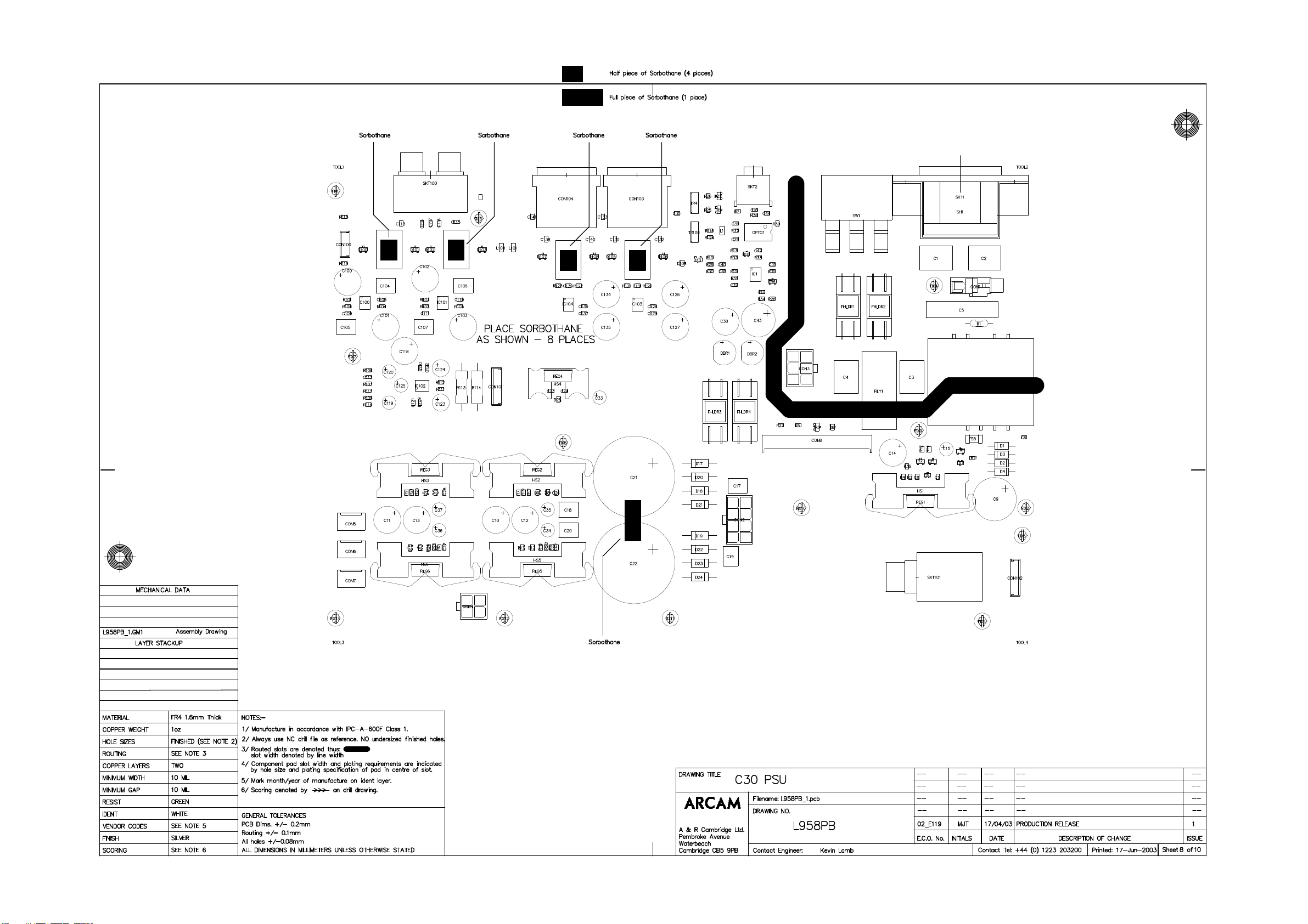
Page 44

C30 Preamplifier PSU/main cct board L958AY issue 2.0
Designator Part Description
C1 2K233 Capacitor X1 Y2 Rated Ceramic 7.5mm Pitch 3N3 250V
C2 2K233 Capacitor X1 Y2 Rated Ceramic 7.5mm Pitch 3N3 250V
C3 2K233 Capacitor X1 Y2 Rated Ceramic 7.5mm Pitch 3N3 250V
C4 2K233 Capacitor X1 Y2 Rated Ceramic 7.5mm Pitch 3N3 250V
C5 2D422 Capacitor X2 Boxed Polypropylene 22.5mm Pitch 275V 220NF
C6 2J410 Capacitor SM 0805 X7R Ceramic 10% 50V 100N
C7 2J410 Capacitor SM 0805 X7R Ceramic 10% 50V 100N
C8 2J410 Capacitor SM 0805 X7R Ceramic 10% 50V 100N
C9 2N833 Capacitor Radial Electrolytic Dia 16mm Pitch 7.5mm 3300UF 25V
C10 2P710A Capacitor Radial Electrolytic Oscon SA 100UF 20V
C11 2P710A Capacitor Radial Electrolytic Oscon SA 100UF 20V
C12 2P710A Capacitor Radial Electrolytic Oscon SA 100UF 20V
C13 2P710A Capacitor Radial Electrolytic Oscon SA 100UF 20V
C14 2N810A Capacitor Radial Electrolytic Dia 10mm Pitch 5mm 1000UF 10V
C15 2N610 Capacitor Radial Electrolytic Dia 5mm Pitch 5mm 10UF 50V
C16 2J410 Capacitor SM 0805 X7R Ceramic 10% 50V 100N
C17 2KA447 Capacitor Boxed Polyester 5mm Pitch 5% 100VDC 470N
C18 2KA447 Capacitor Boxed Polyester 5mm Pitch 5% 100VDC 470N
C19 2KA447 Capacitor Boxed Polyester 5mm Pitch 5% 100VDC 470N
C20 2KA447 Capacitor Boxed Polyester 5mm Pitch 5% 100VDC 470N
C21 2N910 Capacitor Radial Electrolytic Dia 30mm Claw Mount 10,000UF 50V
C22 2N910 Capacitor Radial Electrolytic Dia 30mm Claw Mount 10,000UF 50V
C23 2J410 Capacitor SM 0805 X7R Ceramic 10% 50V 100N
C24 2J410 Capacitor SM 0805 X7R Ceramic 10% 50V 100N
C25 2J410 Capacitor SM 0805 X7R Ceramic 10% 50V 100N
C26 2J410 Capacitor SM 0805 X7R Ceramic 10% 50V 100N
C27 2J410 Capacitor SM 0805 X7R Ceramic 10% 50V 100N
C28 2J410 Capacitor SM 0805 X7R Ceramic 10% 50V 100N
C29 2J410 Capacitor SM 0805 X7R Ceramic 10% 50V 100N
C30 2J410 Capacitor SM 0805 X7R Ceramic 10% 50V 100N
C31 2J410 Capacitor SM 0805 X7R Ceramic 10% 50V 100N
C32 2J410 Capacitor SM 0805 X7R Ceramic 10% 50V 100N
C33 2N710 Capacitor Radial Electrolytic Dia 5mm Pitch 5mm 100UF 25V
C34 2P622P Capacitor Radial Electrolytic Oscon SP 22UF 20V
C35 2P622P Capacitor Radial Electrolytic Oscon SP 22UF 20V
C36 2P622P Capacitor Radial Electrolytic Oscon SP 22UF 20V
C37 2P622P Capacitor Radial Electrolytic Oscon SP 22UF 20V
C38 2N710B Capacitor Radial Electrolytic Dia 10mm Pitch 5mm 100UF 100V
C39 2L110 Capacitor SM 0805 NPO Ceramic 5% 100V 100P
C40 2L115 Capacitor SM 0805 NPO Ceramic 5% 100V 150P
C41 2L115 Capacitor SM 0805 NPO Ceramic 5% 100V 150P
C42 2L168 Capacitor SM 0805 NPO Ceramic 5% 100V 680P
C43 2N810C Capacitor Radial Electrolytic Dia 12.5mm Pitch 5mm 1000UF 35V
C44 2J410 Capacitor SM 0805 X7R Ceramic 10% 50V 100N
C100 2P710AC Capacitor Radial Electrolytic Elna ROA Series 100UF 25V
C101 2P710AC Capacitor Radial Electrolytic Elna ROA Series 100UF 25V
C102 2P710AC Capacitor Radial Electrolytic Elna ROA Series 100UF 25V
C103 2P710AC Capacitor Radial Electrolytic Elna ROA Series 100UF 25V
C104 2KA310 Capacitor Boxed Polyester 5mm Pitch 5% 100VDC 10N
C105 2KA310 Capacitor Boxed Polyester 5mm Pitch 5% 100VDC 10N
C106 2KA310 Capacitor Boxed Polyester 5mm Pitch 5% 100VDC 10N
C107 2KA310 Capacitor Boxed Polyester 5mm Pitch 5% 100VDC 10N
C108 2L147 Capacitor SM 0805 NPO Ceramic 5% 100V 470P
C109 2L147 Capacitor SM 0805 NPO Ceramic 5% 100V 470P
C110 2L147 Capacitor SM 0805 NPO Ceramic 5% 100V 470P
C111 2L147 Capacitor SM 0805 NPO Ceramic 5% 100V 470P
C112 2J410 Capacitor SM 0805 X7R Ceramic 10% 50V 100N
C113 2L110 Capacitor SM 0805 NPO Ceramic 5% 100V 100P
C114 2L110 Capacitor SM 0805 NPO Ceramic 5% 100V 100P
C115 2L110 Capacitor SM 0805 NPO Ceramic 5% 100V 100P
C116 2L110 Capacitor SM 0805 NPO Ceramic 5% 100V 100P
Page 45

C30 Preamplifier PSU/main cct board L958AY issue 2.0
Designator Part Description
C117 2JA310 Capacitor SM 0805 X7R Ceramic 10% 100V 10N
C118 2N747 Capacitor Radial Electrolytic Dia 10mm Pitch 5mm 470UF 25V
C119 2N510 Capacitor Radial Electrolytic Dia 5mm Pitch 5mm 1UF 50V
C120 2N510 Capacitor Radial Electrolytic Dia 5mm Pitch 5mm 1UF 50V
C121 2L033 Capacitor SM 0805 NPO Ceramic 5% 100V 33P
C122 2L033 Capacitor SM 0805 NPO Ceramic 5% 100V 33P
C123 2N722 Capacitor Radial Electrolytic Dia 6.3mm Pitch 5mm 220UF 16V
C124 2N722 Capacitor Radial Electrolytic Dia 6.3mm Pitch 5mm 220UF 16V
C125 2N610 Capacitor Radial Electrolytic Dia 5mm Pitch 5mm 10UF 50V
C126 2P710AC Capacitor Radial Electrolytic Elna ROA Series 100UF 25V
C127 2P710AC Capacitor Radial Electrolytic Elna ROA Series 100UF 25V
C128 2J410 Capacitor SM 0805 X7R Ceramic 10% 50V 100N
C129 2J410 Capacitor SM 0805 X7R Ceramic 10% 50V 100N
C130 2L110 Capacitor SM 0805 NPO Ceramic 5% 100V 100P
C131 2L110 Capacitor SM 0805 NPO Ceramic 5% 100V 100P
C132 2L110 Capacitor SM 0805 NPO Ceramic 5% 100V 100P
C133 2JA310 Capacitor SM 0805 X7R Ceramic 10% 100V 10N
C134 2P710AC Capacitor Radial Electrolytic Elna ROA Series 100UF 25V
C135 2P710AC Capacitor Radial Electrolytic Elna ROA Series 100UF 25V
C136 2J410 Capacitor SM 0805 X7R Ceramic 10% 50V 100N
C137 2J410 Capacitor SM 0805 X7R Ceramic 10% 50V 100N
C138 2L110 Capacitor SM 0805 NPO Ceramic 5% 100V 100P
C139 2L110 Capacitor SM 0805 NPO Ceramic 5% 100V 100P
C140 2L110 Capacitor SM 0805 NPO Ceramic 5% 100V 100P
C141 2JA310 Capacitor SM 0805 X7R Ceramic 10% 100V 10N
CON1 8Q003 Con Cage Clamp 1WAY
CON2 8K2308 Con Minifit HCS 8WAY
CON3 8K2306 Con Minifit HCS 6WAY
CON4 8K2304 Con Minifit HCS 4WAY
CON5 8K6604 Con KK Series 0.1in Vertical Friction Lock Hdr 4WAY
CON6 8K6604 Con KK Series 0.1in Vertical Friction Lock Hdr 4WAY
CON7 8K6604 Con KK Series 0.1in Vertical Friction Lock Hdr 4WAY
CON8 8K7014 Con 2.54MM Vertical FFC 14WAY
CON100 8K2404 Con CT Series Vertical 4WAY
CON101 8K2406 Con CT Series Vertical 6WAY
CON102 8K2406 Con CT Series Vertical 6WAY
CON103 8K3101 XLR PCB Male Neutr k NC3MBH-B
CON104 8K3101 XLR PCB Male Neutr k NC3MBH-B
D1 3F5819 Diode Schottky 1N5819 DO-41 Package
D2 3F5819 Diode Schottky 1N5819 DO-41 Package
D3 3F5819 Diode Schottky 1N5819 DO-41 Package
D4 3F5819 Diode Schottky 1N5819 DO-41 Package
D5 3AS16W Diode Surface Mount Small Signal BAS16W SOT-23 Package
D6 3AS16W Diode Surface Mount Small Signal BAS16W SOT-23 Package
D7 3AS16W Diode Surface Mount Small Signal BAS16W SOT-23 Package
D8 3AS16W Diode Surface Mount Small Signal BAS16W SOT-23 Package
D9 3AS16W Diode Surface Mount Small Signal BAS16W SOT-23 Package
D10 3AS16W Diode Surface Mount Small Signal BAS16W SOT-23 Package
D11 3AS16W Diode Surface Mount Small Signal BAS16W SOT-23 Package
D12 3AS16W Diode Surface Mount Small Signal BAS16W SOT-23 Package
D13 3AS16W Diode Surface Mount Small Signal BAS16W SOT-23 Package
D14 3AS16W Diode Surface Mount Small Signal BAS16W SOT-23 Package
D15 3AS16W Diode Surface Mount Small Signal BAS16W SOT-23 Package
D16 3AS16W Diode Surface Mount Small Signal BAS16W SOT-23 Package
D17 3BYV27 Diode SBYV27-200 DO-15 Package
D18 3BYV27 Diode SBYV27-200 DO-15 Package
D19 3BYV27 Diode SBYV27-200 DO-15 Package
D20 3BYV27 Diode SBYV27-200 DO-15 Package
D21 3BYV27 Diode SBYV27-200 DO-15 Package
D22 3BYV27 Diode SBYV27-200 DO-15 Package
D23 3BYV27 Diode SBYV27-200 DO-15 Package
Page 46

C30 Preamplifier PSU/main cct board L958AY issue 2.0
Designator Part Description
D24 3BYV27 Diode SBYV27-200 DO-15 Package
D25 3AS16W Diode Surface Mount Small Signal BAS16W SOT-23 Package
D100 3AV99W Diode Dual Surface Mount Small Signal BAV99 SOT-23 Package
D101 3AV99W Diode Dual Surface Mount Small Signal BAV99 SOT-23 Package
D102 3AV99W Diode Dual Surface Mount Small Signal BAV99 SOT-23 Package
D103 3AV99W Diode Dual Surface Mount Small Signal BAV99 SOT-23 Package
D104 3AS16W Diode Surface Mount Small Signal BAS16W SOT-23 Package
D105 3AV99W Diode Dual Surface Mount Small Signal BAV99 SOT-23 Package
D106 3AV99W Diode Dual Surface Mount Small Signal BAV99 SOT-23 Package
D107 3AV99W Diode Dual Surface Mount Small Signal BAV99 SOT-23 Package
D108 3AV99W Diode Dual Surface Mount Small Signal BAV99 SOT-23 Package
DBR1 3BW02 Diode Bridge Rectifier W02G Plastic Package
DBR2 3BW02 Diode Bridge Rectifier W02G Plastic Package
DZ1 3CW32V7 Zener Diode 0.25W Surface Mount BZX84C2V7 SOT-23 Package
DZ2 3CW315V Zener Diode 0.25W Surface Mount BZX84C15V SOT-23 Package
DZ3 3CW33V9 Zener Diode 0.25W Surface Mount BZX84C3V9 SOT-23 Package
FHLDR1 8S004 Fuseholder 20MM PCB
FHLDR2 8S004 Fuseholder 20MM PCB
FHLDR3 8S004 Fuseholder 20MM PCB
FHLDR4 8S004 Fuseholder 20MM PCB
FS3 C54125 Fuse Bussmann S504 T250mA
FS4 C54125 Fuse Bussmann S504 T250mA
FS5 C3501 Fuse Littelfuse T500mA SM
HS1 F008 Heatsink TO-220 SW50-2 8.8 Deg C/W
HS2 F008 Heatsink TO-220 SW50-2 8.8 Deg C/W
HS3 F008 Heatsink TO-220 SW50-2 8.8 Deg C/W
HS4 F004 Heatsink TO-220 PF752 23.7 Degc/W
HS5 F008 Heatsink TO-220 SW50-2 8.8 Deg C/W
HS6 F008 Heatsink TO-220 SW50-2 8.8 Deg C/W
IC1 5B972 Opamp TS972ID SO-8 Package
IC100 5B797 Opamp AD797AR SO-8 Package
IC101 5B797 Opamp AD797AR SO-8 Package
IC102 5A4880 IC Headphone Amp Nat Semi LM4880M SO-8 Package
IC103 5B135 IC Balanced Driver Burr-Brown DRV135UA SO-8 Package
IC104 5B135 IC Balanced Driver Burr-Brown DRV135UA SO-8 Package
ITEM1-1 L958PB Blank PCB C30 Preamp PSU
ITEM2-1 F006 Clip For SW Profile Heatsink
ITEM3-1 F006 Clip For SW Profile Heatsink
ITEM4-1 F006 Clip For SW Profile Heatsink
ITEM6-1 F006 Clip For SW Profile Heatsink
ITEM7-1 F006 Clip For SW Profile Heatsink
ITEM8-1 E802AP Pad Damping 15x6x3MM Sorbothane
ITEM9-1 E826AP Pad Damping 7.5x6x3 Sorbothane
ITEM10-1 E826AP Pad Damping 7.5x6x3 Sorbothane
ITEM11-1 E826AP Pad Damping 7.5x6x3 Sorbothane
ITEM12-1 E826AP Pad Damping 7.5x6x3 Sorbothane
ITEM13-1 F022 Fuseholder Cover For 20mm Fuseholder
ITEM14-1 F022 Fuseholder Cover For 20mm Fuseholder
ITEM15-1 F022 Fuseholder Cover For 20mm Fuseholder
ITEM16-1 F022 Fuseholder Cover For 20mm Fuseholder
ITEM17-1 8M101 Earth Lead Assy 75MM
L1 7F004 Ferrite Bead SM1206 70R@100MHz
L100 7F004 Ferrite Bead SM1206 70R@100MHz
L101 7F004 Ferrite Bead SM1206 70R@100MHz
OPTO1 5T4N35 Opto Isolator 4N35
R1 1KA515 Resistor Metal Glazed 0.5W 5% 1M5
R2 1M000 Resistor 0805 Surface Mount 0.125W 1% 0R0
R3 1M127 Resistor 0805 Surface Mount 0.125W 1% 270R
R4 1M168 Resistor 0805 Surface Mount 0.125W 1% 680R
R5 1M222 Resistor 0805 Surface Mount 0.125W 1% 2K2
R6 1M222 Resistor 0805 Surface Mount 0.125W 1% 2K2
Page 47

C30 Preamplifier PSU/main cct board L958AY issue 2.0
Designator Part Description
R7 1M222 Resistor 0805 Surface Mount 0.125W 1% 2K2
R8 1M222 Resistor 0805 Surface Mount 0.125W 1% 2K2
R9 1M222 Resistor 0805 Surface Mount 0.125W 1% 2K2
R10 1M222 Resistor 0805 Surface Mount 0.125W 1% 2K2
R11 1M310 Resistor 0805 Surface Mount 0.125W 1% 10K
R12 1M310 Resistor 0805 Surface Mount 0.125W 1% 10K
R13 1M310 Resistor 0805 Surface Mount 0.125W 1% 10K
R14 1M233 Resistor 0805 Surface Mount 0.125W 1% 3K3
R15 1M233 Resistor 0805 Surface Mount 0.125W 1% 3K3
R16 1M233 Resistor 0805 Surface Mount 0.125W 1% 3K3
R17 1M068 Resistor 0805 Surface Mount 0.125W 1% 68R
R18 1M068 Resistor 0805 Surface Mount 0.125W 1% 68R
R19 1M110 Resistor 0805 Surface Mount 0.125W 1% 100R
R20 1M110 Resistor 0805 Surface Mount 0.125W 1% 100R
R21 1M110 Resistor 0805 Surface Mount 0.125W 1% 100R
R22 1M110 Resistor 0805 Surface Mount 0.125W 1% 100R
R23 1M110 Resistor 0805 Surface Mount 0.125W 1% 100R
R24 1M110 Resistor 0805 Surface Mount 0.125W 1% 100R
R25 1M010 Resistor 0805 Surface Mount 0.125W 1% 10R
R26 1M233 Resistor 0805 Surface Mount 0.125W 1% 3K3
R27 1M010 Resistor 0805 Surface Mount 0.125W 1% 10R
R28 1M322 Resistor 0805 Surface Mount 0.125W 1% 22K
R29 1M427 Resistor 0805 Surface Mount 0.125W 1% 270K
R30 1M212 Resistor 0805 Surface Mount 0.125W 1% 1K2
R31 1M218 Resistor 0805 Surface Mount 0.125W 1% 1K8
R32 1M468 Resistor 0805 Surface Mount 0.125W 1% 680K
R33 1M447 Resistor 0805 Surface Mount 0.125W 1% 470K
R34 1M215 Resistor 0805 Surface Mount 0.125W 1% 1K5
R35 1M247 Resistor 0805 Surface Mount 0.125W 1% 4K7
R36 1M268 Resistor 0805 Surface Mount 0.125W 1% 6K8
R37 1M000 Resistor 0805 Surface Mount 0.125W 1% 0R0
R38 1M000 Resistor 0805 Surface Mount 0.125W 1% 0R0
R39 1M147 Resistor 0805 Surface Mount 0.125W 1% 470R
R100 1M110 Resistor 0805 Surface Mount 0.125W 1% 100R
R101 1M110 Resistor 0805 Surface Mount 0.125W 1% 100R
R102 1M110 Resistor 0805 Surface Mount 0.125W 1% 100R
R103 1M110 Resistor 0805 Surface Mount 0.125W 1% 100R
R104 1M047 Resistor 0805 Surface Mount 0.125W 1% 47R
R105 1M047 Resistor 0805 Surface Mount 0.125W 1% 47R
R106 1M315 Resistor 0805 Surface Mount 0.125W 1% 15K
R107 1M315 Resistor 0805 Surface Mount 0.125W 1% 15K
R108 1M822 Resistor 0805 Surface Mount 0.125W 1% 2R2
R109 1M310 Resistor 0805 Surface Mount 0.125W 1% 10K
R110 1M310 Resistor 0805 Surface Mount 0.125W 1% 10K
R111 1M347 Resistor 0805 Surface Mount 0.125W 1% 47K
R112 1M347 Resistor 0805 Surface Mount 0.125W 1% 47K
R113 1E847 Resistor Carbon Film 1W 5% 4R7
R114 1E847 Resistor Carbon Film 1W 5% 4R7
R115 1M115 Resistor 0805 Surface Mount 0.125W 1% 150R
R116 1M410 Resistor 0805 Surface Mount 0.125W 1% 100K
R117 1M410 Resistor 0805 Surface Mount 0.125W 1% 100K
R118 1M310 Resistor 0805 Surface Mount 0.125W 1% 10K
R119 1M310 Resistor 0805 Surface Mount 0.125W 1% 10K
R120 1M047 Resistor 0805 Surface Mount 0.125W 1% 47R
R121 1M047 Resistor 0805 Surface Mount 0.125W 1% 47R
R122 1M047 Resistor 0805 Surface Mount 0.125W 1% 47R
R123 1M047 Resistor 0805 Surface Mount 0.125W 1% 47R
R124 1M115 Resistor 0805 Surface Mount 0.125W 1% 150R
R125 1M010 Resistor 0805 Surface Mount 0.125W 1% 10R
R1000 1H210 Resistor Metal Film 0.25W 1% 1K0
REG4 5D7805 IC Voltage Regulator +5V L7805CV TO-220 Package
Page 48

C30 Preamplifier PSU/main cct board L958AY issue 2.0
Designator Part Description
REG3 5D317T IC Voltage Regulator ADJ LM317T TO-220 Package
REG2 5D317T IC Voltage Regulator ADJ LM317T TO-220 Package
REG5 5D337 IC Voltage Regulator Neg ADJ LM337T TO-220 Package
REG6 5D337 IC Voltage Regulator Neg ADJ LM337T TO-220 Package
REG1 5D1086A IC Voltage Regulator ADJ LM1086CT-ADJ TO-220 Package
RLY1 A219 Relay 2P2T 5V
RLY100 A215 Relay 2P2T 12V SM
RLY101 A215 Relay 2P2T 12V SM
RLY102 A215 Relay 2P2T 12V SM
RLY103 A215 Relay 2P2T 12V SM
SH1 E5402 Shield EMC IEC Inlet Mains
SKT1 8A001 Mains IEC Inlet 3PIN PCB Ins
SKT2 8D302 Con Jack 3.5mm Dual Mono
SKT100 8D225 Phono Skt 4-WAY Gold
SKT101 8D301 Con Jack 6mm Stereo
SW1 A1404 Switch Slide Volt Sel
TX1 7A9301 Transformer PCB mount 9V+9V 3VA 115/230V
TX1 L907TX Transformer PCB mount 9V+9V 3VA 100V
TR1 4A849B Transistor BC849B SOT23 Package
TR2 4A849B Transistor BC849B SOT23 Package
TR3 4AFMMT497 Transistor FMMT497 SOT23 Package
TR4 4B179 Transistor BD179 TO126 Package
TR5 4AFMMT497 Transistor FMMT497 SOT23 Package
TR6 4D10KN Digital Transistor MMUN2211LT1 SOT23 Package
TR100 4B179 Transistor BD179 TO126 Package
Page 49

Page 50

C30 Preamplifier pre-amp cct board L965AY issue 1.2
Designator Part Description
C100 2C210 Capacitor SM 1206 NPO Ceramic 50V 5% 1N0
C101 2DA147 Capacitor Boxed Polypropylene 5mm Pitch 100V 5% 470P
C102 2DA147 Capacitor Boxed Polypropylene 5mm Pitch 100V 5% 470P
C103 2DA147 Capacitor Boxed Polypropylene 5mm Pitch 100V 5% 470P
C104 2C410 Capacitor SM 1206 X7R Ceramic 50V 10% 100N
C105 2C410 Capacitor SM 1206 X7R Ceramic 50V 10% 100N
C106 2C410 Capacitor SM 1206 X7R Ceramic 50V 10% 100N
C107 2C410 Capacitor SM 1206 X7R Ceramic 50V 10% 100N
C108 2C110 Capacitor SM 1206 NPO Ceramic 50V 5% 100PF
C109 2C110 Capacitor SM 1206 NPO Ceramic 50V 5% 100PF
C110 2N710 Capacitor Radial Electrolytic Dia 5mm Pitch 5mm 100UF 25V
C111 2P610CC Capacitor Radial Electrolytic Elna ROA 10UF 50V
C112 2K447 Capacitor Boxed Polyester 5mm Pitch 10% 63V 470N
C113 2K447 Capacitor Boxed Polyester 5mm Pitch 10% 63V 470N
C114 2D222W Capacitor Boxed Polyprop 5mm Pitch 100V 5% 2N2
C115 2C022 Capacitor SM 1206 NPO Ceramic 100V 5% 22PF
C116 2P610CC Capacitor Radial Electrolytic Elna ROA 10UF 50V
C117 2P610CC Capacitor Radial Electrolytic Elna ROA 10UF 50V
C118 2C410 Capacitor SM 1206 X7R Ceramic 50V 10% 100N
C119 2C310 Capacitor SM 1206 X7R Ceramic 50V 10% 10NF
C120 2N610 Capacitor Radial Electrolytic Dia 5mm Pitch 5mm 10UF 50V
C121 2C210 Capacitor SM 1206 NPO Ceramic 50V 5% 1N0
C122 2DA147 Capacitor Boxed Polypropylene 5mm Pitch 100V 5% 470P
C123 2DA147 Capacitor Boxed Polypropylene 5mm Pitch 100V 5% 470P
C124 2DA147 Capacitor Boxed Polypropylene 5mm Pitch 100V 5% 470P
C125 2C410 Capacitor SM 1206 X7R Ceramic 50V 10% 100N
C126 2C410 Capacitor SM 1206 X7R Ceramic 50V 10% 100N
C127 2C410 Capacitor SM 1206 X7R Ceramic 50V 10% 100N
C128 2C410 Capacitor SM 1206 X7R Ceramic 50V 10% 100N
C129 2C110 Capacitor SM 1206 NPO Ceramic 50V 5% 100PF
C130 2C110 Capacitor SM 1206 NPO Ceramic 50V 5% 100PF
C131 2N710 Capacitor Radial Electrolytic Dia 5mm Pitch 5mm 100UF 25V
C132 2P610CC Capacitor Radial Electrolytic Elna ROA 10UF 50V
C133 2K447 Capacitor Boxed Polyester 5mm Pitch 10% 63V 470N
C134 2K447 Capacitor Boxed Polyester 5mm Pitch 10% 63V 470N
C135 2D222W Capacitor Boxed Polyprop 5mm Pitch 100V 5% 2N2
C136 2C022 Capacitor SM 1206 NPO Ceramic 100V 5% 22PF
C137 2P610CC Capacitor Radial Electrolytic Elna ROA 10UF 50V
C138 2P610CC Capacitor Radial Electrolytic Elna ROA 10UF 50V
C139 2C210 Capacitor SM 1206 NPO Ceramic 50V 5% 1N0
C140 2DA147 Capacitor Boxed Polypropylene 5mm Pitch 100V 5% 470P
C141 2DA147 Capacitor Boxed Polypropylene 5mm Pitch 100V 5% 470P
C142 2DA147 Capacitor Boxed Polypropylene 5mm Pitch 100V 5% 470P
C143 2C410 Capacitor SM 1206 X7R Ceramic 50V 10% 100N
C144 2C410 Capacitor SM 1206 X7R Ceramic 50V 10% 100N
C145 2C410 Capacitor SM 1206 X7R Ceramic 50V 10% 100N
C146 2C410 Capacitor SM 1206 X7R Ceramic 50V 10% 100N
C147 2KA410 Capacitor Boxed Polyester 5mm Pitch 5% 100VDC 100N
C148 2C022 Capacitor SM 1206 NPO Ceramic 100V 5% 22PF
C149 2C022 Capacitor SM 1206 NPO Ceramic 100V 5% 22PF
C150 2K447 Capacitor Boxed Polyester 5mm Pitch 10% 63V 470N
C151 2K447 Capacitor Boxed Polyester 5mm Pitch 10% 63V 470N
C152 2C410 Capacitor SM 1206 X7R Ceramic 50V 10% 100N
C153 2C410 Capacitor SM 1206 X7R Ceramic 50V 10% 100N
C154 2P622P Capacitor Radial Electrolytic Oscon SP 22UF 20V
C155 2C410 Capacitor SM 1206 X7R Ceramic 50V 10% 100N
C156 2C410 Capacitor SM 1206 X7R Ceramic 50V 10% 100N
C157 2P622P Capacitor Radial Electrolytic Oscon SP 22UF 20V
C158 2C022 Capacitor SM 1206 NPO Ceramic 100V 5% 22PF
C159 2C022 Capacitor SM 1206 NPO Ceramic 100V 5% 22PF
C160 2C210 Capacitor SM 1206 NPO Ceramic 50V 5% 1N0
Page 51

C30 Preamplifier pre-amp cct board L965AY issue 1.2
Designator Part Description
C161 2DA147 Capacitor Boxed Polypropylene 5mm Pitch 100V 5% 470P
C162 2DA147 Capacitor Boxed Polypropylene 5mm Pitch 100V 5% 470P
C163 2DA147 Capacitor Boxed Polypropylene 5mm Pitch 100V 5% 470P
C164 2C210 Capacitor SM 1206 NPO Ceramic 50V 5% 1N0
C165 2DA147 Capacitor Boxed Polypropylene 5mm Pitch 100V 5% 470P
C166 2DA147 Capacitor Boxed Polypropylene 5mm Pitch 100V 5% 470P
C167 2KA410 Capacitor Boxed Polyester 5mm Pitch 5% 100VDC 100N
C168 2C410 Capacitor SM 1206 X7R Ceramic 50V 10% 100N
C169 2C410 Capacitor SM 1206 X7R Ceramic 50V 10% 100N
C170 2C410 Capacitor SM 1206 X7R Ceramic 50V 10% 100N
C171 2C410 Capacitor SM 1206 X7R Ceramic 50V 10% 100N
C172 2C410 Capacitor SM 1206 X7R Ceramic 50V 10% 100N
C173 2C410 Capacitor SM 1206 X7R Ceramic 50V 10% 100N
C174 2C410 Capacitor SM 1206 X7R Ceramic 50V 10% 100N
C175 2C410 Capacitor SM 1206 X7R Ceramic 50V 10% 100N
C176 2C410 Capacitor SM 1206 X7R Ceramic 50V 10% 100N
C177 2C410 Capacitor SM 1206 X7R Ceramic 50V 10% 100N
C178 2C410 Capacitor SM 1206 X7R Ceramic 50V 10% 100N
C179 2C410 Capacitor SM 1206 X7R Ceramic 50V 10% 100N
C180 2C410 Capacitor SM 1206 X7R Ceramic 50V 10% 100N
C181 2C410 Capacitor SM 1206 X7R Ceramic 50V 10% 100N
C182 2C410 Capacitor SM 1206 X7R Ceramic 50V 10% 100N
C183 2C410 Capacitor SM 1206 X7R Ceramic 50V 10% 100N
C184 2C410 Capacitor SM 1206 X7R Ceramic 50V 10% 100N
C185 2C410 Capacitor SM 1206 X7R Ceramic 50V 10% 100N
C186 2C410 Capacitor SM 1206 X7R Ceramic 50V 10% 100N
C187 2N610 Capacitor Radial Electrolytic Dia 5mm Pitch 5mm 10UF 50V
C188 2P622P Capacitor Radial Electrolytic Oscon SP 22UF 20V
C189 2P622P Capacitor Radial Electrolytic Oscon SP 22UF 20V
C190 2P622P Capacitor Radial Electrolytic Oscon SP 22UF 20V
C191 2P622P Capacitor Radial Electrolytic Oscon SP 22UF 20V
C192 2K447 Capacitor Boxed Polyester 5mm Pitch 10% 63V 470N
C193 2K447 Capacitor Boxed Polyester 5mm Pitch 10% 63V 470N
C300 2N810C Capacitor Radial Electrolytic Dia 12.5mm Pitch 5mm 1000UF 35V
C302 2P622P Capacitor Radial Electrolytic Oscon SP 22UF 20V
C303 2P710A Capacitor Radial Electrolytic Oscon SA 100UF 20V
C304 2C410 Capacitor SM 1206 X7R Ceramic 50V 10% 100N
C305 2KA410 Capacitor Boxed Polyester 5mm Pitch 5% 100VDC 100N
C306 2P710A Capacitor Radial Electrolytic Oscon SA 100UF 20V
C307 2K447 Capacitor Boxed Polyester 5mm Pitch 10% 63V 470N
C308 2C410 Capacitor SM 1206 X7R Ceramic 50V 10% 100N
C309 2C410 Capacitor SM 1206 X7R Ceramic 50V 10% 100N
C310 2N810C Capacitor Radial Electrolytic Dia 12.5mm Pitch 5mm 1000UF 35V
C312 2P622P Capacitor Radial Electrolytic Oscon SP 22UF 20V
C313 2P710A Capacitor Radial Electrolytic Oscon SA 100UF 20V
C314 2KA410 Capacitor Boxed Polyester 5mm Pitch 5% 100VDC 100N
C315 2KA410 Capacitor Boxed Polyester 5mm Pitch 5% 100VDC 100N
D100 3AV99W Diode Dual Surface Mount Small Signal BAV99 SOT-23 Package
D101 3AV99W Diode Dual Surface Mount Small Signal BAV99 SOT-23 Package
D102 3AV99W Diode Dual Surface Mount Small Signal BAV99 SOT-23 Package
D103 3AV99W Diode Dual Surface Mount Small Signal BAV99 SOT-23 Package
D104 3AV99W Diode Dual Surface Mount Small Signal BAV99 SOT-23 Package
D105 3AV99W Diode Dual Surface Mount Small Signal BAV99 SOT-23 Package
D106 3AV99W Diode Dual Surface Mount Small Signal BAV99 SOT-23 Package
D107 3AV99W Diode Dual Surface Mount Small Signal BAV99 SOT-23 Package
D108 3AV99W Diode Dual Surface Mount Small Signal BAV99 SOT-23 Package
D109 3AV99W Diode Dual Surface Mount Small Signal BAV99 SOT-23 Package
D110 3AV99W Diode Dual Surface Mount Small Signal BAV99 SOT-23 Package
D111 3AV99W Diode Dual Surface Mount Small Signal BAV99 SOT-23 Package
D112 3AV99W Diode Dual Surface Mount Small Signal BAV99 SOT-23 Package
D113 3AV99W Diode Dual Surface Mount Small Signal BAV99 SOT-23 Package
Page 52

C30 Preamplifier pre-amp cct board L965AY issue 1.2
Designator Part Description
D114 3AV99W Diode Dual Surface Mount Small Signal BAV99 SOT-23 Package
D115 3AV99W Diode Dual Surface Mount Small Signal BAV99 SOT-23 Package
D116 3AV99W Diode Dual Surface Mount Small Signal BAV99 SOT-23 Package
D117 3AV99W Diode Dual Surface Mount Small Signal BAV99 SOT-23 Package
D118 3AV99W Diode Dual Surface Mount Small Signal BAV99 SOT-23 Package
D119 3AV99W Diode Dual Surface Mount Small Signal BAV99 SOT-23 Package
D120 3AS16W Diode Surface Mount Small Signal BAS16W SOT-23 Package
D121 3AV99W Diode Dual Surface Mount Small Signal BAV99 SOT-23 Package
D122 3AV99W Diode Dual Surface Mount Small Signal BAV99 SOT-23 Package
D300 3BS1D Diode Surface Mount S1D
D301 3BS1D Diode Surface Mount S1D
D302 3AS16W Diode Surface Mount Small Signal BAS16W SOT-23 Package
D304 3AS16W Diode Surface Mount Small Signal BAS16W SOT-23 Package
D305 3AS16W Diode Surface Mount Small Signal BAS16W SOT-23 Package
D306 3BS1D Diode Surface Mount S1D
D307 3BS1D Diode Surface Mount S1D
D308 3AS16W Diode Surface Mount Small Signal BAS16W SOT-23 Package
D310 3CW315V Zener Diode 0.25W Surface Mount BZX84C15V SOT-23 Package
D311 3CW315V Zener Diode 0.25W Surface Mount BZX84C15V SOT-23 Package
F300 C3202 Fuse Littelfuse T2A SM
F301 C3202 Fuse Littelfuse T2A SM
ITEM1-1 E826AP Pad Damping 7.5x6x3 Sorbothane
ITEM2-1 E826AP Pad Damping 7.5x6x3 Sorbothane
PCB1 L937PB Blank PCB A32 Preamp PCB
Q100 4A849B Transistor BC849B SOT23 Package
Q300 4J112 Transistor Jfet N Channel J112 TO-92 Package
Q301 4B5171 Transistor 2SC5171 TO220 Package
Q303 4J112 Transistor Jfet N Channel J112 TO-92 Package
Q305 4B1930 Transistor 2SA1930 TO220 Package
Q306 4A846B Transistor BC846B SOT23 Package
Q307 4A856B Transistor BC856B SOT23 Package
R100 1A210 Resistor 1206 Surface Mount 0.25W 1% 1K0
R101 1A210 Resistor 1206 Surface Mount 0.25W 1% 1K0
R102 1A210 Resistor 1206 Surface Mount 0.25W 1% 1K0
R103 1A410 Resistor 1206 Surface Mount 0.25W 1% 100K
R104 1A410 Resistor 1206 Surface Mount 0.25W 1% 100K
R105 1A410 Resistor 1206 Surface Mount 0.25W 1% 100K
R106 1A510 Resistor 1206 Surface Mount 0.25W 1% 1M0
R107 1A510 Resistor 1206 Surface Mount 0.25W 1% 1M0
R108 1A047 Resistor 1206 Surface Mount 0.25W 1% 47R
R109 1A047 Resistor 1206 Surface Mount 0.25W 1% 47R
R110 1A222 Resistor 1206 Surface Mount 0.25W 1% 2K2
R111 1A222 Resistor 1206 Surface Mount 0.25W 1% 2K2
R112 1A322 Resistor 1206 Surface Mount 0.25W 1% 22K
R113 1A322 Resistor 1206 Surface Mount 0.25W 1% 22K
R114 1A322 Resistor 1206 Surface Mount 0.25W 1% 22K
R115 1A227 Resistor 1206 Surface Mount 0.25W 1% 2K7
R116 1A227 Resistor 1206 Surface Mount 0.25W 1% 2K7
R117 1A256 Resistor 1206 Surface Mount 0.25W 1% 5K6
R118 1A322 Resistor 1206 Surface Mount 0.25W 1% 22K
R119 1A322 Resistor 1206 Surface Mount 0.25W 1% 22K
R120 1A322 Resistor 1206 Surface Mount 0.25W 1% 22K
R121 1A322 Resistor 1206 Surface Mount 0.25W 1% 22K
R122 1A822 Resistor 1206 Surface Mount 0.25W 1% 2R2
R123 1A822 Resistor 1206 Surface Mount 0.25W 1% 2R2
R124 1A822 Resistor 1206 Surface Mount 0.25W 1% 2R2
R125 1A210 Resistor 1206 Surface Mount 0.25W 1% 1K0
R126 1A210 Resistor 1206 Surface Mount 0.25W 1% 1K0
R127 1A210 Resistor 1206 Surface Mount 0.25W 1% 1K0
R128 1A410 Resistor 1206 Surface Mount 0.25W 1% 100K
R129 1A410 Resistor 1206 Surface Mount 0.25W 1% 100K
Page 53

C30 Preamplifier pre-amp cct board L965AY issue 1.2
Designator Part Description
R130 1A410 Resistor 1206 Surface Mount 0.25W 1% 100K
R131 1A510 Resistor 1206 Surface Mount 0.25W 1% 1M0
R132 1A510 Resistor 1206 Surface Mount 0.25W 1% 1M0
R133 1A047 Resistor 1206 Surface Mount 0.25W 1% 47R
R134 1A047 Resistor 1206 Surface Mount 0.25W 1% 47R
R135 1A222 Resistor 1206 Surface Mount 0.25W 1% 2K2
R136 1A222 Resistor 1206 Surface Mount 0.25W 1% 2K2
R137 1A322 Resistor 1206 Surface Mount 0.25W 1% 22K
R138 1A322 Resistor 1206 Surface Mount 0.25W 1% 22K
R139 1A322 Resistor 1206 Surface Mount 0.25W 1% 22K
R140 1A227 Resistor 1206 Surface Mount 0.25W 1% 2K7
R141 1A227 Resistor 1206 Surface Mount 0.25W 1% 2K7
R142 1A256 Resistor 1206 Surface Mount 0.25W 1% 5K6
R143 1A322 Resistor 1206 Surface Mount 0.25W 1% 22K
R144 1A322 Resistor 1206 Surface Mount 0.25W 1% 22K
R145 1A322 Resistor 1206 Surface Mount 0.25W 1% 22K
R146 1A322 Resistor 1206 Surface Mount 0.25W 1% 22K
R147 1A322 Resistor 1206 Surface Mount 0.25W 1% 22K
R148 1A322 Resistor 1206 Surface Mount 0.25W 1% 22K
R149 1A322 Resistor 1206 Surface Mount 0.25W 1% 22K
R150 1A322 Resistor 1206 Surface Mount 0.25W 1% 22K
R151 1A322 Resistor 1206 Surface Mount 0.25W 1% 22K
R152 1A322 Resistor 1206 Surface Mount 0.25W 1% 22K
R153 1A322 Resistor 1206 Surface Mount 0.25W 1% 22K
R154 1A322 Resistor 1206 Surface Mount 0.25W 1% 22K
R155 1A322 Resistor 1206 Surface Mount 0.25W 1% 22K
R156 1A210 Resistor 1206 Surface Mount 0.25W 1% 1K0
R157 1A210 Resistor 1206 Surface Mount 0.25W 1% 1K0
R158 1A210 Resistor 1206 Surface Mount 0.25W 1% 1K0
R159 1A410 Resistor 1206 Surface Mount 0.25W 1% 100K
R160 1A410 Resistor 1206 Surface Mount 0.25W 1% 100K
R161 1A410 Resistor 1206 Surface Mount 0.25W 1% 100K
R162 1A322 Resistor 1206 Surface Mount 0.25W 1% 22K
R163 1A322 Resistor 1206 Surface Mount 0.25W 1% 22K
R164 1A322 Resistor 1206 Surface Mount 0.25W 1% 22K
R165 1A322 Resistor 1206 Surface Mount 0.25W 1% 22K
R166 1A322 Resistor 1206 Surface Mount 0.25W 1% 22K
R167 1A322 Resistor 1206 Surface Mount 0.25W 1% 22K
R168 1A322 Resistor 1206 Surface Mount 0.25W 1% 22K
R169 1A322 Resistor 1206 Surface Mount 0.25W 1% 22K
R170 1A322 Resistor 1206 Surface Mount 0.25W 1% 22K
R171 1A322 Resistor 1206 Surface Mount 0.25W 1% 22K
R172 1A322 Resistor 1206 Surface Mount 0.25W 1% 22K
R173 1A322 Resistor 1206 Surface Mount 0.25W 1% 22K
R174 1A322 Resistor 1206 Surface Mount 0.25W 1% 22K
R175 1A322 Resistor 1206 Surface Mount 0.25W 1% 22K
R176 1A322 Resistor 1206 Surface Mount 0.25W 1% 22K
R177 1A322 Resistor 1206 Surface Mount 0.25W 1% 22K
R178 1A322 Resistor 1206 Surface Mount 0.25W 1% 22K
R179 1A322 Resistor 1206 Surface Mount 0.25W 1% 22K
R180 1A410 Resistor 1206 Surface Mount 0.25W 1% 100K
R181 1A310 Resistor 1206 Surface Mount 0.25W 1% 10K
R182 1A110 Resistor 1206 Surface Mount 0.25W 1% 100R
R183 1A510 Resistor 1206 Surface Mount 0.25W 1% 1M0
R184 1A510 Resistor 1206 Surface Mount 0.25W 1% 1M0
R185 1A022 Resistor 1206 Surface Mount 0.25W 1% 22R
R186 1A047 Resistor 1206 Surface Mount 0.25W 1% 47R
R187 1A047 Resistor 1206 Surface Mount 0.25W 1% 47R
R188 1A310 Resistor 1206 Surface Mount 0.25W 1% 10K
R189 1A210 Resistor 1206 Surface Mount 0.25W 1% 1K0
R190 1A210 Resistor 1206 Surface Mount 0.25W 1% 1K0
Page 54

C30 Preamplifier pre-amp cct board L965AY issue 1.2
Designator Part Description
R191 1A210 Resistor 1206 Surface Mount 0.25W 1% 1K0
R192 1A410 Resistor 1206 Surface Mount 0.25W 1% 100K
R193 1A410 Resistor 1206 Surface Mount 0.25W 1% 100K
R194 1A410 Resistor 1206 Surface Mount 0.25W 1% 100K
R195 1A210 Resistor 1206 Surface Mount 0.25W 1% 1K0
R196 1A210 Resistor 1206 Surface Mount 0.25W 1% 1K0
R197 1A410 Resistor 1206 Surface Mount 0.25W 1% 100K
R198 1A410 Resistor 1206 Surface Mount 0.25W 1% 100K
R199 1A410 Resistor 1206 Surface Mount 0.25W 1% 100K
R200 1A822 Resistor 1206 Surface Mount 0.25W 1% 2R2
R201 1A822 Resistor 1206 Surface Mount 0.25W 1% 2R2
R202 1A822 Resistor 1206 Surface Mount 0.25W 1% 2R2
R203 1A247 Resistor 1206 Surface Mount 0.25W 1% 4K7
R204 1A310 Resistor 1206 Surface Mount 0.25W 1% 10K
R300 1A133 Resistor 1206 Surface Mount 0.25W 1% 330R
R302 1A212 Resistor 1206 Surface Mount 0.25W 1% 1K2
R303 1A147 Resistor 1206 Surface Mount 0.25W 1% 470R
R304 1A133 Resistor 1206 Surface Mount 0.25W 1% 330R
R307 1A122 Resistor 1206 Surface Mount 0.25W 1% 220R
RLY100 A216 Relay 2P2T 5V SM
SK2 8D225 Phono Skt 4-WAY Gold
SK3 8D225 Phono Skt 4-WAY Gold
SK4 8D225 Phono Skt 4-WAY Gold
SK5 8D225 Phono Skt 4-WAY Gold
SK6 8D226 Phono Skt 2-WAY Vert Gold
SK100 8K8022B Con 1.00MM Vertical FFC 22WAY 52806 Series
SK101 8K8330 Con 1.00MM Vertical SM FFC 30WAY
SK102 8K2404 Con CT Series Vertical 4WAY
SK103 8K2408 Con CT Series Vertical 8WAY
SK300 8K2304 Con Minifit HCS 4WAY
SK301 8K6604 Con KK Series 0.1in Vertical Friction Lock Hdr 4WAY
Z100 5S408DY IC Analogue Mux DG408DY SO-16 Package
Z101 5S408DY IC Analogue Mux DG408DY SO-16 Package
Z102 5S408DY IC Analogue Mux DG408DY SO-16 Package
Z103 5S408DY IC Analogue Mux DG408DY SO-16 Package
Z104 5S408DY IC Analogue Mux DG408DY SO-16 Package
Z105 5S408DY IC Analogue Mux DG408DY SO-16 Package
Z106 5S413DY IC Quad Analogue Switch DG413DY SO-16 Package
Z107 5AVSDVC IC Audio Dig Volume Control MAS9116ASBA-T SO-16W Package
Z108 5A1844 IC Quad Digital Pot 10K Lin SO-20
Z109 5B072D Opamp TL072CD SO-8 Package
Z110 5B072D Opamp TL072CD SO-8 Package
Z111 5B072D Opamp TL072CD SO-8 Package
Z112 5B072D Opamp TL072CD SO-8 Package
Z113 5B072D Opamp TL072CD SO-8 Package
Z114 5B072D Opamp TL072CD SO-8 Package
Z115 5B2134 Opamp OPA2134UA SO-8 Package
Z116 5B2134 Opamp OPA2134UA SO-8 Package
Z117 5B2134 Opamp OPA2134UA SO-8 Package
Z301 5D317T IC Voltage Regulator ADJ LM317T TO-220 Package
Page 55

Page 56

C30 Preamplifier phono cct board L870AY issue 2.0
Designator Part Description
C1 2A410 CERD 100N 63V -20% +80% RA
C100 2N622 ELST 22U 63V
C101 2D210 PPRO 1N0 5% 63V RA
C102 2P710AS ELEC 100U 25V SILMIC
C103 2P710AS ELEC 100U 25V SILMIC
C104 2K410 PEST 100N 63V 10%
C105 2K410 PEST 100N 63V 10%
C106 2K410 PEST 100N 63V 10%
C107 2K410 PEST 100N 63V 10%
C108 2D147W PPRO W 470P 63V 5% RA
C109 2D110W PPRO W 100P 63V 5% RA
C110 2D247N PPRO 4N7 63V 5% RA
C111 2D310 PPRO 10N 63V 1% AXIAL
C112 2D310 PPRO 10N 63V 1% AXIAL
C113 2K510 CAP MKS2 1U0 16V 10%
C115 2D213N PPRO 1N3 63V 5% RA
C116 2D147W PPRO W 470P 63V 5% RA
C117 2D147W PPRO W 470P 63V 5% RA
C118 2U610 ELST NON POLAR 10UF 35V
C119 2D110N PPRO 100P 63V 5% RA
C120 2D210 PPRO 1N0 5% 63V RA
C200 2N622 ELST 22U 63V
C201 2D210 PPRO 1N0 5% 63V RA
C202 2P710AS ELEC 100U 25V SILMIC
C203 2P710AS ELEC 100U 25V SILMIC
C204 2K410 PEST 100N 63V 10%
C205 2K410 PEST 100N 63V 10%
C206 2K410 PEST 100N 63V 10%
C207 2K410 PEST 100N 63V 10%
C208 2D147W PPRO W 470P 63V 5% RA
C209 2D110W PPRO W 100P 63V 5% RA
C210 2D247N PPRO 4N7 63V 5% RA
C211 2D310 PPRO 10N 63V 1% AXIAL
C212 2D310 PPRO 10N 63V 1% AXIAL
C213 2K510 CAP MKS2 1U0 16V 10%
C215 2D213N PPRO 1N3 63V 5% RA
C216 2D147W PPRO W 470P 63V 5% RA
C217 2D147W PPRO W 470P 63V 5% RA
C218 2U610 ELST NON POLAR 10UF 35V
C219 2D110N PPRO 100P 63V 5% RA
C220 2D210 PPRO 1N0 5% 63V RA
D100 3A4148 SSDIODE 1N4148 75V
D101 3A4148 SSDIODE 1N4148 75V
D102 3A4148 SSDIODE 1N4148 75V
D200 3A4148 SSDIODE 1N4148 75V
D201 3A4148 SSDIODE 1N4148 75V
D202 3A4148 SSDIODE 1N4148 75V
IC100 5B071 IC FET OPAMP TL071
IC200 5B071 IC FET OPAMP TL071
PCB1 L870PB_2 PRINTED CIRCUIT BOARD
R100 1H133 RES MF W4 1% 330R
R101 1H110 RES MF W4 1% 100R
R102 1H110 RES MF W4 1% 100R
R104 1H110 RES MF W4 1% 100R
R105 1H110 RES MF W4 1% 100R
R106 1H110 RES MF W4 1% 100R
R108 1H347 RES MF W4 1% 47K
R109 1H312 RES MF W4 1% 12K
R110 1H312 RES MF W4 1% 12K
R111 1H356 RES MF W4 1% 56K
R112 1H410 RES MF W4 1% 100K
R113 1H410 RES MF W4 1% 100K
R114 1H410 RES MF W4 1% 100K
R115 1H315 RES MF W4 1% 15K
R116 1H522 RES MF W4 1% 2M2
Page 57

C30 Preamplifier phono cct board L870AY issue 2.0
Designator Part Description
R117 1H522 RES MF W4 1% 2M2
R118 1H022 RES MF W4 1% 22R
R119 1H022 RES MF W4 1% 22R
R120 1H022 RES MF W4 1% 22R
R121 1H022 RES MF W4 1% 22R
R122 1H339 RES MF W4 1% 39K
R123 1H010 RES MF W4 1% 10R
R124 1H256 RES MF W4 1% 5K6
R200 1H133 RES MF W4 1% 330R
R201 1H110 RES MF W4 1% 100R
R202 1H110 RES MF W4 1% 100R
R204 1H110 RES MF W4 1% 100R
R205 1H110 RES MF W4 1% 100R
R206 1H110 RES MF W4 1% 100R
R208 1H347 RES MF W4 1% 47K
R209 1H312 RES MF W4 1% 12K
R210 1H312 RES MF W4 1% 12K
R211 1H356 RES MF W4 1% 56K
R212 1H410 RES MF W4 1% 100K
R213 1H410 RES MF W4 1% 100K
R214 1H410 RES MF W4 1% 100K
R215 1H315 RES MF W4 1% 15K
R216 1H522 RES MF W4 1% 2M2
R217 1H522 RES MF W4 1% 2M2
R218 1H022 RES MF W4 1% 22R
R219 1H022 RES MF W4 1% 22R
R220 1H022 RES MF W4 1% 22R
R221 1H022 RES MF W4 1% 22R
R222 1H339 RES MF W4 1% 39K
R223 1H010 RES MF W4 1% 10R
R224 1H256 RES MF W4 1% 5K6
SK1 8D230 PHONO SKT 2-WAY HOR EMC GOLD
SK2 8K2408 8-WAY AMP CT CONN
SW100 A1013 SW PUSH 4PCO
TR100 4A556 TRANS LF SS P BC556B
TR101 4A556 TRANS LF SS P BC556B
TR102 4A556 TRANS LF SS P BC556B
TR103 4A556 TRANS LF SS P BC556B
TR104 4A556 TRANS LF SS P BC556B
TR105 4A556 TRANS LF SS P BC556B
TR106 4A1085 TRANS LF SS P 2SA1085
TR107 4A1085 TRANS LF SS P 2SA1085
TR108 4A546 TRANS LF SS N BC546B
TR109 4A546 TRANS LF SS N BC546B
TR110 4A546 TRANS LF SS N BC546B
TR111 4A546 TRANS LF SS N BC546B
TR112 4A546 TRANS LF SS N BC546B
TR113 4A546 TRANS LF SS N BC546B
TR114 4A546 TRANS LF SS N BC546B
TR200 4A556 TRANS LF SS P BC556B
TR201 4A556 TRANS LF SS P BC556B
TR202 4A556 TRANS LF SS P BC556B
TR203 4A556 TRANS LF SS P BC556B
TR204 4A556 TRANS LF SS P BC556B
TR205 4A556 TRANS LF SS P BC556B
TR206 4A1085 TRANS LF SS P 2SA1085
TR207 4A1085 TRANS LF SS P 2SA1085
TR208 4A546 TRANS LF SS N BC546B
TR209 4A546 TRANS LF SS N BC546B
TR210 4A546 TRANS LF SS N BC546B
TR211 4A546 TRANS LF SS N BC546B
TR212 4A546 TRANS LF SS N BC546B
TR213 4A546 TRANS LF SS N BC546B
TR214 4A546 TRANS LF SS N BC546B
Page 58

ARCAM
All parts can be ordered via spares@arcam.co.uk
Pembroke Ave, Waterbeach, Cambridge, CB5 9PB, ENGLAND
TEL: +44(0) 1223 203 203 FAX: +44(0) 1223 863 384
 Loading...