

Page 1
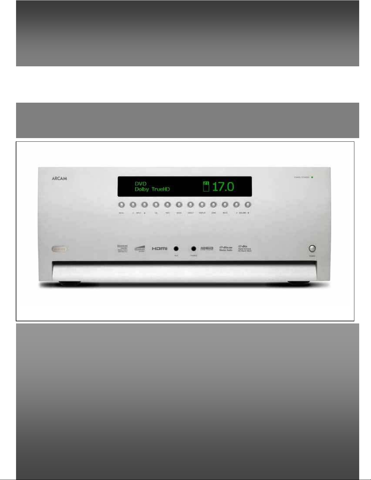
ARCAM
AVR600 Service manual issue 1.2
UA
Page 2

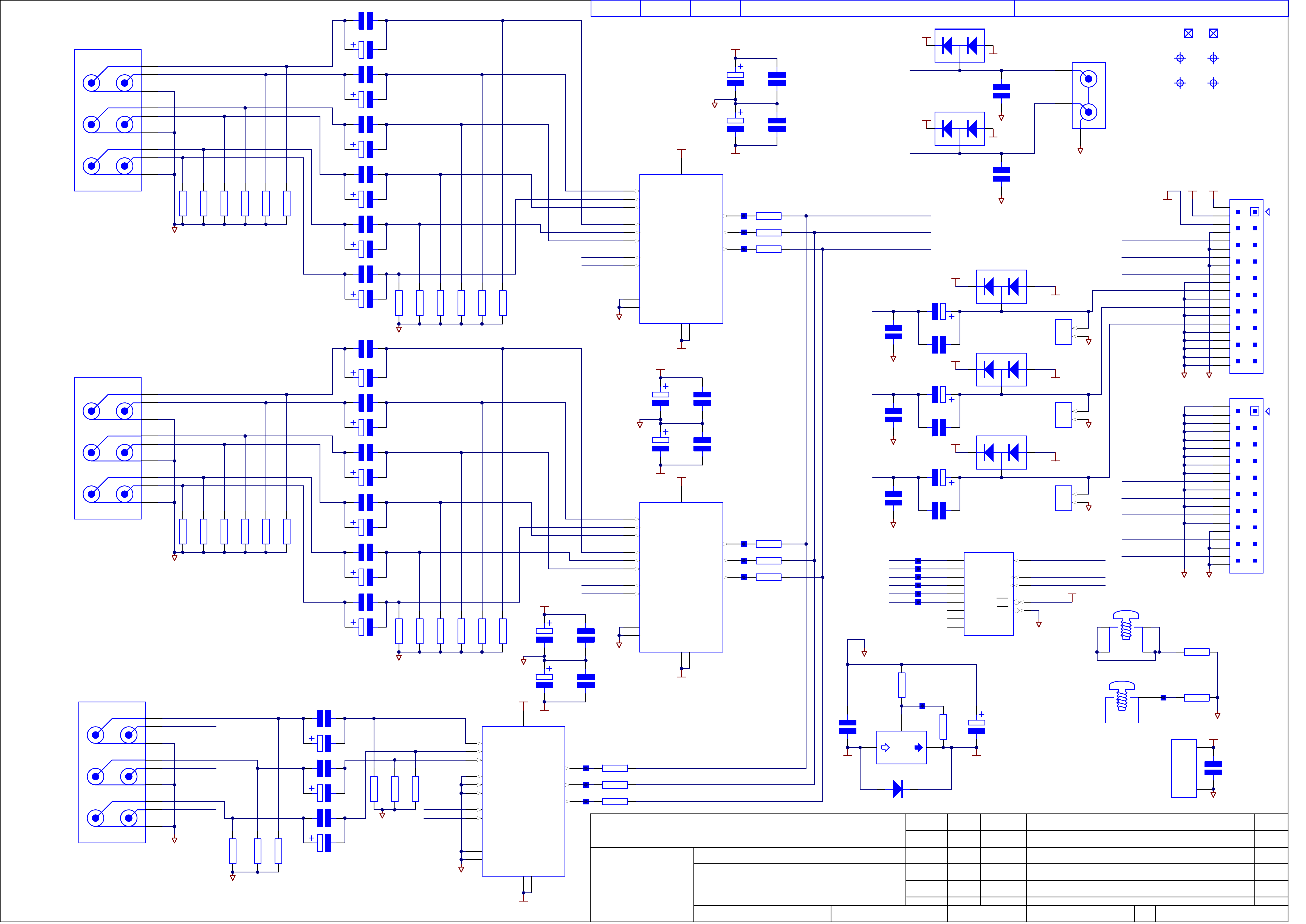
L123AY– Connection board and PSU
This PCB provides the power for the unit through CON203:
+5V_STBY – 5V standby supply L118 RS232, L126 display (on in standby)
+3V3 PW338 – L122 PW338 supply (on in standby)
1V8D – L122 PW338 supply (on in standby)
+5V_1 – general 5V supply
+6V_1 – L156 DSP, L126 Display & L119 NET supply
+40V_VFD – L126 Display
+15V – linear +15V supply
-15V – linear -15V supply
LK100 or the thermal switch from the power amp transformer is required to
pass the live mains. SW101 switches between 230V & 115V.
R101 & R102 are NTC parts to prevent inrush currents when the power amp
is turned on.
CON202 takes the Clk PSU sync signal from L121, Relay SW from L122 (to
turn on the main supplies) and /AC present back to L122. /AC present is
generated from the standby transformer secondaries with D200.D210 &
TR200. This will prevent the unit from starting if it is not low.
The standby transformer is rectified with DBR200 (GBU4K) to give
UNREG_PW338 which is used for the 1V8D (REG206 – LM2670),
3V3_PW338 (REG201 – LM2670). The 12V for the relays to switch the
secondaries are also generated from REG207 (LM7812) which is then
regulated down to give +5V_STBY REG200 (LM7805).
When the signal Relay SW is taken high by the PW338, the secondaries of
the system & power amp transformer are switched in (RLY101 & RLY102).
This enables +15V, -15V (REG204 & REG205) & +5V_1 & +6V_1 (REG202 &
REG203).
Page 3
L113AY Component Input – Output board
This PCB selects between one of five component video inputs & also provides
the output connector for Zone 3 audio.
IC100, IC101 & IC104 (LT1675CGN video buffers) require +5V & -5V. The
+5V comes direct from L123 & -5V is generated locally from the -15V supply
(from L123).
Selection of the five inputs is via IC102 (74HCT595D serial to parallel
converter, controlled via SPI Clk, Data & Vcomp latch) and IC100, IC101,
IC104. IC102 generates a /ENx signal which tri-states the output when high
and enables the output when low. When low the input is selected with the
SELx signal, high for input1, low for input2.
Truth table:
EN0 SEL0 EN1 SEL1 EN2 SEL2
0 0 1 X 1 x SAT
0 1 1 X 1 x AV
1 x 0 0 1 x VCR
1 x 0 1 1 x DVD
1 x 1 x 0 1 PVR
1 x 1 x 1 x BLANK*
*When component input is not used, BLANK should be selected.
SKT101 provides zone 3 audio output.
Page 4
L114AY – Video input – output
This PCB selects between one of five s-video & composite video inputs for the
main input & zone 2 video. It also controls the volume control for Zone 2 & 3.
The main input video is selected using IC200 (LA73031V video mux) under
the control of IC205 & IC208 (74HC595 serial to parallel converters, controlled
by SPI Clk, Data & Vid IO Mux Latch). Inputs are selected using INSEL1,
INSEL2, INSEL3 (Z2 INSEL1, Z2INSEL2, Z2INSEL3 for Zone 2 via IC203 –
LA73031V video mux).
As there is only one sync separator within each LA73031V, it is necessary to
select if this is used for S-video or composite (this means that once composite
video is selected as the source, it is not possible to autodetect S-video) SYNC CTL selects, low = Svideo, high = composite.
There are two buffered (IC201 & IC202 – BA7623F video buffers) tape
outputs, VCR & PVR which can be muted with VCR Mute & PVR Mute
respectively through a transistor network. Each output is muted when that
input is selected to prevent feedback, otherwise the output is a copy of the
composite or S-video signal going to the main zone.
Zone 2 video is buffered through IC204 (BA7623F video buffer) and can also
be mute, if required using the signal Z2Vid Mute & a transistor network.
When S-video or composite inputs are not used, V MUX STBY should be
asserted high. Note: this will disable both the main Zone & Zone 2 S-video &
composite muxes.
Video Input Truth table:
(Z2)INSEL1 (Z2)INSEL2 (Z2)INSEL3 (Z2)SYNCCTL
0 0 0 1 AV comp
0 0 1 1 SAT comp
0 1 0 1 DVD comp
0 1 1 1 PVR comp
1 0 0 1 VCR comp
0 0 0 0 AV S-vid
0 0 1 0 SAT S-vid
0 1 0 0 DVD S-vid
0 1 1 0 PVR S-vid
1 0 0 0 VCR S-vid
Volume control for Zone 2 & 3 uses IC300 & IC301 (BD3812F volume
controls) via a two-wire interface (Zone SPI Clk & Zone SPI Data). IC300 has
address D2, D1=1, IC301 has address D2, D1=0. The volume controls can
be muted from IC208 (Serial to parallel converter) using Z2 vol mute or Z3 vol
mute. The outputs are also relay controlled for powerup/down with Z2 Mute &
Z3 Mute directly from the PW338 using RLY300 & RLY301 as shunt relays.
The +7VA & -7VA required for the BD3812F volume controls is derived using
REG300 (LM1117) & REG301 (LM337LZ) from the +15V & -15V from L123.
Page 5

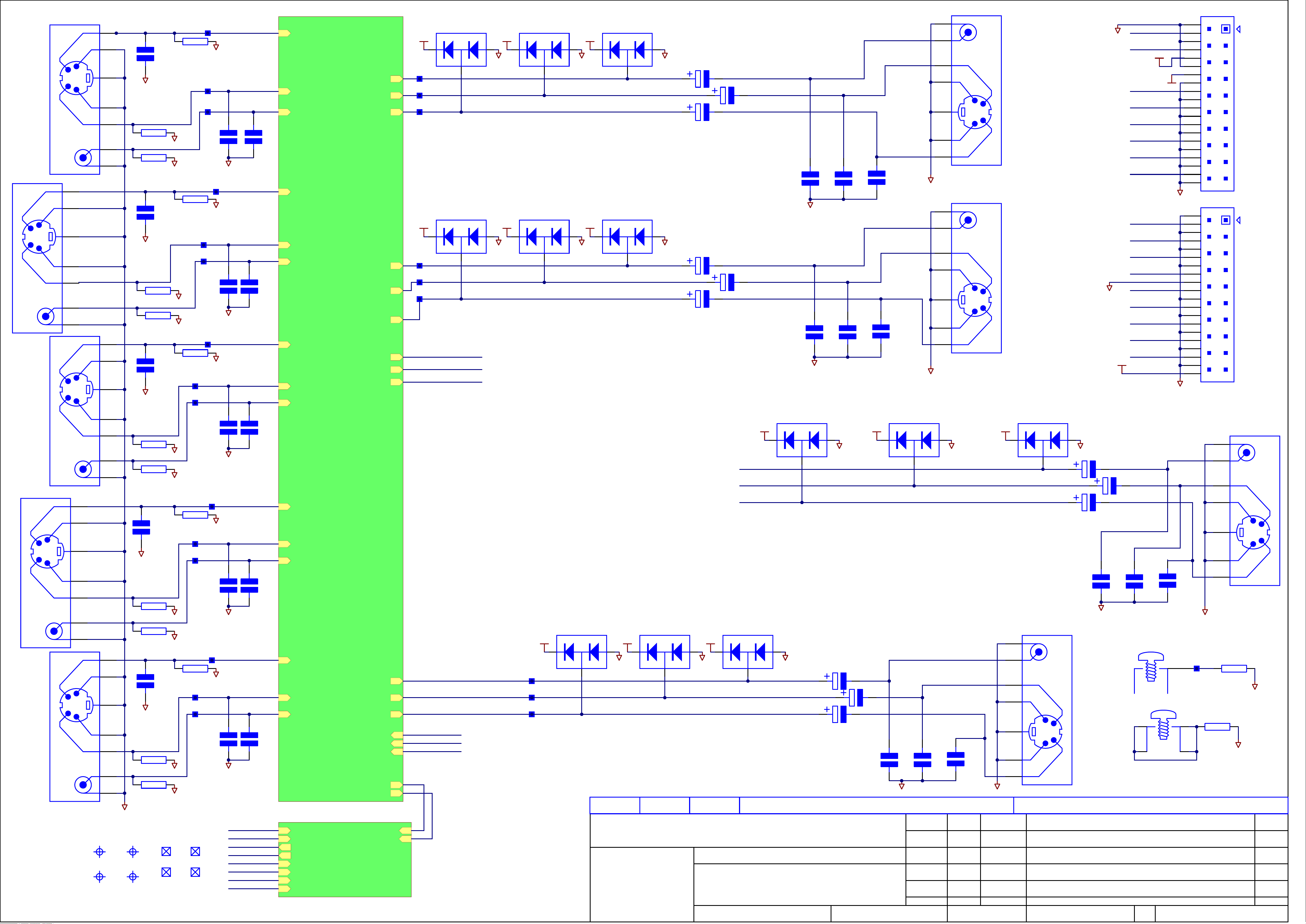
L115AY Digital Input – Output board
This PCB selects on of 8 external digital inputs or one of two internal digital
inputs & generates BClk, WClk & MClk for the DSP (see L156) & DAC (see
L117). It also generates the clocks for the ADC (see L116) when the unit is in
ADC mode.
The CD, AV & DVD inputs use coaxial connector SKT100 and feed into IC200
& IC201 (DS9637ACM buffers). The Tape, SAT, VCR & PVR inputs use
optical connectors RX100, RX101, RX102, RX103. The outputs are padded
down to give 3v3 outputs. There is also the Aux input which can be selected
(see L117), the Net input (see L119) and the HDMI SPDIF (see L122).
One of these inputs is then selected using IC202 & IC203 (74HC151 8-1 mux)
under the control of IC204 (74HC595D serial to parallel converter) controlled
by AN SPI Clk, AN SPI Data & Dig Mux Latch.
The selected input is fed to IC100 (WM8805 SPDIF Rx/Tx) which is controlled
from the PW338 via AN SCL, AN SDA & SPDIF /RESET. IC100 generates
8805MClk, 8805BClk & 8805WClk. Also, SPDIF Out which is a de-jittered
SPDIF stream which is then buffered by IC103 part A, B, C & D (parts E & F
are unused) to give both the optical output (TXC100) & 75ohmcoaxial output
(SKT101).
The selected input is also fed to IC205 part A (74HC123D monostable, part B
unused) which gives a high output from pin 13 (SPDIF_PRESENT to the
PW338) if an SPDIF signal is present.
BClk=64* WClk
MClk=128*WClk (192kHz/176.4kHz), 256*WClk (96kHz/88.2kHz), 512*WClk
(48kHz/44.1kHz) – this clock is used by the PSU to synchronise the switchers.
IC105 (XC95C36 Xilinx) generates a pre-delayed SPDIF stream from the
HDMI clocks (only MClk & WClk used) as the HDMI SPDIF is turned off
during HD audio transfer & the WM8805 does not have a zero delay PLL.
IC104 (74HCT157 Quad 2-1 mux) can also be used to re-direct the clocks
from the HDMI into the system.
IC100 (WM8805) can also operate in master mode to generate clocks for the
ADC when processing an analogue input.
3V3D is generated locally on the PCB from 5V_1 using REG200 (LM1117).
Page 6

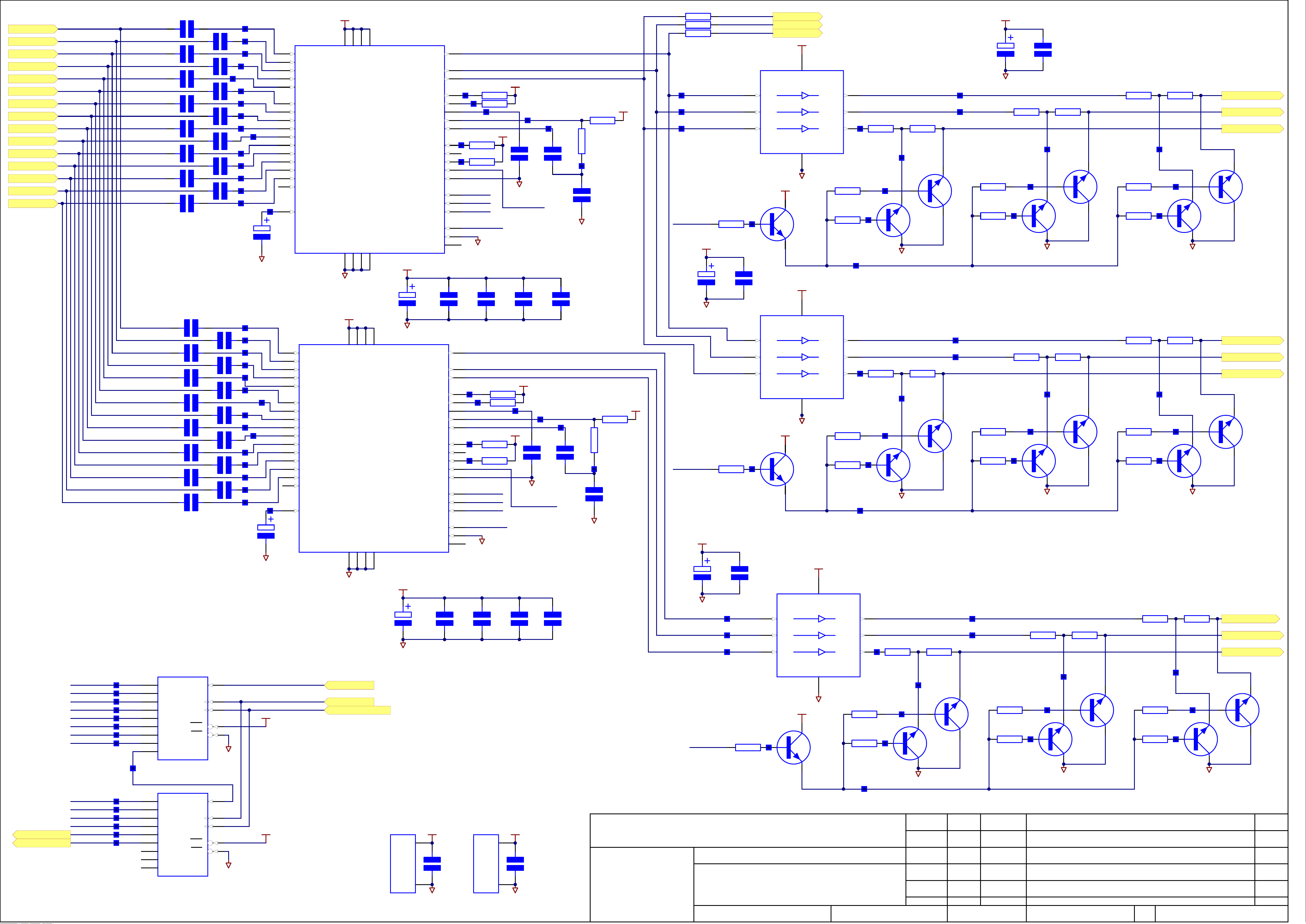
L116AY Analogue input board
This PCB selects the analogue input for the main zone & Zone 2/3 and also
digitises the analogue input for processing by the DSP / transmission over
SPDIF.
One of seven phono inputs (Tape, CD, AV, DVD, SAT, VCR, PVR), Aux
(external) input (see L127), AM/FM & DAB(internal)/Sirius(external) inputs
(see L118), Net (internal) input (see L119) and Phono (see L117).
The input for the main zone is selected using IC200, IC208, IC205, IC209
(74HC4051D 8-1 mux) under the control of IC101 & IC102 (74HC595 serial to
parallel converter), controlled by AN SPI Data, AN SPI Clk & A In Mux Latch.
The muxes operate on the virtual earth of IC203 part A (left channel) & IC206
part A (right channel), both NJM2114 op amps, inverting the signal. Part B of
these two op amps re-invert the signal (correct phase) and this output is used
by the ADC & the direct path – Main L & Main R.
IC202 (NJM2114 op amp) inverts the original output of the mux (correct
phase) to provide the three tape outputs, Tape Out, PVR Out & VCR Out.
Each of these has individual mutes – IC201, IC204, IC207 (DG413DY
analogue mux) which mutes the output if that input is selected to prevent
feedback. Otherwise, the output is the selected input. The signals for these
mutes, /Tape Mute, /PVR Mute, /VCR Mute come from IC102 (74HC595
serial – parallel converter).
Selection of the Zone 2 input is very similar, using IC300, IC303, IC302,
IC304 (74HC4051 8-1 muxes) and IC301 (NJM2114 op amp).
The Main L & Main R are connected to input AIN1A/AIN1B of IC100 (CS5345
ADC). Aux L & Aux R are also connected to AIN4A/AIN4B as this is
configurable as the MIC input and can provide power from pin25 of IC100.
the ADC is controlled from the PW338 via AN SCL & AN SDA. ADC/RESET
also comes from IC102, so the ADC can be held in reset when not being
used.
The ADC always operates in slave mode and will sample at the rate dictated
by the incoming clocks from L115 (buffered on L122). ADC Data is sent to
L115 so that it can be transmitted by the SPDIF transmitter and selected for
input to the DSP.
+12VA (REG301 LM7812) & -12VA (REG304 LM7912) for the local op amps
are derived from +15V & -15V from L123.
+5VA (used by the ADC) is derived from the +12VA with REG302 (LM1117).
+3V3D (used by the ADC) is derived from the +12VA with REG300 (LM1117).
+3V3A (REG303 LM1117) & -3V3A (REG305 LM337LZ) for the muxes are
derived from +5VA & -12VA.
Page 7

Truth table
ADC
/RST
x x x x x x x x x x 1 1 1 0 0 0 Z2 CD
x x x x x x x x x x 1 1 1 0 0 1 Z2 AV
x x x x x x x x x x 1 1 1 0 1 0 Z2 SAT
x x x x x x x x x x 1 1 1 0 1 1 Z2 DVD
x x x x x x x x x x 1 1 1 1 0 0 Z2 VCR
x x x x x x x x x x 1 1 1 1 0 1 Z2 PVR
x x x x x x x x x x 1 1 1 1 1 0 Z2 TAPE
x x x x x x x x x x 0 0 0 1 1 1 Z2 Phono
x x x x x x x x x x 0 0 1 1 1 1 Z2 Aux
x x x x x x x x x x 0 1 0 1 1 1 Z2 GND
x x x x x x x x x x 0 1 1 1 1 1 Z2 AM/FM
x x x x x x x x x x 1 0 0 1 1 1 Z2 DAB/Sirius
x x x x x x x x x x 1 0 1 1 1 1 Z2 Net
x x x x x x x x x x 1 1 0 1 1 1 Z2 Spare
x x x x x x x x x x 1 1 1 1 1 1 Z2 GND
x x x x 1 1 1 0 0 0 x x x x x x Main CD
x x x x 1 1 1 0 0 1 x x x x x x Main AV
x x x x 1 1 1 0 1 0 x x x x x x Main SAT
x x x x 1 1 1 0 1 1 x x x x x x Main DVD
x x x x 1 1 1 1 0 0 x x x x x x Main VCR
x x x x 1 1 1 1 0 1 x x x x x x Main PVR
x x x x 1 1 1 1 1 0 x x x x x x Main Tape
x x x x 0 0 0 1 1 1 x x x x x x Main Phono
x x x x 0 0 1 1 1 1 x x x x x x Main Aux
x x x x 0 1 0 1 1 1 x x x x x x Main GND
x x x x 0 1 1 1 1 1 x x x x x x Main AM/FM
x x x x 1 0 0 1 1 1 x x x x x x Main DAB/Sirius
x x x x 1 0 1 1 1 1 x x x x x x Main Net
x x x x 1 1 0 1 1 1 x x x x x x Main Spare
x x x x 1 1 1 1 1 1 x x x x x x Main GND
x 1 1 0 x x x x x x x x x x x x Tape out mute
x 1 0 1 x x x x x x x x x x x x PVR out mute
x 0 1 1 x x x x x x x x x x x x VCR out mute
x 1 1 1 x x x x x x x x x x x x No loop mute
0 x x x x x x x x x x x x x x x ADC reset
1 x x x x x x x x x x x x x x x ADC running
VCR PVR TAPE 5 4 3 2 1 0 5 4 3 2 1 0
MUTE Main Asel Z2 Asel
Page 8

L117AY Analogue output
This PCB converts the digital audio from the DSP (see L156) to analogue
audio. It also configures the use of channels 6 & 7, has the headphone amp,
has the RIAA equaliser for the Phono input and handles the multi-channel
analogue input.
The phono amplifier is a standard RIAA response and is intended for use with
MM cartridges, 5mV (check this!) output. C128 & C129 are important to
prevent the DC offset of IC100 (NJM2114 op amp) from causing problems.
IC101 forms the basis of the headphone amplifier. The output of this section
goes to L127.
IC300 (CS4385 8-channel DAC) takes multichannel data (Data LR, Data
CSw, Data SlSr, Data SblSbr) from the DSP (L156) in addition to clocks (DAC
MClk, DAC BClk, DAC WClk) from L115 (buffered on L122). Control of the
DAC is via AN SDA, AN SCL (from the PW338) and DAC /RESET (from
IC212).
The balanced outputs from the DAC are filtered by IC400, IC401, IC402,
IC403 (NJM2114 op amps). All channels are identical except for the
subwoofer, which has 10dB (check this!) gain.
Left & right inputs to IC204 (CS3318 volume control) are multiplexed between
the filtered DAC output, the Main L & Main R direct analogue inputs (from
L116) and the left & right multichannel inputs (SKT200) with IC200
(74HC4052 dual 4-1 mux). This mux operates on the virtual earth of IC201
(NJM2114 op amp) and also provides the signals Mux L & Mux R.
The centre input to IC204 (CS3318 volume control) is multiplexed between
the filtered DAC output and the centre multichannel inputs (SKT200) with
IC203 (74HC4053 triple 2-1 mux). This mux operates on the virtual earth of
IC205 part A (NJM2114 op amp).
Subwoofer, surround left & surround right inputs to IC204 (CS3318 volume
control) are multiplexed between the filtered DAC output and the subwoofer,
surround left & surround right multichannel inputs (SKT200) with IC214
(74HC4053 triple 2-1 mux). This mux operates on the virtual earth of IC201
(NJM2114 op amp) part A (subwoofer) & IC207 (NJM2114 op amp - Surround
left & surround right).
IC213 selects between the filtered DAC output of surround back left / right,
surround back right / left multichannel inputs, Z2 L / Z2R and Mux L / Mux R.
This allows the use of channels 6 & 7 as either surround back left/right in the
main zone, or powered Zone 2 outputs, or bi-amped left/right in the main
zone. This mux operates on the virtual earth of IC209 (NJM2114 op amp).
IC204 (CS3318 volume control) is controlled by AN SCL, AN SDA (from the
PW338) and VOL /RESET & VOL /MUTE from IC212.
Page 9

Truth table
Sel0 Sel1 Sel2 Sel3 Sel4 Vol /RST Vol /Mute DAC /RST
0 0 0 0 0 1 1 1 DAC output
1 0 x x x 1 1 1 L/R analogue direct
0 1 1 1 0 1 1 1 MCH output
x x x 0 1 1 1 1 Sb=Zone 2
x x x 1 1 1 1 1 Sb=L/R
x x x x x 0 x x Volume control reset
x x x x x 1 0 x Volume control mute
x x x x x x x 0 DAC reset
The output of the volume control is buffered through IC202, IC206, IC208,
IC210 to remove any DC offset before going to CON100 (connection to the
power amp) and SKT100 & SKT100 phono outputs sockets. Shunt relay
muting is provided for power on/off, controlled from the PW338 (Main mute &
Sblr/Sbr mute).
Page 10

L118AY – IR – Trig – DAB/FM - RS232
This PCB handles the following functions:
RS232 communication with the PW338
iPod RS232 control (compatible with rLead & rDock)
Sirius satellite radio (US)
Z1, Z2, Z3 12V triggers
DAB
AM/FM
Z1, Z2, Z3 IR inputs.
CON102 & IC102 (MAX3232 RS232 converter, part1) provide the RS232
communication with the PW338 – used for RS232 control or updating. Note,
the signals RS232 Tx & RS232 Rx are labelled relative to the PW338, so
RS232 Tx is the Tx FROM the PW338.
CON105 & IC102 (MAX3232 RS232 converter, part2) provide the iPod RS232
communication. Pin 9 of CON105 (/iPod Present to PW338) is taken low
when an rLead is connected. Note, the signals iPod Tx & iPod Rx are
labelled relative to the UART (IC403, L122), so iPod Tx is the Tx FROM the
UART.
SKT101 provides the Sirius RS232 communication. Note, the signals Sirius
Tx 232 & Sirius Rx 232 are labelled relative to the UART (IC403, L122), so
Sirius Tx 232 is the Tx FROM the UART.
SKT101 also provides the +5V for the Sirius Home Connect module, so the
module does not require external power. This power comes from the +5V_1
(L123) and is connected to pins 1 & 2 of SKT101 as power & host presence.
Analogue audio also passes through this socket, so this is the only connection
to the Sirius module.
There are three triggers, Zone1 , Zone 2, Zone 3. These give a 12V 100mA
output when activated from IC101 (74HC595 serial to parallel converter). The
signals Z1 Trig, Z2 Trig & Z3 Trig are active high.
DAB uses the Gyrosignal 1122 module. As this module is normally controlled
via RS232, a CPLD, IC100 (XC95C36 Xilinx) is used to provide I2C control
from the PW338 (DAB SCL & DAB SDA). Due to an issue with the
Gyrosignal implementation of I2C within their CPLD, IC103 (SN74HC1GU04
single inverter) is required to invert the DAB SCL signal. The DAB module
gives an analogue output which is buffered through a ground balancing circuit
(IC301 NJM2114 op amp) – this section is also used for the Sirius analogue
output. DAB /RESET comes from IC101 (74HC595).
AM/FM uses the ALPS module. Different modules are fitted depending on
region – Europe (with RDS), US (no RDS), Japan (different FM range).
Control is direct from the PW338, FM CE, SPI Data, SPI Clk. Also, /RDS On
from IC101 (74HC595) is used to turn off the RDS chip in EU modules when
the AM band is used (the RDS chip running on AM interferes with AM
performance). RDS Int & Data come from the Alps module to the PW338 for
Page 11

EU FM transmissions carrying RDS data. VSM goes to an ADC on the
PW338 and provides a signal strength indication. The AM/FM module gives
an analogue output which is buffered through a ground balancing circuit
(IC302 NJM2114 op amp).
IR from the front panel comes onto this board from L126 and goes through a
re-modulator circuit (IC200 LMC555) as it has been demodulated on the front
panel. This signal, Z1 remod, goes through SKT200 such that inserting a plug
into SKT200 will stop this signal (to prevent conflicting signals if a Zone 1
external IR sensor is used) from going to LED200 and then being
demodulated by RX200.
Zone 2 (SKT102) & Zone 3 (SKT103) IR inputs drive LED201 & LED202
which are demodulated by RX201 & RX202.
Zone 1, Zone 2 & Zone 3 are also multiplexed together to give IR Out through
TR207 & SKT104.
The ground balancing circuit uses +5V_1 from L123 and generates -5V from
IC303 (SP6661EN charge pump). The AM/FM module uses +9V_FM,
generated with REG202 (LM317) from +15V (from L123). +12V_IR is
generated from +15V (L123) using REG200 (LM7812) and runs the IR output
& 12V triggers. +5V_STBY (L123) generates +3V3_STBY with REG201
(LM1117) – used by IC102 (MAX3232) so the RS232 comms are still
available in standby. +3V3_D is generated from +5V_1 (L123) with REG203
and is used by the DAB module.
Page 12

L119AY NETWORK
This PCB handles the network connectivity & USB support. Telnet control
(Ethernet to RS232 tunnelling) is also handled by this PCB.
IC102 (DM850 audio processor) does not have any internal boot code, upon
being powered, it starts the BFL (First level bootloader) from the FLASH
memory IC202 (S29GL064A90TFIR30). This then executes the BSL (second
level bootloader) which brings up the network support. The second level
bootloader then executes the application. The BFL should never need to be
updated and as such will not be included in the standard upgrading
application.
The FLASH memory is also used to store settings, such as the Arcam specific
Cardea keys & MAC address. Note: if the FLASH device is ever changed, it
is essential that the original MAC address be programmed into the unit so that
the user does not lose and internet radio stations/favourites groups.
The device also uses SDRAM (not until the BSL executes) – IC200
(IC42S16800-6T(G)).
Wifi connectivity is via an Edom module and plugs into CON300. Note: this
module is specific to this unit and cannot be substituted, spares must come
from Arcam.
Wired Ethernet uses IC400 (DM9161A MAC), L401 (TS6121C magnetics).
The Ethernet connector (CON400) does not have any link or act LEDs as
these were thought to be potentially annoying in an AV environment.
In addition to the SPDIF audio output, there analogue audio is generated from
NET MClk, NET BClk, NET WClk & NET Data0 using IC501 (CS4345 DAC).
IC500 (LM358AM op amp) buffers & filters the output of the DAC. The output
can then be muted under control of the DM850 (/MUTE) and then ground
balanced with IC502 (NJM2114 op amp).
The DM850 uses two switching regulators for generating the +3V3D
(REG600) and 1V8 (REG601). IC601 (SP6661 charge pump) generates the 5V used by the ground balancing circuit – IC601 has a 4V7 zener regulator
circuit supplying it.
Page 13

L121AY – Connection board
This PCB provides the connections between all the daughter cards, plus the
main PCB (L122).
IC300 & IC301 (74HC244 buffers) take the clock signals (WClk, BClk & MClk)
from L115 & DSP WClk Out & DSPBClk Out from L156 and buffer them to the
ADC, DSP & DAC.
IC303 (74HC4040 divider) divides the MClk down to provide Clk PSU to sync
the switchers on L123.
Page 14

L122AY Main Board
This is the main PCB with the PW338 handling the control of the entire unit,
as well as video processing. HDMI Rx & Tx functions are performed on this
PCB as well as video encoding & decoding.
IC200 is main PW338 micro/video processor. On sheet 4 the microprocessor
interface is shown. The PW338 has no internal boot code, so relies on code
in IC401 (39VF3201 FLASH) to run. IC401 is required to be pre-programmed
with at least boot code. If this part requires replacement, it *must* be
programmed with at least the boot code. If the FLASH is programmed with
the boot code, upon starting up, the PW338 will send out a boot loader
message on the RS232 port0 (sheet 3) at 115.2k baud, 8bits, no parity. If
there is a problem with the DDR memory (IC600 & IC601 sheet 6) there will
be a message sent along with the boot loader message. /AC present (low)
and Poweron_reset (high) from IC402 (LM809M-2.93 – resets the micro if
3V3_PW338 drops below 2.93V) are also required for the PW338 to start.
IC400 (74HC4040 divider) pre-divides the wordclock so the PW338 (EXINT0)
can measure the sampling frequency of incoming digital audio sources. RDS
Int (from L119) is connected to EXINT1 as the RDS data is streamed out of
the ALPS AM/FM module regardless of the readiness of the PW338.
IC403 is a quad UART to provide RS232 communication with the network
(L119), the Sirius satellite radio (L118) & iPod (L118). All signal labels are
with respect to the PW338.
Sheet 7 shows most of the connections to the daughter PCBs as well as the
I2C control busses:
EDID – used for the EDID dual port EEPROM (IC909, sheet 9)
AN – Analogue control bus, L116 Analogue input & L117 Analogue output
HDMI_Config – SiI9135 & SiI9134 x 2 & ADV7310 (sheet 5)
DAB – DAB module (L118) & system EEPROM (IC706 sheet 7)
3 x 74HC595 (IC701, IC703 & IC704) provide additional control output
signals.
The remaining control signals are on sheet 2. This sheet also shows the
interface between the SiI9135 HDMI receiver (IC201) and the PW338. The
audio outpus of IC201 go through L121 (Connection PCB) to L115 (Digital
IO).
Sheet 3 shows the analogue video inputs. There are separate inputs for
composite, S-video & component. The Y signal also is taken to a Sync input
on the PW338.
Sheet 5 is the video output port. The digital video port of the PW338 is
connected to the ADV7310 (IC501), SiI9134 (IC502) & SiI9134 (IC503). The
ADV7310 converts the digital video to analogue video outputs for component,
S-video & composite (depending on the resolution – up to 1080i for
component, 480i/576i only for composite & s-video). The two SiI9134 parts
convert the video data to HDMI serial data. While it is possible to have all
Page 15
video outputs active, resolution & copy protection limits apply. Also, when
displaying 408i/576i the colour space requirements of the ADV7310 &
SiI9134s are incompatible, so if an HDMI display is connected the analogue
outputs are muted.
The PW338 can only output one clock pulse per pixel, so for 480i & 576i
resolutions, a video clock doubler is required (IC504 ICS2402MLF) to convert
the 13.5MHz pixel clock (Display Clk) to 27MHz (Display Clk2) under the
control of Vid_Clk_Sw.
The output of the ADV73120 is filtered by IC500 (ADA4410). Also, the Svideo signals are recombined to form the composite output signal (Cvid out).
The outputs of this part are series terminated with 75ohms before going to
L133 (component IO) & L114 (video IO) via L121 (connection PCB).
Sheet 9 shows the 5 HDMI inputs.
The serial data differential pairs are multiplexed with IC901 & IC903
(PI3HDMI413). The DDC lines are multiplexed with IC907 & IC910
(DG408LDY) for connection with the dual port EEPROM (IC909) and the
HDMI receiver (IC201).
The CEC line is multiplexed with IC911 (DG408DLY)
The +5V line is multiplexed with IC912 (DG408DLY)
Hotplug out is controlled by IC900, IC904 & IC906 (74HCT08 AND gate)
which give individual hotplug control & also global control with PW338
hotplug.
All these multiplexes must operate together for an HDMI input to be correctly
selected.
TMDS Mux
Sel3 Sel2 Sel1 Sel0
0 0 0 0 SAT
0 0 0 1 AV
0 0 1 0 DVD
0 1 1 1 PVR
1 0 1 1 VCR
1 1 1 1 Blank
DDC/CEC/+5V Mux
Sel2 Sel1 Sel0
0 0 0 Blank
0 0 1 AV
0 1 0 SAT
1 1 1 DVD
0 1 1 VCR
1 1 1 PVR
Hotplug Mux
SelPVR SelVCR SelDVD SelSAT SelAV
0 0 0 0 0 Blank
0 0 0 0 1 AV
0 0 0 1 0 SAT
Page 16

0 0 1 0 0 DVD
0 1 0 0 0 VCR
1 0 0 0 0 PVR
Sheet 10 shows the ESD protection devices (IC1000 & IC1004 CM2020) for
the two HDMI outputs. There is also provision for turning off the 5V signal to
the display device through FETs M1000 & M1001.
The two 120 way connectors on sheet 11 show all the connections between
the L122 PCB and L122.
Page 17

L124AY – Speaker board
This conducts the output signals from the power amplifiers on both L125 and
L129 to the speaker terminal blocks LS100 – LS103 inclusive, via 4 double
pole relays RLY100 – RLY103. The 24V dc supply from the relays is fed from
L129 via CON101 pin 18, returning to ground via pin 17. The relay switching
transistors are TR100 – TR 103 and the logic level signals to control these
also enter via CON101 pins 19 and 20. Note that the SBL and SBR channels
are switched independently from the other 5 channels, as these can be reassigned in software to support zone 2 in stereo if required.
Zobel networks, comprising 1 uH air cored chokes in parallel with 4R7 2 Watt
resistors, are in series with all outputs to isolate the power amplifiers from
capacitive cable loads which might otherwise provoke instability.
L125AY – Power amp upper
This contains all the power amplifier electronics for the Centre (C), Left
Surround (LS) and Right Surround (RS) channels. It also contains the power
supplies for all 7 channels, which are fed directly from the secondaries of the
power transformer L951TX as raw AC, via CON106, to the bridge rectifiers
DBR201 and DBR202 and two reservoir capacitor banks, C206/7 plus
C210/213 for Vcc/Vee, and C214/5 plus C220/1 for +Vlo and –Vlo.
The power amplifier design is Class G, which is why two sets of power rails
are employed; Vcc and Vee are approximately +/- 59V off load and +Vlo and
– Vlo are approximately +/- 30V off load.
The rectified and smoothed power rails are fed to the lower power amp PCB
L129, along with an AC power feed for checking the mains is present, via
CON100.
CON103 is used to bring in the C, LS and RS line level input signals from the
rest of the AVR via L129. It also imports +/-12V supplies for the front stage
op-amps and +5V for the top heatsink temperature sensor IC400. Outputs
comprise this sensor’s signal and two DC offset protection lines (ERR_POS
and ERR_NEG), which are returned to the system microprocessor via L129.
CON105 carries the C, LS and RS outputs to the Speaker PCB L124. It also
carries the speaker ground returns for all 7 channels back to the star ground
point on L125.
All 7 power amplifiers are identical, except for the Centre channel where only
one half of its set of the various dual driver ICs is used.
Each power amplifier is topologically split into two halves – the input stage IC,
LM4702 high voltage driver IC and DC servo IC comprise the driver stage
(e.g. U_driver_C); the power transistors plus their drivers and protection
circuitry comprise the output stage (e.g. U_PA_C), as shown in the L125
block diagram.
Page 18

Additionally the 3 power amplifier channels in L125 share a common pair of
power MOSFET lifters (the part of the block diagram shown as U_Lifter_C)
which control the amount of output voltage fed to the collectors of the power
transistors in the 3 power amplifiers.
The Centre channel Driver Stage
converter IC700B (one half of an NJM2114) which rejects common mode
noise on the input when grounded to AGND_FF via the handbag link
CON700. Its output feeds one half of the stereo high voltage driver IC
(LM4702C - IC701) via the low pass network R706 and C704. The LM4702 is
used in a non-inverting configuration and provides all the voltage gain of the
system, set by R713 and R704. Pins 11 and 12 of IC701 feed the inputs of the
negative and positive halves of the Output Stage. The dominant pole
compensation is set by C705, C713/R714 provides some second order
feedback in the audio band to provide a higher open loop gain at high audio
frequencies and thus reduce hf distortion. R715 and R716 (without TR700
which is a “no fit”) provide some extra voltage to IC701’s negative supply at
high negative output voltages via a bootstrap arrangement in the output stage
to prevent premature clipping of the negative half of the output. Note that the
heatsink of IC701 is connected to its negative rail – this must NOT be
accidentally shorted to ground!
Good power supplying decoupling of IC701 is essential and is provided by
C701, C708, C709, C712 and C714.
Note that the amplifier is DC coupled throughout. IC702B (one half of a
TL072) has a very high input impedance and forms a ground referenced
inverting integrator with R712 and C711; their time constant is approximately
1.5 seconds. Its output is fed back to the positive input IC701 via the
attenuator R711 and R706 to keep the DC output of the amplifier close to
zero. It can also correct moderate DC offsets appearing at the input of
IC700B. Should these become excessive, or should a circuit fault cause
significant DC at the loudspeaker output, then the error voltage at the output
of IC702B will feed through to the system microprocessor via D700 (which
works in conjunction with the similar diodes in the other power amplifier
channels as a wired OR gate) to generate a system shut down signal.
starts with the balanced to unbalanced
NB. R702 will also mute the power amplifier electronically in the absence of
the +/- 12V supply.
The Centre channel Output Stage
classic emitter follower configuration, with enhancements to ensure near class
A operation at power levels of up to about 10 watts. Both the positive and
negative halves are essentially identical.
The pre-driver and driver transistors are connected to the high voltage rails
Vcc and Vee (approx +/-59V). However because this is a Class G design the
output transistors TR406A and TR409A normally run at half these voltages
(+Vlift and –Vlift, approx +/- 30V) connecting to the +Vlo and –Vlo supplies via
Shottky power diodes D100 and D101 shown on the main block diagram.
When the amplifier is required to deliver more than about +/- 25V peak
comprises complementary triples in a
Page 19

(equivalent to about 30Watts rms into 8 ohms) then the lifters (fed from Vcc
and Vee) are progressively powered on to maintain a constant 5V or so
across the collector-emitter junctions of the output transistors.
Note that on L125 the lifter outputs are shared between all three power
amplifiers for reasons of economy and space – whereas the lifters on the
other 4 channels on L129 are only shared between two power amplifiers
each. Since the worst thermal stress on the lifters occurs at output powers
somewhat above 30W rms equivalent into 8 ohms, we do not recommend
testing the amplifier for extended times with continuous signals in the 30 - 50
Watts range with all three channels (C, SL and SR) running simultaneously
and driving into low impedances. This is especially true of square wave
signals! The thermal sensor IC400 is located close to the lifter MOSFETs in
order to monitor this condition.
The power transistors TR406A and TR409A have built in thermal
compensation diodes (TR406B and TR409B) which form part of the biasing
network. The thermal sense biasing transistors TR401 and TR416 are thus
mounted adjacent to (and ideally in intimate contact with) the driver transistors
TR403 and TR414 so that as they warm up the bias remains relatively stable.
(In practice it rises somewhat, but predictably so, as the drivers warm up).
The pre-drivers, TR400 and TR415, are in a DC feedback loop with TR401
and TR416, so no thermal drift in bias occurs from these. Bias is set by
RV400; D403 and R421 ensure that no catastrophic increase in bias will take
place if RV400 fails open circuit.
Optimum bias at quiescent operating temperature is measured across the two
0.1 ohm emitter resistors forming R408 – it is typically 15mV at the pins of
C400. When setting up from cold a good starting point to achieve this is to first
turn RV400 to minimum (i.e. fully anticlockwise) and then slowly turn it up to
6mV.
The transistors TR405A and B and their associated networks provide
comprehensive two slope safe operating area (SOA) protection for the output
devices. When the prescribed combination of voltage and current across
TR406A or TR409A is exceeded, the relevant protection transistor conducts
and shorts out the base drive to the associated pre-driver, thus limiting the
dissipation in the output device. The output of each channel of the LM4702 is
current limited to about 5-10mA so no damage can occur to it under these
conditions. Note that if an output device fails short circuit then the 7 Amp fuse
in its collector will fail – the driver transistors TR403 and TR414 will then try to
take over and so are protected by 1 ohm fusible resistors in their collectors.
Note that the heatsinks of the drivers TR403 and TR414 are “live” – an
accidental short to ground here with a test probe will probably blow the
associated 1 ohm fusible resistor.
Diodes D402 and D405 protect the output transistors from being reverse
biased in the presence of inductive load “spikes”. Diodes D401A/B form part
of a wired OR gate system with the other power amplifier channels on L124
and are used to drive the lifters connected to the collectors of TR406A and
TR409A. R439 and C411 are part of a bootstrap network for the negative rail
of IC701 and its associated pre-driver transistor TR415. R417 and C406 are
Page 20

a Zobel network (sometimes called a Boucherot cell) to help compensate for
inductive loads at high frequencies.
The Class G Lifters
TR602 plus p-channel power MOSFET M601 for the positive half, and TR603,
TR604 and TR605 plus n-channel power MOSFET M603 for the negative half.
They are arranged as CFPs (complementary feedback pairs) rather than plain
emitter (source) followers so that the MOSFETs can be fully turned on without
needing power supplies that exceed Vcc and Vee.
The two halves operate identically – we will examine the positive (top half)
lifter to see how it works. With only small signals coming from the power
amplifier, node PLD_C remains biased at about +20V (via the network R614,
D600, R602., R603, R605) whilst node +VLIFT_C is held at approximately
+30V (i.e. +Vlo less the 0.2V or so dropped across the Shottky power diode
D100). The emitter of TR602 meanwhile is at about +24.5V, so TR602 is
turned hard off. Thus the base of TR600 is connected via R600 to Vcc and the
emitter is at Vcc – 0.6V. Vgs of M601 is thus -0.6V which is well under the
approx -2.5V required to turn on M601.
When the voltage at node PLD_C exceeds approximately +25V this is enough
to turn on TR602. When about 3V is developed across R600 this is enough to
turn on M601 which conducts until the voltage at the emitter of TR602 has
risen enough to stabilise the system. The output voltage then can rapidly track
the input (plus about 5V) as required, reverse biasing the Shottky power diode
D100 and drawing the collector current for TR406A via M600 and the +Vcc
supply. The complementary emitter follower TR600, TR601 ensured the gate
capacitance of the MOSFET can be both charged and discharged very
quickly. C605 provides fast local decoupling to minimise switching transients.
are in two complimentary halves – TR600, TR601 and
Page 21

L129AY – Power Amp lower
This contains the power amplifier electronics for the Left (L), Right (R),
Surround Back Left (SBL) and Surround Back Right (SBR) channels. It also
contains housekeeping logic for the amplifier protection system and power
drive circuits for the protection relays and cooling fans.
The power amplifiers are essentially identical to those in L125, except that the
lifter circuits are only shared between pairs of power amplifiers (L and SBL, R
and SBR respectively) rather than all three channels in L125. They receive
their raw DC power voltages from L125 via CON100. Please refer to the
description of the Centre Channel (C) power amplifier (in L125) for a detailed
understanding of the circuitry of the power amplifiers in L129.
CON102 carries the L, R, SBL and SBR output signals to the speaker board
L124. It also delivers +24V DC power and logic level switching signals to the 4
speaker relays on L124. NB - the ground returns shown on CON102 do not
carry L129’s main speaker currents back to the star point (which is located on
L125) but are merely used for the L, R, SBL and SBR amplifiers’ optional
extra Boucherot networks located on L124.
Note that it is L129 which communicates with the rest of the receiver, via two
ribbon cables connected to CON101 and CON 103. CON 101 receives 7 line
level input signals, and low voltage supplies (+12V, -12V and +5V) from L117.
CON101 also inputs the speaker relay mute signals for L124. CON103
supports temperature and DC offset monitoring for L125 and L129, plus a fan
drive signal, sent to and from the system microprocessor on L122, via L121.
The heatsink temperature monitors on L129 are IC800 and IC900; these are
located between the relevant pairs of lifter power MOSFETs.
TR102 provides nominal +24V power to the output relays on L124, via the
unregulated +30V supply on L125. The 27V zener diode DZ102 prevents
excessive voltage being applied to the relays in the event of high mains
voltages.
REG 101 is not normally used as links CON109 and CON110 are omitted in
production. It provides +5V for the on board logic and temperature sensors if
no +5V line is present (e.g. during development testing).
TR1003A/B and TR1001 together make a fan driver with a DC gain of 10, so it
can be triggered with a 3V3 microprocessor signal. Power comes from the
unregulated +Vlo supply (approx +30V). The fans are two 12V DC units
connected in series fed from CON107 and CON108.
IC1000 is a triple 3-input NAND gate. To switch on (i.e. unmute) the speaker
relays, all 3 inputs on IC1000B (for LSB and RSB channels) and/or IC1000C
(for the other 5 channels) must be high. The 3 inputs come from:
(a) the AC present detector based around TR1002 and IC1000A,
(b) the ERR_NEG and ERR_POS detector, based around TR1004A/B, which
detects excessive DC offsets on any one or more of the 7 power amplifier
channels and (c) the ~MUTE_SB and ~MUTE_REST lines under the control
of the system microprocessor.
Page 22

L126AY – Front Panel
This PCB handles the VFD, keyboard scan, IR reception for the front panel &
power LEDs.
The micro is an Atmel AT91SAM7S32 (IC101) which must be initially
programmed via the Atmel/Segger debugger via CON101. Subsequently, the
micro can be reprogrammed from the PW338 using the Arcam upgrader utility
over RS232. The bootloader should never need to be updated and as such
will not be included in the standard upgrading application.
Communication with the PW338 is via RS232 – IC101 sends information on
keypresses to the PW338 & receives information to display & brightness
commands from the PW338 – FP_TX & FP_RX. Note these signals are
labelled with respect to the PW338.
IC101 uses +3V3_PW338 so is powered in standby. It has an internal 1V8
regulator which generates VDD_OUT (1V8, pin 8) which is decoupled &
powers the core & PLL of IC101 (pins 18, 41 & 48).
The VFD (DISP100) is driven from serial data SIN from IC101
(AT91SAM7S32 micro). The serial data is gated through IC102 (74HC08
quad NAND gate, parts C & D unused) controlled by SIN1_CTL & SIN2_CTL
from IC101 to provide dimming of the display. The output data from IC102 is
clocked into the display with the signal CLK from IC101 and is latched into the
display during the blanking period (LAT & BLK).
The VFD filament drive is synchronous with the display update. Signals
FClock1 & FClock2 are 180deg out of phase and drive IC100 (AD8532 op
amp) to give a 6V oscillating drive to the two ends of the filament (from +6V_1
– L123). The HT is provided direct from L123 (+40V_VFD). +6V_1 &
+40V_VFD are not present in standby.
IR decoding (RX100) is powered by +5V_STBY, allowing IR reception when in
standby. The signal pass through L121 (Connection) to L118 (Trigger) before
going to L122 (Main PCB).
The power LEDs are fitted to a small snap-off PCB that is connected via a 3
wire lead. Green LED when the unit is on, Red when in standby, both during
power on.
Page 23

L127AY Front Input
This PCB handles the auxiliary input & headphone output.
SKT101 carries the headphone output from L117 (Analogue output). There is
also a switch to sense the headphones being inserted. The pullup resistor for
this is on L122, so if L127 PCB is not fitted or the cable not fitted, the unit will
sense the headphones are permanently inserted.
SKT100 is the microphone, auxillary input (to L116 Analogue input) & also
has an optical input for digital sources (Aux SPDIF to L115 Digital input) using
a 3.5mm optical lead.
L156AY – DSP board
This PCB handles the audio decoding of digital inputs & processing of
digitised analogue sources.
IC100 (ADSP-21366 DSP) handles the main decoding, including the new HD
formats. Data is either from I2S Data (SPDIF/ADC data from L115) or MCH
Data0, MCH Data1, MCH Data2, MCH Data3 from L122 (Main PCB). In both
cases, the clocks DSP WClk, DSPBClk & DSP MClk are required.
The code for IC100 is held in IC103 (S29AL016D FLASH). The DSP also
requires SRAM (IC101, IC104 71V424S SRAM). The address/data bus is
multiplexed through IC102 & IC106 (74LVC573 buffers) controlled by ALE.
Additional memory decoding is handled by IC105 (74LVC139 2-4 decoder).
R121 & R103 (0R0) should be fitted to allow the DSP to boot in SPI mode.
R117 (4k7) sets the internal clock multiplier to 16:1 (16*20MHz = 320MHz).
IC201 (ADSP-21367 DSP) handles the post-processing & room EQ. Data is
sent in multichannel format regardless of the input between IC100 & IC201
(DSP2 LR, DSP2 LsRs, DSP2 CSw, DSP2 SblSbr). The data is clocked in
using DSP2 BClk & DSP2 WClk, generated by IC100 & DSP MClk from L121.
Data is then clocked out to the DACs (Data LR, Data SlSr, Data CSw, Data
SblSbr) with clocks DSP BClk Out, DSPWClk Out which are buffered on L121
before going to L117 (Analogue Out).
Communication with the PW338 is via a single SPI bus:
DSP Clk - clock
DSP MISO – data from PW338
DSP MOSI – data to the PW338
DSP1 /CS – select DSP1
DSP2 /CS – select DSP2
DSP1 FLAG0 – signal back to PW338
DSP2 FLAG0 – signal back to the PW338
Note: DSP reset is by asserting both /CS lins low simultaneously (IC107
74LV1G32 single Or gate).
Page 24

Power for the DSPs comes from two regulators 3V3 (REG300), further
regulated to 1V2 (REG301). Both are heatsinked.
Page 25
SAT IN
VCR IN
AV INDVD IN
PVR IN
Pr
Pb
Y
Pr
Pb
Y
Pr
Pb
OUT
Y
SKT100
D
EF
JYE TAI
GOLD
SKT102
D
EF
JYE TAI
GOLD
SKT103
JYE TAI
GOLD
50V
X7R
50V
D3c
ABC
RG B
A2b
X7R
A/D1a
E3c
B2b
50V
X7R
B/E1a
F3c
C2b
50V
C/F1a
VGND
R100
R101
R102
75R
75R
75R
75R
75R
75R
0W063
0W063
0W063
0W063
0W063
0W063
R103
R104
R105
50V
X7R C112
D3c
ABC
RG B
A2b
X7R
50V
X7R
10N
50V
X7R
50V
X7R
A/D1a
E3c
B2b
50V
X7R
B/E1a
F3c
C2b
50V
X7R C128
50V
X7R C131
50V
X7R C133
D
C/F1a
0W063
R121
VGND
D3c
ABC
RG B
A2b
R122
Pr Out
R123
75R
75R
75R
75R
75R
75R
0W063
0W063
0W063
0W063
0W063
0W063
R124
R125
R126
50V
X7R C135
10N
A/D1a
E3c
EF
B2b
Pb Out
50V
X7R C139
10N
B/E1a
C136
2U2
C142
2U2
10N
10N
10N
50V
YK
50V
YK
F3c
C2b
Y Out
50V
X7R C143
10N
C/F1a
R141
R142
R143
C144
2U2
50V
YK
VGND
75R
75R
VGND
75R
0W063
0W063
0W063
C100
10N
C101
2U2
C102
10N
C104
2U2
C105
10N
C106
2U2
C107
10N
C109
2U2
C110
10N
C111
2U2
C113
2U2
50V
YK
C117
10N
C118
2U2
C120
10N
C122
2U2
C124
10N
C126
2U2
C130
2U2
C132
2U2
C134
2U2
50V
YK
R109
VGND
50V
YK
50V
YK
50V
YK
50V
YK
50V
YK
R112
VGND
50V
YK
50V
YK
50V
YK
50V
YK
50V
YK
R130
VGND
R110
47K
47K
47K
0W063
0W063
0W063
R113
R131
R111
/EN2
SEL2
R114
47K
47K
47K
47K
47K
47K
0W063
0W063
0W063
0W063
0W063
0W063
R132
47K
47K
47K
47K
47K
47K
0W063
0W063
0W063
0W063
0W063
0W063
VGND
R115
R133
1
2
3
6
7
8
9
10
4
5
R116
R134
R117
R135
RED1
GREEN1
BLUE1
RED2
GREEN2
BLUE2
ENABLE*
SELECT
GND
GND
+5V_1
C152
100UF
10V
YXF
VGND
+5V_1
16
V+
C154
100UF
10V
YXF
-5V
VOUT_RED
VOUT_GREEN
VOUT_BLUE
V-
V-
11
12
-5V
/EN0
SEL0
/EN1
SEL1
100N
IC104
LT1675CGN
P117
15
P119
14
P120
13
1
2
3
6
7
8
9
10
4
5
RED1
GREEN1
BLUE1
RED2
GREEN2
BLUE2
ENABLE*
SELECT
GND
GND
VGND
+5V_1
VGND
-5V
1
2
3
6
7
8
9
10
C153
100N
16V
X7R
VGND
C155
16V
X7R
R138
R139
R140
68R 0W063
68R 0W063
68R
DRAWING TITLE
4
5
0W063
RED1
GREEN1
BLUE1
RED2
GREEN2
BLUE2
ENABLE*
SELECT
GND
GND
EN0 SEL0 EN1 SEL1 EN2 SEL2
0 0 1 x 1 x SAT
0 1 1 x 1 x
1 x 0 0 1 x VCR
1 x 0 1 1 x DVD
1 x
1 x 1 x 1 x BLANK
1 x 0 1 PVR
Component IO - Mux
ARCAM
A & R Cambridge Ltd.
Pembroke Avenue
Waterbeach
Cambridge CB5 9QR
VGND
+5V_1
16
V+
VOUT_RED
VOUT_GREEN
VOUT_BLUE
V-
V-
11
12
-5V
C148
100UF
10V
YXF
C150
100UF
10V
YXF
C149
100N
16V
X7R
C151
100N
16V
X7R
+5V_1
16
V+
VOUT_RED
VOUT_GREEN
VOUT_BLUE
V-
V-
11
12
-5V
Filename:
Notes:
Contact Engineer:
+5V_1
-5V
IC100
LT1675CGN
P116
15
P105
14
P106
13
IC101
LT1675CGN
P108
15
P109
14
P110
13
AV
Blank AVR600 Component IO PCBL113PBPCB100 1
C140
100UF
10V
YXF
C146
100UF
10V
YXF
0W063
0W063
0W063
0W063
0W063
0W063
R106
R107
R108
68R
68R
68R
R127
R128
R129
68R
68R
68R
C145
100N
16V
X7R
C147
100N
16V
X7R
VGND
C138
1uF
25V
X7R
L113 C1 Component IO_D0.SchDoc
Contact Tel: (01223) 203270 tel NoNick Clarke
+15V
Z3 L
+15V
Z3 R
Pr in
Y in
Pb in
C114
Y Out
VGND
Pb Out
VGND
Pr Out
VGND
/EN0
SEL0
/EN1
SEL1
/EN2
SEL2
REG100 LM337MP
D105
S1D
1A
470UF
C115
10P
50V
NPO
C119
470UF
C121
10P
50V
NPO
C125
470UF
C127
10P
50V
NPO
0W063
R136
360R
0W063
ADJ
ECO 982
C116
100N
16V
X7R
C123
100N
16V
X7R
C129
100N
16V
X7R
P139
P140
P142
P143
P144
P146
P147
ECO No.
D100
BAV99W
D101
BAV99W
+5V_1
25V
YK
+5V_1
25V
YK
+5V_1
25V
YK
15
1
2
3
4
5
6
7
9
0W063
R137
120R
0W063
PK
INITIALS
Printed:
-15V
AGND
-15V
AGND
BAV99W
D102
IC102A
Q0
DS
Q1
SHCP
Q2
Q3
STCP
Q4
Q5
Q6
MR
OE
Q7
Q7'/DO
74HCT595D
C137
470UF
10V
CK
-5V-15V
136mA (1.36W)
24/9/0707_E165
25/10/06
DATE
03/07/2008
C103
100P
50V
NPO
C108
100P
50V
NPO
BAV99W
D103
NF - Fit for AudioControl
BAV99W
D104
NF - Fit for AudioControl
14
11
12
10
13
DGND
75R output R removed,Y Pb Pr corrected
DESCRIPTION OF CHANGE
GOLD
SKT101
3c
2b
JYE TAI
1a
AGND
-5V
CON102
1
2
HARWIN
M20-973
VGND
-5V
CON103
1
2
HARWIN
M20-973
NF - Fit for AudioControl
VGND
-5V
CON104
1
2
HARWIN
M20-973
VGND
SPI Data
SPI Clk
Vcomp latch
+5V_1
FIX100
4
1
FIX101
1
11Sheet of
SPI Clk
SPI Data
Vcomp latch
Y ADV7312
Pb ADV7312
Pr ADV7312
Y in
Pb in
Pr in
Z3 L
Z3 R
1
23
74HCT595D
A3
FID100 FID101
TOOL100 TOOL101
TOOL102 TOOL103
+5V_1
+15V
-15V
10
11
12
13
14
15
16
17
18
19
20
VGND
DGND
10
11
12
13
14
15
16
17
18
19
20
AGNDVGND
R144
0R0
0W063
R145
P148
0R0
0W063
DGND
IC102B
VCC
GND
+5V_1
16
8
DGND
DRAWING NO.
CON100
1
2
3
4
5
6
7
8
9
MOLEX
CON101
1
2
3
4
5
6
7
8
9
MOLEX
C141
100N
16V
X7R
D.0PCB change onlyPK 15/05/0808_E122
C.0Layout change onlyPK 18/01/0808_E011
B.0
A.0.2INITIAL RELEASENC
ISSUE
L113CT
Page 26
JYE TAI
SKT102
JYE TAI
RJ
SKT106
RJ
SKT101
3
1
5
2
4
T
S
SKT104
JYE TAI
3
1
5
RJ
3
1
5
2
4
T
S
3
1
5
2
4
T
S
VGND
0W063
75R
R103
R108
75R
0W063
VGND
0W063
75R
R110
R112
75R
0W063
VGND
0W063
75R
R119
R120
75R
0W063
VGND
C123
10P
50V
NPO
C129
10P
50V
NPO
C132
10P
50V
NPO
C135
10P
50V
NPO
VGND
VGND
VGND
VGND
VGND
VGND
R100
75R
0W063
R109
75R
0W063
R118
75R
0W063
P122
P123
R127
75R
0W063
P131
P132
P100
VGND
P106
P107
C124
10P
50V
NPO
VGND
P111
P114
C130
10P
50V
NPO
P117
VGND
C133
10P
50V
NPO
P130
VGND
VGND
P109
VGND
VGND
AV Y
AV C
AV Cvid
C125
10P
50V
NPO
SAT Y
SAT C
SAT CVid
C131
10P
50V
NPO
DVD Y
DVD C
DVD Cvid
C134
10P
50V
NPO
VCR Y
VCR C
VCR Cvid
Video Mux
L114_C2_Video Mux_D0.SchDoc
AV Y
VCR Cvid out
AV C
AV Cvid
VCR S-vid Cout
VCR S-vid Yout
SAT Y
SAT C
SAT Cvid
PVR Cvid out
PVR S-vid Cout
PVR S-vid Yout
DVD Y
C vid in
S-vid C in
DVD C
S-vid Y in
DVD Cvid
VCR Y
VCR C
VCR Cvid
BAV99W
D100
+5V_1
P103
P104
P105
BAV99W
D103
+5V_1
P113
P115
P116
C vid in
S-vid C in
S-vid Y in
BAV99W
D101
+5V_1
VGND
VCR Cvid out
VCR S-vid Cout
VCR S-vid Yout
BAV99W
D104
+5V_1
VGND
PVR Cvid out
PVR S-vid Cout
PVR S-vid Yout
+5V_1
VGND
+5V_1
VGND
BAV99W
D102
BAV99W
D105
10V
VGND
C101
C104
10V
VGND
C108
C112
470UF
10V
CK
C102 470UF
470UF
10V
CK
470UF
10V
CK
C110
470UF
10V
CK
10V
CK
470UF
10V
CK
+5V_1
C vid out
S-vid C out
S-vid Y out
VGND
BAV99W
D106
C103
10P
50V
NPO
VGND
C107
10P
50V
NPO
VGND
C105
10P
50V
NPO
C109
10P
50V
NPO
+5V_1
C100
10P
50V
NPO
C106
10P
50V
NPO
BAV99W
D107
VGND
VGND
SKT100
S
T
4
2
5
1
3
JYE TAI
RJ
SKT103
S
T
4
2
5
1
3
JYE TAI
RJ
VGND
+5V_1
BAV99W
D108
10V
C115
VGND
C116
C118
AGND
AGND
+5V_1
470UF
10V
CK
470UF
10V
CK
Z2 R
Z2 L
+15V
C vid out
S-vid C out
S-vid Y out
C vid in
S-vid Y in
S-vid C in
Vid IO Mux Latch
SPI Data
SPI Clk
Z3 L
Z3 R
Zone SPI Clk
Zone SPI data
Z2 /Mute
Z3 /Mute
470UF
10V
CK
-15V
VGND
DGND
CON100
1
2
3
4
5
6
7
8
9
10
11
12
13
14
15
16
17
18
19
20
MOLEX
CON101
1
2
3
4
5
6
7
8
9
10
11
12
13
14
15
16
17
18
19
20
MOLEX
SKT105
S
T
4
2
5
1
JYE TAI
RJ
JYE TAI
RJ
2
4
T
S
SKT108
3
1
5
2
4
T
S
VGND
TOOL100 TOOL101
TOOL102 TOOL103
0W063
75R
R128
R129
75R
0W063
VGND
75R
0W063
R137
R138
75R
0W063
VGND
VGND
C138
10P
50V
NPO
VGND
VGND
FID100
FID101
R130
75R
0W063
P139
P140
FID102
FID103
C136
10P
50V
NPO
VGND
P133
VGND
C139
10P
50V
NPO
VGND
C137
10P
50V
NPO
PVR Y
PVR C
PVR Cvid
C140
10P
50V
NPO
Z2 /Mute
Z3 /Mute
Z3 L
Z3 R
Z2 L
Z2 R
Zone SPI data
Zone SPI Clk
PVR Y
Z2 C vid Out
PVR C
PVR Cvid
Z2 S-vid C Out
Z2 S-vid Y Out
Vid IO Mux Latch
SPI Data
SPI Clk
Z2 Vol Mute
Z3 Vol Mute
Zone 2 Volume & PSU
L114_C3_zone_vol_PSU_D0.SchDoc
Z2 /Mute
Z3 /Mute
Z2 Vol Mute
Z3 Vol Mute
Z3 L
Z3 R
Z2 L
Z2 R
Zone SPI data
Zone SPI Clk
Z2 C vid Out
Z2 S-vid C Out
Z2 S-vid Y Out
Vid IO Mux Latch
SPI Data
SPI Clk
+5V_1
P135
P137
P138
BAV99W
D109
BAV99W
D110
+5V_1
VGND
DRAWING TITLE
Video IO - Connectors
ARCAM
A & R Cambridge Ltd.
Pembroke Avenue
Waterbeach
Cambridge CB5 9QR
BAV99W
D111
+5V_1
VGND
Filename:
Notes:
Contact Engineer:
VGND
Blank AVR600 Video IO PCBL114PBPCB100 1
L114_C1_Video IO_D0.SchDoc
10V
C128
C127
C126
470UF
10V
CK
Contact Tel: (01223) 203270 tel NoNick Clarke
470UF
10V
CK
470UF
10V
CK
C119
10P
50V
NPO
VGND
C122
10P
50V
NPO
07_E159
ECO No.
C117
10P
50V
NPO
INITIALS
Printed:
RJ
VGND
25/10/06
DATE
03/07/2008
SKT107
S
T
4
2
5
1
3
JYE TAI
VGND
RJ
DESCRIPTION OF CHANGE
13Sheet of
C113
10P
50V
NPO
C114
10P
50V
NPO
FIX101
1
FIX100
4
1
A3
C111
10P
50V
NPO
VGND
P141
1
23
DRAWING NO.
R111
0R0
0W063
3
JYE TAI
RJ
R113
0R0
0W063
DGND
DGND
D.0PK None to this sheet13/05/0808_E123
C.0PK PCB change only18/12/0708_E012
B.0NC Sync control added, C/S-vid mutes removed11/06/07
A.0.2INITIAL RELEASENC
ISSUE
L114CT
Page 27
AV Cvid
SAT Cvid
DVD Cvid
PVR Cvid
VCR Cvid
AV Y
SAT Y
DVD Y
PVR Y
VCR Y
AV C
SAT C
DVD C
PVR C
VCR C
AV Cvid
SAT Cvid
DVD Cvid
PVR Cvid
VCR Cvid
AV Y
SAT Y
DVD Y
PVR Y
VCR Y
AV C
SAT C
DVD C
PVR C
VCR C
C211
C214
C225
C227
C229
C231
C233
C235
C236
C238
C240
C242
C244
C246
C248
C250
C213
C219
C226
C228
C230
C232
C234
100N
100N
100N
100N
100N
100N
100N
100N
100N
100N
100N
100N
100N
100N
100N
16V
16V
16V
16V
16V
16V
16V
16V
16V
16V
16V
16V
16V
16V
16V
X7R
X7R
X7R
X7R
X7R
X7R
X7R
X7R
X7R
X7R
X7R
X7R
X7R
X7R
X7R
C237
C239
C241
C243
C245
C247
C249
100N
100N
100N
100N
100N
100N
100N
100N
100N
100N
100N
100N
100N
100N
100N
16V
16V
16V
16V
16V
16V
16V
16V
16V
16V
16V
16V
16V
16V
16V
X7R
X7R
X7R
X7R
X7R
X7R
X7R
X7R
X7R
X7R
X7R
X7R
X7R
X7R
X7R
P210
P212
P225
P227
P228
P231
P233
P244
P246
P251
P254
P262
P271
P206
P207
P208
P209
P213
P215
P218
P234
VGND
P240
P241
P243
P248
P256
P263
P269
P270
P272
P220
P258
40
42
44
1
3
18
20
22
24
26
8
10
12
14
16
6
15
C205
470UF
10V
CK
40
42
44
18
20
22
24
26
10
12
14
16
15
C212
470UF
10V
CK
CVBS IN1
CVBS IN2
CVBS IN3
CVBS IN4
CVBS IN5
Y IN1
Y IN2
Y IN3
Y IN4
Y IN5
C IN1,Cr IN
C IN2
CIN 3
CIN 4
CIN 5
Cb IN
REG
CVBS IN1
CVBS IN2
1
3
CVBS IN3
CVBS IN4
CVBS IN5
Y IN1
Y IN2
Y IN3
Y IN4
8
Y IN5
C IN1,Cr IN
C IN2
CIN 3
CIN 4
6
CIN 5
Cb IN
REG
+5V_1
41
30
VCC1
GND1
37
27
VGND
+5V_1
41
VCC1
GND1
35
11
VCC2
VCC3
GND2
GND3
32
13
30
35
VCC2
VCC3
GND2
GND3
CVBS OUT,Cb OUT
VCC4
Y OUT
COUT,Cr OUT
VSYNC OUT
VDET OUT
VDET FILT
CSYNC OUT
VDET IN
LPF CTL
V DET CTL
GAIN CTL
YOUT SEL
COMPONENT
INSEL1
INSEL2
INSEL3
STANDBY
TEST MODE CTL
GND4
NC
+5V_1
C221
100UF
25V
YK
11
VGND
CVBS OUT,Cb OUT
VCC4
Y OUT
COUT,Cr OUT
VSYNC OUT
VDET OUT
VDET FILT
CSYNC OUT
VDET IN
LPF CTL
V DET CTL
GAIN CTL
YOUT SEL
COMPONENT
INSEL1
INSEL2
INSEL3
STANDBY
TEST MODE CTL
GND4
NC
IC200
LA73031V
38
29
31
P253
36
43
P298
39
34
33
10K
28
2
7
9
4
17
19
21
23
10K
0W063
0W063
R206
P274
R252
P321
INSEL1
INSEL2
INSEL3
V MUX STBY
25
5
VGND
C218
100N
16V
IC203
LA73031V
38
29
31
P277
36
43
P307
39
34
33
10K
10K
28
2
P288
7
9
P322
4
Z2INSEL1
17
Z2INSEL2
19
Z2INSEL3
21
V MUX STBY
23
25
5
VGND
+5V_1
10K
R200
R250 10K
P214 P216
+5V_1
C200
1uF
25V
X7R
VGND
SYNC CTL
C223
100N
16V
C224
100N
16V
+5V_1
R207 10K
R251
0W063
0W063
+5V_1
R213
R253
10K
P278
VGND
Z2SYNC CTL
0W063
P255
C208
1uF
25V
X7R
P219
C201
220P
50V
NPO
P257
R205
10K
0W063
P226
VGND
C251
100N
16V
C209
220P
50V
NPO
VGND
R204
10K
0W063
C202
470P
50V
NPO
0W063
R211
10K
0W063
R212
10K
0W063
P264
C210
470P
50V
NPO
+5V_1
+5V_1
R249
R248
R247
75R
75R
75R
0W063
0W063
0W063
P200
P201
P202
VCR Mute
+5V_1
VGND
PVR Mute
+5V_1
S-vid C in
S-vid Y in
C vid in
R220
1K0
0W063
C206
47UF
35V
YK
R233
1K0
0W063
2
3
4
P238
C207
22N
50V
X7R
2
3
4
P268
IN1
IN2
IN3
+5V_1
IN1
IN2
IN3
+5V_1
S-vid C in
S-vid Y in
C vid in
+5V_1
5
VCC
GND
1
VGND
VGND
TR206
BC849B
SOT-23
+5V_1
5
VCC
GND
1
VGND
VGND
TR213
BC849B
SOT-23
IC201
BA7623F
OUT1
OUT2
OUT3
R216
220R
0W063
R219
220R
0W063
IC202
BA7623F
OUT1
OUT2
OUT3
R229
220R
0W063
R232
220R
0W063
8
7
6
P221
P239
8
7
6
P247
P273
R209
P237
R225
0W063
P267
39R
0W063
P232
VGND
39R
P261
VGND
R210
36R
0W063
P224
TR205
BC849B
SOT-23
R226
36R
0W063
P252
TR212
BC849B
SOT-23
P211
P217
TR202
BC849B
SOT-23
P242
P245
TR209
BC849B
SOT-23
+5V_1
VGND
R214
220R
0W063
R217
220R
0W063
R227
220R
0W063
R230
220R
0W063
C203
47UF
35V
YK
39R 0W063
R203
0W063
P230
P235
C204
22N
50V
X7R
36R 0W063
R208
0W063
P222
TR203
BC849B
SOT-23
VCR S-vid Yout
VCR S-vid Cout
TR200
BC849B
SOT-23
VGND
39R 0W063
R223
0W063
P265
36R 0W063
R224
0W063
TR207
BC849B
SOT-23
TR210
BC849B
SOT-23
PVR S-vid Yout
PVR
VGND
39R
R201
R215
220R
0W063
R218
220R
0W063
39R
R221
S-vid Cout
R228
220R
0W063
R231
220R
0W063
P236
P266
36R
R202
P223
P229
36R
R222
P250P249
P260P259
VCR Cvid out
VCR S-vid Yout
VCR S-vid Cout
VCR Cvid out
TR201
BC849B
SOT-23
TR204
BC849B
SOT-23
VGND
PVR Cvid out
PVR S-vid Yout
PVR S-vid Cout
PVR Cvid out
TR208
BC849B
SOT-23
TR211
BC849B
SOT-23
VGND
Z2 Vol Mute
Z3 Vol Mute
Pin4 low = Svid/CVBS (high=component)
Pin7 (low = 0dB gain), high = 6dB gain
Pin9 low = Svid, high = CVBS
Pin23 low = on, high = standby
Pin28 (low = LPF off), high = LPF on
IC205A
INSEL1
INSEL2
INSEL3
Z2INSEL1
Z2INSEL2
Z2INSEL3
SYNC CTL
Z2SYNC CTL
V MUX STBY
VCR Mute
PVR Mute
Z2 Vid Mute
Z2 Vol Mute
Z3 Vol Mute
P275
P276
P279
P281
P282
P284
P285
P287
P296
P299
P308
P309
P312
P315
15
1
2
3
4
5
6
7
9
P291
15
1
2
3
4
5
6
7
9
Q0
Q1
SHCP
Q2
Q3
STCP
Q4
Q5
Q6
Q7
Q7'/DO
74HCT595D
IC208A
Q0
Q1
SHCP
Q2
Q3
STCP
Q4
Q5
Q6
Q7
Q7'/DO
74HCT595D
DS
MR
OE
DS
MR
OE
14
11
12
10
13
DGND
14
11
12
10
13
DGND
VGND
SPI Data
SPI Clk
Vid IO Mux Latch
+5V_1
+5V_1
37
27
32
13
VGND
SPI Data
SPI Clk
Vid IO Mux Latch
+5V_1
C222
100UF
25V
YK
VGND
VCC
GND
IC208B
74HCT595D
+5V_1
16
8
DGND
C220
100N
16V
X7R
C252
100N
16V
C253
100N
16V
+5V_1
VCC
GND
IC205B
74HCT595D
16
8
DGND
C254
100N
16V
C217
100N
16V
X7R
C255
100N
16V
Video IO - Video Mux
ARCAM
A & R Cambridge Ltd.
Pembroke Avenue
Waterbeach
Cambridge CB5 9QR
C215
47UF
35V
YK
VGND
P203
P204
P205
Z2 Vid Mute
Filename:
Notes:
Contact Engineer:
C216
22N
50V
X7R
2
3
4
IN1
IN2
IN3
+5V_1
R246
1K0
0W063
L114_C2_Video Mux_D0.SchDoc
P314
+5V_1
5
VCC
GND
1
VGND
TR220
BC849B
SOT-23
IC204
BA7623F
OUT1
OUT2
OUT3
Contact Tel: (01223) 203270 tel NoNick Clarke
8
7
6
R242
220R
0W063
R245
220R
0W063
P316
P286
P280
39R 0W063
R238
P313
0W063
P297
36R 0W063
R239
0W063
P292
TR219
BC849B
SOT-23
P283
TR216
BC849B
SOT-23
R240
220R
0W063
R243
220R
0W063
39R 0W063
R236
P310
VGND
11/06/0707_E159
25/10/06
ECO No. DESCRIPTION OF CHANGE
INITIALS
Printed:
DATE
03/07/2008
P294
VGND
39R
R234
36R 0W063
R237
P290
TR217
BC849B
SOT-23
23Sheet of
Z2 S-vid Y Out
Z2 S-vid C Out
TR214
BC849B
SOT-23
R241
220R
0W063
R244
220R
0W063
A3
P311
DRAWING NO.
36R
R235
P289
P295
VGND
Z2 C vid out
Z2 S-vid Y Out
Z2 S-vid C Out
Z2 C vid out
TR215
BC849B
SOT-23
TR218
BC849B
SOT-23
D.0PK None to this sheet13/05/0808_E123
C.0PK PCB change only18/12/0708_E012
B.0NC Sync control added
A.0.2INITIAL RELEASENC
ISSUE
L114CT
Page 28

+7VA
C300
47UF
35V
YK
C305
100N
100V
X7R
R300
C318
BAV99W
D301
+7VA
-7VA
Z2 L
Z2 R
Zone SPI Clk
Zone SPI data
Z2 Vol Mute
Z2 L
Z2 R
D2, D1 = 1
Zone SPI Clk
Zone SPI Data
Z2 Vol Mute
C303
10UF
SM
+7VA
50V
C304
10UF
50V
SM
P302
1
3
P317
12
8
9
10
IN1
IN2
SEL
CL
DA
MUTE
DGND
11
7
VCC
AGND1
AGND2
2
4
6
AGND
OUT1
OUT2
AGND3
5
VEE
IC300
BD3812F-E2
14
13
C307
47UF
35V
YK
P300
P301
C319
100N
100V
X7R
47R
0W125
R301
47R
0W125
AGND
100UF
25V
YK
C301
100UF
25V
YK
AGND
AGND
RLY300B
NEC
+7VA
RLY300A
NEC
BAV99W
D300
AGND
-7VA
AGND
C306
100P
50V
NPO
C302
100P
50V
NPO
GOLD
3c
2b
SKT300
JYE TAI
1a
AGND
Z2 L
Z2 R
Zone SPI Clk
Zone SPI Data
D2, D1 = 0
C310
10UF
SM
-7VA
50V
C311
10UF
50V
SM
P318
1
3
P320
12
8
9
10
DGND -7VA
AGND
+7VA
C308
47UF
35V
YK
7
AGND
IN1
IN2
VCC
OUT1
OUT2
SEL
CL
DA
MUTE
C320
100N
100V
X7R
IC301
BD3812F-E2
14
13
P319
P303
R302
47R
0W125
R303
47R
0W125
C309
100UF
25V
YK
C312
100UF
25V
YK
AGND
Z3 L
RLY301A
NEC
Z3 R
RLY301B
NEC
Z3 Vol Mute
Z3 Vol Mute
+15V
50V
DGND
11
AGND12AGND24AGND3
AGNDDGND -7VA
22mA (0.154W)
LM1117MPX-ADJ/NOPB
REG300
C314
10UF
50V
SM
ADJ
0W063
R305
1K1
0W063
6
0W063
P323
VEE
5
+7VA
R304
240R
0W063
10V
C313
47UF
35V
YK
C315
470UF
10V
CK
P304
C321
100N
100V
X7R
AGND
AGND
+5V_1 +5V_1
D302
BAS16
P305 P306
EB2-5NU
+
RLY300C
NEC
-
D303
BAS16
EB2-5NU
+
RLY301C
NEC
-
AGND
AGND
C316
10UF
50V
SM
R306
1K1
0W063
ADJ
REG301
LM337LZ
22mA (0.154W)
R307
240R
0W063
TR300
Z2 /Mute Z3 /Mute
Z2 /Mute
MMUN2211LT1
Z3 /Mute
TR301
MMUN2211LT1
DGND DGND
DRAWING TITLE
C317
470UF
10V
CK
-7VA-15V
ARCAM
A & R Cambridge Ltd.
Pembroke Avenue
Waterbeach
Cambridge CB5 9QR
Video IO - Zone Volume & PSU
Filename:
Notes:
Contact Engineer:
L114_C3_zone_vol_PSU_D0.SchDoc
Contact Tel: (01223) 203270 tel NoNick Clarke
ECO No.
INITIALS
Printed:
25/10/06
DATE
03/07/2008
DESCRIPTION OF CHANGE
33Sheet of
A3
DRAWING NO.
D.0PK SKT300 connections swapped13/05/0808_E123
C.0PK PCB change only18/12/0708_E012
B.0NC Sync control added11/06/0707_E159
A.0.2INITIAL RELEASENC
ISSUE
L114CT
Page 29

PCB100 1
Blank AVR002 Digital IO PCBL115PB
CD SPDIF in
AV SPDIF in
DVD SPDIF in
VCR Optical In
Optical Digital Out
SPDIF Digital Out
RJ
SKT100
ABC
JYE TAI
Tape Optical in
0W063
SAT Optical in
0W063
PVR Optical in
C1a
C2b
B1a
B2b
A1a
A2b
DGND
+5V_1
0W063
+5V_1
+5V_1
+5V_1
0W063
+5V_1
0W063
BAV99W
+3V3D +3V3D +3V3D
D100
BAV99W
D101
DGND DGND DGND
C109
100P
50V
C130
100P
50V
C131
100P
50V
DGND
50V
10UF
R105
2R2
R116
2R2
R121
2R2
R127
2R2
R130
2R2
1
VCC
O/P
GND
2
DGND
1
VCC
O/P
GND
2
DGND
1
VCC
O/P
GND
2
DGND
1
VCC
O/P
GND
2
DGND
2
VCC
GND
3
DGND
SKT101
C108
C110 10N
3
RX100
OC-0805R*007
C114 10UF
C115
3
RX101
OC-0805R*007
C116 10UF
C117 10N
3
RX102
OC-0805R*007
C118
C119 10N
3
RX103
OC-0805R*007
C120
C121
10N
I/P
50V X7R
OC-0805T*001
TX100
1
+5V_1
50V
X7R
10N
50V
X7R
50V
X7R
50V
X7R
D103
50V
YK
DGND
5V to 3V3 pad
R108
1K0
0W063
50V
YK
DGND
5V to 3V3 pad
R117
1K0
0W063
50V
YK
DGND
5V to 3V3 pad
R124
1K0
0W063
10UF
50V
YK
DGND
5V to 3V3 pad
R128
1K0
0W063
10UF
50V
YK
DGND
R132
100R
0W063
DGND
DGND
DGND
DGND
BAV99W
DGND
P103
R110
2K2
0W063
R118
2K2
0W063
R125
2K2
0W063
R129
2K2
0W063
P104
P111 P112
NF - Fit for AudioControl
CON102
1
2
HARWIN
M20-973
2b
R135
100R
0W063
DGND
JYE TAI
1a
DGND
C127 22N
C129
100P
50V
NPO
16V
X7R
BAV99W
D102
CD In
AV In
DVD In
Tape In
SAT In
VCR In
P105
PVR In
DGND
R133
680R
0W063
R134
680R
0W063
P106
P127
P129
CD In
AV In
DVD In
Tape In
SAT In
VCR In
PVR In
1
DGND
Digital input Mux
L115_C2_Mux_E0.SchDoc
Mux Out
NET SPDIF
HDMI MCH SPDIF
HDMI SPDIF
AUX SPDIF
AN SPI Data
AN SPI Clk
Dig Mux Latch
I2S Data Sel
CLK Sel
SPDIF_Present
NF
CON103
SAMTEC
SSQ
IC103C
74HCT125D
98
10
DGND DGND
3V3 to 5V translation
13
23
DGND
IC103A
74HCT125D
1211
IC103D
74HCT125D
P113
Mux Out
NET SPDIF
HDMI MCH SPDIF
HDMI SPDIF
AUX SPDIF
AN SPI Data
AN SPI Clk
Dig Mux Latch
I2S Data Sel
CLK Sel
SPDIF_Present
+3V3D
1
2
3
4
5
6
7
8
9
10
11
12
13
14
15
16
17
18
19
20
DGND
IC103B
74HCT125D
56
4
NF
R106
6K2
0W063
TMS
TDI
TDO
TCK
P135
Rx0 not used - see errata
R148
0R0
0W063
P134
R103
1K2
0W063
NF
NF
C107
10N
50V
X7R
DGND
SPDIF /RESET
AN SCL
AN SDA
P139
R122
10K
0W063
SWIF mode = 2 wire
DGND
HDMI WCLK
HDMI MCLK
HDMI BCLK
TCK
TDI
TDO
TMS
R131
100R
0W063
DRAWING TITLE
ARCAM
A & R Cambridge Ltd.
Pembroke Avenue
Waterbeach
Cambridge CB5 9QR
DGND
P132
Device address = 0111010
DGND
2
3
5
6
7
8
12
13
14
16
18
19
20
21
22
23
43
44
1
11
9
24
10
SPDIF Out
I/O
I/O
I/O
I/O
I/O
I/O
I/O
I/O
I/O
I/O
I/O
I/O
I/O
I/O
I/O
I/O
I/O/GCLK1
I/O/GCLK2
I/O/GCLK3
TCK
TDI
TDO
TMS
1uF
C100
25V
X7R
+3V3D +3V3D
11
1
DGND DGND
3
2
27
26
25
24
23
22
5
6
10
4
7
8
9
R123
10K 0W063
0W063
RX0
RX1
RX2
RX3
RX4/GPO3
RX5/GPO4
RX6/GPO5
RX7/GPO6
GPO0/SWIFMODE
GPO1
RESETB
SCLK
SDIN/HWMODE
SDOUT/GPO7
CSB/GPO2
P126
PVDD+
PGND
12
28
DGND DGND
+3V3D
35
26
VCCIO
VCCINT15VCCINT
I/O
I/O
I/O
I/O
I/O
I/O
I/O/GSR
I/O/GTS2
I/O/GTS1
I/O
I/O
I/O
I/O
I/O
I/O
C101 100N
DVDD+
DOUT
MCLK
LRCLK
BCLK
CLKOUT
DGND
27
28
29
30
31
32
33
34
36
37
38
39
40
41
42
16V
X7R
IC100
WM8805GEDS
0W063
0W063
0W063
0W063
DIN
TX0
XIN
XOP
17
16
20
19
18
21
13
15
14
P123
P120
P136
P137
P138
+3V3D
R126
10K
Software control mode
low=8805, high=HDMI
IC105
XC9536XL-10VQ44C
P117
low=SPDIF, high=ADC
I2S Data Sel P125
HDMI MCH SPDIF
+3V3D
C125
100N
16V
X7R
GND4GND17GND
25
DGND
DGND
R140
DGND
0R0
0W063
R141
0R0
0W063
Digital IO
Filename:
Notes:
Contact Engineer:
L115_C1_Digital IO_E0.schDoc
512Fs MClk for 44.1 (22.579MHz),48kHz (24.576MHz)
256Fs MClk for 88.2 (22.579MHz),96kHz (24.576MHz)
128Fs MClk for 176.4 (22.579MHz), 192kHz (24.576MHz)
100R
100R
100R
100R
R104
R138
R112
R114
0W063
0W063
0W063
0W063
R109
100R
AN SDA
0W063
P100
X100
11.2896MHz
HC-49
C106 15P
P101
C126
100N
16V
X7R
74HCT125D
P114
NF
C104
50V
NPO
8805 MClk
HDMI MCLK
8805 BClk
HDMI BCLK
8805 WClk
HDMI WCLK
CLK Sel
+3V3D
DGND
C128
100N
16V
X7R
IC102C
ADC Data
SPDIF I2S Data
8805 MClk
8805 WClk
8805 BClk
SPDIF Out
15P
50V
NPO
DGND
P116
DGND
R119
10K
0W063
ADC Data
TR100
MMUN2211LT1
SPDIF I2S Data
IC104A
2
3
5
6
11
10
14
13
1
15
74HCT157D
P108
1I0
1I1
2I0
2I1
3I0
3I1
4I0
4I1
S
EN
Fit If no Mux
P102
P109
P115
Fit Mux Required
R145
R146
R147
0R0
0R0
0R0
0W063
0W063
0W063
1Y
2Y
3Y
4Y
74HCT125D
IC102A
2 3
1
74HCT125D
IC102B
5 6
4
P118
P119
P121
9 8
P142
74HCT125D
IC102D
12 11
P143
Contact Tel: (01223) 203270 tel NoNick Clarke
10
13
+3V3D
+3V3DDGND
IC102E
VCC
GND
74HCT125D
08_E034
07_E092
ECO No.
+3V3D
14
7
DGND
INITIALS
Printed:
IC103E
VCC
C122
100N
16V
X7R
GND
74HCT125D
15/05/08
02/03/07
03/07/2008
NF
NF
NF
4
7
9
12
P107
DATE
0W063
100R
R142
0W063
100R
R143
0W063
100R
R144
0W063R120
100R
0W063
+5V_1
14
C123
100N
16V
7
X7R
DGND
CPLD & Mux added fro HBR audio31/1/08NC
DESCRIPTION OF CHANGE
IC104B
VCC
GND
74HCT157D
12Sheet of
SPDIF /RESET
SPDIF_Present
HDMI BCLK
NET SPDIF
HDMI MCLK
HDMI WCLK
HDMI SPDIF
AUX SPDIF
AN SDA
AN SCL
MClk
BClk
WClk
I2S Data
ADC Data
+5V_1
AN SPI Data
AN SPI Clk
Dig Mux Latch
+3V3D
16
8
DGND
+3V3D
R139
10K
0W063
DGND
DGND
C124
100N
16V
X7R
MAIN PCB
1
2
3
4
5
6
7
8
9
10
11
12
13
14
15
16
17
18
19
20
1
2
3
4
5
6
7
8
9
10
11
12
13
14
15
16
17
18
19
20
FIX100
4
1
FIX101
1
A3
FID100 FID101
CON100
MOLEX
CON101
MOLEX
1
23
P141
DRAWING NO.
TOOL100
TOOL101
TOOL102
TOOL103
R136
0R0
0W063
R137
0R0
0W063
DGND
E.0R148 added for CMOS input option on 8805, CON103 changed to socket08_E125 PK
D.0
C.0X100 changed to SMTPK 07/12/0708_E013
B.0Mux & SPDIF detection addedNC
ISSUE
L115CT
Page 30

+5V_1
CD In
AV In
DVD In
CD In
AV In
DVD In
C200 10N
50V
X7R
C201 10N
50V
X7R
C202 10N
50V
X7R
R206
75R
0W063
R207
75R
0W063
R208
75R
0W063
DGND DGND DGND
P211
P212
P213
R209
0R0
0W063
P214
+5V_1
DGND
IC200
8
7
6
5
8
7
6
5
IN A +
IN AIN B+
IN B-
DS9637ACM
IC201
IN A +
IN AIN B+
IN B-
DS9637ACM
VCC
OUT A
OUT B
GND
VCC
OUT A
OUT B
GND
1
2
3
4
DGND
1
2
3
4
DGND
DGND
+5V_1
DGND
C203
100N
16V
X7R
C204
100N
16V
X7R
P215
P216
P217
5V to 3V3 Pads
R200
1K0
0W063
R202
1K0
0W063
R204
1K0
0W063
DGND
DGND
DGND
R201
2K2
0W063
R203
2K2
0W063
R205
2K2
0W063
P208
P209
P210
HDMI SPDIF
AUX SPDIF
NET SPDIF
HDMI SPDIF
AUX SPDIF
NET SPDIF
S0
DGND
S1
S2
IC202A
4
3
2
1
15
14
13
12
11
10
9
7
74HC151D
I0
I1
I2
I3
I4
I5
I6
I7
S0
S1
S2
E
Y
!Y
5
P207
6
HDMI MCH SPDIF
S7 S6 S5 S4 S3 S2 S1 S0
x x 0 0 0 0 0 0 CD In
x x 0 0 0 0 0 1 AV In
x x 0 0
x x 0 0 0 0 1 1 Not used
x x 0 0 0 1 0 0 HDMI SPDIF
x x
0 0 0 1 0 1 AUX SPDIF
x x 0 0 1 1 1 0 NET SPDIF
x x 0 0 1 1 1 1 HDMI MCH SPDIF
x x 0 1 0 1 1 1 Not used
x x 0 1 1 1 1 1 Tape In
x x 1 0 0 1 1
x x 1 0 1 1 1 1 VCR In
x x 1 1 0 1 1 1 VCR In
x x 1 1 1 1 1 1 NONE
x 1 x x x x x x ADC Data
x 0 x x x x x x SPDIF Data
0 x x x x x x x 8805 CLK
1 x x x x x x x HDMI Clk
0 0 1 0 DVD In
1 SAT In
Tape In
SAT In
VCR In
PVR In
I2S Data Sel
CLK Sel
HDMI MCH SPDIF
Tape In
SAT In
VCR In
S3
DGND
S4
S5
S0
S1
S2
S3
S4
S5
I2S Data Sel
CLK Sel
P201
P202
P203
P204
P205
P206
IC203A
4
3
2
1
15
14
13
12
11
10
9
7
74HC151D
15
1
2
3
4
5
6
7
9
I0
I1
I2
I3
I4
I5
I6
I7
S0
S1
S2
E
IC204A
Q0
Q1
SHCP
Q2
Q3
STCP
Q4
Q5
Q6
Q7
Q7'/DO
74HC595D
Y
!Y
DS
MR
OE
5
6
14
11
12
10
13
DGND
P200
Mux Out
AN SPI Data
AN SPI Clk
Dig Mux Latch
+3V3D
Mux OutPVR In
AN SPI Data
AN SPI Clk
Dig Mux Latch
+3V3D
IC205A
1
+3V3D SPDIF_Present
R210
100K
0W063
P218
C210
100N
16V
X7R
P219
2
3
15
14
10
11
A
B
RST
Rext/Cext
Cext
74HC123D
IC205B
9
A
B
RST
7
6
Rext/Cext
Cext
74HC123D
Q
Q
Q
Q
SPDIF_Present
13
4
5
12
DGND
IC205C
VCC
GND
74HC123D
+3V3D
16
8
DGND
C207
100N
16V
X7R
IC202B
VCC
GND
74HC151D
+3V3D
16
8
DGND
C205
100N
16V
X7R
IC203B
VCC
GND
74HC151D
+3V3D
16
8
DGND
C206
100N
16V
X7R
IC204B
VCC
GND
74HC595D
+3V3D
16
8
DGND
C211
100N
16V
X7R
DGND
30mA (0.051W)
LM1117MPX-3.3/NOPB
REG200
+3V3
C208
10uF
10V
X5R
P110
DRAWING TITLE
+3V3D+5V_1
C209
470UF
10V
CK
ARCAM
A & R Cambridge Ltd.
Pembroke Avenue
Waterbeach
Cambridge CB25 9QR
Input Mux
Filename:
Notes:
Contact Engineer:
L115_C2_Mux_E0.SchDoc
None to this sheet08_E125 PK E.015/05/08
08_E034
02/03/0707_E092
ECO No.
Contact Tel: (01223) 203270 tel NoNick Clarke
INITIALS
Printed:
DATE
03/07/2008
DESCRIPTION OF CHANGE
22Sheet of
A3
DRAWING NO.
L115CT
D.0CPLD & Mux added fro HBR audio31/1/08NC
C.0IC202,203 footprint change for GPEPK 07/12/0708_E013
B.0Mux & SPDIF detection addedNC
ISSUE
Page 31

JYE TAI
SKT101
EF
D
JYE TAI
SKT102
EF
D
JYE TAI
SKT103
EF
D
JYE TAI
SKT100
GOLD
w
w
w
w
w
w
w
w
w
3c
2b
1a
AGND
C/F1a
r
C2b
F3c
B/E1a
rr
B2b
E3c
A/D1a
A2b
ABC
D3c
C/F1a
r
C2b
F3c
B/E1a
rr
B2b
E3c
A/D1a
A2b
ABC
D3c
C/F1a
r
C2b
F3c
B/E1a
rr
B2b
E3c
A/D1a
A2b
ABC
D3c
AGND
Tape L
Tape R
CD R
CD L
AV R
AV L
DVD R
DVD L
SAT R
SAT L
VCR R
VCR L
PVR R
PVR L
VCR Out R
VCR Out L
PVR Out R
PVR Out L
Tape Out R
Tape Out L
AGND
CON105
NF
JST
PH
AGND
CON104
NF
JST
PH
R115
0R0
0W063
R116
0R0
0W063
1
2
3
4
5
AGND
R117
0R0
0W063
R118
0R0
0W063
1
2
3
4
5
AGND
Spare R
Spare L
iPod R
iPod L
CD L
AV L
SAT L
DVD L
VCR L
PVR L
TAPE L
Phono L
AUX L
iPod L
AM/FM L
DAB/Sirius L
NET L
CD R
AV R
SAT R
DVD R
VCR R
PVR R
TAPE R
Phono R
AUX R
iPod R
AM/FM R
DAB/Sirius R
NET R
CD L
AV L
SAT L
DVD L
VCR L
PVR L
TAPE L
Phono L
AUX L
iPod L
AM/FM L
DAB/Sirius L
NET L
CD R
AV R
SAT R
DVD R
VCR R
PVR R
TAPE R
Phono R
AUX R
iPod R
AM/FM R
DAB/Sirius R
NET R
FIX100
4
1
FIX101
Main Zone & Tape
L116_C2_Main Zone Tape_D1.schdoc
/Tape Mute
CD L
AV L
/PVR Mute
/VCR Mute
SAT L
DVD L
VCR L
PVR L
TAPE L
Phono L
AUX L
Tape Out L
Tape Out R
PVR Out L
PVR Out R
VCR Out L
VCR Out R
iPod L
AM/FM L
DAB/Sirius L
NET L
Main A Sel0
Main A Sel1
Main A Sel2
Main A Sel3
Main A Sel4
CD R
Main A Sel5
AV R
SAT R
DVD R
VCR R
PVR R
TAPE R
Phono R
AUX R
iPod R
AM/FM R
DAB/Sirius R
NET R
Spare R
Spare L
Aux L
Aux R
Spare L
Main L
Main R
Spare R
CD L
AV L
SAT L
Spare L
DVD L
Spare R
VCR L
PVR L
TAPE L
Phono L
AUX L
iPod L
AM/FM L
DAB/Sirius L
NET L
CD R
AV R
SAT R
DVD R
VCR R
PVR R
TAPE R
Phono R
AUX R
Z2 L
Z2 R
iPod R
AM/FM R
DAB/Sirius R
NET R
Z2 A Sel0
Z2 A Sel1
Z2 A Sel2
Z2 A Sel3
Z2 A Sel4
Z2 A Sel5
Zone 2
L116_C3_Zone 2 & PSU_D1.schdoc
1
23
R111
0R0
0W063
TOOL100
TOOL101
TOOL102
/Tape Mute
/PVR Mute
/VCR Mute
Tape Out L
Tape Out R
PVR Out L
PVR OUT R
VCR Out L
VCR Out R
Main A Sel0
Main A Sel1
Main A Sel2
Main A Sel3
Main A Sel4
Main A Sel5
Z2 L
Z2 R
Z2 A Sel0
Z2 A Sel1
Z2 A Sel2
Z2 A Sel3
Z2 A Sel4
Z2 A Sel5
FID100
FID101
Main L
Main R
R100
R101
100K
0W063
R102
100K
0W063
R105
100K
0W063
R106
100K
0W063
12k gives 1.5V for AOM4542PR mic
100R
0W063
AGND
R103
100R
R104
100R
0W063
AGND
R109
100R
R110
12K
0W063
0W063
0W063
C105
10UF
50V
YK
C109
10UF
50V
YK
C110
10UF
50V
YK
50V
C114
10UF
50V
YK
P117
AGND
+5VA
C106
1N5
100V
FKP2
C107
1N5
100V
FKP2
C111
1N5
100V
FKP2
C112
1N5
100V
FKP2
C115
22uF
6.3V
X5R
Z2 A Sel0
Z2 A Sel1
Z2 A Sel2
Z2 A Sel3
Z2 A Sel4
Z2 A Sel5
Main A Sel0
Main A Sel1
Main A Sel2
Main A Sel3
Main A Sel4
Main A Sel5
/Tape Mute
/PVR Mute
/VCR Mute
ADC /RESET
C100
10uF
10V
X5R
P105
C116
2N2
50V
X7R
NF
AGND
P118
P119
P120
P121
P122
P123
P124
P125
P128
P127
P129
P130
P131
P132
P133
P134
CON103
+3V3D+15V
1
2
3
4
AN SCL
AN SDA
5
JST
PH
C101
100N
16V
X7R
DGND
C102
100N
16V
X7R
+3V3D
C103
100N
16V
X7R
+3V3D
C104
10uF
10V
X5R
DGND
AGND DGND
IC100
30
28
29
11
12
9
10
7
8
21
22
23
24
26
27
25
15
16
P107 P110
C117
2N2
50V
X7R
PGAOUTA
PGAOUTB
AIN1A
AIN1B
AIN2A
AIN2B
AIN3A
AIN3B
AIN4A,MICIN1
AIN4B,MICIN2
AIN5A
AIN5B
AIN6A
AIN6B
MICBIAS
AFILTA
AFILTB
DGND
45
14
VA
VA
SCL,CCLK
SDA,CDOUT
AGND32AGND
31
CS5345
46
VLS
VD
MCLK
SCLK
LRCLK
SDOUT
INT
OVFL
/RESET
AD1,CDIN
AD0,/CS
VLC
NC
NC
NC
NC
NC
TSTI
TSTO
TSTO
TSTO
VQ
FILT+
AGND
13
36
44
42
43
41
47
48
6
2
1
4
3
5
33
34
38
39
40
37
18
20
35
17
19
ADC MClk
ADC BClk
ADC WClk
P138
ADC /RESET
AN SCL
AN SDA
+3V3D
C113
100N
16V
X7R
AGND
C118
100N
16V
X7R
R114
P135
P136
C119
22uF
6.3V
X5R
DGND AGND
IC101A
15
1
2
3
4
5
6
7
9
P126
15
1
2
3
4
5
6
7
9
Blank AVR002 Analogue In PCBL116PBPCB100 1
Q0
Q1
SHCP
Q2
Q3
STCP
Q4
Q5
Q6
Q7
Q7'/DO
74HC595D
IC102A
Q0
Q1
SHCP
Q2
Q3
STCP
Q4
Q5
Q6
Q7
Q7'/DO
74HC595D
DS
MR
OE
DS
MR
OE
14
11
12
10
13
DGND
14
11
12
10
13
DGND
AN SPI Data
AN SPI Clk
A In Mux Latch
+3V3D
+3V3D
C108
100N
16V
X7R
33R
0W063
P114 P115
R107
470R
0W063
ADC Data
R108
470R
0W063
DGND
P112
C120
100N
16V
X7R
IC101B
VCC
GND
74HC595D
IC102B
VCC
GND
74HC595D
+3V3D
16
8
DGND
+3V3D
16
8
DGND
AGND
C122
100N
16V
X7R
C123
100N
16V
X7R
C121
10uF
10V
X5R
Z2 L
Z2 R
Aux L
Aux R
DAB/Sirius L
DAB/Sirius R
NET L
NET R
Phono L
Phono R
AM/FM L
AM/FM R
Main L
Main R
ADC WClk
ADC BClk
ADC MClk
ADC Data
AN SPI Data
AN SPI Clk
A In Mux Latch
AN SCL
AN SDA
R113
100R
0W063
Was iPod L
Was iPod R
+15V
-15V
NF
DGNDAGND
10
11
12
13
14
15
16
17
18
19
20
AGND
10
11
12
13
14
15
16
17
18
19
20
AGND
10
11
12
13
14
15
16
17
18
19
20
DGND
CON100
1
2
3
4
5
6
7
8
9
MOLEX
CON101
1
2
3
4
5
6
7
8
9
MOLEX
CON102
1
2
3
4
5
6
7
8
9
MOLEX
P137
R112
TOOL103
DRAWING TITLE
D.1NC 25/07/08 Mux gain change08_E158
Analogue Input - ADC
0R0
0W063
1
DGND
ARCAM
A & R Cambridge Ltd.
Pembroke Avenue
Waterbeach
Cambridge CB5 9QR
Filename:
Notes:
Contact Engineer:
L116_C1_Analogue Input_D1.SchDoc
Contact Tel: (01223) 203270 tel NoNick Clarke
07_E160
ECO984
ECO No.
PK 02/03/07 PCB clearence rule update, R110 > 12k (mic bias), IP conns added
INITIALS
Printed:
DATE
18/08/2008
DESCRIPTION OF CHANGE
13Sheet of
A3
DRAWING NO.
L116CT
D.0PCB change only08_E126 PK 15/05/08
C.0PK 16/01/08 Layout change only08_E014
B.0
A.0.2INITIAL RELEASEPK 26/09/06
ISSUE
Page 32

CD L
AV L
SAT L
DVD L
VCR L
PVR L
TAPE L
AGND
Phono L
AUX L
iPod L
AM/FM L
DAB/Sirius L
NET L
Spare L
AGND
C202
100P
50V
NPO
C214
100P
50V
NPO
CD L
AV L
SAT L
DVD L
VCR L
PVR L
TAPE L
C203
100P
50V
NPO
Phono L
AUX L
iPod L IP
AM/FM L
DAB/Sirius L
NET L
Spare L
C215
100P
50V
NPO
C204
100P
50V
NPO
C216
100P
50V
NPO
C205
100P
50V
NPO
C217
100P
50V
NPO
C206
100P
50V
NPO
Main A Sel0
Main A Sel1
Main A Sel2
C218
100P
50V
NPO
Main A Sel3
Main A Sel4
Main A Sel5
C207
100P
50V
NPO
C219
100P
50V
NPO
0W063
0W063
0W063
0W063
0W063
0W063
0W063
0W063
R200
R201
R203
R204
R205
R206
R207
R208
10K
10K
10K
10K
10K
10K
10K
10K
P201
P215
P216
P217
P218
P219
P220
P221
AGND
C208
100P
50V
NPO
Main A Sel0
Main A Sel1
Main A Sel2
0W063
0W063
0W063
0W063
0W063
0W063
0W063
0W063
R213
R214
R215
R218
R219
R221
R222
R223
10K
10K
10K
10K
10K
10K
10K
10K
AGND
P223
P224
P225
P226
P227
P228
P229
P230
AGND AGND
C220
100P
50V
NPO
Main A Sel3
Main A Sel4
Main A Sel5
AGND
IC200A
13
14
15
12
1
5
2
4
11
10
9
6
74HC4051D
IC208A
13
14
15
12
1
5
2
4
11
10
9
6
Y0
Y1
Y2
Y3
Y4
Y5
Y6
Y7
S0
S1
S2
E
Y0
Y1
Y2
Y3
Y4
Y5
Y6
Y7
S0
S1
S2
E
74HC4051D
Z
Z
3
P202
3
NF
C211
10UF
50V
YK
R220
0R0
0W063
C266
47P
50V
R210
10K
3
2
0W063
+12VA
84
-12VA
IC203A
NJM2114M
1
P203
R224
10K
NF
C221
10UF
50V
YK
P207
0W063
AGND
R217
3K9
0W063
IC203B
6
5
NJM2114M
R226
0R0
0W063
AGND
P222
R212
10K
0W063
Main L
7
P208
Main L
R209
0R0
0W063
3
2
R216
10K
0W063
+12VA
84
-12VA
IC202A
NJM2114M
1
P200
R202
47R
0W125
R211
47R
0W125
R225
47R
0W125
C200
100UF
25V YK
/Tape Mute
C209
100UF
25V YK
/PVR Mute
C212
100UF
25V YK
/VCR Mute
IC201A
/Tape Mute
DG413DY
IC204A
/PVR Mute
DG413DY
IC207A
/VCR Mute
DG413DY
D200
+12VA
-12VA
23
1
16
Tape Out L
BAV99W
IC201D
DG413DY
Tape Out L
C201
100P
50V
NPO
AGND
14 15
D201
+12VA
AGND
-12VA
23
1
16
PVR Out
IC204D
DG413DY
L
BAV99W
PVR Out L
C210
100P
50V
NPO
AGND
14 15
D202
+12VA
AGND
-12VA
23
1
16
VCR Out L
BAV99W
IC207D
DG413DY
VCR Out L
C213
100P
50V
NPO
AGND
14 15
D203
AGND
+12VA
IC200B
VCC
GND
0W063
0W063
0W063
0W063
0W063
0W063
0W063
0W063
R229
R230
R231
R232
R234
R235
R236
R237
CD R
AV R
SAT R
DVD R
VCR R
PVR R
TAPE R
CD R
AV R
SAT R
DVD R
VCR R
PVR R
TAPE R
AGND
C226
100P
50V
NPO
C227
100P
50V
NPO
C228
100P
50V
NPO
C229
100P
50V
NPO
C230
100P
50V
NPO
C231
100P
50V
NPO
C232
100P
50V
NPO
AGND
0W063
0W063
0W063
0W063
0W063
0W063
0W063
0W063
Phono R
AUX R
iPod R
AM/FM R
DAB/Sirius R
NET R
Spare R
Phono R
AUX R
iPod R
AM/FM R
DAB/Sirius R
NET R
Spare R
R243
R244
R245
R246
R248
R250
R252
R253
AGND
C237
100P
50V
NPO
C238
100P
50V
NPO
C239
100P
50V
NPO
C240
100P
50V
NPO
C241
100P
50V
NPO
C242
100P
50V
NPO
C243
100P
50V
NPO
AGND
+3V3A +3V3A +3V3A +3V3A
16
C246
100N
16V
8
X7R
IC205B
VCC
GND
16
8
C247
100N
16V
X7R
IC208B
VCC
GND
16
8
C248
100N
16V
X7R
IC209B
VCC
GND
16
8
10K
10K
10K
10K
10K
10K
10K
10K
Main A Sel0
Main A Sel1
Main A Sel2
10K
10K
10K
10K
10K
10K
10K
10K
Main A Sel3
Main A Sel4
Main A Sel5
C249
100N
16V
X7R
P231
P232
P233
P234
P235
P236
P237
P238
AGND
P239
P240
P241
P242
P243
P244
P245
P246
AGND
IC205A
13
14
15
12
1
5
2
4
11
10
9
6
13
14
15
12
1
5
2
4
11
10
9
74HC4051D
6
Y0
Y1
Y2
Y3
Y4
Y5
Y6
Y7
S0
S1
S2
E
74HC4051D
IC209A
Y0
Y1
Y2
Y3
Y4
Y5
Y6
Y7
S0
S1
S2
E
+12VA
C265
100N
16V
X7R
Z
Z
3
3
+12VA
NF
C251
100N
16V
X7R
C234
10UF
50V
YK
AGND
P206
R249
0R0
0W063
+12VA
16V
16V
C252
100N
16V
X7R
C267
47P
50V
R241
10K
0W063
3
2
+12VA
84
NJM2114M
-12VA
P204
IC206A
1
IC204E
V+
VL
GND
V-
DG413DY
DRAWING TITLE
10K
AGND
+12VA
13
+3V3A
12
5
AGND
4
R233
NF
C224
10UF
50V
YK
-12VA
P210
0W063
C250
100N
16V
X7R
C262
100N
16V
X7R
R228
3K9
0W063
IC206B
6
5
NJM2114M
R238
0R0
0W063
AGND
P214
R242
10K
0W063
IC201E
GND
DG413DY
Main R
7
P212
V+
VL
V-
Main R
R240
0R0
0W063
5
6
R247
10K
0W063
13
+3V3A
12
5
AGND
4
+12VA
-12VA
7
C260
100N
16V
X7R
C263
100N
16V
X7R
IC202B
NJM2114M
IC207E
GND
DG413DY
P205
V+
VL
V-
+12VA
13
+3V3A
12
5
AGND
4
C261
100N
16V
X7R
-12VA
C264
100N
16V
X7R
08_E158
R227
47R
0W125
R239
47R
0W125
R251
47R
0W125
AGND
+12VA
-12VA
C244
470UF
16V
YXF
C245
470UF
16V
YXF
C222
100UF
25V YK
/Tape Mute
C225
100UF
25V
C235
100UF
25V YK
YK
/PVR Mute
/VCR Mute
IC201B
8
9
DG413DY
IC204B
8
9
DG413DY
IC207B
8
9
DG413DY
67
10 11
AGND
67
10 11
AGND
67
10 11
AGND
Tape Out R
BAV99W
IC201C
DG413DY
D204
+12VA
PVR Out R
BAV99W
IC204C
DG413DY
D205
+12VA
VCR Out R
BAV99W
IC207C
DG413DY
-12VA
Tape Out R
C223
100P
50V
NPO
AGND
-12VA
PVR Out R
C233
100P
50V
NPO
AGND
-12VA
VCR Out R
C236
100P
50V
NPO
AGND
D.1NC 25/07/08 R217, R228 > 3k9, +ve opamp input 4k7s > 0R, C > NF
VEE
74HC4051D
AGND AGND AGND AGND AGND
C256
100N
7
16V
X7R
VEE
74HC4051D
7
C257
100N
16V
X7R
VEE
74HC4051D
C258
100N
7
16V
X7R
VEE
74HC4051D
7
C259
100N
16V
X7R
C253
100N
16V
X7R
-12VA-3V3A -3V3A -3V3A -3V3A
-12VA
AGND
C254
100N
16V
X7R
-12VA
AGND
C255
100N
16V
X7R
ARCAM
A & R Cambridge Ltd.
Pembroke Avenue
Waterbeach
Cambridge CB5 9QR
Analogue Input - Mux & Tape Outs
Filename:
Notes:
Contact Engineer:
L116_C2_Main Zone Tape_D1.SchDoc
Contact Tel: (01223) 203270 tel NoNick Clarke
ECO984
ECO No.
INITIALS
Printed:
DATE
18/08/2008
DESCRIPTION OF CHANGE
23Sheet of
A3
DRAWING NO.
D.0PCB change only08_E126 PK 15/05/08
C.0PK 16/01/08 Layout change only08_E014
B.0PK 02/03/07 PCB clearence rule update07_E160
A.0.2INITIAL RELEASEPK 26/09/06
ISSUE
L116CT
Page 33

CD L
AV L
SAT L
DVD L
VCR L
PVR L
TAPE L
0W063
0W063
0W063
0W063
0W063
0W063
0W063
0W063
R300
R301
R302
R303
R304
R305
R306
R307
10K
10K
10K
10K
10K
10K
10K
10K
P303
P304
P305
P306
P307
P308
P309
P310
13
14
15
12
1
5
2
4
IC300A
Y0
Y1
Y2
Y3
Y4
Y5
Y6
Y7
Z
3
LM1117MPX-3.3/NOPB
REG300
38mA (0.3306W)
+3V3D+12VA
+3V3
C300
10UF
50V
SM
C301
470UF
10V
CK
Phono L
AUX L
iPod L
AM/FM L
DAB/Sirius L
NET L
Spare L
AGND
Phono L
AUX L
iPod L
AM/FM L
DAB/Sirius L
NET L
Spare L
AGND
Z2 A Sel0
Z2 A Sel1
Z2 A Sel2
0W063
0W063
0W063
0W063
0W063
0W063
0W063
0W063
R309
R310
R311
R312
R313
R314
R315
R317
Z2 A Sel3
Z2 A Sel4
Z2 A Sel5
10K
10K
10K
10K
10K
10K
10K
10K
Z2 A Sel0
Z2 A Sel1
Z2 A Sel2
AGND
P311
P312
P313
P314
P315
P316
P317
P318
Z2 A Sel3
Z2 A Sel4
Z2 A Sel5
AGND
11
10
9
6
74HC4051D
IC303A
13
14
15
12
1
5
2
4
11
10
9
6
74HC4051D
S0
S1
S2
E
Y0
Y1
Y2
Y3
Y4
Y5
Y6
Y7
S0
S1
S2
E
Z
AGND
180mA (0.54W)
AGND
R308
0R0
0W063
+15V
REG301
+12VA
+12VA +5VA
LM1117MPX-5.0/NOPB
+12
P329
3
+12VA
84
3
1
P301
2
-12VA
R316
3K9
0W063
C323
IC301A
NJM2114M
R338
47R
0W063
P340
Z2 L
Z2 L
C307
1uF
25V
X7R
L7812CV
AGND
C309
1uF
25V
X7R
C302
1000UF
25V
YK
AGNDAGND
C308
1000UF
25V
YK
C303
10UF
50V
SM
78mA (0.546W) 18mA (0.0486W)
LM1117MPX-3.3/NOPB
REG303
+3V3
C305
10UF
50V
SM
REG302
P336
+5VA
+5
C304
470UF
10V
CK
AGND
AGND
R323
390R
0W063
P337
+3V3A
C306
470UF
10V
CK
C322
10UF
50V
YK
-12
C310
470UF
10V
CK
47P
50V
-15V
REG304
L7912CV
82mA (0.246W)
-12VA
C311
100N
16V
X7R
ADJ
R327
240R
0W063
CD R
AV R
SAT R
DVD R
VCR R
PVR R
TAPE R
Phono R
AUX R
iPod R
AM/FM R
DAB/Sirius R
NET R
Spare R
CD R
AV R
SAT R
DVD R
VCR R
PVR R
TAPE R
AGND
Phono R
AUX R
iPod R
AM/FM R
DAB/Sirius R
NET R
Spare R
AGND
IC300B
VCC
0W063
0W063
0W063
0W063
0W063
0W063
0W063
0W063
R318
R319
R320
R321
R322
R324
R325
R326
0W063
0W063
0W063
0W063
0W063
0W063
0W063
0W063
R329
R330
R331
R332
R333
R335
R336
R337
10K
10K
10K
10K
10K
10K
10K
10K
10K
10K
10K
10K
10K
10K
10K
10K
P319
P320
P321
P322
P323
P324
P325
P326
Z2 A Sel0
Z2 A Sel1
Z2 A Sel2
AGND
P327
P328
P330
P331
P332
P333
P334
P335
Z2 A Sel3
Z2 A Sel4
Z2 A Sel5
IC302A
13
14
15
12
1
5
2
4
11
10
9
6
74HC4051D
IC304A
13
14
15
12
1
5
2
4
11
10
9
6
Y0
Y1
Y2
Y3
Y4
Y5
Y6
Y7
S0
S1
S2
E
Y0
Y1
Y2
Y3
Y4
Y5
Y6
Y7
S0
S1
S2
E
74HC4051D
Z
Z
3
AGND
3
P302
R328
0R0
0W063
P300
5
6
R334
3K9
0W063
C324
47P
50V
AGND
+3V3A +3V3A +3V3A +3V3A
16
IC303B
VCC
16
IC302B
VCC
16
IC304B
VCC
16
IC301B
NJM2114M
7
R339
47R
0W063
P341
+12VA
Z2 R
Z2 R
ADC Mute Main ASel Z2 Asel
/RST VCR PVR TAPE 5 4 3 2 1 0 5 4 3 2 1 0
x x x x x x x x x x 1 1 1 0 0 0
x x x x x x x x x x 1 1 1 0 0
x x x x x x x x x x 1 1 1 0 1 0 Zone2 Input SAT
x x x x x x x x x x 1 1 1 0 1 1 Zone2 Input DVD
x x x x x x x x x x 1 1 1 1
x x x x x x x x x x 1 1 1 1 0 1 Zone2 Input PVR
x x x
x x x x x x x x x x 0 0 0
x x x x x x x x x x 0 0 1 1 1 1 Zone2 Input AUX
x x x
x x x x x x x x x x 0 1 1 1 1 1 Zone2 Input AM/FM
x x x x x x x x x x 1 0 0 1 1 1 Zone2 Input DAB
x x
x x x x x x x x x x 1 1 0 1 1 1 Zone2 Input SPARE
x x x x x x x x x x 1 1 1 1 1 1 Zone2 Input GND
x x x x 1 1 1 0 0 0 x x x x x x Main Input CD
x x x x 1 1 1 0 0 1
x x x x 1 1 1 0 1 0 x x x x x x Main Input SAT
x
x x x x 1 1 1 1 0
x x x x 1 1 1 1 0 1 x x x x x x Main Input PVR
x
x x x x 0 0 0 1 1 1 x x x x x x Main Input Phono
x x x x 0 0 1 1 1 1 x x x x x x Main Input AUX
x
x x x 0 1 0 1 1 1 x x x x x x GND (was Main Input iPod)
x x x x 0
x x x x 1 0 0 1 1 1 x x x x x x Main Input DAB
x x x x 1 0 1 1 1 1 x x x x x x Main Input NET
x x x x
x x x x 1 1 1 1 1 1 x x x x x x Main
x 1 1 0 x x x x x x x x x x x x TAPE Out Mute
x 1 0 1
x 0 1 1 x x x x x x x x x x x x VCR Out Mute
x 1 1 1 x x x x x x x x x x x x No Tape/VCR/PVR Mute
0 x x x x x x x x x x x x x x x ADC Reset
1 x x x x x x x x x x x x x x x ADC Running
x x x x x x x x 1 0 1 1 1 1 Zone2 Input NET
x x x 1 1 1 0 1 1 x x x x x x Main Input DVD
x x x 1 1 1 1 1 0 x x x x x x Main Input TAPE
x x x x x x x 1 1 1 1 1 0 Zone2 Input TAPE
1 1 1 Zone2 Input Phono
x x x x x x x 0 1 0 1 1 1 GND (was Zone2 Input iPod)
x x x x x x Main Input AV
0 x x x x x x Main Input VCR
1 1 1 1 1 x x x x x x Main Input AM/FM
1 1 0 1 1 1 x x x x x x Main Input SPARE
x x x x x x x x x x x x PVR Out Mute
Zone2 Input CD
1 Zone2 Input AV
0 0 Zone2 Input VCR
Input GND
-12VA
REG305
LM337LZ
D300
S1D
1A
18mA (0.1566W)
-3V3A
GND
VEE
74HC4051D
C312
100N
16V
8
X7R
GND
8
AGND AGND AGND AGND AGND
C317
100N
7
16V
X7R
VEE
74HC4051D
7
C313
100N
16V
X7R
C318
100N
16V
X7R
GND
VEE
74HC4051D
C314
100N
16V
8
X7R
GND
8
C315
100N
16V
X7R
C316
100N
16V
X7R
DRAWING TITLE
08_E158
0R
D.1NC 25/07/08 R316, R334 > 3k9, R308, R328 >
Analogue Input - Z2 Mux & PSU
C319
100N
7
16V
X7R
VEE
74HC4051D
7
C320
100N
16V
X7R
C321
100N
16V
X7R
-12VA-3V3A -3V3A -3V3A -3V3A
ARCAM
A & R Cambridge Ltd.
Pembroke Avenue
Waterbeach
Cambridge CB5 9QR
Filename:
Notes:
Contact Engineer:
L116_C3_Zone 2 & PSU_D1.SchDoc
Contact Tel: (01223) 203270 tel NoNick Clarke
ECO984
ECO No.
INITIALS
Printed:
DATE
18/08/2008
DESCRIPTION OF CHANGE
33Sheet of
A3
DRAWING NO.
L116CT
D.0PCB change only08_E126 PK 15/05/08
C.0PK 16/01/08 Layout change only08_E014
B.0PK 02/03/07 PCB clearence rule update07_E160
A.0.2INITIAL RELEASEPK 26/09/06
ISSUE
Page 34

GOLD
SKT102
1a
AGND
Phono Input
H VOL L
H VOL R
Data LR
Data CSw
Data SlSr
Data SblSbr
DAC MClk
DAC BClk
DAC WClk
3c
2b
JYE TAI
DACs
L117_C3_DACs_E1.SchDoc
DAC Left
DAC Right
DAC Centre
DAC Sw
DAC Sl
DAC Sr
Data LR
Data CSw
DAC Sbl
DAC Sbr
Data SlSr
Data SblSbr
DAC MClk
DAC BClk
DAC WClk
DAC /RESET
AN SCL
AN SDA
AN SCL
+12VA
50V
C104
100P
NPO
50V
AGND AGND
0W063
R100
47K
0W063
P101
0W063
R105
470R
0W063
C129
10uF
10V
3
2
0W063
R103 470K 0W063
0W063
100V
84
-12VA
0W063
100V
R107
68K 0W063
0W063
C111
FKP2
100V
IC100A
NJM2114M
1
C108
4N7
FKP2
100V
50V
Phono R Phono L
AGND
P119
P120
0W25
+5VA
0W063
R112
100K
0W063
0W063
R114
100K
0W063
R108
2R2
0W25
16V
C113
100N
16V
X7R
50V
1N0
C121
10UF
50V
YK
16V
50V
C117
1UF
50V YK
50V
C120
1UF
C112
220UF
16V
YK
50V
YK
50V
C115
33P
NF
50V
NF
C122
33P
8
R110
75K
0W063
2
3
6
R116
75K
0W063
4
AGND
+5VRLY
EB2-5NU
+12VA
16V
16V
-12VA
C123
100N
16V
X7R
AGND
C124
100N
16V
X7R
/Main Mute
D108
BAS16
P122 P123 P124 P125
TR100
MMUN2211LT1
DGnd
+
-
RLY100C
NEC
DGnd
Name
L117_C2_Mux Vol_E1.SchDoc
MCH Sbl
MCH SBr
AN SDA
AN SPI Clk
AN SPI Data
AOutMuxLatch
0W063
C105
100P
50V
NPO
R101
47K
0W063
P100
AGND
1
7
5
EB2-5NU
+
D109
BAS16
TR101
MMUN2211LT1
RLY101C
NEC
-
DAC Left
DAC Right
DAC Centre
DAC Sw
DAC Sl
DAC Sr
DAC Sbl
DAC Sbr
MCH Sbl
MCH Sbr
DAC /RESET
AN SCL
AN SDA
AN SPI Clk
AN SPI Data
A Out Mux Latch
IC100B
5
6
NJM2114M
0W063
0W063
R104
470R
0W063
C128
10uF
10V
IC101
LM4880M
16V
C116
220UF
16V
C119
220UF
R102
470K
0W063
R106
68K
100V
16V
YK
16V
YK
DGnd
VOL Centre
7
100V
C107
4N7
FKP2
100V
C110
1N0
FKP2
100V
0W063
0W063
AGND
EB2-5NU
+
D110
BAS16
TR102
MMUN2211LT1
/Sbl/Sbr Mute
RLY103C
NEC
-
VOL Left
VOL Right
VOL Sw
VOL Sl
VOL Sr
VOL Sbl
VOL Sbr
Z2 L
Z2 R
Main L
Main R
H Vol L
H Vol R
R109
R111
47K
0W063
R113
47K
0W063
4R7
1W
R115
4R7
1W
DGnd
52806
CON100
Con 1.00MM Vertical FFC 22WAY 52806 Series
20
21
22
XLR / Amplifier PCB
14
15
16
17
18
19
13
12
11
10
9
AGND
Z2 L
Z2 R
Main L
Main R
H Vol L
H Vol R
Headphone L
Headphone R
EB2-5NU
RLY102C
NEC
D111
BAS16
TR103
MMUN2211LT1
+
-
DRAWING TITLE
ARCAM
A & R Cambridge Ltd.
Pembroke Avenue
Waterbeach
Cambridge CB5 9QR
MOLEX
1
2
3
4
5
6
7
8
+12VA
-12VA
+5VRLY
/Main Mute
/Sbl/Sbr Mute
FIX100
4
1
FIX101
1
23
P126
R117
0R0
0W063
R118
0R0
0W063
DGND
1
Blank AVR002 Analogue Out PCBL117PBPCB100 1
Analogue Output - Relays
Filename:
Notes:
Contact Engineer:
L117_C1_Analogue Output_E1.SchDoc
R119
100R
0W125
R120
100R
0W125
R121
100R
0W125
R122
100R
0W125
FID100
FID101
Contact Tel: (01223) 203270 tel NoNick Clarke
R123
100R
0W125
R124
100R
0W125
R125
100R
0W125
R126
100R
0W125
TOOL100
TOOL101
+12VA
EB2-5NU
RLY100A
NEC
+12VA
AGND
EB2-5NU
RLY100B
NEC
+12VA
AGND
EB2-5NU
RLY103B
NEC
+12VA
AGND
EB2-5NU
RLY103A
NEC
+12VA
AGND
EB2-5NU
RLY101A
NEC
+12VA
AGND
EB2-5NU
RLY101B
NEC
+12VA
AGND
EB2-5NU
RLY102A
NEC
+12VA
AGND
EB2-5NU
RLY102B
NEC
AGND
TOOL102
TOOL103
08_E015
ECO No.
D100
BAV99W
D101
BAV99W
D102
BAV99W
D103
BAV99W
D104
BAV99W
D105
BAV99W
D106
BAV99W
D107
BAV99W
INITIALS
Printed:
AGND
-12VA
50V
C100
100P
50V
NPO
MCH Sbr
MCH Sbl
AGND
-12VA
50V
C101
100P
50V
NPO
AGND
-12VA
50V
C102
100P
50V
NPO
AGND
-12VA
50V
C103
100P
50V
NPO
AGND
-12VA
50V
C106
100P
50V
NPO
AGND
-12VA
50V
C109
100P
50V
NPO
AGND
-12VA
50V
C114
100P
50V
NPO
AGND
-12VA
50V
C118
100P
50V
NPO
PSU
AGND
L117_C5_PSU_E1.SchDoc
R127
0R0
AGND
19/9/0707_E161
DATE
18/08/2008
0W063
DESCRIPTION OF CHANGE
50V
C125
100P
50V
NPO
DGND
15Sheet of
C127
100N
16V
50V
AGND
AGND
C126
100P
GOLD
50V
NPO
SKT100
C/F1a
C2b
F3c
B/E1a
B2b
E3c
A/D1a
A2b
D3c
JYE TAI
GOLD
SKT101
C/F1a
C2b
F3c
B/E1a
B2b
E3c
A/D1a
A2b
D3c
JYE TAI
Phono L
Phono R
Headphone L
Headphone R
Z2 L
Z2 R
Main L
Main R
/Main Mute
DAC WClk
DAC MClk
DAC BClk
Data LR
Data CSw
Data SlSr
Data SblSbr
AN SCL
AN SDA
AN SPI Data
AN SPI Clk
A Out Mux Latch
/Sbl/Sbr Mute
A3
r
rr
ABC
r
rr
ABC
w
w
w
w
w
w
+15V
-15V
10
11
12
13
14
15
16
17
18
19
20
AGND
10
11
12
13
14
15
16
17
18
19
20
DRAWING NO.
EF
D
EF
D
MAIN PCB
CON101
1
2
3
4
5
6
7
8
9
MOLEX
CON102
1
2
3
4
5
6
7
8
9
MOLEX
E.1No changes to this sheetNC 25/07/0808_E159
E.0C115 C122 set to NFR109, 115 changed to 4R7PK 22/07/0808_E150
D.0PCB change onlyPK 27/05/0808_E127
C.0None to this sheetPK 18/12/07
B.0AN SPI data/clk corrected, H/phone Rf = 75k, Phono AC coupledNC
ISSUE
L117CT
Page 35

SKT200
EF
D
JYE TAI
AGND
Mux L
AGND
Mux R
IC200B
VCC
GND
VEE
74HC4052D
DAC Left
MCH Left
Main L
DAC Right
MCH Right
Main R
C202
100P
50V
AGnd
C/F1a
w
r
C2b
F3c
B/E1a
w
rr
B2b
E3c
DAC Centre
MCH Centre
A/D1a
w
A2b
ABC
D3c
AGND
AGND
C208
100P
50V
DAC Sw
MCH Sw
DAC Sl
MCH Sl
DAC Sr
MCH Sr
C215
100P
50V
AGND
3
2
R278
10K
5
+12VA
84
-12VA
0W063
IC211B
IC211A
NJM2114M
1
DAC Sbl
MCH Sbl
Z2 L
P233
DAC Sbr
MCH Sbr
Z2 R
0R0
0W063
R2100
R273
10K
0R0
0W063
R2101
P200
P235
P202
7
R281
10K
+3V3A +3V3A +3V3A
16
C247
100N
16V
8
P242
IC203B
VCC
GND
6
NJM2114M
R282
10K
16
8
0W063
C248
100N
16V
P240
IC214B
VCC
GND
16
8
AGND AGND AGND
C258
100N
7
16V
VEE
7
C259
100N
16V
VEE
7
-3V3A -3V3A -3V3A
74HCT4053D
74HCT4053D
C216
100P
50V
C249
100N
16V
C256
100N
16V
R200
R201
R202
0W063
0W063
0W063
R207
R208
R209
0W063
0W063
0W063
C203
100P
50V
A Out Sel0
A Out Sel1
R224
0W063
R226
0W063
R268
R269
R272
R274
0W063
R276
R277
R279
R280
0W063
74HC4052D
10K
10K
10K
AGND
10K
10K
10K
AGND
AGND
10K
10K
A Out Sel2
0W063
R237
0W063
R241
0W063
R243
0W063
R245
0W063
R248
0W063
R252
A Out Sel2
C217
100P
50V
A Out Sel3
A Out Sel4
IC213B
10K
10K
10K
10K
10K
10K
10K
10K
10K
10K
10K
10K
10K
10K
VCC
GND
VEE
P221
P201
P203
P204
P211
P213
DGnd
P218
P220
DGND
DGND
P229
P230
P231
P232
P234
P236
P237
P238
DGND
+3V3A
16
8
7
-3V3A
12
14
15
11
10
12
13
11
10
P222
P223
P224
P225
P226
P227
C250
100N
16V
AGND
C257
100N
16V
IC200A
1Y0
1Y1
1Y2
1Y3
1
2Y0
5
2Y1
2
2Y2
4
2Y3
6
E
S0
9
S1
74HC4052D
IC203A
1Y0
1Y1
2
2Y0
1
2Y1
5
3Y0
3
3Y1
S1
S2
9
S3
6
E
74HCT4053D
IC214A
12
13
2
1
5
3
11
10
9
6
12
14
15
11
1
5
2
4
6
10
9
1Y0
1Y1
2Y0
2Y1
3Y0
3Y1
S1
S2
S3
E
74HCT4053D
IC213A
1Y0
1Y1
1Y2
1Y3
2Y0
2Y1
2Y2
2Y3
E
S0
S1
74HC4052D
AGND
1Z
2Z
1Z
2Z
3Z
+12VA
-12VA
1Z
2Z
3Z
1Z
2Z
C242
100N
16V
C251
100N
16V
P258
13
3
AGND
14
AGND
15
4
AGND
14
15
4
AGND
13
AGND
AGND
0R0
AGND
AGND
R203
0R0
R212
0R0
R220
0R0
R227
0R0
R236
0R0
0W063
R246
0W063
R257
0R0
0W063
R262
0R0
0W063
P290
0W063
P291
0W063
P288
P292
0W063
P287
P293
0W063
P286
P294
P285
P295
P284
P296
P283
P297
3
2
5
6
3
2
5
6
3
2
5
6
3
2
5
6
+12VA
84
-12VA
IC201B
NJM2114M
+12VA
84
-12VA
+12VA
84
-12VA
IC207B
NJM2114M
+12VA
84
-12VA
IC201A
NJM2114M
1
7
IC205A
NJM2114M
1
IC205B
NJM2114M
7
IC207A
NJM2114M
1
7
IC209A
NJM2114M
1
IC209B
NJM2114M
7
P282
P257
C201
33P
NPO
50V
P275
C263
33P
NPO
50V
P276
C265
33P
NPO
50V
P277
C267
33P
NPO
50V
P278
C269
33P
NPO
50V
C271
33P
NPO
50V
C273
33P
NPO
50V
C275
33P
NPO
50V
P279
P280
P281
R205
R210
1M0
0W063
R232
R240
1M0
0W063
R260
R267
1M0
0W063
R284
R285
1M0
0W063
R287
R288
1M0
0W063
R290
R291
1M0
0W063
R293
R294
1M0
0W063
R296
R297
1M0
0W063
47R
0W125
R213
10K
47R
0W125
R251
10K
47R
0W125
R283
10K
47R
0W125
R286
10K
47R
0W125
R289
10K
47R
0W125
R292
10K
47R
0W125
R295
10K
47R
0W125
R298
10K
3
0 1 2 3 4 Vol /Rst Vol /Mute Dac /Rst
0 0 0 0 0 1 1 1
1 0 x x x 1 1 1 L/R Analogue Pass through
0 1 1 1
x x x 0 1 1
x x x 1 1 1 1 1 Surround Back = L/R
x x x x x 0 x 1 Volume Reset
x x x x x
x x x x x x x 0 DAC Reset
0 1 1 1 MCH Output
1 1 Surround Back = Zone 2
1 0 1 Volume Mute
C243
100N
16V
C252
100N
16V
C244
100N
16V
C253
100N
16V
DAC Output
C245
100N
16V
C254
100N
16V
C246
100N
16V
DRAWING TITLE
C255
100N
16V
ARCAM
A & R Cambridge Ltd.
Pembroke Avenue
Waterbeach
Cambridge CB5 9QR
C200
100UF
16V
NONP
C262
100UF
16V
NONP
C264
100UF
16V
NONP
C266
100UF
16V
NONP
C268
100UF
16V
NONP
C270
100UF
16V
NONP
C272
100UF
16V
NONP
C274
100UF
16V
NONP
74HC595D
+9V_VOL
-9V_VOL
IC212B
VCC
GND
Mux L
Mux R
+9V_VOL +3V3A
45
35
25
AGND
1
IN1
2
REFI1
42
41
39
40
32
31
29
30
22
21
19
20
12
11
IN2
REFI2
IN3
REFI3
IN4
REFI4
IN5
REFI5
IN6
REFI6
IN7
REFI7
IN8
REFI8
-9V_VOL
VA+
VA-
46
VA+
VA-
36
26
R256
10K
15
VA+
VA+
VA-
VA-
16
/RESET
3
VOL /RESET
SDA,MOSI6AD0,/CS
SCL,CCLK
7
5
AN SCL
AN SDA
/MUTE
4
8
VOL /MUTE
P228
10
VD+
OUT1
REFO1
OUT2
REFO2
OUT3
REFO3
OUT4
REFO4
OUT5
REFO5
OUT6
REFO6
OUT7
REFO7
OUT8
REFO8
DGND
ENOut
9
DGND
+3V3A
IC204
CS3318
47
48
44
43
37
38
34
33
27
28
24
23
17
18
14
13
AGND
DGND
R299
470R
DGND
DGND
C219
100N
Place as pairs next to each VA/VA- pair
C227
100N
+3V3D
16
8
DGND
C236
100N
C223
10UF
50V
YK
AN SPI Data
AN SPI Clk
A Out Mux Latch
C228
100N
C224
10UF
50V
YK
+3V3D
DGND
IC212A
14
10
13
74HC595D
C229
100N
DS
Q0
Q1
SHCP11Q2
STCP12Q3
Q4
MR
OE
Q5
Q6
Q7
Q7'/DO
15
1
2
3
4
5
6
7
9
Analogue Output - Vol Ctrl & MCH
Filename:
Notes:
Contact Engineer:
L117_C2_Mux Vol_E1.SchDoc
Contact Tel: (01223) 203270 tel NoNick Clarke
P208
P210
P212
P214
P215
P216
C225
10UF
50V
YK
P239
P241
P243
P244
P245
P246
P247
P248
08_E159
A Out Sel0
A Out Sel1
A Out Sel2
A Out Sel3
A Out Sel4
VOL /RESET
VOL /MUTE
ECO No.
H Vol L
+12VA
AGND
AGND
AGND
AGND
AGND
AGND
AGND
C230
100N
R211
4K7
0W063
H Vol R
R218
4K7
0W063
AGND
R230
R234
4K7
0W063
R238
R244
4K7
0W063
R249
R254
4K7
0W063
R258
0R0
0W063
0R0
0W063R204
0R0
0W063R214
4K7
0W063R228
R271
4K7
0W063
C226
10UF
50V
YK
P249
0R0
0W063R221
0R0
0W063
0R0
0W063
0R0
0W063
P255
4K7
0W063R263
0W063R265 0R0
3
2
5
P250
6
P260
3
P251
2
P262
5
P252
6
P264
3
P253
2
5
P254
6
3
2
P269
5
P256
6
NJM2114M
+12VA
C231
100N
IC202A
84
NJM2114M
-12VA
NJM2114M
P273
IC202B
+12VA
IC206A
84
NJM2114M
-12VA
IC206B
NJM2114M
+12VA
IC208A
84
NJM2114M
-12VA
P266
IC208B
NJM2114M
+12VA
P267
IC210A
84
NJM2114M
-12VA
IC210B
P271
1
7
1
7
1
7
1
7
P263
P274
P270
C232
100N
P272
C261
33P
NPO
50V
P259
C205
33P
NPO
50V
P261
C207
33P
NPO
50V
C210
33P
NPO
50V
P265
C212
33P
NPO
50V
C214
33P
NPO
50V
P268
C220
33P
NPO
50V
C222
33P
NPO
50V
R206
R216
1M0
0W063
R215
R217
1M0
0W063
R222
R225
1M0
0W063
R231
R233
1M0
0W063
R239
R242
1M0
0W063
R250
R253
1M0
0W063
R259
R261
1M0
0W063
R266
R270
1M0
0W063
C233
100N
47R
0W125
R223
4K7
0W063
47R
0W125
R219
4K7
0W063
47R
0W125
R229
4K7
0W063
47R
0W125
R235
4K7
0W063
47R
0W125
R247
4K7
0W063
47R
0W125
R255
4K7
0W063
47R
0W125
R264
4K7
0W063
47R
0W125
R275
4K7
0W063
C260
100UF
16V
NONP
C204
100UF
16V
NONP
C206
100UF
16V
NONP
C209
100UF
16V
NONP
C211
100UF
16V
NONP
C213
100UF
16V
NONP
C218
100UF
16V
NONP
C221
100UF
16V
NONP
AGND
C237
100N
C238
100N
C239
100N
DAC /RESET
-12VA
NC 19/9/0707_E161 AN SPI data/clk corrected, H/phone Rf = 75k, Phono AC coupled
INITIALS
Printed:
DATE
18/08/2008
DESCRIPTION OF CHANGE
25Sheet of
A3
DRAWING NO.
VOL Left
VOL Right
VOL Centre
VOL Sw
VOL Sl
VOL Sr
VOL Sbl
VOL Sbr
C234
100N
C240
100N
E.1Noise reduction changesNC 25/07/08
E.0PCB change onlyPK 22/07/0808_E150
D.0PCB change onlyPK 27/05/0808_E127
C.0MCH Centre and Sub swappedPK 18/12/0708_E015
B.0
ISSUE
L117CT
Page 36

DAC MClk
DAC WClk
DAC BClk
Data LR
Data CSw
Data SlSr
Data SblSbr
DAC /RESET
AN SCL
AN SDA
FILT+
VQ
12
IC300
CS4385
39
40
38
37
35
36
34
33
29
30
28
27
25
26
24
23
41
22
20
21
AGND
C300
100N
16V
DGND
+3V3D
470R 0W063
470R 0W063
470R 0W063
470R 0W063
470R 0W063
470R 0W063
470R 0W063
470R 0W063
C306
100N
16V
DGND
R309
10K
0W063
AGND AGND
470R
DGND
+3V3D
DGND
0W063
R300
R301
R302
R303
R304
R305
R306
R307
R308
C312
100N
16V
C301
1uF
25V
P300
P301
P302
P303
P304
P305
P306
P307
P308
DGND
C304
10UF
50V
YK
6
7
9
8
11
13
14
43
3
2
1
48
47
46
45
44
42
19
15
16
17
18
+2.5V +5VA
MClk
LRClk
SClk
SDIn1
SDIn2
SDIn3
SDIn4
VLS
DSDA1
DSDB1
DSDA2
DSDB2
DSDA3
DSDB3
DSDA4
DSDB4
DSDSClk
/RST
M2,SCL,CClk
M1,SDA,CDIn
M0,AD0,/CS
VLC
R310
NF
4
VD
AGND
32
VA
AOUTA1+
AOUTA1-
AOUTB1+
AOUTB1-
AOUTA2+
AOUTA2-
AOUTB2+
AOUTB2-
AOUTA3+
AOUTA3-
AOUTB3+
AOUTB3-
AOUTA4+
AOUTA4-
AOUTB4+
AOUTB4-
MUTEC1
MUTEC234
GND5GND
31
M4,TST010M3,TST1
C302
10UF
50V
YK
P311
P312
C307
100N
16V
C303
1uF
25V
C308
1uF
25V
C305
100N
16V
C309
10UF
50V
YK
C310
100N
16V
C311
47UF
35V
YK
Filters
L117_C4_Filters_E1.SchDoc
DAC Left+
DAC LeftDAC Right+
DAC RightDAC Centre+
DAC CentreDAC Sw+
DAC SwDAC Sl+
DAC SlDAC Sr+
DAC SrDAC Sbl+
DAC SblDAC Sbr+
DAC Sbr-
DAC Left
DAC Right
DAC Centre
DAC Sw
DAC Sl
DAC Sr
DAC Sbl
DAC Sbr
DAC Left
DAC Right
DAC Centre
DAC Sw
DAC Sl
DAC Sr
DAC Sbl
DAC Sbr
0R0
0W063
DGND AGND
DRAWING TITLE
Analogue Output - DAC & Filter
ARCAM
A & R Cambridge Ltd.
Pembroke Avenue
Waterbeach
Cambridge CB5 9QR
Filename:
Notes:
Contact Engineer:
L117_C3_DACs_E1.SchDoc
E.1No changes to this sheetNC 25/07/0808_E159
E.0PCB change onlyPK 22/07/0808_E150
D.0PCB change onlyPK 27/05/0808_E127
C.0None to this sheetPK 18/12/0708_E015
NC 19/9/0707_E161 AN SPI data/clk corrected, H/phone Rf = 75k, Phono AC coupled
ECO No.
Contact Tel: (01223) 203270 tel NoNick Clarke
INITIALS
Printed:
DATE
18/08/2008
DESCRIPTION OF CHANGE
35Sheet of
A3
DRAWING NO.
L117CT
B.0
ISSUE
Page 37

+12VA
DAC Left+
DAC Left-
+12VA
DAC Centre+
DAC Centre-
DAC Sl+
DAC Sl-
DAC Sbl+
DAC Sbl-
FKP2
FKP2
FKP2
FKP2
C405
330P
100V
C415
330P
100V
C425
330P
100V
C436
330P
100V
R403
3K3
0W063
R408
3K3
0W063
R414
3K3
0W063
R420
3K3
0W063
0W063
R426
3K3
0W063
0W063
R432
3K3
0W063
0W063
R439
3K3
0W063
0W063
R444
3K3
0W063
AGND
AGND
AGND
AGND
100V
AGND
100V
AGND
100V
AGND
100V
AGND
C403
2N2
100V
FKP2
C409
2N2
100V
FKP2
C412
2N2
100V
FKP2
C419
2N2
100V
FKP2
C422
2N2
100V
FKP2
C429
2N2
100V
FKP2
C433
2N2
100V
FKP2
C439
2N2
100V
FKP2
R405
3K3
0W063
R417
3K3
0W063
0W063
R429
3K3
0W063
0W063
R441
3K3
0W063
R404
680R
0W063
R409
680R
0W063
R415
680R
0W063
R421
680R
0W063
0W063
R427
680R
0W063
0W063
R433
680R
0W063
0W063
R440
680R
0W063
0W063
R445
680R
0W063
C404
680P
100V
FKP2
R411
3K3
0W063
C413
680P
100V
FKP2
R423
3K3
0W063
100V
0W063
R435
3K3
0W063
100V
0W063
R447
3K3
0W063
C423
680P
100V
FKP2
C434
680P
100V
FKP2
3
2
C407
680P
100V
FKP2
3
2
3
2
100V
3
2
100V
84
-12VA
+12VA
-12VA
C417
680P
100V
FKP2
+12VA
-12VA
C427
680P
100V
FKP2
+12VA
-12VA
C438
680P
100V
FKP2
IC400A
NJM2114M
1
DAC Left
DAC Right+
FKP2
0W063
C402
330P
100V
0W063
R400
3K3
0W063
R406
100V
AGND
100V
C400
2N2
100V
FKP2
0W063
R402
3K3
0W063
0W063
R401
680R
0W063
0W063
R407
100V
C401
680P
100V
FKP2
5
6
100V
C406
IC400B
NJM2114M
7
DAC Right
DAC Right-
3K3
0W063
84
IC401A
NJM2114M
1
DAC Centre
R412
AGND
C408
2N2
100V
FKP2
DAC Sw+
FKP2
C414
330P
100V
2K2
0W063
R418
AGND
C410
470N
100V
MKS2
R416
6K8
0W063
680R
0W063
R413
820R
0W063
R419
0W063
R410
3K3
0W063
C411
47N
100V
MKS2
5
6
680P
100V
FKP2
C416
IC401B
NJM2114M
7
DAC Sw
DAC Sw-
2K2
0W063
84
IC402A
NJM2114M
1
DAC Sl
0W063
R424
AGND
100V
C418
470N
100V
MKS2
0W063
DAC Sr+
FKP2
C424
330P
100V
0W063
3K3
0W063
R430
C420
2N2
100V
FKP2
AGND
100V
R428
3K3
0W063
820R
0W063
0W063
R425
680R
0W063
0W063
R431
R422
6K8
0W063
100V
C421
680P
100V
FKP2
47N
100V
MKS2
5
6
100V
C426
IC402B
NJM2114M
7
DAC Sr
DAC Sr-
3K3
0W063
84
IC403A
NJM2114M
1
DAC Sbl
0W063
R436
AGND
100V
C428
2N2
100V
FKP2
0W063
0W063
DAC Sbr+
FKP2
C432
330P
100V
0W063
3K3
0W063
R442
AGND
100V
C430
2N2
100V
FKP2
R438
3K3
0W063
0W063
680R
0W063
R437
680R
0W063
R443
0W063
100V
R434
3K3
0W063
C431
680P
100V
FKP2
5
6
100V
C435
680P
100V
FKP2
IC403B
NJM2114M
7
DAC Sbr
DAC Sbr-
3K3
0W063
C437
2N2
100V
FKP2
AGND
680R
0W063
0W063
R446
3K3
0W063
680P
100V
FKP2
AGND
-12VA
C440
100N
16V
C449
100N
16V
C441
100N
16V
C445
100N
16V
C442
100N
16V
C446
100N
16V
C443
100N
16V
C447
100N
16V
DRAWING TITLE
Analogue out - Filters
ARCAM
A & R Cambridge Ltd.
Pembroke Avenue
Waterbeach
Cambridge CB5 9QR
Filename:
Notes:
Contact Engineer:
L117_C4_Filters_E1.SchDoc
Contact Tel: (01223) 203270 tel NoNick Clarke
ECO No.
E.1No changes to this sheetNC 25/07/0808_E159
E.0PCB change onlyPK 22/07/0808_E150
D.0PCB change onlyPK 27/05/0808_E127
C.0None to this sheetPK 18/12/0708_E015
NC 19/9/0707_E161 AN SPI data/clk corrected, H/phone Rf = 75k, Phono AC coupled B.0
INITIALS
Printed:
DATE
18/08/2008
DESCRIPTION OF CHANGE
45Sheet of
A3
DRAWING NO.
L117CT
ISSUE
Page 38

11mA (0.0187W)
LM1117MPX-ADJ/NOPB
REG500
P517
+3V3D+5VA
10V
+15V
25V
C512
1000UF
25V
+15V
AGND
C507
1uF
25V
426mA (1.278W)
REG501
L7812CV
+12
HS501A
6043PB
23C/W
266mA (0.798W)
D500
S1D
LM317T
REG502
+12VA +9V_VOL
16V
C502
470UF
16V
+12VA
50V
C511
10UF
50V
1A
R512
3K0
0W063
ADJ
HS502A
6043PB
23C/W
R505
3K0
0W063
50V
R503
240R
0W063
C522
10UF
50V
C503
470UF
25V
+9V_VOL
50V
C508
10UF
50V
AGND
79mA (0.316W)
L7805CV
REG503
+5
C504
470UF
25V
AGND
+12VA
C501
10uF
10V
LM1117MPX-ADJ/NOPB
REG504
C509
10uF
10V
ADJ
P510
R501
390R
0W063
16mA (0.0272W)
D501
S1D
1A
ADJ
R506
390R
0W063
50V
R500
240R
0W063
P516
R502
240R
0W063
C524
10UF
50V
+3V3A+5VA
10V
C500
470UF
10V
C505
470UF
10V
+5VA
36mA (0.09W)
D502
S1D
1A
LM1117MPX-ADJ/NOPB
REG505
C510
10uF
10V
ADJ
R507
390R
0W063
50V
R504
390R
0W063
C525
10UF
50V
+2.5V
10V
C506
470UF
10V
AGND
25V
-15V
C513
1000UF
25V
-15V
AGND
C517
1uF
25V
HS506A
6043PB
23C/W
-12
REG506
L7912CV
339mA (1.017W)
AGND
AGND
R513
3K0
0W063
16V
C514
470UF
16V
-12VA -9V_VOL
C518
1uF
25V
REG507
LM337LZ
R508
3K0
0W063
ADJ
D504
50V
C523
10UF
50V
R510
240R
0W063
C515
470UF
25V
50V
AGND
C520
10UF
50V
150mA (0.6W)
L7805CV
REG509
+5
+5VRLY+9V_VOL
10V
C521
470UF
10V
AGND
AGND
-12VA
C519
1uF
25V
REG508
LM337LZ
R509
390R
0W063
ADJ
D503
50V
C526
10UF
50V
R511
240R
0W063
AGND
10V
C516
470UF
10V
-3V3A-12VA
S1D
1A
37mA (0.111W)
S1D
1A
16mA (0.0912W)
DRAWING TITLE
Analogue Output - PSU
ARCAM
A & R Cambridge Ltd.
Pembroke Avenue
Waterbeach
Cambridge CB5 9QR
Filename:
Notes:
Contact Engineer:
L117_C5_PSU_E1.SchDoc
E.1No changes to this sheetNC 25/07/0808_E159
E.0PCB change onlyPK 22/07/0808_E150
D.0PCB change onlyPK 27/05/0808_E127
C.0None to this sheetPK 18/12/0708_E015
NC 19/9/0707_E161 B.0
ECO No.
Contact Tel: (01223) 203270 tel NoNick Clarke
INITIALS
Printed:
DATE
18/08/2008
R500,502,505,508 Corrected
DESCRIPTION OF CHANGE
55Sheet of
A3
DRAWING NO.
ISSUE
L117CT
Page 39

iPod Rx 232
C135
22P
50V
NPO
iPod Tx 232
DGND DGND
CON105
5
9
4
8
3
7
2
6
1
NELTRON
5504
CON102
5
9
4
8
3
7
2
6
1
NELTRON
5504
HSJ
Z1 Trigger
Z2 IR In
HOSIDEN
HSJ
Z2 Trigger
Z3 IR In
HOSIDEN
HSJ
Z3 Trigger
IR OUT
DAB/Sirius L In
C136
22P
50V
NPO
L107 120R@100MHz
C143
22P
50V
NPO
DGND
iPod Tx 232
iPod Rx 232
C106
10N
50V
DGND
120R@100MHz
L102
DGND
RS232 Tx 232
RS232 Rx 232
C118
10N
50V
DGND
SKT102
SKT103
SKT104
DAB/Sirius R In
C144
22P
50V
NPO
DGNDDGND
DGND DGND
DGND
C112
22P
50V
NPO
DGND
NC1
120R@100MHz
NC2
NC1
120R@100MHz
NC2
NC1
120R@100MHz
NC2
Sirius Tx 232
C145
22P
50V
NPO
+5V_1
R123
47K
0W063
DGND
C127
C128
C148
22P
50V
NPO
L103
L106
L104
Sirius Rx 232
C146
22P
50V
NPO
D100
C140
47P
50V
100N
50V
100N
50V
DGND
P125
P126
iPod Tx 232
iPod Rx 232
DGND
Z1 Trig Out
DGND
Z2 IR In
Z2 IR In Gnd
DGND
Z2 Trig Out
DGND
DGND
Z3 IR In
Z3 IR In Gnd
Z3 Trig Out
IR Out
+5V_1
C147
22P
50V
NPO
DGND
DGND
BAV99W
SOT-323
/iPod Present
C125
100UF
25V
SM
2
6
14
7
13
8
DGND
Sirius Tx 232
DGND
Sirius Rx 232
+3V3_STBY
C126
100N
16V
X7R
V+
16
VCC
V-
SO16 WIDE
STATIC PROTECTED
T1OUT
T2OUT
R1IN
R2IN
R1OUT
R2OUT
GND
15
DGND
C114
22P
50V
NPO
C119
22P
50V
NPO
C123
22P
50V
NPO
C115
22P
50V
NPO
C120
22P
50V
NPO
C124
22P
50V
NPO
SD-87720
MOLEX
7
SKT101
DAB/Sirius L In
6
8
5
+5V_1
2
DAB/Sirius R In
3
4
+5V_1
1
DGND
SCRN1
SCRN3
SCRN2
DGND
HPI_D7
HPI_D6
HPI_D5
HPI_D4
HPI_D3
HPI_D2
HPI_D1
HPI_D0
MAX3232ECWE
IC102
C1+
C1-
C2+
C2-
T1IN
T2IN
1
P110
3
4
5
11
10
12
9
R100
R101
R102
R104
R105
R106
R107
R108
330R
330R
330R
330R
330R
330R
330R
330R
0W063
0W063
0W063
0W063
0W063
0W063
0W063
0W063
DGND
P117
P118
P119
RS232 Tx
iPod Tx
RS232 Rx
iPod Rx
C103
100P
50V
DAB /RESET
C129
100N
50V
C104
100P
50V
C130
100N
50V
FIX101
1
4
IR Demod Trig Drive
L118_C2_IR Demod Trig Drive_E0.SchDoc
Z1 Trig Out
IR In
Z2 IR In
Z2 IR In Gnd
Z1 Demod Out
Z2 Demod Out
Z2 Trig Out
Z3 Demod Out
Z3 IR In
Z3 IR In Gnd
Z1 Trig
Z3 Trig Out
Z2 Trig
Z3 TrigIR Out
100P
50V
1
+3V3D
C131
100UF
25V
YK
DGND
C105
P131
C109
100P
50V
R103
10K
0W063
5V to 3V3 Pad
FIX100
P111
P112
P100
120R@100MHz
C110
100P
50V
C111
100P
50V
DGND
NF
P130
R116
0R0
0W063
1
NF
23
R115
0R0
0W063
IR In
Z1 Demod Out
Z2 Demod Out
Z3 Demod Out
+5V_1
+5V_1
+5V_1
L101
C107
1uF
25V
X7R
C113
100P
50V
R112
22K
0W063
DGND
DGND
R119
10K
0W063
R118
10K
0W063
C117
100P
50V
C102
1N0
50V
X7R
DGND
DAB /RESET
/RDS On
Z1 Trig
Z2 Trig
Z3 Trig
120R@100MHz
L100
C108
1uF
25V
X7R
DGND
NF
CON108
SAMTEC
SSQ
15
CON106
1
2
3
4
5
6
7
8
9
10
11
12
13
14
15
16
17
18
19
20
21
SAMTECH
SQT
1
2
3
4
5
6
7
8
9
10
11
12
13
14
15
16
17
18
19
20
21
DGND
+3V3D
1
2
3
4
5
6
7
8
9
10
11
12
13
14
15
16
17
18
19
20
DGND
IC101A
1
2
3
4
5
6
7
9
DRAWING TITLE
Q0
Q1
Q2
Q3
Q4
Q5
Q6
Q7
Q7'/DO
74HCT595D
DS
SHCP
STCP
MR
OE
MOD100
575859
3V3RF_In
RF_GND
3V3 In
DGND
PI_IR/INT3L
PI_INT1L
PI_INT0L
DGND
PO_HD7/LCD7
PO_HD6/LCD6
PO_HD5/LCD5
PO_HD4/LCD4
PO_HD3/LCD3
PO_HD2/LCD2
PO_HD1/LCD1
PO_HD0/LCD0
PO_LCD_RS
PO_LCD_E
DGND
FPO_BACKLIGHT
/RST_DSP
DGND(A1)43HPI_HCNTL0(A2)44MPI_IR(A3)45HPI_HCNTL1(A4)46HPI_HASL(A5)47HPI_HBIL(A6)48HPI_HRWL(A7)49HPI_HCSL(A8)50HPI_HRDY(A9)51HPI_HDS1L(A10)52FPO_CD_AUX(A11)53FPO_IO4(A12)54HPIENA(A13)55FPO_IO1(A14)
1
2
3
4
5
HCNT0
HCNT1
HAS
60
PI_BDR2/FPO_IO6
BI_BCLKLR2/FPO_IO5
6
7
8
9
HBI
HRW
HCS
HRDY
GyroSignal
Gyro-1122
FM_ROUT
AGND
FM_LOUT
AGND
DAB_ROUT
AGND
DAB_LOUT
AGND
PO_MPX
I2C_SCL_M
I2C_SDA_M
DGND
BI_BSFSX0
FPO_IO3
PI_BDR1
DGND
PI_INTL2
PO_XF_MUTE
FPO_CD_AUX
56
1011121314
R117
1K0
HDS1
HPI_D3
HPI_D2
0W063
CON107
42
41
40
39
38
37
36
35
34
33
32
31
30
29
28
27
26
25
24
23
22
SAMTECH
SQT
CON109
SAMTEC
SQT
+3V3D
P105
P106
1
2
3
4
5
6
7
8
9
10
11
12
13
14
15
16
17
18
19
20
21
2
3
5
6
7
8
12
13
14
16
TMS
TDI
HPI_D0
HRDY
P108
18
19
20
21
22
TDO
TCK
14
11
12
10
13
DGND
DAB SCL
DAB SDA
DGND
+5V_1
HPI_D1
R121
R122
47R
47R
0W063
0W063
C100
22P
50V
C101
22P
50V
SPI Data
SPI Clk
IRTrig Mux Latch
Cable Tie 285MMF042ITEM100 1
Blank AVR002 IR/RS232/TRIG PCBL118PBPCB100 1
74HCT595D
P107
P109
P113
TCK
TDI
TDOTDO
TMS
DGND
IC101B
VCC
GND
23
43
44
11
24
10
+5V_1
16
8
DGND
1
9
C116
100N
16V
X7R
Trig / RS232 / IR - Connectors
DAB/Sirius R In
DAB/Sirius L In
R109
100K
0W063
DGND
I/O
I/O
I/O
I/O
I/O
I/O
I/O
I/O
I/O
I/O
I/O
I/O
I/O
I/O
I/O
I/O
I/O/GCLK1
I/O/GCLK2
I/O/GCLK3
TCK
TDI
TDO
TMS
AM/FM L In
AM/FM R In
Dab/Sirius L In
Dab/Sirius R In
+3V3D
VCCINT15VCCINT
GND4GND17GND
DGND
+9V_FM
C132
47UF
35V
YK
R111
100K
0W063
35
26
25
08_E016
Audio output
L118_C3_GND balancing_E0.SchDoc
AM/FM L In
AM/FM R In
DAB/Sirius L In
SN74AHC1GU04DBVR
IC100
L188FW
XC9536XL-10VQ44C
VCCIO
I/O
I/O
I/O
I/O
I/O
I/O
I/O/GSR
I/O/GTS2
I/O/GTS1
I/O
I/O
I/O
I/O
I/O
I/O
27
28
29
30
31
32
33
34
36
37
38
39
40
41
42
C134
100UF
FM Data Out
+3V3D
C133
22N
16V
X7R
DGNDDGND
PK 11/03/0808_E128
IC103B
VCC
GND
DGND
+3V3D
25V
YK
DGND
C121
47UF
35V
YK
DAB/Sirius L
DAB/Sirius RDAB/Sirius R In
+3V3D
5
C149
100N
50V
3
DGND
DAB SCL
HRW
HAS
HBI
P102
HPI_D6
HDS1
DAB /RESET
HCS
HCNT1
HCNT0
P103
P104
P101
0W063
HPI_D5
HPI_D4
HPI_D7
C137
100N
50V
R110
10K
0W063
C122
22N
16V
X7R
D types changed to NELTRON part, CON108 changed to socket
VSM adjustment added
AM/FM L
AM/FM R
AGND DGND
SN74AHC1GU04DBVR
P127
+5V_STBY
R124
100K
0W063
DGND
IC103A
C138
100N
50V
AM/FM L
AM/FM R
DAB/Sirius L
DAB/Sirius R
NF
R128
0R0
0W063
/iPod Present
24
C139
100N
50V
VSM
R113
100K
0W063
RV100
100K
LIN
Was iPod L
Was iPod R
Was iPod S-vid Y
Was VGnd
Was iPod S-vid C
Was VGnd
Was iPod C vid
Was VGnd
DGND
VSM
RDS Int
RDS Data
FM Data Out
SPI Clk
SPI Data
FM CE
+15V+5V_1
DAB SDA
RS232 Tx
RS232 Rx
Sirius Tx 232
Sirius Rx 232
iPod Tx
iPod Rx
Z1 Demod Out
Z2 Demod Out
Z3 Demod out
IR in
IRTrig Mux Latch
Was DAB SPDIF
+9V_FM
R114
47K
0W063
1
2
3
4
5
6
7
8
9
10
11
12
13
14
15
16
17
18
19
20
AGND
1
2
3
4
5
6
7
8
9
10
11
12
13
14
15
16
17
18
19
20
DGND
1
2
3
4
5
6
7
8
9
10
11
12
13
14
15
16
17
18
19
20
DGND
FM/AM Module
FM CE
SPI Data
SPI Clk
AM/FM L In
AM/FM R In
+3V3D
/RDS On
RDS Int
RDS Data
DGND
CON100
MOLEX
CON101
MOLEX
CON103
MOLEX
CON104
1
2
3
4
5
6
7
8
9
10
11
12
13
14
15
MOLEX
52045
E.0
D.0/RDS On added, 9way skts updated to 8K9009MNC 23/01/08
HOSIDEN
120R@100MHz
L105
DGND
FID100
FID101
TOOL100
TOOL101
TOOL102
TOOL103
R120
10K
0W063
ARCAM
A & R Cambridge Ltd.
Pembroke Avenue
Waterbeach
Cambridge CB5 9QR
Filename:
Notes:
Contact Engineer:
L118_C1_Trig IR RS232_E0.SchDoc
Contact Tel: (01223) 203270 tel NoNick Clarke
07_E213
07_E128
07_E009
ECO No.
INITIALS
Printed:
25/10/06
DATE
03/07/2008
DESCRIPTION OF CHANGE
13Sheet of
A3
DRAWING NO.
C.0PK 15/08/07 Sirius socket corrected, DAB SCL inverter added
B.0PK 02/03/07 Updated 9 way D type footprint,i Pod removed
A.0.2INITIAL RELEASENC
ISSUE
L118CT
Page 40
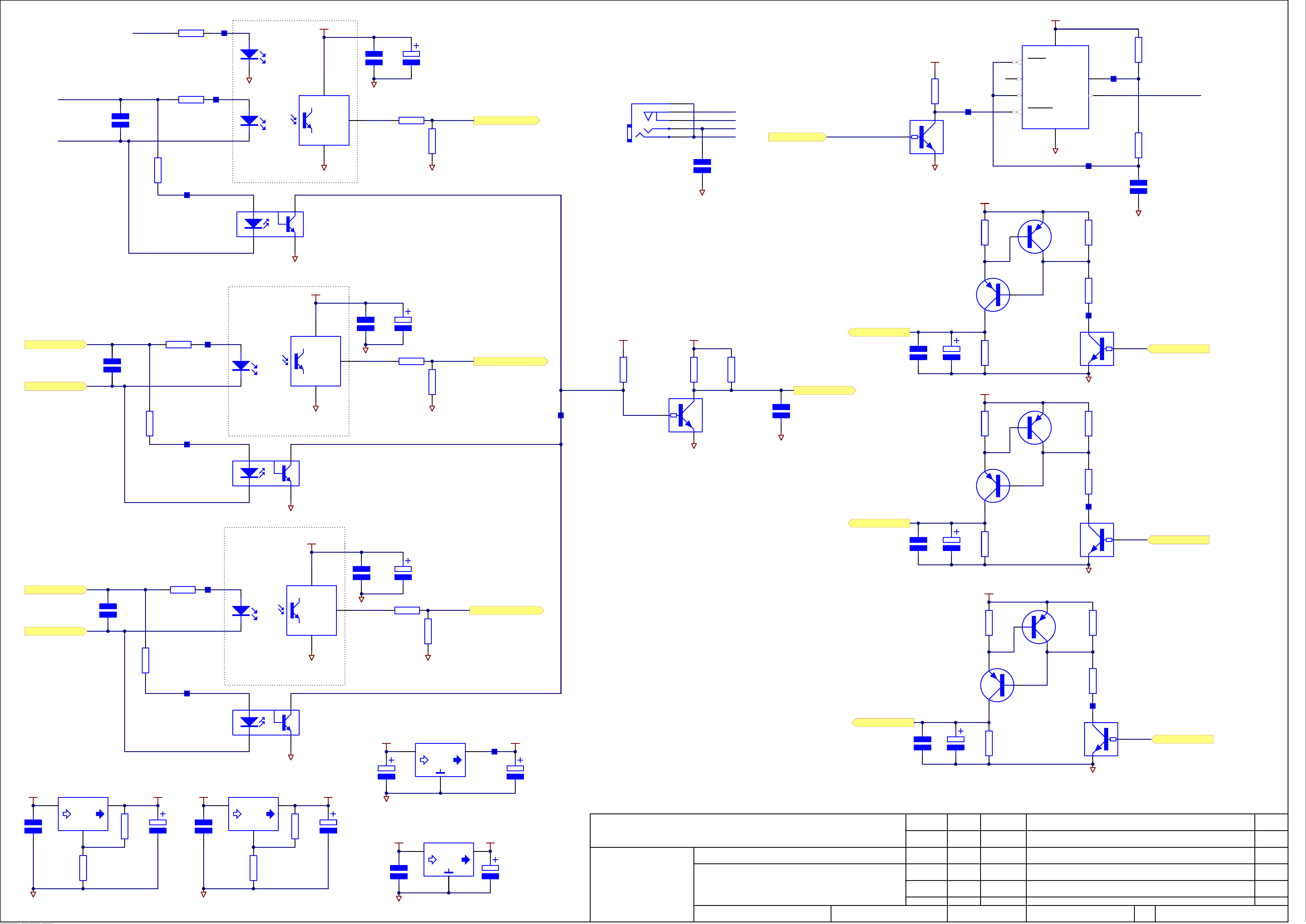
Z1 IR In
Z1 IR Gnd
Z1 LED
C204
220P
50V
R232
150R
0W25
0W063
R206
330R
0W063
R209
750R
0W063
P218
P204
P202
DGND
13
Place LED under IR Rx
+5V_STBY
LED200
SM
RED
RX200
KSM-902TM1N
LED203
SM
RED
+5V
O/P
GND
DGND
64
DGND
C201
100N
16V
X7R
R205
10K
0W063
C220
10UF
50V
YK
Z1 Demod Out
R208
22K
0W063
DGND
Z1 Demod Out
Z1 IR In
SKT200
L
R
WTJ-035-16CB
1
5
4
3
2
Z1 Remod
Z1 LED
Z1 IR In
Z1 IR Gnd
DGND
C223
22P
50V
NPO
IR In
IR In
+5V_STBY
R200
10K
0W063
TR200
MMUN2211LT1
DGND
P200
+12V_IR
+5V_STBY
8
2
5
6
4
TRIG
Vcont
THR HLD
RESET
1
VCC
D CHG
OP
GND
IC200
LMC555CM
P205
7
3
DGND
P201
Astable f=37.1kHz, 40:60 L:H duty cycle
R233
6K8
0W063
Z1 Remod
R201
16K
0W063
C200
1N0
50V
X7R
Z2 IR In
Z2 IR In Gnd
Z2 IR In
C207
220P
50V
R216
330R
0W063
P208
OPTO200
TLP181
DGND
Place LED under IR Rx
+5V_STBY
LED201
SM
RED
+5V
O/P
GND
DGND
C206
100N
X7R
16V
C221
10UF
50V
YK
R218
10K
0W063
Z2 Demod Out
R219
22K
0W063
Z2 Demod Out
+5V_1
R215
4K7
0W063
+12V_IR
R212
2K2
0W125
R227
2K2
0W125
IR Out
IR Out
Z1 Trig Out
Z1 Trig Out
C203
1N0
50V
X7R
C202
10UF
50V
YK
+12V_IR
R202
10R
0W063
0W063
R207
10K
0W063
TR202
BD180
TO-126
TR201
BC859B
SOT-23
R203
4K7
0W063
R204
4K7
0W063
P206
DGND
DGND
TR203
MMUN2211LT1
/Z1 Trig
Z1 Trig
Z3 IR In
Z3 IR In Gnd
Z3 IR In
C209
220P
50V
R210
750R
0W063
P219
Z2 IR In Gnd
0W063
R220
330R
0W063
P214
DGND
RX201
KSM-902TM1N
13
64
OPTO201
TLP181
DGND
Place LED under IR Rx
+5V_STBY
LED202
SM
RED
+5V
O/P
GND
DGND
C219
100N
16V
X7R
R224
10K
0W063
DGND
C222
10UF
50V
YK
Z3 Demod Out
R225
22K
0W063
Z3 Demod Out
P217
DGND
TR207
MMUN2211LT1
DGND
C205
100P
50V
Z2 Trig Out
Z2 Trig Out
C210
1N0
50V
X7R
C208
10UF
50V
YK
R213
10R
0W063
R221
10K
0W063
+12V_IR
R228
10R
0W063
TR205
BD180
TO-126
TR204
BC859B
SOT-23
TR208
BC859B
SOT-23
R214
4K7
0W063
R217
4K7
0W063
P212
DGND
R229
4K7
0W063
TR206
MMUN2211LT1
/Z2 Trig
Z2 Trig
C215
100N
50V
65mA (0.39W)
LM317T
REG202
ADJ
+9V_FM+15V
R222
240R
0W063
R211
750R
0W063
Z3 IR In Gnd
C216
470UF
25V
P221
325mA (0.65W)
LM317T
REG203
C218
100N
50V
13
ADJ
DGND
RX202
KSM-902TM1N
64
OPTO202
TLP181
DGND
R234
240R
0W063
TR209
BD180
TO-126
R230
4K7
0W063
P203
DGND
TR210
MMUN2211LT1
/Z3 Trig
Z3 Trig
C213
10UF
50V
SM
DGND
20mA (0.034W)
LM1117MPX-3.3/NOPB
REG201
+3V3
+3V3_STBY+5V_STBY
P220
C214
470UF
10V
CK
Z3 Trig Out
Z3 Trig Out
C225
1N0
50V
X7R
C224
10UF
50V
YK
R231
10K
0W063
+3V3D+5V_1
DGND
C217
470UF
25V
210mA (0.63W)
L7812CV
REG200
DRAWING TITLE
E.0None on this sheetPK 11/03/0808_E128
Trig / IR / RS232 - IR Demod
+12V_IR+15V
D.0None on this sheetNC 23/01/0808_E016
DGND
R223
1K5
0W25
DGND
R226
390R
0W25
DGND
C212
1uF
25V
X7R
+12
C211
470UF
16V
YXF
ARCAM
A & R Cambridge Ltd.
Pembroke Avenue
Waterbeach
Cambridge CB5 9QR
Filename:
Notes:
Contact Engineer:
L118_C2_IR Demod Trig Drive_E0.SchDoc
Contact Tel: (01223) 203270 tel NoNick Clarke
07_E128
07_E009
ECO No.
INITIALS
Printed:
25/10/06
DATE
03/07/2008
DESCRIPTION OF CHANGE
23Sheet of
A3
DRAWING NO.
C.0PK 15/08/07 None to this sheet07_E213
B.0PK 02/03/07 Updated 9 way D type footprint
A.0.2INITIAL RELEASENC
ISSUE
L118CT
Page 41

+5V_1
DAB/Sirius L In
DGND
R311
10K
0W063
R316
10K
0W063
C307
100P
50V
C309
100P
50V
R314
10K
0W063
AGND
P301
R318
10K
0W063
P300
3
2
84
-5V
DGND
1
DGND
C306
100N
16V
IC301A
NJM2114M
C310
100N
16V
C324
100UF
25V
DAB/Sirius R In
DAB/Sirius L
DGND
R312
10K
0W063
R317
10K
0W063
P304
C308
100P
50V
C311
100P
50V
R315
10K
0W063
AGND
P302
R319
10K
0W063
IC301B
5
6
NJM2114M
C325
7
100UF
25V
DAB/Sirius R
AM/FM L In
R300
2K7
0W063
C300
22UF
63V
6
DGND
2
C301
2N7
50V
FL300
Sagami / XYM-2AA
3
1 4
DGND
R321
10K
0W063
R326
10K
0W063
P305
P307
C313
100P
50V
C316
100P
50V
R324
10K
0W063
AGND
R328
10K
0W063
+5V_1
C312
100N
16V
DGND
84
3
2
-5V
IC302A
NJM2114M
1
C318
100N
16V
C326
AM/FM L
100UF
25V
+5V_1
R330
0R0
0W063
P303
C320
22UF
63V
IC303
1
2
3
4
FC
CAP+
GND
CAP-
SP6661EN-L
C315
100N
16V
C319
22UF
63V
V+
OSC
LV
VOUT
+5V_1
8
7
6
5
-5V
C321
22UF
63V
AM/FM R In
R301
2K7
0W063
C302
22UF
63V
6
DGND
2
C303
2N7
50V
FL301
Sagami / XYM-2AA
3
1 4
DGND
DRAWING TITLE
ARCAM
R322
10K
0W063
R327
10K
0W063
P306
C314
100P
50V
P308
C317
100P
50V
R325
10K
0W063
AGND
R329
10K
0W063
IC302B
5
6
NJM2114M
Ground Balancing
Filename:
Notes:
L118_C3_GND balancing_E0.SchDoc
DGND
7
C327
100UF
25V
AM/FM R
07_E128
E.0Pilot tone filter added to AM/FM ground balancing circuitPK 11/03/0808_E128
D.0None on this sheetNC 23/01/0808_E016
C.0PK 15/08/07 None to this sheet07_E213
B.0PK 02/03/07 Updated 9 way D type footprint
DGND
A & R Cambridge Ltd.
Pembroke Avenue
Waterbeach
Cambridge CB25 9QR
Contact Engineer:
07_E009 NC 25/10/06
ECO No.
Contact Tel: (01223) 203270 tel NoNick Clarke
INITIALS
Printed:
DATE
03/07/2008
DESCRIPTION OF CHANGE
33Sheet of
A3
DRAWING NO.
L118CT
A.0.2INITIAL RELEASE
ISSUE
Page 42

/WL REG
WL IRQ
WL RESET
USB VBUS
USB DRV
R122
47K
0W063
DGND
R121
10K
0W063
Memory
L119_C2_Memory_G0.schdoc
/WL REG
WL IRQ
WL RESET
+5V_1
R101
47K
0W063
P106
TR100
BC846BW
P104
M100
FDN340P
P105
FS100
T750mA
C103
100N
16V
X7R
ETH /RESET
120R@100MHz
L100
C102
100UF
25V
DGND
Ethernet
L119_C4_Ethernet_G0.schdoc
ETH /RESET
CON104
Tyco
292303
56
1
USB DUSB D+
2
3
4
L101
120R@100MHz
DGND
C100
33P
0603
NPO
50V
R123
390K
0W063
X100
24.576MHz
HC-49 SM
NET WClk
NET BClk
NET MClk
NET Data0
Mute
NET L
NET R
R104 10K
R103 10K
R102 10K
DGNDDGND
R106 10K
R105 10K
Audio
L119_C5_Audio_G0.schdoc
R108 10K
R107 10K
R127
470R
0W063
P138
C101
33P
0603
NPO
50V
NET WClk
NET BClk
NET MClk
NET Data0
Mute
NET L
NET R
DEV. USE - NF FOR PRODUCTION
CON101
AMP
+3V3D
0W063
0W063
0W063
0W063
0W063
0W063
0W063
0W063
R109 10K
P135
1
2
3
4
DGND
P163
CON102
P124
1
2
3
4
NET UART0 Tx
NET UART0 Rx
NET Tx
NET Rx
NET MISO
NET MOSI
NET SPI Clk
NET /CS
DGND
NET Xtal In
P134
NET /RESET
+3V3D
R100
1K0
0W063
NET MClk
AMP
+3V3D
R120
47K
0W063
10K
R124
47K
0W063
Power
L119_C6_Power_G0.schdoc
NET Mclk
+3V3D
10K
10K
10K
R161
R162
R163
P158
P159
R164
146
147
141
143
142
193
194
184
185
203
204
190
187
148
149
186
0W063
0W063
0W063
0W063
63
65
79
80
84
85
93
94
67
30
90
92
91
DM850
IC102D
RXD0
TXD0
RXD1
TXD1
TMS
TCK
TDI
TDO
SPIMISO
SPIMOSI
SPICLK
SPINCS0
SPINCS1
SYNC,AV0CTRL2
VCO0
PDOUT0
VCO1
PDOUT1
XTALI
XTALO
PERIPHERALS
CLKOUT
NC1
NC2
/RESET
/TEST2
/TEST3
/TEST4
TEST5
TEST1
47K
47K
RP103D
5 4
RP105D
54
AV0DATA0
AV0DATA1
AV0DATA2
AV0DATA3
AV0CLK
AV0CTRL0
AV0CTRL1
AV1DATA0
AV1DATA1
AV1DATA2
AV1DATA3
AV2DATA0
AV2DATA1
AV2DATA2
AV2CLK
AV2CTRL0
AV2CTRL1
AV3DATA0
AV3DATA1
AV3DATA2
AV3DATA3,/CS3
AV3CLK
AV3CTRL0,A22
AV3CTRL1,A23
AV4DATA0
AV4DATA1
AV4DATA2
AV4DATA3
AV4CLK
AV4CTRL0
AV4CTRL1
4
5
6
7
2
196
197
161
162
163
164
12
13
14
198
199
200
39
40
44
46
33
34
35
21
22
23
24
195
167
168
P120
P121
P122
P123
100R
100R
100R
100R
RP100D
RP100C
2 7
RP100B
1 8
RP100A
R110
R112
R114
RP104A
RP104B
6 3
RP104C
5 4
RP104D
R117 47K
R118
RP105A 47K
RP105B
6 3
RP105C
R126
R128
R129
0W063
0W063
0W063
RP103C
2 7
RP103B
1 8
RP103A
RP102D
RP102C 47K
2 7
RP102B
1 8
RP102A
R133
R134
R135
0W063
0W063
0W063
54
63
56R
56R
56R
18
27
18
27
47K
47K
47K
63
54
63
47K
47K
47K
DGND
P107
0W063
0W063
0W063
47K
47K
47K
47K
47K
0W063
0W063
47K
47K
47K
47K
47K
47K
47K
47K
P108
P109
R116
R125
56R
0W063
NET Data0
NET Data1
NET Data2
NET Data3
P110
47K
47K
47K
47K
RP106D
RP106C
2 7
RP106B
1 8
RP106A
0W063
0W063
0W063
R160
R113
R115
47K
47K
47K
P116
P136
P119
56R
0W063
P100
P101
P103
54
63
DGND
NET BClk
NET WClk
NET MClk
P102
NET SPDIF
NET SPDIF2
NET C vid
NET S-vid C
NET S-vid Y
NET POWER DOWN
NET MODE HOST
NET NIREQ HOST
WL RESET
/WL REG
WL IRQ
R111
0R0
0W063
+5V_1
+6V_1
CON100
1
2
3
4
5
NET SPDIF
6
7
8
9
10
Net C vid
11
12
Net S-vid C
13
14
Net S-vid Y
15
16
NET L
17
18
NET R
19
20
MOLEX
VGND
DGND AGND
CON103
1
VGndDGnd
NET MISO
NET MOSI
2
3
4
5
NET SPI Clk
6
7
NET /CS
8
9
NET MODE HOST
10
11
NET POWER DOWN
12
13
NET /RESET
14
15
NET NIREQ HOST
16
17
NET Rx
18
19
NET Tx
DGND
20
MOLEX
4
4
FIX102
1
FIX100
1
FIX101
1
P144 P145 P146 P147 P148
R141
1
R119
23
0R0
+3V3D
0R0
0W063
R142
10K
0W063
R143
10K
0W063
R144
10K
0W063
1
23
P162
R183
0R0
R184
0R0
DGND
IC102F DM850
USBBUSDRV
USB INTERFACE
USBXTALO
USBD+
USBD-
USBVBUS
USBID
USBREF
USBXTALI
48
49
37
51
52
53
59
60
DGND
P155
P156
P157
R157
1K0
0W063
R156
390R
P161
R159
5K1
USB VBUS R
R158
0R0
0W063
C104
100N
0603
X7R
16V
P137
P154
R155
100R
0W063
P111
TOOL100
TOOL101
TOOL102
TOOL103
USB D+
USB D-
USB DRV
USB VBUS
FID100
FID101
FID102
FID103
DRAWING TITLE
ARCAM
A & R Cambridge Ltd.
Pembroke Avenue
Waterbeach
Cambridge CB5 9QR
DGNDDGND
R145
0R0
0W063
NET - GPIO
Filename:
Notes:
Contact Engineer:
L119_C1_DM850_G0.SchDoc
Contact Tel: (01223) 203270 tel NoNick Clarke
+3V3D
DGND
0W063
0W063
47K
47K
R146
R147
R148
10K
0W063
07_E166
ECO No.
DGND
PK 20/02/0808_E054
PK 07/12/0708_E022
INITIALS
Printed:
0W063
0W063
0W063
0W063
0W063
R136
R137
R138
R139
R140
R149
R150
R151
R153
Mute
15/05/08
DATE
17/07/2008
47K
47K
10K
47K
10K
47K
47K
10K
10K
99
100
101
102
10
P149
P150
P151
0W063
ETH /RESET
0W063
0W063
0W063
P160
Removed CON105 and re-allocated signals
USB socket moved from front input PCB
DESCRIPTION OF CHANGE
P152
P153
16Sheet of
R152
R154
56R
56R
0W063
0W063
P166
11
19
20
9
62
66
64
8
IC102E
USB_D11,GPIO15
USB_D10,GPIO14
USB_D9,GPIO13
USB_D8,GPIO12
USB_D7,GPIO11
USB_D6,GPIO10
USB_D5,GPIO9
USB_D4,GPIO8
USB_CLK,GPIO6
USB_STOP,GPIO3
USB_NEXT,GPIO2
USB_DIR,GPIO1
USB_PCLK,GPIO0
DM850
A3
DRAWING NO.
GPIO PORT/ULPI
G.0PCB mechanics change for GPE panel08_E143 PK 17/07/08
F.0PCB change, make CON101, 102 NF, /Mute changed to Mute08_E129 PK
E.0
D.0UART1 connected to PW338, X100 changed to SMT
C.0Changed power plane through lead connect style to thermal relief,+5V_2>+6V_1PK 25/9/07
ISSUE
L119CT
Page 43

A0
A1
A2
A3
A4
A5
A6
A7
A8
A9
A10
A11
A12
A13,/RAS
A14,/CAS
A15,BA0
A16,BA1
A17,LDQM
A18,UDQM
A19
A20
A21
P202
MEMCLK
MEMCKE
P203
P205
22R
22R
22R
22R
22R
22R
22R
22R
22R
22R
22R
22R
22R
22R
22R
22R
22R
22R
22R
22R
22R
22R
22R
0W063
R216
R218
R220
R222
R224
R226
R228
R230
R232
R234
R236
R238
R240
R242
R244
R246
R247
R248
R249
R250
R251
R252
R254
152
153
154
155
156
159
160
165
166
169
170
171
172
177
178
179
180
181
182
105
106
107
135
117
DM850
IC102B
A0
A1
A2
A3
A4
A5
A6
A7
A8
A9
A10
A11
A12
A13,RAS
A14,CAS
A15,BA0
A16,BA1
A17,DQM0
A18,DQM1
A19
A20
A21
MEMCLK
MEMCKE
MEMORY
D0
D1
D2
D3
D4
D5
D6
D7
D8
D9
D10
D11
D12
D13
D14
D15
/CS0
/CS1
/CS2
/OE
/WE
/WAIT
118
119
120
121
122
123
126
127
130
131
132
133
134
138
139
140
111
110
109
115
108
183
P252
22R
22R
22R
22R
22R
22R
22R
22R
22R
22R
22R
22R
22R
22R
22R
22R
22R
22R
22R
0W063
R217
R219
R221
R223
R225
R227
R229
R231
R233
R235
R237
R239
R241
R243
R245
R202
R209
R253
D0
D1
D2
D3
D4
D5
D6
D7
D8
D9
D10
D11
D12
D13
D14
D15
FLASH /CS
SDRAM /CS
/CS WL
/OE
/WE
/WAIT
FLASH /CS
SDRAM /CS
/CS WL
/OE
/WE
/WAIT
MEMCKE
R201
R203
R205
R204
R208
R206
R207
0W063
0W063
0W063
0W063
0W063
0W063
0W063
+3V3D
4K7
4K7
4K7
4K7
4K7
4K7
4K7
MEMCLK
R200
56R
0W063
P201
DGND
C207
10P
50V
NPO
+3V3D
27
14
1
VDD
MEMCKE D0
MEMCLK
/WE
A14,/CAS
A13,/RAS
SDRAM /CS
A15,BA0
A16,BA1
A11
A10
A9
A8
A7
A6
A5
A4
A3
A2
A1
A0
A17,LDQM
A18,UDQM
P200
37
38
16
17
18
19
20
21
35
22
34
33
32
31
30
29
26
25
24
23
15
39
CKE
CLK
WE*
CAS*
RAS*
CS*
BA0
BA1
A11
A10
A9
A8
A7
A6
A5
A4
A3
A2
A1
A0
LDQM
UDQM
VSS
VDD
VDD
VSS
VSS
3
9
VDDQ
VDDQ
VSSQ
VSSQ
43
49
VDDQ
VDDQ
DQ10
DQ11
DQ12
DQ13
DQ14
DQ15
VSSQ
VSSQ
DQ0
DQ1
DQ2
DQ3
DQ4
DQ5
DQ6
DQ7
DQ8
DQ9
IC200
IC42S16800-6T(G)
2
4
5
7
8
10
11
13
42
44
45
47
48
50
51
53
D1
D2
D3
D4
D5
D6
D7
D8
D9
D10
D11
D12
D13
D14
D15
DGND
C200
100N
16V
X7R
C201
100N
16V
X7R
C202
100N
16V
X7R
C203
100N
16V
X7R
C204
100N
16V
X7R
C205
100N
16V
X7R
+3V3D
C206
100N
16V
X7R
A0
A1
A2
A3
A4
A5
A6
A7
A8
A9
A10
A11
A12
A13,/RAS
/WAIT
/WL REG
WL IRQ
WL RESET
/WL REG
WL IRQ
WL RESET
WiFi module connector
L119_C3_Wifi_G0.SchDoc
A0
A1
A2
A3
A4
A5
A6
A7
A8
A9
A10
A11
A12
A13,/RAS
/WL REG
/WAIT
WL IRQ
WL RESET
D0
D1
D2
D3
D4
D5
D6
D7
D8
D9
D10
D11
D12
D13
D14
D15
/CS WL
/OE
/WE
D0
D1
D2
D3
D4
D5
D6
D7
D8
D9
D10
D11
D12
D13
D14
D15
/CS WL
/OE
/WE
P251
A21
+3V3D +3V3D
R212
4K7
0W063
R213
4K7
0W063
R215
0R0
NF
/RESET_FLASH
/WP
0W063
S29GL064xxxTFIR3x 8M fit R210 & R255, do not fit R211, R214 & R215
AMD29LV641DH 8M fit R211 & R215, do not fit R210, R214 & R255
ST39VF6401B 8M fit R210 & R255, do not fit R211, R214 & R215
A0
A1
A2
A3
A4
A5
A6
A7
A8
A9
A10
A11
A12
A13,/RAS
A14,/CAS
A15,BA0
A16,BA1
A17,LDQM
A18,UDQM
A19
A20
/RESET_FLASH
/WE
/WP
FLASH /CS
/OE
P206
P207
P208
P209
P210
P212
P214
P216
P220
P222
P224
P225
P241
P243
P226
P228
P230
P232
P236
P238
P240
R210
R211
0R0 0W063
0R0
+3V3D
A21
R214
0R0
0W063
R255
0R0
0W063
NF
0W063
P244
P245
P246
P247
P248
P249
NF
25
24
23
22
21
20
19
18
8
7
6
5
4
3
2
1
48
17
16
9
15
10
P250
12
11
14
26
28
13
28
DGND
A0
A1
A2
A3
A4
A5
A6
A7
A8
A9
A10
A11
A12
A13
A14
A15
A16
A17
A18
A19
RY/BY*
A20
RST*
WE*
WP*
CE*
OE*
A21
6
54
41
+3V3D
37
VDD
VSS
46
27
DGND
46
12
47
BYTE*
DQ15/A-1
VSS
52
DQ0
DQ1
DQ2
DQ3
DQ4
DQ5
DQ6
DQ7
DQ8
DQ9
DQ10
DQ11
DQ12
DQ13
DQ14
IC202
S29GL064A90TFIR30
29
31
33
35
38
40
42
44
30
32
34
36
39
41
43
45
D0
D1
D2
D3
D4
D5
D6
D7
D8
D9
D10
D11
D12
D13
D14
D15
+3V3D
DGND
P211
P213
P215
P217
P218
P219
P221
P223
P227
P229
P231
P233
P234
P235
P237
P239
C208
100N
16V
X7R
C209
100N
16V
X7R
DRAWING TITLE
NET - Memory
ARCAM
A & R Cambridge Ltd.
Pembroke Avenue
Waterbeach
Cambridge CB5 9QR
Filename:
Notes:
Contact Engineer:
L119_C2_Memory_G0.SchDoc
Contact Tel: (01223) 203270 tel NoNick Clarke
08_E022
ECO No.
PK 25/9/0707_E166
INITIALS
Printed:
DATE
17/07/2008
DESCRIPTION OF CHANGE
26Sheet of
A3
DRAWING NO.
G.0R255 changed to fitted, PCB mechanics change for GPE panel08_E143 PK 17/07/08
F.0PCB change only08_E129 PK 15/05/08
E.0PK 20/02/0808_E054 None to this sheet
D.0No changes on this sheetPK 07/12/07
C.0Changed power plane through lead connect style to thermal relief
ISSUE
L119CT
Page 44

/CS WL
/OE
/WE
IC300A
1
2
74HC32D
IC300B
4
5
74HC32D
P309
AMP
CON300
/CS WL
P302
/OE WL
/WE WL
DGND
D10
D1
D0
A0
/WL REG
A2
A4
A11
A13,/RAS
/WAIT
A7
A8
A10
D15
D7
D6
D5
D4
47K
0R0
R301
0W063
R300
0W063
/CS WL
+3V3D
P304
NF
P305
P306
3
P300
6
11
13
15
17
19
21
23
25
27
29
31
33
35
37
39
41
43
45
47
49
51
53
55
57
59
61
63
65
67
69
71
73
75
77
79
81
83
85
87
89
91
93
95
97
99
101
103
105
107
109
111
113
115
117
119
121
123
1
TIP
3
8PMJ-3
5
8PMJ-6
7
8PMJ-7
9
8PMJ-8
LED1-P
LED1-N
CHSGND
INTB
3V3
R
GND
CLK
GND
REQ
3V3
AD31
AD29
GND
AD27
AD25
R
C_,_BE3
AD23
GND
AD21
AD19
GND
AD17
C_,_BE2
IRDY
3V3
CLKRUN
SERR
GND
PERR
C_,_BE1
AD14
GND
AD12
AD10
GND
AD8
AD7
3V3
ADS
R
AD3
5V
AD1
GND
SYNC
SD-IN
BIT-CLK
COD-ID1
MOD-A-MON
A-G
S-A-O
S-A-O-G
A-G
R
VCC5VA
GND
GND
GND
GND
RING
8PMJ-1
8PMJ-2
8PMJ-4
8PMJ-5
LED2-P
LED2-N
R
5V
INTA
R
3V3_AUX
RST
3V3
GNT
GND
PME
R
AD30
3V3
AD28
AD26
AD24
IDSEL
GND
AD22
AD20
PAR
AD18
AD16
GND
FRAME
TRDY
STOP
3V3
DEVSEL
GND
AD15
AD13
AD11
GND
AD9
C_,_BE0
3V3
AD6
AD4
AD2
AD0
R_WIP
R_WIP
GND
M66EN
SD-0
C-ID0
RESET
R
GND
S-A-I
S-A-I-G
A-G
MPIACT
3V3_AUX
2
4
6
8
10
12
14
16
18
20
22
24
26
28
30
32
34
36
38
40
42
44
46
48
50
52
54
56
58
60
62
64
66
68
70
72
74
76
78
80
82
84
86
88
90
92
94
96
98
100
102
104
106
108
110
112
114
116
118
120
122
124
+3V3D
P308
P307
/WE WL
R302
R303
0R0
0R0
0W063
0W063
/OE WL
/CS WL
P301
P303
NF
NF
DGND
WL IRQ
WL RESET
D9
D8
A1
A3
A5
A12
A6
D2
D14
A9
D13
D12
D11
D3
DGND
IC300C
9
10
74HC32D
IC300D
12
13
74HC32D
IC300E
VCC
GND
74HC32D
8
11
+3V3D
14
7
DGND
C300
100N
16V
X7R
+3V3D
DGND
C301
100N
16V
X7R
C302
100N
16V
X7R
C303
100N
16V
X7R
C304
100N
16V
X7R
C305
100N
16V
X7R
C306
100N
16V
X7R
C307
100N
16V
X7R
125
126
127
128
DGND
DRAWING TITLE
ARCAM
DGNDDGND
NET - Wifi Connector
Filename:
Notes:
L119_C3_WiFi_G0.SchDoc
G.0PCB mechanics change for GPE panel08_E143 PK 17/07/08
F.0PCB change only08_E129 PK 15/05/08
E.0PK 20/02/0808_E054 None to this sheet
D.0No changes on this sheetPK 07/12/0708_E022
A & R Cambridge Ltd.
Pembroke Avenue
Waterbeach
Cambridge CB5 9QR
Contact Engineer:
C.0Changed power plane through lead connect style to thermal reliefPK 25/9/0707_E166
ECO No.
Contact Tel: (01223) 203270 tel NoNick Clarke
INITIALS
Printed:
DATE
17/07/2008
DESCRIPTION OF CHANGE
36Sheet of
A3
DRAWING NO.
L119CT
ISSUE
Page 45

+3V3D
DGND
R412
R413
R414
R415
0W063
0W063
0W063
0W063
R400
1K5
0W063
47K
47K
47K
47K
MII0
MII1
MII2
MII3
MII17
P400
C400
100N
16V
X7R
120R@100MHz
L400
C401
10uF
10V
X5R
P401
C402
100N
16V
X7R
C403
10uF
10V
X5R
C404
100N
16V
X7R
P402
C405
100N
16V
X7R
DGND
P403
DM850
IC102C
MII INTERFACE
MIIRXD0
MIIRXD1
MIIRXD2
MIIRXD3
MIIRXCLK
MIIRXDV
MIIRXER
MIITXD0
MIITXD1
MIITXD2
MIITXD3
MIITXCLK
MIITXEN
MIITXER
MIICOL
MIICRS
DGND
73
74
75
76
69
70
68
28
27
26
25
41
29
42
98
97
R416
R417
R418
R419
0W063
0W063
0W063
0W063
MII0
MII1
MII2
MII3
MII4
MII5
MII6
MII7
MII8
MII9
MII10
MII11
MII12
MII13
MII14
MII15
47K
47K
47K
47K
P419
P421
P422
P423
P426
P428
P429
P430
P431
P432
P433
P434
P435
P436
P437
P438
MII15
MII6
MII13
MII14
MII0
MII1
MII2
MII3
MII4
MII5
MII6
MII7
MII8
MII9
MII10
MII11
MII12
MII13
MII14
MII15
MII16
MII17
DGND DGND
9
2
AVDDR
AVDDT
AVDDR
DGND
15
29
28
27
26
34
37
38
20
19
18
17
22
21
16
36
35
24
25
32
45
1
RXD0,PHYAD0
RXD1,PHYAD1
RXD2,PHYAD2
RXD3,PHYAD3
RXCLK,10BTSER
RXDV,TESTMODE
RXER,RXD4,RPTR
TXD0
TXD1
CABLESTS,LINKSTS
TXD2
TXD3
TXCLK,ISOLATE
TXEN
TXER,TXD
COL,RMII
CRS,PHYAD4
MDC
MDIO
/MDINTR
NC
AGND5AGND6AGND
46
+3V3D
23
30
41
DVDD
DVDD
DVDD
RX+
BGRES
BGRESG
LEDMODE
LED0,OP0
LED1,OP1
LED2,OP2
DISMDIX
PWRDOWN
/RESET
DGND
DGND
44
33
TX+
TX-
RX-
XT1
XT2
7
8
3
4
48
47
14
+3V3D
31
11
12
13
39
10
40
43
42
DGND
IC400
DM9161A
P414
P416
P420
P424
P425
P427
DGND
R401
51R
0W063
6K2
R409
0W063
R420
0W063
R421
R422
R423
0W063
0W063
0W063
R402
51R
0W063
+3V3D
47K
47K
47K
47K
R403
51R
0W063
R404
51R
0W063
P408
P410
P411
P417
1
2
3
6
7
8
L401
16
15
14
11
10
9
P409
P415
R405
75R
0W063
R407
75R 0W063
0W063
R406
75R
0W063
R408
75R
C406
1N0
2000V
DGND
SCRN1
1
2
3
SCRN2
CON400
Molex
440500001
4
5
6
7
8
SCRN3
SCRN4
MIIMDC
MIIDIO
MIIPHYCLK
82
83
81
MII16
MII17
R410
56R
0W063
P439
P440
P441
ETH /RESET
P442
R411
47K
DGND
DRAWING TITLE
NET - Ethernet
ARCAM
A & R Cambridge Ltd.
Pembroke Avenue
Waterbeach
Cambridge CB5 9QR
Filename:
Notes:
Contact Engineer:
L119_C4_Ethernet_G0.SchDoc
Contact Tel: (01223) 203270 tel NoNick Clarke
08_E022
ECO No.
PK 07/12/07
INITIALS
Printed:
DATE
17/07/2008
DESCRIPTION OF CHANGE
46Sheet of
A3
DRAWING NO.
G.0PCB mechanics change for GPE panel08_E143 PK 17/07/08
F.0PCB change only08_E129 PK 15/05/08
E.0PK 20/02/0808_E054 None to this sheet
D.0CON400 updated for Syspro
C.0Changed power plane through lead connect style to thermal reliefPK 25/9/0707_E166
ISSUE
L119CT
Page 46

C500
NET MClk
NET BClk
NET WClk
NET Data0
DGND DGND
P506
C506
100N
16V
X7R
P512
C511
100N
16V
X7R
+6V_1
D500
LL4148
P533
L500
120R@100MHz
C505
10UF
50V
SM
DGND DGND
4
2
3
1
6
C510
10UF
50V
SM
MCLK
/DEM,SCLK
LRCK
SDIN
FILT+
5
VQ
8
9
VA
AOUTL
AOUTR
GND
P507
IC501
CS4345
7
10
C507
100N
16V
X7R
C517
100UF
SM
P510
P511
R500
2K2
0W063
R506
2K2
0W063
R501
5K1
0W063
R507
5K1
0W063
P500
DGND
P513
DGND
C504
470P
50V
NPO
C514
470P
50V
NPO
P501
P514
P504
C503
10UF
50V
SM
P517
C513
10UF
50V
SM
R504
47K
0W063
+6V_1
R510
47K
0W063
1N0
100V
NPO
5
6
P508
L501
120R@100MHz
C509
1N0
100V
NPO
3
2
DGND
P519
LM358AM
R505
4K7
0W063
C502
470P
50V
NPO
84
LM358AM
R511
4K7
0W063
C515
470P
50V
NPO
7
IC500B
P505
DGND
1
IC500A
P518
L502
120R@100MHz
P526
C519
100N
16V
X7R
L503
120R@100MHz
P502
P515
C518
10UF
SM
C512
10UF
50V
SM
C501
10UF
50V
SM
P503
DGND
P516
DGND
R502
220R
R503
0W063
47K
0W063
R508
220R
R509
0W063
47K
0W063
P532
P531
DGND
DGND
R522
10K
R524
10K
R519
10K
R521
10K
C523
100P
C525
100P
C521
100P
AGND
C527
100P
R523
10K
AGND
R525
10K
R520
10K
R526
10K
P530
P528
P529
5
6
+6V_1
P527
3
2
IC502B
NJM2114M
84
-5V
DGND
DGND
7
C520
100N
IC502A
NJM2114M
1
C526
100N
C522
NET L
100UF
C524
NET R
100UF
Mute
R515
10K
P509
+6V_1
R513
10K
DGND
TR502
BC846BW
P520
R514
1K0
P525
TR500
BC856B
P522
R527
10K
R516
1K0
R518
1K0
P523
P524
DGND
TR503
2SC4548
TR504
2SC4548
-5V
DRAWING TITLE
NET - Audio DAC
Filename:
L119_C5_Audio_G0.SchDoc
DGND
G.0PCB mechanics change for GPE panel08_E143 PK 17/07/08
F.0/Mute changed to Mute08_E129 PK 15/05/08
E.0PK 20/02/0808_E054 None to this sheet
ARCAM
A & R Cambridge Ltd.
Pembroke Avenue
Waterbeach
Cambridge CB5 9QR
Notes:
Contact Engineer:
Changed power plane through lead connect style to thermal relief, +5V_2 > +6V_1
PK 25/9/0707_E166
ECO No.
Contact Tel: (01223) 203270 tel NoNick Clarke
INITIALS
Printed:
DATE
17/07/2008
DESCRIPTION OF CHANGE
56Sheet of
A3
DRAWING NO.
L119CT
D.0No changes on this sheetPK 07/12/0708_E022
C.0
ISSUE
Page 47

+1V8D
10pF caps for plane edge emc
+3V3D
DGND
DGND
C643
10P
C656
10P
C657
10P
C644
10P
C658
10P
C645
10P
C659
10P
C646
10P
DGND
C660
10P
C647
10P
DGND
C623
100N
16V
X7R
DGND
C613
100N
16V
X7R
C661
10P
C648
10P
C602
100N
16V
X7R
C624
100N
16V
X7R
C662
10P
C649
10P
C603
100N
16V
X7R
C614
100N
16V
X7R
C625
100N
16V
X7R
C663
10P
C650
10P
C604
100N
16V
X7R
C615
100N
16V
X7R
C626
100N
16V
X7R
C605
100N
16V
X7R
C616
100N
16V
X7R
C627
100N
16V
X7R
C652
10P
C606
100N
16V
X7R
C617
100N
16V
X7R
C628
100N
16V
X7R
C653
10P
C607
100N
16V
X7R
C618
100N
16V
X7R
C629
100N
16V
X7R
C654
10P
C608
100N
16V
X7R
C619
100N
16V
X7R
C630
100N
16V
X7R
+3V3D
+3V3D
C655
10P
C609
100N
16V
X7R
C620
100N
16V
X7R
C631
100N
16V
X7R
+1V8D
C664
10P
C632
100N
16V
X7R
C665
10P
C667
10P
C668
10P
+3V3D
L600
P601
120R@100MHz
C610
10uF
10V
X5R
C611
100N
16V
X7R
+3V3D
DGND DGND
+1V8D
L601
120R@100MHz
P603
C633
10uF
10V
X5R
P602
L602
120R@100MHz
P604
C634
10uF
10V
X5R
C612
100N
16V
X7R
120R@100MHz
+3V3D
+1V8D
L603
P605
C635
10uF
10V
X5R
16
32
43
61
78
89
103
113
125
136
151
158
176
192
201
55
47
18
38
71
86
95
114
128
144
174
189
56
205
207
3
IC102A
VDDIO
VDDIO
VDDIO
VDDIO
VDDIO
VDDIO
VDDIO
VDDIO
VDDIO
VDDIO
VDDIO
VDDIO
VDDIO
VDDIO
VDDIO
VDDIO
VDDIOUSB
VDDUSB
VDDC
VDDC
VDDC
VDDC
VDDC
VDDC
VDDC
VDDC
VDDC
VDDC
VDDUSBPLL
VDDPLL
VDDDCO
DM850
VSSIOUSB
POWER
VSSUSB
VSUSBPLL
VSSDCO
HEAT PAD
VSSIO
VSSIO
VSSIO
VSSIO
VSSIO
VSSIO
VSSIO
VSSIO
VSSIO
VSSIO
VSSIO
VSSIO
VSSIO
VSSIO
VSSIO
VSSIO
VSSC
VSSC
VSSC
VSSC
VSSC
VSSC
VSSC
VSSC
VSSC
VSSC
VSSPLL
1
15
31
45
58
77
88
104
112
124
137
150
157
175
191
202
54
50
17
36
72
87
96
116
129
145
173
188
57
206
208
209
DGND
R600
0R0
P606
C669
22UF
DGND
IC601
1
2
3
4
FC
CAP+
GND
CAP-
SP6661EN-L
C600
100N
C601
22UF
V+
OSC
LV
VOUT
8
7
6
5
-5V
+6V_1
R614
62R
0W125
DZ600
BZX84C
4V7
DGND
C670
22UF
NET Mclk
10
11
DGND
IC600A
CP
MR
Q10
Q11
74HC4040D
Q0
Q1
Q2
Q3
Q4
Q5
Q6
Q7
Q8
Q9
9
7
6
5
3
2
4
13
12
14
15
1
C636
/32 PSU Sync
P624
100P
50V
NPO
PSU Sync = 768kHz for Mclk = 24.576MHz
PSU Sync = 705.6kHz for Mclk = 22.579MHz
P613
310mA + wifi
REG600
+6V_1 +3V3D
C622
10uF
P615
DGND DGND
R602
130K
R610
100K
DGND
PSU Sync
TPS62050DGSRG4
1
8
6
7
VIN
EN
LBI
SYNC
GND
3
SW
PG
LBO
10
DGND
FB
PGND
9
5
4
2
P623
L604
15uH
R603
1M0
R604
1M0
R605
560K
R611
100K
DGND
C637
6P8
P619P620P621
C621
22uF
DGNDDGNDDGND
L605
P622
15uH
R607
1M0
P618
R608
1M0
P616
680mA
R609
390K
P614
R613
150K
DGND
+1V8D
C641
6P8
REG601
+6V_1
C640
10uF
P617
DGND DGND
R606
130K
R612
100K
DGND
PSU Sync
Blank AVR002 Network PCBL119PBPCB600 1
TPS62050DGSRG4
1
VIN
8
EN
6
LBI
7
SYNC
3
SW
PG
LBO
GND
10
DGND
FB
PGND
9
5
4
2
C638
22uF
+3V3D
VCC
GND
IC600B
74HC4040D
16
8
DGND
C639
100N
DRAWING TITLE
NET - PSU
ARCAM
A & R Cambridge Ltd.
Pembroke Avenue
Waterbeach
Cambridge CB5 9QR
Filename:
Notes:
Contact Engineer:
L119_C6_Power_G0.SchDoc
Contact Tel: (01223) 203270 tel NoNick Clarke
08_E022
ECO No.
PK 07/12/07
PK 25/9/0707_E166
INITIALS
Printed:
DATE
17/07/2008
G.0PCB mechanics change for GPE panel08_E143 PK 17/07/08
F.0PCB change only08_E129 PK 15/05/08
E.0PK 20/02/0808_E054 None to this sheet
Changed power plane through lead connect style to thermal relief, +5V_2 > +6V_1
4v7 supply added to -5V charge pump
DESCRIPTION OF CHANGE
66Sheet of
A3
DRAWING NO.
L119CT
D.0
C.0
ISSUE
Page 48

Main PCB
L121_C2_Main PCB_F0.SchDoc
Vcomp Latch
SPI Clk
SPI Data
AN SPI Data
AN SPI Clk
Zone SPI Clk
Zone SPI Data
DAB SCL
DAB SDA
AN SCL
AN SDA
VidIO Mux Latch
AIn Mux Latch
AOut Mux Latch
IRTrig Mux Latch
NET MISO_D
NET MOSI
NET SPI Clk
NET/CS
NET Mode Host
NET Power Down
NET NIREQ Host
DSP Clk
DSP MISO
DSP MOSI
DSP /CS
DSP2 FLAG0
DSP1 FLAG0
RDS Int
RDS Data
FM Data Out
FM CE
NET /RESET
DSP2 /CS
iPod /Present
SPDIF /Reset
VSM
Vcomp Latch
SPI Clk
SPI Data
AN SPI Data
AN SPI Clk
Zone SPI Clk
Zone SPI Data
DAB SCL
DAB SDA
AN SCL
AN SDA
VidIO Mux Latch
AIn Mux Latch
AOut Mux Latch
IRTrig Mux Latch
NET MISO_D
NET MOSI
NET SPI Clk
NET/CS
NET Mode Host
NET Power Down
NET NIREQ Host
DSP Clk
DSP MISO
DSP MOSI
DSP
/CS
DSP2 FLAG0
DSP1 FLAG0
RDS Int
RDS Data
FM Data Out
FM CE
NET /RESET
DSP2 /CS
iPod /Present
SPDIF /Reset
VSM
Daughter PCBs
L121_C3_Daughter PCBs_F0.SchDoc
Vcomp Latch
SPI Clk
SPI Data
AN SPI Data
AN SPI Clk
Zone SPI Clk
Zone SPI Data
DAB SCL
DAB SDA
AN SCL
AN SDA
VidIO Mux Latch
AIn Mux Latch
AOut Mux Latch
IRTrig Mux Latch
NET MISO_D
NET MOSI
NET SPI Clk
NET/CS
NET Mode Host
NET Power Down
NET NIREQ Host
DSP Clk
DSP MISO
DSP MOSI
DSP /CS
DSP2 FLAG0
DSP1 FLAG0
RDS Int
RDS Data
FM Data Out
FM CE
NET /RESET
DSP2 /CS
iPod /Present
SPDIF /Reset
VSM
FIX106
Dia 3.5mm
FIX107
Dia 3.5mm
FIX108
Dia 3.5mm
FIX109
Dia 3.5mm
1
P105
1
P108
1
P111
1
P114
NF
R100
0R0
0W063
NF
R101
0R0
0W063
NF
R102
0R0
0W063
NF
R103
0R0
0W063
AGND
AGND
AGND
AGND
FIX100
Dia 3.5mm
FIX110
Dia 3.5mm
FIX111
Dia 3.5mm
FIX104
Dia 3.5mm
FIX105
Dia 3.5mm
1
P106
1
P109
1
P112
1
P115
1
P117
NF
R107
0R0
0W063
NF
R104
0R0
0W063
NF NF
R105
0R0
0W063
NF
R111
0R0
0W063
NF
R112
0R0
0W063
DGND
DGND
DGND
DGND
DGND
FIX102
1
P107
Dia 3.5mm
FIX101
1
P110
Dia 3.5mm
FIX112
1
P113
Dia 3.5mm
FIX103
1
P116
Dia 3.5mm
NF
R109
0R0
0W063
NF
R108
0R0
0W063
R106
0R0
0W063
NF
R110
0R0
0W063
VGND
DGND
DGND
VGND
Z1 Demod Out
Z2 Demod Out
Z3 Demod Out
WClk PW338
Headphone Sense
Z2 /Mute
Z3 /Mute
/Main Mute
/Sbl/Sbr Mute
RS232 Tx
RS232 Rx
Y in
Pb In
Pr In
Cvid In
S-vid Y In
S-vid C In
Z1 Demod Out
Z2 Demod Out
Z3 Demod Out
WClk PW338
Headphone Sense
Z2 /Mute
Z3 /Mute
/Main Mute
/Sbl/Sbr Mute
RS232 Tx
RS232 Rx
Y in
Pb In
Pr In
Cvid In
S-Vid Y In
S-Vid C In
Z1 Demod Out
Z2 Demod Out
Z3 Demod Out
WClk PW338
Headphone Sense
Z2 /Mute
Z3 /Mute
/Main Mute
/Sbl/Sbr Mute
RS232 Tx
RS232 Rx
Y in
Pb In
Pr In
Cvid In
S-vid Y In
S-vid C In
PH
CON101
JST
PSU
1
2
3
4
5
6
DGND
Clk PSU
Relay Sw
/AC Present
+5V_STBY
1V8D
DGND
AGND
VGND
CON100
7
8
9
10
11
12
MOLEX
PSU
+3V3_PW338
1
+5V_1
2
+6V_1
3
+40V_VFD
4
+15V
5
6
-15V
NET Cvid
NET S-vid C
NET S-vid Y
NET Tx
NET Rx
Sirius Tx
Sirius Rx
iPod Tx
iPod Rx
Y ADV7312
Pb ADV7312
Pr ADV7312
Cvid Out
S-vid Y Out
S-vid C out
HDMI Data0
HDMI Data1
HDMI Data2
HDMI Data3
HDMI SPDIF
HDMI WClk
HDMI BClk
HDMI MClk
Dig Mux Latch
FP int
FP_TX
FP_RX
SPDIF_Present
NET Cvid
NET
S-vid C
NET S-vid Y
NET Tx
NET Rx
Sirius Tx
Sirius Rx
iPod Tx
iPod Rx
Y ADV7312
Pb ADV7312
Pr ADV7312
Cvid Out
S-vid Y Out
S-vid C Out
HDMI Data0
HDMI Data1
HDMI Data2
HDMI Data3
HDMI SPDIF
HDMI WClk
HDMI BClk
HDMI MClk
Dig Mux Latch
FP int
FP_TX
FP_RX
SPDIF_Present
NET Cvid
NET S-vid C
NET S-vid Y
NET Tx
NET Rx
Sirius Tx
Sirius Rx
iPod Tx
iPod Rx
Y ADV7312
Pb ADV7312
Pr ADV7312
Cvid Out
S-vid Y Out
S-vid C out
HDMI Data0
HDMI Data1
HDMI Data2
HDMI Data3
HDMI SPDIF
HDMI WClk
HDMI BClk
HDMI MClk
Dig Mux Latch
FP Int
FP_TX
FP_RX
SPDIF_Present
Clk PSU
Clk PSU
Amp
CON102
MOLEX
52806
1
2
3
4
5
6
7
8
DGND
P100
P101
P102
P103
P104
FAN PWM
Amp Fault
Amp Temp1
Amp Temp2
Amp Temp3
TOOL100 TOOL101 TOOL102 TOOL103
FD100FD101FD102FD103
/AC Present
Relay Sw
FAN PWM
Amp Temp1
Amp Temp2
Amp Temp3
Amp Fault
/AC Present
Relay Sw
FAN PWM
Amp Temp1
Amp Temp2
Amp Temp3
Amp Fault
DRAWING TITLE
Connection PCB
ARCAM
A & R Cambridge Ltd.
Pembroke Avenue
Waterbeach
Cambridge CB5 9QR
Filename:
Notes:
Contact Engineer:
Blank AVR002 Connection PCBL121PBPCB100 1
L121_C1_Motherboard_F0.SchDoc
Contact Tel: (01223) 203270 tel NoNick Clarke
08_E017
07_E126
ECO No.
INITIALS
Printed:
DATE
03/07/2008
CON317 connections altered, HDMI Clks added08_E035 08/02/08
Changed power plane connect style to direct, iPod removed, +5V_2 > +6V_1 B.0PK 02/03/07
DESCRIPTION OF CHANGE
13Sheet of
A3
DRAWING NO.
F.0PCB change only08_E130 PK 15/05/08
E.0PK 20/02/0808_E055 None to this sheet
D.0NC
C.0PK 02/08/07 Rename DSP signals for AD DSP, correct backwards bottom silk
ISSUE
L121CT
Page 49

+3V3_PW338
+3V3_PW338 +5V_1+5V_STBY
1V8D
Z3 /Mute
Z2 /Mute
/Sbl/Sbr Mute
/Main Mute
SPDIF /Reset
NET /RESET
DSP2 /CS
NET MISO_D
NET Power Down
FP_RX
DAB SDA
SPI Clk
SPI Data
AN SPI Data
RDS Int
iPod /Present
FM CE
AOut Mux Latch
Relay Sw
NET MOSI
NET SPI Clk
NET Mode Host
DSP MOSI
DSP /CS
DSP1 FLAG0
Headphone Sense
CON200
12
34
56
78
910
1112
1314
1516
1718
1920
2122
2324
2526
2728
2930
3132
3334
3536
3738
3940
4142
4344
4546
4748
4950
5152
5354
5556
5758
5960
6162
6364
6566
6768
6970
7172
7374
7576
7778
7980
8182
8384
8586
8788
8990
9192
9394
9596
9798
99100
101102
103104
105106
107108
109110
111112
113114
115116
117118
119120
Hirose
FX8C-120P-SV
SPDIF_Present
FAN PWM
FP_TX
DAB SCL
Zone SPI Data
AN SCL
AN SDA
AN SPI Clk
Zone SPI Clk
FM Data Out
RDS Data
WClk PW338
Was I2S mux
Vcomp Latch
VidIO Mux Latch
AIn Mux Latch
IRTrig Mux Latch
Dig Mux Latch
NET/CS
Amp Temp1
Amp Temp2
Amp Temp3
NET NIREQ Host
FP int
DSP MISO
DSP Clk
Y ADV7312
Pb ADV7312
Pr ADV7312
S-vid Y Out
S-vid C out
Cvid Out
HDMI MClk
HDMI BClk
Was iPod SVid Y
Was iPod CVid
Y in
S-vid Y In
NET S-vid C
Pr In
CON201
12
34
56
78
910
1112
1314
1516
1718
1920
2122
2324
2526
2728
2930
3132
3334
3536
3738
3940
4142
4344
4546
4748
4950
5152
5354
5556
5758
5960
6162
6364
6566
6768
6970
7172
7374
7576
7778
7980
8182
8384
8586
8788
8990
9192
9394
9596
9798
99100
101102
103104
105106
107108
109110
111112
113114
115116
117118
119120
Hirose
FX8C-120P-SV
DSP2 FLAG0
Amp Fault
VSM
RS232 Tx
Z2 Demod Out
Z1 Demod Out
Z3 Demod Out
RS232 Rx
/AC Present
HDMI SPDIF
Sirius Rx
NET Rx
iPod Rx
iPod Tx
NET Tx
Sirius Tx
HDMI WClk
HDMI Data3
HDMI Data2
HDMI Data1
HDMI Data0
NET S-vid Y
Pb In
Cvid In
Was iPod SVid C
NET Cvid
S-vid C In
DRAWING TITLE
DGNDDGNDDGNDDGND VGND
Main PCB Connectors
VGND
F.0PCB change only08_E130 PK 15/05/08
E.0PK 20/02/0808_E055 None to this sheet
ARCAM
A & R Cambridge Ltd.
Pembroke Avenue
Waterbeach
Cambridge CB5 9QR
Filename:
Notes:
Contact Engineer:
L121_C2_Main PCB_F0.SchDoc
Contact Tel: (01223) 203270 tel NoNick Clarke
07_E126
ECO No.
INITIALS
Printed:
DATE
03/07/2008
CON317 connections altered, HDMI Clks added08_E035 08/02/08
Changed power plane connect style to direct, iPod audio/video removed B.0PK 02/03/07
DESCRIPTION OF CHANGE
23Sheet of
A3
DRAWING NO.
D.0NC
C.0PK 02/08/07 Rename DSP signals for AD DSP, correct backwards bottom silk08_E017
ISSUE
L121CT
Page 50

CON312
SAMTEC
SSQ
CON318
COMPONENT IO
SAMTEC
SSQ
+5V_1 +15V
1
2
3
4
5
6
SPI Clk
7
8
SPI Data
9
10
11
12
13
14
15
16
17
18
19
20
VGNDDGND
1
2
3
4
5
6
7
8
9
10
11
12
13
14
15
16
17
18
19
20
VGND AGND
Z3 L
Z3 R
-15V
Vcomp Latch
Y ADV7312
Pb ADV7312
Pr ADV7312
Y in
Pb In
Pr In
CON300
SAMTEC
SSQ
CON306
VIDEO IO
SAMTEC
SSQ
1
2
3
4
5
6
7
8
9
10
11
12
13
14
15
16
17
18
19
20
VGND
1
2
3
4
5
6
7
8
9
10
11
12
13
14
15
16
17
18
19
20
DGND
AGND
+15V
-15V
+5V_1
Z2 R
Z2 L
SPI Data
SPI Clk
Z3 L
Z3 R
Cvid Out
S-vid C out
S-vid Y Out
Cvid In
S-vid Y In
S-vid C In
VidIO Mux Latch
SPI Data
SPI Clk
AGND
Zone SPI Clk
Zone SPI Data
Z2 /Mute
Z3 /Mute
CON313
SAMTEC
SSQ
DSP
CON319
SAMTEC
SSQ
1
2
3
4
5
6
7
8
9
10
11
12
13
14
15
16
17
18
19
20
DGND
1
2
3
4
5
6
7
8
9
10
11
12
13
14
15
16
17
18
19
20
DGND
+6V_1
DSP BClk
DSP MClk
DSP WClk
DSP BClk Out
DSP WClk Out
I2S Data
Data LR
Data CSw
Data SlSr
Data SblSbr
DIGITAL IO
SAMTEC
SSQ
DSP2 /CS
DSP Clk
DSP MISO
DSP MOSI
DSP /CS
DSP1 FLAG0
DSP2 FLAG0
HDMI Data0
HDMI Data2
HDMI Data1
HDMI Data3
CON301
SAMTEC
SSQ
CON307
1
2
3
4
5
6
7
8
9
10
11
12
13
14
15
16
17
18
19
20
DGND
1
2
3
4
5
6
7
8
9
10
11
12
13
14
15
16
17
18
19
20
DGND
SPDIF_Present
SPDIF /Reset
Was Net WCLK
NET SPDIF
HDMI BClk
HDMI WClk
HDMI MClk
HDMI SPDIF
AUX SPDIF
Was DAB/Sirius SPDIF
AN SDA
AN SCL
MClk
BClk
WClk
I2S Data
ADC Data
AN SDA
AN SCL
+5V_1
AN SPI Data
AN SPI Clk
Dig Mux Latch
CON302
SAMTEC
SSQ
CON308
Analogue Input
SAMTEC
SSQ
CON314
SAMTEC
SSQ
1
2
3
4
5
6
7
8
9
10
11
12
13
14
15
16
17
18
19
20
AGND
1
2
3
4
5
6
7
8
9
10
11
12
13
14
15
16
17
18
19
20
AGND
1
2
3
4
5
6
7
8
9
10
11
12
13
14
15
16
17
18
19
20
DGND
Z2 L
Z2 R
AUX L
AUX R
Was iPod L
Was iPod R
DAB/Sirius L
DAB/Sirius R
NET L
NET R
Phono L
Phono R
AM/FM L
AM/FM R
Main L
Main R
+15V
-15V
ADC WClk
ADC BClk
ADC MClk
ADC Data
AN SPI Data
AN SPI Clk
AN SCL
AN SDA
AN SPI Data
AN SPI Clk
AIn Mux Latch
CON320
FRONT INPUT
MOLEX
52045
Analogue Output
1
2
3
4
5
6
7
8
9
10
11
12
13
14
15
16
DGND
CON303
SAMTEC
SSQ
CON309
SAMTEC
SSQ
AGND
Headphone R
Headphone L
AUX R
AUX L
AUX SPDIF
+5V_1
1
2
3
+15V
-15V
Phono L
4
5
Phono R
6
Headphone L
7
8
Headphone R
9
10
11
Z2 L
12
13
Z2 R
14
15
Main L
16
17
Main R
18
19
20
AGND
1
DAC WClk
2
3
DAC MClk
4
5
DAC BClk
6
7
Data LR
8
9
Data CSw
10
11
Data SlSr
12
AN SCL
13
Data SblSbr
14
AN SPI Data
15
AN SDA
16
17
AN SPI Clk
18
19
20
DGND
Headphone Sense
/Main Mute
AOut Mux Latch
/Sbl/Sbr Mute
CON317
+40V_VFD
1
2
3
4
5
6
7
8
FRONT PANEL
9
10
MOLEX
52045
CON FFC V 1.25MM 10W
DGND
CON304
SAMTEC
SSQ
CON310
IR/TRIG/RS232
SAMTEC
SSQ
CON315
SAMTEC
SSQ
+6V_1
IR In
+3V3_PW338
1
2
3
4
5
6
7
8
9
10
11
12
13
14
15
16
17
18
19
20
AGND
1
2
3
4
5
6
7
8
9
10
11
12
13
14
15
16
17
18
19
20
DGND
1
2
3
4
5
6
7
8
9
10
11
12
13
14
15
16
17
18
19
20
DGND
+5V_STBY
FP Int
FP_TX
FP_RX
Was iPod L
Was iPod R
AM/FM L
AM/FM R
DAB/Sirius L
DAB/Sirius R
Was VGnd
Was iPod SVid Y
Was VGnd
Was iPod SVid C
Was VGnd
Was iPod CVid
iPod /Present
VSM
RDS Int
RDS Data
FM Data Out
SPI Clk
SPI Data
FM CE
DAB SCL
DAB SDA
+5V_STBY
+5V_1
RS232 Tx
RS232 Rx
Sirius Tx
Sirius Rx
iPod Tx
iPod Rx
Z2 Demod Out
IR In
Z1 Demod Out
Z3 Demod Out
IRTrig Mux Latch
Was DAB/Sirius SPDIF
+15V
CON305
SAMTEC
SSQ
CON311
NETWORK
SAMTEC
SSQ
1
2
3
4
5
6
7
8
9
10
11
12
13
14
15
16
17
18
19
20
1
2
3
4
5
6
7
8
9
10
11
12
13
14
15
16
17
18
19
20
+6V_1
+5V_1
AGNDDGND
DGND
NET SPDIF
NET Cvid
NET S-vid C
NET S-vid Y
NET L
NET R
VGNDDGND
NET MISO_D
NET MOSI
NET SPI Clk
NET/CS
NET Mode Host
NET Power Down
NET /RESET
NET NIREQ Host
NET Rx
NET Tx
IC300A
1
OE
WClk
DSP WClk Out DSP BClk Out
DGND
+3V3_PW338
19
17
15
13
11
DGND
2
4
6
8
74HC244D
IC300B
74HC244D
A0
A1
A2
A3
OE
A0
A1
A2
A3
Y0
Y1
Y2
Y3
Y0
Y1
Y2
Y3
18
16
14
12
3
5
7
9
P309
P310
P311
P313
62mW
62mW
62mW
62mW
100R
100R
100R
100R
RP300A
RP300B
6 3
RP300C
5 4
RP300D
18
27
ADC WClk
DSP WClk
P312
WClk PW338
BClk
MClk
DGND
DGND
DGND
19
17
15
13
11
IC301A
1
OE
2
A0
4
A1
6
A2
8
A3
74HC244D
IC301B
OE
A0
A1
A2
A3
74HC244D
Y0
Y1
Y2
Y3
Y0
Y1
Y2
Y3
18
16
14
12
3
5
7
9
100R
100R
100R
100R
62mW
62mW
62mW
P300
P301
P302
P304
5 4
P305
6 3
P306
P307 P308
62mW
RP301A
RP301B
6 3
RP301C
5 4
RP301D
100R
100R
100R
100R
62mW
62mW
62mW
62mW
RP302D
RP302C
RP302B
RP302A
27
18
18
27
ADC MClk
DSP MClk
DAC MClk
ADC BClk
DSP BClk
DAC BClkDAC WClk
DGND
IC303A
10
11
74HC4040D
CP
MR
Q0
Q1
Q2
Q3
Q4
Q5
Q6
Q7
Q8
Q9
Q10
Q11
9
7
6
5
3
2
4
13
12
14
15
1
P303
/64
R300
100R
0W063
Clk PSU
352.8kHz for 44.1,88.2,176.4kHz
384kHz for 32, 48,96,192kHz
+3V3_PW338
VCC
GND
74HC244D
IC300C
20
10
DGND
C300
100N
16V
+3V3_PW338
VCC
GND
74HC244D
IC301C
20
10
DGND
C302
100N
16V
+3V3_PW338
VCC
GND
74HC4040D
IC303B
16
8
DGND
C303
100N
16V
+3V3_PW338
C304
10uF
10V
DGND
DRAWING TITLE
Daughter PCB Connectors
ARCAM
A & R Cambridge Ltd.
Pembroke Avenue
Waterbeach
Cambridge CB5 9QR
Filename:
Notes:
Contact Engineer:
L121_C3_Daughter PCBs_F0.SchDoc
Contact Tel: (01223) 203270 tel NoNick Clarke
08_E035 08/02/08
07_E126
ECO No.
INITIALS
Printed:
DATE
03/07/2008
CON316 removed signals reallocated to CON305
CON320 changed to 16 way as USB removed from front input
Changed power plane connect style to direct, iPod removed, +5V_2 > +6V_1 B.0PK 02/03/07
DESCRIPTION OF CHANGE
33Sheet of
DRAWING NO.
A2
F.0PCB change only08_E130 PK 15/05/08
E.0PK 20/02/0808_E055
D.0NC CON317 connections altered, HDMI Clks added
C.0PK 02/08/07 Rename DSP signals for AD DSP, correct backwards bottom silk08_E017
ISSUE
L121CT
Page 51

Blank AVR002 HDMI PCBL122PBPCB100 1
PW338 Analogue Input Port
L122_C3_PW338_Analogue_Input_Port_F0.SchDoc
Cvid In
S-Vid C In
S-Vid Y In
NET S-vid C
NET S-vid Y
NET Cvid
Pr In
Pb In
Y In
Motherboard Connections
L122_C11_Motherboard_Connections_F0.SchDoc
Cvid In
S-vid C In
S-vid Y In
NET S-vid C
NET S-vid Y
NET Cvid
Pr In
Pb In
Y in
PW338 Digital Input Port
L122_C2_PW338_Digital_Input_Port_F0.SchDoc
AOut Mux Latch
IRTrig Mux Latch
AOut Mux Latch
Dig Mux Latch
Dig Mux Latch
IRTrig Mux Latch
VidIO Mux Latch
VComp Latch
Vcomp Latch
VidIO Mux Latch
DSP CLK
DSP Clk
DSP MOSI
DSP MOSI
DSP MISO
DSP MISO
DSP /CS
DSP /CS
DSP2 FLAG0
DSP1 FLAG0
DSP2 FLAG0
DSP1 FLAG0
AIn Mux Latch
AIn Mux Latch
NET SPI Clk
NET SPI Clk
NET MOSI
NET MOSI
NET MISO_D
NET MISO_D
NET /CS
NET /CS
PW338 Peripherals
L122_C7_PW338_Peripherals_F0.SchDoc
HDMIRx Sync
SiI9135 /RESET
HDMIRx Int
HDMIRx Mute
HDMI_config_sda
HDMI_config_scl
NET NIREQ Host
Net Power Down
Net Mode Host
HDMI Data0
HDMI Data1
HDMI Data2
HDMI Data3
HDMI SPDIF
HDMI MClk
HDMI BClk
HDMI WClk
FP Int
Headphone Sense
Amp Fault
595A Latch
595BC Latch
RS232 Tx
RS232 Rx
FP int
FP TX
FP RX
Amp Fault
HDMI Data1
HDMI Data0
NET Mode Host
NET NIREQ Host
NET Power Down
HDMI Data3
HDMI Data2
HDMI SPDIF
HDMI MCLK
HDMI BCLK
HDMI WCLK
Headphone Sense
AN_SDA
AN_SCL
DAB_SDA
DAB_SCL
SPDIF /Reset
DSP2 /CS
NET /RESET
HDMIRx Sync
SiI9135 /RESET
HDMIRx Int
HDMIRx Mute
HDMI_config_sda
HDMI_config_scl
595A Latch
595BC Latch
RS232 Tx
RS232 Rx
FP Tx
FP Rx
AN_SDA
AN_SCL
DAB_SDA
DAB_SCL
SPDIF /RESET
DSP2 /CS
NET /RESET
PW338 Hotplug
HDMI_DDCSelAV
HDMI_DDCSelSAT
HDMI_DDCSelDVD
HDMI_DDCSelVCR
HDMI_DDCSelPVR
HDMI_TMDSSel0
HDMI_TMDSSel1
HDMI_TMDSSel2
HDMI_TMDSSel3
IP_DDCSel0
IP_DDCSel1
IP_DDCSel2
EDID_SCL
EDID_SDA
EDID_Sel
Sheet 09 - HDMI Input MUX
L122_C9_HDMI_Input_MUX_F0.SchDoc
PW338 Hotplug
HDMI_DDCSelAV
HDMI_DDCSelSAT
HDMI_DDCSelDVD
HDMI_DDCSelVCR
HDMI_DDCSelPVR
HDMI_TMDSSel0
HDMI_TMDSSel1
HDMI_TMDSSel2
HDMI_TMDSSel3
IP_DDCSel0
IP_DDCSel1
IP_DDCSel2
EDID_SCL
EDID_SDA
EDID_Sel
Display_CEC
TOOL100
TOOL101
TOOL102
TOOL103
FD100 FD101 FD102 FD103
FD104 FD105 FD106 FD107
FD108 FD109
BGA fiducials
FD110
TQFP144 fiducial (with FD108)
FD112 FD113
TQFP100 fiducials
FD114 FD115
TQFP100 fiducials
Top fiducials
Bottom fiducials
PW338 Display Port
L122_C5_PW338_Display_Port_F0.SchDoc
Pb ADV7312
Y ADV7312
Display_CEC
Zone SPI Data
Zone SPI Clk
AN SPI Clk
AN SPI Data
SPI Clk
SPI Data
VSM
RDS Data
FM CE
FM Data Out
i2s mux
SPDIF_Present
Amp_Temp_1
Amp_Temp_2
Amp_Temp_3
Z3 Demod Out
Z2 Demod Out
Z1 Demod Out
iPod /Present
/Sbl/Sbr Mute
Z2 /Mute
Z3 /Mute
/Main Mute
Relay Sw
FAN PWM
iPod Rx
Pr ADV7312
S-vid Y Out
Cvid Out
S-vid C out
WClk PW338
/AC Present
iPod Tx
Sirius Rx
Sirius Tx
NET Tx
NET Rx
RDS Int
Zone SPI Data
Zone SPI Clk
AN SPI Clk
AN SPI Data
SPI Clk
SPI Data
VSM
RDS Data
FM CE
FM Data Out
i2s mux
SPDIF_Present
Amp_Temp_1
Amp_Temp_2
Amp_Temp_3
Z3 Demod Out
Z2 Demod Out
Z1 Demod Out
iPod /Present
/Sbl/Sbr Mute
Z2 /Mute
Z3 /Mute
/Main Mute
Relay Sw
FAN PWM
QUART RESET
Display1_5v_off
Display2_5v_off
RS232 /CSC
iPod_UART_Int
Sirius_UART_Int
NET_UART_Int
ADV7310 /RESET
HDMITx_2 Int
SiI9134_2/RESET
HDMITx_1 Int
SiI9134_1/RESET
Vid_Clk_Sw
HDMI Output MUX
L122_C10_HDMI_Output_MUX_F0.SchDoc
Display1_5v_off
Display2_5v_off
FIX100
1
Dia 3.5mm
FIX101
1
Dia 3.5mm
FIX102
1
Dia 3.5mm
R100
0R0
0W063
R101
0R0
0W063
R102
0R0
0W063
DGnd
DGnd
DGnd
Display_CEC
PW338 Power
L122_C8_PW338_Power_and_Ground_F0.SchDoc
HDMI MClk
HDMI_config_sda
HDMI_config_scl
HDMI SPDIF
PW338 Main Memory
L122_C6_PW338_Main_Memory_Port_F0.SchDoc
CVid Out
S-vid Y Out
Y ADV7312
SiI9135 Power
L122_C12_Sii9135_Power_F0.SchDoc
Pr ADV7312
Pb ADV7312
S-Vid C out
HDMITx_1 Int
Vid_Clk_Sw
SiI9134 Power
L122_C13_Sii9134_Power_F0.SchDoc
SiI9134_1/RESET
FIX103
1
iPod Tx
iPod Rx
/AC Present
WClk PW338
Sirius Tx
Sirius Rx
QUART RESET
NET_UART_Int
Sirius_UART_Int
iPod_UART_Int
ADV7310 /RESET
SiI9134_2/RESET
HDMITx_2 Int
PW338 CPU
L122_C4_PW338_CPU_F0.SchDoc
DRAWING TITLE
RS232 /CSC
NET Tx
NET Rx
RDS Int
Dia 3.5mm
FIX104
1
Dia 3.5mm
R103
0R0
0W063
R104
0R0
0W063
DGnd
DGnd
F.0None to this sheetPK 23/04/0808_E138
Top Level
08_E037
E.0Re-name DSP signals for AD DSP, HDMI Clks routed to L121PK 13/12/07
ARCAM
A & R Cambridge Ltd.
Pembroke Avenue
Waterbeach
Cambridge CB5 9QR
Filename:
Notes:
Contact Engineer:
L122_C1_TopLevel_F0.SchDoc
Contact Tel: (01223) 203200Nick Clarke
ECO No.
NC07_E177 16/10/07
INITIALS
Printed:
DATE
08/07/2008
EDID I2S Bus added, CEC connected to PW338NC 20/11/0707_E205
PCB change onlyNC 26/3/07 B.107_E058
DESCRIPTION OF CHANGE
113Sheet of
A3
DRAWING NO.
D.0
C.0AC Present > /AC Present, HDMI EDID -> DAB I2C, Video doubler
ISSUE
L122CT
Page 52

I2C Addr = 0x60/0x68
C200
22P
C201
DGnd
22P
IC201C
SII9135
R201
4K7
0W063
DGnd
50V
50V
SiI9135
Digital Audio Output Pins
HDMI_config_scl
HDMI_config_sda
R200
1M0
0W063
P222
SM
XTALIN
XTALOUT
MCLK
SCK/DCLK
WS/DR0
SD0/DL0
SD1/DR1
SD2/DL1
SD3/DR2
SPDIF/DL2
MUTEOUT
X200
28.322 MHz
95
94
89
86
85
81
82
83
84
78
75
SiI9135 /RESET
P203
HDMI scl
HDMI sda
P236
P284
P285
P243
P250
P253
P256
SII9135
IC201A
Config/Prog Pins
100
105
27
26
33R
33R
R204
R205
1 8
2 7
2 7
RP201A
1 8
33R
62mW
Spare
0W063
0W063
33R
/RESET
CI2CA
CSCL
CSDA
SiI9135
RSVDL
99
R202
4K7
0W063
DGnd
RP200D
54
RP201D
54
RP200A
RP200B
RP200C
63
RP201C
63
RP201B
RSVDNC
RSVDNC
55
76
NC
NC
P237
P286
P287
P244
P246
P248
P251
P257
RSVDNC
77
NC
P201
INT
SCDT
RSVDNC
98
NC
to SPDIF Daughter Board
102
P204
101
HDMI MClk
HDMI BClk
HDMI WClk
HDMI Data0
HDMI Data1
HDMI Data2
HDMI Data3
HDMI SPDIF
HDMIRx Mute
HDMIRx IntSiI9135 /RESET
HDMIRx Sync
HDMI MClk
HDMI BClk
HDMI WClk
IC201B
SII9135
SiI9135 Digital Video Output Pins
Q0
Q1
Q2
Q3
Q4
Q5
Q6
Q7
Q8
Q9
Q10
Q11
Q12
Q13
Q14
Q15
Q16
Q17
Q18
Q19
Q20
Q21
Q22
Q23
Q24
Q25
Q26
Q27
Q28
Q29
Q30
Q31
Q32
Q33
Q34
Q35
EVNODD
DE
HSYNC
VSYNC
ODCK
LSBs not used ( weak internal pull-down)
16
15
14
13
10
9
8
7
3
2
1
144
141
140
139
138
135
134
133
132
129
128
127
126
123
122
121
120
117
116
115
114
111
110
109
108
22
19
20
21
5
NC
NC
IN_RED0
IN_RED1
IN_RED2
IN_RED3
IN_RED4
IN_RED5
IN_RED6
IN_RED7
IN_RED8
IN_RED9
NC
NC
IN_GREEN0
IN_GREEN1
IN_GREEN2
IN_GREEN3
IN_GREEN4
IN_GREEN5
IN_GREEN6
IN_GREEN7
IN_GREEN8
IN_GREEN9
NC
NC
IN_BLUE0
IN_BLUE1
IN_BLUE2
IN_BLUE3
IN_BLUE4
IN_BLUE5
IN_BLUE6
IN_BLUE7
IN_BLUE8
IN_BLUE9
Interlaced_EvenOdd
DataEnable
HSync
VSync
Data_Clk0
P202
P205
P206
P208
P210
P211
P213
P214
P216
P218
P219
P220
P221
P224
P225
P230
P232
P234
P235
P238
P239
P242
P249
P252
P255
P258
P259 P260
Data_Clk0
DataEnable
HSync
VSync
Interlaced_EvenOdd
IN1 not used
VComp Latch
VidIO Mux Latch
AIn Mux Latch
AOut Mux Latch
IRTrig Mux Latch
Dig Mux Latch
595A Latch
595BC Latch
NC
NC
IN_RED0
IN_RED1
IN_RED2
IN_RED3
IN_RED4
IN_RED5
IN_RED6
IN_RED7
IN_RED8
IN_RED9
IN_GREEN0
IN_GREEN1
IN_GREEN2
IN_GREEN3
IN_GREEN4
IN_GREEN5
IN_GREEN6
IN_GREEN7
IN_GREEN8
IN_GREEN9
IN_BLUE0
IN_BLUE1
IN_BLUE2
IN_BLUE3
IN_BLUE4
IN_BLUE5
IN_BLUE6
IN_BLUE7
IN_BLUE8
IN_BLUE9
NC
NC
NC
NC
NC
NC
NC
P261
P262
P263
P264
P265
P266
P267
D17
C16
A17
A18
B18
C18
D16
B16
A16
D15
C15
B15
A15
D14
C14
B14
A14
D13
C13
B13
A13
D12
C12
B12
A12
D11
C11
B11
A11
D10
C10
B10
A10
D9
C9
B9
A9
C21
B21
C20
A21
D20
B30
A30
B29
A29
B28
C27
A28
B27
A27
C26
IC200A
IN0CLK
IN0PEN
IN0VBI
IN0AHS
IN0HS
IN0VS
IN0FLD
IN0R0
IN0R1
IN0R2
IN0R3
IN0R4
IN0R5
IN0R6
IN0R7
IN0R8
IN0R9
IN0G0
IN0G1
IN0G2
IN0G3
IN0G4
IN0G5
IN0G6
IN0G7
IN0G8
IN0G9
IN0B0
IN0B1
IN0B2
IN0B3
IN0B4
IN0B5
IN0B6
IN0B7
IN0B8
IN0B9
IN1CLK
IN1PEN
IN1AHS
IN1HS
IN1VS
IN1R0
IN1R1
IN1R2,PORTE0
IN1R3,PORTE1
IN1R4,PORTE2
IN1R5,PORTE3
IN1R6,PORTE4
IN1R7,PORTE5
IN1R8,PORTE6
IN1R9,PORTE7
Digital Input Port
IN0CLP
IN0CST
C17
B17
disabled in software
EXTCCEN = 0
Headphone Sense
+3v3 PW338
R203
10K
0W063
NET MOSI
NET MISO_D
NET SPI Clk
NET /CS
NET NIREQ Host
Net Power Down
Net Mode Host
FP Int
DSP MOSI
DSP MISO
DSP CLK
DSP /CS
DSP1 FLAG0
DSP2 FLAG0
Amp Fault
P268
P269
P270
P271
P272
P273
P274
P275
P276
P277
P278
P279
P280
P281
P282
P283
NC
NC
NC
NC
B26
A26
E25
D25
C25
B25
A25
D24
C24
B24
A24
D23
C23
B23
A23
D22
C22
B22
A22
D21
IN1G0
IN1G1
IN1G2,PORTF0
IN1G3,PORTF1
IN1G4,PORTF2
IN1G5,PORTF3
IN1G6,PORTF4
IN1G7,PORTF5
IN1G8,PORTF6
IN1G9,PORTF7
IN1B0
IN1B1
IN1B2,PORTG0
IN1B3,PORTG1
IN1B4,PORTG2
IN1B5,PORTG3
IN1B6,PORTG4
IN1B7,PORTG5
IN1B8,PORTG6
IN1B9,PORTG7
DRAWING TITLE
Digital Input Port
ARCAM
A & R Cambridge Ltd.
Pembroke Avenue
Waterbeach
Cambridge CB5 9QR
Filename:
Notes:
Contact Engineer:
L122_C2_PW338_Digital_Input_Port_F0.SchDoc
Contact Tel: (01223) 203200Nick Clarke
08_E037
ECO No.
INITIALS
Printed:
DATE
08/07/2008
PW338-30L
PCB change onlyNC 26/3/07 B.107_E058
DESCRIPTION OF CHANGE
213Sheet of
A3
DRAWING NO.
F.0None to this sheetPK 23/04/0808_E138
E.0PK 13/12/07 Re-name DSP signals for AD DSP, HDMI Clks routed to L121
D.020/11/07NC No changes on this sheet07_E205
C.0AC Present > /AC Present, HDMI EDID -> DAB I2C, Video doublerNC07_E177 16/10/07
ISSUE
L122CT
Page 53

1V8A PW338
L800
PW_VReg
NET Cvid
NET S-vid Y
NET S-vid C
S-Vid Y In
S-Vid C In
Cvid In
Pr In
Y In
Pb In
netcvid
netsvidy
netsvidc
svidy
svidc
cvidin
prin
yin
pbin
P318
R308
75R
0W063
R309
75R
0W063
DGnd
R310
75R
0W063
C310
C311
C312
C313
R311
75R
0W063
C314
R312
75R
0W063
47N
47N
16V
47N
47N
16V
47N
47N
16V
47N
47N
16V
47N
47N
16V
C315
R313
75R
0W063
47N
47N
16V
C316
C317
C318
C319
C320
C321
DGnd
P316
47N
16V
47N
16V
47N
16V
47N
16V
47N
16V
47N
16V
R303
22K
0W063
PW_VReg
P330
HDMI not used - IPs left open
R304
1K2
0W063
P306
C303
100N
16V
DGnd DGnd
P307
C304
100N
16V
+3v3 PW338
NF
R325
4K7
0W063
P321
NC
NC
NC
NC
NC
NC
NC
NC
NC
NC
NC
NC
NC
NC
NC
NC
NC
NC
NC
NC
NC
NC
NC
NC
NC
NC
NC
NC
NC
B1
A1
B3
A3
B5
A5
B7
A7
F4
G4
G5
F3
F2
H4
H3
H2
H5
M3
L1
L2
L3
K1
K3
J1
J3
P3
T3
V3
V2
U2
U3
T1
R1
R2
R3
P2
N1
N2
M1
M2
U1
T2
P1
N3
AA3
AA4
AA5
Y1
IC200B
RX2P
/RX2N
RX1P
/RX1N
RX0P
/RX0N
RXCP
/RXCN
PWR5V
DDCSCL
DDCSDA
HDMISCL
HDMISDA
ASPECT0
ASPECT1
ASPECT2
REXT
AIN1
AIN2
AIN3
AIN4
AIN5
AIN6
AIN7
AIN8
VREFR
VREFG
VREFB
RIN0
GIN0
BIN0
RIN1
GIN1
BIN1
RIN2
GIN2
BIN2
RIN3
GIN3
BIN3
SOGIN0
SOGIN1
SOGIN2
SOGIN3
HSYNC0
HSYNC1
HSYNC2
HSYNC3
HDMISCK
HDMISWS
HDMISPDIF
AFETEST1
AFETEST2
Analogue Input Port
HDMICLK
HDMISD0
HDMISD1
HDMISD2
HDMISD3
MUTE
ANTSTO
VOUT1
VOUT2
VOUT3
D6
E7
D7
C8
D8
E8
F8
F7
F5
C4
K2
K4
J2
V1
W3
NC
NC
NC
NC
NC
NC
NC
NC
NC
NC
P308 P309
R320
75R
0W063
DGnd
1v8 from Sheet08
R321
75R
0W063
R322
75R
0W063
AFETest1
AFETest2
DGnd DGnd
1K@100MHz
C300
1uF
25V
DGnd
R301
13K
0W063
P303 P304
R305
C301
100N
16V
13K
0W063
R302
13K
0W063
C302
100N
16V
R300
0R0
0W063
R324
75R
0W063
R323
75R
0W063
P341
P340
R314
75R
0W063
C323
100N
16V
C322
100N
16V
R315
75R
0W063
DGnd
R316
75R
0W063
sog1
sog2
R317
75R
0W063
R318
75R
0W063
R319
75R
0W063
Surface Mount
X300
27MHz
R306
NC
NC
NC
NC
AA2
AA1
AB5
AB4
Y3
Y2
G3
G2
VSYNC0
VSYNC1
VSYNC2
VSYNC2
XI
XO
HDMIXI
HDMIXO
PW338-30L
1M0
0W063
C306
33P
50V
DGnd DGnd
C307
33P
50V
DRAWING TITLE
Analogue Input Port
ARCAM
A & R Cambridge Ltd.
Pembroke Avenue
Waterbeach
Cambridge CB5 9QR
Filename:
Notes:
Contact Engineer:
L122_C3_PW338_Analogue_Input_Port_F0.SchDoc
Contact Tel: (01223) 203200Phil Connor
ECO No.
INITIALS
Printed:
DATE
08/07/2008
PCB change onlyNC 26/3/07 B.107_E058
DESCRIPTION OF CHANGE
313Sheet of
A3
DRAWING NO.
F.0Add Sync on green 1 componentsPK 23/04/0808_E138
E.013/12/07PK No changes on this sheet08_E037
D.020/11/07NC No changes on this sheet07_E205
C.0AC Present > /AC Present, HDMI EDID -> DAB I2C, Video doublerNC07_E177 16/10/07
ISSUE
L122CT
Page 54

/AC Present
+3v3 PW338
51
RP400A
10K
62mW
R413
0R0
0W063
DGnd
Poweron_reset
52
RP400B
10K
62mW
R414
0R0
0W063
DGnd
DEV. USE - NF FOR PRODUCTION
+3v3 PW338
+3v3 PW338
R403
10K
0W063
UUS4 label not found in Pearl
106
RP400C
10K
62mW
3 5
NF
1-external reset control
2-24bit addressing
3-external MClk input
4-byte mode - not SST FLASH
5-test mode0
6-test mode1
7-test mode2
8-scan mode
RP400D
10K
62mW
4 5
RP400E
10K
62mW
R415
0R0
0W063
DGnd
NMI /RESET
SDTM-610-NTR
SW400
1
CON401
Harting
JTAG
107
RP400F
10K
62mW
R416
0R0
0W063
DGnd
DGnd
2
DGnd
R411
10K
0W063
108
RP400G
10K
62mW
R417
0R0
0W063
SDTM-610-NTR
SW401
1
2
DGnd
1
2
3
4
5
6
7
8
9
10
DGnd
109
RP400H
10K
62mW
R418
0R0
0W063
DGnd
NMI
R402
100K
0W063
P410
P411
P412
P413
P414
P415
NC
NC
E2
AH9
AF10
AG10
AG13
AH13
C2
D1
D3
E4
D2
D4
E5
D5
E6
E3
E1
RDS Int
IC200D PW338-30L
/RESETB
NMI
EXINT0
EXINT1
EXTMCLK
EXTDCLK
TMS
TDO
TDI
/TRSTN
TCK
TESTMODE0
TESTMODE1
TESTMODE2
SCANMODE
EXTRSTN
ADR24B
RDS Int
CPU
/ROMOE
/ROMWE
A1
A2
A3
A4
A5
A6
A7
A8
A9
A10
A11
A12
A13
A14
A15
A16
A17
A18
A19
A20
A21
A22
A23
D0
D1
D2
D3
D4
D5
D6
D7
D8
D9
D10
D11
D12
D13
D14
D15
/RD
/WR
/CS0
/CS1
PW338 A1
AJ1
PW338 A2
AH1
AG1
PW338 A3
PW338 A4
AG2
PW338 A5
AF1
PW338 A6
AF2
AF3
PW338 A7
PW338 A8
AE1
PW338 A9
AE2
PW338 A10
AE3
AE4
PW338 A11
PW338 A12
AD1
PW338 A13
AD2
PW338 A14
AD3
AD4
PW338 A15
PW338 A16
AD5
PW338 A17
AC1
PW338 A18
AC2
AC3
PW338 A19
PW338 A20
AC4
PW338 A21
AC5
PW338 A22
AB1
AB2
PW338 A23
PW338 D0
AK4
PW338 D1
AK3
PW338 D2
AJ4
PW338 D3
AG5
PW338 D4
AK2
PW338 D5
AJ3
PW338 D6
AH4
PW338 D7
AK1
PW338 D8
AJ2
PW338
AH3
PW338 D10
AG4
PW338 D11
AF5
PW338 D12
AH2
AG3
PW338 D13
AF4
PW338 D14
PW338 D15
AE5
PW338 /RD
AJ5
PW338 /WR
AH5
PW338 ROM /OE
AK5
AF6
PW338 ROM /WE
RS232 /CSA
AH6
RS232 /CSB
AG6
WClk PW338
D9
Counts falling edges
DGnd
Word Mode Select on Boot
PW338 A19
P403
P405
P407
P408
P409
IC400A
10
11
74HC4040D
IC400B
74HC4040D
R409
1K8
0W063
DGnd
CP
MR
VCC
GND
9
Q0
7
Q1
6
Q2
5
Q3
3
Q4
2
Q5
4
Q6
13
Q7
12
Q8
14
Q9
Q10
Q11
16
8
15
1
+3v3 PW338
C405
100N
16V
SW402A
2MD1T2B2M2RE
Flash/Emulator Select
NC
NC
NC
NC
NC
NC
NC
NC
NC
NC
NC
DGnd
DGnd
DEV. USE - NF FOR PRODUCTION
+3v3 PW338
NO1
DGnd
C1
NC1
/ICE
R406
10K
0W063
SW402B
2MD1T2B2M2RE
C400
100N
16V
DGnd
+3v3 PW338
NO2
C2
NC2
C401
1N0
50V
R407
10K
0W063
DGnd
+3v3 PW338
PW338 A1
PW338 A2
PW338 A3
PW338 A4
PW338 A5
PW338 A6
PW338 A7
PW338 A8
PW338 A9
PW338 A10
PW338 A11
PW338 A12
PW338 A13
PW338 A14
PW338 A15
PW338 A16
PW338 A17
PW338 A18
PW338 A19
PW338 A20
PW338 A21
+3v3 PW338
NF
fit for SST
R404
R405
0R0
0R0
fit for Intel
PW338 ROM /WE
PW338 ROM /OE
P401
P402
25
24
23
22
21
20
19
18
48
17
16
15
10
12
11
14
26
28
13
8
7
6
5
4
3
2
1
9
+3v3 PW338
A0
A1
A2
A3
A4
A5
A6
A7
A8
A9
A10
A11
A12
A13
A14
A15
A16
A17
A18
A19/NC
NC/A19
A20
RST*
WE*
WP*
CE*
OE*
NC/VPP
47
37
VDD
Flash
VSS
VSS
46
27
DGnd
Pin 47 = NC for 39VF3201
IC401
39VF3201-70-4C-EKE
NC/VCCQ
DQ0
DQ1
DQ2
DQ3
DQ4
DQ5
DQ6
DQ7
DQ8
DQ9
DQ10
DQ11
DQ12
DQ13
DQ14
DQ15
CE OE WE Addr
Read L L H Ain
Prog L H L Ain
Erase L H L XXH
29
31
33
35
38
40
42
44
30
32
34
36
39
41
43
45
PW338 D0
PW338 D1
PW338 D2
PW338 D3
PW338 D4
PW338 D5
PW338 D6
PW338
PW338 D8
PW338 D9
PW338 D10
PW338 D11
PW338 D12
PW338 D13
PW338 D14
PW338 D15
D7
+3v3 PW338
VCC
RST
GND
DGnd
IC402
LM809M3-2.93
R410
100K
0W063
DGnd
R412
1K0
0W063
Poweron_reset
PW338 ROM /WE
R400
0R0
0W063
R401
0R0 NF
0W063
+3v3 PW338
Debugger Header
DEV. USE - NF FOR PRODUCTION
CON400
PW338 A1
PW338 D0
PW338 D1
PW338 D2
PW338 D3
PW338 D12
PW338 D13
PW338 D14
PW338 D15
PW338 A15
PW338 A13 PW338 A14
PW338 A11
PW338 A9 PW338 A10
PW338 A21 PW338 A22
PW338 A19
PW338 A8
PW338 A6 PW338 A7
PW338 A4 PW338 A5
PW338 A2 PW338 A3
NC
NC
NC
1
3
5
7 8
9 10
11 12
13 14
15
17
19 20
21 22
23 24
25 26
27
29 30
31
33 34
35 36
37 38
39 40
41
43 44
45 46
47 48
49 50
SAMTEC
TML
2
4
6
PW338 ROM /OE
16
18
28
32
NC
42
/ICE
PW338 D8
PW338 D9
PW338 D10
PW338 D11
PW338 D4
PW338 D5
PW338 D6
PW338 D7
PW338 A17
PW338 A16
PW338 A12
PW338 A23
PW338 A20
PW338 A18
PW338 A3
PW338 A2
PW338 A1
RS232 /CSC
NET_UART_Int
Sirius_UART_Int
iPod_UART_Int
QUART RESET
Use table in 16C554 Datasheet for Baud rates.
X400
7.3728 MHz
C406
22P
50V
DGnd
PW338 /RD
PW338 /WR
PW338 D7
PW338 D6
PW338 D5
PW338 D4
PW338 D3
PW338 D2
PW338 D1
PW338 D0
RS232 /CSA
RS232 /CSB
P421
P425
P426
7.3728 MHz to be fitted.
P430
R408
0W063
1K5
C404
22P
50V
NC
P427
NC
P429
40
22
23
24
60
59
58
57
56
55
54
53
11
38
42
12
37
43
27
25
26
P431
9
7
6
/IOR
/IOW
A2
A1
A0
D7
D6
D5
D4
D3
D2
D1
D0
/CSA
/CSB
/CSC
/CSD
INTA
INTB
INTC
INTD
RESET
XTAL1
XTAL2
4
21
35
52
Vcc
Vcc
Vcc
Vcc
/RTSA
/DTRA
/CTSA
/DSRA
Quad UART
/RTSB
/DTRB
/CTSB
/DSRB
/RTSC
/DTRC
/CTSC
/DSRC
/RTSD
/DTRD
/CTSD
/DSRD
GND
GND
GND
GND
14
28
45
61
DGnd
C402
100N
16V
DGnd
TXA
RXA
/RIA
/CDA
TXB
RXB
/RIB
/CDB
TXC
RXC
/RIC
/CDC
TXD
RXD
/RID
/CDD
IC403
SC16C554BIB64
DGnd
8
62
5
3
2
1
63
64
10
20
13
15
16
17
19
18
39
29
36
34
33
32
30
31
41
51
44
46
47
48
50
49
C403
100N
16V
UART A - NET Module
P416
P417
NC
NC
NC
Disabled by MCR[5]- (software flow control)
NC
NC
NC
NET Tx
NET Rx
UART B - Sirius Module
P418
P419
NC
NC
NC
NC
NC
NC
NC
NC
NC
NC
NC
NC
NC
NC
NC
NC
NC
NC
NC
NC
Disabled by MCR[5]- (software flow control)
UART C - iPod Module
P422
P424
Disabled by MCR[5]- (software flow control)
UART D - Spare
Disabled by MCR[5]- (software flow control)
Sirius Tx
Sirius Rx
iPod Tx
iPod Rx
DGndDGnd
DRAWING TITLE
CPU
ARCAM
A & R Cambridge Ltd.
Pembroke Avenue
Waterbeach
Cambridge CB5 9QR
Filename:
Notes:
Contact Engineer:
L122_C4_PW338_CPU_F0.SchDoc
Contact Tel: (01223) 203200Nick Clarke
ECO No.
INITIALS
Printed:
DATE
08/07/2008
PCB change onlyNC 26/3/07 B.107_E058
DESCRIPTION OF CHANGE
413Sheet of
DRAWING NO.
A2
L122CT
F.0None to this sheetPK 23/04/0808_E138
E.013/12/07PK No changes on this sheet08_E037
D.020/11/07NC No changes on this sheet07_E205
C.0AC Present > /AC Present, HDMI EDID -> DAB I2C, Video doublerNC07_E177 16/10/07
ISSUE
Page 55

+5V_1
C500
10uF
10V
C501
100N
16V
190mA (0.475W)
LM1117MPX-2.5/NOPB
REG500
+2V5
C502
10uF
10V
2V5A_ADV7312
P500
C505
100N
16V
50V
C506
1N0
50V
+5V_1
IC200C
TXOCp,DR2
TXOCm,DR3
TXO2p,DR4
TXO2m,DR5
TXO3p,DR6
TXO3m,DR7
TXO4p,DR8
TXO4m,DR9
DISPLAY PORT
TXE3p,DG2
TXE3m,DG3
TXE4p,DG4
TXE4m,DG5
TXO0p,DG6
TXO0m,DG7
TXO1p,DG8
TXO1m,DG9
TXE0p,DB2
TXE0m,DB3
TXE1p,DB4
TXE1m,DB5
TXECp,DB6
TXECm,DB7
TXE2p,DB8
TXE2m,DB9
PW338-30L
OUT_BLUE9_R
OUT_BLUE8_R
OUT_BLUE7_R
OUT_BLUE6_R
OUT_BLUE5_R
OUT_BLUE4_R
OUT_BLUE3_R
OUT_BLUE2_R
P546
OUT_GREEN9_R
OUT_GREEN8_R
OUT_GREEN7_R
OUT_GREEN6_R
OUT_GREEN5_R
OUT_GREEN4_R
OUT_GREEN3_R
OUT_GREEN2_R
OUT_RED9_R
OUT_RED8_R
OUT_RED7_R
OUT_RED6_R
OUT_RED5_R
OUT_RED4_R
OUT_RED3_R
OUT_RED2_R
OUT_BLUE0_R
OUT_GREEN0_R
P591
OUT_GREEN1_R
P594
OUT_BLUE1_R
P608
OUT_RED0_R
P610
OUT_RED1_R
DCLKOUT
DVS
DHS
DEN
DR0
DR1
DG0
DG1
DB0
DB1
RPIATEST
Spare
Spare
DGnd DGnd
172mA (0.43W)
LM1117MPX-2.5/NOPB
+5V_1
C507
10uF
10V
DGnd DGnd
AG17
AH18
AG18
AH17
AG14
AH14
AJ8
AK8
AJ9
AK9
AJ10
AK10
AJ11
AK11
AG15
AH15
AJ12
AK12
AJ13
AK13
AJ14
AK14
AJ15
AK15
AG16
AH16
AJ16
AK16
AJ17
AK17
AJ18
AK18
AJ19
AK19
AH20
DGnd
1 8
2 7
1 8
2 7
1 8
2 7
1 8
2 7
1 8
2 7
1 8
2 7
1 8
2 7
1 8
2 7
Display_Clk_R
P_VSynch_R
P_HSynch_R
Display_En_R
OUT_RED0_R
OUT_RED1_R
OUT_RED2_R
OUT_RED3_R
OUT_RED4_R
OUT_RED5_R
OUT_RED6_R
OUT_RED7_R
OUT_RED8_R
OUT_RED9_R
OUT_GREEN0_R
OUT_GREEN1_R
OUT_GREEN2_R
OUT_GREEN3_R
OUT_GREEN4_R
OUT_GREEN5_R
OUT_GREEN6_R
OUT_GREEN7_R
OUT_GREEN8_R
OUT_GREEN9_R
OUT_BLUE0_R
OUT_BLUE1_R
OUT_BLUE2_R
OUT_BLUE3_R
OUT_BLUE4_R
OUT_BLUE5_R
OUT_BLUE6_R
OUT_BLUE7_R
OUT_BLUE8_R
OUT_BLUE9_R
P845
R533
8K2
0W063
RP500A
47R
RP500B
47R
RP500C
47R
RP500D
47R
RP501A
47R
RP501B
47R
RP501C
47R
RP501D
47R
RP502A
47R
RP502B
47R
RP502C
47R
RP502D
47R
RP503A
47R
RP503B
47R
RP503C
47R
RP503D
47R
RP504A
47R
RP504B
47R
RP504C
47R
RP504D
47R
RP505A
47R
RP505B
47R
RP505C
47R
RP505D
47R
RP506A
47R
RP506B
47R
RP506C
47R
RP506D
47R
RP507A
47R
RP507B
47R
RP507C
47R
RP507D
47R
C508
100N
16V
PBLANK changed to PBLANK*,
correct in software unless PCB revised
OUT_BLUE9
OUT_BLUE8
OUT_BLUE7
63
OUT_BLUE6
54
OUT_BLUE5
OUT_BLUE4
OUT_BLUE3
63
OUT_BLUE2
54
OUT_GREEN9
OUT_GREEN8
OUT_GREEN7
63
OUT_GREEN6
54
OUT_GREEN5
OUT_GREEN4
OUT_GREEN3
63
OUT_GREEN2
54
OUT_RED9
OUT_RED8
OUT_RED7
63
OUT_RED6
54
OUT_RED5
OUT_RED4
OUT_RED3
63
OUT_RED2
54
OUT_BLUE0
OUT_GREEN0
OUT_GREEN1
63
OUT_BLUE1
54
OUT_RED0
63
OUT_RED1
54
REG501
+2V5
+3v3 PW338
DGnd
P530
P537
N.B. This DAC is controlled via the HDMI configuration bus.
P545
P547
P549
P551
P553
P555
P557
P559
P562
P565
P568
P573
P575
P579
P581
P583
P585
P587
P589
P592
P595
P609
P611
Display_Clk_2
74.25 for HD/SD
HDMI sda
HDMI scl
ADV7310 /RESET
P596
P_HSynch_R
P599
P_VSynch_R
P603
Display_Clk_R
P606
Display_En_R
2V5D_ADV7312
C524
10uF
10V
OUT_RED2
OUT_RED3
OUT_RED4
OUT_RED5
OUT_RED6
OUT_RED7
OUT_RED8
OUT_RED9
P_HSynch
P_VSynch
OUT_GREEN2
OUT_GREEN3
OUT_GREEN4
OUT_GREEN5
OUT_GREEN6
OUT_GREEN7
OUT_GREEN8
OUT_GREEN9
OUT_BLUE2
OUT_BLUE3
OUT_BLUE4
OUT_BLUE5
OUT_BLUE6
OUT_BLUE7
OUT_BLUE8
OUT_BLUE9
P_HSynch
P_VSynch
1 8
2 7
R502
R543
OUT_GREEN0
OUT_GREEN1
OUT_BLUE0
OUT_BLUE1
OUT_RED0
OUT_RED1
RP508A
47R
RP508B
47R
RP508C
47R
RP508D
47R
P503
C512
100N
16V
+3v3 PW338
R500 0R0
R501 0R0
0R0
0R0
R544
0R0
0R0
R545
NF
63
54
C513
100N
16V
50V
C516
1N0
50V
DGnd
53
54
55
58
59
60
61
62
P843
50
P844
49
48
4
5
6
7
8
9
12
13
16
17
18
26
27
28
29
30
P846
23
24
P847
25
P849
32
63
P850
21
22
33
Fit for ADV7310/4
R547
0R0
0W063
R508
0R0
0W063
R512
0R0
0W063
R534
0R0
0W063
R535
0R0
0W063
R536
0R0
0W063
P_HSynch
P_VSynch
Display_Clk
Display_En
50V
C517
100N
16V
LSBs at base
S2
S3
S4
S5
S6
S7
S8
S9
S_HSYNC*
S_VSYNC*
S_BLANK*
LSBs at base
Y2
Y3
Y4
Y5
Y6
Y7
Y8
Y9
LSBs at base
C2
C3
C4
C5
C6
C7
C8
C9
P_HSYNC*
P_VSYNC*
P_BLANK*
CLKINA
CLKINB
SDA
SCL
RESET*
P597
P600
P607
50V
C514
1N0
50V
DGnd DGnd DGnd
P851
P852
P853
P854
P855
P856
C515
1N0
50V
56
11
R538
10
VDD
C014C1
DGND
15
R539
0R0
0R0
0R0
0R0
0R0
0R0
0W063
0W063
0W063
0W063
0W063
0W063
VDD
S051S1
R541
R540
1
VDD_IO
Y02Y1
GND_IO
3
64
R537
DGnd
NF - R537 thro R542
52
57
R542
41
DGND
40
IC501
ADV7310KST
VAA
COMP2
COMP1
VREF
DAC_A
DAC_B
DAC_C
DAC_D
DAC_E
DAC_F
RSET1
RSET2
EXT_LF
RTC_SCR_TR
I2C
ALSB
AGND
Fit for ADV7312
+3v3 PW338
C518
100N
16V
P515
36
45
46
44
43
42
39
38
37
and expects 300 ohm load
47
35
34
31
DGnd
+3v3 PW338
19
20
I2C Addr 0xD4/0xD5
SiI9134_1/RESET
SiI9134_2/RESET
I2C Addr 0x76/0x7E
P516
DAC_SVid_Y
DAC_SVid_C
DAC_Y
DAC_Pb
DAC_Pr
Rsource = 300 ohms
R528
100R
0W063
P525
P527
R531
100R
0W063
DGnd
I2C Addr 0x72/0x7A
DGnd
R506
4K7
0W063
C519
100N
16V
P517
CVBS not used (regenerated in ADA4410)
P518
P519
P521
P522
P523
P526
P528
P533
DGnd - Digital Ground.
AGnd - Analogue Ground.
Gnd_IO - Digital input/output Ground.
Follow ADV7312 Datasheet Layout Guidelines
R515
1K1
0W063
R522
300R
0W063
R529
2K94
0W032
R532
2K94
0W032
VRef
C520
100N
16V
DGnd
DGnd
R523
300R
0W063
DGnd
R524
300R
0W063
IC502B
SiI9134 Config & Control
25
Reset#
R503
4K7
0W063
P566
P569
R505
4K7
0W063
DGnd
52
50
RSVDL
CI2CA
SII9134
IC503B
SiI9134 Config & Control
25
Reset#
P598
P601
R509
4K7
0W063
DGnd
52
50
RSVDL
CI2CA
SII9134
DS recommends < 1K termination
+5V_1
R517
10K
0W063
REF500
LM4041AIM3-1.2
R518
680R
0W063
DGnd
+5V_1
R519
10K
0W063
R520
10K
0W063
+5V_1
DGnd
R525
300R
0W063
place these as terminators at 4410.
C522
820P
50V
27MHz / 74MHz / 148MHz Vid_CLK_Sw = Low
13.5MHz Vid_Clk_Sw = high
Vid_Clk_Sw
R526
300R
0W063
2V5D_ADV7312
R530
680R
0W063
P848
C523
3N9
50V
Vid_Clk_Sw
DGnd
Display_Clk
+3v3 PW338
DGnd
DGnd DGnd
input impedance high Z
P514
+5V_1
C521
100N
16V
NF
P520
R521
NF
10K
0W063
R527
10K
0W063
12 11
R548
4K7
0W063
TR500
MMUN2211LT1
P524
74LVC125AD
IC505D
13
DGnd
INT
CSDA
CSCL
INT
CSDA
CSCL
C510
100N
16V
DGnd DGnd
1
6
2
5
24
49
48
P590
24
49
48
C511
100N
16V
31
Y1/G1_HD
6
Y2/G2_HD
1
PB1/B1_HD
8
PB2/B2_HD
3
PR1/R1_HD
10
PR2/R2_HD
12
Y1_SD
13
Y2_SD
14
C1_SD
15
C2_SD
28
LEVEL2
29
LEVEL1
30
MUX_HD
11
MUX_SD
4
FSEL_A
5
FSEL_B
21
G_SEL
27
DISABLE
+3v3 PW338
7
ICLK
S0
NC
NC
VDD
GND
3
DGnd
P560
HDMI sda
HDMI scl
HDMI sda
HDMI scl
GND
GND7GND
2
9
Vid_Clk_Sw
IC504
ICS2402MLF
CLK
FBIN
8
4
HDMITx_1 Int
HDMITx_2 Int
16
26
VCC
VCC
Y/G_HD_OUT
PB/B_HD_OUT
PR/R_HD_OUT
Y_SD_OUT
C_SD_OUT
CV_OUT
VEE
GND32THERMAL
33
5 6
9 8
HDMI_config_sda
HDMI_config_scl
VEE
17
25
DGnd
74LVC125AD
IC505B
4
74LVC125AD
IC505C
10
24
23
22
20
19
18
R549
47R
0W063
+3v3 PW338
C503
100N
16V
DGnd
DRAWING TITLE
ARCAM
A & R Cambridge Ltd.
Pembroke Avenue
Waterbeach
Cambridge CB5 9QR
Expects 75 ohm termination i.e. 150 ohm load.
IC500
ADA4410-6ACPZ
P501
P504
P506
P508
P510
P512
R507
75R
0W125
R511
75R
0W125
R514
75R
0W125
Display_Clk_2
R510
75R
0W125
R513
75R
0W125
R516
75R
0W125
HDMI MClk
HDMI SPDIF
+3v3 PW338
VCC
GND
IC505E
74LVC125AD
14
7
DGnd
Display Port
Filename:
Notes:
Contact Engineer:
Expects 75 ohm termination
Y_out
Pb_out
Pr_out
Ysd_out
Csd_out
CVBS_out
IC502A
98
D0
97
Contact Tel: (01223) 203200Nick Clarke
96
95
94
93
92
91
90
86
85
84
83
82
81
80
79
78
77
75
74
73
72
71
70
69
68
67
63
62
61
60
59
58
57
56
88
11
10
17
16
19
18
21
20
23
22
15
1
2
3
9
8
7
6
5
4
D1
D2
D3
D4
D5
D6
D7
D8
D9
D10
D11
D12
D13
D14
D15
D16
D17
D18
D19
D20
D21
D22
D23
D24
D25
D26
D27
D28
D29
D30
D31
D32
D33
D34
D35
IDCK
DE
HSYNC
VSYNC
SCK
WS
SD0
SD1
SD2
SD3
DL0
DR0
DL1
DR1
DL2
DR2
DL3
DR3
DCLK
MCLK
SPDIF
SII9134
OUT_BLUE0
OUT_BLUE1
OUT_BLUE2
OUT_BLUE3
OUT_BLUE4
OUT_BLUE5
OUT_BLUE6
OUT_BLUE7
OUT_BLUE8
OUT_BLUE9
OUT_GREEN0
OUT_GREEN1
OUT_GREEN2
OUT_GREEN3
OUT_GREEN4
OUT_GREEN5
OUT_GREEN6
OUT_GREEN7
OUT_GREEN8
OUT_GREEN9
DGnd
OUT_RED0
OUT_RED1
OUT_RED2
OUT_RED3
OUT_RED4
OUT_RED5
OUT_RED6
OUT_RED7
OUT_RED8
OUT_RED9
Display_Clk_2
Display_En
P_HSynch
P_VSynch
I2S not used
(SPDIF used)
1-bit audio not used.
HDMIMclk HDMIMclk
HDMISPDIF HDMISPDIF
IC505A
74LVC125AD
C504
100N
16V
+3v3 PW338
L122_C5_PW338_Display_Port_F0.SchDoc
2 3
DGnd
1
Y ADV7312
Pb ADV7312
Pr ADV7312
S-vid Y Out
S-Vid C out
CVid Out
Video (0:11)Video (12:23)Video (23:35)SyncI2S1-bit Audio
ECO No.
SiI9134 Video & Audio Inputs
INITIALS
Printed:
DATE
08/07/2008
PCB change onlyNC 26/3/07 B.107_E058
DESCRIPTION OF CHANGE
OUT_BLUE0
OUT_BLUE1
OUT_BLUE2
OUT_BLUE3
OUT_BLUE4
OUT_BLUE5
OUT_BLUE6
OUT_BLUE7
OUT_BLUE8
OUT_BLUE9
OUT_GREEN0
OUT_GREEN1
OUT_GREEN2
OUT_GREEN3
OUT_GREEN4
OUT_GREEN5
OUT_GREEN6
OUT_GREEN7
OUT_GREEN8
OUT_GREEN9
DGnd
OUT_RED0
OUT_RED1
OUT_RED2
OUT_RED3
OUT_RED4
OUT_RED5
OUT_RED6
OUT_RED7
OUT_RED8
OUT_RED9
Display_Clk_2
Display_En
P_HSynch
P_VSynch
I2S not used
(SPDIF used)
1-bit audio not used.
513Sheet of
98
97
96
95
94
93
92
91
90
86
85
84
83
82
81
80
79
78
77
75
74
73
72
71
70
69
68
67
63
62
61
60
59
58
57
56
88
11
10
17
16
19
18
21
20
23
22
15
1
2
3
9
8
7
6
5
4
IC503A
D0
D1
D2
D3
D4
D5
D6
D7
D8
D9
D10
D11
D12
D13
D14
D15
D16
D17
D18
D19
D20
D21
D22
D23
D24
D25
D26
D27
D28
D29
D30
D31
D32
D33
D34
D35
IDCK
DE
HSYNC
VSYNC
SCK
WS
SD0
SD1
SD2
SD3
DL0
DR0
DL1
DR1
DL2
DR2
DL3
DR3
DCLK
MCLK
SPDIF
SII9134
A2
Video (0:11)Video (12:23)Video (23:35)SyncI2S1-bit Audio
DRAWING NO.
SiI9134 Video & Audio Inputs
F.0None to this sheetPK 23/04/0808_E138
E.013/12/07PK No changes on this sheet08_E037
D.020/11/07NC No changes on this sheet07_E205
C.0AC Present > /AC Present, HDMI EDID -> DAB I2C, Video doublerNC07_E177 16/10/07
ISSUE
L122CT
Page 56

2 off HY5DU561622E (L) T-D43
2 x 16M x 16 = 16M x 32 @ 200 MHz
a-RMD0
a-RMD1
a-RMD2
a-RMD3
a-RMD4
a-RMD5
a-RMD6
a-RMD7
a-RMD8
a-RMD9
a-RMD10
a-RMD11
a-RMD12
a-RMD13
a-RMD14
a-RMD15
a-RMD16
a-RMD17
a-RMD18
a-RMD19
a-RMD20
a-RMD21
a-RMD22
a-RMD23
a-RMD24
a-RMD25
a-RMD26
a-RMD27
a-RMD28
a-RMD29
a-RMD30
a-RMD31
62mW
5 4
RP600D
6 3
62mW
RP600C
62mW
RP600B
RP600A
62mW
5 4
RP601D
6 3
62mW
RP601C
62mW
RP601B
RP601A
62mW
5 4
RP602D
6 3
62mW
RP602C
62mW
RP602B
RP602A
62mW
5 4
RP603D
6 3
62mW
RP603C
62mW
RP603B
RP603A
62mW
5 4
RP604D
6 3
62mW
RP604C
62mW
RP604B
RP604A
62mW
5 4
RP605D
6 3
62mW
RP605C
RP605B
62mW
62mW
RP605A
5 4
RP606D
6 3
62mW
RP606C
62mW
RP606B
RP606A
5 4
RP607D
6 3
RP607C
62mW
RP607B
62mW
RP607A
62mW
62mW
62mW
62mW
62mW
62mW
62mW
62mW
47R
47R
47R
47R
47R
47R
47R
47R
47R
47R
47R
47R
47R
47R
47R
47R
47R
47R
47R
47R
47R
47R
47R
47R
R602
NF
100R
MVRef has 1k to ground and 1k to Vdd25
Page 33 PW338 DS.
0W063
RMCKE
16V
IC200G
b-MD0
b-MD1
27
18
b-MD2
b-MD3
b-MD4
b-MD5
27
18
b-MD6
b-MD7
b-MD8
b-MD9
27
18
b-MD10
b-MD11
b-MD12
b-MD13
27
18
b-MD14
b-MD15
b-MD16
b-MD17
27
18
b-MD18
b-MD19
b-MD20
b-MD21
27
18
b-MD22
b-MD23
b-MD24
b-MD25
27
18
b-MD26
b-MD27
b-MD28
b-MD29
27
18
b-MD30
b-MD31
N30
N29
N28
N27
P27
R30
R29
R28
R27
T30
T29
T28
U28
U27
V30
V27
AF29
AF27
AG30
AG29
AG26
AH30
AH28
AH27
AH26
AJ30
AJ29
AJ28
AK29
AK28
AK27
AK26
MD0
MD1
MD2
MD3
MD4
MD5
MD6
/MCKFBK
MD7
MD8
MD9
MD10
MD11
MD12
MD13
MD14
MD15
MD16
MD17
MD18
MD19
MD20
MD21
MD22
MD23
MD24
MD25
MD26
MD27
MD28
MD29
MD30
MD31
MAIN MEMORY PORT
PW338-30L
MREFIN0
MREFIN1
MCK
/MCK
MCKFBK
MCKE
/MRAS
/MCAS
/MWE
/MCS
MDM0
MDM1
MDQS0
MDQS1
MA0
MA1
MA2
MA3
MA4
MA5
MA6
MA7
MA8
MA9
MA10
MA11
MA12
MBNK0
MBNK1
MDM2
MDM3
MDQS2
MDQS3
V28
AE28
AB27
AC30
AB28
AC29
W29
Y30
W27
W28
AB29
P28
U29
P29
U30
AB30
Y29
AE30
Y28
AD27
Y27
AD28
AA30
AD29
AA29
AC27
AA27
AC28
AE27
AF30
AG28
AJ27
AG27
AJ26
MVREF
MCK+
MCK-
MCKE
MRAS
MCAS
MWE
MCS
b-MDM0
b-MDM1
b-MDQS0
b-MDQS1
e-MA0
e-MA1
e-MA2
e-MA3
e-MA4
e-MA5
e-MA6
e-MA7
e-MA8
e-MA9
e-MA10
e-MA11
e-MA12
MBNK0
MBNK1
b-MDM2
b-MDM3
b-MDQS2
b-MDQS3
C614
100N
DGnd
62mW
RP613A
6 3
62mW
RP608C
5 4
RP608D
RP611A
6 3
62mW
RP609C
RP609B
62mW
5 4
RP609D
RP609A
RP611B
5 4
RP611D
62mW
RP610A
RP608B
62mW
5 4
RP610D
RP608A
62mW
RP612B
6 3
62mW
RP611C
RP612A
5 4
62mW
RP612D
RP610B
62mW
6 3
RP610C
6 3
RP612C
RP616A
RP616B
6 3
RP614C
RP614B
5 4
RP614D
RP614A
47R
47R
47R
47R
47R
47R
47R
47R
47R
47R
47R
62mW
18
18
27
18
27
18
27
18
27
18
27
18
27
27
18
c-FBMCK+
c-FBMCK-
RMCAS
RMWE
RMCS
a-RMDM0
a-RMDM1
a-RMDQS0
a-RMDQS1
RMA0
RMA1
RMA2
RMA3
RMA4
RMA5
RMA6
RMA7
RMA8
RMA9
RMA10
RMA11
RMA12
RMBNK0
RMBNK1
a-RMDM2
a-RMDM3
a-RMDQS2
a-RMDQS3
62mW
47R
RP615A
6 3
RP615C
RP615B
5 4
RP615D
5 4
RP616D
6 3
RP616C
RP613B
47R
62mW
18
c-1RMCK+
c-1RMCK-
27
c-2RMCK+
c-2RMCK-
27
RMCKERMRAS
c-2RMCKc-2RMCK+
c-1RMCKc-1RMCK+
5 4
6 3
Spare
RP613D
RP613C
47R
47R
62mW
c-1RMCK+
c-1RMCK-
RMWE
RMCAS
RMRAS
RMCS
RMBNK0
RMBNK1
RMA12
RMA11
RMA10
RMA9
RMA8
RMA7
RMA6
RMA5
RMA4
RMA3
RMA2
RMA1
RMA0
a-RMDQS0
a-RMDQS1
a-RMDM0
a-RMDM1
R603
NF
100R
0W063
RMCKE
c-2RMCK+
c-2RMCK-
RMWE
RMCAS
Trace Lengths to be matched such that :-
RMRAS
RMCS
All signals beginning with "a_" to match all other
RMBNK0
RMBNK1
"a_ " to within +/- 50 mil (thou).
RMA12
RMA11
And so on for b,e etc.
RMA10
RMA9
RMA8
RMA7
RMA6
RMA5
RMA4
RMA3
RMA2
RMA1
RMA0
a-RMDQS2
a-RMDQS3
a-RMDM2
a-RMDM3
44
45
46
21
22
23
24
26
27
42
41
28
40
39
38
37
36
35
32
31
30
29
16
51
20
47
44
45
46
21
22
23
24
26
27
42
41
28
40
39
38
37
36
35
32
31
30
29
16
51
20
47
2V5D
18
1
VDD
CKE
CK
/CK
/WE
/CAS
/RAS
/CS
BA0
BA1
A12
A11
A10,AP
A9
A8
A7
A6
A5
A4
A3
A2
A1
A0
LDQS
UDQS
LDM
UDM
34
2V5D
18
1
VDD
CKE
CK
/CK
/WE
/CAS
/RAS
/CS
BA0
BA1
A12
A11
A10,AP
A9
A8
A7
A6
A5
A4
A3
A2
A1
A0
LDQS
UDQS
LDM
UDM
33
VDD
VDD
VSS
VSS
48
33
VDD
VDD
3
9
VDDQ
VSS
6
66
3
9
VDDQ
55
VDDQ
VDDQ15VDDQ
VSSQ
VSSQ
52
12
55
VDDQ
VDDQ15VDDQ
61
VDDQ
DQ0
DQ1
DQ2
DQ3
DQ4
DQ5
DQ6
DQ7
DQ8
DQ9
DQ10
DQ11
DQ12
DQ13
DQ14
DQ15
VREF
VSSQ
VSSQ
58
64
DGnd
61
VDDQ
DQ0
DQ1
DQ2
DQ3
DQ4
DQ5
DQ6
DQ7
DQ8
DQ9
DQ10
DQ11
DQ12
DQ13
DQ14
DQ15
VREF
VSSQ
IC600
HY5DU561622E(L)T-D43
2
a-RMD0
4
a-RMD1
5
a-RMD2
7
a-RMD3
8
a-RMD4
10
a-RMD5
11
a-RMD6
13
a-RMD7
54
a-RMD8
56
a-RMD9
57
a-RMD10
59
a-RMD11
60
a-RMD12
62
a-RMD13
a-RMD14
63
65
a-RMD15
MVREF
49
C619
100N
16V
DGnd
IC601
HY5DU561622E(L)T-D43
2
a-RMD16
4
a-RMD17
5
a-RMD18
7
a-RMD19
8
a-RMD20
10
a-RMD21
11
a-RMD22
13
a-RMD23
54
a-RMD24
56
a-RMD25
57
a-RMD26
59
a-RMD27
60
a-RMD28
62
a-RMD29
a-RMD30
63
a-RMD31
65
MVREF
49
C620
100N
16V
2V5D
C600
10uF
10V
VSS
VSS
VSS
VSSQ
6
66
34
48
MVREF
R600
C601
10uF
10V
C602
100N
16V
C603
100N
16V
C604
100N
16V
C605
100N
16V
C606
100N
16V
C607
100N
16V
C608
100N
16V
C609
100N
16V
C611
100N
16V
C612
100N
16V
C613
100N
16V
C615
100N
16V
C616
100N
16V
C618
100N
16V
DGndDGnd
1K0
0W063
R601
1K0
0W063
DGnd
P841
P842
VSSQ
52
12
VSSQ
VSSQ
58
64
DGnd
VSSQ
DGnd
DGnd
DRAWING TITLE
Main Memory
ARCAM
A & R Cambridge Ltd.
Pembroke Avenue
Waterbeach
Cambridge CB5 9QR
Filename:
Notes:
Contact Engineer:
L122_C6_PW338_Main_Memory_Port_F0.SchDoc
Contact Tel: (01223) 203200Nick Clarke
ECO No.
INITIALS
Printed:
DATE
08/07/2008
PCB change onlyNC 26/3/07 B.107_E058
DESCRIPTION OF CHANGE
613Sheet of
DRAWING NO.
A2
F.0None to this sheetPK 23/04/0808_E138
E.013/12/07PK No changes on this sheet08_E037
D.020/11/07NC No changes on this sheet07_E205
C.0AC Present > /AC Present, HDMI EDID -> DAB I2C, Video doublerNC07_E177 16/10/07
ISSUE
L122CT
Page 57

+3v3 PW338
NF
C700
100N
16V
+3v3 PW338
NF
C701
0.1F
5.5V
NF
D700
BAS16
P813
NF
R706
+3v3 PW338
2K2
0W063
Display_CEC
Vid_Clk_Sw
RS232 Rx
RS232 Tx
FP Rx
FP Tx
Z1 Demod Out
Z2 Demod Out
Z3 Demod Out
Relay Sw
iPod /Present
RDS Data
FM Data Out
FM CE
i2s mux
SPDIF_Present
RS232 /CSC
RTC_SClk
RTC_IO
RTC_Reset
NET_UART_Int
Sirius_UART_Int
iPod_UART_Int
AN SPI Clk
AN SPI Data
SPI Clk
SPI Data
Zone SPI Clk
Zone SPI Data
HDMITx_1 Int
HDMITx_2 Int
HDMIRx Sync
HDMIRx Int
HDMIRx Mute
PW338 Hotplug
Display1_5v_off
Display2_5v_off
EDID_Sel
VSM
Amp_Temp_1
Amp_Temp_2
Amp_Temp_3
Amptemp1
Amptemp2
Amptemp3
P781
P741
P742
P745
P746
P749
P750
P751
P752
P753
P757
P758
P759
P760
P762
P769
P771
P773
P778
P780
P786
P788
NC
P803
SPIClk
SPIData
H27
J29
J26
H28
J30
J27
AG12
AH12
M26
M27
AH11
AG11
AH10
D26
D27
D28
D29
D30
C28
C29
C30
F28
F29
F30
E26
E27
E28
E29
E30
H30
G26
G27
G28
G29
G30
F26
F27
D18
A19
B19
C19
D19
A20
B20
AB3
AK22
AJ22
AH22
AK21
AJ21
AH21
AK20
AJ20
IC200F
I2SICLK0
I2SIWS0,I3
I2SID0,I0
I2SICLK1
I2SOCLK
I2SOWS,I5
I2SOD,I2
THRWSC
I2SIWS1,I4
I2SID1,I1
TW0WSC0,H6
TWOWSD0,H7
RXD0,H0
TXD0,H1
TWOWSC1,H2
TWOWSD1,H3
RXD1,J6
TXD1,J7
TWOWSC2,H4
TWOWSD2,H5
IRRCVR0
IRRCVR1
IRRCVR2
NC
NC
NC
PORTA0,A0
NC
PORTA1,BHEN
PORTA2
PORTA3
PORTA4
PORTA5
PORTA6
PORTA7
PORTB0,/CS2
PORTB1,/CS3
PORTB2
PORTB3
PWM0,J0
PWM1,J1
PWM2,J2
PWM3,J3
PWM4,J4
PWM5,J5
DAC0
DAC1
DAC2
DAC3
PORTB4
PORTB5
PORTB6
PORTB7,DFO
PORTC0
PORTC1
PORTC2
PORTC3
PORTC4,P1COAST
PORTC5,P1ADC_CLAMP
PORTC6
PORTC7
PERIPHERALS
PORTD0,AFEPIXEL
PORTD1,AFEVSYNC
PORTD2,AFEHSYNC
PORTD3,AFECLK
PORTD4
PORTD5
PORTD6
PORTD7,PCLK,FBI
ADC0
ADC1
ADC2
ADC3
ADC4
ADC5
ADC6
ADC7
PW338-30L
H29
H26
J28
M28
M30
M29
L27
L26
L29
L28
AJ6
AK6
AK7
AJ7
L30
K26
K27
K28
K29
K30
AK24
AJ24
AK23
AJ23
R700
4K7
0W063
P755 P756
R701
4K7
0W063
R707
0R0
0W063
R708
0R0
0W063
Not Fitted
R702
4K7
0W063
R703
4K7
0W063
FAN PWM
VCC
R704
4K7
0W063
R705
4K7
0W063
R709
4K7
0W063
P812
R710
4K7
0W063
EDID_SDA
EDID_SCL
AN_SCL
AN_SDA
HDMI_config_scl
HDMI_config_sda
DAB_SCL
DAB_SDA
+3v3 PW338
A0
A1
A2
1
2
3
Slave Address 0xA2/A3
Changed address from A0/A1 (clash with EDID I2C)
DGND
Q0
Q1
15
1
2
3
Q4
Q5
Q6
Q7
Q0
Q1
4
5
6
7
9
15
1
2
3
Q4
Q5
Q6
Q7
Q0
Q1
4
5
6
7
9
P859
15
1
2
3
Q4
Q5
Q6
Q7
4
5
6
7
9
595A Latch
595BC Latch
P815
P739
P740
P743
P744
P747
P748
DGND
SPIData
SPIClk
+3v3 PW338
DGND
SPIData
SPIClk
+3v3 PW338
DGND
SPIClk
+3v3 PW338
DGND
IC706A
7
6
5
24LC256/SM
IC701A
14
10
13
74HC595D
IC703A
14
10
13
74HC595D
IC704A
14
10
13
74HC595D
WP
SCL
SDA
DS
SHCP11Q2
STCP12Q3
MR
OE
Q7'/DO
DS
SHCP11Q2
STCP12Q3
MR
OE
Q7'/DO
DS
SHCP11Q2
STCP12Q3
MR
OE
Q7'/DO
+3v3 PW338 +3v3 PW338 +3v3 PW338
16
VCC
16
VCC
16
P761
P763
P764
P767
P768
P770
P772
P774
P789
P791
P793
P800
P801
P802
P804
P806
P808
P810
P811
VCC
DSP2 /CS
NET /RESET
SPDIF /RESET
/Main Mute
/Sbl/Sbr Mute
Z2 /Mute
Z3 /Mute
SiI9134_2/RESET
HDMI_DDCSelAV
HDMI_DDCSelSAT
HDMI_DDCSelDVD
HDMI_DDCSelVCR
HDMI_DDCSelPVR
HDMI_TMDSSel0
HDMI_TMDSSel1
HDMI_TMDSSel2
HDMI_TMDSSel3
IP_DDCSel0
IP_DDCSel1
IP_DDCSel2
QUART RESET
SiI9135 /RESET
ADV7310 /RESET
SiI9134_1/RESET
+3v3 PW338
8
NF
DGnd
P814
X700
32.768KHz
P817
1
8
DGnd
2
3
X1
X2
VCC2
SCLK
RESET
GND
4
VCC1
I/O
IC705
DS1302Z
7
6
5
NF
RTC_SClk
RTC_IO
RTC_Reset
DRAWING TITLE
GND
IC701B
74HC595D
8
DGND DGND DGND
C702
100N
16V
GND
IC703B
74HC595D
8
C703
100N
16V
GND
IC704B
74HC595D
C704
100N
16V
8
GND
IC706B
24LC256/SM
4
DGND
C705
100N
16V
F.0None to this sheetPK 23/04/0808_E138
Peripherals
DGnd
ARCAM
Filename:
Notes:
L122_C7_PW338_Peripherals_F0.SchDoc
20/11/0707_E205
EDID I2S Bus added, CEC connectedNC
E.0PK 13/12/07 Re-name DSP signals for AD DSP, HDMI Clks routed to L12108_E037
D.0
C.0AC Present > /AC Present, HDMI EDID -> DAB I2C, Video doublerNC07_E177 16/10/07
A & R Cambridge Ltd.
Pembroke Avenue
Waterbeach
Cambridge CB5 9QR
Contact Engineer:
PCB change onlyNC 26/3/07 B.107_E058
ECO No.
Contact Tel: (01223) 203200Nick Clarke
INITIALS
Printed:
DATE
08/07/2008
DESCRIPTION OF CHANGE
713Sheet of
A3
DRAWING NO.
L122CT
ISSUE
Page 58

+3v3 PW338
C811
10uF
10V
C812
100N
16V
R800
10K
0W063
P821
654mA (0.5232W)
National/LP3876ESX-ADJ
REG800
2
Vin
1
SD
Vout
ADJ
GND
3
DGnd
R817
2V5D
0R0
0W063
C800
15N
16V
R801
1R0
0W063
C813
10uF
10V
C801
10uF
10V
4
5
P819 P820
R802
220R
0W063
385mA (0.5775W)
R803
200R
0W063
P824
R804
10R
0W063
P822
DGndDGnd
+3v3 PW338
C808
10uF
10V
C809
100N
16V
LM1117MPX-1.8
REG802
+1V8
1v8APW
P823
C810
10uF
10V
R805
0R0
0W063
P857
P858
1V8A PW338
DGnd DGndDGnd
DGnd
C818
100N
16V
P832
+3v3AHDMI +1v8PLL+3v3DHDMI
C819
100N
16V
C820
100N
16V
P833 P834
C863
100N
16V
C864
100N
16V
C865
100N
16V
DGnd DGnd DGnd
P825
C866
1N0
50V
2V5D
C823
330P
50V
2V5D
C850
100N
16V
C824
100N
16V
DGnd
C851
100N
16V
C825
100N
16V
C852
100N
16V
C826
100N
16V
C829
100N
16V
C830
100N
16V
P827 P828 P831P829
C853
100N
16V
C856
100N
16V
C857
100N
16V
C858
100N
16V
C805
220UF
16V
+3v3 PW338
C859
100N
16V
DGnd DGnd
P839
C885
100N
16V
DACV
C887
100N
16V
C860
100N
16V
C861
100N
16V
C876
100N
16V
1V8D
C832
100N
16V
DGnd
C854
10uF
10V
C833
100N
16V
C802
10uF
10V
C834
330P
50V
C803
10uF
10V
C804
10uF
10V
C879
10uF
10V
C836
100N
16V
C837
100N
16V
C880
330P
50V
C867
100N
16V
C838
100N
16V
C868
100N
16V
C881
10uF
10V
C839
330P
50V
C840
100N
16V
C841
100N
16V
C842
100N
16V
C843
330P
50V
C844
100N
16V
C845
100N
16V
C846
100N
16V
+3v3ADC +1v8CPad +3v3VS
C869
100N
16V
C870
100N
16V
C871
100N
16V
C872
330P
50V
C873
100N
16V
C874
100N
16V
DGndDGndDGnd
P838P836
MSPLLDPLLMPLLURES
C882
330P
50V
C883
10uF
10V
C884
330P
50V
C847
330P
50V
C848
100N
16V
C849
100N
16V
C806
10uF
10V
+3v3 PW338 +3v3 PW338
1V8A PW338
L805
120R@100MHz
+3v3AHDMI
A33VHDMI1A2A33VHDMI2A4A33VHDMI3A6A33VHDMI4
A8
+3v3DHDMI
C6
L806
P33VHDMI
120R@100MHz
F6
L807
+1v8PLL
G1
APLLVDD33F1AVDDPLL18
VDDIOHDMI
L808
120R@100MHz
+3v3VS
AMVDD331J5AMVDD332L5AMVDD333
M5
L809
120R@100MHz
+3v3ADC
ADCAVDD331P5ADCAVDD332T5ADCAVDD333
120R@100MHz
V5
Y5
+1v8CPad
N5
AVDDP
AVDD18R
L810
120R@100MHz
U5
R5
AVDD18G
W5
W1
AVDD18
AVDD18B
E10
F23
VDDIOE9VDDIO
VDDCP18
VDDIO
F24
VDDIO
AE7
VDDIO
AE8
AE23
VDDIO
1V8A PW338
L802
L803
L804
2V5D
DGnd DGnd
DGnd DGnd DGnd DGnd
1V8D
Eval board connects these to
Dig supply although they are
low speed analogue.
L811
L812
1K@100MHz
120R@100MHz
120R@100MHz
1K@100MHz
1K@100MHz
DACV
MSPLL
DPLL
AG7
MPLL
AH8
AK25
AG9
URES
AE24
AF11
AF24
N26
P26
R26
T26
U26
W26
Y26
AA26
AA28
AB26
AC26
AD26
AE26
AF25
AF26
AG25
AH25
V26
AH29
P30
T27
W30
AD30
AF28
E11
E12
E13
E14
E15
E16
E17
E18
E19
E20
E21
E22
E23
E24
F25
G6
G25
H6
H25
AC6
AC25
AD6
AD25
AE6
AE25
AF12
AF13
AF14
AF15
AF16
AF17
AF18
AF19
AF20
AF21
AF22
AF23
AG20
AG21
AK30
AG22
AH19
AH23
AH24
AG8
IC200E
MPLLVDD
PW338-30L
DPLLVDD
MDSKVDD
NC
VDDIO
VDDIO
VDDIO
VDDIO
VDD25
VDD25
VDD25
VDD25
VDD25
VDD25
VDD25
VDD25
VDD25
VDD25
VDD25
VDD25
VDD25
VDD25
VDD25
VDD25
VDD25
VDD25
VDD25
VDDCORE
VDDCORE
VDDCORE
VDDCORE
VDDCORE
VDDCORE
VDDCORE
VDDCORE
VDDCORE
VDDCORE
VDDCORE
VDDCORE
VDDCORE
VDDCORE
VDDCORE
VDDCORE
VDDCORE
VDDCORE
VDDCORE
VDDCORE
VDDCORE
VDDCORE
VDDCORE
VDDCORE
VDDCORE
VDDCORE
VDDCORE
VDDCORE
VDDCORE
VDDCORE
VDDCORE
VDDCORE
VDDCORE
VDDCORE
VDDCORE
VDDCORE
VDDCORE
VDDCORE
VDDCORE
VDDCORE
VDD25SSTL7
VDD25SSTL6
VDD25SSTL5
VDD25SSTL3
VDD25SSTL2
POWER AND GROUND
VDD25SSTL0
REFVDD
ADCVDD
DACVDD
URESVDD
AVSSHDMI1B2AVSSHDMI2B4AVSSHDMI3B6AVSSHDMI4B8AVSSHDMI5C1AVSSHDMI6C3AVSSHDMI7C5AVSSHDMI7C7APLLDGndH1AMVSS331J4AMVSS332K5VSVSS1
L4
M4
VSVSS2
P4
DGnd
V4
AVSSP
AVSS18RN4AVSS18GR4AVSS18BU4AVSS18W4VSSP18W2VSS
Y4
L11
VSS
L12
VSS
L13
VSS
L14
VSS
L15
VSS
L16
VSS
L17
VSS
L18
VSS
L19
VSS
L20
VSS
M11
M12
VSS
VSS
M13
VSS
M14
VSS
M15
M16
VSS
VSS
M17
VSS
M18
M19
VSS
VSS
M20
N11
VSS
VSS
N12
VSS
N13
N14
VSS
VSS
N15
VSS
N16
N17
VSS
VSS
N18
VSS
N19
VSS
N20
VSS
P11
VSS
P12
VSS
P13
VSS
P14
VSS
P15
VSS
P16
VSS
P17
VSS
P18
P19
VSS
VSS
P20
R11
VSS
VSS
R12
VSS
R13
VSS
R14
VSS
R15
R16
VSS
VSS
R17
R18
VSS
VSS
R19
R20
VSS
VSS
T11
VSS
T12
VSS
T13
VSS
T14
VSS
T15
VSS
T16
VSS
T17
VSS
T18
VSS
T19
VSS
T20
VSS
U11
VSS
U12
VSS
U13
VSS
U14
U15
VSS
VSS
U16
VSS
VSS
VSS
VSS
VSS
VSS
VSS
V11
V12
U17
U18
U19
U20
DRAWING TITLE
V13
ARCAM
V14
VSS
VSS
VSS
VSS
VSS
VSS
VSS
VSS
VSS
VSS
VSS
VSS
VSS
VSS
VSS
VSS
VSS
V15
V16
V17
V18
V19
V20
W11
W12
W13
W14
W15
W16
W17
W18
Y11
W19
W20
PW338 Power & Ground
Filename:
Notes:
L122_C8_PW338_Power_and_Ground_F0.SchDoc
VSS
VSS
Y12
VSS
Y13
VSS
Y14
VSS
Y15
VSS
Y16
VSS
Y17
VSS
Y18
VSS
Y19
VSS
Y20
MREFGND0
MREFGND1
V29
AE29
REFVSS
ADCVSS
AG19
AG23
AG24
DACVSS
URESVSS
AF8NCAF7
MPLLVSS
AH7
DPLLVSS
AF9
MDSKVSS
AJ25
F.0None to this sheetPK 23/04/0808_E138
E.013/12/07PK No changes on this sheet08_E037
D.020/11/07NC No changes on this sheet07_E205
C.0AC Present > /AC Present, HDMI EDID -> DAB I2C, Video doublerNC07_E177 16/10/07
ADCAVSS332T4ADCAVSS333
ADCAVSS331
A & R Cambridge Ltd.
Pembroke Avenue
Waterbeach
Cambridge CB5 9QR
Contact Engineer:
PCB change onlyNC 26/3/07 B.107_E058
ECO No.
Contact Tel: (01223) 203200Nick Clarke
INITIALS
Printed:
DATE
08/07/2008
DESCRIPTION OF CHANGE
813Sheet of
DRAWING NO.
A2
ISSUE
L122CT
Page 59

A
A
+5V_HDMI +5V_HDMI +5V_HDMI +5V_HDMI +5V_HDMI
HDMI spec has weak
D900
BAV99
SKT901
WURTH ELEKTRONIK
685 119 134 923
22
23
DGnd
SCN
SCN
H/Plg Detect
DDC/CEC Gnd
Clock-
Clk_Shield
Clock+
AV
Data0-
D0_Shield
Data0+
Data1-
D1_Shield
Data1+
Data2-
D2_Shield
Data2+
SCN21SCN
20
DGnd
SKT900
WURTH ELEKTRONIK
685 119 134 923
DDC/CEC Gnd
SAT
SKT903
WURTH ELEKTRONIK
685 119 134 923
23
H/Plg Detect
DDC/CEC Gnd
DVD
SKT902
WURTH ELEKTRONIK
685 119 134 923
DDC/CEC Gnd
VCR
SKT905
WURTH ELEKTRONIK
685 119 134 923
DDC/CEC Gnd
PVR
+5V
SDA
SCL
n/c
CEC
22
23
SCN
SCN
H/Plg Detect
+5V
SDA
SCL
CEC
Clock-
Clk_Shield
Clock+
Data0-
D0_Shield
Data0+
Data1-
D1_Shield
Data1+
Data2-
D2_Shield
Data2+
SCN21SCN
20
DGnd
22
DGnd
SCN
SCN
+5V
SDA
SCL
n/c
CEC
Clock-
Clk_Shield
Clock+
Data0-
D0_Shield
Data0+
Data1-
D1_Shield
Data1+
Data2-
D2_Shield
Data2+
SCN21SCN
20
DGnd
22
23
SCN
SCN
H/Plg Detect
+5V
SDA
SCL
CEC
Clock-
Clk_Shield
Clock+
Data0-
D0_Shield
Data0+
Data1-
D1_Shield
Data1+
Data2-
D2_Shield
Data2+
SCN21SCN
20
DGnd
22
23
SCN
SCN
H/Plg Detect
+5V
SDA
SCL
CEC
Clock-
Clk_Shield
Clock+
Data0-
D0_Shield
Data0+
Data1-
D1_Shield
Data1+
Data2-
D2_Shield
Data2+
SCN21SCN
20
DGnd
19
18
17
16
15
14
13
12
11
10
9
8
7
6
5
4
3
2
1
DGnd
n/c
DGnd
n/c
DGnd
n/c
AV_5v_in
DGnd
19
18
17
16
15
14
13
12
11
10
9
8
7
6
5
4
3
2
1
19
18
17
16
15
14
13
12
11
10
9
8
7
6
5
4
3
2
1
DGnd
19
18
17
16
15
14
13
12
11
10
9
8
7
6
5
4
3
2
1
19
18
17
16
15
14
13
12
11
10
9
8
7
6
5
4
3
2
1
DGnd
P900 P901 P902 P903 P904
R915
15K
0W063
DGnd
+5V_HDMI +5V_HDMI +5V_HDMI +5V_HDMI +5V_HDMI
D905
BAV99
DGnd
P921 P922 P923 P924 P925
SAT_5v_in
R936
15K
0W063
DGnd
P952 P953 P954 P955 P956
DVD_5v_in
P977 P978 P979 P980 P981
VCR_5v_in
DGnd
DGnd
DGnd
+5V_HDMI
D910
BAV99
DGnd
R954
15K
0W063
DGnd
+5V_HDMI +5V_HDMI +5V_HDMI +5V_HDMI +5V_HDMI
D915
BAV99
DGnd
R967
15K
0W063
DGnd
+5V_HDMI +5V_HDMI +5V_HDMI +5V_HDMI +5V_HDMI
D920
BAV99
P990 P991 P992 P993 P994
DGnd
PVR_5v_in
R980
15K
0W063
DGnd
D901
BAV99
DGnd
D906
BAV99
DGnd
+5V_HDMI +5V_HDMI +5V_HDMI +5V_HDMI
D911
BAV99
DGnd
D916
BAV99
DGnd
D921
BAV99
DGnd
+5V_HDMI +5V_STBY
DGnd
DGnd
DGnd
DGnd
DGnd
D902
BAV99
D907
BAV99
D922
BAV99
D925
BAS16
D912
BAV99
D917
BAV99
DGnd
DGnd
DGnd
DGnd
DGnd
D903
BAV99
D908
BAV99
D913
BAV99
D918
BAV99
D923
BAV99
DGnd
AV_hotplug_out
AV_SDA
AV_SCL
AV_CEC
DGnd
D909
BAV99
DGnd
DGnd
DGnd
DGnd
DGnd
DGnd
DGnd
DGnd
pullup at sink (47k) and
D904
strong pullup at source (1k8)
BAV99
hence resistors below
are fitted on SDA, SCL.
+5V_STBY
R900
47K
0W063
R911
0R0
0W063
+5V_STBY
SAT_hotplug_out
SAT_SDA
SAT_SCL
SAT_CEC
D914
BAV99
SDA/SCL pullup - see HDMI spec
+5V_STBY
DVD_hotplug_out
DVD_SDA
DVD_SCL
DVD_CEC
0R0
0W063
D919
BAV99
+5V_STBY
VCR_hotplug_out
VCR_SDA
VCR_SCL
VCR_CEC
D924
BAV99
Hotplug 47k - see CM2021 datasheet fig 4.
+5V_STBY
PVR_hotplug_out
PVR_SDA
PVR_SCL
PVR_CEC
+3v3 PW338
R901
47K
0W063
CEC_Common
0R0 provides means to
common CEC lines
AV CK-
AV CK+
AV D0-
AV D0+
AV D1-
AV D1+
AV D2-
AV D2+
R919
47K
0W063
R931
0R0
0W063
R940
47K
0W063
CEC_Common
R952
Provides means to
common CEC lines
DVD CK-
DVD CK+
DVD D0-
DVD D0+
DVD D1-
DVD D1+
DVD D2-
DVD D2+
R955
47K
0W063
R966
0R0
0W063
SDA/SCL pullup - see HDMI spec
R968
47K
0W063
R979
0R0
0W063
R902
47K
0W063
R920
47K
0W063
CEC_Common
Provides means to
common CEC lines
SAT CK-
SAT CK+
SAT D0-
SAT D0+
SAT D1-
SAT D1+
SAT D2-
SAT D2+
R941
47K
0W063
R956
47K
0W063
CEC_Common
Provides means to
common CEC lines
VCR CK-
VCR CK+
VCR D0-
VCR D0+
VCR D1-
VCR D1+
VCR D2-
VCR D2+
R969
47K
0W063
CEC_Common
Provides means to
common CEC lines
PVR CK-
PVR CK+
PVR D0-
PVR D0+
PVR D1-
PVR D1+
PVR D2-
PVR D2+
R921
47K
0W063
+3v3 PW338
R942
47K
0W063
R957
47K
0W063
R970
47K
0W063
R903
200R
+3v3 PW338
+3v3 PW338
+3v3 PW338
R944
R904
R923
200R
R958
R971
200R
200R
200R
200R
R945
R905
R924
200R
R959
R972
200R
200R
200R
200R
R946
R906
R925
200R
R960
R973
200R
200R
200R
200R
R947
R907
R926
200R
R961
R974
200R
200R
200R
200R
R948
R908
R927
200R
R962
R975
200R
200R
200R
200R
R949
R909
R928
200R
R963
R976
200R
200R
200R
200R
R950
R910
R929
200R
R964
R977
200R
200R
200R
200R
0W063
0W063
0W063
0W063
0W063
0W063
0W063
0W063
R951
R930
200R
R965
R978
DGnd
To MUX1
200R
0W063
0W063
0W063
0W063
0W063
0W063
0W063
0W063
0W063
0W063
0W063
0W063
0W063
0W063
0W063
0W063
200R
0W063
0W063
0W063
0W063
0W063
0W063
0W063
0W063
200R
0W063
0W063
0W063
0W063
0W063
0W063
0W063
0W063
C995
330P
50V
DGnd
DGnd
To MUX1
DGnd
C996
330P
50V
To MUX1
C997
330P
50V
C998
330P
50V
To MUX2
DGnd
To MUX2
MUX1
MUX2
IP_DDCSel0
IP_DDCSel1
IP_DDCSel2
C960
100N
16V
DGnd
Vl = 0v6, Vh = 2v4, Vmax = 5v
C999
330P
50V
C965
100N
16V
DGnd
Vl = 0v6, Vh = 2v4, Vmax = 5v
+3v3 PW338
SAT CKSAT CK+
SAT D0SAT D0+
SAT D1SAT D1+
SAT D2SAT D2+
AV CKAV CK+
AV D0AV D0+
AV D1AV D1+
AV D2AV D2+
DVD CKDVD CK+
DVD D0DVD D0+
DVD D1DVD D1+
DVD D2DVD D2+
MUX1 D2+
MUX1 D2MUX1 D1+
MUX1 D1MUX1 D0+
MUX1 D0MUX1 CK+
MUX1 CK-
PVR D2+
PVR D2PVR D1+
PVR D1PVR D0+
PVR D0PVR CK+
PVR CK-
VCR D2+
VCR D2VCR D1+
VCR D1VCR D0+
VCR D0VCR CK+
VCR CK-
+1v5D
C943
100N
16V
DGnd
IPDDCSel0
IPDDCSel1
IPDDCSel2
C958
100N
16V
DGnd
IPDDCSel0
IPDDCSel1
IPDDCSel2
C961
10uF
10V
NFNF
IPDDCSel0
IPDDCSel1
IPDDCSel2
C966
10uF
10V
IPDDCSel0
IPDDCSel1
IPDDCSel2
62
61
60
59
48
47
46
45
58
57
56
55
44
43
42
41
52
51
50
49
39
38
37
36
+1v5D
+3v3 PW338
62
61
60
59
48
47
46
45
58
57
56
55
44
43
42
41
52
51
50
49
39
38
37
36
C944
10uF
10V
AV_SDA
SAT_SDA
DVD_SDA
VCR_SDA
PVR_SDA
+5V_STBY
Channel 0 is
Blank Screen
C959
10uF
10V
AV_SCL
SAT_SCL
DVD_SCL
VCR_SCL
PVR_SCL
AV_CEC
SAT_CEC
DVD_CEC
VCR_CEC
PVR_CEC
AV_5v_in
SAT_5v_in
DVD_5v_in
VCR_5v_in
PVR_5v_in
+5V_STBY
VDD2VDD8VDD13VDD15VDD16VDD18VDD21VDD26VDD31VDD33VDD40VDD53VDD
0B1
1B1
2B1
3B1
4B1
5B1
6B1
7B1
0B2
1B2
2B2
3B2
4B2
5B2
6B2
7B2
0B3
1B3
2B3
3B3
4B3
5B3
6B3
7B3
VSS1VSS3VSS4VSS5VSS14VSS17VSS27VSS28VSS29VSS30VSS34VSS35VSS54VSS
VDD2VDD8VDD13VDD15VDD16VDD18VDD21VDD26VDD31VDD33VDD40VDD53VDD
0B1
1B1
2B1
3B1
4B1
5B1
6B1
7B1
0B2
1B2
2B2
3B2
4B2
5B2
6B2
7B2
0B3
1B3
2B3
3B3
4B3
5B3
6B3
7B3
VSS1VSS3VSS4VSS5VSS14VSS17VSS27VSS28VSS29VSS30VSS34VSS35VSS54VSS
+5V_STBY
R1121
47K
0W063
4
X0
5
X1
6
X2
7
X3
12
X4
11
X5
10
nc
X6
9
nc
X7
2
EN
1
A0
16
A1
15
A2
14
GND
DGnd
NC
NC
+5V_STBY
DGnd
+5V_STBY
NC
NC
NC
NC
DGnd
12
11
10
16
15
14
R1120
47K
0W063
4
5
6
7
12
11
10
9
2
1
16
15
14
nc
12
11
10
16
15
14
4
5
6
7
9
2
1
DGnd
+5V_STBY
X0
X1
X2
X3
X4
X5
X6
X7
EN
A0
A1
A2
GND
+5V_STBY
4
X0
5
X1
6
X2
7
X3
X4
X5
X6
9
X7
2
EN
1
A0
A1
A2
GND
+5V_STBY
X0
X1
X2
X3
X4
X5
X6
X7
EN
A0
A1
A2
GND
13
V+
V-
3
13
V+
V-
3
13
V+
V-
3
13
V+
V-
3
VSS
32
VSS
32
IC907
DG408LDY
8
D
IC910
DG408LDY
8
D
SCL
NF
IC911
DG408LDY
8
D
IC912
DG408LDY
8
D
5V_In
64
64
A0
A1
A2
A3
A4
A5
A6
A7
S1
S2
S3
S4
A0
A1
A2
A3
A4
A5
A6
A7
S1
S2
S3
S4
63
63
IC901
PI3HDMI413
MUX1 CK-
9
MUX1 CK+
10
MUX1 D0-
11
MUX1 D0+
12
MUX1 D1-
22
MUX1 D1+
23
MUX1 D2-
24
25
MUX1 D2+
6
7
19
20
IC905
PI3HDMI413
9
Rx_D2+
10
Rx_D2-
11
Rx_D1+
12
Rx_D1-
22
Rx_D0+
23
Rx_D0-
24
Rx_C+
25
Rx_C-
6
7
19
20
P914
P915
P946
SDA
+5V_STBY
C967
100N
16V
DGnd
6
DDC SCL
5
DDC SDA
PW338 Sink Dual Port EDID Memory
CEC_Common
8
DDC Vcc
4
DGnd
P1053
R999
0R0
0W063
1
DSP Vcc
Vss
CEC
Changing these MUXs
to channel 0 will simulate a cable
being unplugged.
+3v3 PW338
+3v3 PW338
P947
EDID SEL
DSP SCL
DSP SDA
R1119
27K
0W063
+3v3 PW338
50V
C954
100N
16V
R983
1K5
0W063
R984
1K5
0W063
R987
1K5
0W063
R988
1K5
0W063
C904
1N0
50V
C912
100N
16V
Do not use other combinations
+3v3 PW338
+1v5D
+3v3 PW338
+1v5D
+1v5D
50V
+1v5D
+3v3 PW338
R981
1K8
0W063
+3v3 PW338
R985
1K8
0W063
7
2
3
CAT24C208JI-TE13
R982
1K8
0W063
DGnd
IC909
C903
100N
16V
C911
1N0
50V
R986
1K8
0W063
DDC MUX
IP_DDCSel
Sel1 Sel0 On Switch
Sel2
0
0
0
1
1
0
0
1
1
0
1
1
2
0
1
3
4
0
1
5
0
6
1
7
Display_CEC
0
0
0
0
1
1
1
1
For correct operation addresses
on all 3 MUXs should match
(TMDS, DDC, Hotplug)
50V
C905
100N
16V
50V
C913
1N0
50V
HDMI_TMDSSel0
HDMI_TMDSSel1
C906
1N0
50V
C907
100N
16V
TMDS MUX
IP_TMDSSel
0
0
0
1
0
1
0
1
C934
100N
16V
C945
100N
16V
NF
EDID_Sel
EDID_SCL
EDID_SDA
Assignment
Blank
AV
SAT
DVD
VCR
PVR
n/c
n/c
Sel0Sel1
0
1
0
11
11
11
50V
50V
C946
1N0
50V
+5V_STBY
C935
1N0
50V
Input Selected
C936
100N
16V
C947
100N
16V
Sel2Sel3
00
0
0
0
1
1
For correct operation addresses
on all 3 MUXs should match
(TMDS, DDC, Hotplug)
HDMI_TMDSSel2
HDMI_TMDSSel3
R989
0R0
0W063
R990
0R0
0W063
50V
C908
1N0
50V
Input A
Input B
Input C
Input D
Input E
Off (Hi Z)
50V
C937
1N0
50V
C909
100N
16V
SAT
AV
DVD
PVR
VCR
Blank
P974
P975
P976
50V
C938
100N
16V
Port not used
C910
1N0
50V
50V
Rx_D2+
Rx_D2Rx_D1+
Rx_D1Rx_D0+
Rx_D0Rx_C+
Rx_C-
DSCL
DSDA
PWR5
50V
C939
1N0
50V
IC201D
C940
100N
16V
C941
1N0
50V
SiI9135
HDMI input port pins
52
R0X2+
51
R0X2-
48
R0X1+
47
R0X1-
44
R0X0+
43
R0X0-
40
R0XC+
39
34
33
35
70
69
66
65
62
61
58
57
29
28
30
R0XC-
DSCL0
DSDA0
R0PWR5V
R1X2+
R1X2R1X1+
R1X1R1X0+
R1X0R1XC+
R1XC-
DSCL1
DSDA1
R1PWR5V
SII9135
Port 0Port 1
AV_hotplug_out
N.B. Hotplug
output must
satisfy TTL
signal thresholds
so require HCT
family device
SAT_hotplug_out
DVD_hotplug_out
VCR_hotplug_out
PVR_hotplug_out
R912
1K0
0W063
AV_5v_in
SAT_5v_in
R918
1K0
0W063
R922
1K0
0W063
DVD_5v_in
VCR_5v_in
R937
1K0
0W063
R938
1K0
0W063
PVR_5v_in
P1060
8
P1061
6
P1062
6
P1063
3
P1064
11
IC900C
74HCT08D
R913
1K0
0W063
R916
1K0
0W063
IC904B
74HCT08D
IC906B
74HCT08D
R932
1K0
0W063
R934
1K0
0W063
IC906A
74HCT08D
IC906D
74HCT08D
R939
1K0
0W063
P916
P943
Signalling :-
- Source indicates ready by asserting +5V.
- Sink indicates ready by asserting HOTPLUG
- Souce interogates EDID etc.
HOTPLUG to source will only go high when :
1.The source is selected
ND 2. The HOTPLUG from the TV/Display is high
ND 3. The 5V power from the source is high
DGnd
P918
P920
P926
P945
P949
P951
11
P1057
R914
10K
0W063
R917
10K
0W063
8
8
R933
10K
0W063
R935
10K
0W063
6
3
R943
10K
0W063
IC900D
74HCT08D
DGnd
DGndDGnd
IC904C
74HCT08D
IC906C
74HCT08D
DGndDGnd
DGndDGnd
IC900B
74HCT08D
IC900A
74HCT08D
DGndDGnd
P1056
10
9
5
4
5
4
2
1
13
12
LP filter
C921
100P
50V
LP filter
C922
100P
50V
LP filter
C927
100P
50V
LP filter
C928
100P
50V
LP filter
C942
100P
50V
13
12
10
9
10
9
5
4
2
1
Hotplug
P905
P917
P919
P944
P948
P950
DRAWING TITLE
ARCAM
A & R Cambridge Ltd.
Pembroke Avenue
Waterbeach
Cambridge CB5 9QR
In circuit below hotplug may be delayed wrt 5v more
than in a conventional system which could risk a timeout.
i.e. sink asserts hotplug and expects source to
start comms on I2C and read the EDID immediately.
Some sinks might register a timeout fault.
Check HDMI spec on this.
HDMI_DDCSelAV
Select signals
are derived from
HC logic running
@ 3v3. (HC595).
HDMI_DDCSelSAT
HDMI_DDCSelDVD
HDMI_DDCSelVCR
HDMI_DDCSelPVR
HDMI MUX Supply
+3v3 PW338
C1106
10uF
10V
DGnd
HDMI Input MUX
Filename:
Notes:
Contact Engineer:
Hotplug MUX
SelPVR
SelVCR
SelDVD
0
0
0
0
0
1
0
0
0
0
1
0
For correct operation addresses
on all 3 MUXs should match
(TMDS, DDC, Hotplug)
11
20mA (0.036W)
REG1101
LM1117MPX-ADJ/NOPB
C1107
100N
16V
L122_C9_HDMI_Input_MUX_F0.SchDoc
ADJ
?w
SelSAT SelAV Hi Output
0
0
0
1
0
0 5 PVR
IC904A
3
74HCT08D
IC904D
74HCT08D
P1054
DGnd
Contact Tel: (01223) 203200Nick Clarke
0
0
1
0
0
0
2
1
13
12
DGnd
R1106
120R
0W063
R1112
11R
0W063
P1055
R1118
13R
0W063
Assignment
0
1
0
0
0
0
IC904E
VCC
GND
74HCT08D
DGnd
07_E205 20/11/07
ECO No. DESCRIPTION OF CHANGE
0
1
2
3
4
C1108
10uF
10V
Blank
AV
SAT
DVD
VCR
+5V_STBY
14
7
DGnd
LP Filter
C953
100P
50V
DGnd
P1051
P1052
INITIALS
Printed:
C931
100N
16V
R953
100R
0W063
+1v5D
DATE
08/07/2008
IC906E
VCC
GND
74HCT08D
P957
PCB change onlyNC 26/3/07 B.107_E058
+5V_STBY
14
7
DGnd
913Sheet of
C919
100N
16V
IC900E
+5V_STBY
14
VCC
7
GND
74HCT08D
PW338 Hotplug
A1
DRAWING NO.
DGnd
C920
100N
16V
F.0None to this sheetPK 23/04/0808_E138
E.013/12/07PK No changes on this sheet08_E037
D.0EDID I2S Bus added, CEC connectedNC
C.0AC Present > /AC Present, HDMI EDID -> DAB I2C, Video doublerNC07_E177 16/10/07
ISSUE
L122CT
Page 60
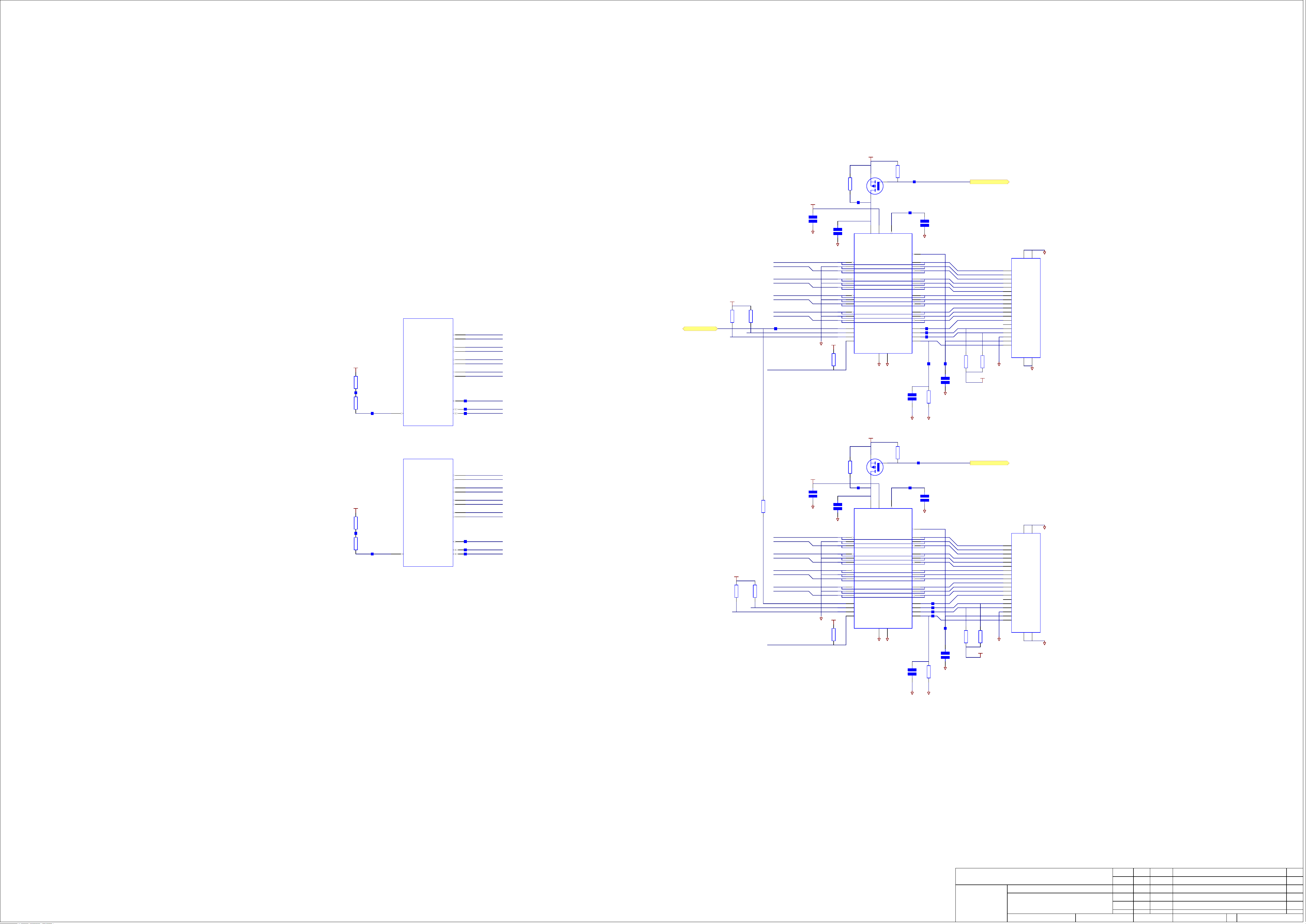
See Sheet 13
AVCC18_1
R599
680R
0W063
P1022
R598
18R
0W063
P1025
IC502C
27
SII9134
EXT_SWING
SiI9134 HDMI Tx
TX0+
TX0-
TX1+
TX1-
TX2+
TX2-
TXC+
TXC-
HPD
DSDA
DSCL
+5V_STBY
R1000
37
+5V_OUT
TMDS_BYP
TMDS_GND
TMDS_D2-
TMDS_GND
TMDS_D1-
TMDS_GND
TMDS_D0-
TMDS_GND
TMDS_CK-
CEC_OUT
GND
36
CM2020-00TR
10K
0W063
P1003
P1058
Con. side
NC
NC
NC
NC
IC1000
DGnd DGnd
DGnd
75 mA limited
38
35
34
33
32
31
30
29
28
27
26
25
24
23
22
21
20
C1027
1N0
50V
Display1_5v_off
Lo = 5v on
HiZ = 5v off
C1021
10N
50V
Ensure 5v not driven when display not selected
P1006
P1008
P1011
P1017 P1018
C1026
100N
16V
R1023
15K
DGnd
0W063
R1001
1K8
0W063
R1003
1K8
0W063
+5V_STBY
DGnd
1
2
3
4
5
6
7
8
9
10
11
12
13
14
15
16
17
18
19
21
20
SCN
SCN
Data2+
D2_Shield
Data2Data1+
D1_Shield
Data1Data0+
D0_Shield
Data0Clock+
Clk_Shield
ClockCEC
n/c
SCL
SDA
DDC/CEC Gnd
+5V
H/Plg Detect
SCN22SCN
23
DGnd
DGnd
SKT1000
WURTH ELEKTRONIK
685 119 134 923
Out 1
M1000
R1002
0R0
NF
0W063
+3v3 PW338
C1020
10N
50V
DGnd
Display1_D2+
Display1_D2-
Display1_D1+
Display1_D1-
Display1_D0+
+3v3 PW338
R1020
18K
0W063
34
33
37
36
40
39
31
30
51
47
46
Display1_D0+
Display1_D0-
Display1_D1+
Display1_D1-
Display1_D2+
Display1_D2-
Display1_CK+
Display1_CK-
P1023
Display1_Hotplug
P1024
Display1_SDA
P1026
Display1_SCL
Display_CEC
R1021
18K
0W063
Display1_D0-
Display1_CK+
Display1_CK-
P1005
Display1_SCL
Display1_SDA
Display1_Hotplug
+3v3 PW338
DGnd
DGnd
R1022
47K
0W063
C1023
10N
50V
10
11
12
13
14
15
16
17
18
4
5
6
7
8
9
NTF2955
P1004
1
2
Circ. side
5V_SUPPLY
TMDS_D2+
TMDS_GND
NC
TMDS_D1+
TMDS_GND
NC
TMDS_D0+
TMDS_GND
NC
TMDS_CK+
TMDS_GND
NC
CEC_IN
DDC_CLK_IN
DDC_DAT_IN
HOTPLUG_IN19HOTPLUG_OUT
+5V_STBY
3V3_SUPPLY
DDC_CLK_OUT
DDC_DAT_OUT
GND
3
DGndDGnd
C79, R13 see CM2020 datasheet.
See Sheet 13
AVCC18_2
R597
680R
0W063
P1037
R596
18R
0W063
P1040
IC503C
27
SII9134
EXT_SWING
SiI9134 HDMI Tx
TX0+
TX0-
TX1+
TX1-
TX2+
TX2-
TXC+
TXC-
HPD
DSDA
DSCL
R1025
37
+5V_OUT
TMDS_BYP
TMDS_GND
TMDS_D2-
TMDS_GND
TMDS_D1-
TMDS_GND
TMDS_D0-
TMDS_GND
TMDS_CK-
CEC_OUT
GND
36
CM2020-00TR
10K
0W063
NC
NC
NC
NC
IC1004
P1059
Con. side
P1027
DGnd
75 mA limited
38
35
34
33
32
31
30
29
28
27
26
25
24
23
22
21
20
C1036
1N0
50V
Display2_5v_off
Lo = 5v on
HiZ = 5v off
C1031
Ensure 5v not driven when display not selected
10N
50V
P1043
P1045
P1047
P1048
P1049
R1004
R1005
1K8
1K8
0W063
0W063
R1030
15K
0W063
DGnd
C1035
100N
16V
+5V_STBY
DGnd
1
2
3
4
5
6
7
8
9
10
11
12
13
14
15
16
17
18
19
21
20
SCN
SCN
Data2+
D2_Shield
Data2Data1+
D1_Shield
Data1Data0+
D0_Shield
Data0Clock+
Clk_Shield
ClockCEC
n/c
SCL
SDA
DDC/CEC Gnd
+5V
H/Plg Detect
SCN22SCN
23
DGnd
SKT1001
WURTH ELEKTRONIK
685 119 134 923
Out 2
DGnd
M1001
NTF2955
R1026
NF
0R0
R1029
47K
0W063
0W063
P1031
C1032
10N
50V
10
11
12
13
14
15
16
17
18
4
5
6
7
8
9
1
Circ. side
5V_SUPPLY
TMDS_D2+
TMDS_GND
NC
TMDS_D1+
TMDS_GND
NC
TMDS_D0+
TMDS_GND
NC
TMDS_CK+
TMDS_GND
NC
CEC_IN
DDC_CLK_IN
DDC_DAT_IN
HOTPLUG_IN19HOTPLUG_OUT
DGndDGnd
see CM2020 datasheet.
2
3V3_SUPPLY
DDC_CLK_OUT
DDC_DAT_OUT
GND
3
34
33
37
36
40
39
31
30
51
47
46
Display2_D0+
Display2_D0-
Display2_D1+
Display2_D1-
Display2_D2+
Display2_D2-
Display2_CK+
Display2_CK-
P1038
Display2_Hotplug
P1039
Display2_SDA
P1041
Display2_SCL
+3v3 PW338
R1027
18K
0W063
NF
R1028
18K
0W063
R1031
0R0
0W063
Display2_D2+
Display2_D2-
Display2_D1+
Display2_D1-
Display2_D0+
Display2_D0-
Display2_CK+
Display2_CK-
Display_1&2_CEC
Display2_SCL
Display2_SDA
Display2_Hotplug
+3v3 PW338
C1029
10N
50V
DGnd
DGnd
DGnd
+3v3 PW338
DGnd DGnd
DRAWING TITLE
HDMI Output MUX
ARCAM
A & R Cambridge Ltd.
Pembroke Avenue
Waterbeach
Cambridge CB5 9QR
Filename:
Notes:
Contact Engineer:
L122_C10_HDMI_Output_MUX_F0.SchDoc
Contact Tel: (01223) 203200Nick Clarke
07_E205 NC 20/11/07
PCB change onlyNC 26/3/07 B.107_E058
ECO No. DESCRIPTION OF CHANGE
INITIALS
Printed:
DATE
08/07/2008
10 13Sheet of
A1
DRAWING NO.
F.0None to this sheetPK 23/04/0808_E138
E.013/12/07PK No changes on this sheet08_E037
D.0CEC changed to bi-directional
C.0AC Present > /AC Present, HDMI EDID -> DAB I2C, Video doublerNC07_E177 16/10/07
ISSUE
L122CT
Page 61

+5V_STBY
Z3 /Mute
Z2 /Mute
/Sbl/Sbr Mute
/Main Mute
SPDIF /Reset
NET /RESET
DSP2 /CS
NET MISO_D
NET Power Down
FP RX
DAB_SDA
SPI Clk
SPI Data
AN SPI Data
RDS Int
iPod /Present
FM CE
AOut Mux Latch
Relay Sw
NET MOSI
NET SPI Clk
NET Mode Host
DSP MOSI
DSP /CS
DSP1 FLAG0
Headphone Sense
+3v3 PW338 +5V_1
CON1101
12
34
56
78
910
1112
1314
1516
1718
1920
2122
2324
2526
2728
2930
3132
3334
3536
3738
3940
4142
4344
4546
4748
4950
5152
5354
5556
5758
5960
6162
6364
6566
6768
6970
7172
7374
7576
7778
P1144
P1149
Hirose
FX8C-120S-SV5
7980
8182
8384
8586
8788
8990
9192
9394
9596
9798
99100
101102
103104
105106
107108
109110
111112
113114
115116
117118
119120
+3v3 PW338
P1143
P1169
P1171
P1174
SPDIF_Present
FAN PWM
FP TX
DAB_SCL
Zone SPI Data
AN_SCL
AN_SDA
AN SPI Clk
Zone SPI Clk
FM Data Out
RDS Data
WClk PW338
i2s mux
Vcomp Latch
VidIO Mux Latch
AIn Mux Latch
IRTrig Mux Latch
Dig Mux Latch
NET /CS
Amp_Temp_1
Amp_Temp_2
Amp_Temp_3
NET NIREQ Host
FP int
DSP MISO
DSP Clk
Y ADV7312
Pb ADV7312
Pr ADV7312
S-vid Y Out
S-vid C out
Cvid Out
1V8D
CON1100
P1101
P1105
P1109
P1113
P1116
P1120
HDMI MCLK
HDMI BCLK HDMI WCLK
Y in
S-vid Y In
NET S-vid C
Pr In
P1175
P1180
P1190
Hirose
FX8C-120S-SV5
12
34
56
78
910
1112
1314
1516
1718
1920
2122
2324
2526
2728
2930
3132
3334
3536
3738
3940
4142
4344
4546
4748
4950
5152
5354
5556
5758
5960
6162
6364
6566
6768
6970
7172
7374
7576
7778
7980
8182
8384
8586
8788
8990
9192
9394
9596
9798
99100
101102
103104
105106
107108
109110
111112
113114
115116
117118
119120
P1121
P1122
P1163
P1167
P1172
P1182
P1187
DSP2 FLAG0
Amp Fault
VSM
RS232 Tx
Z2 Demod Out
Z1 Demod Out
Z3 Demod Out
RS232 Rx
/AC Present
HDMI SPDIF
Sirius Rx
NET Rx
iPod Rx
iPod Tx
NET Tx
Sirius Tx
HDMI Data3
HDMI Data2
HDMI Data1
HDMI Data0
NET S-vid Y
Pb In
Cvid In
NET Cvid
S-vid C In
Bulk Decoupling
+5V_STBY
P1191
C1100
220UF
16V
Suface Mount
DGnd
+5V_1
C1101
220UF
16V
Suface Mount
DGnd
+3v3 PW338
C1102
220UF
16V
Suface Mount
DGnd
P1192
P1193
P1194
P1195
P1196
DRAWING TITLE
Motherboard Connections
Filename:
L122_C11_Motherboard_Connections_F0.SchDoc
DGnd DGndDGndDGnd DGndDGnd
08_E037
PK 13/12/07 E.0Re-name DSP signals for AD DSP, HDMI Clks routed to L121
1V8D
DGnd
C1103
220UF
16V
Suface Mount
P1197
P1198
F.0None to this sheetPK 23/04/0808_E138
D.020/11/07NC No changes on this sheet07_E205
ARCAM
A & R Cambridge Ltd.
Pembroke Avenue
Waterbeach
Cambridge CB5 9QR
Notes:
Contact Engineer:
C.0AC Present > /AC Present, HDMI EDID -> DAB I2C, Video doublerNC07_E177 16/10/07
PCB change onlyNC 26/3/07 B.107_E058
ECO No.
Contact Tel: (01223) 203200Nick Clarke
INITIALS
Printed:
DATE
08/07/2008
DESCRIPTION OF CHANGE
11 13Sheet of
A3
DRAWING NO.
L122CT
ISSUE
Page 62

9135 AVCC189135 AVCC33
IC201F
+5V_STBY
C1255
10uF
10V
C1256
100N
16V
11mA (0.0187W)
LM1117MPX-3.3/NOPB
REG1200
+3V3
TMDS_VA
SII9135
P1200
38
42
AVCC33
AVCC33
50
AVCC3346AVCC33
56
AVCC33
C1260
10uF
10V
DGndDGndDGnd
64
60
AVCC33
68
AVCC33
AVCC33
AVCC33
54
AVCC1837AVCC18
72
AVCC18
AVCC18SiI9135 TMDS Supplies
AGND
AGND
AGND
AGND
AGND
AGND
AGND
AGND
36
DGnd
41
45
49
53
59
63
67
AGND
71
16V
DGnd
C1200
100N
16V
L1200
220R@100MHz
10V
1V8D
C1201
10uF
10V
R1202
0R0
0W063
16V
10V
DGnd
C1202
100N
16V
C1240
10uF
10V
16V
C1203
100N
16V
16V
16V
C1241
100N
16V
16V
C1204
100N
16V
16V
C1205
100N
16V
C1242
100N
16V
16V
P1201
C1243
100N
16V
P1202
50V
50V
C1244
1N0
50V
C1208
1N0
50V
50V
50V
9135 AVCC18
50V
C1245
1N0
50V
C1246
1N0
50V
9135 AVCC33
50V
C1210
1N0
50V
50V
C1211
1N0
50V
C1212
1N0
50V
TMDS PLL Supply
TMDS Analogue Supply
SII9135
IC201G
+3v3 PW338
18
6
4
32
IOVCC33
IOVCC33
IOGND
IOGND
31
17
74
88
IOVCC33
IOVCC33
IOVCC33
IOGND
IOGND
IOGND
87
73
104
113
IOVCC33
IOVCC33
IOGND
IOGND
112
103
125
137
IOVCC33
IOVCC33
IOGND
IOGND
136
124
IOVCC33SiI9135 I/O Supplies
+3v3 PW338
1V8D
R1201
0R0
0W063
10V
DGnd
10V
DGnd
C1214
10uF
10V
10V
C1227
10uF
10V
10V
C1215
10uF
10V
C1228
10uF
10V
16V
16V
C1216
100N
16V
C1229
100N
16V
16V
16V
C1217
100N
16V
C1230
100N
16V
16V
16V
C1218
100N
16V
C1272
100N
16V
16V
16V
C1219
100N
16V
C1273
100N
16V
50V
P1203
C1231
1N0
50V
50V
C1220
1N0
50V
P1204
50V
50V
50V
C1221
1N0
50V
C1233
1N0
50V
50V
50V
C1222
1N0
50V
C1234
1N0
50V
50V
50V
C1223
1N0
50V
C1235
1N0
50V
50V
50V
C1224
1N0
50V
C1236
1N0
50V
50V
50V
C1225
1N0
50V
C1237
1N0
50V
50V
50V
C1226
1N0
50V
9135 CVCC18
50V
C1238
1N0
50V
C1239
1N0
50V
50V
C1298
1N0
50V
IO Pins Supply
C1299
1N0
50V
Digital Core Supply
+3v3 PW338
L1202
220R@100MHz
16V
P1205
C1259
100N
16V
DGnd
9135 CVCC18
107
119
131
IC201H
CVCC1812CVCC1824CVCC1825CVCC1880CVCC1891CVCC18
143
CVCC18
CVCC18
CVCC18
CVCC18
SiI9135 Digital Logic Vcc
SII9135
CGND
CGND23CGND
CGND11CGND90CGND
79
DGnd
106
CGND
118
130
CGND
0
142
EPad
+3v3 PW338
50V
16V
L1201
1V8D
16V
DGnd
120R@100MHz
L1203
C1249
100N
16V
10V
C1250
10uF
10V
16V
C1251
100N
16V
P1207
50V
DGnd
C1253
1N0
50V
DVCC18
DGnd DGnd
92
97
DVCC18
REGVCC
96
XTALVCC
SiI9135 Audio PLL
DGND
C1257
1N0
50V
IC201E
SII9135
C1258
100N
16V
120R@100MHz
DRAWING TITLE
SiI9135 Power
ARCAM
A & R Cambridge Ltd.
Pembroke Avenue
Waterbeach
Cambridge CB5 9QR
Filename:
Notes:
Contact Engineer:
L122_C12_Sii9135_Power_F0.SchDoc
Contact Tel: 01223 203200Nick Clarke
ECO No.
INITIALS
Printed:
DATE
08/07/2008
93
DGnd
PCB change onlyNC 26/3/07 B.107_E058
DESCRIPTION OF CHANGE
12 13Sheet of
A3
DRAWING NO.
F.0None to this sheetPK 23/04/0808_E138
E.013/12/07PK No changes on this sheet08_E037
D.020/11/07NC No changes on this sheet07_E205
C.0AC Present > /AC Present, HDMI EDID -> DAB I2C, Video doublerNC07_E177 16/10/07
ISSUE
L122CT
Page 63

AVCC18_1
38
32
IC502D
AVCC18
AVCC18
AVCC18_2
38
32
IC503D
AVCC18
AVCC18
+3v3 PW338
1V8D
16V
C1300
100N
16V
DGnd
+3v3 PW338
16V
C1312
100N
16V
DGnd
C1320
22uF
6.3V
L1300
60R@100MHz
L1302
60R@100MHz
P1308
P1310
16V
P1300
P1302
P1304
P1306
C1321
100N
16V
16V
C1301
22uF
6.3V
C1313
22uF
6.3V
C1322
100N
16V
16V
16V
16V
C1302
100N
16V
C1314
100N
16V
C1323
100N
16V
16V
C1303
100N
16V
AVCC33_1
50V
C1315
1N0
50V
16V
C1324
100N
16V
50V
50V
Analogue Vcc
AVCC18_1
50V
C1304
1N0
50V
C1305
1N0
50V
Analogue Vcc
IO Pins Supply
C1325
1N0
50V
50V
C1326
1N0
50V
50V
C1327
1N0
50V
+3v3 PW338
50V
C1328
1N0
50V
AVCC33_1
44
+5V_STBY
45
+3v3 PW338
89
66
53
14
43
41
35
29
26
DGnd
1v8D
55
99
76
64
12
AVCC33
DDCPWR5V
IOVCC33
IOVCC33
IOVCC33
IOVCC33
AGnd
AGnd
AGnd
AGnd
AGnd
CVCC18
CVCC18
CVCC18
CVCC18
CVCC18
+3v3 PW338
1V8D
16V
C1306
100N
16V
DGnd
+3v3 PW338
16V
C1316
100N
16V
DGnd
C1329
22uF
6.3V
L1301
60R@100MHz
L1303
60R@100MHz
P1309
P1311
16V
P1301
P1303
P1305
P1307
C1330
100N
16V
16V
C1307
22uF
6.3V
C1317
22uF
6.3V
C1331
100N
16V
16V
16V
16V
16V
C1308
100N
16V
AVCC33_2
50V
C1318
100N
16V
16V
C1332
100N
16V
Analogue Vcc
AVCC18_2
C1309
100N
16V
50V
C1310
1N0
50V
50V
Analogue Vcc
C1319
1N0
50V
C1333
100N
16V
50V
C1334
1N0
50V
50V
C1311
1N0
50V
IO Pins Supply
+3v3 PW338
50V
C1335
1N0
50V
C1337
1N0
50V
AVCC33_2
44
+5V_STBY
45
+3v3 PW338
89
66
53
14
43
41
35
29
26
DGnd
1v8D
55
99
76
64
12
AVCC33
DDCPWR5V
IOVCC33
IOVCC33
IOVCC33
IOVCC33
AGnd
AGnd
AGnd
AGnd
AGnd
CVCC18
CVCC18
CVCC18
CVCC18
CVCC18
1V8D
DGnd
C1338
22uF
6.3V
DGnd
+3v3 PW338
C1358
10uF
10V
P1312
P1314
C1359
100N
16V
16V
16V
C1339
100N
16V
38mA (0.057W)
LM1117MPX-1.8
REG1300
+1V8
C1340
100N
16V
16V
C1341
100N
16V
50V
C1361
22uF
6.3V
C1342
1N0
50V
16V
50V
PVcc
C1362
100N
16V
C1343
1N0
50V
50V
C1344
1N0
50V
Core Vcc
1v8D
50V
C1345
1N0
50V
P1317 P1318
50V
C1346
1N0
50V
L1304
60R@100MHz
PVCC2_1
42
PVCC1_1
28
100
87
65
54
13
DGnd
10V
C1363
10uF
10V
PVCC2
PVCC1
Gnd
Gnd
Gnd
Gnd
Gnd
SII9134
16V
P1320
C1364
100N
16V
SiI9134 Power & Ground Pins
PVCC2_1
50V
C1365
1N0
50V
DGnd
P1313
16V
C1347
22uF
6.3V
P1315
DGnd
C1397
100N
16V
Filter PLL Supply
16V
C1396
100N
16V
16V
16V
C1348
100N
16V
L1399
60R@100MHz
C1349
100N
16V
16V
P1316
C1350
100N
16V
50V
10V
C1351
1N0
50V
C1399
10uF
10V
P1319
50V
16V
C1352
1N0
50V
C1356
100N
16V
50V
PVCC2_2
C1353
1N0
50V
50V
DGnd
PVCC2_2
1v8D1V8D
50V
C1354
1N0
50V
50V
PVCC1_2
C1355
1N0
50V
Core Vcc
C1357
1N0
50V
Filter PLL Supply
DGnd
42
28
100
87
65
54
13
PVCC2
PVCC1
Gnd
Gnd
Gnd
Gnd
Gnd
SII9134
SiI9134 Power & Ground Pins
DGnd DGndDGnd
L1305
60R@100MHz
P1322
10V
C1369
10uF
10V
16V
P1324
DGnd
PVCC1_1
50V
C1370
100N
16V
DGnd
DRAWING TITLE
C1371
1N0
50V
TMDS PLL Supply
SiI9134 Power
Filename:
L122_C13_Sii9134_Power_F0.SchDoc
L1398
60R@100MHz
P1321
10V
C1398
10uF
10V
16V
P1323
C1366
100N
16V
PVCC1_2
50V
C1367
1N0
50V
TMDS PLL Supply
DGnd
F.0None to this sheetPK 23/04/0808_E138
E.013/12/07PK Re-name DSP signals for AD DSP, HDMI Clks routed to L12108_E037
D.020/11/07NC No changes on this sheet07_E205
ARCAM
A & R Cambridge Ltd.
Pembroke Avenue
Waterbeach
Cambridge CB5 9QR
Notes:
Contact Engineer:
C.0AC Present > /AC Present, HDMI EDID -> DAB I2C, Video doublerNC07_E177 16/10/07
PCB change onlyNC 26/3/07 B.107_E058
ECO No.
Contact Tel: (01223) 203200Nick Clarke
INITIALS
Printed:
DATE
08/07/2008
DESCRIPTION OF CHANGE
13 13Sheet of
A3
DRAWING NO.
L122CT
ISSUE
Page 64

SKT100
Emuden
M1907
L
N
CON104
1
Stocko
F/RM-0118
CON107
1
Stocko
F/RM-0118
CON106
1
Stocko
F/RM-0118
CON108
1
Stocko
F/RM-0118
Live 230V (in)
Neutral 230V (in)
C100
220N
275V
FS102
T6.3A
Bussmann / BK S506-6.3-R
FHLDR100
20mm HLDR
1A
L100
2
3
1
4
1mH
C101
220N
275V
115V 230V
2A
R100
1M5
0W5
1
2
1B
SW101
18-000-0019
2B
Neutral 115V
Neutral 230V
Bussmann / BK S506-6.3-R
FS103
T6.3A
FHLDR101
20mm HLDR
Live 230V (1) Live 230V (2)
Live 115V (1)
FS100
T800mA
Live 115V (2)
FS101
T800mA
1
4
2
5
3
CON100
MOLEX
44472
6
To STBY TFMR
4
4
4
FIX105
1
FIX106
1
FIX107
1
CON102
Stocko
F/RM-0118
To PA TFMR
CON105
1
Stocko
F/RM-0118
1
+12V_RLY
D100
BAS16
1
Thermal fuse in (230V)
Thermal fuse out (230V)
RLY100C
Takamisawa
F1CA012V
TR100
MMUN2211LT1
RELAY SW
C104
3N3
250V
C102
3N3
250V
Live 115V (4)
Live 230V (4)
RLY100B
F1CA012V
Takamisawa
R101
8A
R102
8A
+12V_RLY
RLY101C
Takamisawa
F1CA012V
D101
BAS16
TR101
MMUN2211LT1
Relay SW
23
LK100
1 2
LINK
1
23
10mm
NO FIT for AVR002
+12V_RLY
RLY102C
Takamisawa
F1CA012V
PGND
D102
BAS16
NC1
C1
RLY100A
F1CA012V
Takamisawa
SW102A
Live 230V (5)
RLY102B
Takamisawa
F1CA012V
Live 230V (6)
RLY102A
Takamisawa
F1CA012V
PGND
C103
3N3
250V
RLY101A
F1CA012V
Takamisawa
C105
3N3
250V
RLY101B
F1CA012V
Takamisawa
Live 230V (3)
Live 115V (3)
3
6
2
5
1
CON101
MOLEX
44472
To PreAmp TFMR
4
NO1
Neutral2
MSS2250R
4/8ohm switch
To PA TFMR
CON103
MOLEX
44472
Neutral1
9
PGND
7
8
1
SW102B
SW102C
23
10
NO3
MSS2250R
PGND
SP100
NC2
C2
MSS2250R
DGND
5
10
3
4
9
8
2
7
1
6
Live 115V (5)
Live 115V (6)
Switchers
L123_C2_Switchers_G0.SchDoc
Relay SW
Relay SW
NF
VGND
FIX101
Dia 3.5mm
R108
0R0
0W063
1
AGND
R103
0R0
0W063
FIX104
NF NF
1
PGND
Dia 3.5mm
R104
0R0
0W063
PGND
WARNING - PARTS MARKED WITH
NO FIT for AVP800
MUST BE REPLACED WITH IDENTICAL PARTS
FIX102
1
Dia 4.5mm
FIX103
Dia 3.5mm
TOOL100 TOOL101 TOOL102 TOOL103
FID100 FID101
FIX100
1
R106
0R0
0W063
1
PGND
Dia 3.5mm
R107
0R0
0W063
NFNF
PGND
FIX108
Dia 3.5mm
FIX109
Dia 3.5mm
1
1
R109
0R0
0W063
R110
0R0
0W063
NF
PGND
NF
PGND
ITEM102
ITEM103
PCB100 1
DRAWING TITLE
1
1
ARCAM
PSU
Filename:
Notes:
Nut M3 Full Stzp (1000)HJ3A00AITEM100 1
M Screw Torx M3x10MM ST ZPHA3V10AITEM101 1
Washer M2.9 insulating nylon shoulderHL3N
Washer M2.9 insulating nylon shoulderHL3N
Blank AVR002 PSU PCBL123PB
L123_C1_PSU_G0.SchDoc
PK
PK
PK
PK
15/09/0808_E169
16/07/0808_E157
04/04/0808_E131
21/12/0708_E018
Layout changes for safety
None to this sheet
FS102 & FS103 added, R100 footprint change, NTC changed to 2.5R
None to this sheet
G.0
F.0
E.0
D.0
A & R Cambridge Ltd.
Pembroke Avenue
Waterbeach
Cambridge CB5 9QR
Contact Engineer:
07_E178
ECO No.
Contact Tel: (01223) 203270 tel NoNick Clarke
PK
INITIALS
Printed:
18/10/07
DATE
09/10/2008
Mains isolator removed, moved to front of unit
DESCRIPTION OF CHANGE
12Sheet of
A3
DRAWING NO.
L123CT
C.0
ISSUE
Page 65

1037mA (if switchers 85% eff.)
T1 AC1
C200
100N
100V
C205
100N
100V
DBR200
GBU4K
UNREG_PW338
C201
100N
100V
C206
100N
100V
+3V3 PW338
C202
6800UF
50V
85C
HS201A
REG207
L7812CV
+12V_RLY +12V_RLY
+12
C203
220N
50V
PGND PGND
6043PB
23C/W
247mA (2.23W)
C254
100N
50V
HS202A
C255
220N
50V
6043PB
23C/W
114mA (1.56W)
REG200
L7805CV
+5V_STBYUNREG_PW338
+5
C204
100N
50V
PGND
T1 AC2
1
3
2
CON200
MOLEX From Standby TFRMR
44472
4
FS200
T2A
D200
LL4148
D201
LL4148
P200 P201 0W063
R204
4K7
0W063
C208
47N
50V
PGND
2477mA (if switchers 85% eff.)
R221
6K8
0W063
PGND
/AC Present
TR200
BC846BW
Clk PSU
C245
100P
50V
UNREG_PW338
C247
220UF
50V
105C
C252
220UF
50V
105C
2
7
5
R219
1K0
0W063
REG206
LM2670T-ADJ
VIN
BOOST
EN
SYNC
OUT
NFB
4
3
1
6
R220
1K0
0W063
R222
C244
10N
50V
R217
270R
0W063
D209
MBRS360T3G
10R
P225
P202
33uH
R218
390R
0W063
10N
L200
3.0A
C253
50V
C210
220UF
25V
105C
PGND
L204
1uH
C217
220UF
25V
105C
10A
2363mA
1V8D
C256
100UF
10V
105C
HS203A
6043PB
23C/W
T2 AC1
T2 AC2
T2 AC3
FS201
T4A
CON204
1
2
JST
VH
NF - Fit for AudioControl
C213
100N
100V
C218
100N
100V
C222
100N
100V
C228
100N
100V
DBR201
GBU8D
DBR202
W02G
C214
100N
100V
C219
100N
100V
C223
100N
100V
C229
100N
100V
UNREG
C216
6800UF
35V
105C
PGND
25mA
+40V_VFD
C225
100UF
100V
105C
Clk PSU
Clk PSU
C209
100P
50V
C215
100P
50V
UNREG_PW338
C211
220UF
50V
105C
PGND
UNREG
C220
220UF
50V
105C
2
7
5
R202
1K0
0W063
2
7
5
R207
1K0
0W063
PGND
REG201
LM2670T-ADJ
VIN
BOOST
EN
SYNC
REG202
LM2670T-ADJ
VIN
EN
SYNC
OUT
NFB
4
BOOST
OUT
NFB
4
3
1
6
3
1
6
R203
1K0
0W063
R208
1K0
0W063
R223
C207
10N
50V
R200
100R
0W063
D202
MBRS360T3G
C212
10N
50V
R205
130R
0W063
D203
MBRS360T3G
10R
0W063
P205
P216
R201
1K6
0W063
R224
10R
0W063
R206
3K0
0W063
P203
3.0A
P204
33uH
10N
10N
L201
33uH
L202
3.0A
C257
50V
C226
220UF
25V
105C
C259
50V
C248
220UF
25V
105C
PGND
PGND
L205
1uH
C246
220UF
25V
105C
L206
1uH
C249
220UF
25V
105C
1918mA
+3V3 PW338
10A
2545mA
+5V_1
10A
C260
100UF
10V
105C
C258
100UF
10V
105C
HS204A
6043PB
23C/W
HS205A
6043PB
23C/W
T2 AC4
1
5
2
6
3
7
4
CON201
MOLEX
44472
8
T2 AC5
T2 AC6
T2 AC7
From Preamp TFRMR
FS203
T2A
FS204
T2A
C234
100N
100V
C237
100N
100V
DBR203
GBU4K
REG204/5 mounted here
HS200
C235
100N
100V
C238
100N
100V
FS202
T100mA
C232
1UF
50V
105C
C233
6800UF
50V
85C
C236
6800UF
50V
85C
C239
1UF
50V
105C
LM317T
REG204
ADJ
R214
2K7
0W125
R215
2K7
0W125
ADJ
REG205 LM337T
D205
S1D
R213
240R
0W063
C243
10UF
50V
105C
R216
240R
0W063
D208
C242
10UF
50V
105C
S1D
D206
S1D
D207
S1D
PGND
872mA (11W)
+15V
C231
1uF
25V
C230
1000UF
25V
105C
PGND
C241
1uF
25V
C240
1000UF
25V
105C
-15V
375mA (5.6W)
C224
Clk PSU
100P
50V
PGND
UNREG
105C
PGND
C227
220UF
50V
2
7
5
R211
1K0
0W063
REG203
LM2670T-ADJ
VIN
BOOST
EN
SYNC
OUT
NFB
4
3
1
6
R212
1K0
0W063
PH
CON202
JST
C221
10N
50V
R209
1K0
0W063
D204
MBRS360T3G
1
2
3
4
5
6
DGND
R225
10R
0W063
P224
Clk PSU
Relay SW
/AC Present
P206
R210
3K0
0W063
10N
33uH
L203
3.0A
Relay SW
C261
50V
C250
220UF
25V
105C
PGND
L207
1uH
C251
220UF
25V
105C
10A
+5V_STBY
1V8D
DGND
AGND
VGND
2509mA
+6V_1
105C
CON203
7
8
9
10
11
12
MOLEX
44472
C262
100UF
10V
HS206A
6043PB
23C/W
+3V3 PW338
1
+5V_1
2
+6V_1
3
+40V_VFD
4
+15V
5
6
-15V
ITEM201
1
530002B02500G
2.6C/W
ITEM200
1
DRAWING TITLE
PSU - Switchers
ARCAM
A & R Cambridge Ltd.
Pembroke Avenue
Waterbeach
Cambridge CB5 9QR
Filename:
Notes:
Contact Engineer:
L123_C2_Switchers_G0.SchDoc
Contact Tel: (01223) 203270 tel NoNick Clarke
08_E169
07_E178
ECO No.
PK
PK
PK
PK
INITIALS
Printed:
16/07/0808_E157
04/04/0808_E131
18/10/07
DATE
09/10/2008
Layout changes for safety
CON204 change to increase bridge rec AC input clearences
C211, 220, 225, 227, 242, 243, 247, 252, changed to 105C
Heatsinks added to switching regs.PK 21/12/0708_E018
R217 > 270R, heatsinks added to switchers
DESCRIPTION OF CHANGE
22Sheet of
A3
DRAWING NO.
G.0
F.0
E.0
D.0
C.0
ISSUE
L123CT
Page 66

NF
R111
4R7
2W
C107 100N
NF
100V
OUT_L
OUT_C
R101
4R7
L101
1U0
2W
10A
R100
4R7
L100
1U0
G5PA-2 24VDC
RLY103A
Omron
RLY103B
2W
10A
NF
R112
1W
4R7
RLY100A
Omron
G5PA-2 24VDC
LK102
15mm
LK103
15mm
C100
10N
LS_L+
LS_C+
NF
100V
G P PRECISION
LS100
GND_L
LK100
15mm
LK101
15mm
GND_C
RLY_SB
LK105
15mm
R108
22K
0W25
LK104
15mm
D101
1N4003
TR103
BC547B
LK113
15mm
RLY101C
Omron
G5PA-2 24VDC
OUT_R
OUT_SL
R102
4R7
L102
1U0
R105
4R7
L103
Omron
G5PA-2 24VDC
NF
R113
1W
4R7
NF
R114
2W
4R7
R124
4R7
R115
4R7
2W
RLY100B
10A
Omron
G5PA-2 24VDC
2W
RLY102A
C108 100N
NF
NF
2W
C113 100N
NF
1W
10N
100V
C102
10N
LS_R+
LS_SL+
C101
NF
100V
NF
100V
100V
NF
LS101
GND_R
GND_SL
RLY_POWER
RLY_REST
R106
22K
0W25
LK109
15mm
D102
1N4003
TR102
BC547B
RLY102C
Omron
G5PA-2 24VDC
R103
22K
0W25
LK106
15mm
STARGND_DEC
D103
1N4003
TR100
BC547B
LK111
15mm
RLY103C
Omron
G5PA-2 24VDC
LK112
15mm
RLY_RESTRLY_REST
LK107
15mm
LK114
15mm
R104
22K
0W25
LK108
15mm
D100
1N4003
TR101
BC547B
RLY100C
Omron
G5PA-2 24VDC
OUT_SR
10A
1U0
R107
4R7
L104
10A
1U0
OUT_SBL
2W
NF
R118
4R7
NF
R119
4R7
R109
4R7
L105
Omron
G5PA-2 24VDC
R116
4R7
1W
NF
R117
2W
4R7
NF
1W
C110 100N
2W
NF
R120
4R7
2W
C103
10N
C109 100N
RLY102B
Omron
C104
NF
10N
100V
100V
NF
2W
NF
R121
1W
4R7
RLY101A
G P PRECISION
NF
100V
100V
NF
LS_SR+
G5PA-2 24VDC
GND_SR
NF
C111 100N
100V
C105
10N
NF
100V
LS_SBL+
LS102
LS103
GND_SBL
STARGND_DEC
CON100
SAMTEC
SSQ
From top amp
LK110
15mm
1
2
3
4
5
6
7
8
9
10
11
12
13
14
15
16
17
18
19
20
GND_SBL
GND_SBR
GND_L
GND_R
GND_SR
OUT_SR
GND_SL
OUT_SL
GND_C
OUT_C
CON101
SAMTEC
SSQ
From bottom amp
20
19
18
17
16
15
14
13
12
11
10
9
8
7
6
5
4
3
2
1
STARGND_DEC
RLY_SB
RLY_REST
RLY_POWER
GND_SBL
OUT_SBL
GND_SBR
OUT_SBR
GND_L
OUT_L
GND_R
OUT_R
FIX102
Dia 3.2mm
FIX100
Dia 3.5mm
FIX103
1
Dia 3.2mm
FIX101
1
Dia 3.5mm
FIX104
1
Dia 3.2mm
1
1
TOOL100 TOOL101 TOOL102 TOOL103
FD100 FD101
OUT_SBR
1U0
R110
4R7
L106
1U0
10A
10A
2W
NF
R123
4R7
Omron
G5PA-2 24VDC
RLY101B
Omron
G5PA-2 24VDC
NF
R122
4R7
2W
C106
1W
C112 100N
LS_SBR+
NF
10N
100V
NF
G P PRECISION
100V
GND_SBR
DRAWING TITLE
AVR002 SPEAKER PCB
ARCAM
A & R Cambridge Ltd.
Pembroke Avenue
Waterbeach
Cambridge CB5 9QR
Filename:
Notes:
Contact Engineer:
Blank AVR002 Speaker PCBL124PBPCB100 1
L124_C1 BoardSpeaker_D0.SchDoc
Contact Tel: (01223) 203265 tel NoJohn Dawson
ECO No.
PK relays now connected to stargnd_dec (drawing change only) D.015/07/0808_E144
PK
PK PCB change only, move amp connectors to correct spacing B.014/03/0707_E196
PK INITIAL RELEASE A.0.1
INITIALS
Printed:
15/2/07
DATE
17/07/2008
NF all zobel networks, change PCB for side fixing.
Output resistor changed to allow auto insert at GPE
DESCRIPTION OF CHANGE
11Sheet of
A3
DRAWING NO.
C.023/04/0808_E132
ISSUE
L124CT
Page 67

FD100 FD101 FD102 FD103
MOLEX
CON106
3
2
44472
U_Driver_C
L125_C7_DRIVER_C_D.0.SchDoc
+IN_C
ERR_NEG
ERR_POS
+IN_SR
+IN_SL
U_PSU
L125_C2_PSU_D.0.SchDoc
AC_LO_1
AC_LO_2
6
5
AC_LO_1
AC_LO_2
AC_HI_1
AC_HI_2
N LIFT OFF
P LIFT OFF
+IN_SR
+IN_SL
+IN_C
SRCE_C
SINK_C
VEE_BSTRAP_C
ERR_NEG
ERR_POS
U_Driver_SL
L125_C8_DRIVER_SL_SR_D.0.SchDoc
ERR_NEG
ERR_POS
SRCE_SR
SINK_SR
VEE_BSTRAP_S
OUT_SR
SRCE_SL
SINK_SL
+_IN_SR
+_IN_SL
OUT_SL
N LIFT OFF
P LIFT OFF
STARGND_DEC
OUT_C
SRCE_C
SINK_C
SRCE_SR
SINK_SR
SRCE_SL
SINK_SL
U_PA_C
L125_C4_PA_C_D.0.SchDoc
SRCE_C
SINK_C
VEE_BSTRAP_C
U_PA_SR
L125_C5_PA_SR_D.0.SchDoc
SRCE_SR
SINK_SR
VEE_BSTRAP_S
U_PA_SL
L125_C3_PA_SL_D.0.SchDoc
SRCE_SL
SINK_SL
VEE_BSTRAP_S
SP100
OUT_C
GND_C
TEMP_3
PLD_C
NLD_C
PLD_C
NLD_C
OUT_SR
GND_SR
PLD_C
NLD_C
OUT_SL
GND_SL
TEMP_3
NLD_C
HS100
HS GPE TO-220 GPE 5400-1702+0 14CW - RoHS
+VLO
U_Lifter_C
L125_C6_LIFTER_C_SR_D.0.SchDoc
PLD_C
NLD_C
N LIFT OFF
P LIFT OFF
-VLO
D101
PLD_C
HS GPE TO-220 GPE 5400-1702+0 14CW - RoHS
MBR1060G
HS101
+VLIFT_C+_IN_C
D100
MBR1060G
+VLIFT_C-VLIFT_C
-VLIFT_C
TOOL100 TOOL101 TOOL102 TOOL103
OUT_C
GND_C
OUT_SL
GND_SL
OUT_SR
GND_SR
CON100
1
2
3
4
5
6
7
8
9
10
11
12
13
14
15
16
17
18
19
20
HARWIN
M20-972
CON103
1
2
3
4
5
6
7
8
9
10
11
12
13
14
15
16
17
18
19
20
VEE
-VLO
+VLO
DGND
VCC
STARGND_DEC
TEMP_3
N LIFT OFF
P LIFT OFF
ERR_NEG
ERR_POS
+IN_C
+IN_SR
+IN_SL
+5V
+7V
-7V
GND_R
GND_L
GND_SBL
GND_SBR
TO/FROM BOTTOM BOARD
BOTTOM ENTRY SOCKET
100N
100N
TO SPEAKER BOARD
RIGHT ANGLED SOCKET
CON105
20
19
18
17
16
15
14
13
12
11
10
9
8
7
6
5
4
3
2
1
MOLEX
Hdr Plug Dual ROW 0.1IN RA 20WAY
C100
AC_LO_2
100V
C101
AC_LO_1
100V
1
STARGND_DEC
4
AC_HI_1
AC_HI_2
GND_R
GND_SBR
FIX100
GND_SBL
GND_C
NF
R100
0R0
0W25
STARGND_DEC
FIX101
STARGNDDGND AGND_FF
FIX102
R101
0R0
0W25
FIX103
4
FIX104
1
23
1
FIX105
FIX106
GND_SR
GND_SLGND_L
2
DRAWING TITLE
HARWIN
M20-972
M Screw Pan Supa M3x6MM ST ZPHA3A06AITEM103
Blank AVR002 AMP UPPER PCBL125PBPCB100 1
Spacer Self-Retaining M3x9.5mm NylonF293ITEM102 1
Spacer Self-Retaining M3x9.5mm NylonF293ITEM101 1
Spacer Self-Retaining M3x9.5mm NylonF293ITEM100 1
PK 13/02/08
AGND_FF
STARGND
STARGND_DEC
Added lifter mod, HS100,101 changed to GPE part, R100 NF
C100, C101 added (removed from bottom PCB)
D.008_E042
Upper Amp Main
1
1
1
1
1
1
PK 08/01/07 None to this sheet C.008_E038
Dia 3.5mm
Dia 3.5mm
Dia 3.5mm
Dia 3.5mm
Dia 3.5mm
Dia 3.5mm
ARCAM
A & R Cambridge Ltd.
Pembroke Avenue
Waterbeach
Cambridge CB5 9QR
Filename:
Notes:
Contact Engineer:
L125_C1_BoardUpper_D.0.SchDoc
Contact Tel: (01223) 203200 tel NoJohn Dawson
ECO No.
PK 24/10/07 Layout change, CON106 to 6 way, bootstrap supply added B.007_E190
PK 28/02/07 Value changes on output and lifter A.107_E041
PK 02/06/07 Initial Release A.0.1
INITIALS
Printed:
DATE
14/07/2008
DESCRIPTION OF CHANGE
18Sheet of
A3
DRAWING NO.
L125CT
ISSUE
Page 68

VCC
AC_HI_1
AC_HI_2
AC_HI_1
AC_HI_2
DBR201
GSIB2520
C208
100N
200V
C211
100N
200V
C209
100N
200V
C212
100N
200V
C206
10,000UF
80V
C210
10,000UF
80V
C207
10,000UF
80V
C213
10,000UF
80V
STARGND_DEC
VEE
R201
10K
0W063
R202
1K0
0W063
VCC+VLO
R200
100K
0W063
TR201
MMBTA06W
P LIFT OFF
TR200
MMBTA06W
AC_LO_1
AC_LO_1
DBR202
GSIB2520
C216
100N
200V
C217
100N
200V
C214
6800UF
50V
C215
6800UF
50V
+VLO
R203
1K0
0W063
R204
10K
0W063
-VLO VEE
VCC
R206
TR202
MMBTA56W
R205
100K
0W063
+VLO
STARGND_DEC
TR203
MMBTA56W
N LIFT OFF
AC_LO_2
AC_LO_2
C218
100N
200V
C219
100N
200V
C220
6800UF
50V
C221
6800UF
50V
STARGND_DEC
-VLO
VEE
3K3
0W5
R207
3K3
0W5
-VLO
DRAWING TITLE
PSU
ARCAM
A & R Cambridge Ltd.
Pembroke Avenue
Waterbeach
Cambridge CB25 9QR
Filename:
Notes:
Contact Engineer:
L125_C2_PSU_D.0.SchDoc
PK 13/02/08 Lifter cut out added, power supply bleed resistors added D.008_E042
PK 08/01/07 None to this sheet C.008_E038
PK 24/10/07 Layout change, driver PSU removed B.007_E190
PK 28/02/07 Value changes on output and lifter A.107_E041
PK 02/06/07 Initial Release A.0.1
ECO No.
Contact Tel: (01223) 203200 tel NoJohn Dawson
INITIALS
Printed:
DATE
14/07/2008
DESCRIPTION OF CHANGE
28Sheet of
A3
DRAWING NO.
L125CT
ISSUE
Page 69

SRCE_SL
SINK_SL
SRCE_SLSINK_SL
C303
10UF
100V
R301 100R
C304
100N
100V
This device must
track its relevant
driver's temperature
TR306B
NJL3281DG
TR309B
NJL1302DG
RV300
200R
LIN
TR301
BC337-40
D303
BAT54
TR308
BC847BW
R321
62R
C300
100P
50V
NF
R304
2K7
TR302
BC847BW
TR310
BC857BW
0W063
R300 100R
R302 820R
STARGND
R335
68K
0W125
VCC
TR300
MPSA42
R303
68R
0W33
R311
560R
0W25
R319
560R
0W25
C301
470P
200V
D301
BAS21LT1
VCC
R329
1R0
0W33
C309
4U7F
100V
R312
68R
0W25
R318
68R
0W25
STARGND_DEC
HS300
5400-9130+0
20C/W
TR303
MJE15034G
NJL3281DG
R333
2R2
0W25
NJL1302DG
R334
TR306A
R308
0R1
5W
TR309A
+VLIFT_C
FS300
7.0A
1206
D302
1N4003
R307 430R
R317
4R7
2W
R305
12K
0W25
R320
430R
R309
330R
R315
330R
DZ300
BZX384C
R310
2K7
R316
2K7
27V 5%
C302
10uF
10V
C305
10uF
10V
R306
12K
0W25
1K0
R313
1K0
R314
D300
BAS316
TR304
BC846BW
R336
10R
R337
3R3
0W063
0W063
TR305
BC856BW
PLD_C
OUT_SL
PLD_C
OUT_SL
R331
10K
0W063
CON300
2
1
HARWIN
M20-973
R332
10K
0W063
100R
This device must
track its relevant
driver's temperature
TR316
BC327-40
TR312
BC857BW
R323
1K0
0W063
C308
100P
50V
STARGND
R326 820R
NF
R328 100RR327
R338
68K
0W125
D306
BAS21LT1
R324
68R
0W33
TR315
MPSA92
C307
470P
200V
2R2
0W25
TR314
MJE15035G
HS301
5400-9130+0
20C/W
C310
4U7F
100V
R330
STARGND_DEC
1R0
0W33
D305
1N4003
FS301
7.0A
1206
GND_SL
C306
100N
100V
BZX384C
R325
12K
0W25
DZ301
27V 5%
R322
12K
0W25
D304
BAS316
R339
1K0
1W
C311
47UF
100V
NLD_C
NLD_C
PLACE CAPS CLOSE TO DRIVER COLLECTORS
VEE
DRAWING TITLE
-VLIFT_C
4
GND_SL
M Screw Pan Supa M3x6MM ST ZPHA3A06AITEM300
Surround Left
VEE_BSTRAP_S
PK 13/02/08
PK 08/01/07 C310 polarity corrected C.008_E038
Dual BAS21 diode replaced with singles
dual protection transistor replaced with singles. R336, 337 moved
D.008_E042
ARCAM
A & R Cambridge Ltd.
Pembroke Avenue
Waterbeach
Cambridge CB25 9QR
Filename:
Notes:
Contact Engineer:
L125_C3_PA_SL_D.0.SchDoc
Contact Tel: (01223) 203200 tel NoJohn Dawson
ECO No.
PK 24/10/07 Bootstrap network added, R335,336,337,338 B.007_E190
PK 28/02/07 Value changes on output and lifter A.107_E041
PK 02/06/07 Initial Release A.0.1
INITIALS
Printed:
DATE
14/07/2008
DESCRIPTION OF CHANGE
38Sheet of
A3
DRAWING NO.
L125CT
ISSUE
Page 70

R401 100R
This device must
track its relevant
driver's temperature
TR401
BC337-40
C400
100P
50V
R404
2K7
TR402
BC847BW
0W063
R400 100R
NF
R402 820R
STARGND
R433
68K
0W125
VCC
TR400
MPSA42
R403
68R
0W33
D401
BAS21LT1
C401
470P
200V
VCC
R429
1R0
0W33
C409
4U7F
100V
STARGND_DEC
HS400
5400-9130+0
20C/W
TR403
MJE15034G
NJL3281DG
+VLIFT_C
TR406A
FS400
7.0A
1206
R405
12K
0W25
DZ400
BZX384C
27V 5%
R406
12K
0W25
D400
BAS316
PLD_C
PLD_C
SRCE_C
SINK_C
C403
10UF
100V
C404
100N
100V
TR406B
NJL3281DG
TR409B
NJL1302DG
RV400
200R
LIN
D403
BAT54
TR408
BC847BW
R421
62R
TR410
BC857BW
R411
560R
0W25
R419
560R
0W25
R434
2R2
0W25
R412
68R
0W25
R418
68R
0W25
R435
R408
0R1
5W
TR409A
NJL1302DG
D402
1N4003
R407 430R
R417
4R7
2W
R420
430R
R409
330R
R415
330R
R410
2K7
R416
2K7
C402
10uF
10V
R413
1K0
R414
C405
10uF
10V
1K0
TR404
BC846BW
R436
10R
R437
3R3
0W063
0W063
TR405
BC856BW
OUT_C
OUT_C
R431
10K
0W063
R432
10K
0W063
CON400
2
1
HARWIN
M20-973
SINK_C SRCE_C
100R
This device must
track its relevant
driver's temperature
TR416
BC327-40
TR412
BC857BW
R423
1K0
0W063
NF
C408
100P
50V
STARGND
R426 820R
R428 100RR427
R438
68K
0W125
D406
BAS21LT1
R425
68R
0W33
TR415
MPSA92
C407
470P
200V
2R2
0W25
TR414
MJE15035G
HS401
5400-9130+0
20C/W
C410
4U7F
R430
1R0
0W33
100V
STARGND_DEC
D405
1N4003
FS401
7.0A
1206
GND_C
C406
100N
100V
BZX384C
R424
12K
0W25
DZ401
27V 5%
R422
12K
0W25
D404
BAS316
R439
1K0
1W
C411
47UF
100V
NLD_C
NLD_C
TEMP_3
TEMP_3
C413
100N
16V
R440
470R
VEE
-VLIFT_C
GND_C
VEE_BSTRAP_C
+5V
1
IC400
LM19
2
Vout
+Vs
GND
3
C412
100N
16V
DGND
DRAWING TITLE
Centre
ARCAM
A & R Cambridge Ltd.
Pembroke Avenue
Waterbeach
Cambridge CB25 9QR
Filename:
Notes:
Contact Engineer:
M Screw Pan Supa M3x6MM ST ZPHA3A06AITEM400 4
L125_C4_PA_C_D.0.SchDoc
Contact Tel: (01223) 203200 tel NoJohn Dawson
07_E190
ECO No.
PK 13/02/08
PK 08/01/07 C410 polarity corrected C.008_E038
PK 24/10/07 Bootstrap network added, R433,436,437,438 B.0
PK 28/02/07 Value changes on output and lifter A.107_E041
PK 02/06/07 Initial Release A.0.1
INITIALS
Printed:
DATE
14/07/2008
Dual BAS21 diode replaced with singles
dual protection transistor replaced with singles. R435, 437 moved
DESCRIPTION OF CHANGE
48Sheet of
A3
DRAWING NO.
D.008_E042
ISSUE
L125CT
Page 71

R501 100R
This device must
track its relevant
driver's temperature
TR501
BC337-40
C500
100P
50V
R504
2K7
TR502
BC847BW
NF
0W063
R500 100R
R502 820R
STARGND
R535
68K
0W125
VCC
TR500
MPSA42
R503
68R
0W33
D501
BAS21LT1
C501
470P
200V
VCC
R529
1R0
0W33
C509
4U7F
100V
STARGND_DEC
HS500
5400-9130+0
20C/W
TR503
MJE15034G
NJL3281DG
+VLIFT_C
TR506A
FS500
7.0A
1206
R505
12K
0W25
DZ500
BZX384C
27V 5%
R506
12K
0W25
D500
BAS316
PLD_C
PLD_C
SRCE_SR
SINK_SR
SRCE_SRSINK_SR
C503
10UF
100V
C504
100N
100V
TR506B
NJL3281DG
TR509B
NJL1302DG
RV500
200R
LIN
D503
BAT54
TR508
BC847BW
R521
62R
TR510
BC857BW
R511
560R
0W25
R519
560R
0W25
R533
2R2
0W25
R512
68R
0W25
R518
68R
0W25
R534
R508
0R1
5W
TR509A
NJL1302DG
D502
1N4003
R507 430R
R517
4R7
2W
R520
430R
R509
330R
R515
330R
R510
2K7
R516
2K7
C502
10uF
10V
R513
1K0
R514
C505
10uF
10V
1K0
TR504
BC846BW
R536
10R
R537
3R3
0W063
TR505
BC856BW
0W063
OUT_SR
OUT_SR
R531
10K
0W063
CON500
2
1
HARWIN
M20-973
R532
10K
0W063
100R
This device must
track its relevant
driver's temperature
TR516
BC327-40
TR512
BC857BW
R523 1K0
0W063
C508
100P
50V
STARGND
R526 820R
R528 100RR527
R538
68K
0W125
D506
BAS21LT1
R525
68R
0W33
TR515
MPSA92
C507
470PNF
200V
2R2
0W25
TR514
MJE15035G
HS501
5400-9130+0
20C/W
C510
4U7F
R530
1R0
0W33
100V
STARGND_DEC
D505
1N4003
FS501
7.0A
1206
GND_SR
C506
100N
100V
BZX384C
R524
12K
0W25
DZ501
27V 5%
R522
12K
0W25
D504
BAS316
C511
47UF
100V
R539
1K0
1W
NLD_C
NLD_C
VEE
-VLIFT_C
DRAWING TITLE
GND_SR
M Screw Pan Supa M3x6MM ST ZPHA3A06AITEM500 4
Surround Right
VEE_BSTRAP_S
PK 13/02/08
PK 08/01/07 C510 polarity corrected C.008_E038
Dual BAS21 diode replaced with singles
dual protection transistor replaced with singles. R536, 537 moved
D.008_E042
ARCAM
A & R Cambridge Ltd.
Pembroke Avenue
Waterbeach
Cambridge CB25 9QR
Filename:
Notes:
Contact Engineer:
L125_C5_PA_SR_D.0.SchDoc
Contact Tel: (01223) 203200 tel NoJohn Dawson
07_E190
ECO No.
PK 24/10/07 Bootstrap network added, R535,536,537,538 B.0
PK 28/02/07 Value changes on output and lifter A.107_E041
PK 02/06/07 Initial Release A.0.1
INITIALS
Printed:
DATE
14/07/2008
DESCRIPTION OF CHANGE
58Sheet of
A3
DRAWING NO.
L125CT
ISSUE
Page 72

D600
R614
PLD_C
P LIFT OFF
D602
LL4148
PLD_C
C601
47P
50V
R602
22K
C602
22P
100V
R603
22K
0W063
R600
10K
0W063
TR602
BC846BW
LL4148
TR600
BC846BW
TR601
MMBTA56W
R616
1K0
0W063
47K
0W063
R601
10R
C600
100P
50V
NF
VCC
R604
510R
M601
FQA47P06
DZ600
BZX384B
5V1 2%
+VLIFT_C
C605
47UF
100V
+VLIFT_C
NLD_C
N LIFT OFF
NLD_C
D603
LL4148
STARGND
C603
47P
50V
R605
100K
R607
100K
R611
22K
0W063
R610
22K
C607
22P
100V
TR603
BC856BW
R617
1K0
0W063
C604
TR604
MMBTA06W
R612 10R
100P
50V
NF
R606
22K
0W25
R608
22K
0W25
R609
510R
DZ601
BZX384B
5V1 2%
M603
FQA85N06
STARGND_DEC
C606
47UF
100V
-VLIFT_C
WIRE DIRECTLY TO
MOSFET SOURCE PINS
-VLIFT_C
R613
10K
0W063
DRAWING TITLE
TR605
BC856BW
D601
LL4148
R615
47K
0W063
VEE
PK 13/02/08 R616 & R617 added D.008_E042
Lifter - Centre
ARCAM
A & R Cambridge Ltd.
Pembroke Avenue
Waterbeach
Cambridge CB25 9QR
Filename:
Notes:
Contact Engineer:
L125_C6_LIFTER_C_SR_D.0.SchDoc
Contact Tel: (01223) 203200 tel NoJohn Dawson
ECO No.
PK 08/01/07 Change M603 to 85N06 type C.008_E038
PK 24/10/07 Layout change, D600,601,R614,R615 added B.007_E190
PK 28/02/07 Value changes on output and lifter A.107_E041
PK 02/06/07 Initial Release A.0.1
INITIALS
Printed:
DATE
14/07/2008
DESCRIPTION OF CHANGE
68Sheet of
A3
DRAWING NO.
L125CT
ISSUE
Page 73

AGND_FF
NJM2114M
IC700A
3
2
+7V
84
-7V
C700100N
1
C702100N
50V
STARGND
50V
R700
36K
0W25
R701
976R
0W063
IC701
5B4702
5
6
VCC
_
+
13
1
+Vcc
14
+Vcc
Comp
C712
100N
100V
C701
100N
100V
4
Source
Sink
STARGND_DEC
LM4702C
C703
33P
1000V
HS700
2
3
HS GPE TO-220 AAVID 14CW - RoHS
14C/W
+_IN_C
+_IN_C
STARGND
NF
AGND_FF
ERR_NEG
R705
1K0
R716
0R0
0W063
R718
0R0
0W063
R707
1K0
R709
1K0
5
6
IC700B
NJM2114M
R710
1K0
C704
1N0
100V
STARGND
7
VEE_BSTRAP_C
ERR_NEG
R702
+7V
3K0
0W063
R703 36K
R704
976R
0W063
R706 1K0
BAV99
D700
1
8
9
C708
100N
200V
VCC
R715
22R
0W25
R719
47R
0W25
+
_
2
Mute
Comp
15
TR700
BC847BW
D701
LL4148
Source
Sink
10
C709
100N
100V
C714
100N
100V
R711
22K
0W063
GND
7
12
11
STARGND_DEC
C711470N
7
STARGND
SRCE_C
SINK_C
100V
IC702B
TL072CD
C715
2u2F
50V
6
5
STARGND_DEC
C713
220P
100V
C705
33P
1000V
C707
68P
1000V
R708
3K3
0W063
R712
3M3
STARGND
OUT_C
R714
10K
0W25
SRCE_C
SINK_C
STARGND
STARGND
OUT_C
IC702A
TL072CD
1
+7V
84
-7V
C706100N
50V
3
2
C710100N
STARGND
50V
ERR_POS
ERR_POS
R717
1K0
0W063
VEE
ITEM701 1
DRAWING TITLE
R713
36K
0W25
C716
2P2
100V
Nut M3 Full Stzp (1000)HJ3A00A
M Screw Torx M3x10MM ST ZPHA3V10AITEM700 1
Driver - Centre
PK 13/02/08
PK 08/01/07 None to this sheet C.008_E038
R711 changed to 22k. R713 changed to through lead, C715,716 added
Ground links changed to resistor network, bootstrap circuit added
D.008_E042
ARCAM
A & R Cambridge Ltd.
Pembroke Avenue
Waterbeach
Cambridge CB25 9QR
Filename:
Notes:
Contact Engineer:
L125_C7_DRIVER_C_D.0.SchDoc
Contact Tel: (01223) 203200 tel NoJohn Dawson
ECO No.
PK 24/10/07 Layout change, extra Dcaps, added bootstrap clamp, 2 pole compensation B.007_E190
PK 28/02/07 Value changes on output and lifter A.107_E041
PK 02/06/07 Initial Release A.0.1
INITIALS
Printed:
DATE
14/07/2008
DESCRIPTION OF CHANGE
78Sheet of
A3
DRAWING NO.
L125CT
ISSUE
Page 74

+_IN_SL
ERR_NEG
ERR_POS
+_IN_SL
STARGND
NF
AGND_FF
R803
1K0
R827
0R0
0W063
R829
0R0
0W063
ERR_NEG
ERR_POS
R805
1K0
R8081K0
BAV99
NJM2114M
IC801A
3
2
R809 1K0
HS800
D800
+7V
84
-7V
C802100N
50V
1
100N
50VC805
STARGND
R823
1K0
0W063
AGND_FF
R804
1K0
R806
976R
0W063
C8061N0
100V
R81036K
+7V
C8071N0
100V
R802
22K
0W063
R811
3K0
0W063
IC803
5B4702
5
6
1
VCC
_
+
13
1
C820
2P2
100V
R800
36K
0W25
14
+Vcc
Mute
+Vcc
Comp
C800
470N
100V
C815
100N
100V
C801
100N
100V
4
Source
Sink
-7V
1
+7V
STARGND_DEC
LM4702C
GND
100V
8 4
100V
100N
2
3
7
STARGND
C813100N
2
3
C814
OUT_SL
IC800A
TL072CD
R801
3M3
STARGND
C803
33P
1000V
C818
220P
100V
R828
10K
0W25
C804
68P
1000V
OUT_SL
STARGND
R807 3K3
0W063
STARGND
SRCE_SL
SINK_SL
SRCE_SR
+_IN_SR
+_IN_SR
STARGND
R830
NF
AGND_FF
0R0
0W063
R831
0R0
0W063
R814
1K0
HS GPE TO-220 AAVID 14CW - RoHS
14C/W
NJM2114M
IC801B
5
R816
1K0
R8181K0 R819 1K0
6
STARGND
7
R815
1K0
ERR_NEG
D801
BAV99
R81236K
R813
976R
0W063
8
9
C810
100N
200V
VCC
+
_
2
15
Source
Comp
R821
22K
R825
1K0
0W063
Sink
10
C811
100N
100V
C817
100N
100V
0W063
12
11
STARGND_DEC
C812470N
100V
7
IC800B
TL072CD
6
5
R820
3M3
STARGND
R822
C816
220P
100V
C808
33P
1000V
C809
68P
1000V
R817
3K3
0W063
OUT_SR
SINK_SR
R824
STARGND
10K
0W25
STARGND
OUT_SR
VEE_BSTRAP_S
ERR_POS
ITEM801 1
R832
22R
0W25
R826
47R
0W25
TR800
BC847BW
D802
LL4148
VEE
36K
0W25
C821
2P2
100V
STARGND_DEC STARGND
Nut M3 Full Stzp (1000)HJ3A00A
C819
100N
16V
DRAWING TITLE
Driver Surr. L
ARCAM
A & R Cambridge Ltd.
Pembroke Avenue
Waterbeach
Cambridge CB25 9QR
Filename:
Notes:
Contact Engineer:
M Screw Torx M3x10MM ST ZPHA3V10AITEM800 1
L125_C8_DRIVER_SL_SR_D.0.SchDoc
Contact Tel: (01223) 203200 tel NoJohn Dawson
ECO No.
PK 13/02/08 D.008_E042
PK 08/01/07 None to this sheet C.008_E038
PK 24/10/07 Layout change, extra Dcaps, added bootstrap clamp, 2 pole compensation B.007_E190
PK 28/02/07 Value changes on output and lifter A.107_E041
PK 02/06/07 Initial Release A.0.1
INITIALS
Printed:
DATE
14/07/2008
R802, 821 changed to 22k. R800, 822 changed to through lead, C820,821 added
Ground links changed to resistor network, bootstrap circuit added
DESCRIPTION OF CHANGE
88Sheet of
A3
DRAWING NO.
L125CT
ISSUE
Page 75

+3V3 PW338
+6V_1
R108
20K
0W063
R110
10K
0W063
DGND
FClock1
FClock2
P120
P122
P101
R107
100R
0W125
R109
100R
0W125
P115
P116
+6V_1
DGND
+6V_1
3
2
DGND
IC100B
5
6
AD8532AR
84
C103
100N
16V
IC100A
AD8532AR
1
7
82
F2
81
F2
F2
MN32032A
ITRON
80
DISP100
ITEM100
1
Foam D/S ADH BK 3MM Thk 10MM Wide RA106 10M Reel
ITEM101
1
CHANGE BoM TO BE 2x30mm LENGTH
SIN1_CTRL
SIN
SIN2_CTRL
P129
P130
P131
IC102B
4
6
5
74HC08D
IC102A
1
3
2
17
SIN2
SIN2
16
SIN1
SIN1
15
CLK
CLK
SOUT2
14
SOUT1
13
GCP
11
12
GCP
LAT
BLK
LAT
9
10
BLK
DGND
VDD2
VSS
VSS
VDD1
6
7
8
DGND
R122
22R
0W125
+40V_VFD
C100
10UF
100V
DGND
+3V3 PW338
C102
100N
16V
3
F1
2
F1
1
F1
KBD0
KBD1
KBD2
P104
P105
P106
DGND
DGND
DGND
SDTM-610-NTR
SW100
MENU
1
C104
100P
C105
100P
C120
100P
SDTM-610-NTR
SW102
1
SDTM-610-NTR
SW106
1
2
INFO/v
2
ZONE
2
SDTM-610-NTR
SW105
10K
R113
1
SDTM-610-NTR
SW103
1
SDTM-610-NTR
SW109
1
P107 P108
SCAN0
2
MODE/^
2
MUTE VOL+VOL-
2
R112
SCAN1
10K
SDTM-610-NTR
SW104
INPUT ^INPUT v
1
SDTM-610-NTR
SW107
1
SDTM-610-NTR
SW111
1
2
DIRECT DISPLAY
2
2
SDTM-610-NTR
SW101
10K
R111
OK
1
SDTM-610-NTR
SW108
1
SDTM-610-NTR
SW110
1
P109 P125
SCAN2
2
2
2
R127
SCAN3
10K
+3V3 PW338
VDDOUT
+3V3 PW338
JTAG HEADER
CON101
MOLEX
NF
DGND
DGND
1
2
3
4
5
6
7
8
9
10
11
12
13
14
15
16
17
18
19
20
DGND
C121
10uF
10V
+3V3 PW338
+3V3 PW338
C122
100N
16V
VDDOUT
R117
47K
NF
DGND
DGND
C125
100N
16V
C113
1N0
50V
DGND
FIX103
Dia 3.5mm
C110
100N
16V
C118
100N
16V
C107
100N
16V
C119
100N
16V
VDDOUT
C123
100N
16V
DGND
C111
1uF
25V
1
R123
0R0
0W063
DGND
C124
100N
16V
C106
100N
16V
P128
C114
1uF
25V
TDI
TDO
TCK
TMS
+3V3 PW338
R121
47K
0W063
FIX104
Dia 3.5mm
1
R124
0R0
0W063
DGND
43
13
33
18
41
48
38
25
37
40
39
42
29
30
+3V3 PW338
NF
NF
NF
NF
FIX105
Dia 3.5mm
DGND
IC101B
7
VDDIN
VDDFLASH
VDDIO
VDDIO
VDDCORE
VDDCORE
VDDPLL
8
VDDOUT
JTAGSEL
TDI
TDO
TCK
TMS
ERASE
NRST
TST
AT91SAM7S32
R116
R120
R118
R119
47K
47K
47K
47K
SW113
SDTM-610-NTR
1
2
DGND
1
R125
0R0
0W063
NF
1
2
+3V3 PW338
NF
GND
GND
GND
XIN/PGMCK
XOUT
PLLRC
ADVREF
CON102
HARWIN
M20-973
CON105
HARWIN
M20-973
2
34
44
DGND
46
45
47
P126
+3V3 PW338
1
C126
100N
16V
DGND
IC102E
GND
74HC08D
+3V3 PW338
VCC
14
7
DGND
74HC08D
+3V3 PW338
NF
1
2
3
R115
1K5
50V
DGND
K_STBY
C127
100N
16V
DGND
C115
1N0
NF
R128
10K
10K
R129
P127
C116
10N
50V
+3V3 PW338
R114
10K
0W063
P110
DGND
9
10
12
13
DGND
ENC_A
ENC_B
13
C109
100P
50V
NF
IC102C
74HC08D
IC102D
74HC08D
+5V_STBY
16V
DGND DGND DGND
X100
4.00MHz
2
DGND
SDTM-610-NTR
SW112
POWER
NF
1
2
DGND
DGND
8
11
C101
100N
NF
NF
NF
NF
C108
10uF
10V
C128 10N
50V
C129 10N
50V
C130 10N
50V
C131 10N
50V
DGND
+3V3 PW338
C133
10N
50V
DRAWING TITLE
NF
CON100
MOLEX
ARCAM
A & R Cambridge Ltd.
Pembroke Avenue
Waterbeach
Cambridge CB5 9QR
+5V_STBY
+5V
O/P
GND
ITEM102
1
Pad Adhesive Spacing - Diva Remote Sensor
IR In
FP_RX
1
2
3
4
FP Int
FP_TX
5
6
7
8
Front Panel
Filename:
Notes:
Contact Engineer:
RX100
KSM-902TM1N
R102
0R0
0W063
R103
22K
NF
+5V_STBY
+6V_1
+40V_VFD
9
10
DGND
Blank AVR002 Front Panel PCBL126PBPCB100 1
L126_C1_Front Panel_F0.SchDoc
10N
50VC132
10N
50VC134
10N
50VC135
DGND
P111
NF
NF
NF
IR In
SCAN0
SCAN1
SCAN2
SCAN3
KBD0
KBD1
KBD2
LED GN
LED RED
CLK
SIN
ENC_A
ENC_B
FP_RX
FP_TX
K_STBY
GCP
FP Int
SIN2_CTRL
SIN1_CTRL
FClock2
FClock1
LAT
BLK
Contact Tel: (01223) 203270 tel NoNick Clarke
P112
IC101A
6
AD7
5
AD6
4
AD5
3
12
11
10
14
15
16
17
19
20
21
22
23
24
26
27
28
31
32
35
36
AD4
PA20/AD3
PA19/PGMD7/AD2
PA18/PGMD6/AD1
9
PA17/PGMD5/AD0
PA16/PGMD4
PA15/PGMD3
PA14/PGMD2
PA13/PGMD1
PA12/PGMD0
PA11/PGMM3
PA10/PGMM2
PA9/PGMM1
PA8/PGMM0
PA7/PGMNVALID
PA6/PGMNOE
PA5/PGMRDY
PA4/PGMNCMD
PA3
PA2/PGMEN2
PA1/PGMEN1
PA0/PGMEN0
AT91SAM7S32
FIX100
1
Dia 3.2mm
FIX102
1
Dia 3.2mm
TR100
MMUN2111LT1
R100
330R
0W063
08_E036 08/02/08
08_E019
07_E178
ECO No.
P100 P114
PK 11/03/0808_E133
PK 02/03/0707_E070
INITIALS
Printed:
+3V3 PW338
16/10/07PK
DATE
03/07/2008
FIX101
Dia 3.2mm
FIX106
Dia 3.2mm
DGND
TOOL100 TOOL101 TOOL102 TOOL103
SW102 function label changed, LEDs now run off 3v3
PCB mechanics change for GPE manufacture
DESCRIPTION OF CHANGE
1
1
3
2
1
CON107
Stocko
F/RM-0118
CON109
Stocko
F/RM-0118
TR101
MMUN2111LT1
CON104
AMP
CT
11Sheet of
Live_in
1
Neutral_in
1
CON103
AMP
CT
MAINS SWITCH SNAP OFF
R101
330R
0W063
1
2
3
FIX107
Dia 3.2mm
SW114A
SS-160-3-A
SW114B
SS-160-3-A
LED REDLED GN
P113
If = 7mA, Vf = 2V
R104
LED100
REDGRN
3mm
BICOL
150R NF
0W063
R105
150R
0W063
R106
75R
0W063
R126
75R
0W063
If = 15mA, Vf = 2V
LED SNAP OFF
FIX108
1
Dia 3.2mm
FID100 FID101
A3
DRAWING NO.
Live_out
Neutral_out
NF
1
L126CT
CON106
1
Stocko
F/RM-0118
CON108
1
Stocko
F/RM-0118
F.0
E.0NC Con100 connections changed
D.0PK 16/01/08 Power LED changed to FMJ type
C.0Rx & Tx Corrected, +5V_2 changed to +6V_1, encoder connections added
B.0KBD Rx4 moved to SCAN0..3, JTAGSEL made NC (was pulled up)
ISSUE
Page 76

+5V_1
Pullup on main PCB for 3V3 operation
Headphone Sense
Headphone L
Headphone R
DGND
SKT101
1
5
4
3
2
R
L
Headphone Out
CON100
MOLEX
52045
1
2
3
4
5
6
7
8
9
10
11
12
13
14
15
16
AGND
DGND
DGND
NF NF NF NF NF NF
C106
10N
50V
C107
10N
50V
C109
10N
50V
C110
10N
50V
C111
10N
50V
AUX SPDIF
Headphone Sense
Aux L
Aux R
Headphone L
Headphone R
C112
10N
50V
AUX SPDIF
R101
2K2
0W063
5V to 3V pad
R100
1K0
0W063
DGND
OJ002A-Rxx
O/P
DGND
+5V_1
DGND
+5V
GND
C100
100N
16V
0603
X7R
SKT100B
C108
10uF
10V
AUX L
AUX R
AGND+5V_1
AGND
WTJ-035-16CB
4
3 L
2
1
5
R
SKT100A
Mic / Aux / Aux Opt In
FIX100
4
1
NF NF
R105
0R0
0W063
DGND DGND
TOOL100 TOOL101 TOOL102 TOOL103
FID100 FID101
1
23
FIX101
4
1
R106
0R0
0W063
1
23
Blank AVR002 Front Input PCBL127PBPCB100 1
DRAWING TITLE
Front Input
ARCAM
A & R Cambridge Ltd.
Pembroke Avenue
Waterbeach
Cambridge CB5 9QR
Filename:
Notes:
Contact Engineer:
L127_C1_Front Input_E0.SchDoc
Contact Tel: (01223) 203270 tel NoNick Clarke
07_E180
07_E071
ECO No.
INITIALS
Printed:
DATE
03/07/2008
M100 changed to lower Rds on part C.1PK 11/11/0708_E020
C101 moved to main PCB. Board mechanics changed C.0PK 19/10/07
Updated PCB clearance rules BPK 02/03/07
DESCRIPTION OF CHANGE
11Sheet of
A3
DRAWING NO.
E.0PCB change only08_E134 PK 15/05/08
D.0PK 20/02/0808_E056 USB removed CON100, changed to 16 way
ISSUE
L127CT
Page 77

FIX105
CON104
MOLEX
52808
CON107
JST
XH
CON108
JST
XH
+12V
-12V
8
7
6
5
4
3
2
1
DGND
1
2
1
2
R103
1K0
0W063
R102
33R
0W25
R105
1K5
0W063
R108
1K5
0W063
R109
33R
0W25
FAN_PWM
OFFSET
TEMP_1
TEMP_2
TEMP_3
FANS_POS
C101
100UF
25V
C100
100UF
25V
STARGND_LIFT
CON110
1
2
HARWIN
M20-973
TR100
BC337-40
R106
2K7
0W063
R107
2K7
0W063
TR101
BC327-40
U_MiscLower
L129_C10_MiscLower_Iss_D.0.SchDoc
ERR_NEG
FAN_PWM
OFFSET
RLY_REST
FANS_POS
AC_LO_2
AC_LO_1
AC_LO_1
AC_LO_2
+5V
DZ100
BZX384B
5V1 2%
DGND +7V
C103
2u2F
50V
AGND_FF
C104
2u2F
50V
-7V
ERR_POS
RLY_SB
~MUTE_REST
~MUTE_SB
~MUTE_REST
~MUTE_SB
U_Driver_L
L129_C7_Driver_L_Iss_D.0.SchDoc
ERR_NEG
ERR_POS
ERR_NEG
ERR_POS
SRCE_L
SINK_L
RLY_SB
RLY_REST
VEE_BSTRAP_L
+_IN_L
+_IN_SBL
+_IN_L
+_IN_SBL
SRCE_SBL
SINK_SBL
U_Driver_R
L129_C3_Driver_R_Iss_D.0.SchDoc
ERR_NEG
ERR_POS
ERR_NEG
ERR_POS
SRCE_R
SINK_R
VEE_BSTRAP_R
+_IN_R
+_IN_SBR
+_IN_R
+_IN_SBR
SRCE_SBR
SINK_SBR
OUT_SBL OUT_L
OUT_SBR OUT_R
U_PA_L
L129_C9_PA_L_Iss_D.0.SchDoc
SRCE_L
SINK_L
VEE_BSTRAP_L
U_PA_SBL
L129_C2_PA_SBL_Iss_D.0.SchDoc
VEE_BSTRAP_L
SRCE_SBL
SINK_SBL
U_PA_R
L129_C8_PA_R_Iss_D.0.SchDoc
SRCE_R
SINK_R
U_PA_SBR
L129_C4_PA_SBR_Iss_D.0.SchDoc
VEE_BSTRAP_R
SRCE_SBR
SINK_SBR
OUT_L
GND_L
TEMP_1
PLD_L
NLD_L
PLD_L
NLD_L
OUT_SBL
GND_SBL
N LIFT OFF
P LIFT OFF
OUT_R
GND_R
TEMP_2
PLD_R
NLD_RVEE_BSTRAP_R
PLD_R
NLD_R
OUT_SBR
GND_SBR
TEMP_1
TEMP_2
D100
MBR1060G
+VLO
U_Lifter_L
L129_C5_LIFTER_L_Iss_D.0.SchDoc
D101
MBR1060G
-VLO
HS101
5400-9130+0
20C/W
+VLO
D102
MBR1060G
U_Lifter_R
L129_C6_LIFTER_R_Iss_D.0.SchDoc
-VLO
D103
MBR1060G
HS100
5400-9130+0
20C/W
PLD_L
NLD_L
N LIFT OFF
P LIFT OFF
HS102
5400-9130+0
20C/W
N LIFT OFF
P LIFT OFF
PLD_R
NLD_R
+VLIFT_L
+VLIFT_L-VLIFT_L
-VLIFT_L
+VLIFT_R
+VLIFT_R-VLIFT_R
HS103
5400-9130+0
20C/W
-VLIFT_R
+VLO
C107
220UF
50V
STARGND_LIFT
C108
220UF
50V
-VLO
STARGND_LIFT
+VLO
-VLO
C102
220UF
50V
C106
220UF
50V
TOOL100 TOOL101 TOOL102 TOOL103
FD100 FD101 FD102 FD103
OUT_R
GND_R
OUT_L
GND_L
OUT_SBR
GND_SBR
OUT_SBL
GND_SBL
HS106
5400-9130+0
20C/W
STARGND_DEC
+VLO
R104
2K2
0W25
C105
22UF
63V
DZ102
BZX384C
27V 5%
TR102
MJE15034G
STARGND_DEC
RLY_POWER
RLY_SB
RLY_REST
CON100
SAMTEC
SSQ
CON103
SAMTEC
SSQ
CON102
1
2
3
4
5
6
7
8
9
10
11
12
13
14
15
16
17
18
19
20
MOLEX
1
2
3
VEE
4
5
6
7
8
9
10
11
-VLO
12
13
14
15
+VLO
16
17
18
19
20
AC_LO_1
AC_LO_2
DGND
+5V
1
2
3
4
5
6
7
8
9
10
11
12
13
14
15
16
17
18
19
20
STARGND
STARGND_DEC
Dia 3.5mm
FIX102
Dia 3.5mm
FIX101
Dia 3.5mm
FIX106
Dia 3.5mm
FIX104
Dia 3.5mm
FIX103
Dia 3.5mm
FIX100
4
1
VCC
STARGND_LIFT
TO/FROM TOP BOARD
TEMP_3
N LIFT OFF
P LIFT OFF
+7V
-7V
ERR_NEG
ERR_POS
+_IN_C
+_IN_SR
+_IN_SL
AGND_FF
1
1
1
1
1
1
1
23
NF
R100
0R0
0W25
STARGNDDGND AGND_FF
R101
0R0
0W25
AGND_FF
+_IN_L
1
2
CON101
MOLEX
52806
10
DRAWING TITLE
-12V
+_IN_SL
9
10111213141516171819202122
7
+_IN_SW
8
+_IN_R
3
4
+_IN_C
5
6
+_IN_SR
+_IN_SBL
+_IN_SBR
+5V
~MUTE_REST
~MUTE_SB
+12V
ARCAM
A & R Cambridge Ltd.
Pembroke Avenue
Waterbeach
Cambridge CB5 9QR
Lower Amp Main
Filename:
Notes:
Contact Engineer:
M Screw Pan Supa M3x6MM ST ZPHA3A06AITEM100
Blank AVR002 AMP LOWER PCBL129PBPCB100 1
L129_C1_BoardLower_Iss_D.0.SchDoc
Contact Tel: (01223) 203200 tel NoJohn Dawson
07_E191
ECO No.
PK 13/02/08
PK 08/01/08 Swap mute lines on CON101 C.008_E039
PK 24/10/07 Bootstrap supply added dev regulators removed B.0
PK 28/02/07 Value changes on ouptut stage and lifters A.107_E042
PK 02/06/07 Initial Release A.0.1
INITIALS
Printed:
DATE
14/07/2008
Lifter mod added, R100 NF, remove large fan connectors
+/-7V supply added for driver front end op amps, relays to star_dec
DESCRIPTION OF CHANGE
110Sheet of
A3
DRAWING NO.
L129CT
D.008_E043
ISSUE
Page 78

R201 100R
This device must
track its relevant
driver's temperature
TR201
BC337-40
C200
100P
50V
R204
2K7
TR202
BC847BW
NF
0W063
R200 100R
R202 820R
STARGND
R235
68K
0W125
VCC
TR200
MPSA42
R203
68R
0W33
D201
BAS21LT1
C201
470P
200V
VCC +VLIFT_L
R229
1R0
0W33
C209
4U7F
100V
STARGND_LIFT
HS200
5400-9130+0
20C/W
TR203
MJE15034G
TR206A
NJL3281DG
FS200
7.0A
1206
R205
12K
0W25
DZ200
BZX384C
27V 5%
R206
12K
0W25
D200
BAS316
PLD_L
SRCE_SBL
SINK_SBL
C203
10UF
100V
C204
100N
100V
TR206B
NJL3281DG
TR209B
NJL1302DG
RV200
200R
LIN
D203
BAT54
TR208
BC847BW
R221
62R
TR210
BC857BW
R211
560R
0W25
R219
560R
0W25
R233
2R2
0W25
R212
68R
0W25
R218
68R
0W25
R234
R208
0R1
5W
TR209A
NJL1302DG
D202
1N4003
R207 430R
R217
4R7
2W
R220
430R
R209
330R
R215
330R
R210
2K7
R216
2K7
C202
10uF
10V
R213
1K0
R214
C205
10uF
10V
1K0
TR204
BC846BW
R236
10R
R237
3R3
0W063
TR205
BC856BW
0W063
OUT_SBL
R231
10K
0W063
CON200
2
1
HARWIN
M20-973
R232
10K
0W063
100R
This device must
track its relevant
driver's temperature
TR216
BC327-40
TR212
BC857BW
0W063
R223
1K0
STARGND
NF
C208
100P
50V
R238
68K
0W125
R226 820R
R228 100RR227
D206
BAS21LT1
R224
68R
0W33
TR215
MPSA92
C207
470P
200V
2R2
0W25
TR214
MJE15035G
HS201
5400-9130+0
20C/W
C210
4U7F
100V
R230
STARGND_LIFT
1R0
0W33
D205
1N4003
FS201
7.0A
1206
C206
100N
100V
R225
12K
0W25
DZ201
BZX384C
27V 5%
R222
12K
0W25
NLD_L
D204
BAS316
R239
1K0
1W
C211
47UF
100V
VEE -VLIFT_L
4
DRAWING TITLE
Surround Back Left
GND_SBL
VEE_BSTRAP_L
M Screw Pan Supa M3x6MM ST ZPHA3A06AITEM200
PK 13/02/08
PK 08/01/08 C210 polarity corrected C.008_E039
Dual BAS21 diode replaced with singles
dual protection transistor replaced with singles
D.008_E043
ARCAM
A & R Cambridge Ltd.
Pembroke Avenue
Waterbeach
Cambridge CB25 9QR
Filename:
Notes:
Contact Engineer:
L129_C2_PA_SBL_Iss_D.0.SchDoc
Contact Tel: (01223) 203200 tel NoJohn Dawson
ECO No.
PK 24/10/07 Bootstrap supply added, added R235,236,237,238 B.007_E191
PK 28/02/07 Value changes on ouptut stage and lifters A.107_E042
PK 02/06/07 Initial Release A.0.1
INITIALS
Printed:
DATE
14/07/2008
DESCRIPTION OF CHANGE
210Sheet of
A3
DRAWING NO.
L129CT
ISSUE
Page 79

C319
2P2
100V
R300
ERR_NEG
ERR_POS
+_IN_R
STARGND
NF
AGND_FF
+_IN_SBR
R303
1K0
R328
0R0
0W063
R329
0R0
0W063
R314
1K0
STARGND
R330
NF
0R0
0W063
ERR_NEG
D300
BAV99
ERR_POS
NJM2114M
IC301A
3
R305
1K0
R3081K0 R309 1K0
HS GPE TO-220 AAVID 14CW - RoHS
NJM2114M
IC301B
R316
1K0
2
HS300
14C/W
5
6
+7V
84
-7V
R319
1K0
C304100N
50V
1
100N
50VC307
STARGND
STARGND
7
ERR_NEG
AGND_FF
R304
1K0
R307
976R
0W063
R310 36K
+7V
C309 1N0
100V
R313
976R
0W063
R315
1K0
R323
1K0
0W063
C3081N0
100V
R311
3K0
0W063
R31236K
R302
22K
0W063
IC302
5B4702
5
6
1
8
9
C312
100N
200V
VCC
VCC
_
+
+
_
13
1
2
36K
0W25
14
+Vcc
Mute
15
C315
C303
+Vcc
Comp
Comp
C313
C318
C301
100N
STARGND
100N
100V
100N
100V
50V
4
LM4702C
Source
Sink
Source
Sink
10
100N
100V
100N
100V
C300470N
100V
1
C302
100N
50V
STARGND_DEC
2
3
GND
STARGND_DEC
7
STARGND
12
11
C314470N
8 4
100V
-7V
+7V
C306
33P
1000V
R301
2
3
IC300A
TL072CD
C317
220P
100V
C310
33P
1000V
R320 3M3
3M3
STARGND
C305
68P
1000V
C316
220P
100V
R325
10K
0W25
C311
68P
1000V
R324
10K
0W25
R306
3K3
0W063
STARGND
R3173K3
0W063
OUT_R
STARGND
STARGND
SRCE_R
SINK_R
SRCE_SBR
SINK_SBR
STARGND
OUT_SBR
R331
0R0
0W063
AGND_FF
R318
1K0
D301
BAV99
ERR_POS
VEE_BSTRAP_R
BSTRAP_R_TEST
R333
10K
0W063
R332
22R
0W25
R327
47R
0W25
R321
22K
R326
1K0
0W063
TR300
BC847BW
D302
LL4148
0W063
7
IC300B
TL072CD
6
5
STARGND
R322
36K
0W25
C320
2P2
100V
ITEM300 1
DRAWING TITLE
ARCAM
A & R Cambridge Ltd.
Pembroke Avenue
Waterbeach
Cambridge CB25 9QR
VEE
Driver Right
Filename:
Notes:
Contact Engineer:
Nut M3 Full Stzp (1000)HJ3A00A
M Screw Torx M3x10MM ST ZPHA3V10AITEM301 1
L129_C3_Driver_R_Iss_D.0.SchDoc
Contact Tel: (01223) 203200 tel NoJohn Dawson
ECO No.
PK 13/02/08 D.008_E043
PK 08/01/08 None to this sheet C.008_E039
PK 24/10/07 Bootstrap supply added, heatsink added B.007_E191
PK 28/02/07 Value changes on ouptut stage and lifters A.107_E042
PK 02/06/07 Initial Release A.0.1
INITIALS
Printed:
DATE
14/07/2008
R302, 321 changed to 22k. R300, 322 changed to through lead, C319,320 added
Ground links changed to resistor network, bootstrap circuit added
DESCRIPTION OF CHANGE
310Sheet of
A3
DRAWING NO.
L129CT
ISSUE
Page 80

R401 100R
This device must
track its relevant
driver's temperature
TR401
BC337-40
C400
100P
50V
R404
2K7
TR402
BC847BW
NF
0W063
R400 100R
R402 820R
STARGND
R435
68K
0W125
VCC
TR400
MPSA42
R403
68R
0W33
C401
470P
200V
D401
BAS21LT1
VCC +VLIFT_R
R429
1R0
0W33
C409
4U7F
100V
STARGND_LIFT
HS400
5400-9130+0
20C/W
TR403
MJE15034G
TR406A
NJL3281DG
FS400
7.0A
1206
R405
12K
0W25
DZ400
BZX384C
27V 5%
R406
12K
0W25
D400
BAS316
PLD_R
SRCE_SBR
SINK_SBR
C403
10UF
100V
C404
100N
100V
TR406B
NJL3281DG
TR409B
NJL1302DG
RV400
200R
LIN
D403
BAT54
TR408
BC847BW
R421
62R
TR410
BC857BW
R411
560R
0W25
R419
560R
0W25
R433
2R2
0W25
R412
68R
0W25
R418
68R
0W25
R434
R408
0R1
5W
TR409A
NJL1302DG
D402
1N4003
R407 430R
R417
4R7
2W
R420
430R
R409
330R
R415
330R
R410
2K7
R416
2K7
C402
10uF
10V
R413
1K0
R414
C405
10uF
10V
1K0
TR404
BC846BW
R436
10R
R437
3R3
0W063
TR405
BC856BW
0W063
OUT_SBR
R431
10K
0W063
CON400
2
1
HARWIN
M20-973
R432
10K
0W063
100R
This device must
track its relevant
driver's temperature
TR416
BC327-40
TR412
BC857BW
0W063
R423
1K0
STARGND
NF
C408
100P
50V
R438
68K
0W125
R426 820R
R428 100RR427
D406
BAS21LT1
R424
68R
0W33
TR415
MPSA92
C407
470P
200V
2R2
0W25
TR414
MJE15035G
HS401
5400-9130+0
20C/W
C410
4U7F
R430
1R0
0W33
100V
STARGND_LIFT
D405
1N4003
FS401
7.0A
1206
C406
100N
100V
R425
12K
0W25
DZ401
BZX384C
27V 5%
R422
12K
0W25
NLD_R
D404
BAS316
R439
1K0
1W
C411
47UF
100V
VEE -VLIFT_R
4
DRAWING TITLE
Surround Back Right
GND_SBR
VEE_BSTRAP_R
M Screw Pan Supa M3x6MM ST ZPHA3A06AITEM400
PK 13/02/08
PK 08/01/08 C410 polarity corrected C.008_E039
Dual BAS21 diode replaced with singles
dual protection transistor replaced with singles
D.008_E043
ARCAM
A & R Cambridge Ltd.
Pembroke Avenue
Waterbeach
Cambridge CB25 9QR
Filename:
Notes:
Contact Engineer:
L129_C4_PA_SBR_Iss_D.0.SchDoc
Contact Tel: (01223) 203200 tel NoJohn Dawson
ECO No.
PK 24/10/07 Bootstrap supply added, added R435,436,437,438 B.007_E191
PK 28/02/07 Value changes on ouptut stage and lifters A.107_E042
PK 02/06/07 Initial Release A.0.1
INITIALS
Printed:
DATE
14/07/2008
DESCRIPTION OF CHANGE
410Sheet of
A3
DRAWING NO.
L129CT
ISSUE
Page 81

D500
R514
D502
R502
22K
C506
22P
100V
0W063
R500
10K
LL4148
47K
0W063
TR500
BC846BW
R501
TR501
MMBTA56W
10R
VCC
M502
FQA47P06
P LIFT OFF
LL4148
PLD_L
C501
47P
50V
STARGND
0W063
R503
R505
100K
R507
100K
22K
TR502
BC846BW
R516
1K0
0W063
C500
100P
50V
NF
DZ500
BZX384B
5V1 2%
R504
510R
R506
22K
0W25
R508
22K
0W25
+VLIFT_L
C502
47UF
100V
STARGND_LIFT
C505
47UF
100V
N LIFT OFF
D503
LL4148
NLD_L
C503
47P
50V
R511
22K
0W063
R510
22K
C507
22P
100V
0W063
TR503
BC856BW
R517
1K0
0W063
C504
TR504
MMBTA06W
R512 10R
100P
50V
NF
R509
510R
DZ501
BZX384B
5V1 2%
M503
FQA85N06
WIRE DIRECTLY TO
MOSFET SOURCE PINS
-VLIFT_L
R513
10K
D501
LL4148
TR505
BC856BW
VEE
R515
47K
0W063
DRAWING TITLE
Lifter - Left
ARCAM
A & R Cambridge Ltd.
Pembroke Avenue
Waterbeach
Cambridge CB25 9QR
Filename:
Notes:
Contact Engineer:
L129_C5_LIFTER_L_Iss_D.0.SchDoc
Contact Tel: (01223) 203200 tel NoJohn Dawson
ECO No.
PK 13/02/08 lift off Lifter mod added D.008_E043
PK 08/01/08 Chnage M503 to 85N06 C.008_E039
PK 24/10/07 Added D500,501, R514,515 B.007_E191
PK 28/02/07 Value changes on ouptut stage and lifters A.107_E042
PK 02/06/07 Initial Release A.0.1
INITIALS
Printed:
DATE
14/07/2008
DESCRIPTION OF CHANGE
510Sheet of
A3
DRAWING NO.
L129CT
ISSUE
Page 82

D600
R614
D602
R602
22K
0W063
R600
10K
C606
22P
100V
LL4148
47K
0W063
TR600
BC846BW
R601
TR601
MMBTA56W
10R
VCC
M602
FQA47P06
P LIFT OFF
LL4148
PLD_R
C601
47P
50V
STARGND
0W063
R603
R605
100K
R607
100K
22K
TR602
BC846BW
R616
1K0
0W063
C600
100P
50V
NF
DZ600
BZX384B
5V1 2%
R604
510R
R606
22K
0W25
R608
22K
0W25
+VLIFT_R
C602
47UF
100V
STARGND_LIFT
N LIFT OFF
D603
LL4148
NLD_R
C603
47P
50V
R611
22K
0W063
R610
22K
C607
22P
100V
TR603
BC856BW
R617
1K0
0W063
C604
TR604
MMBTA06W
R612 10R
100P
50V
NF
R609
510R
DZ601
BZX384B
5V1 2%
M603
FQA85N06
C605
47UF
100V
WIRE DIRECTLY TO
MOSFET SOURCE PINS
-VLIFT_R
0W063
R613
10K
D601
LL4148
TR605
BC856BW
VEE
R615
47K
0W063
DRAWING TITLE
Lifter - Right
ARCAM
A & R Cambridge Ltd.
Pembroke Avenue
Waterbeach
Cambridge CB25 9QR
Filename:
Notes:
Contact Engineer:
L129_C6_LIFTER_R_Iss_D.0.SchDoc
Contact Tel: (01223) 203200 tel NoJohn Dawson
ECO No.
PK 13/02/08 D.008_E043
PK 08/01/08 Change M603 to 85N06, change M602 to FQA47P06 (was N channel!) C.008_E039
PK 24/10/07 Added D600,601, R614,615 B.007_E191
PK 28/02/07 Value changes on ouptut stage and lifters A.107_E042
PK 02/06/07 Initial Release A.0.1
INITIALS
Printed:
DATE
14/07/2008
lift off Lifter mod added
DESCRIPTION OF CHANGE
610Sheet of
A3
DRAWING NO.
ISSUE
L129CT
Page 83

C719
2P2
100V
R700
ERR_NEG
ERR_POS
+_IN_SBL
STARGND
NF
AGND_FF
+_IN_L
R703
1K0
R728
0R0
0W063
R729
0R0
0W063
HS GPE TO-220 AAVID 14CW - RoHS
R714
1K0
STARGND
R730
NF
0R0
0W063
ERR_NEG
D700
BAV99
ERR_POS
NJM2114M
IC701A
3
R706
1K0
R7081K0 R709 1K0
HS700
14C/W
NJM2114M
IC701B
R716
1K0
2
5
6
+7V
84
-7V
R719
1K0
C702100N
50V
1
100N
50VC705
STARGND
STARGND
7
ERR_NEG
R723
1K0
0W063
AGND_FF
R704
1K0
R707
976R
0W063
C7061N0
100V
R71036K
+7V
C7071N0
100V
R71236K
R713
976R
0W063
R715
1K0
R702
22K
0W063
R711
3K0
0W063
IC702
5B4702
5
6
1
8
9
C710
100N
200V
VCC
VCC
_
+
+
_
13
1
2
36K
0W25
14
+Vcc
Mute
15
+Vcc
Comp
Comp
C711
C718
C715
100N
100V
C701
100N
100V
4
Source
Sink
Source
Sink
10
100N
100V
100N
100V
C713
100N
50V
C714
STARGND_DEC
LM4702C
GND
STARGND_DEC
C700470N
100V
1
100N
50V
C704
33P
1000V
2
3
7
STARGND
12
11
C708
33P
1000V
C712470N
100V
IC700A
TL072CD
-7VSTARGND
8 4
+7V
68P
1000V
R701
2
3
C703
68P
1000V
C716
220P
100V
C717
220P
100V
C709
R720 3M3
3M3
STARGND
R724
10K
0W25
R725
10K
0W25
OUT_SBL
STARGND
R7053K3
0W063
STARGND
SRCE_SBL
SINK_SBL
SRCE_L
SINK_L
STARGND
STARGND
R717 3K3
0W063
OUT_L
R731
0R0
0W063
AGND_FF
R718
1K0
D701
BAV99
ERR_POS
VEE_BSTRAP_L
BSTRAP_L_TEST
R733
10K
0W063
R732
22R
0W25
R727
47R
0W25
R721
22K
R726
1K0
0W063
TR700
BC847BW
D702
LL4148
0W063
7
IC700B
TL072CD
6
5
STARGND
R722
36K
0W25
C720
2P2
100V
ITEM701 1
DRAWING TITLE
ARCAM
A & R Cambridge Ltd.
Pembroke Avenue
Waterbeach
Cambridge CB25 9QR
VEE
Driver - Left
Filename:
Notes:
Contact Engineer:
Nut M3 Full Stzp (1000)HJ3A00A
M Screw Torx M3x10MM ST ZPHA3V10AITEM700 1
L129_C7_DRIVER_L_Iss_D.0.SchDoc
Contact Tel: (01223) 203200 tel NoJohn Dawson
ECO No.
PK 13/02/08 D.008_E043
PK 08/01/08 None to this sheet C.008_E039
PK 24/10/07 Bootstrap supply added, heatsink added B.007_E191
PK 28/02/07 Value changes on ouptut stage and lifters A.107_E042
PK 02/06/07 Initial Release A.0.1
INITIALS
Printed:
DATE
14/07/2008
R702, 721 changed to 22k. R700, 722 changed to through lead, C719,720 added
Ground links changed to resistor network, bootstrap circuit added
DESCRIPTION OF CHANGE
710Sheet of
A3
DRAWING NO.
L129CT
ISSUE
Page 84

R801 100R
This device must
track its relevant
driver's temperature
TR801
BC337-40
C800
100P
50V
R804
2K7
TR802
BC847BW
NF
0W063
R800 100R
R802 820R
STARGND
R833
68K
0W125
VCC VCC +VLIFT_R
R829
1R0
TR800
MPSA42
C801
470P
200V
R803
68R
0W33
D801
BAS21LT1
0W33
C809
4U7F
100V
FS800
7.0A
1206
STARGND_LIFT
HS800
5400-9130+0
20C/W
TR803
MJE15034G
TR806A
NJL3281DG
R805
12K
0W25
DZ800
BZX384C
27V 5%
R806
12K
0W25
D800
BAS316
PLD_R
SRCE_R
SINK_R
C803
10UF
100V
C804
100N
100V
TR806B
NJL3281DG
TR809B
NJL1302DG
RV800
200R
LIN
D803
BAT54
TR808
BC847BW
R821
62R
TR810
BC857BW
R811
560R
0W25
R819
560R
0W25
R834
2R2
0W25
R812
68R
0W25
R818
68R
0W25
R835
R808
0R1
5W
TR809A
NJL1302DG
D802
1N4003
R807 430R
R817
4R7
2W
R820
430R
R809
330R
R815
330R
R810
2K7
R816
2K7
C802
10uF
10V
R813
1K0
R814
C805
10uF
10V
1K0
TR804
BC846BW
R836
10R
R837
3R3
0W063
0W063
TR805
BC856BW
OUT_R
R831
10K
0W063
CON800
2
1
HARWIN
M20-973
R832
10K
0W063
100R
This device must
track its relevant
driver's temperature
TR816
BC327-40
TR812
BC857BW
0W063
R823
1K0
STARGND
NF
C808
100P
50V
R838
68K
0W125
R826 820R
R828 100RR827
D806
BAS21LT1
R824
68R
0W33
TR815
MPSA92
C807
470P
200V
2R2
0W25
TR814
MJE15035G
HS801
5400-9130+0
20C/W
C810
4U7F
100V
R830
1R0
STARGND_LIFT
0W33
D805
1N4003
FS801
7.0A
1206
C806
100N
100V
DZ801
BZX384C
27V 5%
R825 12K
0W25
R822
12K
0W25
NLD_R
D804
BAS316
R839
1K0
1W
C811
47UF
100V
TEMP_2
R840 470R
IC800
LM19
2
+5V
1
Vout
+Vs
GND
C812
100N
16V
VEE -VLIFT_R
4
DRAWING TITLE
Right
GND_R
Filename:
M Screw Pan Supa M3x6MM ST ZPHA3A06AITEM800
L129_C8_PA_R_Iss_D.0.SchDoc
VEE_BSTRAP_R
PK 13/02/08
PK 08/01/08 C810 polarity corrected C.008_E039
PK 24/10/07 Bootstrap supply added, added R833,836,837,838 B.007_E191
Dual BAS21 diode replaced with singles
dual protection transistor replaced with singles
D.008_E043
C813
100N
16V
3
DGND
ARCAM
A & R Cambridge Ltd.
Pembroke Avenue
Waterbeach
Cambridge CB25 9QR
Notes:
Contact Engineer:
PK 28/02/07 Value changes on ouptut stage and lifters A.107_E042
PK 02/06/07 Initial Release A.0.1
ECO No.
Contact Tel: (01223) 203200 tel NoJohn Dawson
INITIALS
Printed:
DATE
14/07/2008
DESCRIPTION OF CHANGE
810Sheet of
A3
DRAWING NO.
L129CT
ISSUE
Page 85

R901 100R
This device must
track its relevant
driver's temperature
TR901
BC337-40
C900
100P
50V
R904
2K7
TR902
BC847BW
NF
0W063
R900 100R
R902 820R
STARGND
R933
68K
0W125
VCC VCC +VLIFT_L
R929
1R0
TR900
MPSA42
C901
470P
200V
R903
68R
0W33
D901
BAS21LT1
0W33
C909
4U7F
100V
FS900
7.0A
1206
STARGND_LIFT
HS900
5400-9130+0
20C/W
TR903
MJE15034G
TR906A
NJL3281DG
R905
12K
0W25
DZ900
BZX384C
27V 5%
R906
12K
0W25
D900
BAS316
PLD_L
SRCE_L
SINK_L
C903
10UF
100V
C904
100N
100V
TR906B
NJL3281DG
TR909B
NJL1302DG
RV900
200R
LIN
D903
BAT54
TR908
BC847BW
R921
62R
TR910
BC857BW
R911
560R
0W25
R919
560R
0W25
R934
2R2
0W25
R912
68R
0W25
R918
68R
0W25
R935
R908
0R1
5W
TR909A
NJL1302DG
D902
1N4003
R907 430R
R917
4R7
2W
R920
430R
R909
330R
R915
330R
R910
2K7
R916
2K7
C902
10uF
10V
R913
1K0
R914
C905
10uF
10V
1K0
TR904
BC846BW
R936
10R
R937
3R3
0W063
0W063
TR905
BC856BW
OUT_L
R931
10K
0W063
CON900
2
1
HARWIN
M20-973
R932
10K
0W063
100R
This device must
track its relevant
driver's temperature
TR916
BC327-40
TR912
BC857BW
0W063
R923
1K0
NF
C908
100P
50V
STARGND
R926 820R
R928 100RR927
R938
68K
0W125
D906
BAS21LT1
R924
68R
0W33
TR915
MPSA92
C907
470P
200V
2R2
0W25
TR914
MJE15035G
HS901
5400-9130+0
20C/W
C910
4U7F
100V
R930
1R0
STARGND_LIFT
0W33
D905
1N4003
FS901
7.0A
1206
C906
100N
100V
DZ901
BZX384C
27V 5%
R925 12K
0W25
R922
12K
0W25
NLD_L
D904
BAS316
R939
1K0
1W
C911
47UF
100V
TEMP_1
C913
100N
16V
R940
470R
IC900
LM19
VEE -VLIFT_L
GND_L
VEE_BSTRAP_L
+5V
1
C912
100N
16V
2
Vout
+Vs
GND
3
DGND
DRAWING TITLE
ARCAM
A & R Cambridge Ltd.
Pembroke Avenue
Waterbeach
Cambridge CB25 9QR
4
Left
Filename:
Notes:
Contact Engineer:
M Screw Pan Supa M3x6MM ST ZPHA3A06AITEM900
L129_C9_PA_L_Iss_D.0.SchDoc
Contact Tel: (01223) 203200 tel NoJohn Dawson
ECO No.
PK 13/02/08
PK 08/01/08 C910 polarity corrected C.008_E039
PK 24/10/07 Bootstrap supply added, added R933,936,937,938 B.007_E191
PK 28/02/07 Value changes on ouptut stage and lifters A.107_E042
PK 02/06/07 Initial Release A.0.1
INITIALS
Printed:
DATE
14/07/2008
Dual BAS21 diode replaced with singles
dual protection transistor replaced with singles
DESCRIPTION OF CHANGE
910Sheet of
A3
DRAWING NO.
D.008_E043
ISSUE
L129CT
Page 86

+VLO
R1018
AC_LO_1
AC_LO_2
AC_LO_1
AC_LO_2
R1000
100K
0W063
D1000
BAS21LT1
D1002
BAS21LT1
R1001
100K
0W063
R1003
100K
0W063
TR1002
BC856BW
R1004
330K
0W063
R1007
330K
0W063
C1001
4N7
100V
+5V
1
2
13
D1001
BAT54
IC1000A
74HC11
12
R1008 300K
56R
2W
C1004
10uF
10V
FAN_PWM
OR 3V FROM DAC
FAN_PWM
R1005
1K0
R1010
12K
C1003
1N0
50V
R1002
12K
0W25
TR1005
BC846BW
R1009
1K0
TR1000
BC327-40
FIT IF PWM
TR1003
BC856BW
R1006
9K1
0W25
STARGND_LIFT
NF
NF
FANS_POS
C1006
1000UF
35V
FIT IF DAC
TR1001
TIP32C
HS1000
20C/W
5400-9130+0
FANS_POS
~MUTE_REST
~MUTE_SB
ERR_NEG
~MUTE_REST
~MUTE_SB
ERR_NEG
R1013
100K
0W063
R1019
47K
0W063
R1014
100K
0W063
DGND
DGND
R1020
+5V
R1015
4K7
0W063
0W063R1011100K
0W063R1012100K
TR1004
BC846BW
D1003
BAS21LT1
D1004
BAS21LT1
DGND
IC1000B
3
4
5
74HC11
R1017
100K
0W063
DGND
6
R1016100K
0W063
RLY_SB
OFFSET
DGND
RLY_SB
OFFSET
ERR_POS
ERR_POS
TR1006
BC846BW
R1022
47K
0W063
47K
0W063
R1021
47K
0W063
DGND
11
10
9
IC1000C
74HC11
8
RLY_REST
RLY_REST
IC1000D
VCC
GND
74HC11
2
DRAWING TITLE
+5V
14
C1005
100N
100V
7
DGND
M Screw Pan Supa M3x6MM ST ZPHA3A06AITEM1000
Misc. Components
PK 13/02/08
PK 08/01/08 Correct fan drive circuit C.008_E039
IC1000 changed to HC series, dual transistors changed to single parts, fan C added
C1006 added
D.008_E043
ARCAM
A & R Cambridge Ltd.
Pembroke Avenue
Waterbeach
Cambridge CB5 9QR
Filename:
Notes:
Contact Engineer:
L129_C10_MiscLower_Iss_D.0.SchDoc
Contact Tel: (01223) 203200 tel NoJohn Dawson
ECO No.
PK 24/10/07 No changed to this sheet B.007_E191
PK 28/02/07 Value changes on ouptut stage and lifters A.107_E042
PK 02/06/07 Initial Release A.0.1
INITIALS
Printed:
DATE
14/07/2008
DESCRIPTION OF CHANGE
10 10Sheet of
A3
DRAWING NO.
L129CT
ISSUE
Page 87

D100
3V3
33
PAD0
PAD1
PAD2
PAD3
PAD4
PAD5
PAD6
PAD7
10
13
14
31
32
35
36
21
22
23
24
25
42
43
44
9
IO0
IO1
IO2
IO3
IO4
IO5
IO6
IO7
1
NC
2
NC
NC
NC
NC
NC
NC
NC
NC
NC
VDD
VSS
34
DGND
3V3
33
PAD0
PAD1
PAD2
PAD3
PAD4
PAD5
PAD6
PAD7
10
13
14
31
32
35
36
21
22
23
24
25
42
43
44
9
IO0
IO1
IO2
IO3
IO4
IO5
IO6
IO7
1
NC
2
NC
NC
NC
NC
NC
NC
NC
NC
NC
VDD
VSS
34
DGND
NF, Fit if internal boot required
NF, Fit if internal boot required
IC101
11
71V424S
A0
VDD
A1
A2
A3
A4
A5
A6
A7
A8
A9
A10
A11
A12
A13
A14
A15
A16
A17
A18
/OE
/WE
/CS
VSS
12
IC104
11
71V424S
A0
VDD
A1
A2
A3
A4
A5
A6
A7
A8
A9
A10
A11
A12
A13
A14
A15
A16
A17
A18
/OE
/WE
/CS
VSS
12
3V3
3
4
5
6
7
16
17
18
19
20
26
27
28
29
30
38
39
40
41
37
15
8
3
4
5
6
7
16
17
18
19
20
26
27
28
29
30
38
39
40
41
37
15
8
R110
R111
R112
R113
R114
R115
R116
4K7
4K7
4K7
4K7
4K7
4K7
4K7
0W063
0W063
0W063
0W063
0W063
0W063
0W063
PAD8
PAD9
PAD10
PAD11
PAD12
PAD13
PAD14
PAD15
A8
A9
A10
A11
A12
A13
A14
A15
A16
A17
A18
/RD
/WR
/SRAM_CS1
PAD8
PAD9
PAD10
PAD11
PAD12
PAD13
PAD14
PAD15
A8
A9
A10
A11
A12
A13
A14
A15
A16
A17
A18
/RD
/WR
/SRAM_CS2
DSP CLK
DSP MISO
DSP MOSI
DSP1 /CS
DSP1 CLKCFG1
DSP1 BOOTCFG1
DSP1 BOOTCFG0
R121
0R0
0W063
R103
0R0
0W063
A8
A9
A10
A11
A12
A13
A14
A15
A16
A17
A18
A19
A20
A21 not used
A22
A23
PAD9
PAD10
PAD11
PAD12
PAD13
PAD14
PAD15
A8
A9
A10
A11
A12
A13
A14
A15
A16
A17
A18
A19
A20
/RST
/WR
BANK0
/RD
DGND
Fit for production (SPI slave boot)
NF if internal boot required
RP102D
RP102C
2 7
RP102B
1 8
RP102A
RP103D
RP103C
2 7
RP103B
1 8
RP103A
22R5462mW
22R
22R6362mW
22R
22R
22R6362mW
22R5462mW
22R
2 7
1 8
2 7
1 8
22R5462mW
22R
22R5462mW
22R
22R6362mW
22R
22R6362mW
22R
62mW
62mW
62mW
62mW
RP107D
RP107C
RP107B
RP107A
RP108D
RP108C
RP108B
RP108A
62mW
62mW
62mW
62mW
25
24
23
22
21
20
19
18
8
7
6
5
4
3
2
1
48
17
16
9
15
12
11
26
28
47
10
13
14
A0
A1
A2
A3
A4
A5
A6
A7
A8
A9
A10
A11
A12
A13
A14
A15
A16
A17
A18
A19
RY/ /BY
/RST
/WE
/CE
/OE
/BYTE
NC
NC
NC
19
18
17
16
15
14
13
12
19
18
17
16
15
14
13
12
3V3
37
VCC
VSS
46
27
DGND
IC102A
Q0
Q1
Q2
Q3
Q4
Q5
Q6
Q7
D0
D1
D2
D3
D4
D5
D6
D7
OE
LE
MM74HC573WM
IC106A
Q0
Q1
Q2
Q3
Q4
Q5
Q6
Q7
D0
D1
D2
D3
D4
D5
D6
D7
OE
LE
MM74HC573WM
IC103
S29AL016D
DQ0
DQ1
DQ2
DQ3
DQ4
DQ5
DQ6
DQ7
DQ8
DQ9
DQ10
DQ11
DQ12
DQ13
DQ14
DQ15/A-1
VSS
2
3
4
5
6
7
8
9
1
11
2
3
4
5
6
7
8
9
1
11
29
31
33
35
38
40
42
44
30
32
34
36
39
41
43
45
RP100D
RP100C
2 7
RP100B
1 8
RP100A
RP101D
RP101C
2 7
RP101B
1 8
RP101A
22R5462mW
22R
22R5462mW
22R
22R6362mW
22R
22R6362mW
22R
62mW
62mW
62mW
62mW
DGND
RP105D
RP105C
2 7
RP105B
1 8
RP105A
RP106D
RP106C
2 7
RP106B
1 8
RP106A
22R5462mW
22R
22R5462mW
22R
22R6362mW
22R
22R6362mW
22R
62mW
62mW
62mW
62mW
DGND
RP109D
RP109C
2 7
RP109B
1 8
RP109A
RP110D
RP110C
2 7
RP110B
1 8
RP110A
22R
22R6362mW
22R5462mW
22R
22R
22R6362mW
22R5462mW
22R
62mW
62mW
62mW
62mW
PAD0
PAD1
PAD2
PAD3
PAD4
PAD5
PAD6
PAD7
ALE
PAD8
PAD9
PAD10
PAD11
PAD12
PAD13
PAD14
PAD15
ALE
PAD0
PAD1
PAD2
PAD3
PAD4
PAD5
PAD6
PAD7
PAD8
PAD0
PAD1
PAD2
PAD3
PAD4
PAD5
PAD6
PAD7
PAD8
PAD9
PAD10
PAD11
PAD12
PAD13
PAD14
PAD15
/WR
/RD
ALE
DSP1 FLAG0
P112
P113
P115
/RST
DSP1 CLKCFG0
DSP1 CLKCFG1
DSP1 BOOTCFG0
DSP1 BOOTCFG1
DSP MISO
DSP MOSI
DSP CLK
DSP1 /CS
A22
A23
DGND
A19
BANK1
DGND
34
33
30
29
26
25
24
17
52
51
50
49
46
43
42
41
35
39
40
15
16
97
98
121
2
3
4
5
126
127
125
122
IC105A
2
A0
3
A1
1
E
SN74HC139D
IC105B
14
13
15
A0
A1
E
SN74HC139D
3V3 1V2 1V2
7
21
31
45
59
73
93
116
VDDEXT
VDDEXT
VDDEXT
VDDEXT
VDDEXT
VDDEXT
VDDEXT
VDDEXT
AD0
AD1
AD2
AD3
AD4
AD5
AD6
AD7
AD8
AD9
AD10
AD11
AD12
AD13
AD14
AD15
/WR
/RD
ALE
BAT54
130
144
VDDEXT
VDDEXT
1
9
VDDINT
11
VDDINT
13
VDDINT
19
VDDINT
23
VDDINT
27
VDDINT
37
VDDINT
36
VDDINT
47
VDDINT
54
VDDINT
60
VDDINT
66
VDDINT
68
VDDINT
72
VDDINT
75
VDDINT
83
VDDINT
90
VDDINT
96
VDDINT
99
VDDINT
101
VDDINT
103
VDDINT
105
VDDINT
107
VDDINT
108
VDDINT
110
VDDINT
112
VDDINT
114
VDDINT
120
VDDINT
118
VDDINT
124
VDDINT
DIA_P1(SD0A)
DAI_P2(SD0B)
DAI_P3(SCLK0)
DAI_P4(SFS0)
DAI_P5(SD1A)
DAI_P6(SD1B)
DAI_P7(SCLK1)
DAI_P8(SFS1)
DAI_P9(SD2A)
DAI_P10(SD2B)
DAI_P11(SD3A)
DAI_P12(SD3B)
DAI_P13(SCLK3)
DAI_P14(SFS3)
DAI_P15(SD4A)
DAI_P16(SD4B)
DAI_P17(SD5A)
DAI_P18(SD5B)
DAI_P19(SCLK5)
DAI_P20(SFS5)
129
VDDINT
VDDINT
131
AVDD
IC100
ADSP-21366
53
56
57
62
63
64
P100
P101
P102
P103
P104
65
70
71
77
78
P105
79
80
81
82
86
87
0W063
0W063
88
89
94
C100
10N
50V
C101
100N
16V
DGND
62mW
22R6362mW
22R5462mW
22R
62mW
22R
RP104D
RP104C
2 7
RP104B
1 8
RP104A
I2S DATA
R101
R102
22R
22R
R100
10R
0W063
P106
P107
P108
P109
MCH Data0
MCH Data1
MCH Data2
MCH Data3
P110
P111
DSP WClk
DSP BClk
DSP MClk
DSP2 WClk
DSP2 BClk
FLAG0
FLAG1
FLAG2
FLAG3
/RESET
CLKCFG0
CLKCFG1
BOOTCFG0
BOOTCFG1
MISO
MOSI
SPICLK
/SPIDS
XTAL
CLKOUT
CLKIN
TMS
TCK
TDI
TDO
/TRST
/EMU
143
134
142
140
139
137
136
138
135
P114
1
2
3
4
5
6
7
8
9
10
11
12
GND
GND
GND
GND
GND
GND
GND
GND
GND
GND
GND
GND
GND
GND
GND
GND
GND
GND
GND
GND
GND84GND
GND91GND
GND
GND
GND
GND
GND
GND
GND
GND
GND
GND
GND
GND
GND
GND
GND
AVSS
13
14
6
8
10
12
14
18
20
22
28
32
38
44
48
55
58
61
67
69
74
76
DGND
85
92
95
100
102
104
106
109
111
113
115
117
119
123
DGND
BTMS
128
141
133
132
0R0
0R0
0R0
DGND
RP111A
6 3
RP111C
5 4
RP111D
RP111B
NF if JTAG required
0R0
62mW
62mW
62mW
62mW
DGND
18
TDO_DSP_2
TCK
/TRST
27
/EMU
TMS
TDI_DSP_2
CON101
1
Y0
Y1
Y2
Y3
4
5
6
7
BANK0
BANK1
BANK2
R106
R107
0R0 0W063
0R0
0W063
/SRAM_CS1
/SRAM_CS2
2
3
4
5
6
DSP2 /CS
DSP CLK
DSP MISO
7
8
DSP MOSI
9
Y0
Y1
Y2
Y3
12
11
10
9
/SRAM_SEL1
/SRAM_SEL2
R108
R109
0R0 0W063
0R0
0W063
NF
NF
/RST
/RST
IC107A
4
74LVC1G32DBV
10
11
12
13
14
2
DSP2 /CS
15
16
1
DSP1 /CS
17
18
19
DSP1 /CS
DSP1 FLAG0
MCH Data0
MCH Data1
MCH Data2
MCH Data3
20
MOLEX
DGND
DSP2 LR
DSP2 LsRs
DSP2 CSw
DSP2 SblSbr
CON102
Harting
JTAG
NF
DSP2 /CS
DSP CLK
DSP MISO
DSP MOSI
DSP2_FLAG0
DGND
BTMS
R119
1M0
0W063
X100
20MHz
C102
22P
50V
R122
4K7
0W063
R120
47R
0W063
C103
22P
50V
3V3
TOOL100
TOOL101
CLK CFG = 16:1
TOOL102
TOOL103
FD100
FD101
DGND
FD102
FD103
R117
4
DGND
4K7
0W063
FIX100
1
DGND
DSP1 CLKCFG0
R118
1
23
0R0
0W063
DGND
C104
100N
16V
20
10
IC102B
VCC
C106
100N
16V
GND
3V3 3V3 3V3
20
10
IC106B
VCC
GND
IC105C
VCC
GND
16
8
DGND DGND DGND
MM74HC573WM
MM74HC573WM
SN74HC139D
C105
100N
16V
IC107B
VCC
GND
3V3
5
3
DGND
74LVC1G32DBV
C107
100N
16V
DRAWING TITLE
DSP 1
ARCAM
A & R Cambridge Ltd.
Pembroke Avenue
Waterbeach
Cambridge CB25 9QR
Filename:
Notes:
Contact Engineer:
Blank AVR002 AD DSP PCBL156PBPCB100 1
L156 C1 DSP_1 D0.SchDoc
D.0None to this sheet08_E135 PK 26/03/08
08_E040 NC 11/02/08
7/12/07 DSP Clk changed to Xtal, resistors added to select boot mode07_E221
ECO No.
Contact Tel: (01223) 203270 tel NoNick Clarke
INITIALS
Printed:
DATE
03/07/2008
DESCRIPTION OF CHANGE
13Sheet of
A3
DRAWING NO.
L156CT
C.0/RST changed to OR gate, SPI slave boot
B.0NC
A.0Initial Release3/10/07NC07_E169
ISSUE
Page 88

D200
DATA0
DATA1
DATA2
DATA3
DATA4
DATA5
DATA6
DATA7
DATA8
DATA9
DATA10
DATA11
DATA12
DATA13
DATA14
DATA15
DATA16
DATA17
DATA18
DATA19
DATA20
DATA21
DATA22
DATA23
DATA24
DATA25
DATA26
DATA27
DATA28
DATA29
DATA30
DATA31
ADDR1
ADDR2
ADDR3
ADDR4
ADDR5
ADDR6
ADDR7
ADDR8
ADDR9
ADDR10
ADDR11
ADDR12
ADDR13
ADDR14
ADDR15
ADDR16
ADDR17
ADDR18
ADDR19
ADDR20
/RST
/WR DSP2
/CS FLASH2
/RD DSP2
2
4
5
7
8
10
11
13
74
76
77
79
80
82
83
85
31
33
34
36
37
39
40
42
45
47
48
50
51
53
54
56
R205
4K7
0W063
DGND
DQ0
DQ1
DQ2
DQ3
DQ4
DQ5
DQ6
DQ7
DQ8
DQ9
DQ10
DQ11
DQ12
DQ13
DQ14
DQ15
DQ16
DQ17
DQ18
DQ19
DQ20
DQ21
DQ22
DQ23
DQ24
DQ25
DQ26
DQ27
DQ28
DQ29
DQ30
DQ31
3V3
41
81
VDDQ
VSSQ
6
12
DGND
25
24
23
22
21
20
19
18
8
7
6
5
4
3
2
1
48
17
16
9
15
12
11
26
28
47
10
13
14
49
55
75
VDDQ
VDDQ
VDDQ
VSSQ
VSSQ
VSSQ
32
38
46
A0
A1
A2
A3
A4
A5
A6
A7
A8
A9
A10
A11
A12
A13
A14
A15
A16
A17
A18
A19
RY/ /BY
/RST
/WE
/CE
/OE
/BYTE
NC
NC
NC
9
35
VDDQ
VDDQ
VDDQ
VSSQ
VSSQ
VSSQ
52
78
3V3
37
VCC
VSS
3
VDDQ
VSSQ
84
IC202
S29AL016D
43
VDD
VSS
44
29
VDD
VSS
58
DQ0
DQ1
DQ2
DQ3
DQ4
DQ5
DQ6
DQ7
DQ8
DQ9
DQ10
DQ11
DQ12
DQ13
DQ14
DQ15/A-1
VSS
1
15
VDD
DQM0
DQM1
DQM2
DQM3
VSS
72
86
IC200
MT48LC4M32B2P-6:G
VDD
A0
A1
A2
A3
A4
A5
A6
A7
A8
A9
A10
A11
BA0
BA1
25
26
27
60
61
62
63
64
65
66
24
21
22
23
ADDR1
ADDR2
ADDR3
ADDR4
ADDR5
ADDR6
ADDR7
ADDR8
ADDR9
ADDR10
SDA10
ADDR12
ADDR17
ADDR18
16
71
28
DGND
59
/SD WR
/WE
/CAS
/RAS
/CS
CLK
CKE
NC
NC
NC
NC
NC
NC
VSS
29
31
33
35
38
40
42
44
17
/CAS
18
/RAS
19
/CS SDRAM
20
SDCLK
68
SDCKE
67
14
30
73
70
69
57
DATA0
DATA1
DATA2
DATA3
DATA4
DATA5
DATA6
DATA7
30
32
34
36
39
41
43
45
ADDR0
ADDR23 not used
ADDR22 not used
ADDR21 not used
100
101
99
ADDR20
ADDR19
ADDR18
ADDR17
ADDR16
ADDR15
ADDR14
ADDR13
ADDR12
ADDR11
ADDR10
ADDR9
ADDR8
ADDR7
ADDR6
ADDR5
ADDR4
ADDR3
ADDR2
ADDR1
ADDR0
DATA31
DATA30
DATA29
DATA28
DATA27
DATA26
DATA25
DATA24
DATA23
DATA22
DATA21
DATA20
DATA19
DATA18
DATA17
DATA16
DATA15
DATA14
DATA13
DATA12
DATA11
DATA10
DATA9
DATA8
DATA7
DATA6
DATA5
DATA4
DATA3
DATA2
DATA1
DATA0
/WR DSP2
/SD WR
SDCKE
/RAS
/CAS
98
97
94
93
92
91
88
77
76
75
70
69
68
67
66
61
59
60
57
58
56
206
205
207
12
13
14
17
18
21
26
27
28
29
30
35
36
37
38
39
40
45
44
47
46
49
48
112
111
110
109
108
120
/RD DSP2
/CS FLASH2
/CS SDRAM
119
102
103
2
3
6
7
8
9
3V3 1V2
5
15
31
41
50
55
65
74
85
90
96
107
115
129
139
150
179
VDDEXT
VDDEXT
VDDEXT
VDDEXT
VDDEXT
VDDEXT
VDDEXT
VDDEXT
VDDEXT
VDDEXT
VDDEXT
VDDEXT
VDDEXT
VDDEXT
VDDEXT
VDDEXT
ADDR23
ADDR22
ADDR21
ADDR20
ADDR19
ADDR18
ADDR17
ADDR16
ADDR15
ADDR14
ADDR13
ADDR12
ADDR11
ADDR10
ADDR9
ADDR8
ADDR7
ADDR6
ADDR5
ADDR4
ADDR3
ADDR2
ADDR1
ADDR0
DATA31
DATA30
DATA29
DATA28
DATA27
DATA26
DATA25
DATA24
DATA23
DATA22
DATA21
DATA20
DATA19
DATA18
DATA17
DATA16
BAT54
191
203
VDDEXT
VDDEXT
VDDEXT
1
VDD
11
VDD
19
VDD
22
24
33
43
VDD
VDD
VDD
ADSP-21367KSWZ-2A
VDD
VDD52VDD
IC201
53
63
VDD
72
VDD
79
VDD
87
VDD
104
VDD
105
VDD
118
VDD
127
VDD
138
VDD
141
VDD
152
VDD
154
156
VDD
157
VDD
VDD
158
VDD
160
VDD
161
VDD
162
167
VDD
VDD
CLKOUT
181
193
VDD
VDD
CLKIN
XTAL2
AVDD
AVSS
DAI20
DAI19
DAI18
DAI17
DAI16
DAI15
DAI14
DAI13
DAI12
DAI11
DAI10
DAI9
DAI8
DAI7
DAI6
DAI5
DAI4
DAI3
DAI2
DAI1
DPI14
DPI13
DPI12
DPI11
DPI10
DPI9
DPI8
DPI7
DPI6
DPI5
DPI4
DPI3
DPI2
DPI1
208
DATA15
DATA14
DATA13
DATA12
DATA11
DATA10
FLAG3
FLAG2
FLAG1
FLAG0
DATA9
DATA8
DATA7
SDCLK0
SDA10
DATA6
DATA5
DATA4
DATA3
DATA2
DATA1
DATA0
TCK
/TRST
TDI
TMS
TDO
/EMU
/WR
/SDWE
SDCKE
BOOT_CFG1
BOOT_CFG0
/SDRAS
/SDCAS
ACK
CLK_CFG1
CLK_CFG0
/RD
/MS1
/MS0
GND
204
GND
194
GND
182
192
GND
GND
180
GND
166
GND
159
GND
155
GND
151
153
GND
GND
142
GND
128
140
GND
GND
126
GND
117
GND
106
114
GND
GND
95
GND
89
GND
82
86
GND
GND
78
GND
73
GND
71
GND
64
GND
62
GND
54
GND
42
51
GND
GND
34
GND
32
GND
25
GND
20
23
GND
GND
16
GND
10
GND
4
/RESET
DGND
DRAWING TITLE
DSP 2
VDD
0W063
83
84
81
80
201
125
130
131
132
133
134
135
136
137
143
144
146
145
148
147
149
175
177
176
178
183
184
185
186
187
188
189
190
195
196
197
198
200
199
121
122
123
124
116
113
165
164
163
168
174
172
173
170
171
169
202
R211
0R0
3V3
P201
P209
P210
SDCLK
SDA10
DGND
P200
DSP MClk
DSP2 SblSbr
DSP2 CSw
DSP2 LsRs
DSP2 LR
P202
P203
P204
P205
P206
P207
P208
R200
4K7
0W063
Data SblSbr
Data CSw
Data SlSr
Data LR
DSP2 /CS
DSP CLK
DSP MISO
DSP MOSI
DSP2_FLAG0
TCK
/TRST
TDI_DSP_2
TMS
TDO_DSP_2
/EMU
1 8
2 7
R210
0R0
0W063
DGND
R208
1M0
0W063
R209
47R
0W063
C200
1N0
50V
X200
20MHz
C201
10N
50V
DSP2 BClk
DSP2 WClk
R206
R207
0W063
0W063
22R
22R
3V3
63
54
62mWRP200A 4K7
62mWRP200C 4K7
62mWRP200B 4K7
62mWRP200D 4K7
CLK CFG = 16:1
DGND
/RST
Fit for production (SPI slave boot)
NF if internal boot required
C203
22P
50V
C204
22P
50V
DGND
T2A
FS200
C202
100N
16V
DGND
DSP BClk Out
DSP WClk Out
DSP MClk
DSP BClk
DSP WClk
I2S DATA
1V2
DSP MClk
DSP BClk
DSP BClk Out
DSP WClk
DSP WClk Out
Data LR
Data CSw
Data SlSr
Data SblSbr
+6V
DGND
CON200
1
2
3
4
5
6
7
8
9
10
11
12
13
14
15
16
17
18
19
20
MOLEX
D.0DSP package changed to LQFP, X200 changed to 20MHz08_E135 PK 26/03/08
46
27
DGND
ARCAM
A & R Cambridge Ltd.
Pembroke Avenue
Waterbeach
Cambridge CB25 9QR
Filename:
Notes:
Contact Engineer:
L156 C2 DSP_2 D0.SchDoc
08_E040 NC 11/02/08
7/12/0707_E221
ECO No.
Contact Tel: (01223) 203270 tel NoNick Clarke
INITIALS
Printed:
DATE
03/07/2008
DESCRIPTION OF CHANGE
23Sheet of
A3
DRAWING NO.
L156CT
C.0SPI slave boot
B.0DSP Clk changed to Xtal, resistors added to select boot modeNC
A.0Initial Release3/10/07NC07_E169
ISSUE
Page 89

SRAM_1 decoupling
3V3
SRAM_2 decoupling
3V3
3V3
C300
10N
50V
C304
10N
50V
DGND
C305
10N
50V
C301
10uF
10V
C306
10N
50V
DSP_1 3V3 decoupling
C302
10N
50V
DGND
DSP_1 1V2 decoupling
C307
10N
50V
C308
10N
50V
C303
10uF
10V
C309
10N
50V
3V3
C310
10N
50V
C311
10N
50V
C312
10N
50V
C313
10N
50V
C314
10N
50V
C315
10N
50V
C316
10N
50V
C317
10N
50V
C318
10N
50V
C319
10N
50V
C320
10N
50V
C321
10N
50V
C322
10N
50V
C323
10N
50V
1V21V2
C324
10N
50V
C325
10N
50V
C326
10uF
10V
C327
10uF
10V
C328
10uF
10V
DGND DGND
C329
10uF
10V
C330
10N
50V
C331
10N
50V
C332
10N
50V
C333
10N
50V
C334
10N
50V
C335
10N
50V
C336
10uF
10V
C337
10uF
10V
C338
10uF
10V
C339
10uF
10V
DGND DGND
SDRAM decoupling
3V3 3V3
C340
10N
50V
C341
10N
50V
C342
10N
50V
C343
10N
50V
C344
10N
50V
C345
10N
50V
C346
10N
50V
C347
10N
50V
C348
10N
50V
C349
10N
50V
C350
10N
50V
C351
10N
50V
DGND DGND
C352
10uF
10V
C353
10uF
10V
C354
10uF
10V
1V2
3V3
C355
10N
50V
C389
10N
50V
C356
10N
50V
C390
10N
50V
C357
10N
50V
C391
10N
50V
C358
10N
50V
C392
10N
50V
C359
10N
50V
C393
10N
50V
C360
10N
50V
C394
10N
50V
C361
10N
50V
C395
10N
50V
DSP_2 1V2 decoupling
C362
10N
50V
DSP_2 3V3 decoupling
C396
10N
50V
C363
10N
50V
C397
10N
50V
C364
10N
50V
C398
10N
50V
C365
10N
50V
C399
10N
50V
C366
10N
50V
C400
10N
50V
C367
10N
50V
C401
10N
50V
C368
10N
50V
C402
10N
50V
C369
10N
50V
C403
10N
50V
C370
10N
50V
C404
10N
50V
C371
10N
50V
C405
10N
50V
C372
10N
50V
C406
10N
50V
C373
10N
50V
3V3
C374
10N
50V
C407
10uF
10V
C375
10N
50V
C408
10uF
10V
C376
10N
50V
C409
10uF
10V
C377
10N
50V
C410
10uF
10V
C378
10N
50V
C379
10N
50V
C380
10N
50V
1V2
C381
10N
50V
C382
10N
50V
C385
10uF
10V
C386
10uF
10V
C387
10uF
10V
DGND DGND
C388
10uF
10V
C411
10uF
10V
C412
100N
16V
R300
10K
0W063
P304
1500mA (4W)
National/LP3876ESX-ADJ
REG300
2
Vin
1
SD
Vout
ADJ
GND
3
DGnd
HS300
DGND DGND
C419
10N
+6V
3V3+6V
4
5
P300 P301
R304
220R
0W063
R306
110R
0W063
P308
P305
C413
15N
16V
R302
1R0
0W063
C414
10uF
10V
DGndDGnd
C415
10uF
10V
C416
10uF
10V
DGnd
D300
BAS16
C417
10N
50V
REG301
National/LP3883-1.2
1500mA (3.15W)
2
1
S/D
DGnd
HS301
5
3
Bias
50V
+1V2
DGnd
4
C418
10N
50V
1V23V3
DGnd
C420
10uF
10V
FLASH1 decoupling FLASH2 decoupling
3V3
C421
10N
50V
C422
10uF
10V
DGND
3V3
C423
10N
50V
DGND
C424
10uF
10V
Oscillator Decoupling
3V3
C425
10N
50V
DGND
Aavid / 7106DG
15C/W
R308
18R
0W063
DGnd
Aavid / 7106DG
15C/W
DRAWING TITLE
PSU & Decoupling
ARCAM
A & R Cambridge Ltd.
Pembroke Avenue
Waterbeach
Cambridge CB25 9QR
Filename:
Notes:
Contact Engineer:
L156 C3 Decoupling D0.SchDoc
Contact Tel: (01223) 203270 tel NoNick Clarke
07_E221
ECO No.
INITIALS
Printed:
DATE
03/07/2008
DESCRIPTION OF CHANGE
33Sheet of
A3
DRAWING NO.
D.0None to this sheet08_E135 PK 26/03/08
C.0No changes to this sheet08_E040 NC 11/02/08
B.0DSP Clk changed to Xtal, resistors added to select boot modeNC 7/12/07
A.0Initial Release3/10/07NC07_E169
ISSUE
L156CT
 Loading...