

Page 1

HP
HP_LCD_L1908W_SM070727V01
Service
Model ID: GA19WHBAS
GA19WHANS
Service Manual
Table of Contents
Important Safety Notice------------------------------------------------------------------------------------- 01
01. Circuit Description------------------------------------------------------------------------------------- 02
02. Packing Exploded Diagram---------------------------------------------------------------------------08
03. Product Exploded Diagram--------------------------------------------------------------------------- 09
04. ----------------------------------------------------------- 10
Assembly and Disassembly Procedures
05. Troubleshooting---------------------------------------------------------------------------------------- 18
06. Schematics and Layouts------------------------------------------------------------------------------ 30
AppendixI:UsersManual
Appendix II: Spare Parts List
Safety Notice
Any person attempting to service this chassis must familarize with the chassis and be aware of the
necessary safety precautions to be used when serving electronic equipment
containing high voltage.
Published by LITE-ON Service Printed in Taiwan © All rights reserved Subject to modification
27th-Jul.-2007
Page 2

Product Anouncement:
Important Safety Notice
HP L1908W
Go to cover page
1
This product is certificated to meet RoHS Directive and
Lead-Free produced definition. Using approved critical
components only is recommended when the situation
to replace defective parts. Vender assumes no liability
express or implied, arising out of any unauthorized
modification of design or replacing non-RoHS parts.
Service providers assume all liability.
Qualified Repairability:
Proper service and repair is important to the safe,
reliable operation of all series products. The service
providers recommended by vender should being
aware of notices listed in this service manual in order
to minimize the risk of personal injury when perform
service procedures. Furtermore, the possibile existed
improper repairing method may damage equipment or
Using Lead-Free solder to well mounted the parts.!
! The fusion point of Lead-Free solder requested in the
degree of 220 C.°
products. It is recommended that service engineers
should have repairing knowledge, experience, as well
as appropriate product training per new model before
performing the service procedures.
NOTICE:
To avoid electrical shocks, the products should be
!
connect to an authorized power cord, and turn off the
master power switch each time before removing the
AC power cord.
To prevent the product away from water or explosed
!
in extremely high humility environment.
To ensure the continued reliability of this product,
!
use only original manufacturer s specified parts.
To ensure following safty repairing behavior, put the
!
replaced part on the components side of PWBA, not
solder side.
To ensure using a proper screwdriver, follow the
!
torque and force listed in assembly and disassembly
procedures to screw/unscrew screws.
Page 3

2
HP L1908W
Go to cover page
1. Circuit Description
1.1 Power Board Operation Theory:
1.1.1 Line Filter:
It consists of C801, T801, C802, C803, C804,
C808, C809, C815, C819, C820, C825, and
eliminates the high frequency interference to
meet EMI's requirement.
1.1.2 Rec & Filter:
Bridge diodes D812, D813, D814, D815 convert
AC source into pulse DC. This pulse DC is
smoothed and filtered by C805 and R802 which is
an NTC (Negative Thermal Coefficient ) resistor,
and used to reduce inrush current within safe
range.
1.1.3 Power Transformer:
T802 converts energy into square wave given by
power source C805 as a filter on
the secondary winding of bridge rectifier to
generate +5V, +12V, and +22V.
1.1.4 Output:
The square wave from T802 is rectified by D808
D809, D810, then filtered by C817, C818, C824,
C823, C830, C833, C822 to generate +22.5V and
+12V, +5V respectively.
1.1.5 Driver:
Q803 drive T802 through PWM (Pulse-width
modulation) control of I801 for power converted.
1.1.6 FeedBack:
Negative feedback CKT consists of a photo
coupler I802 (LTV817) and an adjustable
regulator I803 (TEA1530). This circuitry can
maintain output voltages +22.5V, +12V, and +5V
at a stable level.
1.1.7 PWM :
(Pulse-width modulation)
1.1.7a Start:
When AC power switch is turned on. C807
is charged a 11V and an initial current
above 40uA flows to pin1 of I801. The I801
starts to oscillate and outputs a pulse train
through its pin6 to drive Q803.
1.1.7b OPP:
When Q803 turns on, C805 supplies a
linearly increasing triangle current
through the primary inductance of T802 to
the driver Q803, once the peak value of
this current multiplied by
0.52V, pulse train will be turn off 0.52V,
pulse train will be turn off immediately to
protect Q803, T802 from being blew out.
capacitor-input
R811 exceed
1.17c Regulation:
If output voltage +22V goes up, the R
terminal of I803 gets more bias,
accordingly photo transistor and photo
diode flow more current. The voltage of
pin2 goes up too, making the pulse width
of pin6 to become narrower. So the output
voltage +22V will be pulled down to a
stable value.
1.1.7d OVP:
If +22.5V goes up too much, the induced
voltage on pin4 of T802 becomes large
also. Suppose that voltage is over 20V,
the pulse train at pin6 goes down to zero,
shutting the Q803 off immediately.
1.1.7f SCP:
If output terminal is short to ground, photo
transistor does not conduct, hence I802
does not conduct either. Then oscillation
of I801 is stop, shutting Q803 off
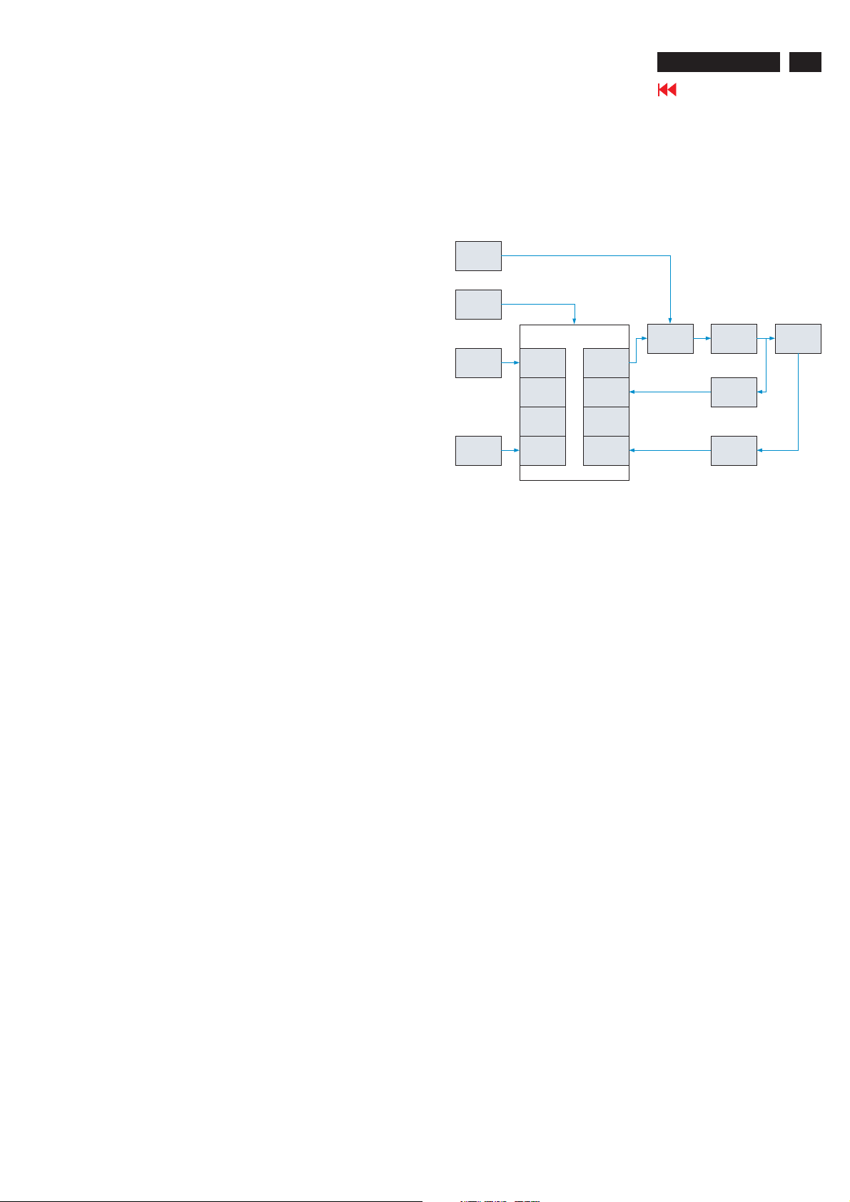
Power Board Block Diagram
Rec. & FilterLine Fil ter
PWM
Power
Transformer
Driver
Feedback
1.2 Inverter Circuit:
This unit operates on an output voltage of 22V given by
power source.
2.1 VDD:
1.
R105 gets a +5VDC for I101 power supply.
1.2.2 Control IC, I101 (OZ9938):
1.2.2a Enable:
When pin1 of I101 is over 2V, I101 is
initialized. If it is lower than 1V, the I101
turns off.
Output Rec. &
Filter
Page 4
1. Circuit Description (continued)
HP L1908W
Go to cover page
3
1.2.2b OSC:
When I101 enabled, C104, R118, R107 (pin13
of I101) determine the operating frequency.
1.2.2c SST:
C106 (pin12 of I101) provides soft start
function.
1.2.2d Ignition:
IC provides higher operating frequency
internally for more striking voltage until
regulation of feedback of lamp current. And it
provides 2 second striking time.
1.2.2e Dimming control:
The external PWM voltage of R136 and C111
control the duty pulse of burst-mode to drive
and perform a wide dimming control for the
CCFL. The burst-mode frequency is
determined by scaler IC.
1.2.2f Regulation:
Pin5 of I101 provides regulation of the CCFL
current from feedback. The non-inverting
reference is at 1.25V nominal.
1.2.2g Protection:
Open-lamp protection in the ignition period is
provided through pin6 of I101. Removal of the
CCFL during normal operation will trigger IC to
turn on and shut off the inverter. This is latch
function.
1.2.2h Output drivers:
The configuration prevents any shoot-through
issue associated with bridge-type power
conversion applications. Adjusting the overlap
conduction between Q104, Q105, the CCFL
current regulation is achieved.
1.2.3 Half-bridge Switching and Transformer:
Q104, Q105, C122, C123, C134 compose half-bridge
switching to convert DC into AC for driver the CCFL.
1.2.4 Detection:
C112, C114, C115, C116, C118, C119, R126, R116,
R115, R117, R119, R121, R122, R125 detect the
output voltage and ensure a rated voltage by pin6 of
I101 ensure not a open-lamp.
1.2.5 Feedback:
D116, D117, D120, D121, R111, R130 detect the
lamp current for negative feedback and
regulation.
Inverter Board Block Diagram
VCC
VDD
VDD
Half-bridge
Switching
ON/OFF
Brightness
Control
Control IC: OZ9938
Enable
OSC
SST
Dimming
Control
Output Driver
Protection
Ignition
Regulation
1.3 Interface Operation:
3.1 Top (Circuit diagrams sheet 2 of 8):
1.
This page is function block. (1)Power, (2)VGA &
DDC interface, (3)Scaler
GM5726H (GM5766H),
(5) Key & panel interface, (6) Audio.
1.3.2 Power (Circuit diagrams sheet 3 of 8):
1.3.2a P301 connector:
A 5V power supply for LCD module, also
it is main power of interface board. A VDD
(+5V) power supply for audio AMP. It is
generated from the P301 connector. And
adjust back light of LCD module from I306
scaler control.
GM5726H (GM5766H)
1.3.2b I302, 3-terminal regulator:
A 3.3V power supply for I306 scaler IC
GM5726H (GM5766H)
and I309 SPI flash ROM, it is generated
from the 5V source.
1.3.2c I303, 3-terminal regulator:
A 1.8V power supply for I306 scaler IC
GM5726H (GM5766H)
from the 3.3V source (I302).
Transformer Lamp
Detection
Feedback
and I308 EEPROM
, it is generated
Page 5

4
HP L1908W
Go to cover page
1. Circuit Description (continued)
1.3.2d Q302, I301:
The circuitry is functions of ON/OFF control
capable of initial the LCD module power on or
shut its power off (PANELVCC_EN) is
performed for power ON/OFF and also for the
power saving sequence. It supports 5V to
LCD module power. The PANELVCC_EN
signal is generated from I306 scaler IC
GM5726H (GM5766H)
1.3.2e R305:
ON/OFF control for LCD module back light
power ON/OFF control (BKLT_EN) is
performed for black light power ON/OFF and
also for the power saving sequence. The
BKLT_EN signal is generated from I306
scaler IC
3.2f Q301, R301, R302, R304:
1.
Adjusting backlight luminance of LCD
module, it s adjusted back light luminance
control (BKLT_ADJ) is performed for the back
light luminance. The BKLT_ADJ signal is
generated from I306 scaler IC
(GM5766H)
1.3.3 VGA & DDC interface (Circuit diagram sheet 4 of 8):
This sheet has RGB analog video and H/V sync
signals input from VGA connector.The RGB analog
video signals input through AC-coupled, analog
video signal is used to clamp the black level at 0V.
And H/V sync to scaler. Support EDID plug & play
function for analog video. It is to support VESA
DDC/CI interface for analog video.
1.3.3a P302 connector:
The RGB analog video and H/V sync input
signals to I306 scaler Gm5726H (Gm5766H).
The VESA DDC/CI function is through IIC bus
to I306 scaler IC .
1.3.3b I304, EDID EEPROM (24LC02B):
The I304 is support EDID information of the
VESA standard for VGA interface and support
plug and play for the PC host.
1.3.4 DVI & DDC interface (Circuit diagrams sheet 5 of 8):
The digital video signals (TMDS) input from P303
DVI-D connector. The digital video signal is TMDS
for DVI V1.0 standard. And support EDID plug&play
function for digital video. It supports VESA DDC/CI
interface, and support HDCP function.
.
.
.
GM5726H
GM5726H (GM5766H)
1.3.4a P303 connector:
P303 is DVI-D connector for DDWG standard,
it has digital video signals (TMDS) to I306
scaler IC . The VESA
DDC/CI function is through I2C bus to I306
GM5726H (GM5766H)
function is also through IIC bus to I306.
1.3.4b I305, EDID EEPROM (24LC02B):
The I305 is support EDID information of the
VESA standard for DVI interface, and support
plug & play for the PC host.
1.3.5 Scaler IC (Circuit diagram sheet 6 of 8):
The I306 is all-in-one LCD
monitor controller. It leverages Genesis patented
advanced image-processing technology as well as a
proven integrated ADC/PLL. Furthermore, it
integrates HDCP function, a micro-controller, an
OSD controller, and dual LVDS.
The RGB analog video signal from video input circuit
enter to incorporated A/D converted block (ADC) into
the digital data for analog video signal. The TMDS
digital signals input (with HDCP) entered from the
DVI-D connector is converted into the digital data.
Based on this conversion, this device performs
interpolation during pixel extension. These
interpolation digital data are transformed to LVDS
signal. The I306 source voltage is 3.3V and 1.8V, the
device clock source frequency is 14.318 MHz. And
support DDC/CI interface of VESAand function key
operation.
3.5a I308 EEPROM (24LC16B):
1.
1.3.5b I309 SPI Flash ROM:
1.3.5c I307 Microprocessor Supervisory Circuit:
GM5726H (GM5766H)
The control data and parameter, and OSD
related setting, and other service data, to be
stored in I308. The contents of which are
updated as required.
The firmware program running from I309
external SPI flash ROM, contains firmware
code and data for all firmware function. The
device is 2Mbits of flash ROM.
The function of this device is to assert a reset
to I306 scaler GM5726H (GM5766H), when
either the power supply dropped down.
GM5726H (GM5766H)
. And it supports HDCP
Page 6

1. Circuit Description (continued)
HP L1908W
Go to cover page
5
1.3.5d X301 14.318MHz:
It generates reference clock input for I306
scaler.
1.3.5e ISP and DDC/CI function:
The DDC/CI is VESA standard for the host PC
system, it can through I2C bus to control LCD
monitor. Enter I306 pin64 DDC_SCL_A and
pin65DDC_SDA_A of the VGA port. Enter I306
pin66 DDC_SCL_D pin67 DDC_SDA_D of the
DVI-D port. It use ISP function when change
new firmware to I309 SPI flash ROM, it used
IIC bus from VGA or DVI-D port through I306
to I309 SPI flash ROM.
1.3.5f The power save sequence function:
First I306 pin49 (BKLT_EN) set Low to disable
LCD module back light power, delay of some
time, then I306 pin127 (PANELVCC_EN) set
Low to disable LCD module power, then I306
enter to power down mode.
1.3.6 Key & Panel interface (Circuit diagrams sheet 7of 8):
1.3.6a P306 connector:
It is LVDS bus, it is from I306 scaler to LCD
panel module. The P306 output voltage is 5V.
1.3.6b P307 and P308 connector:
The P307/P308 has support keypad function.
Control is given effect for the push switch to be
used when the user changes the parameters,
in order to modify the respective setting
values. Whether the switch has been pressed
is identified with the switch input level change
of I306. Relate ports of I306 based on Table 1.
Each parameter is stored in the I308EEPROM,
the contents of which are updated as required.
The P307 have LED Blue and Amber light, the
LED Blue signal from I306 pin126, and the
LED Amber signal from I306 pin125.
Table 1 Related ports of I306
Pin No. I/O Signal name Function Remarks
Pin 113 I KEY_POWER Soft power s witch input Power k ey
Pin 115 I KEY_MENU Enter OSD s witc h input Enter O SD menu
Pin 114 I KEY_UP Switch input Up key or Viewing model selection
Pin 115 I KEY_DOWN Switch input Down key or Volume control of audio func tion
1.3.7 Audio (Circuit diagrams sheet 8of 8):
1.3.7a P309 connector:
The P309 is audio signal input from the audio
source.
1.3.7b P310 connector:
The P310 is audio output to speaker and
support 2Wx2speakers.
1.3.7c I310 TPA6021A4:
The I310 is 2x2W stereo audio amplifier, it is
an integrated class-AB dual output amplifier.
1.3.7d Q309:
Power down and mute control for Audio
ON/OFF control (AUDIO_EN) is performed for
standby mode and mute function. It supports
5V to audio IC power. The AUDIO_EN signal is
generated from I306.
1.3.7e R394, Q310, volume control for Audio:
Volume control (volume) is performed for
audio output signal power. The volume signal
is generated from I306.
1.3.8 Others:
1.3.8a Detection of POWER ON status:
The I306 is identified the ON status of two
modes for the power supplies. The
identification is made when the power supply
is turn off. For example, if the power supply is
turn off with the POWER key switch, the
POWER key switch must be turn on when
active the power supply again. If the power
supply turned off by the pulling out the power
cord, then this power supply can to be turned
on by connecting the power cord, without
pressing the POWER key switch.
1.3.8b Display mode identification:
(1) Display mode identification:
The display mode of input signal is
identified based on Table 2. When the
mode has been identified through the
measurement of horizontal and vertical
frequencies, the total number of lines is
determined with a formula of Horizontal
frequency and Vertical frequency=Total
number of number of lines . Final
identification can be made by examining
the coincidence of the obtained figure with
the number of lines for the mode identified
from the frequency.
Page 7
6
HP L1908W
1. Circuit Description (continued)
Go to cover page
The Distinction Hsync and Vsync of each mode is
shown in Table3. When the detected frequency if the
sync signal has changed, the total number of lines
should be counted even through it is range identified
frequency in the same mode.
(2) Out of range:
This out of range mode is assumed when the frequency
out of the horizontal/vertical signal is as specified
below.
Vertical frequency : 50 ~ 76 Hz.
Horizontal frequency : 24 ~ 83KHz.
(3) Power save mode:
The power save mode is assumed when the horizontal
and vertical signals are as specified below.
- If there is no horizontal sync signal input
- If there is no vertical sync signal input.
- If the horizontal sync signal is outside the measuring
range of I306.
- If the vertical sync signal is outside the measuring
range of I306.
Table 3 the Hsync,Vsync distinction
Indication
resolution
640 x 480
640 x 480
720 x 400
800 x 600
800 x 600
832 x 624
1024 x 768
1024 x 768
1152x720
1152 x 870
1152 x 900
1280x768
1280x960
1280 x 1024
1280 x 1024
1440x900
Distinction Hsync Distinction Vsync The fixed
30.5KHz≦fH≦32.5KHz 59Hz≦fV≦61Hz
36.5KHz≦fH≦38.5KHz 74Hz≦fV≦76Hz
30.5KHz≦fH≦32.5KHz 69Hz≦fV≦71Hz
36.9KHz≦fH≦38.9KHz 59.3Hz≦fV≦61.3Hz
45.9KHz≦fH≦47.9KHz 74Hz≦fV≦76Hz
48.7KHz≦fH≦50.7KHz 73.5Hz≦fV≦75.5Hz
47.4KHz≦fH≦49.4KHz 59Hz≦fV≦61Hz
59KHz≦fH≦61KHz 74Hz≦fV≦76Hz
43.9KHz≦fH≦45.9KHz 59Hz≦fV≦61Hz
67.7KHz≦fH≦69.7KHz 74Hz≦fV≦76Hz
70.7KHz≦fH≦72.7KHz 75Hz≦fV≦77Hz
46.4KHz≦fH≦48.4KHz 59Hz≦fV≦61Hz
59KHz≦fH≦61KHz 59Hz≦fV≦61Hz
62.9KHz≦fH≦64.9KHz 59Hz≦fV≦61Hz
79KHz≦fH≦81KHz 74Hz≦fV≦76Hz
55KHz≦fH≦57KHz 59Hz≦fV≦61Hz
1.3.8c Power ON sequence
When the POWER key switch is pressed, the
POWER key switch signal is turned H . When this
H potential is detected, the CPU begins to
establish the respective power supplies according
to the sequence show below.
mode
1
2
3
4
5
6
7
8
9
10
11
12
13
14
15
16
Table 2 video model
Band W idth
(KHz )
1 640x480 (59. 94Hz) 31.469 25.175 - -
2 640x480 (75Hz) 37.5 31.5 - -
3 720x400 (70Hz) 31.469 28.322 - +
4 800x600 (60Hz) 37.879 40 + +
5 800x600 (75Hz) 46.875 49.5 + +
6 832x624 (74. 55Hz) 49.722 57.284 +/- +/-
7 1024x768 (60Hz) 48.363 65 - -
8 1024x768 (75Hz) 60.023 78.75 - -
9 1152x864 (60Hz) 44.86 66.75 - +
10 1152x870 (75Hz) 68.68 100 +/- +/-
11 1152x900 (65Hz) 61.80 92.978 +/- +/-
12 1280x768 (60Hz) 47.396 68.25 + -
13 1280x960 (60Hz) 60.00 108.00 +/- +/-
14 1280x1024 (60Hz) 63.981 108 + +
15 1280x1024 (75Hz) 79.976 135 + +
16 1440x900 (60Hz) 55.94 106.5 - +
(M H z)
Po lar ityM o d e Reso lu tio n H-F r eq
HV
Power Key
296ms
LED Green
PANELVCC_EN
BKLT_EN
AUDIO_EN
516ms
825ms
3.68s
1.3.8d Power OFF sequence:
When the POWER key switch is pressed, while the
power supply is ON, the POWER key switch signal
is turned H . When this H potential is detected,
the CPU begins to turn off the respective power
supplies according to sequence show below.
Power Key
140ms
LED Green
460ms
PANELVCC_EN
157ms
BKLT_EN
AUDIO_EN
140ms
Page 8

1. Circuit Description (continued)
HP L1908W
Go to cover page
7
1. 3.8e List of I/O Pin Assignments of the I306:
Pin No. Port Signal Name
113 LBADC _IN3 PWR_KEYn H O N/OF F LCD monitor
126 GPIO14 LED_B L LED Blue enable when is H
125 GPIO13 LED_A L LED amber enable when is H
114 LBADC _IN2 KEY_UPn H OSD up/plus enable when is 2.46V
115 LBADC _IN1 KEY_MENUn H OSD enter enable when is 2.46V
115 LBADC _IN1 KEY_DO WNn H O SD down/ minus enable when is 2.0V
86 GPIO31 HDCP_HPDn L DVI HPD enable when is L
122 G PIO10 SC L H EEPR OM cloc k signal of IIC bus
123 G PIO11 SD A H EEPROM data signal of IIC bus
50 GPO4 BKLT_ADJ - Backlight br ightnes s control
124 G PIO12 D DC_WPn L DDC EEPROM write p rotect ion when is L
51 GPO0 AUDIO_EN L Audio enable when is H
56 GPO1 VOLUME L Audio v olume
121 GPIO9 VG A_DETn H VGA cable c onnected when is L
120 GPIO8 DVI_DETn H DVI cable connec ted when is L
58 GPO3 UART_DO H UART interface data O UT
57 GPO2 UART_DI H UART interface dat a IN
127 PPWR PANELVCC_EN L Panel power enable when is H
49 PBIAS BKLT_EN L Back light power enable when is H
64 GPIO16 DDC_SCL_VGA H DDC/CI interfac e for VGA
65 GPIO17 DDC_SDA_VGA H DDC/ CI interface for VG A
66 GPIO18 DDC_SCL_DVI H DDC /CI interface for D VI
67 GPIO19 DDC_SDA_DVI H DDC/CI interface for DVI
Initial
Setting
Function
1.3.9 Miscellaneous:
1.3.9a Connector Pin Assignments:
VGA Analog Connector Pinout
PIN MNEMONIC SIGNAL
1 RV Red Video
2 GV Green Video
3 BV Blue V ide o
4 NC None
5 GND Ground (DDC Return)
6RG RedGND
7 GG Green GND
8BG BlueGND
9 +3.3/+5 V +3.3/+5 V (from PC)
10 SG Sync Ground
11 NC None
12 SDA DDC Data
13 HS Horizontal Sync
14 VS Vertical Sync
15 SCL DDC Clock
1.3.9b LED Indicator:
Full Power - HP branded models Green
Sleep - all models Amber
Sleep Timer activated Sleep Mode Flashing Amber (0.5 Hz)
1.3.9c Factory Preset Display Modes:
V-
Pola rit y
Pix el Cl k
(MHz)
Source
CVT 0.83MA
DVT 16:10
Preset
NOTE: Modes 13 thru 15 are support ed with scaled down video pri mari ly t o support navigat ion
to a support ed ti ming mode.
Pix el
Format
1 640 x 480 31. 47 - 59.94 - 25.175 VGA
2 640 x 480 37. 5 - 75 - 31. 5 VGA
3 720 x 400 31. 47 - 70.08 + 28. 321 VGA
4 800 x 600 37. 88 + 60. 32 + 40 VESA
5 800 x 600 46. 88 + 75 + 49.5 VESA
6 832 x 624 49. 72 74.55 57.283 MAC
7 1024 x 768 48.36 - 60 - 65 VESA
8 1024 x 768 60.02 - 75. 03 - 78. 75 VESA
9 1152 x 720 44.86 - 60 + 66.75
10 1152 x 870 68.68 75.06 100 MAC
11 1152 x 900 61.8 65.96 92.978 SUN
12 1280 x 768 47.396 + 60 - 68.25 CVT 0.98M9-R
13 1280 x 960 60 60 108 VESA
14 1280 x 1024 63.98 + 60.02 + 108 VESA
15 1280 x 1024 79.98 + 75.02 + 135 VESA
16 1440 x 900 55.94 - 59. 89 + 106.5 CVT 1. 30MA
H-Fr eq
(kHz)H-Pola rit y
V-Fr eq
(Hz)
PI N 1
PI N 11
PI N 5
PI N 9
Page 9
8
HP L1908W
Go to cover page
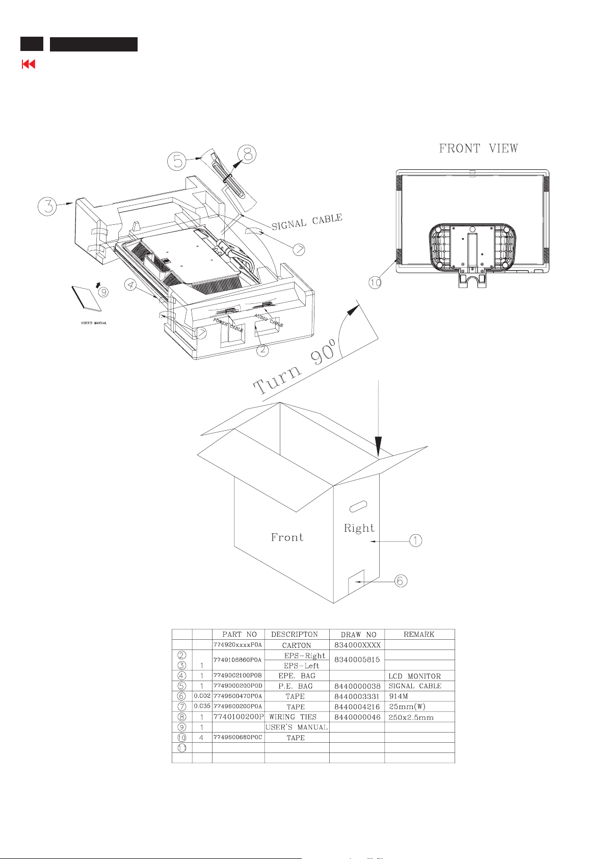
2. Packing Exploded Drawing
The Pape r m ust on top of USER'SMANUAL
in orde r to p ro t ect M ANU AL
.
Page 10
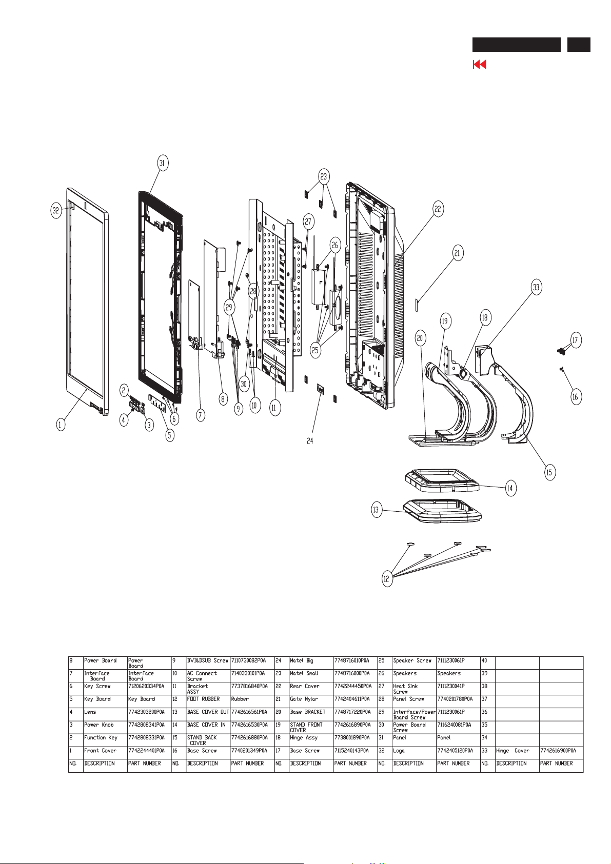
3. Product Exploded Drawing
HP L1908W
Go to cover page
9
Page 11
10
HP L1908W
Go to cover page
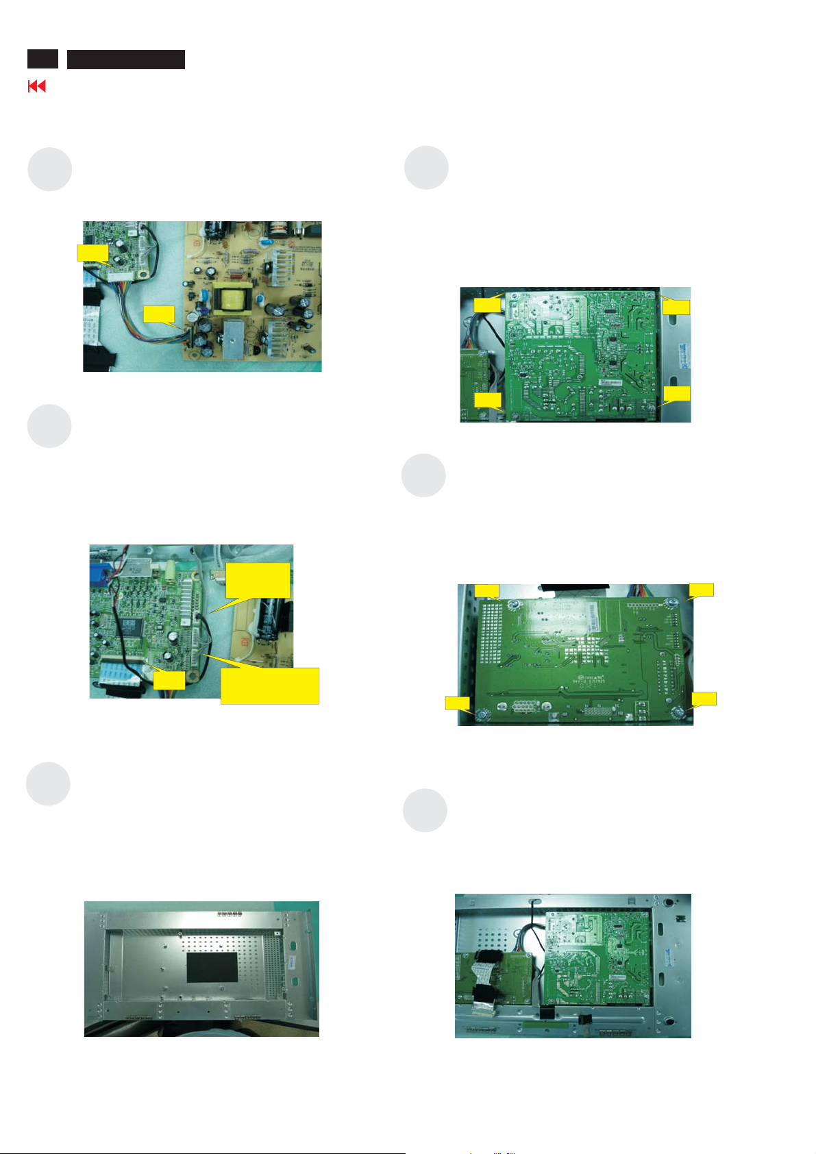
4.1 Assembly Procedures:
Connect the cable between power board(P802) and
S1
interface board (P301)
P301
4. Assembly and Disassembly Procedures
Use a Phillips-head screwdriver screwed the No.1~4
S4
screws till that power board and bracket chassis base
firmly attached.
(No1 screw size=M4x8; No2~4 screw size=M3x6;
Torque=8~10KGFxCM).
S2
P802
Connect FFC cable into interface board
Connect function key cable into interface
board(P307)
Connect speaker cable into interface board(P310)
SPEAKER
CABLE
FFC
FUNCTION KEY
CABLE
S5
3
1
Use a Phillips-head screwdriver screwed the
No.1~4 screws till that interface board and bracket
chassis base firmly attached.
(No1~4 screw size=M3x6; Torque=8~10KGFxCM).
3
4
4
2
1
2
S3
Take a bracket chassis base on a protective
cushion and stick an insulator on the specific
position, take a power board and turn it over. Then,
put it on the specific positions of bracket chassis
base.
Use PVC tape to stick the speaker cable
S6
Page 12
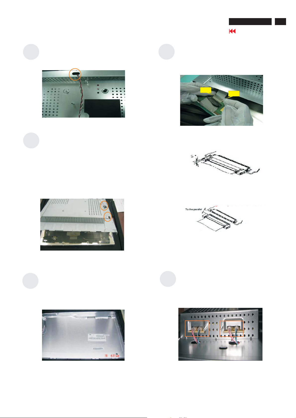
4. Assembly and Disassembly Procedures (continued)
HP L1908W
Go to cover page
11
Take the speaker cable out of the hole shown as
S7
photo
Turn the monitor faced down and put it on the
S8
Bracket Chassis module till both parts firmly
attached
Take lamp cables out from the holes shown as the
photo.
S10
Connect FFC cable to LCD panel. There are two
locks over here when plugging in should be
noticed
LOCK
LOCK
Plug in parallel direction
S9
Connect the FFC cable to the connector of the LCD
panel.
S11
Angel < 5 degrees
Plug 8 lamp cables to the connectors of power
board.(Both of right and left sides)
Page 13
12
HP L1908W
Go to cover page
4. Assembly and Disassembly Procedures (continued)
S12
S13
Use a Phillips-head screwdriver screwed the No.1~4
screws on both side and assemble the LCD panel
and bracket chassis module.
(No1~4 screw size=M3x5; Torque=2.5~3KGFxCM).
1
3
Use a Phillips-head screwdriver screwed the
No.1~2 screws.
(No1~2 screw size=M3x10; Torque=4~6KGFxCM).
1
2
4
2
S16
S17
Connect function key cable into key function cable
(P600)
Put the previous assembled module on the front bezel
Use a Phillips-head screwdriver screwed the
No.1~4 screws.
No1~4 screw size=M2x3.3Torque=0.8~1.2KGFxCM
34
2
1
S14
S15
Use a Hex-head screwdriver screwed the
bracket chassis
(No.1~4 Hex Nut screws
Size=M3x8;Torque=5~7KGFxCM).
12
4
Use a Phillips-head screwdriver screwed the bracket
chassis No.1 screw.
(No1 screw size=M3x4; Torque=4~6KGFxCM).
1
3
S18
S19
Use a Phillips-head screwdriver screwed the
No.1~4 screws.
(No1~4 screw size=M3x6; Torque=6~8KGFxCM).
2
3
Fix speaker line with hook shown as photo
1
4
Page 14

4. Assembly and Disassembly Procedures (continued)
HP L1908W
Go to cover page
13
S20
S21
Put a rear cover on the assembled unit and press
on force mechanisms locked and firmly attached.
4
3
2
1
4
3
2
1
Assemble the stand upper side to the rear cover
through the way of screwing 3 screws till both
units firmly attached.
(No1~2 screw size=M4x14; No3 screw
size=M4x10; Torque=11~13KGFxCM).
1
2
S24
S25
Take two cushion foams; one is held the right side
of LCD monitor, and another is held the left side.
Put accessories f VI able nd
pcos pb
ower able n pecific positions as hoto elow
o D c audio cable a
,
DVI CABLE
POWER
.
S22
S23
3
Stick a screen card on the front bezel with four
tapes.
3
4
1
2
Cover the finished good with an EPE bag. Stick
the EPE bag with one adhesive tape on the rear
side.
S26
AUDIO
CABLE
Move previous assembled parts into the carton
then packing the carton
Page 15

14
HP L1908W
Go to cover page
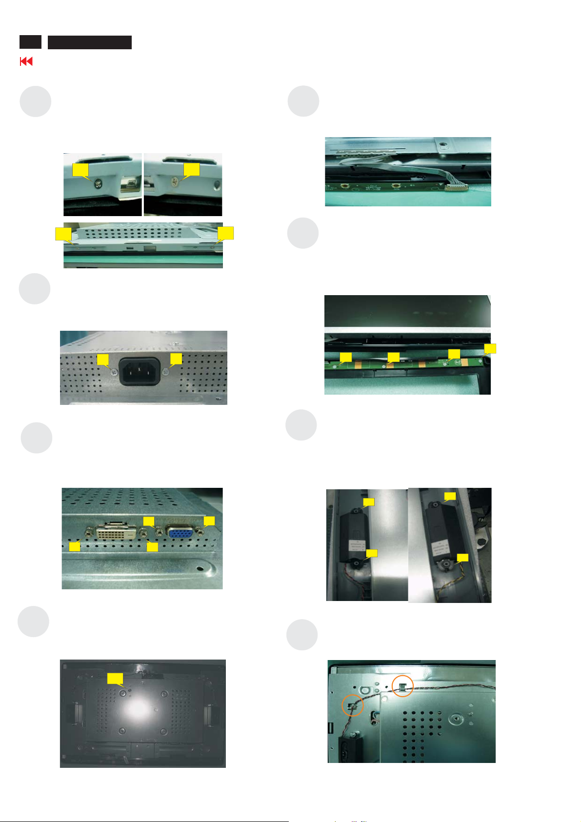
4.2 Disassembly procedures
4. Assembly and Disassembly Procedures (continued)
S1
S2
Open the carton with a proper tool.
Take out all accessories including power cable, DVI
cables, audio cable and packing material from the
carton.
(Note: It depends on whether users returning the
accessories.)
DVI CABLE
POWER
S5
S6
Use a Phillips-head screwdriver unscrew 3 screws to
release the stand base.
(No1~2 screw size=M4x14; No3 screw size=M4x10;
Torque=11~13KGFxCM).
1
Turn over the LCD monitor (screen faced up).
2
3
S3
S4
AUDIO
CABLE
Take off two cushion foams
ut returned unit on a protective cushion,then
P
remove LDPE+EPE bag.
S7
Place cloth on the panel where you are working
on to protect the panel. Continuously, wedge
your finger between the front bezel and the panel,
then pry up on the front bezel to disengage the
locking mechanism.
Work your way along the front bezel to disengage
all the locking mechanism.
Page 16

4. Assembly and Disassembly Procedures (continued)
HP L1908W
Go to cover page
15
Turn over the LCD module(screen face down) then
S8
remove the rear cover
Use a Phillips-head screwdriver unscrewed
S9
number 1~4 screws to release the power key board
from the front bezel
No1~4 screwsize=M2x3.3 Torque=0.8~1.2KGFxCM
S11
S12
Use a Phillips-head screwdriver unscrewed number
1~2 screws to release the speaker from the front
bezel
(No1~4 screw size=M3x6; Torque=6~8KGFxCM).
2
3
1
4
Use a Hex-head screwdriver unscrewed 4 screws to
release the D-SUB and DVI connectors
(No.1~4 Hex Nut screws
Size=M3x8;Torque=5~7KGFxCM).
12
S10
34
2
1
Unconnect the function key cable then remove the
front bezel
S13
S14
4
3
Use a Phillips-head screwdriver unscrewed the
No.1~2 screws to lease power plug
(No1~2 screw size=M3x10; Torque=4~6KGFxCM).
1
2
Use a Phillips-head screwdriver unscrewed the
No.1~4 screws to disassemble the LCD panel and
bracket chassis module.
(No1~4 screw size=M3x5; Torque=2.5~3KGFxCM).
1
3
2
4
Page 17

16
HP L1908W
Go to cover page
4. Assembly and Disassembly Procedures (continued)
S15
S16
Use a Phillips-head screwdriver unscrewed the
No.1screws to lease power plug
(No1 screw size=M3x4; Torque=4~6KGFxCM).
1
Unplug 4 lamp cables (No. 1~4).
S18
S19
Disconnect the FFC cable to the connector of panel.
Use finger to push the lock according to arrow
direction then take out the FFC cable
LOCKLOCK
Examine the panel surface accoring to inspection
criteria. Put it aside.
S17
Take out lamp cables right through the No.1 and
2 square holes and separate the bracket chassis
module and LCD panel apart.
1
2
S20
Use a Phillips-head screwdriver unscrewed the
No.1~4 screws to release the interface board.
(No1~4 screw size=M3x6; Torque=8~10KGFxCM).
3
4
1
2
Page 18

S21
4. Assembly and Disassembly Procedures (continued)
Use a Phillips-head screwdriver unscrewed the
No.1~4 screws to disassemble the power board.
(No1 screw size=M4x8; No2~4 screw size=M3x6;
Torque=8~10KGFxCM).
HP L1908W
Go to cover page
17
S22
3
1
4
2
Disconnect FFC cable into interface board
Disconnect speaker cable into interface board
Disconnect function key cable into interface board
SPEAKER
CABLE
FFC
FUNCTION KEY
CABLE
S23
Disconnect the cable between power board(P802)
and interface board (P301)
P301
P802
Page 19

18
HP L1908W
5. Troubleshooting
Go to cover page
5.1 No display on the screen (screen is black, and colour of LED is amber.):
Does the OSD display
on the screen upon pressing
the ‘MENU’?
YES
Check if the sync
signal from computer is
output and if the video cable is
firmly connected.
OK
Proceed to ’5.4 Abnormal screen’
section.
Proceed to ’5.5 Abnormal OSM display’ section.
NG
Input the sync signal of computer or change to
NG
other workable cable for cross-test.
Page 20

5. Troubleshooting (continued)
5.2 Nothing displays on the screen (Screen is black, colour of LED is green.):
HP L1908W
Go to cover page
19
Is backlight lite? Proceed to ‘5.3 Checking the backlight unit’ section
OK
Does the connected
computer output RGB
video signals?
OK
Check the OSD
menu whether if be shown on
the screen upon pressing the
"MENU" key.
OK
Proceed to ‘5.4 Abnormal Screen’
section.
NG
NG
NG
1) Change pattern of video signal output on the host.
2) Reconnect the video cable.
3) Change the video cable.
Check if the LCD
video signal cable is connected
properly between the MAIN
PWB and LCD module.
The cable is disconnected.NG
Check if the 3.3V
power is supplied on I302, pin2
and the 1.8V power is supplied
on I303, pin2.
OK
Check all LVDS signal
pins, output from I306.
OK
Failure Point
1) The cable broke between P306
and LCD module.
2) LCD module failure.
OK
NG
NG
Failure Point
Printed wire broke or shorted
between I306 and P306.
on I302, pin3 that is high level
Check if the Vdc
DC at 5V.
OK
Failure Point
I302 is defected.
NG
Failure Point
1) Printed wire broke between
P301 pin1, pin2, pin3 and I302.
2) Check power board.
Page 21

20
HP L1908W
Go to cover page
5.3 Checking the backlight unit:
5. Troubleshooting (continued)
Check the BKLT_EN
signal of the rectangle input
P301 pin 2 at TTL
high level
OK
Check if the input
signal from the I306 pin50 is a
DC voltage.
OK
Failure Point
Inverter of power board is defected.
Proceed to ‘5.11 Checking the
backlight unit’ section
NG
NG
Is a "H" level been
output in the TTL level from I306
pin49? <or> Is a ‘BKLT_EN’ signal of
the rectangle been
output?
Failure Point
1) Printed wire broke between I306
pin50 and P301.
2) I306 failure.
NG
Failure Point
Printed wire is broken between
I306 pin49 and P301.
Page 22

5.4 Abnormal screen:
Check the R, G, B video
signal from computer input on DSub
R, G, B connector.
5. Troubleshooting (continued)
NG
1) No R, G and B video signal is output from the
connected computer. Contact your regional computer
supplier for technical support.
2) Video signal cable is disconnected.
Failure Point
HP L1908W
Go to cover page
21
OK
Check the R, G, B
input signals on I306 pin93, pin96,
pin99 respectively that their level is
0.7Vp-p maximum.
OK
Check all LVDS signal pins
which are output from I306.
OK
Process ‘5.8 Checking the resolution change
IC movement’ section.
NG
NG
Failure Point
Below results are based on the Red signal. (Green and
Blue signals are the same.)
1) Printed wire is broken between D-Sub(R) and I306
pin99.
2) R315 is short.
3) C317 is open.
4) R310 is open.
5) FB305 is open
6) FB306 is open
Failure Point
1) I306 failure.
2) Printed wire is broken between I306 and P306.
Page 23
22
HP L1908W
5. Troubleshooting (continued)
Go to cover page
5.5 Abnormal OSD screen, OSD adjustment problem:
Check the input TTL level
whether if it was changed upon
pressing function keys.
OK
Proceed ‘5.4 Abnormal Screen’ section.
NG
Failure Point
1) Printed wire broke between P308 pin 5 and I306 pin 113.
2) Printed wire broke between P308 pin 4 and I306 pin 113.
3) Printed wire broke between P308 pin 3 and I306 pin 113.
4) Printed wire broke between P308 pin 2 and I306 pin 113.
5) C389, C390, C391, C392, short.
6) R381, R382, R384, R385, R378, R379 short/open.
7) R380, R383 open.
8) I306 failure.
Page 24

5.6 Abnormal plug and play operation:
5.6.1 Abnormal DDC2 (D-SUB):
5. Troubleshooting (continued)
HP L1908W
Go to cover page
23
Confirm the output
of serial data on I304 pin 6
synchronize SCLK at
TTL level.
OK
Failure Point
1) The host machine isn't communicating in DDC2
mode.
2) The video cable may be defected or may be
disconnected to cause the DDC communication
failure.
3) Printed wire is broken between I304 pin6 and P302
pin15.
4) R328, R329 is open.
5) I304 pin5 or pin6 is short.
6) Video cable is defected.
5.6.2 Abnormal DDC2 (DVI):
Failure Point
NG
I304 is defected.
Confirm the output
of serial data on I305 pin6
synchronize SCLK
at TTL level.
OK
Failure Point
1) The host machine isn't communicating in DDC2
mode.
2) The video cable may be defected or may be
disconnected to cause DDC communication
failure.
3) Printed wire is broken between I305 pin6 and P303
pin6.
4) R346, R347 is open.
5) I305 pin5 or pin6 is short.
6) Video cable is defected.
Failure Point
NG
I305 is defected.
Page 25

24
HP L1908W
5. Troubleshooting (continued)
Go to cover page
5.7 Checking the interface circuit of sync signal:
5.7.1 Checking the control circuit of horizontal sync pulse:
Check the
Horizontal sync
signal on I306 pin89
TTL level.
OK
Proceed to ‘5.8 Checking the resolution
change IC movement’ section.
NG
Failure Point
1) Video cable may have failed.
2) Printed wire broke between P302 pin13 and I306
pin89.
3) FB311, R321 is open.
4) R324, C328 is short.
5) I306 is defected.
5.7.2 Checking the control circuit of vertical sync pulse:
Check the vertical
sync signal on I306
pin90 TTL level.
OK
Proceed to ‘5.8 Checking the resolution
NG
change IC movement’ section.
Failure Point
1) Video cable may be defected.
2) Printed wire is broken between P302
pin14 and I306 pin90.
3) FB312, R322 is open.
4) R323, C327 is short
5) I306 is defected.
Page 26

5.8 Checking the resolution changed IC movement:
5. Troubleshooting (continued)
HP L1908W
Go to cover page
25
on I306 pin2, pin25, pin47, pin53, pin74,
Is there +3.3V supply
pin82, pin91, pin92, pin101, pin110,
pin116?
OK
Is there +1.8V supply on I306
pin17, pin55, pin70, pin78, pin87,
pin104, pin106, pin118?
OK
Is 14.318MHz clock input
to I306 pin108 and pin109 at TTL
level during Power On?
OK
NG
NG
Proceed ‘5.9 Checking the DC/DC converter circuit’
section.
Proceed ‘5.9 Checking the DC/DC converter circuit’
section.
Is 14.318MHz clock
output from X301 pin1 at
NGNG
TTL level during Power
On?
Failure Point
OK
X301 failure
Failure Point
Is +5.0V supplied to I306 pin111 at
low level (Reset signal)?
OK
Failure Point
I306 is defected.
Print wire broke between X301
pin1 and I306 pin108.
NG
Check if the output of 5.0V
"L" pulse from I307 pin 2.
OK
Failure Point
Print wire broke between I307
pin2 and I306 pin111.
NG
Is 5.0V supplied to I307
pin3?
OK
Failure Point
I307 is defected.
Page 27

26
HP L1908W
Go to cover page
5.9 Checking the DC/DC converter circuit:
5. Troubleshooting (continued)
Check if the 5V is output
from P301 pin5, pin6 to I302 pin3.
Take off wire harness
connector of P301. Check if the
output of +5.15V between P802 +5.1V
(whichever pin 4,5,6,7) and ground (The
through hole of power board).
NG
Failure Point
Power board defect, proceed to
“5.10N0powerONcheck.”
NG
OK
Does +3.3V on I302 pin 2?OK Does +1.8V on I303 pin 2?OK
NG
Is the low resistance
(lower than 5? ) between I302
pin 2 and ground
(P301 pin 1 or pin 9) ?
Yes
Failure Point
1) I302 defected.
2) The +3.3V circuit been ground
connection.
* Might be I306 defected or by pass
capacitor of power pin of I306 3.3V
defect.
NG
Is the low resistance
(lower than 5? )
between I303 pin 2 and ground
(P301 pin 1 or pin 9) ?
Yes
Failure Point
1) I303 defected.
2) The +1.8V circuit been ground
connection.
* Might be I306 defected or by pass
capacitor of power pin of I306 1.8V
defect.
Is the low resistance
(lower than 5 ohm)
between I302 pin3 and ground
(P301pin1orpin9)?
No
Is the low resistance
(lower than 5 ohm) between
I302 pin2 and ground
(P301 pin1 or pin9)?
Yes
Failure Point
1) I302 defected.
2) The +3.3V circuit been ground
connection.
* Might be I306 defected or by pass
capacitor of power pin of I306 3.3V
defect.
Yes
Failure Point
1) C313 short.
2) I302 is defected.
No
Failure Point
1) I302 is defected.
2)Printed wire is broken between I302
pin3 and output of FB301,FB302.
Page 28

5.10 No power on:
Check if the output voltage
+5V is correctly
OK
6. Troubleshooting (continued)
Failure Point
OK
The functions of Power Board is working
successfully.
HP L1908W
Go to cover page
27
Check if AC power
cord P801 and signal cables
of P302, P802, P101, P102,
P103, P104 is connected
properly.
OK
Check if C801 has
charged DC140V-330V
OK
Check if C807 is over
16V or not.
OK
Check if I801 pin8
has same pulse
or not.
Failure Point
Reconnect the P801, P302, P802, P101, P102,
NG
P103, P104 cables and make sure they are firmly
connected.
Failure Point
NG
Check F801, D802, P801 and repair them if be
damaged
Failure Point
NG
Check D803, R807, I801, C807, ZD801 and repair
them if be damaged.
Failure Point
NG
Check peripheral components of I801 and repair
them if be damaged.
OK
CheckifT801pin1has
same pulse or not.
OK
Check if peak voltage
of R813 triangle pulse is up to
1.5V or not.
OK
Check T801,
D812, C825, C824 have
same short circuit, or the
output +5V is
over load
OK
Check feedback circuit around I803 and
the other component and repair them if be
damaged.
Failure Point
NG
Check Q801, R813 and repair them if be damaged.
Failure Point
NG
Check if peak voltage of R813 triangle pulse is up
to 0.85V or not.
Failure Point
OK
Repair T801, D812, C825, C824 if be damaged.
Page 29

28
HP L1908W
Go to cover page
5.11 Checking inverter board circuit:
5. Troubleshooting (continued)
Check 22V output
pin is around 20V; on/off
pin is over 3V; brightness pin is in the
range o f 0V and
3.2V.
OK
Check if I101 pin6 is 5V.
OK
Check if P101, P102, P103,
P104 is connected properly.
OK
Check if I101 pin4, pin5 has triangle
pulse.
Failure Point
OK
The functions of Inverter Board is working successfully.
Failure Point
NG
Check R105, C112 and repair them if be damaged.
Failure Point
NG
Check CCFL and repair them if be damaged.
Failure Point
NG
Check I101 and repair them if be damaged.
OK
Check if I101 pin1 has
soft start edge up to 2.4V.
OK
Check if T801 pin1 has
same pulse or not.
OK
Check if I101 pin8
haspulseupto1.2Vfromoutput
detection.
OK
Check if half bridge
circuit (Q104, Q105, Q106, Q107,
Q108) is
working fine .
Failure Point
NG
Repair I101.
Failure Point
NG
Check Q801, R813 and repair them if be damaged.
Failure Point
NG
Check D102, D103, D107, D108, D114, D115, D112,
D113 and repair them if be damaged.
Failure Point
OK
Repair Q104, Q105, Q106, Q107, Q108 if be damaged.
OK
Check if transformers of T101, T102 are
working fine .
Page 30

5.12. Abnormal Audio Output:
Check if the audio signal supplied
to I310 pin 4,5,7 and 8.
5. Troubleshooting (continued)
NG
HP L1908W
Go to cover page
Failure Point
1) Check if audio cable is connected to P309.
2) Check if FB318, R386 or C394 open/short.
3) Check if FB319, R387 or C398 open/short.
4) Check if C395, C396 open/short.
2) Check if printed wire is broken between P309
pin2 (pin3) and C398 (C394).
3) Check if I310 defect.
29
OK
Check if the +5.35V is
Supplied to I310 pin 3, pin 6
and pin 9.
OK
Check if the logic H level on the
I310 pin 14.
OK
I306 defected.
Check if the lower than 0.5V
on the I310 pin 18 while volume
at default setting.
Failure Point
1) Check if FB321 defect.
2) Check if printed wire is broken between P301
pin7 (pin8) and FB321.
NG
3) Check if I310 defect.
* The circuit been ground connection on
pin3, pin6, and pin9.
NG OK
Failure Point NG
Yes
Check if the logic High level
on I306 pin 51.
NG
Check if the PWM pulse on
I306 pin 56.
Failure Point
1) Check if R390, R391, R392 open.
2) Check if C400 short.
3) Check if Q309 defected.
4) Check if printed wire is broken between Q309
and I310 pin14.
5) Check if I310 defect.
* The circuit been ground connection on pin3
or pin 6 or pin 9.
Failure Point
1) Check if R393, R394, R395, R396, C405
open/short.
2) Check if Q310 defected.
Yes
3) Check if printed wire is broken between Q310
and I306 pin 56.
5) Check if I310 defect.
NG
1) Check if printed wire is broken between I310
pin2, pin20, pin10, pin12, and P310 pin4, pin3,
pin2, pin1.
2) Check if I310 defect.
3) Check if wire harness is broken.
4) Check if the speaker defected.
Page 31

1234567 8910111213
G
F
E
Speaker
2x2W
D
To Speaker
P310 Audio Output
C
B
A
6. Schematics and Layouts:
.6 1 HP_L1908W_BLOCK DIAGRAM
AC IN-
1234567 8910111213
Audio
Source
P309 Audio Input
()AUDIO Source
DDC SCL DVI__
DDC SDA DVI__
()DVI EDID
I305 24LC02
I310 Audio AMP
()TDA6021A4
LDO
+.3 3V Main
Power
I303 I307 Reset IC
LDO
+5V DC power
I302
+5V DC power
for audio
Brightness Invter On Off,/
Power)
+5V DC Power
(Switch LCD
Panel
P301
()Connect to Power Board
Power Board
CCFL Wire
Video
Input
Video
Input
Digital
Analog
P303 DVI D-
P302 DSUB
TMDS
RGBHsVs,,, ,
()VGA EDID
DDC SCL VGA__,
DDC SDA VGA__
I304 24LC02
+.1 8V Main
Power
Power
Gm5726H
Scaler
I306
Serial Flash ROM
+.3 3V Main
I301
+5V Panel
Power
LVDS
P306 LVDS output
LCD Module
PCB No.
P307 P308&
Function Key Input
& LED output
Function
Key
Board
I309
EEPROM
24LC16B
I308
Interface Board
G
F
E
D
C
B
A
Go to cover page
HP L1908W
30
Page 32

G
F
E
D
C
B
A
._2 POWER BOARD6 _SCHEMATICSHP_L1908W
1234567 8910111213
R151 39K 75K:~
(. ~ . )7 5mA 6 5mA
VCC
GND 1-
P801
GND
R820
300K
0805
0 1U 275V./
C804
*
0 1U 275V./
C825
2200P 250V Y/-
GND 1-
0 01u 1KV./
2
D801
GBLA08
100U 450V/
GND
2
1
C809
N
0805
GND
15K
2
300K
+
1KV
R804
1
-
4
G
3
R821
300K
0805
C801
*
4
3
C819
C820
2200P 250V Y/-
+
C805
C815
0 01uF.
3 15AL250V.
R822
C803
ET 20-
3
L
1
T801
051.
F801
R802
SCK083
C808
0 01u 1KV./
R803
1234567 8910111213
GND 2-
R101
10K
C105
1000P
R135
1M
GND 2- GND 2-
1000P
C130
R151
39K
1000P
C131
GND 2-
GND 2-
GND 2-
1000P
GND 2-
2
2 2uF 50V./
30 1K.
R103
18K
GND 2-
876
NC
OVPT
VSEN
OZ9938
ENA
LCT
NC
9101112131415
C103
2 2uF 50V./
1
2
+
R106
150K 1%
C106
0 047uF.
C161
68P
C104
330P
C111
+
C110
R102
1
5
ISEN
DIM
SSTCMP
CT
R107
56K.
10K
4
GND 2-
R113
3
TIMER
GNDA
2
VDDA
DRV2
GND 2-
DRV1
PGND
GND
1
16
510K
56K
22uF 50V/
R104
R118
I101
10K
2
R136
0 1uF.
C101
C102
+
1
22
GND
R105
GND
GND
4 75K 1.%
23
R826
1K
R825
270
C827
GND 1-
R806
4
I802
1
R823
120K 0805/
R829
+5V
ON OFF-
BRI
R808
13K
GND 1-
33nF
C812
C826
10K
1uF 50V/
GND 1-
2 2uF 50V./
A
1
VR801
2
C828
I803
AP431
1
+
LTV817
+
C
2
1K
R
3
0 01uF.
R827
33K 1%
0
VCC
GND 1-
1uF 50V/
R816
0 22uF.
C813
R809
100K
1
2
+
C829
PRCT
CTRL
TEA1530
GDRV
IS
54
68K 0805/
R830
1K MOF/
R819
4 7K MOF./
R815
0 22uF.
C811
D807
18B
1
3
2
1
VCC
GND
I801
HV SPACE
DRAIN
8
7
6
82uF 35V/
GND 1-
C807
1
2
+
22 MOF/
R814
R813
100 MOF/
1N4148
D806
21
R807
39.
PCB No.
6832177300P01
GND
GND
2
2 1
0 022uF.
470 1%
D121
1N4148
D113
1N4148
C128
R130
1
GND
12K
21
21
1K 0805/
R128
D112 1N4148
21
GND
1N4148
R142
D120
D118
1N4148
GND
R122
15K 1%
100 0805/
1K 0805/
R126
33K1.%
470P
X7R
R140
R139
21
C119
2
2
1N4148
3M 1 4W/
R121
100K 1%
GND
D109
R125
MOF
100K 2W/
R818
C806
R805
1
C818
C817
0 1uF.
R840
D811
JUMPER WIRE
+
+
C814
1W
2 10
ER28
L804
3
2
1
+22V
T802
D809
STPF1020CT
1
1N4937
1
BEAD 6mm/
L803
SRF1045C
2
GND
GND
D804
21
7
3
D810
1K
1
2
3
7N65C
Q803
1KV X7R
R811
C832
3300P 250V/
0805
1000U 10V/
1000U 10V/
1000U 10V/
0 1uF.
+
C822
+
C824
+
C823
100P
100V X7R
C831
C810
3
C802
10U
1000P
C821
GND 1-
6
L802
+5V
R817
PR1007G
154
2
Q806
3904
D803
500V X7R
GND 2- GND
GND
1K
3
0 01uF 630V./
9
C816
1000P
470U 35V/
NC
0805
68K
0805
22B
R828
910 2W/
R824
R851
R852
100
GND
GND
8765432
1N4148
21
GND 1-
GND
ON OFF-
D812
1
0272W./
GND 1-
1000P 250V/
GND
GND
GND
BRI
P802
R853
Q102
+
+
C112
C114
2
15K.
33K 1%
47K1.%
3
1
1
+22V
GND
GND
9
10
1
1
2P
P101
R163
220K
2K 0805/
R134
2
Q103
R131
AOD413
Q104
3
C191
1N4148
21
3M 1 4W/
100K 1%
C115
2
2
2K 0805/
R132
2
1
1
3904
GND
2
C124
470uF 35V/
GND
2
470uF 35V/
C125
D106
R116
10P 3KV/
R117
5P 3KV/
1
1
2
2P
P102
GND
21
21
R120
D107 1N4148
D116
1K 0805/
3
GND
R141
21
1
2N7002
GND
2
D114
1N4148
GND
15K 1%
100 0805/
1K 0805/
2
Q101
3
33
SB140
0805
R115
33K1.%
R119
X7R
R138
R137
3906
1
D101
220P
470P
R133
33
1
D141
22B
GND
10P 3KV/
5P 3KV/
1
1
2P
P104
2
1206
1206
1206
C116
C118
2
3
10UF
10UF
10UF
C134
C123
C122
1
SB140
D102
0805
1
1
2P
AOD454
C192
220P
EEL22
P103
2
Q105
3
.
7
2
6
.
T101
.
.
514
8
12K
D108
2 1
1N4148
C109
0 022uF.
GND
470 1%
R111
1N4148
GND
2
1
D117
1N4148
GND
G
F
E
D
C
B
A
Go to cover page
HP L1908W
31
Page 33

G
F
E
D
C
B
A
._6 _SCHEMATICS3 INTERFACE BOARD TOPHP_L1908W
NC
1234567 8910111213
VOLUME
6 AUDIO.
VDD
6 AUDIO.
3 DVI DDC INTERFACE.&
VDD
DDC SDA DVI__
DDC SCL DVI__
AUDIO EN_
VOLUME VOLUME
AUDIO EN AUDIO EN__
DDC SDA DVI DDC SDA DVI__ __
DDC SCL DVI DDC SCL DVI__ __
NC
RXC+
RXC-
RXC RXC--
RX1+
RX0+
RX2-
RX1-
RX0-
RX1 RX1--
RXC RXC++
RX0 RX0++
RX1 RX1++
RX0 RX0--
VCC5V
3 DVI DDC INTERFACE.&
VCC5V
HDCP HPDn_
DDC WPn_
DVI DETn_
RX2+
RX2 RX2--
RX2 RX2++
DVI DETn DVI DETn__
DDC WPn_
HDCP HPDn HDCP HPDn__
2 VGA DDC INTERFACE.&
VGA DETn_
DDC WPn_
DDC WPn_
DDC SCL VGA__
DDC SDA VGA__
DDC SDA VGA DDC SDA VGA__ __
DDC SCL VGA DDC SCL VGA__ __
VCC5V
2 VGA DDC INTERFACE.&
VCC5V
HS IN_
VS IN_
VS IN VS IN__
GNDG
BIN
BIN BIN
GNDB GNDB
GNDR
GIN
GNDG GNDG
GIN GIN
RIN
GNDR GNDR
RIN RIN
GNDB
HS IN HS IN__
1234567 8910111213
VGA DETn_VGA DETn_
DDC WPn_
4 SCALER GM5726H.
AUDIO EN_
VOLUME
DDC SCL DVI__
DDC SDA DVI__
DDC SCL VGA__
DDC SDA VGA__
VGA DETn_
RXC-
DVI DETn_
HDCP HPDn_
RX2+
RX2-
RX1+
RX1-
RX0+
RX0-
RXC+
DDC WPn_
VS IN_
BIN
HS IN_
GNDB
GIN
GNDG
RIN
GNDR
4 SCALER GM5726H.
PANELVCC EN_
3V3 DVDD1_
VCC3V3
VCC1V8
VCC5V
CH0N LV O__
CH1N LV O__
CLKP LV O__
CH0P LV O__
PWR KEYn_
LBADC IN2_
BKLT ADJ_
BKLT EN_
LBADC IN1_
LED B_
LED A_
CLKN LV O__
CH2N LV O__
CH1P LV O__
CH2P LV O__
CH3N LV O__
CH3P LV O__
CLKN LV E__
CH0N LV E__
CLKP LV E__
CH0P LV E__
CH1P LV E__
CH1N LV E__
CH2P LV E__
CH3N LV E__
CH2N LV E__
CH3P LV E__
PCB No.
VCC5V
VCC3V3
VCC1V8
3V3 DVDD1_
VCC3V3
1 POWER.
VDD
VLCD
VCC1V8
VCC5V
BKLT ADJ BKLT ADJ__
BKLT EN BKLT EN__
PANELVCC EN PANELVCC EN__
1 POWER.
BKLT ADJ_
BKLT EN_
PANELVCC EN_
5 KEY PANEL INTERFACE.&
PWR KEYn PWR KEYn__
LBADC IN2_
PWR KEYn_
LED B LED B__
LED A LED A__
LBADC IN2 LBADC IN2__
LBADC IN1 LBADC IN1__
LED B_
LED A_
LBADC IN1_
3V3 DVDD1_
VLCD
CLKN LV O CLKN LV O__ __
CLKN LV O__
CLKP LV O__
VCC5V
CH0N LV O CH0N LV O__ __
CLKP LV O__CLKP LV O__
CH0P LV O__
CH0N LV O__
CH1P LV O CH1P LV O__ __
CH0P LV O CH0P LV O__ __
CH1N LV O CH1N LV O__ __
CH1N LV O__
CH1P LV O__
CH2N LV O CH2N LV O__ __
CH2P LV O CH2P LV O__ __
CH2N LV O__
CH2P LV O__
CH3N LV O__
CH3N LV O CH3N LV O__ __
CH3P LV O__
CH3P LV O__CH3P LV O__
CLKN LV E CLKN LV E__ __
CLKP LV E CLKP LV E__ __
CH0N LV E__
CLKP LV E__
CLKN LV E__
CH1N LV E CH1N LV E__ __
CH0N LV E CH0N LV E__ __
CH0P LV E CH0P LV E__ __
CH1N LV E__
CH0P LV E__
CH1P LV E CH1P LV E__ __
CH2N LV E CH2N LV E__ __
CH2P LV E__
CH2N LV E__
CH1P LV E__
CH3P LV E CH3P LV E__ __
CH2P LV E CH2P LV E__ __
CH3N LV E CH3N LV E__ __
CH3P LV E__
CH3N LV E__
5 KEY PANEL INTERFACE.&
6832176900P02
G
VDD
VLCD
F
VCC3V3
VCC1V8
VCC5V
E
D
VLCD
3V3 DVDD1_
C
VCC5V
B
A
Go to cover page
HP L1908W
32
Page 34

G
F
E
D
C
B
JWT A2001WR2 9P--
A
._6 4 _SCHEMATICS INTERFACE BD_POWERHP_L1908W
1234567 8910111213
10uF 16V/
C313
P301
1234567 8910111213
PANELVCC EN_
VCC5V
PANELVCC EN_
T16
R309
2K4
T10
PBY160808T 600Y S--
FB303
123456789
BACKLIGHT ADJ_
BACKLIGHT EN_
FB301 PBY160808T 600Y S--
FB302 PBY160808T 600Y S--
T2
T3
0 1uF.
0 1uF.
10uF 16V NC/()
C301
C302
C303
Note VDD for the audio power:
VDD
T1
VCC5V
C305
1
AIC1084 33CM-
ADJ
VOUTVIN
TAB
4
C314
100uF 16V/
I302
23
VCC3V3 VCC1V8
TO 263-
1
T18
C
EB
2
Q302
MMBT3904
T17
3
R307
10K
T14
R308
47K
C308
0 1uF.
C309
0 1uF.
T15
T11
R306
10K NC()
0 1uF.
VDD
C306
0 1uF.
VCC5V
C307
100uF 16V/
C304
0 1uF NC.()
T8
R303
18K NC()
T4
R302
VCC3V3 VCC1V8VCC5V VCC3V3
C315
10uF 16V/
1
TO 252-
ADJ
TAB
4
C316
I303
VOUTVIN
23
T19
AIC1117 18PE-
100uF 16V/
C310
10uF 16V/
2 3
AO3401
I301
D
SG
1
C311
0 1uF.
T12
PBY160808T 600Y S--
FB304
R305
100
10K
3
R304
T5
VCC5V
R301
1K
T6
MMBT3904
Q301
1
2
4K7
PCB No.
6832176900P02
G
F
E
T13
VLCD
C312
0 1uF.
VLCD
D
C
T9
BKLT EN_
BKLT EN_
T7
BKLT ADJ_
BKLT ADJ_
B
A
Go to cover page
HP L1908W
33
Page 35

G
F
E
D
C
CONNECTOR DB15
B
A
._56 _SCHEMATICS INTERFACE BD_HP_L1908W VGA DDC INTERFACE&
1234567 8910111213
MMSZ5232B
MMSZ5232B
T55
D309
D310
P302
16
815714613512411310291
VGA SCL_
VGA SCL_
VGA SDA_
VGA CONn_
T52
1
C321
0 1uF.
R329 47
R328 47
C330
0 1uF.
VGA 5V_
BAT54C
VCC5V
VCC5V
T50
D307
MMSZ5232B
T46
SBK160808T 451Y S--
D305
SBK160808T 451Y S--
FB312
T43
FB311
D304
MMSZ5232B
T41
R320 1K
T42
2
1
C322
0 1uF.
2
1
C323
0 1uF.
2
VGA VSYNC_
VGA HSYNC_
VCC5V VCC5V VCC5V
VGA SDA_
MMBD7000
MMBD7000
MMBD7000
D301
3
D302
3
D303
3
VGA BLUE_
FB309 0
17
VGA 5V_
VGA RED_
VGA GREEN_
VGA CONn_
T20
T21
FB305 0
T22 T27
FB307 0
1234567 8910111213
47pF
47pF
DDC SCL VGA__
DDC SDA VGA__
C331
C332
24C02
GNDSDA
DDC SCL VGA__
DDC SDA VGA__
678
SCLWPVCC
A0A1A2
123
45
I304
12K
12K
MMSZ5232B
0 1uF.
R326
R327
D308
C329
T51
R319
VCC5V
R313
75 1/%
R314
75 1/%
FB310 SBK160808T 600Y S--
R315
75 1/%
BLUE IN_
T38
T33
FB306 SBK160808T 600Y S--
FB308 SBK160808T 600Y S--
RED IN_
GREEN IN_
T23
T24
T25
T26
R323
2K4
C326
0 1uF.
D306
MMSZ5232B
R324
2K4
T47
T49
DDC5V A_
100pF
R322 100
C327
T44
R321 100
10K
PCB No.
6832176900P02
T57
T56
DDC SDA VGA__
DDC SCL VGA__
DDC SCL VGA__
DDC SDA VGA__
1
Q303
MMBT3904
2K4
R317 75 1/%
3
2
T53
R330
T54
DDC WPn_
DDC WPn_
R325
10K
100pF
C328
T48
VS IN
VS IN_
T45
VGA DETn_
HS IN
HS IN_
VGA DETn_
R318 100
C324 10nF
C325 10nF
T39
T40
GNDB
BIN
BIN
GNDB
R316 100
R312 75 1/%
T34
C319 10nF
C320 10nF
T35
T36
T37
GNDG
GIN
GIN
GNDG
R311 100
R310 75 1/%
T29
C318 10nF
GNDR
GNDR
C317 10nF
T28
RIN
RIN
T30
T31
T32
G
F
E
D
C
B
A
Go to cover page
HP L1908W
34
Page 36

G
F
E
D
C
B
A
._66 _SCHEMATICS INTERFACE BD_HP_L1908W SCALER GM5726H
1234567 8910111213
MMSZ5232B NC()
MMSZ5232B NC()
T83
D322
D323
DVI SCL_
DVI SDA_
R347 47 NC()
R346 47 NC()
28
1
Q305
MMBT3904 NC()
2
GND
C5
32
HS
RXC+
RX5+
GND
22
21
RX5-
T72
20
GND
19
RX0+
RX0-
17
18
DVI RX0_+
C4
BLU
C3
GRN
C2
T76
RED
C1
RXC-
23
24
DVI RXC_+
DVI RXC_- RXC-
3
GND
HP
5V
15
16
DVI HP_
DVI RX0_-
DVI CONn_
T69
T70 D319
RX3+
RX1+
RX3-
RX1-
GND
T67
T68
0 1uF NC.()
1K NC()
0 1uF NC.()
910111213
DVI RX1_-
DVI RX1_+
C343
R337
C344
14
DVI 5V_
VS
8
T66
DVI 5V_
SDA
DVI SDA_
SCL
DVI SCL_
RX4+
T65
DVI D NC-( )
T82
VCC5V
DVI 5V_
BAT54C NC()
VCC5V
D320
DDC5V D_
RX4-
GND
RX2+
27
293031
RX2-
1234567
DVI RX2_+
DVI RX2_-
T63
P303
T58
3
MMBD7000 NC()
3
MMBD7000 NC()
D311
D312
2
C333
0 1uF NC.()
1
2
0 1uF NC.()
VCC5V VCC5V VCC5V VCC5V
C334
1
1234567 8910111213
47pF NC()
47pF NC()
DDC SCL DVI__
DDC SDA DVI__
C346
C347
24C02 NC()
GNDSDA
45
DDC SDA DVI__
DDC SCL DVI__
678
SCLWPVCC
A0
A1
A2
123
I305
R342
12K NC()
R343
12K NC()
D321
MMSZ5232B NC()
C345
0 1uF NC.()
T79
3
MMBD7000 NC()
3
MMBD7000 NC()
D313
D314
R361 2K4 NC()
T176
3
MMBD7000 NC()
3
MMBD7000 NC()
D316
D317
2
C339
0 1uF NC.()
1
2
0 1uF NC.()
C340
VCC5V VCC5V VCC5V VCC5V
DVI CONn_
1
R336 1K NC()
3
D318
MMBD7000 NC()
T78
DDC5V D_
T101
3
DVI RXC_-
DVI RXC_+
MMBD7000 NC()
DVI RX0_-
DVI RX0_+
2
C341
0 1uF NC.()
1
DVI RX2_+
DVI RX2_-
10K NC()
2
C342
0 1uF NC.()
1
DVI RX1_-
DVI RX1_+
100uF 16V NC/()
C337
R331
2
1
2
1
0 1uF NC.()
0 1uF NC.()
VCC5V
C335
C336
PCB No.
6832176900P02
T85
T84
DDC SDA DVI__
DDC SCL DVI__
DDC SCL DVI__
DDC SDA DVI__
1
Q304
MMBT3904 NC()
2
R345 2K4 NC()
DDC WPn_
DDC WPn_
R341 10 1 NC/%( )
R340 10 1 NC/%( )
3
T80
T81
R344
10K NC()
T77
HDCP HPDn_
RXC+
RXC-
HDCP HPDn_
RXC+
R339 10 1 NC/%( )
R338 10 1 NC/%( )
T74
T75T73
T71
RX0-
RX0+
RX0-
RX0+
D315
MMSZ5232B NC()
C338
0 1uF NC.()
T64
DVI DETn_
RX1+
DVI DETn_
R332 10 1 NC/%( )
R333 10 1 NC/%( )
R334 10 1 NC/%( )
R335 10 1 NC/%( )
T59
T60
T61
T62
RX2-
RX2+
RX1-
RX1+
RX2+
RX2-
RX1-
G
F
E
D
C
B
A
Go to cover page
HP L1908W
35
Page 37

G
F
E
D
C
B
A
._6 _SCHEMATICS INTERFACE BD_SCALER7 HP_L1908W
1234567 8910111213
PIN 119 H UART on GPO L UART on DDC:,:.
PIN 58 Set to low.
PIN 51 H J TAG port disable L J TAG port enable:- ,:- .
PIN 56 H Use OSC L Use Xtal:,: .
PIN 57 H Internal ROMoff L Internal ROM on:,:.
PIN 50 H Use ATMELSPI ROM L Use Standard SPI ROM:,: .
4 5
24LC16B
GND SDA
T104
T105
R366 100
T106
T107
T103
4 5
SST25VF020A
GND SI
SCL
WP
678
R365 100
SDA
SCL
SPI WPn_
HOLD#
SCK
678
SPI DO_
SPI CLK IN__
DDC SCL DVI__
DDC SDA DVI__
123
I308
A0A1A2
VCC
VCC3V3
DDC SDA DVI__
DDC SCL DVI__
VCC3V3
C379
0 1uF.
R359
4K7
R360
4K7
R404 150 NC()
3
R403 150 NC()
3V3 DVDD_
1
CEN7002A
I313
2
3
R400 150 NC()
1
CEN7002A
I314
2
JWT A2001WV2 03 NC--()
P304
123
3V3 DVDD_
R364
10K
SPI CSn_
R363
2K4
SPI DI_
123
CE#SOWP#
VCC
SPI HOLDn_
0 1uF.
T100
C380
T99
VOLUME
AUDIO EN_
AUDIO EN AUDIO EN_ _
UART DI_
UART DO_
VOLUME
T98
BKLT ADJ_
BKLT ADJ_
T180
R401
4K7
R402
4K7
T179
RX2+
RX2-
RX1-
RX1+
RX0-
RX0+
RXC-
RXC+
DDC SDA VGA__
DDC SDA VGA__
R399 150 NC()
3
CEN7002A
I312
2
T178
SCL VGA_
SDA VGA_
T177
DDC SCL VGA__
DDC SCL VGA__
3
CEN7002A
I311
2
1
4K7
4K7
STL8110GNL463 FNLH()
1
R397
R398
GND
RST
123
VCC
VCC3V3 3V3 RPLL_
PBY160808T 301Y S--
FB316
C363
10uF 16V/
C364
3V3 DVDD_
VCC5V
I307
VCC5V
C374
0 1uF.
T94
VCC3V3
R348
2K4
T93
GNDR
GIN
GNDG
BIN
GNDB
HS IN_
VS IN_
0 1uF.
C365
0 1uF.
0 1uF.
0 1uF.
10uF 16V/
0 1uF.
0 1uF.
0 1uF.
0 1uF.
RIN
C366
C367
C368
C369
C370
C371
C372
T89
VCC1V8
VCC1V8VCC1V8 1V8 CVDD_
PBY160808T 301Y S--
FB317
1V8 AVDD_
T90
PBY160808T 301Y S--
FB314
C355
10uF 16V/
T87
C356
0 1uF.
PBY160808T 301Y S--
FB315
3V3 AVDD_VCC3V3
C357
10uF 16V/
C358
0 1uF.
T88
C359
0 1uF.
C360
0 1uF.
C361
0 1uF.
PBY160808T 301Y S--
FB313
C348
10uF 16V/
C349
0 1uF.
1234567 8910111213
3V3 DVDD_VCC3V3
820K
0 1uF.
R367
C381
2K4
2K4 NC()
T97
GPIO 26_
VCC3V3
R351
R352
0 1uF.
RX2 RX2++
RX2 RX2--
RX1 RX1++
RX1 RX1--
RX0 RX0++
RX0 RX0--
RXC RXC++
RXC RXC--
3V3 DVDD_
3V3 AVDD_
C377
R350
250 1/%
SCL VGA_
SDA VGA_
SDA DVI_SDA DVI_
SCL DVI_SCL DVI_
7372767581
RX2+
67
DDC SDA DVI GPIO 19__/ _
DDC SCL DVI GPIO 18__/ _
DDC SDA VGA GPIO 17__/_
646566
DDC SCL VGA GPIO 16__ /_
RVDD 33_
REXT
REXT
T96
80
848369
RX2-
RX1-
RX1+
RX0-
RX0+
RXC-
RXC+
IC RESETn_
GNDB GNDB
HS IN HS IN__
VS IN VS IN__
C375
100pF
3V3 DVDD_
C376
0 1uF.
IC RESETn_
111
89
RESETn
90
HSYNC
VSYNC
63
RIN RIN
BIN BIN
GIN GIN
GNDG GNDG
GNDR GNDR
3V3 RPLL_
C373 10pF
C362 10pF
T92
100
99
969793
94
RED+
RED-
GREEN+
GREEN-
BLUE+
BLUE-
TCLK
TCLK
109
XTAL
T91
X301
14 318MHZ.
XTAL
108
AVDD RPLL 33__
AVD D A DC 3 3__
AVD D A DC 3 3__
AVDD DVI 33__
AVDD DVI 33__
VDD OUT 33__
VDD OUT 33__
VDD OUT 33__
RVDD 33_
RVDD 33_
LBADC VDD 33__
CVDD 18_
CVDD 18_
CVDD 18_
CVDD 18_
AVDD DVI 18__
GPIO 15 VDATA 7_/ []
GPIO 12 VDATA 4_/ []
GPIO 13 VDATA 5_/ []
GPIO 14 VDATA 6_/ []
CH1N LV O DCLK__/
CH3N LV O PD21__/
CLKN LV O PD23__/
CH3P LV O PD20__/
CLKP LV O PD22__/
CH2N LV O DHS__/
CH2P LV O DEN__/
CH1P LV O DVS__/
PD16 GPO36/
PD19 GPO39/
PD18 GPO38/
PD17 GPO37/
PD14 GPO35/
PD12 GPO32/
PD14 GPO34/
CH0N LV O__
CH0P LV O__
GPIO 25_
GPIO 24_
PD13 GPO33/
CH0N LV E PD8__/
CH0N LV E PD9__/
CH2N LV E PD5__/
CH3N LV E PD1__/
CH1N LV E PD7__/
CH2P LV E PD4__/
CLKN LV E PD3__/
CH3P LV E PD0__/
CH1P LV E PD6__/
PD10 V FIELD/_
GPIO 31_
GPIO 30_
PD11
CLKP LV E PD2__/
VCLK IN_
VDE IN_
VHS IN_
VVS IN_
GPIO 10 VDATA 2_/ []
GPIO 11 DATA3_/ []
GPIO 8 VDATA 0_/ []
GPIO 9 VDATA 1_/ []
AVDD DVI 18__
AVD D A DC 1 8__
VDD RPLL 18__
0 1uF.
0 1uF.
0 1uF.
0 1uF.
0 1uF.
I306
110
101
92
82
74
2
25
47
53
91
116
118
87
55
17
78
70
104
106
T181I309
R353
2K4 NC()
R362
10K
T102
T109
LBADC IN1_
LBADC IN2_
PWR KEYn_
LBADC IN1_
LBADC IN2_
PWR KEYn_
T108
R349 10 1/%
T95
SPI DO_
62
gm5726H
PQFP 128-
68
71
77
79
95
98
102
103
107
26
48
1
52
54
88
117
AVSS DVI_
AVSS DVI_
AVSS DVI_
AVSS DVI_
AVSS ADC_
AVSS ADC_
AVSS ADC_
AVSS ADC_
AVSS RPLL_
VSS OUT_
VSS OUT_
AVSS BIAS_
CRVSS
CRVSS
CRVSS
CRVSS
CRVSS
SPI DO_
LBADC IN3 GPIO 22_/ _
LBADC VSS_
SPI DI_
LBADC IN2 GPIO 21_/ _
R354
2K4
R355
2K4
R356
2K4
R357
2K4
R358
2K4
SPI CLK_
SPI DI_
SPI CSn_
59
60
61
SPI CSn_
SPI CLK_
LBADC IN1 GPIO 20_/ _
VBUFC RPLL_
PBIAS
VOLUME
5156575850
GPO 0 PWM2_/
GPO 1 PWM3_/
GPO 2_
PPWR
GPO 5_
UART DO_
UART DI_
BKLT ADJ_
119
GPO 3_
GPO 4 PWM0_/
GPO 5 PWM1_/
IR IN GPIO 29_/ _
GPIO 27_
GPIO 28_
C350
C351
C352
C353
C354
3V3 AVDD_ 1V8 AVDD_
1V8 CVDD_3V3 DVDD_
T86
PBY160808T 301Y S--
FB323
3V3 DVDD1_
3V3 DVDD1_
3V3 RPLL_
PCB No.
6832176900P02
G
820K
0 1uF.
820K
01uF.
R368
C382
R369
C383
F
123
124
125
38
127
115
114
113
112
LBADC IN1_
LBADC IN2_
PWR KEYn_
49
105
BKLT EN_
PANELVCC EN_
PANELVCC EN_
BKLT EN_
434445
46
E
37
39
40
42
CH1P LV O__
CH0N LV O__
CH1N LV O__
CH0P LV O__
CH0N LV O__
CH1P LV O__
CH0P LV O__
CH1N LV O__
D
36
35
CH2N LV O__
CH2N LV O__
CH2P LV O__
CLKN LV O__
CH2P LV O__
CLKN LV O__
333431
32
CLKP LV O__
CH3N LV O__
CLKP LV O__
CH3N LV O__
CH3P LV O__
CH3P LV O__
30
291828
27
2421232220
86
85
HDCP HPDn_
HDCP HPDn_
19
15
164111129107
14
13
CH1N LV E__
CH0P LV E__
CH0N LV E__
CH1P LV E__
CH1N LV E__
CH1P LV E__
CH0P LV E__
CH2N LV E__
CH0N LV E__
CH2N LV E__
CH2P LV E__
CH2P LV E__
CLKN LV E__
CLKP LV E__
CLKN LV E__
8
CH3N LV E__
CLKP LV E__
CH3P LV E__
CH3N LV E__
654
CH3P LV E__
C
126
121
3
122
128
120
LED A_
LED B_
SDA
DDC WPn_
SCL
VGA DETn_
DVI DETn_
LED A_
LED B_
VGA DETn_
DVI DETn_
DDC WPn_
B
A
Go to cover page
HP L1908W
36
Page 38
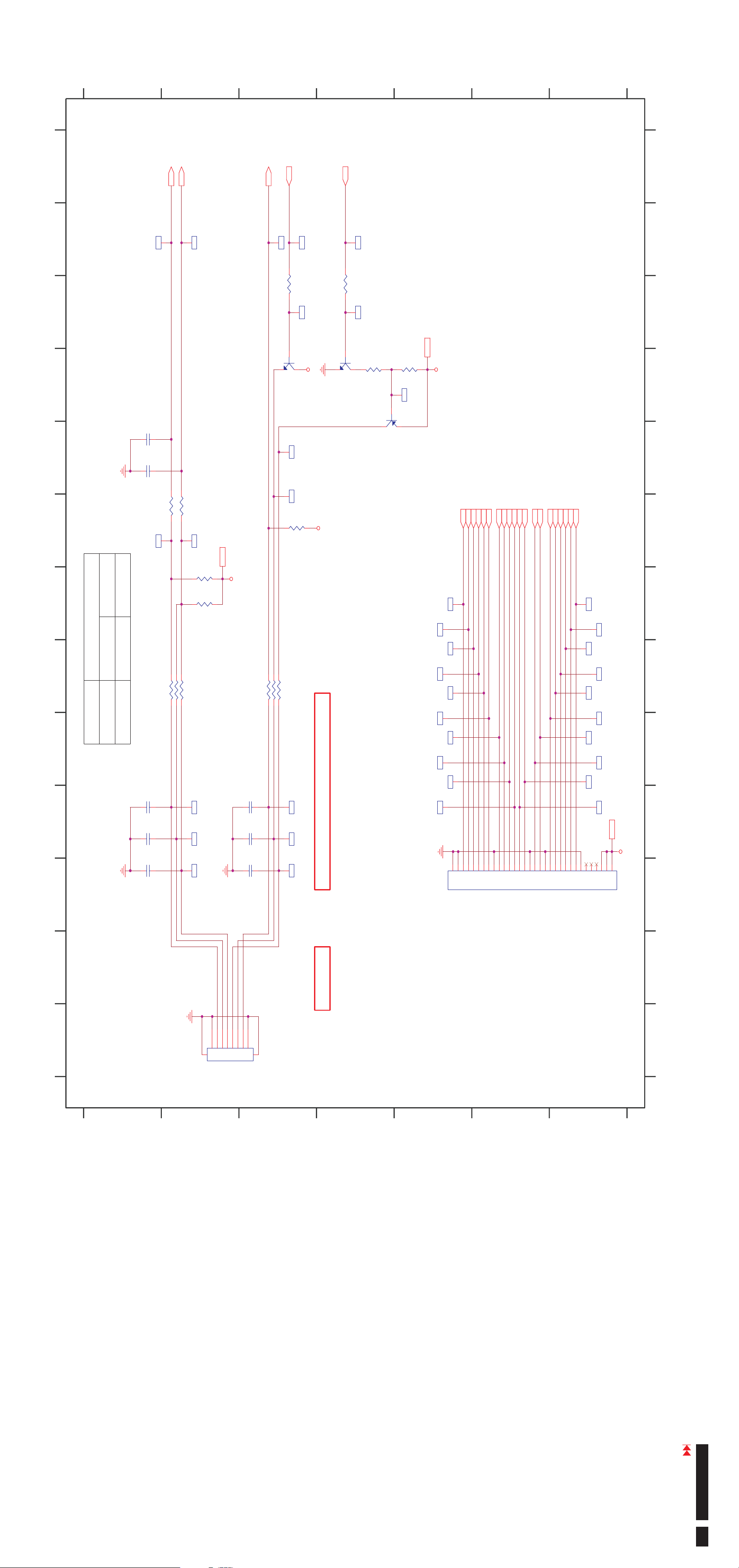
G
F
E
D
C
B
A
._86 _SCHEMATICS INTERFACE BD_KEY & PANEL INTERFACEHP_L1908W
1234567 8910111213
T147
LBADC IN1_
LBADC IN2_
PWR KEYn_
LED A_
LED B_
1234567 8910111213
LBADC IN1_
LBADC IN2_ LBADC IN2_
T141
LED A_
T140
T133
R374
2K4
T134
2
Q308
MMBT3904
VCC5V
3
1
LED B_
T131
R372
2K4
T132
2
1
3
Q307
MMBT3904
R371
10K
VCC5V
VCC5V
R370
10K
C387
0 1uF.
C388
0 1uF.
T148
MENU UP DOWN POWER/
2 46V 2 00V..
163V.
R383 100
R384 27K
T130
2
LBADC IN1_
T135
R380 100
3V3 DVDD1_
T142
3V3 DVDD1_
R378
10K
R379
10K
R382 15K
R381 27K
T136
3V3 DVDD1_
R373
10K
LED AMBER_
LED BLUE_
R375 200
R376 75 1/%
R377 1K
3
1
Q306
MMBT3906
CH2P LV E__
CH2N LV E__
CH2P LV E__
CH2N LV E__
CLKN LV E__
CLKP LV E__
CLKN LV E__
CLKP LV E__
CH3P LV E__
CH3N LV E__
CH3N LV E__
CH3P LV E__
T115
T110
T116
CH2N LV O__
CH2P LV O__
CH2N LV O__
CH2P LV O__
CLKN LV O__
CLKP LV O__
CLKN LV O__
CLKP LV O__
CH3N LV O__
CH3P LV O__
CH3N LV O__
CH3P LV O__
CH0N LV E__
CH0P LV E__
CH1P LV E__
CH1N LV E__
CH1P LV O__
CH0P LV O__
CH1N LV O__
CH0N LV O__
CH0P LV O__
CH0N LV O__
CH1P LV O__
CH1N LV O__
T120
T125
T121
CH1P LV E__
CH0P LV E__
CH0N LV E__
CH1N LV E__
T126
03V.
C390
0 1uF.
C391
0 1uF.
C392
0 1uF.
T144
T145
T146
KEY DOWNn_
KEY MENUn_
KEY UPn_
C384
0 1uF.
C385
0 1uF.
C386
0 1uF.
T137
T138
T139
BLUE LED_
AMBER LED_
KEY PWRn_PWR KEYn_
Del R385 C389 T143 P307,,, ,P308 Add P311
T122
T127
T123
T128
T124
T129
USE FFC WIRE FOR LVDS INTERFACE
CVILUX CF25302D0R0-
32
T111
T117
T112
T118
T113
T119
VLCD
T114
VLCD
P306
12345678910111213141516171819202122232425262728293031
PCB No.
6832176900P02
G
FFC 8Pin
F
KEY UPn_
KEY MENUn_
KEY DOWNn_
KEY PWRn_
AMBER LED_
BLUE LED_
P311
CON8
1234567
9
E
D
C
B
A
8
10
Go to cover page
HP L1908W
37
Page 39

G
F
E
D
C
B
A
.96 HP_L1908W_SCHEMATICS_AUDIO
1234567 8910111213
MMBT3904 NC()
1
VOLUME
Q310
VOLUME
T174
R395 2K4 NC()
T175
2
3
R393
2K4 NC()
VDD
VDD
3
AUDIO EN_
AUDIO EN_
R392 2K4 NC()
2
Q309
MMBT3906 NC()
1
T167
T168
R390
47K NC()
VDD
PBY160808T 301Y S NC--()
EGA10603V05A1 NC()
EGA10603V05A1 NC()
FB320
COLOR IS GREEN
T157
D324
C395
10nF NC()
D325
C396
10nF NC()
1
FB319
PBY160808T 301Y S NC--()
P309
PH JACK 3P Green NC--( )()
1234567 8910111213
3
2
T149
FB318
PBY160808T 301Y S NC--()
R396
120K NC()
C405
0 1uF NC.()
T172
R394 51K NC()
T173
100uF 16V NC/()
C401
0 1uF NC.()
PBY160808T 600Y S NC--()
AMP 5V_
C400
VDD
FB321
T169
T165
R391 100 NC()
T166
C398 0 47uF 0805 NC./()
T159
47K NC()
47K NC()
T160
C397 0 47uF 0805 NC./()
R388
R389
C394 0 47uF 0805 NC./()
R387 1K NC()
AUDIO IN R__
T156
C393 0 47uF 0805 NC./()
T150
T151
R386 1K NC()
AUDIO IN L__
T170
FB322 0 NC()
T171
0 47uF 0805 NC./()
0 47uF 0805 NC./()
0 47uF 0805 NC./()
C402
C403
C404
PVDD
TPA6021A4 NC()
PW GND_
3
9
PVDD
PW GND_
1611
VDD
AGND
17
0 47uF 0805 NC./()
NC
13
C399
AMP_PASS
16 15
BYPASS FADE
T164
03V 36V.~.
AMP VOLUME_
18
VOL
SE BEL/
19
T163
AMP STBYn_
14
SHUTDOWN
AMP IN R__+
4 2
RIN ROUT+-
AMP IN R__-
5
RIN-
ROUT+
20
OUT R_+
OUT R_-
T158
8
LIN+
LOUT-
10
OUT L_-
AMP IN L__+
LIN-
LOUT+
AMP IN L__-
7
12
OUT L_+
T152
T153
I310
PCB No. 6832176900P02
G
F
E
D
C
T161
T162
OUT R_+
JWT A2001WV2 04 NC--()
4
B
OUT R_-
2
3
OUT L_+
OUT L_-
1
T154
T155
P310
A
Go to cover page
HP L1908W
38
Page 40

1234567 8910111213
G
F
E
D
C
B
A
P600
910
5
6
7
8
1
2
3
4
1234567 8910111213
KEY POWERn_
LED AMBER_
LED GREEN_
KEY MENUn_
KEY DOWNn_
KEY UPn_
.6 10 HP_L1908W_SCHEMATICS_FUNCTION_KEY_BD
3 4
S604
1 2
KEY UPn_
UP KEY
3 4
S603
1 2
KEY DOWNn_
DOWN KEY
S602
MENU KEY
1 2
3 4
KEY MENUn_
3 4
S601
1 2
KEY POWERn_
POWER KEY
LED GREEN_
LED AMBER_
MENU POWER-+
Delete R608
LED GREEN_
C612
0 1uF.
C611
0 1uF.
1 3
LED
LED AMBER_
2 4
D601
LED AMBER_
LED GREEN_
PCB No.
6832192800P0B
G
F
E
D
C
B
A
Go to cover page
HP L1908W
39
Page 41

G
F
E
D
C
B
A
.6 11 HP_L1908W_LAYOUTS_POWER BOARD
1234567 8910111213
1234567 8910111213
PCB No.
G
F
E
D
C
B
A
Go to cover page
HP L1908W
40
Page 42

G
F
E
D
C
B
A
.6 12 HP_L1908W_LAYOUTS_INTERFACE BOARD
1234567 8910111213
1234567 8910111213
PCB No.
G
F
E
D
C
B
A
Go to cover page
HP L1908W
41
Page 43

G
F
E
D
C
B
A
.6 13 HP_L1908W_LAYOUTS_FUNCTION KEY BOARD AND USB BOARD
1234567 8910111213
1234567 8910111213
PCB No.
G
F
E
D
C
B
A
Go to cover page
HP L1908W
42
 Loading...